US6946995B2 - Microstrip patch antenna and array antenna using superstrate - Google Patents
Microstrip patch antenna and array antenna using superstrateDownload PDFInfo
- Publication number
- US6946995B2 US6946995B2US10/637,843US63784303AUS6946995B2US 6946995 B2US6946995 B2US 6946995B2US 63784303 AUS63784303 AUS 63784303AUS 6946995 B2US6946995 B2US 6946995B2
- Authority
- US
- United States
- Prior art keywords
- layer
- patch antenna
- dielectric
- patch
- microstrip
- Prior art date
- Legal status (The legal status is an assumption and is not a legal conclusion. Google has not performed a legal analysis and makes no representation as to the accuracy of the status listed.)
- Expired - Lifetime, expires
Links
Images


Classifications
- H—ELECTRICITY
- H01—ELECTRIC ELEMENTS
- H01Q—ANTENNAS, i.e. RADIO AERIALS
- H01Q21/00—Antenna arrays or systems
- H—ELECTRICITY
- H01—ELECTRIC ELEMENTS
- H01Q—ANTENNAS, i.e. RADIO AERIALS
- H01Q9/00—Electrically-short antennas having dimensions not more than twice the operating wavelength and consisting of conductive active radiating elements
- H01Q9/04—Resonant antennas
- H01Q9/0407—Substantially flat resonant element parallel to ground plane, e.g. patch antenna
- H01Q9/0414—Substantially flat resonant element parallel to ground plane, e.g. patch antenna in a stacked or folded configuration
- H—ELECTRICITY
- H01—ELECTRIC ELEMENTS
- H01Q—ANTENNAS, i.e. RADIO AERIALS
- H01Q1/00—Details of, or arrangements associated with, antennas
- H01Q1/40—Radiating elements coated with or embedded in protective material
- H—ELECTRICITY
- H01—ELECTRIC ELEMENTS
- H01Q—ANTENNAS, i.e. RADIO AERIALS
- H01Q19/00—Combinations of primary active antenna elements and units with secondary devices, e.g. with quasi-optical devices, for giving the antenna a desired directional characteristic
- H01Q19/06—Combinations of primary active antenna elements and units with secondary devices, e.g. with quasi-optical devices, for giving the antenna a desired directional characteristic using refracting or diffracting devices, e.g. lens
- H01Q19/062—Combinations of primary active antenna elements and units with secondary devices, e.g. with quasi-optical devices, for giving the antenna a desired directional characteristic using refracting or diffracting devices, e.g. lens for focusing
- H—ELECTRICITY
- H01—ELECTRIC ELEMENTS
- H01Q—ANTENNAS, i.e. RADIO AERIALS
- H01Q21/00—Antenna arrays or systems
- H01Q21/06—Arrays of individually energised antenna units similarly polarised and spaced apart
- H01Q21/061—Two dimensional planar arrays
- H01Q21/065—Patch antenna array
Definitions
- the present inventionrelates to a microstrip patch antenna and array antenna using a dielectric superstrate, and particularly to a microstrip patch antenna using a dielectric superstrate and an array antenna using the same, for a wireless communication base station, a wireless local area network, satellite communications and satellite broadcasting.
- microstrip radiatorswere first proposed by Deschamps as early as 1953. There are many advantages and disadvantages of microstrip antennas compared with other microwave antennas. The advantages include lightweight, low volume, low profile planar configurations and low fabrication cost. However, the microstrip antennas have disadvantages such as narrow bandwidth and low antenna gain.
- FIGS. 1A and 1Bare a cross-sectional view and a perspective view of a typical microstrip patch antenna.
- a typical microstrip patch antennahas a ground plane 101 , a dielectric layer 102 , a radiating patch 103 , and a feedline 104 .
- the dielectric layer 102is placed on the ground plane 101 that is a conductor and the feedline 104 and the radiating patch 103 are formed on the dielectric layer 102 .
- a structure of the typical microstrip patch antennadoes not provide broadband impedance characteristics.
- the number of radiating patchesare increased and the size of the antenna is enlarged.
- a microstrip patch antenna using a superstrateis disclosed by X. H. Shen in “Effect of superstrate on radiated field of probe fed microstrip patch antenna”, IEEE proc. Micro. Antenna Propag., Vol. 148, No. 3, pp. 131-146, 2001. 06.
- FIGS. 2A and 2Bare a cross-sectional view and a perspective view of a microstrip patch antenna using superstrate disclosed by X. H. Shen.
- a microstrip patchis fed by a coaxial cable.
- a dielectric layer having high permittivityis formed on the microstrip patch, radiating field is focused on boresight direction.
- the microstrip antenna of FIGS. 2A and 2Bhas a problem such as a narrow impedance bandwidth because a radiating patch is on a single layer substrate and it is not adequate to make an array antenna by using the microstrip antenna of FIGS. 2A because the radiating patch is fed to the coaxial cable.
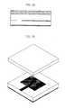
- FIGS. 3A and 3Bare a cross-sectional view and a perspective view of a conventional microstrip stacked patch antenna printed on dielectric film which is disclosed at Korean Patent application No. 2001-47913.
- a dielectric layer 102is placed on a ground plane 101 , and a feedline 104 and a first radiating patch 103 are formed on the dielectric layer 102 .
- a foam layer 301is placed on the feedline 104 and the lower radiating patch 103 , a dielectric film 302 is formed on the foam layer 301 , and a upper radiating patch 303 is placed on the dielectric film 302 .
- the stacked layers of the microstrip patch antennais proper to enhance impedance bandwidth characteristics, the antenna gain is not high enough to meet the requirement of the current needs such as a wireless communication base station, a wireless local area network, satellite communications and satellite broadcasting.
- a microstrip patch antenna using a dielectric superstrate for having high gain and broadbandincluding: a lower patch antenna layer having a dielectric layer and a ground plane, for radiating energy by exciting current by a feedline electrically connected to a lower radiating patch on a side of the dielectric layer; an upper patches on a dielectric film electromagnetically coupled by the lower radiating patch; a foam layer for distancing the upper patch antenna layer from the lower patch antenna layer by arranging the foam layer between the lower patch antenna layer and the upper patch antenna layer; and a dielectric superstrate located with predeteremined distance from the upper patch antenna layer.
- a microstrip array antennaincluding microstrip patch antennas, each of which uses a dielectric superstrate
- the microstrip patch antennaincludes: a lower patch antenna layer having a dielectric layer and a ground plane, for radiating energy by exciting current by a feedline electrically connected to a lower radiating patch on a side of the dielectric layer; an upper patches on a dielectric film electromagnetically coupled by the lower radiating patch; a foam layer for distancing the upper patch antenna layer from the lower patch antenna layer by arranging the foam layer between the lower patch antenna layer and the upper patch antenna layer; and a dielectric superstrate located with predeteremined distance from the upper patch antenna layer,
- the array antennais designed using the corporate feeding method and the element spacing of the microstrip patch antennas is more than 1 ⁇ 0 at 12 GHz to minimize the coupling, wherein although the element spacing in the array is wider than the wavelength in free space, the grating lobes can be reduced by the superstrate.
- FIGS. 1A and 1Bare a cross-sectional view and a perspective view of a typical microstrip patch antenna
- FIGS. 2A and 2Bare a cross-sectional view and a perspective view of a conventional microstrip patch antenna using superstrate;
- FIGS. 3A and 3Bare a cross-sectional view and a perspective view of a conventional microstrip stacked patch antenna printed on a dielectric film;
- FIGS. 4A and 4Bare a cross-sectional view and a perspective view of a microstrip patch antenna in accordance with the present invention.
- FIG. 5Ais a cross-sectional view of a microstrip array antenna using a dielectric superstrate in accordance with the present invention and is an array structure of the microstrip patch antenna of FIG. 4A ;
- FIGS. 5B and 5Care top views of a dielectric layer and a dielectric film in accordance with the present invention.
- FIG. 6is a graph showing gain characteristics and return loss bandwidth characteristics of a microstrip patch antenna having a superstrate shown in FIG. 4 and a microstrip patch antenna without a superstrate shown in FIG. 3 ;
- FIGS. 7 , 8 A and 8 Bare graphs showing measured return loss and radiation pattern of a microstrip patch antenna using dielectric superstrate in accordance with the present invention.
- FIGS. 4A and 4Bare a cross-sectional view and a perspective view of a microstrip patch antenna in accordance with the present invention.
- a dielectric layer 102is formed on a ground plane 101 , and a feedline 104 and a lower radiating patch 103 are formed on the dielectric layer 102 in the microstrip patch antenna in accordance with the present invention.
- the feedline 104is electrically connected to the lower radiating patch 103 .
- a foam layer 301is formed on the feedline 104 and the lower radiating patch 103 , a dielectric film 302 is formed on the foam layer 301 , and an upper radiating patch 303 is placed on the dielectric film 302 .
- An airgap 401 having a predetermined thicknessis placed on the upper radiating patch 303 and a high permittivity dielectric superstrate 402 having a predetermined thickness is formed over the airgap 401 .
- the upper radiating patchis stacked upon the lower radiating patch ( 103 ) by electromagnetically coupling each other efficiently.
- Coupling efficiencyis obtained by electromagnetically coupling the upper radiating patch 303 to the lower radiating patch 103 that is connected to the feedline 104 .
- the bandwidth and the gain of the antennaare determined by the thickness of the dielectric superstrate 402 and a dielectric constant. Also, resonant characteristics can be largely varied by the thickness of the airgap 410 .
- the gainis increased but the bandwidth becomes narrow. If the thin dielectric superstrate 402 and low dielectric constant are used, the gain tends to be decreased but the impedance bandwidth tends to be broadened.
- FIG. 5Ais cross-sectional view of a microstrip array antenna using dielectric superstrate in accordance with the present invention.
- the microstrip array antenna of FIG. 5Ais array structure of single radiating element.
- FIGS. 5B and 5Care top views of a dielectric layer and a dielectric film in accordance with the present invention.
- the microstrip patch antennais designed so that radiation field radiated from each radiating patch can obtain a high directivity in the dielectric layer 402 .
- the distance between each radiating patchesis more than 1 ⁇ 0 in this embodiment.
- the thickness of the dielectric layer 402 and the dielectric constantcan largely affect the bandwidth and the gain characteristics.
- FIG. 6is a graph showing gain characteristics and return loss bandwidth characteristics of a microstrip patch antenna with a superstrate shown in FIG. 4 and a microstrip patch antenna without a superstrate shown in FIG. 3 .
- FIGS. 7 , 8 A and 8 Bare graphs showing measured return loss and radiation pattern of a microstrip patch antenna using dielectric superstrate in accordance with the present invention.
- the microstrip patch antenna using dielectric superstrate in accordance with the present inventionoutperforms the conventional microstrip patch antenna.
- the gain of the microstrip patch antenna using dielectric superstrate in accordance with the present inventionis enhanced about 4 dBi than that of the conventional microstrip patch antenna.
- 10 dB return loss bandwidthis 12.6%, i.e., center frequency is 12 GHz, side lobe level in E-plane is less than 10 dB, side lobe level in H-plane is less than 15 dB, and cross polarization level is less than 25 at boresight.
- 2 ⁇ 8 microstrip array antenna in accordance with the present inventionhas the gain of about 23 dBi which is about 3 dBi higher than the prior microstrip array antenna.
- the present inventioncan improve performances of antenna gain, radiation efficiency, and bandwidth characteristics by using radiation element having wide impedance bandwidth and dielectric layer having high permittivity.
- a size of the microstrip antenna used in satellite communication systems and satellite broadcasting systemsis reduced by using the present invention.
- the present inventioncan also be used in the field of wireless local area network because of the high gain characteristics of the present invention.
Landscapes
- Waveguide Aerials (AREA)
- Variable-Direction Aerials And Aerial Arrays (AREA)
Abstract
Description
Claims (6)
Applications Claiming Priority (2)
| Application Number | Priority Date | Filing Date | Title |
|---|---|---|---|
| KR2002-75401 | 2002-11-29 | ||
| KR10-2002-0075401AKR100485354B1 (en) | 2002-11-29 | 2002-11-29 | Microstrip Patch Antenna and Array Antenna Using Superstrate |
Publications (2)
| Publication Number | Publication Date |
|---|---|
| US20040104852A1 US20040104852A1 (en) | 2004-06-03 |
| US6946995B2true US6946995B2 (en) | 2005-09-20 |
Family
ID=32388280
Family Applications (1)
| Application Number | Title | Priority Date | Filing Date |
|---|---|---|---|
| US10/637,843Expired - LifetimeUS6946995B2 (en) | 2002-11-29 | 2003-08-08 | Microstrip patch antenna and array antenna using superstrate |
Country Status (2)
| Country | Link |
|---|---|
| US (1) | US6946995B2 (en) |
| KR (1) | KR100485354B1 (en) |
Cited By (22)
| Publication number | Priority date | Publication date | Assignee | Title |
|---|---|---|---|---|
| US20050275590A1 (en)* | 2004-06-10 | 2005-12-15 | Soon-Young Eom | Microstrip stack patch antenna using multilayered metallic disk array and planar array antenna using the same |
| US20070096852A1 (en)* | 2005-06-25 | 2007-05-03 | Qinetiq Limited | Electromagnetic radiation decoupler |
| US20070229363A1 (en)* | 2006-03-29 | 2007-10-04 | Fujitsu Component Limited | Antenna device |
| US20070290941A1 (en)* | 2006-06-16 | 2007-12-20 | Qinetiq Limited | Electromagnetic Enhancement and Decoupling |
| US20090251362A1 (en)* | 2008-04-04 | 2009-10-08 | Alexandros Margomenos | Three dimensional integrated automotive radars and methods of manufacturing the same |
| US20090251357A1 (en)* | 2008-04-04 | 2009-10-08 | Toyota Motor Engineering & Manufacturing North America, Inc. | Dual-band antenna array and rf front-end for mm-wave imager and radar |
| US20100007561A1 (en)* | 2008-05-23 | 2010-01-14 | Steven Bucca | Broadband patch antenna and antenna system |
| US20100045025A1 (en)* | 2008-08-20 | 2010-02-25 | Omni-Id Limited | One and Two-Part Printable EM Tags |
| US20100073236A1 (en)* | 2008-09-23 | 2010-03-25 | Frank Mierke | Multilayer antenna arrangement |
| US20100182107A1 (en)* | 2009-01-16 | 2010-07-22 | Toyota Motor Engineering & Manufacturing North America,Inc. | System and method for improving performance of coplanar waveguide bends at mm-wave frequencies |
| US20100230497A1 (en)* | 2006-12-20 | 2010-09-16 | Omni-Id Limited | Radiation Enhancement and Decoupling |
| US7830301B2 (en) | 2008-04-04 | 2010-11-09 | Toyota Motor Engineering & Manufacturing North America, Inc. | Dual-band antenna array and RF front-end for automotive radars |
| US20110037541A1 (en)* | 2006-12-14 | 2011-02-17 | Omni-Id Limited | Switchable Radiation Enhancement and Decoupling |
| CN103531891A (en)* | 2013-10-24 | 2014-01-22 | 哈尔滨工程大学 | Wideband High Gain Probe and Patch Tangent Stacked Microstrip Antenna |
| US8736502B1 (en) | 2008-08-08 | 2014-05-27 | Ball Aerospace & Technologies Corp. | Conformal wide band surface wave radiating element |
| US8786496B2 (en) | 2010-07-28 | 2014-07-22 | Toyota Motor Engineering & Manufacturing North America, Inc. | Three-dimensional array antenna on a substrate with enhanced backlobe suppression for mm-wave automotive applications |
| US9590292B2 (en) | 2014-12-08 | 2017-03-07 | Industrial Technology Research Institute | Beam antenna |
| US9722315B2 (en) | 2013-02-11 | 2017-08-01 | Samsung Electronics Co., Ltd. | Ultra-wideband (UWB) dipole antenna |
| US10135133B2 (en) | 2016-05-26 | 2018-11-20 | The Chinese University Of Hong Kong | Apparatus and methods for reducing mutual couplings in an antenna array |
| US11088458B2 (en) | 2017-12-31 | 2021-08-10 | Amir Jafargholi | Reducing mutual coupling and back-lobe radiation of a microstrip antenna |
| US11374327B2 (en)* | 2020-03-30 | 2022-06-28 | The Boeing Company | Microstrip to microstrip vialess transition |
| DE202022103232U1 (en) | 2022-06-08 | 2022-11-05 | Raghvendra Sarvjeet Dubey | A system for synthesizing dielectric ceramic nanoparticles for microstrip patch antennas |
Families Citing this family (42)
| Publication number | Priority date | Publication date | Assignee | Title |
|---|---|---|---|---|
| US6947008B2 (en)* | 2003-01-31 | 2005-09-20 | Ems Technologies, Inc. | Conformable layered antenna array |
| KR100611806B1 (en)* | 2004-03-03 | 2006-08-10 | 주식회사 케이엠더블유 | Dual polarization base station antenna with stacked patch radiating element for probe feeding and its control system |
| CN101065881B (en)* | 2004-05-21 | 2012-05-16 | 艾利森电话股份有限公司 | Broadband array antennas using complementary antenna |
| WO2006091131A1 (en)* | 2005-02-25 | 2006-08-31 | Telefonaktiebolaget Lm Ericsson (Publ) | Uniform communication unit |
| JP4500214B2 (en)* | 2005-05-30 | 2010-07-14 | 株式会社日立製作所 | Wireless IC tag and method of manufacturing wireless IC tag |
| EP1772748A1 (en)* | 2005-10-05 | 2007-04-11 | Sony Deutschland GmbH | Microwave alignment apparatus |
| KR100896537B1 (en) | 2007-11-15 | 2009-05-07 | 주식회사 아모텍 | Built-in antenna with air gap |
| KR100870996B1 (en)* | 2007-02-22 | 2008-11-27 | 주식회사 아모텍 | Built-in antenna |
| US20100097272A1 (en)* | 2007-02-22 | 2010-04-22 | Amotech Co., Ltd. | Internal antenna with air gap |
| KR100971469B1 (en)* | 2010-03-10 | 2010-07-22 | (주)건축사사무소 성우건축 | Electric terminal box |
| TWI481116B (en)* | 2011-08-25 | 2015-04-11 | Ind Tech Res Inst | Antenna structure |
| US10126180B2 (en) | 2013-09-27 | 2018-11-13 | Brain Temp Inc. | Apparatuses for non-invasively sensing internal temperature |
| KR102185196B1 (en)* | 2014-07-04 | 2020-12-01 | 삼성전자주식회사 | Apparatus for antenna in wireless communication device |
| US9716320B2 (en)* | 2014-10-10 | 2017-07-25 | Cambium Networks Limited | Patch antenna-based wideband antenna system |
| US9548541B2 (en)* | 2015-03-30 | 2017-01-17 | Huawei Technologies Canada Co., Ltd. | Apparatus and method for a high aperture efficiency broadband antenna element with stable gain |
| KR102158031B1 (en)* | 2016-07-11 | 2020-09-21 | (주)탑중앙연구소 | Microstrip stacked patch antenna |
| US10971806B2 (en) | 2017-08-22 | 2021-04-06 | The Boeing Company | Broadband conformal antenna |
| KR101954000B1 (en)* | 2017-11-22 | 2019-03-04 | 홍익대학교 산학협력단 | Antenna using pin feeding and top laminated structure |
| US10826180B2 (en) | 2017-11-29 | 2020-11-03 | The Board Of Trustees Of The University Of Alabama | Low-profile multi-band stacked patch antenna |
| CN109935964B (en)* | 2017-12-15 | 2021-04-09 | 华为技术有限公司 | An antenna unit and antenna array |
| US11233310B2 (en)* | 2018-01-29 | 2022-01-25 | The Boeing Company | Low-profile conformal antenna |
| KR102377589B1 (en)* | 2018-04-02 | 2022-03-24 | 한국전자통신연구원 | Linear slot array antenna for broadly scanning frequency |
| CN109066071A (en)* | 2018-04-26 | 2018-12-21 | 西安电子科技大学 | A kind of Compact type broadband flexibility microstrip antenna |
| US10916853B2 (en) | 2018-08-24 | 2021-02-09 | The Boeing Company | Conformal antenna with enhanced circular polarization |
| US10923831B2 (en) | 2018-08-24 | 2021-02-16 | The Boeing Company | Waveguide-fed planar antenna array with enhanced circular polarization |
| US10938082B2 (en) | 2018-08-24 | 2021-03-02 | The Boeing Company | Aperture-coupled microstrip-to-waveguide transitions |
| KR102548573B1 (en)* | 2018-11-06 | 2023-06-28 | 삼성전자 주식회사 | Antenna and electronic device including dielectric material overlapped with at least a portion of the antenna |
| CN109411900B (en)* | 2018-12-14 | 2024-08-09 | 华诺星空技术股份有限公司 | Broadband antenna for through-wall radar imaging |
| CN110021812B (en) | 2019-04-08 | 2021-04-13 | Oppo广东移动通信有限公司 | Antenna components and electronic equipment |
| US11276933B2 (en) | 2019-11-06 | 2022-03-15 | The Boeing Company | High-gain antenna with cavity between feed line and ground plane |
| KR102254880B1 (en)* | 2019-12-06 | 2021-05-24 | 삼성전기주식회사 | Chip antenna module array and chip antenna module |
| KR102423963B1 (en) | 2020-03-31 | 2022-07-21 | 동우 화인켐 주식회사 | Antenna stack structure and display device |
| CN111753434B (en)* | 2020-07-03 | 2022-06-07 | 湖南华诺星空电子技术有限公司 | Ultra-narrow-band navigation interference antenna design method, antenna and application thereof |
| CN112018512A (en)* | 2020-08-14 | 2020-12-01 | 中北大学 | A small planar medical directional microwave resonant antenna |
| KR102267314B1 (en)* | 2020-09-17 | 2021-06-21 | 한화시스템 주식회사 | Resonant cavity antenna |
| KR102532615B1 (en)* | 2020-10-30 | 2023-05-16 | 재단법인 파동에너지 극한제어 연구단 | Dual-band electromagnetic wave absorber with metasurface |
| KR102532609B1 (en)* | 2020-10-30 | 2023-05-16 | 재단법인 파동에너지 극한제어 연구단 | Electromagnetic wave absorber with metasurface |
| CN113224525B (en)* | 2021-05-31 | 2024-07-09 | 浙江嘉科电子有限公司 | High-gain double-frequency omnidirectional antenna for 5G communication |
| KR102427628B1 (en)* | 2021-11-11 | 2022-08-02 | 한화시스템 주식회사 | Rading element, antenna apparatus and manufacturing for antenna apparatus |
| CN114883792B (en)* | 2021-12-17 | 2023-07-28 | 长沙理工大学 | Low-frequency high-gain narrow-band antenna connected with ipex joint |
| CN114858823B (en)* | 2022-04-19 | 2025-04-22 | 武汉理工大学 | A microstrip antenna sensor |
| CN115548663A (en)* | 2022-09-30 | 2022-12-30 | 维沃移动通信有限公司 | wearable device |
Citations (5)
| Publication number | Priority date | Publication date | Assignee | Title |
|---|---|---|---|---|
| JPH1184409A (en) | 1997-09-01 | 1999-03-26 | Canon Inc | Still image display device |
| US6075485A (en)* | 1998-11-03 | 2000-06-13 | Atlantic Aerospace Electronics Corp. | Reduced weight artificial dielectric antennas and method for providing the same |
| US6359588B1 (en)* | 1997-07-11 | 2002-03-19 | Nortel Networks Limited | Patch antenna |
| US6650294B2 (en)* | 2001-11-26 | 2003-11-18 | Telefonaktiebolaget Lm Ericsson (Publ) | Compact broadband antenna |
| US20040104847A1 (en)* | 2002-12-03 | 2004-06-03 | Killen William D. | High efficiency slot fed microstrip patch antenna |
Family Cites Families (6)
| Publication number | Priority date | Publication date | Assignee | Title |
|---|---|---|---|---|
| US5187490A (en)* | 1989-08-25 | 1993-02-16 | Hitachi Chemical Company, Ltd. | Stripline patch antenna with slot plate |
| CA2061254C (en)* | 1991-03-06 | 2001-07-03 | Jean Francois Zurcher | Planar antennas |
| KR19990084409A (en)* | 1998-05-06 | 1999-12-06 | 윤종용 | Planar Antenna Using Multi-layer Dielectric with Honeycomb Layer |
| KR19990084408A (en)* | 1998-05-06 | 1999-12-06 | 윤종용 | Planar antenna using multilayer dielectric with air layer |
| KR100702774B1 (en)* | 2000-03-22 | 2007-04-03 | 주식회사 케이티 | Dual feeding dual resonance antenna structure |
| KR100449846B1 (en)* | 2001-12-26 | 2004-09-22 | 한국전자통신연구원 | Circular Polarized Microstrip Patch Antenna and Array Antenna arraying it for Sequential Rotation Feeding |
- 2002
- 2002-11-29KRKR10-2002-0075401Apatent/KR100485354B1/ennot_activeExpired - Fee Related
- 2003
- 2003-08-08USUS10/637,843patent/US6946995B2/ennot_activeExpired - Lifetime
Patent Citations (5)
| Publication number | Priority date | Publication date | Assignee | Title |
|---|---|---|---|---|
| US6359588B1 (en)* | 1997-07-11 | 2002-03-19 | Nortel Networks Limited | Patch antenna |
| JPH1184409A (en) | 1997-09-01 | 1999-03-26 | Canon Inc | Still image display device |
| US6075485A (en)* | 1998-11-03 | 2000-06-13 | Atlantic Aerospace Electronics Corp. | Reduced weight artificial dielectric antennas and method for providing the same |
| US6650294B2 (en)* | 2001-11-26 | 2003-11-18 | Telefonaktiebolaget Lm Ericsson (Publ) | Compact broadband antenna |
| US20040104847A1 (en)* | 2002-12-03 | 2004-06-03 | Killen William D. | High efficiency slot fed microstrip patch antenna |
Non-Patent Citations (1)
| Title |
|---|
| "A Novel Low Profile Slot-multi-layer Patch Antenna", M. Fan, et al., 2001 IEEE, pp. 196-201. |
Cited By (45)
| Publication number | Priority date | Publication date | Assignee | Title |
|---|---|---|---|---|
| US7307587B2 (en)* | 2004-06-10 | 2007-12-11 | Electronics And Telecommunications Research Institute | High-gain radiating element structure using multilayered metallic disk array |
| US20050275590A1 (en)* | 2004-06-10 | 2005-12-15 | Soon-Young Eom | Microstrip stack patch antenna using multilayered metallic disk array and planar array antenna using the same |
| US8299927B2 (en) | 2005-06-25 | 2012-10-30 | Omni-Id Cayman Limited | Electromagnetic radiation decoupler |
| US9646241B2 (en) | 2005-06-25 | 2017-05-09 | Omni-Id Cayman Limited | Electromagnetic radiation decoupler |
| US9104952B2 (en) | 2005-06-25 | 2015-08-11 | Omni-Id Cayman Limited | Electromagnetic radiation decoupler |
| US20070096852A1 (en)* | 2005-06-25 | 2007-05-03 | Qinetiq Limited | Electromagnetic radiation decoupler |
| US20110121079A1 (en)* | 2005-06-25 | 2011-05-26 | Omni-Id Limited | Electromagnetic Radiation Decoupler |
| US7768400B2 (en) | 2005-06-25 | 2010-08-03 | Omni-Id Limited | Electromagnetic radiation decoupler |
| US20070229363A1 (en)* | 2006-03-29 | 2007-10-04 | Fujitsu Component Limited | Antenna device |
| US7382331B2 (en)* | 2006-03-29 | 2008-06-03 | Fujitsu Component Limited | Antenna device |
| US20070290941A1 (en)* | 2006-06-16 | 2007-12-20 | Qinetiq Limited | Electromagnetic Enhancement and Decoupling |
| US7880619B2 (en) | 2006-06-16 | 2011-02-01 | Omni-Id Limited | Electromagnetic enhancement and decoupling |
| US8264358B2 (en) | 2006-06-16 | 2012-09-11 | Omni-Id Cayman Limited | Electromagnetic enhancement and decoupling |
| US8502678B2 (en) | 2006-06-16 | 2013-08-06 | Omni-Id Cayman Limited | Electromagnetic enhancement and decoupling |
| US8453936B2 (en) | 2006-12-14 | 2013-06-04 | Omni-Id Cayman Limited | Switchable radiation enhancement and decoupling |
| US20110037541A1 (en)* | 2006-12-14 | 2011-02-17 | Omni-Id Limited | Switchable Radiation Enhancement and Decoupling |
| US20100230497A1 (en)* | 2006-12-20 | 2010-09-16 | Omni-Id Limited | Radiation Enhancement and Decoupling |
| US8684270B2 (en) | 2006-12-20 | 2014-04-01 | Omni-Id Cayman Limited | Radiation enhancement and decoupling |
| US7830301B2 (en) | 2008-04-04 | 2010-11-09 | Toyota Motor Engineering & Manufacturing North America, Inc. | Dual-band antenna array and RF front-end for automotive radars |
| US8305255B2 (en)* | 2008-04-04 | 2012-11-06 | Toyota Motor Engineering & Manufacturing North America, Inc. | Dual-band antenna array and RF front-end for MM-wave imager and radar |
| US7733265B2 (en) | 2008-04-04 | 2010-06-08 | Toyota Motor Engineering & Manufacturing North America, Inc. | Three dimensional integrated automotive radars and methods of manufacturing the same |
| US8305259B2 (en) | 2008-04-04 | 2012-11-06 | Toyota Motor Engineering & Manufacturing North America, Inc. | Dual-band antenna array and RF front-end for mm-wave imager and radar |
| US8022861B2 (en) | 2008-04-04 | 2011-09-20 | Toyota Motor Engineering & Manufacturing North America, Inc. | Dual-band antenna array and RF front-end for mm-wave imager and radar |
| US20090251357A1 (en)* | 2008-04-04 | 2009-10-08 | Toyota Motor Engineering & Manufacturing North America, Inc. | Dual-band antenna array and rf front-end for mm-wave imager and radar |
| US20090251362A1 (en)* | 2008-04-04 | 2009-10-08 | Alexandros Margomenos | Three dimensional integrated automotive radars and methods of manufacturing the same |
| US8232924B2 (en) | 2008-05-23 | 2012-07-31 | Alliant Techsystems Inc. | Broadband patch antenna and antenna system |
| US20100007561A1 (en)* | 2008-05-23 | 2010-01-14 | Steven Bucca | Broadband patch antenna and antenna system |
| US8736502B1 (en) | 2008-08-08 | 2014-05-27 | Ball Aerospace & Technologies Corp. | Conformal wide band surface wave radiating element |
| US8636223B2 (en) | 2008-08-20 | 2014-01-28 | Omni-Id Cayman Limited | One and two-part printable EM tags |
| US8794533B2 (en) | 2008-08-20 | 2014-08-05 | Omni-Id Cayman Limited | One and two-part printable EM tags |
| US20100045025A1 (en)* | 2008-08-20 | 2010-02-25 | Omni-Id Limited | One and Two-Part Printable EM Tags |
| US20100073236A1 (en)* | 2008-09-23 | 2010-03-25 | Frank Mierke | Multilayer antenna arrangement |
| US7936306B2 (en)* | 2008-09-23 | 2011-05-03 | Kathrein-Werke Kg | Multilayer antenna arrangement |
| US7990237B2 (en) | 2009-01-16 | 2011-08-02 | Toyota Motor Engineering & Manufacturing North America, Inc. | System and method for improving performance of coplanar waveguide bends at mm-wave frequencies |
| US20100182107A1 (en)* | 2009-01-16 | 2010-07-22 | Toyota Motor Engineering & Manufacturing North America,Inc. | System and method for improving performance of coplanar waveguide bends at mm-wave frequencies |
| US8786496B2 (en) | 2010-07-28 | 2014-07-22 | Toyota Motor Engineering & Manufacturing North America, Inc. | Three-dimensional array antenna on a substrate with enhanced backlobe suppression for mm-wave automotive applications |
| US9722315B2 (en) | 2013-02-11 | 2017-08-01 | Samsung Electronics Co., Ltd. | Ultra-wideband (UWB) dipole antenna |
| CN103531891B (en)* | 2013-10-24 | 2015-07-22 | 哈尔滨工程大学 | Broadband high-gain probe and patch tangent stacked microstrip antenna |
| CN103531891A (en)* | 2013-10-24 | 2014-01-22 | 哈尔滨工程大学 | Wideband High Gain Probe and Patch Tangent Stacked Microstrip Antenna |
| US9590292B2 (en) | 2014-12-08 | 2017-03-07 | Industrial Technology Research Institute | Beam antenna |
| US10135133B2 (en) | 2016-05-26 | 2018-11-20 | The Chinese University Of Hong Kong | Apparatus and methods for reducing mutual couplings in an antenna array |
| JP2019519988A (en)* | 2016-05-26 | 2019-07-11 | ザ チャイニーズ ユニバーシティー オブ ホンコンThe Chinese University Of Hongkong | Apparatus and method for reducing mutual coupling in an antenna array |
| US11088458B2 (en) | 2017-12-31 | 2021-08-10 | Amir Jafargholi | Reducing mutual coupling and back-lobe radiation of a microstrip antenna |
| US11374327B2 (en)* | 2020-03-30 | 2022-06-28 | The Boeing Company | Microstrip to microstrip vialess transition |
| DE202022103232U1 (en) | 2022-06-08 | 2022-11-05 | Raghvendra Sarvjeet Dubey | A system for synthesizing dielectric ceramic nanoparticles for microstrip patch antennas |
Also Published As
| Publication number | Publication date |
|---|---|
| KR100485354B1 (en) | 2005-04-28 |
| KR20040047257A (en) | 2004-06-05 |
| US20040104852A1 (en) | 2004-06-03 |
Similar Documents
| Publication | Publication Date | Title |
|---|---|---|
| US6946995B2 (en) | Microstrip patch antenna and array antenna using superstrate | |
| US7099686B2 (en) | Microstrip patch antenna having high gain and wideband | |
| US9929472B2 (en) | Phased array antenna | |
| US7986279B2 (en) | Ring-slot radiator for broad-band operation | |
| US7423593B2 (en) | Broadside high-directivity microstrip patch antennas | |
| US20220407231A1 (en) | Wideband electromagnetically coupled microstrip patch antenna for 60 ghz millimeter wave phased array | |
| US10978812B2 (en) | Single layer shared aperture dual band antenna | |
| Cono | A low-cost suspended patch antenna for WLAN access points and point-to-point links | |
| US7598918B2 (en) | Tubular endfire slot-mode antenna array with inter-element coupling and associated methods | |
| US20070132643A1 (en) | Dual polarization antenna array with inter-element coupling and associated methods | |
| CA2617850A1 (en) | Dual-polarization, slot-mode antenna and associated methods | |
| KR100683005B1 (en) | Microstrip Stack Patch Antenna Using Multi-layer Circular Conductor Array and Planar Array Antenna Using Them | |
| EP1798817A1 (en) | Single polarization slot antenna array with inter-element capacitive coupling plate and associated methods | |
| Zhao et al. | Low-profile broadband dual-polarized integrated patch subarray for X-band synthetic aperture radar payload on small satellite | |
| Parthasarathy et al. | Design of linear 2× 2 array using substrate-integrated-waveguide patch antenna for 28GHz mm-wave applications | |
| Dalvi et al. | High gain wideband 2× 2 microstrip array antenna using RIS and Fabry Perot Cavity resonator | |
| US7408519B2 (en) | Dual polarization antenna array with inter-element capacitive coupling plate and associated methods | |
| Eldek et al. | A microstrip-fed modified printed bow-tie antenna for simultaneous operation in the C and X-bands | |
| Lee et al. | Broadband high‐efficiency microstrip antenna array with corporate‐series‐feed | |
| Khan et al. | A Fabry-Perot cavity antenna with a SiGe on-chip feeder for submm-wave applications | |
| Yun et al. | Design and analysis of TX/RX dual microstrip antenna using FDTD at Ku-band | |
| Lin et al. | Ultra-Thin Uniform Linear Array of Electrically Small Huygens Dipole Antennas | |
| Isa et al. | Analysis of Aperture Coupled Circular Patch Antenna for Mid-Band 5G | |
| Soliman et al. | Novel microstrip antenna element and 2‐by‐2 array for satellite TV receivers | |
| Rubelj et al. | A microstrip antenna array for direct broadcast satellite receivers |
Legal Events
| Date | Code | Title | Description |
|---|---|---|---|
| AS | Assignment | Owner name:ELECTRONICS AND TELECOMMUNICATIONS RESEARCH INSTIT Free format text:ASSIGNMENT OF ASSIGNORS INTEREST;ASSIGNORS:CHOI, WON KYU;PYO, CHEOLL SIG;LEE, JONG MOON;AND OTHERS;REEL/FRAME:014388/0736;SIGNING DATES FROM 20030616 TO 20030701 | |
| STCF | Information on status: patent grant | Free format text:PATENTED CASE | |
| FEPP | Fee payment procedure | Free format text:PAYOR NUMBER ASSIGNED (ORIGINAL EVENT CODE: ASPN); ENTITY STATUS OF PATENT OWNER: LARGE ENTITY | |
| FEPP | Fee payment procedure | Free format text:PAYOR NUMBER ASSIGNED (ORIGINAL EVENT CODE: ASPN); ENTITY STATUS OF PATENT OWNER: LARGE ENTITY Free format text:PAYER NUMBER DE-ASSIGNED (ORIGINAL EVENT CODE: RMPN); ENTITY STATUS OF PATENT OWNER: LARGE ENTITY | |
| FPAY | Fee payment | Year of fee payment:4 | |
| AS | Assignment | Owner name:IPG ELECTRONICS 502 LIMITED Free format text:ASSIGNMENT OF ONE HALF (1/2) OF ALL OF ASSIGNORS' RIGHT, TITLE AND INTEREST;ASSIGNOR:ELECTRONICS AND TELECOMMUNICATIONS RESEARCH INSTITUTE;REEL/FRAME:023456/0363 Effective date:20081226 | |
| FEPP | Fee payment procedure | Free format text:PAYOR NUMBER ASSIGNED (ORIGINAL EVENT CODE: ASPN); ENTITY STATUS OF PATENT OWNER: LARGE ENTITY Free format text:PAYER NUMBER DE-ASSIGNED (ORIGINAL EVENT CODE: RMPN); ENTITY STATUS OF PATENT OWNER: LARGE ENTITY | |
| FEPP | Fee payment procedure | Free format text:PAT HOLDER NO LONGER CLAIMS SMALL ENTITY STATUS, ENTITY STATUS SET TO UNDISCOUNTED (ORIGINAL EVENT CODE: STOL); ENTITY STATUS OF PATENT OWNER: LARGE ENTITY | |
| AS | Assignment | Owner name:PENDRAGON ELECTRONICS AND TELECOMMUNICATIONS RESEA Free format text:ASSIGNMENT OF ASSIGNORS INTEREST;ASSIGNORS:IPG ELECTRONICS 502 LIMITED;ELECTRONICS AND TELECOMMUNICATIONS RESEARCH INSTITUTE;SIGNING DATES FROM 20120410 TO 20120515;REEL/FRAME:028611/0643 | |
| FPAY | Fee payment | Year of fee payment:8 | |
| FEPP | Fee payment procedure | Free format text:PAYOR NUMBER ASSIGNED (ORIGINAL EVENT CODE: ASPN); ENTITY STATUS OF PATENT OWNER: LARGE ENTITY | |
| FPAY | Fee payment | Year of fee payment:12 | |
| AS | Assignment | Owner name:UNILOC LUXEMBOURG S.A., LUXEMBOURG Free format text:ASSIGNMENT OF ASSIGNORS INTEREST;ASSIGNOR:PENDRAGON ELECTRONICS AND TELECOMMUNICATIONS RESEARCH LLC;REEL/FRAME:045338/0797 Effective date:20180131 | |
| AS | Assignment | Owner name:UNILOC 2017 LLC, DELAWARE Free format text:ASSIGNMENT OF ASSIGNORS INTEREST;ASSIGNOR:UNILOC LUXEMBOURG S.A.;REEL/FRAME:046532/0088 Effective date:20180503 |