US6946928B2 - Thin-film acoustically-coupled transformer - Google Patents
Thin-film acoustically-coupled transformerDownload PDFInfo
- Publication number
- US6946928B2 US6946928B2US10/699,481US69948103AUS6946928B2US 6946928 B2US6946928 B2US 6946928B2US 69948103 AUS69948103 AUS 69948103AUS 6946928 B2US6946928 B2US 6946928B2
- Authority
- US
- United States
- Prior art keywords
- sbar
- fbars
- transformer
- electrode
- acoustic
- Prior art date
- Legal status (The legal status is an assumption and is not a legal conclusion. Google has not performed a legal analysis and makes no representation as to the accuracy of the status listed.)
- Expired - Lifetime, expires
Links
- 239000010409thin filmSubstances0.000titledescription65
- 239000000463materialSubstances0.000claimsabstractdescription141
- 239000000758substrateSubstances0.000claimsdescription54
- 239000004033plasticSubstances0.000claimsdescription8
- 229920000052poly(p-xylylene)Polymers0.000claimsdescription8
- -1poly(para-xylylene)Polymers0.000claimsdescription4
- 239000010410layerSubstances0.000description100
- 230000009466transformationEffects0.000description23
- 229910052751metalInorganic materials0.000description22
- 239000002184metalSubstances0.000description22
- ZOKXTWBITQBERF-UHFFFAOYSA-NMolybdenumChemical compound[Mo]ZOKXTWBITQBERF-UHFFFAOYSA-N0.000description15
- 229910052750molybdenumInorganic materials0.000description15
- 239000011733molybdenumSubstances0.000description15
- VYPSYNLAJGMNEJ-UHFFFAOYSA-NSilicium dioxideChemical compoundO=[Si]=OVYPSYNLAJGMNEJ-UHFFFAOYSA-N0.000description14
- 238000002955isolationMethods0.000description14
- 238000004519manufacturing processMethods0.000description13
- 238000004544sputter depositionMethods0.000description12
- 239000004642PolyimideSubstances0.000description11
- 238000000034methodMethods0.000description11
- 229920001721polyimidePolymers0.000description11
- 230000008878couplingEffects0.000description10
- 238000010168coupling processMethods0.000description10
- 238000005859coupling reactionMethods0.000description10
- 238000001312dry etchingMethods0.000description8
- 239000000377silicon dioxideSubstances0.000description7
- KWYUFKZDYYNOTN-UHFFFAOYSA-MPotassium hydroxideChemical compound[OH-].[K+]KWYUFKZDYYNOTN-UHFFFAOYSA-M0.000description6
- 230000008569processEffects0.000description6
- 239000003870refractory metalSubstances0.000description6
- 238000004804windingMethods0.000description6
- 239000010408filmSubstances0.000description5
- 230000004044responseEffects0.000description5
- XLOMVQKBTHCTTD-UHFFFAOYSA-NZinc monoxideChemical compound[Zn]=OXLOMVQKBTHCTTD-UHFFFAOYSA-N0.000description4
- 230000001413cellular effectEffects0.000description4
- 239000005360phosphosilicate glassSubstances0.000description4
- 238000004528spin coatingMethods0.000description4
- 230000015556catabolic processEffects0.000description3
- PMHQVHHXPFUNSP-UHFFFAOYSA-Mcopper(1+);methylsulfanylmethane;bromideChemical compoundBr[Cu].CSCPMHQVHHXPFUNSP-UHFFFAOYSA-M0.000description3
- 238000006731degradation reactionMethods0.000description3
- 238000003780insertionMethods0.000description3
- 230000037431insertionEffects0.000description3
- 238000000059patterningMethods0.000description3
- ZAMOUSCENKQFHK-UHFFFAOYSA-NChlorine atomChemical compound[Cl]ZAMOUSCENKQFHK-UHFFFAOYSA-N0.000description2
- KRHYYFGTRYWZRS-UHFFFAOYSA-NFluoraneChemical compoundFKRHYYFGTRYWZRS-UHFFFAOYSA-N0.000description2
- GWEVSGVZZGPLCZ-UHFFFAOYSA-NTitan oxideChemical compoundO=[Ti]=OGWEVSGVZZGPLCZ-UHFFFAOYSA-N0.000description2
- 239000000460chlorineSubstances0.000description2
- 229910052801chlorineInorganic materials0.000description2
- 239000000470constituentSubstances0.000description2
- 238000005530etchingMethods0.000description2
- 230000004907fluxEffects0.000description2
- 230000001788irregularEffects0.000description2
- HFGPZNIAWCZYJU-UHFFFAOYSA-Nlead zirconate titanateChemical compound[O-2].[O-2].[O-2].[O-2].[O-2].[Ti+4].[Zr+4].[Pb+2]HFGPZNIAWCZYJU-UHFFFAOYSA-N0.000description2
- 238000004518low pressure chemical vapour depositionMethods0.000description2
- 239000010979rubySubstances0.000description2
- 229910001750rubyInorganic materials0.000description2
- 239000000725suspensionSubstances0.000description2
- 230000001131transforming effectEffects0.000description2
- 238000001771vacuum depositionMethods0.000description2
- 238000001039wet etchingMethods0.000description2
- 239000011787zinc oxideSubstances0.000description2
- PIGFYZPCRLYGLF-UHFFFAOYSA-NAluminum nitrideChemical compound[Al]#NPIGFYZPCRLYGLF-UHFFFAOYSA-N0.000description1
- RTAQQCXQSZGOHL-UHFFFAOYSA-NTitaniumChemical compound[Ti]RTAQQCXQSZGOHL-UHFFFAOYSA-N0.000description1
- 238000010923batch productionMethods0.000description1
- 230000005540biological transmissionEffects0.000description1
- 230000001419dependent effectEffects0.000description1
- 238000000151depositionMethods0.000description1
- 230000008021depositionEffects0.000description1
- 238000005137deposition processMethods0.000description1
- 239000000539dimerSubstances0.000description1
- 230000000694effectsEffects0.000description1
- 238000001704evaporationMethods0.000description1
- 230000008020evaporationEffects0.000description1
- PCHJSUWPFVWCPO-UHFFFAOYSA-NgoldChemical compound[Au]PCHJSUWPFVWCPO-UHFFFAOYSA-N0.000description1
- 239000010931goldSubstances0.000description1
- 229910052737goldInorganic materials0.000description1
- 230000009021linear effectEffects0.000description1
- ORUIBWPALBXDOA-UHFFFAOYSA-Lmagnesium fluorideChemical compound[F-].[F-].[Mg+2]ORUIBWPALBXDOA-UHFFFAOYSA-L0.000description1
- 229910001635magnesium fluorideInorganic materials0.000description1
- 229910021421monocrystalline siliconInorganic materials0.000description1
- 229910052758niobiumInorganic materials0.000description1
- 239000010955niobiumSubstances0.000description1
- GUCVJGMIXFAOAE-UHFFFAOYSA-Nniobium atomChemical compound[Nb]GUCVJGMIXFAOAE-UHFFFAOYSA-N0.000description1
- 239000013307optical fiberSubstances0.000description1
- 239000002245particleSubstances0.000description1
- 230000035699permeabilityEffects0.000description1
- 238000000206photolithographyMethods0.000description1
- 229920002120photoresistant polymerPolymers0.000description1
- 229920003223poly(pyromellitimide-1,4-diphenyl ether)Polymers0.000description1
- 239000002243precursorSubstances0.000description1
- 239000011241protective layerSubstances0.000description1
- 238000000926separation methodMethods0.000description1
- 235000012239silicon dioxideNutrition0.000description1
- 239000010936titaniumSubstances0.000description1
- 229910052719titaniumInorganic materials0.000description1
- 239000004408titanium dioxideSubstances0.000description1
- WFKWXMTUELFFGS-UHFFFAOYSA-NtungstenChemical compound[W]WFKWXMTUELFFGS-UHFFFAOYSA-N0.000description1
- 229910052721tungstenInorganic materials0.000description1
- 239000010937tungstenSubstances0.000description1
Images


Classifications
- H—ELECTRICITY
- H03—ELECTRONIC CIRCUITRY
- H03H—IMPEDANCE NETWORKS, e.g. RESONANT CIRCUITS; RESONATORS
- H03H9/00—Networks comprising electromechanical or electro-acoustic elements; Electromechanical resonators
- H03H9/46—Filters
- H03H9/54—Filters comprising resonators of piezoelectric or electrostrictive material
- H03H9/58—Multiple crystal filters
- H03H9/60—Electric coupling means therefor
- H03H9/605—Electric coupling means therefor consisting of a ladder configuration
- H—ELECTRICITY
- H03—ELECTRONIC CIRCUITRY
- H03H—IMPEDANCE NETWORKS, e.g. RESONANT CIRCUITS; RESONATORS
- H03H9/00—Networks comprising electromechanical or electro-acoustic elements; Electromechanical resonators
- H03H9/02—Details
- H03H9/125—Driving means, e.g. electrodes, coils
- H03H9/13—Driving means, e.g. electrodes, coils for networks consisting of piezoelectric or electrostrictive materials
- H03H9/132—Driving means, e.g. electrodes, coils for networks consisting of piezoelectric or electrostrictive materials characterized by a particular shape
- H—ELECTRICITY
- H03—ELECTRONIC CIRCUITRY
- H03H—IMPEDANCE NETWORKS, e.g. RESONANT CIRCUITS; RESONATORS
- H03H9/00—Networks comprising electromechanical or electro-acoustic elements; Electromechanical resonators
- H03H9/46—Filters
- H03H9/54—Filters comprising resonators of piezoelectric or electrostrictive material
- H03H9/58—Multiple crystal filters
- H03H9/582—Multiple crystal filters implemented with thin-film techniques
- H03H9/583—Multiple crystal filters implemented with thin-film techniques comprising a plurality of piezoelectric layers acoustically coupled
- H03H9/584—Coupled Resonator Filters [CFR]
- H—ELECTRICITY
- H03—ELECTRONIC CIRCUITRY
- H03H—IMPEDANCE NETWORKS, e.g. RESONANT CIRCUITS; RESONATORS
- H03H9/00—Networks comprising electromechanical or electro-acoustic elements; Electromechanical resonators
- H03H9/46—Filters
- H03H9/54—Filters comprising resonators of piezoelectric or electrostrictive material
- H03H9/58—Multiple crystal filters
- H03H9/582—Multiple crystal filters implemented with thin-film techniques
- H03H9/586—Means for mounting to a substrate, i.e. means constituting the material interface confining the waves to a volume
- H03H9/587—Air-gaps
- H—ELECTRICITY
- H03—ELECTRONIC CIRCUITRY
- H03H—IMPEDANCE NETWORKS, e.g. RESONANT CIRCUITS; RESONATORS
- H03H9/00—Networks comprising electromechanical or electro-acoustic elements; Electromechanical resonators
- H03H9/46—Filters
- H03H9/54—Filters comprising resonators of piezoelectric or electrostrictive material
- H03H9/58—Multiple crystal filters
- H03H9/60—Electric coupling means therefor
- H—ELECTRICITY
- H01—ELECTRIC ELEMENTS
- H01L—SEMICONDUCTOR DEVICES NOT COVERED BY CLASS H10
- H01L2224/00—Indexing scheme for arrangements for connecting or disconnecting semiconductor or solid-state bodies and methods related thereto as covered by H01L24/00
- H01L2224/01—Means for bonding being attached to, or being formed on, the surface to be connected, e.g. chip-to-package, die-attach, "first-level" interconnects; Manufacturing methods related thereto
- H01L2224/42—Wire connectors; Manufacturing methods related thereto
- H01L2224/47—Structure, shape, material or disposition of the wire connectors after the connecting process
- H01L2224/48—Structure, shape, material or disposition of the wire connectors after the connecting process of an individual wire connector
- H01L2224/4805—Shape
- H01L2224/4809—Loop shape
- H01L2224/48091—Arched
- H—ELECTRICITY
- H01—ELECTRIC ELEMENTS
- H01L—SEMICONDUCTOR DEVICES NOT COVERED BY CLASS H10
- H01L2224/00—Indexing scheme for arrangements for connecting or disconnecting semiconductor or solid-state bodies and methods related thereto as covered by H01L24/00
- H01L2224/01—Means for bonding being attached to, or being formed on, the surface to be connected, e.g. chip-to-package, die-attach, "first-level" interconnects; Manufacturing methods related thereto
- H01L2224/42—Wire connectors; Manufacturing methods related thereto
- H01L2224/47—Structure, shape, material or disposition of the wire connectors after the connecting process
- H01L2224/49—Structure, shape, material or disposition of the wire connectors after the connecting process of a plurality of wire connectors
- H01L2224/491—Disposition
- H01L2224/4912—Layout
- H01L2224/49175—Parallel arrangements
- H—ELECTRICITY
- H03—ELECTRONIC CIRCUITRY
- H03H—IMPEDANCE NETWORKS, e.g. RESONANT CIRCUITS; RESONATORS
- H03H9/00—Networks comprising electromechanical or electro-acoustic elements; Electromechanical resonators
- H03H9/0023—Networks for transforming balanced signals into unbalanced signals and vice versa, e.g. baluns, or networks having balanced input and output
- H03H9/0095—Networks for transforming balanced signals into unbalanced signals and vice versa, e.g. baluns, or networks having balanced input and output using bulk acoustic wave devices
- Y—GENERAL TAGGING OF NEW TECHNOLOGICAL DEVELOPMENTS; GENERAL TAGGING OF CROSS-SECTIONAL TECHNOLOGIES SPANNING OVER SEVERAL SECTIONS OF THE IPC; TECHNICAL SUBJECTS COVERED BY FORMER USPC CROSS-REFERENCE ART COLLECTIONS [XRACs] AND DIGESTS
- Y10—TECHNICAL SUBJECTS COVERED BY FORMER USPC
- Y10T—TECHNICAL SUBJECTS COVERED BY FORMER US CLASSIFICATION
- Y10T29/00—Metal working
- Y10T29/42—Piezoelectric device making
Definitions
- Transformersare used in many types of electronic device to perform such functions as transforming impedances, linking single-ended circuitry with balanced circuitry or vice versa and providing electrical isolation. However, not all transformers have all of these properties. For example, an auto-transformer does not provide electrical isolation.
- Transformers operating at audio and radio frequencies up to VHFare commonly built as coupled primary and secondary windings around a high permeability core.
- the corecontains the magnetic flux and increases the coupling between the windings.
- a transformer operable in this frequency rangecan also be realized using an optical-coupler.
- An optical-coupler used in this modeis referred to in the art as an opto-isolator.
- the input electrical signalis converted to a different form (i.e., a magnetic flux or photons) that interacts with an appropriate transforming structure (i.e., another winding or a light detector), and is re-constituted as an electrical signal at the output.
- an opto-couplerconverts an input electrical signal to photons using a light-emitting diode.
- the photonspass through an optical fiber or free space that provides isolation.
- a photodiode illuminated by the photonsgenerates an output electrical signal from the photon stream.
- the output electrical signalis a replica of the input electrical signal.
- transformersAt UHF and microwave frequencies, coil-based transformers become impractical due to such factors as losses in the core, losses in the windings, capacitance between the windings, and a difficulty to make them small enough to prevent wavelength-related problems.
- Transformers for such frequenciesare based on quarter-wavelength transmission lines, e.g., Marchand type, series input/parallel output connected lines, etc.
- Transformersalso exist that are based on micro-machined coupled coils sets and are small enough that wavelength effects are unimportant. However such transformers have issues with high insertion loss.
- transformers just described for use at UHF and microwave frequencieshave dimensions that make them less desirable for use in modern miniature, high-density applications such as cellular telephones.
- Such transformersalso tend to be high in cost because they are not capable of being manufactured by a batch process and because they are essentially an off-chip solution.
- transformerstypically have a bandwidth that is acceptable for use in cellular telephones, they typically have an insertion loss greater than 1 dB, which is too high.
- Opto-couplersare not used at UHF and microwave frequencies due to the junction capacitance of the input LED, non-linearities inherent in the photodetector and insufficient isolation to give good common mode rejection.
- a transformercapable of providing one or more of the following attributes at electrical frequencies in the range from UHF to microwave: impedance transformation, coupling between balanced and unbalanced circuits and electrical isolation.
- impedance transformationa transformer that has a low insertion loss, a bandwidth sufficient to accommodate the frequency range of cellular telephone RF signals, for example, a size smaller than transformers currently used in cellular telephones and a low manufacturing cost.
- the inventionprovides an acoustically-coupled transformer having a pass band characterized by a center frequency.
- the transformercomprises a first stacked bulk acoustic resonator (SBAR) and a second SBAR.
- SBARfirst stacked bulk acoustic resonator
- Each SBARhas a stacked pair of film bulk acoustic resonators (FBARs) and an acoustic decoupler between the FBARs.
- the acoustic decouplercomprises a layer of acoustic decoupling material having a nominal thickness equal to an odd integral multiple of one quarter of the wavelength in the acoustic decoupling material of an acoustic wave having a frequency equal to the center frequency.
- Each of the FBARshas opposed planar electrodes and a layer of piezoelectric material between the electrodes.
- the acoustically-coupled transformeradditionally comprises first terminals, second terminals, a first electrical circuit connecting one of the FBARs of the first SBAR to one of the FBARs of the second SBAR and to the first terminals, and a second electrical circuit connecting the other of the FBARs of the first SBAR to the other of the FBARs of the second SBAR and to the second terminals.
- the inventionprovides an acoustically-coupled transformer that has a first stacked bulk acoustic resonator (SBAR) and a second SBAR.
- SBARfirst stacked bulk acoustic resonator
- Each SBARhas a stacked pair of film bulk acoustic resonators (FBARs) and an acoustic decoupler between the FBARs.
- the acoustic decouplercomprises a Bragg stack.
- Each of the FBARshas opposed planar electrodes and a layer of piezoelectric material between the electrodes.
- the acoustically-coupled transformeradditionally has first terminals, second terminals, a first electrical circuit connecting one of the FBARs of the first SBAR to one of the FBARs of the second SBAR and to the first terminals, and a second electrical circuit connecting the other of the FBARs of the first SBAR to the other of the FBARs of the second SBAR and to the second terminals.
- All embodiments of the acoustically-coupled transformer in accordance with the inventionare capable of linking single-ended circuitry with balanced circuitry or vice versa, and provides electrical isolation between primary and secondary.
- Some embodiments of the acoustically-coupled transformer in accordance with the inventionare inherently electrically balanced and have a higher common-mode rejection ratio than the above-described embodiment having the single SBAR.
- the first electrical circuitelectrically connects one of the FBARs of the first SBAR either in anti-parallel or in series with one of the FBARs of the second SBAR
- the second electrical circuitelectrically connects the other of the FBARs of the first SBAR either in anti-parallel or in series with the other of the FBARs of the second SBAR.
- An embodiment of the acoustically-coupled transformer in which the first electrical circuit connects the respective FBARs in anti-parallel and the second electrical circuit connects the respective FBARs in anti-parallelhas a 1:1 impedance transformation ratio between the first electrical circuit and the second electrical circuit and vice versa.
- An embodiment in which the first electrical circuit connects the respective FBARs in series and the second electrical circuit connects the respective FBARs in seriesalso has a 1:1 impedance transformation ratio between the first electrical circuit and the second electrical circuit and vice versa.
- the impedancesare higher than the embodiment in which the FBARs are connected in anti-parallel.
- An embodiment of the acoustically-coupled transformer in which the first electrical circuit connects the respective FBARs in anti-parallel and the second electrical circuit connects the respective FBARs in serieshas a 1:4 impedance transformation ratio between the first electrical circuit and the second electrical circuit and a 4:1 impedance transformation ratio between the second electrical circuit and the first electrical circuit.
- An embodiment of the acoustically-coupled transformer in which the first electrical circuit connects the respective FBARs in series and the second electrical circuit connects the respective FBARs in anti-parallelhas a 4:1 impedance transformation ratio between the first electrical circuit and the second electrical circuit and a 1:4 impedance transformation ratio between the second electrical circuit and the first electrical circuit.
- the first electrical circuitelectrically connects one of the FBARs of the first SBAR either in parallel or in anti-series with one of the FBARs of the second SBAR
- the second electrical circuitelectrically connects the other of the FBARs of the first SBAR either in parallel or in anti-series with the other of the FBARs of the second SBAR.
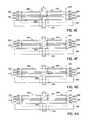
- FIG. 1Ais a plan view of an example of a first embodiment of a thin-film acoustically-coupled transformer in accordance with the invention
- FIGS. 1B and 1Care cross-sectional views of the thin-film acoustically-coupled transformer along section lines 1 B— 1 B and 1 C— 1 C, respectively, in FIG. 1 A.
- FIG. 1Dis an enlarged cross-sectional view of part of the acoustically-coupled transformer shown in FIG. 1A along the section line 1 B— 1 B showing a first embodiment of the acoustic decoupler.
- FIG. 1Eis an enlarged cross-sectional view of part of the acoustically-coupled transformer shown in FIG. 1A along the section line 1 B— 1 B showing a second embodiment of the acoustic decoupler.
- FIG. 2a graph showing how the calculated frequency response of embodiments of the thin-film acoustically-coupled transformer shown in FIGS. 1A-1C depends on the acoustic impedance of the acoustic decoupling material.
- FIG. 3Ais a plan view of an example of a second embodiment of a thin-film acoustically-coupled transformer in accordance with the invention
- FIGS. 3B and 3Care cross-sectional views of the thin-film acoustically-coupled transformer along section lines 3 B— 3 B and 3 C— 3 C, respectively, in FIG. 1 A.
- FIGS. 4A through 4Dare schematic drawings showing the electrical circuits of electrically balanced embodiments of the thin-film acoustically-coupled transformer shown in FIGS. 3A-3C .
- FIGS. 4E through 4Hare schematic drawings showing the electrical circuits of electrically unbalanced embodiments of the thin-film acoustically-coupled transformer shown in FIGS. 3A-3C .
- FIGS. 5A-5Jare plan views illustrating a process for making a thin-film acoustically-coupled transformer in accordance with the invention.
- FIGS. 5K-5Tare cross-sectional views along the section lines 5 K— 5 K, 5 L— 5 L, 5 M— 5 M, 5 N— 5 N, 5 O— 5 O, 5 P— 5 P, 5 Q— 5 Q, 5 R— 5 R, 5 S— 5 S and 5 T— 5 T in FIGS. 5A-5J , respectively.
- FIGS. 1A , 1 B and 1 Cshow a plan view and two cross-sectional views, respectively, of a first embodiment 100 of a thin-film acoustically-coupled transformer in accordance with the invention.
- Transformer 100has a 1:1 impedance transformation ratio, is capable of linking single-ended circuitry with balanced circuitry or vice versa and provides electrical isolation between primary and secondary.
- Transformer 100is composed of a stacked bulk acoustic resonator (SBAR) 106 , first terminals 132 and 134 and second terminals 136 and 138 .
- SBAR 106is composed of a stacked pair of film bulk acoustic resonators (FBARs) 110 and 120 and an acoustic decoupler 130 between them.
- FBAR 120is stacked atop FBAR 110 .
- FBAR 110is composed of opposed planar electrodes 112 and 114 and a layer of piezoelectric material 116 between the electrodes.
- FBAR 120is composed of opposed planar electrodes 122 and 124 and a layer of piezoelectric material 126 between the electrodes.
- Acoustic decoupler 130is located between electrode 114 of FBAR 110 and electrode 122 of FBAR 120 . The acoustic decoupler controls the coupling of acoustic energy between FBARs 110 and 120 .
- first terminals 132 and 134are structured as bonding pads electrically connected by electrical traces 133 and 135 , respectively, to electrodes 112 and 114 , respectively, of FBAR 110 .
- second terminals 136 and 138are structured as bonding pads electrically connected by electrical traces 137 and 139 , respectively, to electrodes 122 and 124 , respectively, of FBAR 120 .
- first terminals 132 and 134constitute the primary terminals and the second terminals 136 and 138 constitute the secondary terminals of thin-film acoustically-coupled transformer 100 .
- first terminals 132 and 134constitute the secondary terminals and second terminals 136 and 138 constitute the primary terminals of thin-film acoustically-coupled transformer 100 .
- SBAR 106is suspended over a cavity 104 defined in a substrate 102 . Suspending the SBAR over a cavity allows the FBARs of the SBAR to resonate mechanically. Other suspension schemes that allow the FBARs to resonate mechanically are possible.
- the SBARcan be located over a mismatched acoustic Bragg reflector (not shown) formed in or on substrate 102 , as disclosed by Lakin in U.S. Pat. No. 6,107,721, the disclosure of which is incorporated into this disclosure by reference.
- Ruby's disclosurealso discloses a stacked film bulk acoustic resonator (SBAR) composed of two layers of piezoelectric material interleaved with three planar electrodes.
- Ruby's SBARcan be regarded as being composed of a stacked pair of FBARs in which one electrode is common to both FBARs, and will be referred to as a common-electrode SBAR.
- the common electroderenders the common-electrode SBAR incapable of linking balanced to unbalanced circuits and vice versa and of providing electrical isolation between primary and secondary. Moreover, the common electrode SBAR exhibits an extremely narrow pass bandwidth that makes it unsuitable for use in most applications. The narrow pass bandwidth is the result of the common electrode, which over couples acoustic energy between the FBARs.
- acoustic decoupler 130controls the coupling of acoustic energy between stacked FBARs 110 and 120 and additionally electrically isolates FBAR 110 from FBAR 120 .
- the electrical isolation provided by acoustic decoupler 130enables transformer 100 to link balanced to unbalanced circuits and vice versa and provides electrical isolation between primary and secondary.
- the acoustic coupling provided by acoustic decoupler 130is substantially less than the acoustic coupling between the FBARs in the common electrode SBAR referred to above. As a result, FBARs 110 and 120 are not over coupled, and transformer 100 has a relatively flat response in the pass band, as will be described below with reference to FIG. 2 .
- the embodiment of the acoustic decoupler 130 shown in FIGS. 1A-1Cis a first embodiment composed of layer 131 of acoustic decoupling material located between the electrodes 114 and 122 of FBARs 110 and 120 , respectively.
- FIG. 1Dis an enlarged view showing this first embodiment of the acoustic decoupler in more detail.
- Important properties of the acoustic decoupling material of layer 131 that constitutes acoustic decoupler 130are an acoustic impedance less than that of the materials of FBARs 110 , 120 , a high electrical resistivity, a low dielectric permittivity and a nominal thickness that is an odd integral multiple of one quarter of the wavelength in the acoustic decoupling material of an acoustic wave having a frequency equal to the center frequency of the pass band of acoustically-coupled transformer 100 .
- the acoustic decoupling material of acoustic decoupler 130has an acoustic impedance less that of the materials of FBARs 110 and 120 and substantially greater than that of air.
- the acoustic impedance of a materialis the ratio of stress to particle velocity in the material and is measured in Rayleighs, abbreviated as rayl.
- the materials of the FBARsare typically aluminum nitride (AlN) as the material of piezoelectric layers 116 , 126 and molybdenum (Mo) as the material of electrodes 112 , 114 , 122 and 124 .
- the acoustic impedances of the materials of the FBARsare typically greater than 30 Mrayl (35 Mrayl for AlN and 63 Mrayl for Mo) and the acoustic impedance of air is about 1 krayl.
- materials with an acoustic impedance in the range from about 2 Mrayl to about 16 Mraylwork well as the acoustic coupling material of acoustic decoupler 130 .
- FIG. 2is a graph showing how the calculated frequency response of thin-film acoustically-coupled transformer 100 depends on the acoustic impedance of the acoustic decoupling material of layer 131 that constitutes the first embodiment of acoustic decoupler 130 .
- the embodiment illustratedhas a center frequency of about 1,900 MHz.
- Calculated frequency responses for embodiments in which the acoustic decoupling material of the acoustic decoupler has acoustic impedances of about 4 Mrayl (polyimide—curve 140 ), 8 Mrayl (curve 142 ) and 16 Mrayl (curve 144 )are shown.
- the bandwidth of transformer 100increases with increasing acoustic impedance of the acoustic decoupling material.
- the acoustic impedanceis 16 Mrayl
- the resonances of the FBARsare over coupled, which causes the characteristic double peak in the pass band response.
- acoustic decoupler 130 shown in FIGS. 1B , 1 C and 1 Dis composed of layer 131 of acoustic decoupling material with a nominal thickness equal to one quarter of the wavelength in the acoustic decoupling material of an acoustic wave having a frequency equal to the center frequency of the transformer's pass band, i.e., t ⁇ n /4, where t is the thickness of the layer 131 of acoustic decoupling material that constitutes acoustic decoupler 130 and ⁇ n is the wavelength in the acoustic decoupling material of an acoustic wave having a frequency equal to the center frequency of the pass band of transformer 100 .
- a thickness of layer 131 within approximately ⁇ 10% of the nominal thicknesscan alternatively be used. A thickness outside this range can alternatively be used with some degradation in performance. However, the thickness of layer 131 should differ significantly from 0 ⁇ n at one extreme and ⁇ n /2 at the other extreme.
- the first embodiment of acoustic decoupler 130 shown in FIG. 1Dis composed of layer 131 of acoustic decoupling material with a nominal thickness equal to an odd integral multiple of one quarter of the wavelength in the acoustic decoupling material of an acoustic wave having a frequency equal to the center frequency of the pass band of transformer 100 , i.e., t ⁇ (2m+1) ⁇ n /4, where t and ⁇ n are as defined above and m is an integer equal to or greater than zero.
- a thickness of layer 131 that differs from the nominal thickness by approximately ⁇ 10% of ⁇ n /4can alternatively be used. A thickness tolerance outside this range can be used with some degradation in performance, but the thickness of layer 131 should differ significantly from an integral multiple of ⁇ n /2.
- plastic materialshave acoustic impedances in the range stated above and can be applied in layers of uniform thickness in the thickness ranges stated above. Such plastic materials are therefore potentially suitable for use as the acoustic decoupling material of layer 131 of acoustic decoupler 130 .
- the acoustic decoupling materialmust also be capable of withstanding the temperatures of the fabrication operations performed after layer 131 of acoustic decoupling material has been deposited on electrode 114 to form acoustic decoupler 130 .
- electrodes 122 and 124 and piezoelectric layer 126are deposited by sputtering after layer 131 has been deposited. Temperatures as high as 300° C. are reached during these deposition processes. Thus, a plastic that remains stable at such temperatures is used as the acoustic decoupling material.
- Plastic materialstypically have a very high acoustical attenuation per unit length compared with the other materials of FBARs 110 and 120 .
- acoustic decoupler 130is composed of layer 131 of plastic acoustic decoupling material typically less than 1 ⁇ m thick, the acoustic attenuation introduced by layer 131 is typically negligible.
- a polyimideis used as the acoustic decoupling material of layer 131 .
- Polyimideis sold under the trademark Kapton® by E. I. du Pont de Nemours and Company.
- acoustic decoupler 130is composed of layer 131 of polyimide applied to electrode 114 by spin coating.
- Polyimidehas an acoustic impedance of about 4 Mrayl.
- a poly(para-xylylene)is used as the acoustic decoupling material of layer 131 .
- acoustic decoupler 130is composed of layer 131 of poly(para-xylylene) applied to electrode 114 by vacuum deposition.
- Poly(para-xylylene)is also known in the art as parylene.
- the dimer precursor di-para-xylylene from which parylene is made and equipment for performing vacuum deposition of layers of paryleneare available from many suppliers.
- Parylenehas an acoustic impedance of about 2.8 Mrayl.
- the acoustic decoupling material of layer 131 constituting acoustic decoupler 130has an acoustic impedance substantially greater than the materials of FBARs 110 and 120 . No materials having this property are known at this time, but such materials may become available in future, or lower acoustic impedance FBAR materials may become available in future.
- the thickness of layer 131 of such high acoustic impedance acoustic decoupling materialis as described above.
- FIG. 1Eis an enlarged view of part of thin-film acoustically-coupled transformer 100 showing a second embodiment of acoustic decoupler 130 that incorporates a Bragg structure 161 .
- Bragg structure 161is composed of a low acoustic impedance Bragg element 163 sandwiched between high acoustic impedance Bragg elements 165 and 167 .
- Low acoustic impedance Bragg element 163is a layer of a low acoustic impedance material whereas high acoustic impedance Bragg elements 165 and 167 are each a layer of high acoustic impedance material.
- the acoustic impedances of the Bragg elementsare characterized as “low” and “high” with respect to one another and additionally with respect to the acoustic impedance of the piezoelectric material of layers 116 and 126 . At least one of the Bragg elements additionally has a high electrical resistivity and a low dielectric permittivity to provide electrical isolation between input and output of transformer 100 .
- Each of the layers constituting Bragg elements 161 , 163 and 165has a nominal thickness equal to an odd integral multiple of one quarter of the wavelength in the material the layer of an acoustic wave having a frequency equal to the center frequency of transformer 100 .
- Layers that differ from the nominal thickness by approximately ⁇ 10% of one quarter of the wavelengthcan alternatively be used. A thickness tolerance outside this range can be used with some degradation in performance, but the thickness of the layers should differ significantly from an integral multiple of one-half of the wavelength.
- low acoustic impedance Bragg element 163is a layer of silicon dioxide (SiO 2 ), which has an acoustic impedance of about 13 Mrayl
- each of the high acoustic impedance Bragg elements 165 and 167is a layer of the same material as electrodes 114 and 122 , respectively, i.e., molybdenum, which has an acoustic impedance of about 63 Mrayl.
- high acoustic impedance Bragg elements 165 and 167 and electrodes 114 and 122 , respectively, of FBARs 110 and 120 , respectively,allows high acoustic impedance Bragg elements 165 and 167 additionally to serve as electrodes 114 and 122 , respectively.
- high acoustic impedance Bragg elements 165 and 167have a nominal thickness equal to one quarter of the wavelength in molybdenum of an acoustic wave having a frequency equal to the center frequency of the pass band of transformer 100
- low acoustic impedance Bragg element 163had a nominal thickness equal to three quarters of the wavelength in SiO 2 of an acoustic wave having a frequency equal to the center frequency of the pass band of the transformer.
- Using a three-quarter wavelength-thick layer of SiO 2 instead of a one-quarter wavelength thick layer of SiO 2 as low acoustic impedance Bragg element 163reduces the capacitance between FBARs 110 and 120 .
- Bragg structure 161may be composed of more than one (e.g., n) low acoustic impedance Bragg element interleaved with a corresponding number (i.e., n+1) of high acoustic impedance Bragg elements. Only one of the Bragg elements need be insulating.
- the Bragg structuremay be composed of two low acoustic impedance Bragg element interleaved with three high acoustic impedance Bragg elements.
- Wafer-scale fabricationis used to fabricate thin-film acoustically-coupled transformers similar to thin-film acoustically-coupled transformer 100 thousands at a time. Wafer-scale fabrication makes each thin-film acoustically-coupled transformer inexpensive to fabricate. Thin-film acoustically-coupled transformer 100 can be made using a fabrication method similar to that to be described below with reference to FIGS. 5A-5T . Accordingly, a method of fabricating thin-film acoustically-coupled transformer 100 will not be separately described.
- first terminals 132 and 134electrically connected to electrodes 112 and 114 , respectively, as shown in FIGS. 1A and 1B and electrical connections are additionally made to second terminals 136 and 138 electrically connected to electrodes 122 and 124 , respectively, as shown in FIGS. 1A and 1C .
- the electrical connections to first terminals 132 and 134provide electrical connections to the primary of thin-film acoustically-coupled transformer 100 and the electrical connections to second terminals 136 and 138 provide electrical connections to the secondary of thin-film acoustically-coupled transformer 100 .
- the electrical connections to second terminals 136 and 138provide electrical connections to the primary of thin-film acoustically-coupled transformer 100 and the electrical connections to first terminals 132 and 134 provide electrical connections to the secondary of thin-film acoustically-coupled transformer 100 .
- an input electrical signal applied to first terminals 132 and 134which constitute the primary terminals of thin-film acoustically-coupled transformer 100 , establishes a voltage difference between electrodes 112 and 114 of FBAR 110 .
- the voltage difference between electrodes 112 and 114mechanically deforms FBAR 110 at the frequency of the input electrical signal.
- acoustic decoupler 130couples all or part of the acoustic energy resulting from the mechanical deformation of FBAR 110 to FBAR 120 .
- the acoustic energy received from FBAR 110mechanically deforms FBAR 120 at the frequency of the input electrical signal.
- FBAR 120The mechanical deformation of FBAR 120 generates a voltage difference between electrodes 122 and 124 at the frequency of the input electrical signal.
- the voltage differenceis output at second terminals 136 and 138 , which constitute the secondary terminals of transformer 100 , as an output electrical signal.
- Piezoelectricityis a linear effect, so the amplitude and phase of the input electrical signal applied to the first terminals is preserved in the output electrical signal output at the second terminals.
- An embodiment of thin-film acoustically-coupled transformer 100 in which second terminals 136 and 138 constitute the primary terminals and first terminals 132 and 134 constitute the secondary terminalsoperates similarly, except acoustic energy propagates through acoustic decoupler 130 from FBAR 120 to FBAR 110 .
- thin-film acoustically-coupled transformer 100provides a 1:1 impedance transformation ratio, is capable of linking single-ended circuitry with balanced circuitry or vice versa and provides electrical isolation between primary and secondary.
- the capacitance between electrode 112 and substrate 102differs from that between electrode 114 and the substrate.
- thin-film acoustically-coupled transformer 100is not perfectly balanced electrically and can have an insufficient common-mode rejection ratio (CMRR) for certain applications.
- CMRRcommon-mode rejection ratio
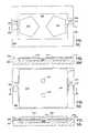
- FIGS. 3A-3Cshow a plan view and two cross-sectional views, respectively, of a second embodiment 200 of a thin-film acoustically-coupled transformer in accordance with the invention.
- Acoustically-coupled transformer 200is capable of linking single-ended circuitry with balanced circuitry or vice versa, provides electrical isolation between primary and secondary. Some embodiments of transformer 200 are electrically balanced, and therefore have a high common-mode rejection ratio: other embodiments are electrically unbalanced and have a lower common-mode rejection ratio. Acoustically-coupled transformer 200 has an impedance transformation ratio of 1:1, 1:4 or 4:1 depending on the configurations of the electrical circuits that form part of the transformer.
- Acoustically-coupled transformer 200is composed of two stacked bulk acoustic resonators (SBARs) 206 and 208 .
- SBARsbulk acoustic resonators
- Each SBARis composed of a stacked pair of film bulk acoustic resonators (FBARs) and an acoustic decoupler between the FBARs.
- Transformer 200is additionally composed of an electrical circuit that connects one of the FBARs of SBAR 206 to one of the FBARs of SBAR 208 , and an electrical circuit that connects the other of the FBARs of SBAR 206 to the other of the FBARs of SBAR 208 .
- SBAR 206is composed of a stacked pair of FBARs 210 and 220 and an acoustic decoupler 230 between them.
- SBAR 208is composed of a stacked pair of FBARs 250 and 260 and an acoustic decoupler 270 between them.
- FBAR 220is stacked atop FBAR 210 and FBAR 260 is stacked atop FBAR 250 .
- FBAR 210is composed of opposed planar electrodes 212 and 214 and a layer of piezoelectric material 216 between the electrodes.
- FBAR 220is composed of opposed planar electrodes 222 and 224 and a layer of piezoelectric material 226 between the electrodes.
- FBAR 250is composed of opposed planar electrodes 252 and 254 and a layer of piezoelectric material 256 between the electrodes.
- FBAR 260is composed of opposed planar electrodes 262 and 264 and a layer of piezoelectric material 266 between the electrodes.
- an electrical circuitconnects one of the FBARs of SBAR 206 to one of the FBARs of SBAR 208 , and an electrical circuit connects the other of the FBARs of SBAR 206 to the other of the FBARs of SBAR 206 .
- Each electrical circuitelectrically connects the respective FBARs in any one of a parallel, a series, an anti-parallel and an anti-series configuration. Of the sixteen possible combinations of the parallel, series, anti-parallel and anti-series electrical circuit configurations, only eight produce a working transformer.
- the combination of electrical circuit configurations connecting the FBARsdetermines whether the transformer is electrically balanced (high common-mode rejection ratio) or electrically unbalanced, and determines the impedance transformation ratio of the transformer, i.e., 1:1, 1:4 or 4:1.
- the possible combinations of electrical circuit configurationsare summarized in Table 1 below:
- the row captionsindicate the configuration of one of the electrical circuits, e.g., electrical circuit 245 described below with reference to FIG. 4C
- the column captionsindicate the configuration of the other of the electrical circuits, e.g., electrical circuit 246 described with reference to FIG. 4C
- Bdenotes that the transformer is electrically balanced
- Udenotes that the transformer is unbalanced
- Xdenotes a non-functioning transformer.
- the impedance transformation ratio shownis the impedance transformation from electrical terminals connected to the electrical circuit indicated by the row caption to electrical terminals connected to the electrical circuit indicated by the column caption.
- the electrical circuits shown in Table 1are subject to the constraint that an electrical circuit may only connect the electrodes of FBARs at the same level as one another in SBARs 206 and 208 , i.e., one of the electrical circuits may only connect the electrodes of FBARs 210 and 250 and the other of the electrical circuits may only connect the electrodes of FBARs 220 and 260 .
- Table 1additionally assumes that the c-axes of piezoelectric layers 216 , 226 , 256 and 266 are all oriented in the same direction.
- More electrical circuitsare possible in embodiments not subject to the constraint, e.g., in embodiments in which an electrical circuit is allowed to connect the electrodes of FBARs 210 and 260 and the electrodes of FBARs 220 and 250 , and/or the assumption.
- An FBARis a polarity-dependent device. A voltage of a given polarity applied between the electrodes of the FBAR will cause the FBAR to contract mechanically while the same voltage of the opposite polarity will cause the FBAR to expand mechanically by the same amount.
- a mechanical stress applied to the FBAR that causes the FBAR to contract mechanicallywill generate a voltage of the given polarity between the electrodes of the FBAR whereas a mechanical stress that causes the FBAR to expand mechanically will generate a voltage of the opposite polarity between the electrodes of the FBAR.
- the electrodes of the FBARs that an electrical circuit connects in parallelare at the same level in the respective SBARs.
- a signal applied to the FBARs connected in parallelproduces signals of the same phase across the FBARs.
- the FBARstherefore expand and contract in phase, and generate acoustic energy in phase.
- electrodes of the FBARs that an electrical circuit connects in anti-parallelare at different levels in the respective SBARs.
- a signal applied to FBARs connected in anti-parallelproduces signals of the opposite phases across the FBARs. The FBARs therefore expand and contract in antiphase, and generate acoustic energy in antiphase.
- the electrodes of the FBARs that an electrical circuit connects in seriesare at the same level in the respective SBARs.
- a signal applied to the FBARs connected in seriesproduces signals of opposite phases across the FBARs.
- the FBARsexpand and contract in antiphase, and generate acoustic energy in antiphase.
- the electrodes of the FBARs that an electrical circuit connects in anti-seriesare at different levels in the respective SBARs.
- a signal applied to the FBARs connected in anti-seriesproduces signals of the same phase across the FBARs.
- the FBARsexpand and contract in phase and generate acoustic energy in phase.
- FBARs receiving acoustic energy that causes them to expand and contract in phasegenerate signals in phase.
- Connecting FBARs that generate signals in phase in parallelproduces a signal level equal to that across the individual FBARs and an impedance of one-half the characteristic impedance of the individual FBARs.
- Connecting such FBARs in anti-seriesproduces a signal level of twice that across the individual FBARs and an impedance of twice the characteristic impedance of the individual FBARs.
- connecting FBARs that generate signals in phase in anti-parallel or in seriescauses the signals to cancel.
- FBARs receiving acoustic energy that causes them to expand and contract in antiphasegenerate signals in antiphase.
- Connecting FBARs that generate signals in antiphase in antiparallelproduces a signal equal in level to that across the individual FBARs and an impedance of one-half the characteristic impedance of the individual FBARs. Connecting such FBARs in series produces a signal of twice the level of that across the individual FBARs and an impedance of twice the characteristic impedance of the individual FBARs. However, connecting FBARs that generate signals in antiphase in parallel or in antiseries causes the signals to cancel.
- the transformers indicated in Table 1 as being non-functionalare transformers in which the FBARs that receive acoustic energy generate signals that cancel.
- FIGS. 4A and 4Bschematically illustrate two configurations of electrical circuits that connect the FBARs 210 and 220 of SBAR 206 and the FBARs 250 and 260 of SBAR 208 in anti-parallel or in series, respectively, to form respective electrically-balanced embodiments of an acoustically-coupled transformer having a 1:1 impedance transformation ratio.
- FIG. 4Ashows an electrical circuit 241 electrically connecting one of the FBARs of SBAR 206 in anti-parallel with one of the FBARs of SBAR 208 and to first terminals F and an electrical circuit 242 electrically connecting the other of the FBARs of SBAR 206 in anti-parallel with the other of the FBARs of SBAR 208 and to second terminals S.
- the electrical circuit 241electrically connects FBAR 220 of SBAR 206 in anti-parallel with FBAR 260 of SBAR 208 and to first terminals F
- electrical circuit 242electrically connects FBAR 210 of SBAR 206 in anti-parallel with FBAR 250 of SBAR 208 and to second terminals S.
- electrical circuit 241electrically connects electrode 222 of FBAR 220 to electrode 264 of FBAR 260 and to one of the first terminals F and additionally electrically connects electrode 224 of FBAR 220 to electrode 262 of FBAR 260 and to the other of the first terminals F.
- Electrical circuit 242electrically connects electrode 214 of FBAR 210 to electrode 252 of FBAR 250 and to one of the second terminals S and additionally electrically connects electrode 212 of FBAR 210 to electrode 254 of FBAR 250 and to the other of the second terminals S.
- Electrical circuit 241electrically connects FBARs 220 and 260 in anti-parallel so that an input electrical signal applied to the first terminals F is applied equally but in antiphase to FBARs 220 and 260 . Electrical circuit 241 electrically connects FBARs 220 and 260 in anti-parallel in the sense that an electrical signal applied to first terminals F that causes FBAR 220 to contract mechanically additionally causes FBAR 260 to expand mechanically by the same amount, and vice versa. The acoustic energy generated by FBAR 260 is therefore in antiphase with the acoustic energy generated by FBAR 220 .
- the acoustic energy received by FBAR 250 from FBAR 260is in antiphase with the acoustic energy received by FBAR 210 from FBAR 220 , and the signal between electrodes 214 and 212 is in antiphase with the signal between electrodes 254 and 252 .
- Electrical circuit 242connects FBARs 210 and 250 in anti-parallel, so that the signal output to the second terminals S is in phase with the signal between electrodes 214 and 212 and also with the signal between electrodes 254 and 252 .
- the signal between second terminals Sis the same as the signal across either of FBARs 210 and 250 .
- Each first terminalhas connected to it one electrode closer to the substrate and one electrode further from the substrate.
- one first terminalhas electrode 222 closer to the substrate and electrode 264 further from the substrate connected to it and the other first terminal has electrode 262 closer to the substrate and electrode 224 further from the substrate connected to it.
- substantially the same capacitanceexists between each of the second terminals S and substrate 202 .
- Each second terminalhas connected to it one electrode closer to the substrate and one electrode further from the substrate.
- one second terminalhas electrode 212 closer to the substrate and electrode 254 further from the substrate connected to it and the other second terminal has electrode 252 closer to the substrate and electrode 214 further from the substrate connected to it.
- the embodiment of thin-film acoustically-coupled transformer 200 shown in FIG. 4Ais electrically balanced and, as a result, has a common-mode rejection ratio sufficiently high for many more applications than the thin-film acoustically-coupled transformer 100 described above with reference to FIGS. 1A-1C .
- the embodiment of thin-film acoustically-coupled transformer 200 shown in FIG. 4Ahas a 1:1 impedance transformation ratio.
- First terminals Fmay serve as the primary terminals or the secondary terminals of the transformer and second terminals P may serve as the secondary terminals or the primary terminals, respectively, of the transformer.
- An input electrical signal applied to the primary terminalsis output at substantially the same level at the secondary terminals.
- the impedance seen at the primary terminals and at the secondary terminalsis that of two FBARs in parallel, i.e., one half of the typical characteristic impedance of a single FBAR.
- the embodiment of thin-film acoustically-coupled transformer 200 shown in FIG. 4Ais suitable for use in relatively low characteristic impedance applications.
- FIG. 4Bschematically shows an electrical circuit 243 electrically connecting one of the FBARs of SBAR 206 and one of the FBARs of SBAR 208 in series between first terminals F and an electrical circuit 244 electrically connecting the other of the FBARs of SBAR 206 and the other of the FBARs of SBAR 208 in series between second terminals S.
- electrical circuit 243electrically connects FBAR 220 of SBAR 206 and FBAR 260 of SBAR 208 in series between first terminals F
- electrical circuit 244electrically connects FBAR 210 of SBAR 206 and FBAR 250 of SBAR 208 in series between second terminals S.
- electrical circuit 243electrically connects electrode 222 of FBAR 220 to electrode 262 of FBAR 260 and additionally electrically connects electrode 224 of FBAR 220 to one of the first terminals F and electrically connects electrode 264 of FBAR 260 to the other of the first terminals F.
- electrical circuit 243electrically connects electrode 224 of FBAR 220 to electrode 264 of FBAR 260 and additionally electrically connects electrode 222 of FBAR 220 and electrode 262 of FBAR 260 to first terminals F.
- Electrical circuit 244electrically connects electrode 212 of FBAR 210 to electrode 252 of FBAR 250 and additionally electrically connects electrode 214 of FBAR 210 to one of the second terminals S and additionally electrically connects electrode 254 of FBAR 250 to the other of the second terminals S.
- electrical circuit 244electrically connects electrode 214 of FBAR 210 to electrode 254 of FBAR 250 and additionally electrically connects electrode 212 of FBAR 210 and electrode 252 of FBAR 250 to second terminals S.
- Electrical circuit 243 electrically connecting FBARs 220 and 260 in seriesdivides an input electrical signal applied to the first terminals F approximately equally between FBARs 220 and 260 .
- FBARs 220 and 260are connected in series in the sense that an electrical signal applied to first terminals F that causes FBAR 220 to contract mechanically causes FBAR 260 to expand mechanically by the same amount, and vice versa.
- the acoustic energy generated by FBAR 260is therefore in antiphase with the acoustic energy generated by FBAR 220 .
- the acoustic energy received by FBAR 250 from FBAR 260is in antiphase with the acoustic energy received by FBAR 210 from FBAR 220 and the signal on electrode 254 is in antiphase with the signal on electrode 214 .
- Electrical circuit 244electrically connects FBARs 210 and 250 in series so that the signal at second terminals S is twice the signal across either of FBARs 210 and 250 .
- Electrodes 224 and 264 connected to the first terminalsare at the same distance from the substrate.
- substantially the same capacitanceexists between each of the second terminals S and substrate 202 .
- Electrodes 214 and 254 connected to the second terminalsare at the same distance from the substrate.
- the embodiment of thin-film acoustically-coupled transformer 200 shown in FIG. 4Bhas a 1:1 impedance transformation ratio.
- First terminals Fmay serve as the primary terminals or the secondary terminals of the transformer and second terminals P may serve as the secondary terminals or the primary terminals, respectively, of the transformer.
- An input electrical signal applied to the primary terminalsis output at substantially the same level at the secondary terminals.
- the impedance seen at the primary terminals and at the secondary terminalsis that of two FBARs in series, i.e., twice the typical characteristic impedance of a single FBAR.
- the embodiment of thin-film acoustically-coupled transformer 200 shown in FIG. 4Bis suitable for use in higher characteristic impedance applications than that shown in FIG. 4 A.
- FIGS. 4C and 4Dschematically illustrate two configurations of electrical circuits that connect the FBARs 210 and 220 of SBAR 206 and the FBARs 250 and 260 of SBAR 208 in anti-parallel and in series to form respective embodiments of an acoustically-coupled transformer having a 1:4 or 4:1 impedance transformation ratio.
- FIG. 4Cshows an electrical circuit 245 electrically connecting one of the FBARs of SBAR 206 in anti-parallel with one of the FBARs of SBAR 208 and to first terminals F and an electrical circuit 246 electrically connecting the other of the FBARs of SBAR 206 and the other of the FBARs of SBAR 208 in series between second terminals S.
- the electrical circuit 245electrically connects FBAR 220 of SBAR 206 in anti-parallel with FBAR 260 of SBAR 208 and to first terminals P, and electrical circuit 246 electrically connects FBAR 210 of SBAR 206 and FBAR 250 of SBAR 208 in series between second terminals S.
- electrical circuit 245electrically connects electrode 222 of FBAR 220 to electrode 264 of FBAR 260 and to one of the first terminals F, and additionally electrically connects electrode 224 of FBAR 220 to electrode 262 of FBAR 260 and to the other of the first terminals F.
- Electrical circuit 246electrically connects electrode 214 of FBAR 210 to electrode 254 of FBAR 250 and additionally electrically connects electrode 212 of FBAR 210 to one of the second terminals S and electrode 252 of FBAR 250 to the other of the second terminals S.
- electrical circuit 246electrically connects electrode 212 of FBAR 210 to electrode 252 of FBAR 250 and additionally electrically connects electrode 214 of FBAR 210 and electrode 254 of FBAR 250 to second terminals S.
- Electrical circuit 245electrically connects FBARs 220 and 260 in anti-parallel so that an input electrical signal applied to the first terminals F is applied equally but in antiphase to FBARs 220 and 260 .
- Electrical circuit 245electrically connects FBARs 220 and 260 in anti-parallel in the sense that an electrical signal applied to first terminals F that causes FBAR 220 to contract mechanically additionally causes FBAR 260 to expand mechanically by the same amount, and vice versa.
- the acoustic energy generated by FBAR 260is therefore in antiphase with the acoustic energy generated by FBAR 220 .
- the acoustic energy received by FBAR 250 from FBAR 260is in antiphase with the acoustic energy received by FBAR 210 from FBAR 220 , and the signal on electrode 252 is in antiphase with the signal on electrode 212 .
- Electrical circuit 246connects FBARs 210 and 250 in series so that the voltage difference between second terminals S is twice the voltage across either of FBARs 210 and 250 .
- each first terminalhas connected to it one electrode closer to the substrate and one electrode further from the substrate.
- one first terminalhas electrode 222 closer to the substrate and electrode 264 further from the substrate connected to it and the other first terminal has electrode 262 closer to the substrate and electrode 224 further from the substrate connected to it.
- substantially the same capacitanceexists between each of the second terminals S and substrate 202 . Electrodes 212 and 252 connected to the second terminals are at the same distance from the substrate.
- the embodiment of thin-film acoustically-coupled transformer 200 shown in FIG. 4Cis electrically balanced and, as a result, has a common-mode rejection ratio sufficiently high for many more applications than the thin-film acoustically-coupled transformer 100 described above with reference to FIGS. 1A-1C .
- the embodiment of thin-film acoustically-coupled transformer 200 shown in FIG. 4Cis a step-up transformer when first terminals F serve as primary terminals and second terminals S serve as secondary terminals. A signal applied to the primary terminals is output at twice the level at the secondary terminals.
- the impedance seen at the primary terminalsis that of two FBARs in parallel, i.e., one half of the typical characteristic impedance of a single FBAR, whereas the impedance seen at the secondary terminals is that of two FBARs in series, i.e., twice the typical characteristic impedance of a single FBAR.
- the embodiment of thin-film acoustically-coupled transformer 200 illustrated in FIG. 4Chas a 1:4 primary-to-secondary impedance ratio.
- the embodiment of thin-film acoustically-coupled transformer 200 shown in FIG. 4Cis a step-down transformer when first terminals F serve as secondary terminals and second terminals S serve as primary terminals.
- the signal output at the secondary terminalsis one-half the level of the input electrical signal applied to the primary terminals, and the primary-to-secondary impedance ratio is 4:1.
- FIG. 4Dschematically shows an electrical circuit 247 electrically connecting FBAR 220 of SBAR 206 and FBAR 260 of SBAR 208 in series between first terminals F, and an electrical circuit 248 electrically connecting FBAR 210 of SBAR 206 and FBAR 250 of SBAR 208 in anti-parallel and to second terminals S.
- electrical circuit 247electrically connects electrode 222 of FBAR 220 to electrode 262 of FBAR 260 and additionally electrically connects electrode 224 of FBAR 220 and electrode 264 of FBAR 260 to first terminals F.
- Electrical circuit 248electrically connects electrode 212 of FBAR 210 to electrode 254 of FBAR 250 and to one of the second terminals S, and additionally electrically connects electrode 214 of FBAR 210 to electrode 252 of FBAR 250 and to the other of the second terminals S.
- electrical circuit 247electrically connects electrode 224 of FBAR 220 to electrode 264 of FBAR 260 and additionally electrically connects electrode 222 of FBAR 220 and electrode 262 of FBAR 260 to first terminals F.
- Electrical circuit 247 electrically connecting FBARs 220 and 260 in seriesdivides an input electrical signal applied to the first terminals F approximately equally between FBARs 220 and 260 .
- FBARs 220 and 260are connected in series in the sense that an electrical signal applied to first terminals F that causes FBAR 220 to contract mechanically causes FBAR 260 to expand mechanically by the same amount, and vice versa.
- the acoustic energy generated by FBAR 260is therefore in antiphase with the acoustic energy generated by FBAR 220 .
- the acoustic energy received by FBAR 250 from FBAR 260is in antiphase with the acoustic energy received by FBAR 210 from FBAR 220 and the voltage between electrodes 252 and 254 is in antiphase with the voltage between electrodes 212 and 214 .
- Electrical circuit 248electrically connects FBARs 210 and 250 in anti-parallel, so that the signal output at the second terminals S is in phase with the signal across electrodes 214 and 212 and also with the signal across electrodes 254 and 252 .
- the signal at second terminals Sis equal in level to the signal across either of FBARs 210 and 250 , and is equal to one-half the level of the input electrical signal applied to first terminals F.
- Electrodes 224 and 264 connected to the first terminalsare the at same distance from the substrate.
- substantially the same capacitanceexists between each of the second terminals S and substrate 202 .
- Each second terminalhas connected to it one electrode closer to the substrate and one electrode further from the substrate.
- one second terminalhas electrode 212 closer to the substrate and electrode 254 further from the substrate connected to it and the other second terminal has electrode 252 closer to the substrate and electrode 214 further from the substrate connected to it.
- the embodiment of thin-film acoustically-coupled transformer 200 shown in FIG. 4Dis electrically balanced and, as a result, has a common-mode rejection ratio sufficiently high for many more applications than the thin-film acoustically-coupled transformer 100 described above with reference to FIGS. 1A-1C .
- the embodiment of thin-film acoustically-coupled transformer 200 shown in FIG. 4Dis a step-down transformer when first terminals F serve as primary terminals and second terminals S serve as secondary terminals.
- the signal level output at the secondary terminalsis one-half that of the input electrical signal applied to the primary terminals.
- the impedance seen at the primary terminalsis that of two FBARs in series, i.e., twice the typical characteristic impedance of a single FBAR, whereas the impedance seen at the secondary terminals is that of two FBARs in parallel, i.e., one-half of the typical characteristic impedance of a single FBAR.
- the embodiment of thin-film acoustically-coupled transformer 200 illustrated in FIG. 4Dhas a 4:1 primary-to-secondary impedance ratio.
- the embodiment of thin-film acoustically-coupled transformer 200 shown in FIG. 4Dis a step-up transformer when first terminals F serve as secondary terminals and second terminals S serve as primary terminals.
- the signal level output at the secondary terminalsis twice that of the input electrical signal applied to the primary terminals, and the primary-to-secondary impedance ratio is 1:4.
- FIG. 4Eshows an embodiment of an acoustically-coupled transformer with a 1:1 impedance transformation ratio in which an electrical circuit 341 connects FBAR 220 of SBAR 206 and FBAR 260 of SBAR 208 in parallel and to first terminals F, and an electrical circuit 342 electrically connects FBAR 210 of SBAR 206 and FBAR 250 of SBAR 208 in parallel and to second terminals S.
- FIG. 4Fshows an embodiment of an acoustically-coupled transformer with a 1:1 impedance transformation ratio in which an electrical circuit 343 connects FBAR 220 of SBAR 206 and FBAR 260 of SBAR 208 in anti-series between first terminals F, and an electrical circuit 344 connects FBAR 210 of SBAR 206 and FBAR 250 of SBAR 208 in anti-series between second terminals S.
- FIG. 4Gshows an embodiment of an acoustically-coupled transformer in which an electrical circuit 345 electrically connects FBAR 220 of SBAR 206 and FBAR 260 of SBAR 208 in parallel and to first terminals F, and an electrical circuit 346 electrically connects FBAR 210 of SBAR 206 and FBAR 250 of SBAR 208 in anti-series between second terminals S.
- This embodimenthas a 1:4 impedance transformation ratio when first terminals F serve as primary terminals and second terminals S serve as secondary terminals, or a 4:1 impedance transformation ratio when second terminals S serve as the primary terminals and first terminals F serve as the secondary terminals.
- FIG. 4Hshows an embodiment of an acoustically-coupled transformer in which electrical circuit 347 electrically connects FBAR 220 of SBAR 206 and FBAR 260 of SBAR 208 in anti-series between first terminals F, and an electrical circuit 348 electrically connects FBAR 210 of SBAR 206 and FBAR 250 of SBAR 208 in parallel and to second terminals S.
- This embodimenthas a 4:1 impedance transformation ratio when first terminals F serve as primary terminals and second terminals S serve as secondary terminals, or a 1:4 impedance transformation ratio when second terminals S serve as the primary terminals and first terminals F serve as the secondary terminals.
- the electrical configuration of the embodiment of the thin-film acoustically-coupled transformer 200 shown in FIGS. 3A-3Cis similar to that shown in FIG. 4C.
- a bonding pad 282 and a bonding pad 284constitute the first terminals of thin-film acoustically-coupled transformer 200 .
- An interconnection pad 236 , an electrical trace 237 extending from electrode 222 to interconnection pad 236 (FIG. 5 G), an interconnection pad 278 in electrical contact with interconnection pad 236 and an electrical trace 279 extending from electrode 264 to interconnection pad 278constitute the part of electrical circuit 245 ( FIG. 4C ) that electrically connects electrode 222 of FBAR 220 to electrode 264 of FBAR 260 .
- An interconnection pad 238 , an electrical trace 239 extending from electrode 224 to interconnection pad 238 , an interconnection pad 276 in electrical contact with interconnection pad 238 and an electrical trace 277 extending from electrode 262 to interconnection pad 276constitute the part of electrical circuit 245 ( FIG. 4C ) that electrically connects electrode 224 of FBAR 220 to electrode 262 of FBAR 260 .
- An electrical trace 283 that extends between electrode 222 and bonding pad 282 and an electrical trace 285 that extends between electrode 264 and bonding pad 284 ( FIG. 5G )constitute the part of electrical circuit 245 that connects FBARs 220 and 260 connected in anti-parallel to the first terminals provided by bonding pads 282 and 284 .
- bonding pads 282 and 284 and traces 283 and 285are omitted and interconnection pads 238 and 278 are configured as bonding pads and provide the first terminals of thin-film acoustically-coupled transformer 200 .
- Bonding pad 232 and bonding pad 272constitute the second terminals of thin-film acoustically-coupled transformer 200 .
- An electrical trace 235 that extends between electrode 214 and electrode 254 ( FIG. 5E )constitutes the part of electrical circuit 246 ( FIG. 4C ) that connects FBAR 210 and FBAR 250 in series.
- An electrical trace 233 that extends between electrode 212 and bonding pad 232 and an electrical trace 273 that extends between electrode 252 and bonding pad 272 ( FIG. 5C )constitutes the part of electrical circuit 246 that connects FBAR 210 and FBAR 250 to the second terminals provided by bonding pads 232 and 272 .
- acoustic decoupler 230is located between FBARs 210 and 220 , specifically, between electrodes 214 and 222 . Acoustic decoupler 230 controls the coupling of acoustic energy between FBARs 210 and 220 . Additionally, acoustic decoupler 270 is located between FBARs 250 and 260 , specifically, between electrodes 254 and 262 . Acoustic decoupler 270 controls the coupling of acoustic energy between FBARs 250 and 260 . Acoustic decoupler 230 couples less acoustic energy between the FBARs 210 and 220 than would be coupled if the FBARs were in direct contact with one another.
- Acoustic decoupler 270couples less acoustic energy between the FBARs 250 and 260 than would be coupled if the FBARs were in direct contact with one another.
- the coupling of acoustic energy defined by acoustic decouplers 230 and 270determines the pass bandwidth of thin-film acoustically-coupled transformer 200 .
- acoustic decouplers 230 and 270are respective parts of a layer 231 of acoustic decoupling material.
- Important properties of the acoustic decoupling material of layer 231are an acoustic impedance less than that of FBARs 210 , 220 , 250 and 260 , a nominal thickness that is an odd integral multiple of one quarter of the wavelength in the acoustic decoupling material of an acoustic wave having a frequency equal to the center frequency of the pass band of the transformer 200 , and a high electrical resistivity and low dielectric permittivity to provide electrical isolation between the primary and secondary of the transformer.
- acoustic decouplers 230 and 270each include a Bragg structure similar to Bragg structure 161 described above with reference to FIG. 1 E. Acoustic decouplers 230 and 270 may alternatively share a common Bragg structure in a manner similar to the way in which the embodiments of acoustic couplers 230 and 270 shown in FIGS. 3A-3C share a common layer 231 .
- SBAR 206 and SBARs 208are located adjacent one another suspended over a cavity 204 defined in a substrate 202 . Suspending the SBARs over a cavity allows the stacked FBARs in each SBAR to resonate mechanically. Other suspension schemes that allow the stacked FBARs to resonate mechanically are possible.
- the SBARscan be located over a mismatched acoustic Bragg reflector (not shown) formed in or on substrate 202 , as disclosed by the above-mentioned U.S. Pat. No. 6,107,721 of Lakin.
- Thousands of thin-film acoustically-coupled transformers similar to thin-film acoustically-coupled transformer 200are fabricated at a time by wafer-scale fabrication. Such wafer-scale fabrication makes the thin-film acoustically-coupled transformers inexpensive to fabricate.
- An exemplary fabrication methodwill be described next with reference to the plan views of FIGS. 5A-5J and the cross-sectional views of FIGS. 5K-5T . As noted above, the fabrication method can also be used to make the thin-film acoustically-coupled transformer 100 described above with reference to FIGS. 1A-1C .
- FIGS. 5A-5J and FIGS. 5K-5Tillustrate and the following description describes the fabrication of transformer 200 in and on a portion of the wafer. As transformer 200 is fabricated, the remaining transformers on the wafer are similarly fabricated.
- the portion of the wafer that constitutes substrate 202 of transformer 200is selectively wet etched to form cavity 204 , as shown in FIGS. 5A and 5K .
- FIGS. 5B and 5Lshow cavity 204 in substrate 202 filled with fill material 205 .
- the fill materialwas phosphosilicate glass (PSG) and was deposited using conventional low-pressure chemical vapor deposition (LPCVD).
- the fill materialmay alternatively be deposited by sputtering, or by spin coating.
- a layer of metalis deposited on the surface of the wafer and the fill material.
- the metalis patterned to define electrode 212 , bonding pad 232 , an electrical trace 233 extending between electrode 212 and bonding pad 232 , electrode 252 , bonding pad 272 and an electrical trace 273 extending between electrode 212 and bonding pad 272 , as shown in FIGS. 5C and 5M .
- Electrode 212 and electrode 252typically have an irregular shape in a plane parallel to the major surface of the wafer. An irregular shape minimizes lateral modes in FBAR 210 and FBAR 250 ( FIG. 3A ) of which the electrodes form part, as described in U.S. Pat. No.
- Electrode 212 and electrode 252are located to expose part of the surface of fill material 205 so that the fill material can later be removed by etching, as will be described below.
- electrodes 212 , 214 , 222 , 224 , 252 , 254 , 262 and 264are defined are patterned such that, in respective planes parallel to the major surface of the wafer, electrodes 212 and 214 of FBAR 210 have the same shape, size, orientation and position, electrodes 222 and 224 of FBAR 220 have the same shape, size, orientation and position, electrodes 252 and 254 of FBAR 250 have the same shape, size, orientation and position and electrodes 262 and 264 of FBAR 260 have the same shape, size, orientation and position.
- electrodes 214 and 222additionally have the same shape, size, orientation and position and electrodes 254 and 262 additionally have the same shape, size, orientation and position.
- the metal deposited to form electrode 212 , bonding pad 232 , trace 233 , electrode 252 , bonding pad 272 and trace 273was molybdenum.
- the molybdenumwas deposited with a thickness of about 440 nm by sputtering, and was patterned by dry etching to define pentagonal electrodes each with an area of about 26,000 square ⁇ m.
- Other refractory metalssuch as tungsten, niobium and titanium may alternatively be used as the material of electrodes 212 and 252 , bonding pads 232 and 272 and traces 233 and 273 .
- the electrodes, bonding pads and tracesmay alternatively comprise layers of more than one material.
- a layer of piezoelectric materialis deposited and is patterned to define a piezoelectric layer 217 that provides piezoelectric layer 216 of FBAR 210 and piezoelectric layer 256 of FBAR 250 , as shown in FIGS. 5D and 5N .
- Piezoelectric layer 217is patterned to expose part of the surface of fill material 205 and bonding pads 232 and 272 .
- Piezoelectric layer 217is additionally patterned to define windows 219 that provide access to additional parts of the surface of the fill material.
- the piezoelectric material deposited to form piezoelectric layer 217was aluminum nitride and was deposited with a thickness of about 780 nm by sputtering.
- the piezoelectric materialwas patterned by wet etching in potassium hydroxide or by chlorine-based dry etching.
- Alternative materials for piezoelectric layer 217include zinc oxide and lead zirconium titanate.
- a layer of metalis deposited and is patterned to define electrode 214 , electrode 254 and electrical trace 235 extending between electrode 214 and electrode 254 , as shown in FIGS. 5E and 5O .
- the metal deposited to form electrode 214 , electrode 254 and trace 235was molybdenum.
- the molybdenumwas deposited with a thickness of about 440 nm by sputtering, and was patterned by dry etching.
- Other refractory metalsmay alternatively be used as the material of electrodes 214 and 254 and trace 235 .
- the electrodes and tracemay alternatively comprise layers of more than one material.
- a layer of acoustic decoupling materialis then deposited and is patterned to define an acoustic decoupling layer 231 that provides acoustic decoupler 230 and acoustic decoupler 270 , as shown in FIGS. 5F and 5P .
- Acoustic decoupling layer 231is shaped to cover at least electrode 214 and electrode 254 , and is additionally shaped to expose part of the surface of fill material 205 and bonding pads 232 and 272 .
- Acoustic decoupling layer 231is additionally patterned to define windows 219 that provide access to additional parts of the surface of the fill material.
- the acoustic decoupling materialwas polyimide with a thickness of about 750 nm, i.e., three quarters of the center frequency wavelength in the polyimide.
- the polyimidewas deposited to form acoustic decoupling layer 231 by spin coating, and was patterned by photolithography. Polyimide is photosensitive so that no photoresist is needed. As noted above, other plastic materials can be used as the acoustic decoupling material.
- the acoustic decoupling materialcan be deposited by methods other than spin coating.
- the waferwas baked at about 300° C. before further processing was performed.
- the bakeevaporates volatile constituents of the polyimide and prevents the evaporation of such volatile constituents during subsequent processing from causing separation of subsequently-deposited layers.
- a layer of metalis deposited and is patterned to define electrode 222 , interconnection pad 236 , electrical trace 237 extending from electrode 222 to interconnection pad 236 , bonding pad 282 and electrical trace 283 extending from electrode 222 to bonding pad 282 , as shown in FIGS. 5G and 5Q .
- the patterningalso defines in the layer of metal electrode 262 , interconnection pad 276 and electrical trace 277 extending from electrode 262 to interconnection pad 276 , also as shown in FIGS. 5G and 5Q .
- the metal deposited to form electrodes 222 and 262 , bonding pad 282 , interconnection pads 236 and 276 and electrical traces 237 , 277 and 283was molybdenum.
- the molybdenumwas deposited with a thickness of about 440 nm by sputtering, and was patterned by dry etching.
- Other refractory metalsmay alternatively be used as the material of electrodes 222 and 262 , pads 236 , 276 and 282 and electrical traces 237 , 277 and 283 .
- the electrodes, bonding pads and tracesmay alternatively comprise layers of more than one material.
- a layer of piezoelectric materialis deposited and is patterned to define piezoelectric layer 227 that provides piezoelectric layer 226 of FBAR 220 and piezoelectric layer 266 of FBAR 260 .
- Piezoelectric layer 227is shaped to expose pads 232 , 236 , 272 , 276 and 282 and to expose part of the surface of fill material 205 as shown in FIGS. 5H and 5R .
- Piezoelectric layer 227is additionally patterned to define the windows 219 that provide access to additional parts of the surface of the fill material.
- the piezoelectric material deposited to form piezoelectric layer 227was aluminum nitride and was deposited with a thickness of about 780 nm by sputtering.
- the piezoelectric materialwas patterned by wet etching in potassium hydroxide or by chlorine-based dry etching.
- Alternative materials for piezoelectric layer 227include zinc oxide and lead zirconium titanate.
- a layer of metalis deposited and is patterned to define electrode 224 , interconnection pad 238 and electrical trace 239 extending from electrode 224 to interconnection pad 238 , as shown in FIGS. 51 and 5S .
- Interconnection pad 238is located in electrical contact with interconnection pad 276 to provide the part of electrical circuit 245 ( FIG. 4C ) that connects electrodes 224 and 262 .
- the patterningalso defines in the layer of metal electrode 264 , interconnection pad 278 , electrical trace 279 extending from electrode 264 to interconnection pad 278 , bonding pad 284 and electrical trace 285 extending from electrode 264 to bonding pad 284 , also as shown in FIGS. 5I and 5S .
- Interconnection pad 278is located in electrical contact with interconnection pad 236 to provide the part of electrical circuit 245 ( FIG. 4C ) that connects electrodes 222 and 264 .
- bonding pads 282 and 284 and electrical traces 283 and 285may be omitted if reliable electrical connections can be made to stacked interconnection pads 236 and 278 and to stacked interconnection pads 276 and 238 .
- the metal deposited to form electrodes 224 and 264 , pads 238 , 278 and 284 and electrical traces 237 , 279 and 285was molybdenum.
- the molybdenumwas deposited with a thickness of about 440 nm by sputtering, and was patterned by dry etching.
- Other refractory metalssuch may alternatively be used as the material of electrodes 224 and 264 , pads 238 , 278 and 284 and electrical traces 237 , 279 and 285 .
- the electrodes, pads and tracesmay alternatively comprise layers of more than one material.
- the waferis then isotropically wet etched to remove fill material 205 from cavity 204 . As noted above, portions of the surface of fill material 205 remain exposed through, for example, windows 219 . The etch process leaves thin-film acoustically-coupled transformer 200 suspended over cavity 204 , as shown in FIGS. 5J and 5T .
- the etchant used to remove fill material 205was dilute hydrofluoric acid.
- a gold protective layeris deposited on the exposed surfaces of pads 232 , 238 , 272 , 278 , 282 and 284 .
- the waferis then divided into individual transformers, including transformer 200 .
- Each transformeris then mounted in a package and electrical connections are made between bonding pads 232 , 272 , 282 and 284 of the transformer and pads that are part of the package.
- a process similar to that describedmay be used to fabricate embodiments of thin-film acoustically-coupled transformer 200 in which the FBARs are electrically connected as shown in FIGS. 4B-4H .
- bonding pad 282 electrically connected to electrodes 222 and 264 and bonding pad 284 electrically connected to electrodes 224 and 262provide the first terminals of the transformer 200
- bonding pad 232 electrically connected to electrode 212 and bonding pad 272 electrically connected to electrode 252provide the second terminals of transformer 200
- the first terminalsprovide the primary terminals and the second terminals provide the secondary terminals of thin-film acoustically-coupled transformer 200 .
- the first terminalsprovide the secondary terminals and the second terminals provide the primary terminals of thin-film acoustically-coupled transformer 200 .
- FIG. 1EAn embodiment of thin-film acoustically-coupled transformer 200 in which acoustic decoupler 130 incorporates a Bragg structure similar to that described above with reference to FIG. 1E is made by a process similar to that described above. The process differs as follows:
- a layer of metalis deposited and is patterned to define a high acoustic impedance Bragg element incorporating electrodes 214 and 254 and additionally to define electrical trace 235 extending between the electrodes, in a manner similar to that shown in FIGS. 5E and 50 .
- the high acoustic impedance Bragg elementis similar to high acoustic impedance Bragg element 165 shown in FIG. 1 E.
- the layer of metalis deposited with a nominal thickness equal to an odd, integral multiple of one quarter of the wavelength in the metal of an acoustic wave having a frequency equal to the center frequency of the pass band of transformer 200 .
- the metal deposited to form the high acoustic impedance Bragg element incorporating electrodes 214 and 254is molybdenum.
- the molybdenumis deposited with a thickness of about 820 nm (one-quarter wavelength in Mo) by sputtering, and is patterned by dry etching.
- Other refractory metalsmay alternatively be used as the material of the high acoustic impedance Bragg element incorporating electrodes 214 and 254 .
- the high acoustic impedance Bragg elementmay alternatively comprise layers of more than one metal.
- a layer of low acoustic impedance materialis then deposited and is patterned to define a low acoustic impedance Bragg element in a manner similar to that shown in FIGS. 5F and 5P .
- the layer of low acoustic impedance materialis deposited with a nominal thickness equal to an odd, integral multiple of one quarter of the wavelength in the low acoustic impedance material of an acoustic wave having a frequency equal to the center frequency of the pass band of transformer 200 .
- the low acoustic impedance Bragg elementis shaped to cover at least the high acoustic impedance Bragg element, and is additionally shaped to expose part of the surface of fill material 205 and bonding pads 232 and 272 .
- the layer of low acoustic impedance materialis additionally patterned to define windows that provide access to additional parts of the surface of the fill material.
- the low acoustic impedance materialis SiO 2 with a thickness of about 790 nm.
- the SiO 2is deposited by sputtering, and is patterned by etching.
- Other low acoustic impedance material that can be used as the material of low acoustic impedance Bragg elementinclude phosphosilicate glass (PSG), titanium dioxide and magnesium fluoride.
- PSGphosphosilicate glass
- titanium dioxidetitanium dioxide
- magnesium fluoridemagnesium fluoride
- a layer of metalis deposited and is patterned to define a high acoustic impedance Bragg element incorporating electrodes 222 and 262 .
- the layer of metalis additionally patterned to define an interconnection pad 236 , an electrical trace 237 extending from electrode 222 to interconnection pad 236 , a bonding pad 282 , an electrical trace 283 extending from electrode 222 to bonding pad 282 , an interconnection pad 276 and an electrical trace 277 extending from electrode 262 to interconnection pad 276 in a manner similar to that shown in FIGS. 7G and 7Q .
- the layer of metalis deposited with a nominal thickness equal to an odd, integral multiple of one quarter of the wavelength in the metal of an acoustic wave having a frequency equal to the center frequency of the pass band of transformer 200 .
- the metal deposited to form a high acoustic impedance Bragg element incorporating electrodes 222 and 262is molybdenum.
- the molybdenumis deposited with a thickness of about 820 nm (one-quarter wavelength in Mo) by sputtering, and is patterned by dry etching.
- Other refractory metalsmay alternatively be used as the material of the high acoustic impedance Bragg element incorporating electrodes 222 and 262 and its associated pads and electrical traces.
- the high acoustic impedance Bragg element, pads and electrical tracesmay alternatively comprise layers of more than one material.
- a layer of piezoelectric materialis then deposited and is patterned to define piezoelectric layer 227 , as described above, and the process continues as described above to complete fabrication of transformer 200 .
Landscapes
- Physics & Mathematics (AREA)
- Acoustics & Sound (AREA)
- Chemical & Material Sciences (AREA)
- Crystallography & Structural Chemistry (AREA)
- Piezo-Electric Or Mechanical Vibrators, Or Delay Or Filter Circuits (AREA)
Abstract
Description
| TABLE 1 | |||||
| Parallel | Series | Anti-par. | Anti-series | ||
| Parallel | U 1:1 | X | X | U 1:4 | ||
| Series | X | B 1:1 | B 4:1 | X | ||
| Anti-par. | X | B 1:4 | B 1:1 | X | ||
| Anti-series | U 4:1 | X | X | U 1:1 | ||
Claims (32)
Priority Applications (60)
| Application Number | Priority Date | Filing Date | Title |
|---|---|---|---|
| US10/699,481US6946928B2 (en) | 2003-10-30 | 2003-10-30 | Thin-film acoustically-coupled transformer |
| US10/836,663US7091649B2 (en) | 2003-10-30 | 2004-04-29 | Film acoustically-coupled transformers with two reverse c-axis piezoelectric elements |
| US10/836,653US6987433B2 (en) | 2003-10-30 | 2004-04-29 | Film acoustically-coupled transformer with reverse C-axis piezoelectric material |
| EP04014570AEP1528675B1 (en) | 2003-10-30 | 2004-06-22 | Thin film acoustically-coupled transformer |
| DE602004020435TDE602004020435D1 (en) | 2003-10-30 | 2004-06-22 | Acoustically coupled thin-film transformer |
| EP04015551AEP1528676B1 (en) | 2003-10-30 | 2004-07-01 | Film acoustically-coupled transformer with reverse c-axis piezoelectric material |
| DE602004002363TDE602004002363T2 (en) | 2003-10-30 | 2004-07-01 | Acoustically coupled thin film transformer with piezoelectric material having opposite C-axis orientation |
| EP04015552AEP1528677B1 (en) | 2003-10-30 | 2004-07-01 | Film acoustically-coupled transformer with two reverse c-axis piezoelectric elements |
| DE602004000851TDE602004000851T2 (en) | 2003-10-30 | 2004-07-01 | Acoustically coupled thin film transformer with two piezoelectric elements having opposite C-axes orientation |
| US10/965,449US7362198B2 (en) | 2003-10-30 | 2004-10-13 | Pass bandwidth control in decoupled stacked bulk acoustic resonator devices |
| US10/965,637US7391285B2 (en) | 2003-10-30 | 2004-10-13 | Film acoustically-coupled transformer |
| US10/965,586US7388455B2 (en) | 2003-10-30 | 2004-10-13 | Film acoustically-coupled transformer with increased common mode rejection |
| US10/965,474US7173504B2 (en) | 2003-10-30 | 2004-10-13 | Impedance transformation ratio control in film acoustically-coupled transformers |
| US10/965,541US7400217B2 (en) | 2003-10-30 | 2004-10-13 | Decoupled stacked bulk acoustic resonator band-pass filter with controllable pass bandwith |
| US10/969,744US7332985B2 (en) | 2003-10-30 | 2004-10-19 | Cavity-less film bulk acoustic resonator (FBAR) devices |
| US10/969,636US7358831B2 (en) | 2003-10-30 | 2004-10-19 | Film bulk acoustic resonator (FBAR) devices with simplified packaging |
| JP2004312852AJP4754803B2 (en) | 2003-10-30 | 2004-10-27 | Acoustic coupling transformer with reverse c-axis piezoelectric element |
| JP2004312806AJP4754802B2 (en) | 2003-10-30 | 2004-10-27 | Acoustic coupling transformer with reverse c-axis piezoelectric material |
| JP2004313995AJP4648680B2 (en) | 2003-10-30 | 2004-10-28 | Membrane acoustic coupling transformer |
| DE112004002027TDE112004002027B4 (en) | 2003-10-30 | 2004-10-29 | Acoustically coupled film transformer |
| DE112004001996TDE112004001996B4 (en) | 2003-10-30 | 2004-10-29 | Passband bandwidth control in decoupled stacked bulk acoustic resonator devices |
| PCT/US2004/036150WO2005043755A1 (en) | 2003-10-30 | 2004-10-29 | Decoupled stacked bulk acoustic resonator band-pass filter with controllable pass bandwith |
| CN200480029947.XACN1868121B (en) | 2003-10-30 | 2004-10-29 | Stacked bulk acoustic resonator band-pass filter with controllable pass bandwidth |
| PCT/US2004/036089WO2005043752A1 (en) | 2003-10-30 | 2004-10-29 | Film acoustically-coupled transformer with increased common mode rejection |
| DE112004002038TDE112004002038B4 (en) | 2003-10-30 | 2004-10-29 | Acoustically coupled film transformer with increased common-mode rejection |
| DE112004002035TDE112004002035B4 (en) | 2003-10-30 | 2004-10-29 | Impedance conversion ratio control in acoustically-coupled film transformers |
| JP2006538339AJP4796501B2 (en) | 2003-10-30 | 2004-10-29 | Thin film acoustic coupling transformer with increased common mode rejection. |
| PCT/US2004/036135WO2005043753A1 (en) | 2003-10-30 | 2004-10-29 | Pass bandwidth control in decoupled stacked bulk acoustic resonator devices |
| JP2006538360AJP4676440B2 (en) | 2003-10-30 | 2004-10-29 | Piezoelectric thin film resonator (FBAR) device with simplified package |
| PCT/US2004/035906WO2005046052A1 (en) | 2003-10-30 | 2004-10-29 | Impedance transformation ratio control in film acoustically-coupled transformers |
| JP2006538359AJP4782016B2 (en) | 2003-10-30 | 2004-10-29 | Passband control in decoupled stacked bulk acoustic resonator devices |
| PCT/US2004/036164WO2005043751A1 (en) | 2003-10-30 | 2004-10-29 | Solidly mounted stacked bulk acoustic resonator |
| GB0605971AGB2421381B (en) | 2003-10-30 | 2004-10-29 | Pass bandwidth control in decoupled stacked bulk acoustic resonator devices |
| GB0605782AGB2421647A (en) | 2003-10-30 | 2004-10-29 | Film acoustically-coupled transformer |
| US10/977,398US7408428B2 (en) | 2003-10-30 | 2004-10-29 | Temperature-compensated film bulk acoustic resonator (FBAR) devices |
| GB0605767AGB2421379B (en) | 2003-10-30 | 2004-10-29 | Impedance transformation ratio control in film acoustically-coupled transformers |
| GB0605779AGB2421646A (en) | 2003-10-30 | 2004-10-29 | Solidly mounted stacked bulk acoustic resonator |
| CN2004800324503ACN1883115B (en) | 2003-10-30 | 2004-10-29 | Film bulk acoustic resonator (FBAR) devices with simplified packaging |
| DE112004002068.9TDE112004002068B4 (en) | 2003-10-30 | 2004-10-29 | Temperature Compensated Acoustic Film Volume Resonator (FBAR) devices |
| PCT/US2004/036136WO2005043754A1 (en) | 2003-10-30 | 2004-10-29 | Film bulk acoustic resonator (fbar) devices with simplified packaging |
| PCT/US2004/035907WO2005046053A1 (en) | 2003-10-30 | 2004-10-29 | Film acoustically-coupled transformer |
| CNB2004800299925ACN100555851C (en) | 2003-10-30 | 2004-10-29 | The firm stacked bulk acoustic resonator of installing |
| DE112004002041.7TDE112004002041B4 (en) | 2003-10-30 | 2004-10-29 | Cavity acoustic volume resonator (FBAR) devices |
| CNB2004800308939ACN100555855C (en) | 2003-10-30 | 2004-10-29 | Film acoustic coupling transformer |
| DE112004001968TDE112004001968B4 (en) | 2003-10-30 | 2004-10-29 | Decoupled stacked bulk acoustic resonant band pass filter with controllable passband bandwidth |
| PCT/US2004/036300WO2005043756A1 (en) | 2003-10-30 | 2004-10-29 | Temperature-compensated film bulk acoustic resonator (fbar) devices |
| DE112004002004.2TDE112004002004B4 (en) | 2003-10-30 | 2004-10-29 | Acoustic Film Volume Resonator (FBAR) Devices with Simplified Chassis Mount |
| JP2006538367AJP2007514341A (en) | 2003-10-30 | 2004-10-29 | Solid stacked piezoelectric thin film resonator |
| GB0605775AGB2421380A (en) | 2003-10-30 | 2004-10-29 | Decoupled stacked bulk acoustic resonator band-pass filter with controllable pass bandwith |
| GB0605770AGB2422059B (en) | 2003-10-30 | 2004-10-29 | Film acoustically-coupled transformer with increased common mode rejection |
| JP2006538404AJP4805836B2 (en) | 2003-10-30 | 2004-10-29 | Temperature compensated piezoelectric thin film resonator (FBAR) device |
| CNB2004800309240ACN100555856C (en) | 2003-10-30 | 2004-10-29 | A kind of film acoustically-coupled transformers |
| GB0609024AGB2422969B (en) | 2003-10-30 | 2004-10-29 | Film bulk acoustic resonator (fbar) devices with simplified packaging |
| JP2006538280AJP4800957B2 (en) | 2003-10-30 | 2004-10-29 | Thin film acoustic coupling transformer |
| GB0610006AGB2423428B (en) | 2003-10-30 | 2004-10-29 | Temperature-compensated film bulk acoustic resonator (fbar) devices |
| JP2006538364AJP5101883B2 (en) | 2003-10-30 | 2004-10-29 | Decoupled stacked bulk acoustic resonator bandpass filter with controllable passband |
| CNB2004800308892ACN100555854C (en) | 2003-10-30 | 2004-10-29 | Thin film acoustically coupled transformer with enhanced common mode rejection |
| CN200480032452.2ACN1879300B (en) | 2003-10-30 | 2004-10-29 | Decoupled stacked bulk acoustic resonator devices |
| JP2006538279AJP4701183B2 (en) | 2003-10-30 | 2004-10-29 | Control of impedance conversion ratio in thin film acoustic coupling transformer. |
| US11/404,403US7367095B2 (en) | 2003-10-30 | 2006-04-14 | Method of making an acoustically coupled transformer |
Applications Claiming Priority (1)
| Application Number | Priority Date | Filing Date | Title |
|---|---|---|---|
| US10/699,481US6946928B2 (en) | 2003-10-30 | 2003-10-30 | Thin-film acoustically-coupled transformer |
Related Parent Applications (1)
| Application Number | Title | Priority Date | Filing Date |
|---|---|---|---|
| US10/965,541Continuation-In-PartUS7400217B2 (en) | 2003-10-30 | 2004-10-13 | Decoupled stacked bulk acoustic resonator band-pass filter with controllable pass bandwith |
Related Child Applications (9)
| Application Number | Title | Priority Date | Filing Date |
|---|---|---|---|
| US10/699,289Continuation-In-PartUS7019605B2 (en) | 2003-10-30 | 2003-10-30 | Stacked bulk acoustic resonator band-pass filter with controllable pass bandwidth |
| US10/836,663Continuation-In-PartUS7091649B2 (en) | 2003-10-30 | 2004-04-29 | Film acoustically-coupled transformers with two reverse c-axis piezoelectric elements |
| US10/836,653Continuation-In-PartUS6987433B2 (en) | 2003-10-30 | 2004-04-29 | Film acoustically-coupled transformer with reverse C-axis piezoelectric material |
| US10/965,474Continuation-In-PartUS7173504B2 (en) | 2003-10-30 | 2004-10-13 | Impedance transformation ratio control in film acoustically-coupled transformers |
| US10/965,586Continuation-In-PartUS7388455B2 (en) | 2003-10-30 | 2004-10-13 | Film acoustically-coupled transformer with increased common mode rejection |
| US10/965,449Continuation-In-PartUS7362198B2 (en) | 2003-10-30 | 2004-10-13 | Pass bandwidth control in decoupled stacked bulk acoustic resonator devices |
| US10/969,744Continuation-In-PartUS7332985B2 (en) | 2003-10-30 | 2004-10-19 | Cavity-less film bulk acoustic resonator (FBAR) devices |
| US10/969,636Continuation-In-PartUS7358831B2 (en) | 2003-10-30 | 2004-10-19 | Film bulk acoustic resonator (FBAR) devices with simplified packaging |
| US10/977,398Continuation-In-PartUS7408428B2 (en) | 2003-10-30 | 2004-10-29 | Temperature-compensated film bulk acoustic resonator (FBAR) devices |
Publications (2)
| Publication Number | Publication Date |
|---|---|
| US20050093656A1 US20050093656A1 (en) | 2005-05-05 |
| US6946928B2true US6946928B2 (en) | 2005-09-20 |
Family
ID=34423456
Family Applications (5)
| Application Number | Title | Priority Date | Filing Date |
|---|---|---|---|
| US10/699,481Expired - LifetimeUS6946928B2 (en) | 2003-10-30 | 2003-10-30 | Thin-film acoustically-coupled transformer |
| US10/836,663Expired - LifetimeUS7091649B2 (en) | 2003-10-30 | 2004-04-29 | Film acoustically-coupled transformers with two reverse c-axis piezoelectric elements |
| US10/836,653Expired - LifetimeUS6987433B2 (en) | 2003-10-30 | 2004-04-29 | Film acoustically-coupled transformer with reverse C-axis piezoelectric material |
| US10/965,474Expired - LifetimeUS7173504B2 (en) | 2003-10-30 | 2004-10-13 | Impedance transformation ratio control in film acoustically-coupled transformers |
| US10/965,586Expired - LifetimeUS7388455B2 (en) | 2003-10-30 | 2004-10-13 | Film acoustically-coupled transformer with increased common mode rejection |
Family Applications After (4)
| Application Number | Title | Priority Date | Filing Date |
|---|---|---|---|
| US10/836,663Expired - LifetimeUS7091649B2 (en) | 2003-10-30 | 2004-04-29 | Film acoustically-coupled transformers with two reverse c-axis piezoelectric elements |
| US10/836,653Expired - LifetimeUS6987433B2 (en) | 2003-10-30 | 2004-04-29 | Film acoustically-coupled transformer with reverse C-axis piezoelectric material |
| US10/965,474Expired - LifetimeUS7173504B2 (en) | 2003-10-30 | 2004-10-13 | Impedance transformation ratio control in film acoustically-coupled transformers |
| US10/965,586Expired - LifetimeUS7388455B2 (en) | 2003-10-30 | 2004-10-13 | Film acoustically-coupled transformer with increased common mode rejection |
Country Status (7)
| Country | Link |
|---|---|
| US (5) | US6946928B2 (en) |
| EP (1) | EP1528675B1 (en) |
| JP (3) | JP4648680B2 (en) |
| CN (5) | CN100555855C (en) |
| DE (3) | DE602004020435D1 (en) |
| GB (2) | GB2422059B (en) |
| WO (2) | WO2005043752A1 (en) |
Cited By (66)
| Publication number | Priority date | Publication date | Assignee | Title |
|---|---|---|---|---|
| US20050012570A1 (en)* | 2003-04-30 | 2005-01-20 | Christian Korden | Component functioning with bulk acoustic waves having coupled resonators |
| US20050093396A1 (en)* | 2003-10-30 | 2005-05-05 | Larson John D.Iii | Film acoustically-coupled transformers with two reverse c-axis piezoelectric elements |
| US20050093655A1 (en)* | 2003-10-30 | 2005-05-05 | Larson John D.Iii | Film acoustically-coupled transformer |
| US20050140466A1 (en)* | 2003-10-30 | 2005-06-30 | Larson John D.Iii | Decoupled stacked bulk acoustic resonator-based band-pass filter |
| US20060244436A1 (en)* | 2005-04-29 | 2006-11-02 | Trutna William R Jr | Resonator based spectrum analyzer and method |
| US20060245822A1 (en)* | 2005-04-27 | 2006-11-02 | Lockhart Gregory L | Ring binder cover |
| US20070058707A1 (en)* | 2005-09-15 | 2007-03-15 | Trutna William R Jr | Detecting wireless channel status from acoustic discrimination of spectral content |
| US20070127746A1 (en)* | 2005-12-07 | 2007-06-07 | Seiko Epson Corporation | Drive control method of electrostatic-type ultrasonic transducer, electrostatic-type ultrasonic transducer, ultrasonic speaker using electrostatic-type ultrasonic transducer, audio signal reproducing method, superdirectional acoustic system, and display |
| US20070170815A1 (en)* | 2006-01-23 | 2007-07-26 | Unkrich Mark A | Acoustic data coupling system and method |
| US20070171002A1 (en)* | 2006-01-23 | 2007-07-26 | Unkrich Mark A | Dual path acoustic data coupling system and method |
| US20070279153A1 (en)* | 2006-05-31 | 2007-12-06 | Ruby Richard C | Piezoelectric resonator structures and electrical filters |
| US7332985B2 (en)* | 2003-10-30 | 2008-02-19 | Avago Technologies Wireless Ip (Singapore) Pte Ltd. | Cavity-less film bulk acoustic resonator (FBAR) devices |
| US7369013B2 (en) | 2005-04-06 | 2008-05-06 | Avago Technologies Wireless Ip Pte Ltd | Acoustic resonator performance enhancement using filled recessed region |
| US7388454B2 (en) | 2004-10-01 | 2008-06-17 | Avago Technologies Wireless Ip Pte Ltd | Acoustic resonator performance enhancement using alternating frame structure |
| US7391286B2 (en) | 2005-10-06 | 2008-06-24 | Avago Wireless Ip Pte Ltd | Impedance matching and parasitic capacitor resonance of FBAR resonators and coupled filters |
| US7423503B2 (en) | 2005-10-18 | 2008-09-09 | Avago Technologies Wireless Ip (Singapore) Pte. Ltd. | Acoustic galvanic isolator incorporating film acoustically-coupled transformer |
| US7424772B2 (en) | 2003-10-30 | 2008-09-16 | Avago Technologies Wireless Ip (Singapore) Pte. Ltd. | Stacked bulk acoustic resonator band-pass filter with controllable pass bandwidth |
| US7425787B2 (en) | 2005-10-18 | 2008-09-16 | Avago Technologies Wireless Ip (Singapore) Pte. Ltd. | Acoustic galvanic isolator incorporating single insulated decoupled stacked bulk acoustic resonator with acoustically-resonant electrical insulator |
| US7427819B2 (en) | 2005-03-04 | 2008-09-23 | Avago Wireless Ip Pte Ltd | Film-bulk acoustic wave resonator with motion plate and method |
| US7436269B2 (en) | 2005-04-18 | 2008-10-14 | Avago Technologies Wireless Ip (Singapore) Pte. Ltd. | Acoustically coupled resonators and method of making the same |
| US7443269B2 (en) | 2005-07-27 | 2008-10-28 | Avago Technologies General Ip (Singapore) Pte. Ltd. | Method and apparatus for selectively blocking radio frequency (RF) signals in a radio frequency (RF) switching circuit |
| US7463499B2 (en) | 2005-10-31 | 2008-12-09 | Avago Technologies General Ip (Singapore) Pte Ltd. | AC-DC power converter |
| US7479685B2 (en) | 2006-03-10 | 2009-01-20 | Avago Technologies General Ip (Singapore) Pte. Ltd. | Electronic device on substrate with cavity and mitigated parasitic leakage path |
| US7508286B2 (en) | 2006-09-28 | 2009-03-24 | Avago Technologies Wireless Ip (Singapore) Pte. Ltd. | HBAR oscillator and method of manufacture |
| DE102008048454A1 (en) | 2007-09-24 | 2009-04-02 | Avago Technologies Wireless Ip (Singapore) Pte. Ltd. | Hybrid acoustic resonator-based filters |
| US20090096550A1 (en)* | 2007-10-12 | 2009-04-16 | Martin Handtmann | Bulk acoustic wave device |
| US20090096549A1 (en)* | 2007-10-12 | 2009-04-16 | Robert Thalhammer | Apparatus with acoustically coupled BAW resonators and a method for matching impedances |
| US7525398B2 (en) | 2005-10-18 | 2009-04-28 | Avago Technologies General Ip (Singapore) Pte. Ltd. | Acoustically communicating data signals across an electrical isolation barrier |
| US7561009B2 (en) | 2005-11-30 | 2009-07-14 | Avago Technologies General Ip (Singapore) Pte. Ltd. | Film bulk acoustic resonator (FBAR) devices with temperature compensation |
| US7612636B2 (en) | 2006-01-30 | 2009-11-03 | Avago Technologies Wireless Ip (Singapore) Pte. Ltd. | Impedance transforming bulk acoustic wave baluns |
| US7615833B2 (en) | 2004-07-13 | 2009-11-10 | Avago Technologies Wireless Ip (Singapore) Pte. Ltd. | Film bulk acoustic resonator package and method of fabricating same |
| US7675390B2 (en) | 2005-10-18 | 2010-03-09 | Avago Technologies Wireless Ip (Singapore) Pte. Ltd. | Acoustic galvanic isolator incorporating single decoupled stacked bulk acoustic resonator |
| US7732977B2 (en) | 2008-04-30 | 2010-06-08 | Avago Technologies Wireless Ip (Singapore) | Transceiver circuit for film bulk acoustic resonator (FBAR) transducers |
| US7737807B2 (en) | 2005-10-18 | 2010-06-15 | Avago Technologies Wireless Ip (Singapore) Pte. Ltd. | Acoustic galvanic isolator incorporating series-connected decoupled stacked bulk acoustic resonators |
| US7746677B2 (en) | 2006-03-09 | 2010-06-29 | Avago Technologies Wireless Ip (Singapore) Pte. Ltd. | AC-DC converter circuit and power supply |
| US7791435B2 (en) | 2007-09-28 | 2010-09-07 | Avago Technologies Wireless Ip (Singapore) Pte. Ltd. | Single stack coupled resonators having differential output |
| US7791434B2 (en) | 2004-12-22 | 2010-09-07 | Avago Technologies Wireless Ip (Singapore) Pte. Ltd. | Acoustic resonator performance enhancement using selective metal etch and having a trench in the piezoelectric |
| US20100237962A1 (en)* | 2009-03-20 | 2010-09-23 | Epcos Ag | Compact highly integrated electrical module with interconnection of baw filter and balun circuit and production method |
| US7802349B2 (en) | 2003-03-07 | 2010-09-28 | Avago Technologies Wireless Ip (Singapore) Pte. Ltd. | Manufacturing process for thin film bulk acoustic resonator (FBAR) filters |
| US7855618B2 (en) | 2008-04-30 | 2010-12-21 | Avago Technologies Wireless Ip (Singapore) Pte. Ltd. | Bulk acoustic resonator electrical impedance transformers |
| US7868522B2 (en) | 2005-09-09 | 2011-01-11 | Avago Technologies Wireless Ip (Singapore) Pte. Ltd. | Adjusted frequency temperature coefficient resonator |
| US20110204997A1 (en)* | 2010-02-23 | 2011-08-25 | Avago Technologies Wireless Ip (Singapore) Pte. Ltd. | Bulk acoustic resonator structures comprising a single material acoustic coupling layer comprising inhomogeneous acoustic property |
| US20110204996A1 (en)* | 2010-02-23 | 2011-08-25 | Avago Technologies Wireless Ip (Singapore) Pte. Ltd. | Acoustic coupling layer for coupled resonator filters and method of fabricating acoustic coupling layer |
| US8143082B2 (en) | 2004-12-15 | 2012-03-27 | Avago Technologies Wireless Ip (Singapore) Pte. Ltd. | Wafer bonding of micro-electro mechanical systems to active circuitry |
| WO2012049126A1 (en) | 2010-10-15 | 2012-04-19 | Commissariat A L'energie Atomique Et Aux Energies Alternatives | Laterally coupled baw filter employing phonic crystals |
| US8193877B2 (en) | 2009-11-30 | 2012-06-05 | Avago Technologies Wireless Ip (Singapore) Pte. Ltd. | Duplexer with negative phase shifting circuit |
| US8232845B2 (en) | 2010-09-27 | 2012-07-31 | Avago Technologies Wireless Ip (Singapore) Pte. Ltd. | Packaged device with acoustic resonator and electronic circuitry and method of making the same |
| US8248185B2 (en) | 2009-06-24 | 2012-08-21 | Avago Technologies Wireless Ip (Singapore) Pte. Ltd. | Acoustic resonator structure comprising a bridge |
| US8350445B1 (en) | 2011-06-16 | 2013-01-08 | Avago Technologies Wireless Ip (Singapore) Pte. Ltd. | Bulk acoustic resonator comprising non-piezoelectric layer and bridge |
| US8575820B2 (en) | 2011-03-29 | 2013-11-05 | Avago Technologies General Ip (Singapore) Pte. Ltd. | Stacked bulk acoustic resonator |
| US8796904B2 (en) | 2011-10-31 | 2014-08-05 | Avago Technologies General Ip (Singapore) Pte. Ltd. | Bulk acoustic resonator comprising piezoelectric layer and inverse piezoelectric layer |
| US8902023B2 (en) | 2009-06-24 | 2014-12-02 | Avago Technologies General Ip (Singapore) Pte. Ltd. | Acoustic resonator structure having an electrode with a cantilevered portion |
| US8922302B2 (en) | 2011-08-24 | 2014-12-30 | Avago Technologies General Ip (Singapore) Pte. Ltd. | Acoustic resonator formed on a pedestal |
| US8962443B2 (en) | 2011-01-31 | 2015-02-24 | Avago Technologies General Ip (Singapore) Pte. Ltd. | Semiconductor device having an airbridge and method of fabricating the same |
| US8981876B2 (en) | 2004-11-15 | 2015-03-17 | Avago Technologies General Ip (Singapore) Pte. Ltd. | Piezoelectric resonator structures and electrical filters having frame elements |
| US9048812B2 (en) | 2011-02-28 | 2015-06-02 | Avago Technologies General Ip (Singapore) Pte. Ltd. | Bulk acoustic wave resonator comprising bridge formed within piezoelectric layer |
| US9069005B2 (en) | 2011-06-17 | 2015-06-30 | Avago Technologies General Ip (Singapore) Pte. Ltd. | Capacitance detector for accelerometer and gyroscope and accelerometer and gyroscope with capacitance detector |
| US9083302B2 (en) | 2011-02-28 | 2015-07-14 | Avago Technologies General Ip (Singapore) Pte. Ltd. | Stacked bulk acoustic resonator comprising a bridge and an acoustic reflector along a perimeter of the resonator |
| US9136818B2 (en) | 2011-02-28 | 2015-09-15 | Avago Technologies General Ip (Singapore) Pte. Ltd. | Stacked acoustic resonator comprising a bridge |
| US9148117B2 (en) | 2011-02-28 | 2015-09-29 | Avago Technologies General Ip (Singapore) Pte. Ltd. | Coupled resonator filter comprising a bridge and frame elements |
| US9154112B2 (en) | 2011-02-28 | 2015-10-06 | Avago Technologies General Ip (Singapore) Pte. Ltd. | Coupled resonator filter comprising a bridge |
| US9203374B2 (en) | 2011-02-28 | 2015-12-01 | Avago Technologies General Ip (Singapore) Pte. Ltd. | Film bulk acoustic resonator comprising a bridge |
| US9243316B2 (en) | 2010-01-22 | 2016-01-26 | Avago Technologies General Ip (Singapore) Pte. Ltd. | Method of fabricating piezoelectric material with selected c-axis orientation |
| US9425764B2 (en) | 2012-10-25 | 2016-08-23 | Avago Technologies General Ip (Singapore) Pte. Ltd. | Accoustic resonator having composite electrodes with integrated lateral features |
| US9444426B2 (en) | 2012-10-25 | 2016-09-13 | Avago Technologies General Ip (Singapore) Pte. Ltd. | Accoustic resonator having integrated lateral feature and temperature compensation feature |
| US10256788B2 (en) | 2017-03-31 | 2019-04-09 | Avago Technologies International Sales Pte. Limited | Acoustic resonator including extended cavity |
Families Citing this family (126)
| Publication number | Priority date | Publication date | Assignee | Title |
|---|---|---|---|---|
| US20100107389A1 (en)* | 2002-01-11 | 2010-05-06 | Avago Technologies Wireless Ip (Singapore) Pte. Ltd. | Method of fabricating an electrode for a bulk acoustic resonator |
| US7044196B2 (en)* | 2003-01-31 | 2006-05-16 | Cooligy,Inc | Decoupled spring-loaded mounting apparatus and method of manufacturing thereof |
| FR2853473B1 (en)* | 2003-04-01 | 2005-07-01 | St Microelectronics Sa | ELECTRONIC COMPONENT COMPRISING A RESONATOR AND METHOD OF MANUFACTURING |
| US7994877B1 (en)* | 2008-11-10 | 2011-08-09 | Hrl Laboratories, Llc | MEMS-based quartz hybrid filters and a method of making the same |
| US8766745B1 (en) | 2007-07-25 | 2014-07-01 | Hrl Laboratories, Llc | Quartz-based disk resonator gyro with ultra-thin conductive outer electrodes and method of making same |
| EP1528677B1 (en) | 2003-10-30 | 2006-05-10 | Agilent Technologies, Inc. | Film acoustically-coupled transformer with two reverse c-axis piezoelectric elements |
| JP4488167B2 (en)* | 2003-12-18 | 2010-06-23 | Tdk株式会社 | filter |
| JP4622574B2 (en)* | 2005-02-21 | 2011-02-02 | 株式会社デンソー | Ultrasonic element |
| US7562429B2 (en)* | 2005-06-20 | 2009-07-21 | Avago Technologies General Ip (Singapore) Pte. Ltd. | Suspended device and method of making |
| DE102005028927B4 (en)* | 2005-06-22 | 2007-02-15 | Infineon Technologies Ag | BAW device |
| US7185695B1 (en)* | 2005-09-01 | 2007-03-06 | United Technologies Corporation | Investment casting pattern manufacture |
| FR2890490A1 (en)* | 2005-09-05 | 2007-03-09 | St Microelectronics Sa | ACOUSTIC RESONATOR SUPPORT AND CORRESPONDING INTEGRATED CIRCUIT |
| US20070085632A1 (en)* | 2005-10-18 | 2007-04-19 | Larson John D Iii | Acoustic galvanic isolator |
| US7867636B2 (en)* | 2006-01-11 | 2011-01-11 | Murata Manufacturing Co., Ltd. | Transparent conductive film and method for manufacturing the same |
| US20070210748A1 (en)* | 2006-03-09 | 2007-09-13 | Mark Unkrich | Power supply and electronic device having integrated power supply |
| US20070210724A1 (en)* | 2006-03-09 | 2007-09-13 | Mark Unkrich | Power adapter and DC-DC converter having acoustic transformer |
| US7586389B2 (en)* | 2006-06-19 | 2009-09-08 | Maxim Integrated Products, Inc. | Impedance transformation and filter using bulk acoustic wave technology |
| US7598827B2 (en) | 2006-06-19 | 2009-10-06 | Maxim Integrated Products | Harmonic termination of power amplifiers using BAW filter output matching circuits |
| DE102006032950B4 (en)* | 2006-07-17 | 2010-07-22 | Epcos Ag | Circuit with BAW resonators |
| JP5036435B2 (en)* | 2006-09-01 | 2012-09-26 | 太陽誘電株式会社 | Elastic wave device, filter and duplexer |
| US20080202239A1 (en)* | 2007-02-28 | 2008-08-28 | Fazzio R Shane | Piezoelectric acceleration sensor |
| CN100547396C (en)* | 2007-05-08 | 2009-10-07 | 中国科学院上海微系统与信息技术研究所 | A silicon-based piezoelectric thin film sensor applied to the detection of biological micro quality and its manufacturing method |
| US7982363B2 (en)* | 2007-05-14 | 2011-07-19 | Cree, Inc. | Bulk acoustic device and method for fabricating |
| US10266398B1 (en) | 2007-07-25 | 2019-04-23 | Hrl Laboratories, Llc | ALD metal coatings for high Q MEMS structures |
| JP5040991B2 (en)* | 2007-09-05 | 2012-10-03 | 株式会社村田製作所 | Transparent conductive film and method for producing transparent conductive film |
| CN101384133B (en)* | 2007-09-07 | 2011-11-16 | 富葵精密组件(深圳)有限公司 | Contraposition method |
| US8151640B1 (en) | 2008-02-05 | 2012-04-10 | Hrl Laboratories, Llc | MEMS on-chip inertial navigation system with error correction |
| US7802356B1 (en) | 2008-02-21 | 2010-09-28 | Hrl Laboratories, Llc | Method of fabricating an ultra thin quartz resonator component |
| US8179025B1 (en) | 2008-02-29 | 2012-05-15 | University Of Maryland College Park | Lead-free piezoceramic materials |
| JP5226409B2 (en) | 2008-07-17 | 2013-07-03 | 太陽誘電株式会社 | RESONANT DEVICE, COMMUNICATION MODULE, COMMUNICATION DEVICE, AND RESONANT DEVICE MANUFACTURING METHOD |
| JP5220503B2 (en)* | 2008-07-23 | 2013-06-26 | 太陽誘電株式会社 | Elastic wave device |
| FR2939986A1 (en)* | 2008-12-12 | 2010-06-18 | St Microelectronics Sa | FILTERING CIRCUIT COMPRISING BAW RESONATORS COUPLED AND AUTHORIZING IMPEDANCE ADAPTATION |
| WO2010079614A1 (en) | 2009-01-09 | 2010-07-15 | 太陽誘電株式会社 | Filter element, branching filter, and electronic apparatus |
| US8291559B2 (en)* | 2009-02-24 | 2012-10-23 | Epcos Ag | Process for adapting resonance frequency of a BAW resonator |
| JP5578797B2 (en)* | 2009-03-13 | 2014-08-27 | ルネサスエレクトロニクス株式会社 | Semiconductor device |
| EP2237416A1 (en)* | 2009-03-30 | 2010-10-06 | Nxp B.V. | Device comprising an electroacoustic balun |
| US8198958B1 (en)* | 2009-03-30 | 2012-06-12 | Triquint Semiconductor, Inc. | Power amplifier matching RF system and method using bulk acoustics wave device |
| US8176607B1 (en) | 2009-10-08 | 2012-05-15 | Hrl Laboratories, Llc | Method of fabricating quartz resonators |
| JP5617523B2 (en)* | 2009-12-08 | 2014-11-05 | 株式会社村田製作所 | Manufacturing method of multilayer piezoelectric thin film filter |
| FR2954626B1 (en) | 2009-12-23 | 2013-12-06 | Commissariat Energie Atomique | ACOUSTIC RESONATOR COMPRISING AN ELECTRET, AND METHOD OF MANUFACTURING THE RESONATOR, APPLICATION TO SWITCHABLE FILTERS WITH COUPLED RESONATORS |
| US8673121B2 (en) | 2010-01-22 | 2014-03-18 | Avago Technologies General Ip (Singapore) Pte. Ltd. | Method of fabricating piezoelectric materials with opposite C-axis orientations |
| US9679765B2 (en) | 2010-01-22 | 2017-06-13 | Avago Technologies General Ip (Singapore) Pte. Ltd. | Method of fabricating rare-earth doped piezoelectric material with various amounts of dopants and a selected C-axis orientation |
| DE102010005906A1 (en)* | 2010-01-27 | 2011-07-28 | Epcos Ag, 81669 | Piezoelectric component |
| US8508315B2 (en)* | 2010-02-23 | 2013-08-13 | Avago Technologies General Ip (Singapore) Pte. Ltd. | Acoustically coupled resonator filter with impedance transformation ratio controlled by resonant frequency difference between two coupled resonators |
| JP5519326B2 (en) | 2010-02-25 | 2014-06-11 | 太陽誘電株式会社 | Filter, duplexer, communication module, communication device |
| US8390397B2 (en)* | 2010-03-29 | 2013-03-05 | Avago Technologies Wireless Ip (Singapore) Pte. Ltd. | Bulk acoustic resonator structure comprising hybrid electrodes |
| US8912711B1 (en) | 2010-06-22 | 2014-12-16 | Hrl Laboratories, Llc | Thermal stress resistant resonator, and a method for fabricating same |
| JP5187597B2 (en)* | 2010-07-05 | 2013-04-24 | 株式会社村田製作所 | Elastic wave element |
| US8674789B2 (en)* | 2010-07-07 | 2014-03-18 | Wei Pang | Serially connected first and second coupled resonator filters configured to provide at least one feedback capacitor |
| US9608589B2 (en)* | 2010-10-26 | 2017-03-28 | Avago Technologies General Ip (Singapore) Pte. Ltd. | Method of forming acoustic resonator using intervening seed layer |
| JP5643056B2 (en)* | 2010-11-01 | 2014-12-17 | 太陽誘電株式会社 | Elastic wave device |
| CN102056037B (en)* | 2010-12-20 | 2014-08-13 | 张�浩 | Acoustical coupling apparatus |
| CN102075161B (en)* | 2011-01-20 | 2013-06-05 | 张�浩 | Acoustic wave device and manufacturing method thereof |
| JP5360432B2 (en)* | 2011-01-27 | 2013-12-04 | 株式会社村田製作所 | Piezoelectric device |
| US9490771B2 (en) | 2012-10-29 | 2016-11-08 | Avago Technologies General Ip (Singapore) Pte. Ltd. | Acoustic resonator comprising collar and frame |
| US9401692B2 (en) | 2012-10-29 | 2016-07-26 | Avago Technologies General Ip (Singapore) Pte. Ltd. | Acoustic resonator having collar structure |
| US9490418B2 (en) | 2011-03-29 | 2016-11-08 | Avago Technologies General Ip (Singapore) Pte. Ltd. | Acoustic resonator comprising collar and acoustic reflector with temperature compensating layer |
| US8551251B2 (en)* | 2011-04-28 | 2013-10-08 | Lam Research Ag | Ultrasonic treatment method and apparatus |
| US8649820B2 (en) | 2011-11-07 | 2014-02-11 | Blackberry Limited | Universal integrated circuit card apparatus and related methods |
| CN102832287B (en)* | 2011-11-10 | 2015-11-25 | 郭磊 | A kind of Semi-conductor DC photoelectric transformer |
| US9391226B2 (en) | 2011-11-10 | 2016-07-12 | Lei Guo | Semiconductor DC transformer |
| CN102427094B (en)* | 2011-11-10 | 2013-08-28 | 郭磊 | Semiconductor direct current photoelectric transformer |
| USD703208S1 (en) | 2012-04-13 | 2014-04-22 | Blackberry Limited | UICC apparatus |
| US8936199B2 (en) | 2012-04-13 | 2015-01-20 | Blackberry Limited | UICC apparatus and related methods |
| USD701864S1 (en) | 2012-04-23 | 2014-04-01 | Blackberry Limited | UICC apparatus |
| US9804126B2 (en)* | 2012-09-04 | 2017-10-31 | Veeco Instruments Inc. | Apparatus and method for improved acoustical transformation |
| JP5672416B2 (en)* | 2012-09-28 | 2015-02-18 | 株式会社村田製作所 | Design method of impedance conversion circuit |
| US9385684B2 (en) | 2012-10-23 | 2016-07-05 | Avago Technologies General Ip (Singapore) Pte. Ltd. | Acoustic resonator having guard ring |
| JP6135184B2 (en) | 2013-02-28 | 2017-05-31 | セイコーエプソン株式会社 | Ultrasonic transducer device, head unit, probe, and ultrasonic imaging apparatus |
| JP6135185B2 (en) | 2013-02-28 | 2017-05-31 | セイコーエプソン株式会社 | Ultrasonic transducer device, head unit, probe, ultrasonic imaging apparatus and electronic equipment |
| JP6185292B2 (en) | 2013-06-10 | 2017-08-23 | 太陽誘電株式会社 | Elastic wave device |
| US9599470B1 (en) | 2013-09-11 | 2017-03-21 | Hrl Laboratories, Llc | Dielectric high Q MEMS shell gyroscope structure |
| US9977097B1 (en) | 2014-02-21 | 2018-05-22 | Hrl Laboratories, Llc | Micro-scale piezoelectric resonating magnetometer |
| US9368564B2 (en)* | 2014-03-28 | 2016-06-14 | Qualcomm Incorporated | 3D pillar inductor |
| US9991863B1 (en) | 2014-04-08 | 2018-06-05 | Hrl Laboratories, Llc | Rounded and curved integrated tethers for quartz resonators |
| US9929714B2 (en)* | 2014-04-13 | 2018-03-27 | Texas Instruments Incorporated | Temperature compensated bulk acoustic wave resonator with a high coupling coefficient |
| US10340885B2 (en) | 2014-05-08 | 2019-07-02 | Avago Technologies International Sales Pte. Limited | Bulk acoustic wave devices with temperature-compensating niobium alloy electrodes |
| DE102015107569A1 (en) | 2014-05-15 | 2015-11-19 | Avago Technologies General Ip Pte. Ltd. | A method of making rare earth element doped piezoelectric material having varying amounts of dopant and a selected C-axis orientation |
| US10308505B1 (en) | 2014-08-11 | 2019-06-04 | Hrl Laboratories, Llc | Method and apparatus for the monolithic encapsulation of a micro-scale inertial navigation sensor suite |
| US10333494B2 (en) | 2014-12-24 | 2019-06-25 | Qorvo Us, Inc. | Simplified acoustic RF resonator parallel capacitance compensation |
| US20160191015A1 (en)* | 2014-12-27 | 2016-06-30 | Avago Technologies General Ip (Singapore) Pte. Ltd. | Split current bulk acoustic wave (baw) resonators |
| US10031191B1 (en) | 2015-01-16 | 2018-07-24 | Hrl Laboratories, Llc | Piezoelectric magnetometer capable of sensing a magnetic field in multiple vectors |
| US9915232B2 (en)* | 2015-02-23 | 2018-03-13 | Lao Khang | Throttle body neck for an intake manifold |
| US9602076B1 (en)* | 2015-05-19 | 2017-03-21 | Qorvo Us, Inc. | Resonators with balancing capacitor |
| JP6916176B2 (en)* | 2015-10-21 | 2021-08-11 | コーボ ユーエス,インコーポレイティド | Resonant structure with enhanced shear and longitudinal mode reflections of acoustic vibrations |
| TW201719963A (en)* | 2015-11-24 | 2017-06-01 | Prosperity Dielectrics Co Ltd | Impedance-matching converter of high-frequency transmission line formed of a carrier board, plural conductive copper pillars, an iron powder core, and a microstrip line inductor to effectively improve the inconvenience that automation is impossible with the winding-type inductor manufacturing process |
| US10175307B1 (en) | 2016-01-15 | 2019-01-08 | Hrl Laboratories, Llc | FM demodulation system for quartz MEMS magnetometer |
| US20170288122A1 (en)* | 2016-03-29 | 2017-10-05 | Avago Technologies General Ip (Singapore) Pte. Ltd. | Baw resonator having thin seed layer |
| US10581156B2 (en) | 2016-05-04 | 2020-03-03 | Qorvo Us, Inc. | Compensation circuit to mitigate antenna-to-antenna coupling |
| CN109314503B (en)* | 2016-06-07 | 2022-08-12 | 株式会社村田制作所 | Elastic wave device and method for manufacturing same |
| US10581403B2 (en) | 2016-07-11 | 2020-03-03 | Qorvo Us, Inc. | Device having a titanium-alloyed surface |
| KR102066960B1 (en)* | 2016-08-03 | 2020-01-16 | 삼성전기주식회사 | Film bulk acoustic resonator and filter including the same |
| US11050412B2 (en)* | 2016-09-09 | 2021-06-29 | Qorvo Us, Inc. | Acoustic filter using acoustic coupling |
| US10367470B2 (en) | 2016-10-19 | 2019-07-30 | Qorvo Us, Inc. | Wafer-level-packaged BAW devices with surface mount connection structures |
| KR20180048244A (en)* | 2016-10-31 | 2018-05-10 | 삼성전기주식회사 | Filter including acoustic wave resonator |
| JP6661521B2 (en)* | 2016-12-05 | 2020-03-11 | 太陽誘電株式会社 | Filters and multiplexers |
| US11165412B2 (en) | 2017-01-30 | 2021-11-02 | Qorvo Us, Inc. | Zero-output coupled resonator filter and related radio frequency filter circuit |
| US11165413B2 (en) | 2017-01-30 | 2021-11-02 | Qorvo Us, Inc. | Coupled resonator structure |
| CN107196618A (en)* | 2017-02-16 | 2017-09-22 | 杭州左蓝微电子技术有限公司 | FBAR and preparation method thereof |
| US10873318B2 (en) | 2017-06-08 | 2020-12-22 | Qorvo Us, Inc. | Filter circuits having acoustic wave resonators in a transversal configuration |
| US10686425B2 (en) | 2017-06-30 | 2020-06-16 | Texas Instruments Incorporated | Bulk acoustic wave resonators having convex surfaces, and methods of forming the same |
| US10615772B2 (en) | 2017-06-30 | 2020-04-07 | Texas Instruments Incorporated | Acoustic wave resonators having Fresnel surfaces |
| US10622966B2 (en) | 2017-07-26 | 2020-04-14 | Texas Instruments Incorporated | Bulk acoustic wave resonators having a phononic crystal acoustic mirror |
| US10855251B2 (en) | 2017-08-08 | 2020-12-01 | Texas Instruments Incorporated | Unreleased plane acoustic wave resonators |
| US10361676B2 (en) | 2017-09-29 | 2019-07-23 | Qorvo Us, Inc. | Baw filter structure with internal electrostatic shielding |
| CN110045013B (en)* | 2018-01-15 | 2022-08-26 | 罗门哈斯电子材料有限责任公司 | Acoustic wave sensor and method of sensing gas phase analytes |
| US11152913B2 (en) | 2018-03-28 | 2021-10-19 | Qorvo Us, Inc. | Bulk acoustic wave (BAW) resonator |
| US10574184B2 (en)* | 2018-05-01 | 2020-02-25 | Texas Instruments Incorporated | Stacked-die bulk acoustic wave oscillator package |
| KR102066962B1 (en)* | 2018-05-04 | 2020-01-16 | 삼성전기주식회사 | Filter including acoustic wave resonator |
| CN109639251A (en)* | 2018-12-10 | 2019-04-16 | 开元通信技术(厦门)有限公司 | Bulk acoustic wave resonator and preparation method thereof, filter |
| CN111010110A (en)* | 2019-03-12 | 2020-04-14 | 天津大学 | Distance-considered thin-film-packaged MEMS device assembly and electronic equipment |
| US11146247B2 (en) | 2019-07-25 | 2021-10-12 | Qorvo Us, Inc. | Stacked crystal filter structures |
| CN111146327A (en)* | 2019-12-25 | 2020-05-12 | 诺思(天津)微系统有限责任公司 | Single crystal piezoelectric structure, method for manufacturing same, and electronic device having single crystal piezoelectric laminated structure |
| US11757430B2 (en) | 2020-01-07 | 2023-09-12 | Qorvo Us, Inc. | Acoustic filter circuit for noise suppression outside resonance frequency |
| US11146246B2 (en) | 2020-01-13 | 2021-10-12 | Qorvo Us, Inc. | Phase shift structures for acoustic resonators |
| US11146245B2 (en) | 2020-01-13 | 2021-10-12 | Qorvo Us, Inc. | Mode suppression in acoustic resonators |
| US11716117B2 (en)* | 2020-02-14 | 2023-08-01 | Texas Instruments Incorporated | Circuit support structure with integrated isolation circuitry |
| CN111669141B (en)* | 2020-05-29 | 2021-11-02 | 见闻录(浙江)半导体有限公司 | Electrode structure of bulk acoustic wave resonator and manufacturing process |
| CN111755591A (en)* | 2020-06-22 | 2020-10-09 | 济南晶正电子科技有限公司 | Piezoelectric thin film body and preparation method thereof, cavity type device and preparation method thereof |
| CN114070249A (en)* | 2020-08-06 | 2022-02-18 | 诺思(天津)微系统有限责任公司 | Bulk acoustic wave resonator assembly with acoustic decoupling layer, filter and electronic device |
| CN112234949B (en)* | 2020-10-29 | 2024-07-30 | 武汉敏声新技术有限公司 | Multi-band tunable three-dimensional bulk acoustic wave resonator |
| US11632097B2 (en) | 2020-11-04 | 2023-04-18 | Qorvo Us, Inc. | Coupled resonator filter device |
| US11575363B2 (en) | 2021-01-19 | 2023-02-07 | Qorvo Us, Inc. | Hybrid bulk acoustic wave filter |
| CN113541638A (en)* | 2021-07-29 | 2021-10-22 | 绍兴汉天下微电子有限公司 | Filter, preparation method thereof and duplexer |
| US12170515B2 (en) | 2022-01-31 | 2024-12-17 | Qorvo Us, Inc. | Reversed semilattice filter |
| CN119154833B (en)* | 2024-09-11 | 2025-06-06 | 云际芯光(珠海)微电子有限公司 | Solid-state assembly type bulk acoustic wave resonator and preparation method thereof |
Citations (15)
| Publication number | Priority date | Publication date | Assignee | Title |
|---|---|---|---|---|
| US3174122A (en)* | 1960-12-12 | 1965-03-16 | Sonus Corp | Frequency selective amplifier |
| US3189851A (en)* | 1962-06-04 | 1965-06-15 | Sonus Corp | Piezoelectric filter |
| US3321648A (en)* | 1964-06-04 | 1967-05-23 | Sonus Corp | Piezoelectric filter element |
| US3422371A (en)* | 1967-07-24 | 1969-01-14 | Sanders Associates Inc | Thin film piezoelectric oscillator |
| US5587620A (en) | 1993-12-21 | 1996-12-24 | Hewlett-Packard Company | Tunable thin film acoustic resonators and method for making the same |
| US5864261A (en)* | 1994-05-23 | 1999-01-26 | Iowa State University Research Foundation | Multiple layer acoustical structures for thin-film resonator based circuits and systems |
| US5873154A (en)* | 1996-10-17 | 1999-02-23 | Nokia Mobile Phones Limited | Method for fabricating a resonator having an acoustic mirror |
| US6107721A (en) | 1999-07-27 | 2000-08-22 | Tfr Technologies, Inc. | Piezoelectric resonators on a differentially offset reflector |
| US6215375B1 (en) | 1999-03-30 | 2001-04-10 | Agilent Technologies, Inc. | Bulk acoustic wave resonator with improved lateral mode suppression |
| US6262637B1 (en) | 1999-06-02 | 2001-07-17 | Agilent Technologies, Inc. | Duplexer incorporating thin-film bulk acoustic resonators (FBARs) |
| US6278342B1 (en)* | 1998-12-30 | 2001-08-21 | Nokia Mobile Phones, Ltd. | Balanced filter structure utilizing bulk acoustic wave resonators having different areas |
| US6466105B1 (en) | 1999-07-07 | 2002-10-15 | Koninklijke Philips Electronics N.V. | Bulk acoustic wave filter |
| WO2003030358A1 (en) | 2001-09-25 | 2003-04-10 | Infineon Technologies Ag | Piezo-electrical component and method for production thereof |
| US20030128081A1 (en) | 2002-01-09 | 2003-07-10 | Nokia Corporation | Bulk acoustic wave resonator with two piezoelectric layers as balun in filters and duplexers |
| US6720844B1 (en)* | 2001-11-16 | 2004-04-13 | Tfr Technologies, Inc. | Coupled resonator bulk acoustic wave filter |
Family Cites Families (214)
| Publication number | Priority date | Publication date | Assignee | Title |
|---|---|---|---|---|
| GB1207974A (en) | 1966-11-17 | 1970-10-07 | Clevite Corp | Frequency selective apparatus including a piezoelectric device |
| US3826931A (en) | 1967-10-26 | 1974-07-30 | Hewlett Packard Co | Dual crystal resonator apparatus |
| US3582839A (en) | 1968-06-06 | 1971-06-01 | Clevite Corp | Composite coupled-mode filter |
| US3607761A (en) | 1968-12-09 | 1971-09-21 | Continental Oil Co | Soap bars containing salts of fatty acids derived from the guerbet reaction |
| US3610969A (en) | 1970-02-06 | 1971-10-05 | Mallory & Co Inc P R | Monolithic piezoelectric resonator for use as filter or transformer |
| US3845402A (en) | 1973-02-15 | 1974-10-29 | Edmac Ass Inc | Sonobuoy receiver system, floating coupler |
| FR2380666A1 (en) | 1977-02-14 | 1978-09-08 | Cii Honeywell Bull | CUTOUT CONTROL SYSTEM FOR CONVERTER IN A CONTINUOUS POWER SUPPLY |
| US4084217A (en) | 1977-04-19 | 1978-04-11 | Bbc Brown, Boveri & Company, Limited | Alternating-current fed power supply |
| GB2033185B (en) | 1978-09-22 | 1983-05-18 | Secr Defence | Acoustic wave device with temperature stabilisation |
| US4281299A (en) | 1979-11-23 | 1981-07-28 | Honeywell Inc. | Signal isolator |
| ZA81781B (en) | 1980-02-13 | 1982-03-31 | Int Computers Ltd | Digital systems |
| US4320365A (en) | 1980-11-03 | 1982-03-16 | United Technologies Corporation | Fundamental, longitudinal, thickness mode bulk wave resonator |
| US4373177A (en)* | 1981-09-30 | 1983-02-08 | Sprague Electric Company | High temperature electrolytic capacitor |
| JPS58137317A (en) | 1982-02-09 | 1983-08-15 | Nec Corp | Thin-film piezoelectric compound oscillator |
| GB2137056B (en) | 1983-03-16 | 1986-09-03 | Standard Telephones Cables Ltd | Communications apparatus |
| US4625138A (en) | 1984-10-24 | 1986-11-25 | The United States Of America As Represented By The Secretary Of The Army | Piezoelectric microwave resonator using lateral excitation |
| US4719383A (en) | 1985-05-20 | 1988-01-12 | The United States Of America As Represented By The United States Department Of Energy | Piezoelectric shear wave resonator and method of making same |
| SE465946B (en) | 1986-09-11 | 1991-11-18 | Bengt Henoch | DEVICE FOR TRANSFER OF ELECTRICAL ENERGY TO ELECTRICAL EQUIPMENT THROUGH OMAGNETIC AND ELECTRICALLY INSULATING MATERIALS |
| JPH0626352B2 (en)* | 1987-11-20 | 1994-04-06 | 日本電気エンジニアリング株式会社 | Programmable modulation circuit |
| US4906840A (en) | 1988-01-27 | 1990-03-06 | The Board Of Trustees Of Leland Stanford Jr., University | Integrated scanning tunneling microscope |
| US4841429A (en) | 1988-03-24 | 1989-06-20 | Hughes Aircraft Company | Capacitive coupled power supplies |
| US4836882A (en) | 1988-09-12 | 1989-06-06 | The United States Of America As Represented By The Secretary Of The Army | Method of making an acceleration hardened resonator |
| JPH02108301A (en)* | 1988-10-17 | 1990-04-20 | Mitsubishi Electric Corp | λ/4 type switch circuit |
| US5118982A (en) | 1989-05-31 | 1992-06-02 | Nec Corporation | Thickness mode vibration piezoelectric transformer |
| US5048036A (en) | 1989-09-18 | 1991-09-10 | Spectra Diode Laboratories, Inc. | Heterostructure laser with lattice mismatch |
| US5048038A (en) | 1990-01-25 | 1991-09-10 | The United States Of America As Represented By The United States Department Of Energy | Ion-implanted planar-buried-heterostructure diode laser |
| CA2043048C (en) | 1990-05-22 | 2000-10-03 | Hidejiro Kadowaki | Information recording apparatus |
| US5241456A (en) | 1990-07-02 | 1993-08-31 | General Electric Company | Compact high density interconnect structure |
| JP2995076B2 (en) | 1990-07-24 | 1999-12-27 | 富士通株式会社 | Semiconductor device |
| US5162691A (en) | 1991-01-22 | 1992-11-10 | The United States Of America As Represented By The Secretary Of The Army | Cantilevered air-gap type thin film piezoelectric resonator |
| US5185589A (en)* | 1991-05-17 | 1993-02-09 | Westinghouse Electric Corp. | Microwave film bulk acoustic resonator and manifolded filter bank |
| US5294898A (en) | 1992-01-29 | 1994-03-15 | Motorola, Inc. | Wide bandwidth bandpass filter comprising parallel connected piezoelectric resonators |
| JPH065944A (en)* | 1992-06-24 | 1994-01-14 | Nec Corp | Piezoelectric porcelain transformer filter and driving method therefor |
| US5382930A (en) | 1992-12-21 | 1995-01-17 | Trw Inc. | Monolithic multipole filters made of thin film stacked crystal filters |
| US5384808A (en) | 1992-12-31 | 1995-01-24 | Apple Computer, Inc. | Method and apparatus for transmitting NRZ data signals across an isolation barrier disposed in an interface between adjacent devices on a bus |
| US5448014A (en) | 1993-01-27 | 1995-09-05 | Trw Inc. | Mass simultaneous sealing and electrical connection of electronic devices |
| US5465725A (en) | 1993-06-15 | 1995-11-14 | Hewlett Packard Company | Ultrasonic probe |
| JP3337535B2 (en)* | 1993-09-24 | 2002-10-21 | システム.ユニークス株式会社 | Non-contact rotary coupler |
| US5594705A (en) | 1994-02-04 | 1997-01-14 | Dynamotive Canada Corporation | Acoustic transformer with non-piezoelectric core |
| JPH0878786A (en) | 1994-09-02 | 1996-03-22 | Mitsubishi Electric Corp | Strained quantum well structure |
| US5692279A (en) | 1995-08-17 | 1997-12-02 | Motorola | Method of making a monolithic thin film resonator lattice filter |
| CN1183587C (en) | 1996-04-08 | 2005-01-05 | 德克萨斯仪器股份有限公司 | Method and apparatus for galvanically isolating two integrated circuits from each others |
| US5965679A (en)* | 1996-09-10 | 1999-10-12 | The Dow Chemical Company | Polyphenylene oligomers and polymers |
| US5714917A (en) | 1996-10-02 | 1998-02-03 | Nokia Mobile Phones Limited | Device incorporating a tunable thin film bulk acoustic resonator for performing amplitude and phase modulation |
| US6087198A (en) | 1998-02-12 | 2000-07-11 | Texas Instruments Incorporated | Low cost packaging for thin-film resonators and thin-film resonator-based filters |
| US5872493A (en) | 1997-03-13 | 1999-02-16 | Nokia Mobile Phones, Ltd. | Bulk acoustic wave (BAW) filter having a top portion that includes a protective acoustic mirror |
| US5853601A (en) | 1997-04-03 | 1998-12-29 | Northrop Grumman Corporation | Top-via etch technique for forming dielectric membranes |
| US6339048B1 (en) | 1999-12-23 | 2002-01-15 | Elementis Specialties, Inc. | Oil and oil invert emulsion drilling fluids with improved anti-settling properties |
| US6040962A (en) | 1997-05-14 | 2000-03-21 | Tdk Corporation | Magnetoresistive element with conductive films and magnetic domain films overlapping a central active area |
| US5910756A (en) | 1997-05-21 | 1999-06-08 | Nokia Mobile Phones Limited | Filters and duplexers utilizing thin film stacked crystal filter structures and thin film bulk acoustic wave resonators |
| JP3378775B2 (en) | 1997-07-07 | 2003-02-17 | 株式会社村田製作所 | Piezoelectric resonator and frequency adjustment method thereof |
| US5982297A (en) | 1997-10-08 | 1999-11-09 | The Aerospace Corporation | Ultrasonic data communication system |
| US6873065B2 (en) | 1997-10-23 | 2005-03-29 | Analog Devices, Inc. | Non-optical signal isolator |
| DE19755893C2 (en) | 1997-12-08 | 2001-01-25 | Claus Rein | Method and arrangement for the transmission of energy and information by means of ultrasound |
| EP0973256B1 (en) | 1998-01-16 | 2006-09-27 | Mitsubishi Denki Kabushiki Kaisha | Thin film piezoelectric element |
| US6081171A (en)* | 1998-04-08 | 2000-06-27 | Nokia Mobile Phones Limited | Monolithic filters utilizing thin film bulk acoustic wave devices and minimum passive components for controlling the shape and width of a passband response |
| US5936150A (en) | 1998-04-13 | 1999-08-10 | Rockwell Science Center, Llc | Thin film resonant chemical sensor with resonant acoustic isolator |
| US5953479A (en) | 1998-05-07 | 1999-09-14 | The United States Of America As Represented By The Secretary Of The Army | Tilted valance-band quantum well double heterostructures for single step active and passive optical waveguide device monolithic integration |
| KR100328807B1 (en) | 1998-05-08 | 2002-03-14 | 가네코 히사시 | Resin structure in which manufacturing cost is cheap and sufficient adhesive strength can be obtained and method of manufacturing it |
| DE59905083D1 (en) | 1998-05-08 | 2003-05-22 | Infineon Technologies Ag | THIN FILM piezoresonator |
| JPH11345406A (en) | 1998-05-29 | 1999-12-14 | Sony Corp | Formation of mask pattern and production of thin-film magnetic head |
| US6060818A (en) | 1998-06-02 | 2000-05-09 | Hewlett-Packard Company | SBAR structures and method of fabrication of SBAR.FBAR film processing techniques for the manufacturing of SBAR/BAR filters |
| DE19826152A1 (en) | 1998-06-12 | 1999-12-16 | Thomson Brandt Gmbh | Arrangement with a switching power supply and a microprocessor |
| US6150703A (en) | 1998-06-29 | 2000-11-21 | Trw Inc. | Lateral mode suppression in semiconductor bulk acoustic resonator (SBAR) devices using tapered electrodes, and electrodes edge damping materials |
| US6252229B1 (en) | 1998-07-10 | 2001-06-26 | Boeing North American, Inc. | Sealed-cavity microstructure and microbolometer and associated fabrication methods |
| US6090687A (en)* | 1998-07-29 | 2000-07-18 | Agilent Technolgies, Inc. | System and method for bonding and sealing microfabricated wafers to form a single structure having a vacuum chamber therein |
| US6488444B2 (en)* | 1998-09-11 | 2002-12-03 | Jack Joseph Licata | Manhole protective pad |
| WO2000028606A1 (en) | 1998-11-09 | 2000-05-18 | Richard Patten Bishop | Multi-layer piezoelectric electrical energy transfer device |
| EP1079497A4 (en) | 1998-12-22 | 2004-03-17 | Seiko Epson Corp | ENERGY SUPPLY SYSTEM, ENERGY RECEPTION SYSTEM, POWER TRANSMISSION SYSTEM, POWER TRANSMISSION METHOD, PORTABLE DEVICE AND TIMER |
| JP3531522B2 (en) | 1999-04-19 | 2004-05-31 | 株式会社村田製作所 | Piezoelectric resonator |
| JP2000312113A (en)* | 1999-04-27 | 2000-11-07 | Matsushita Electric Ind Co Ltd | Oscillator |
| FI107660B (en) | 1999-07-19 | 2001-09-14 | Nokia Mobile Phones Ltd | resonator |
| US6228675B1 (en) | 1999-07-23 | 2001-05-08 | Agilent Technologies, Inc. | Microcap wafer-level package with vias |
| US6265246B1 (en) | 1999-07-23 | 2001-07-24 | Agilent Technologies, Inc. | Microcap wafer-level package |
| JP4420538B2 (en) | 1999-07-23 | 2010-02-24 | アバゴ・テクノロジーズ・ワイヤレス・アイピー(シンガポール)プライベート・リミテッド | Wafer package manufacturing method |
| US6617750B2 (en) | 1999-09-21 | 2003-09-09 | Rockwell Automation Technologies, Inc. | Microelectricalmechanical system (MEMS) electrical isolator with reduced sensitivity to inertial noise |
| US6292336B1 (en) | 1999-09-30 | 2001-09-18 | Headway Technologies, Inc. | Giant magnetoresistive (GMR) sensor element with enhanced magnetoresistive (MR) coefficient |
| KR100413789B1 (en) | 1999-11-01 | 2003-12-31 | 삼성전자주식회사 | High vacuum packaging microgyroscope and manufacturing method thereof |
| JP2001196883A (en) | 1999-11-01 | 2001-07-19 | Murata Mfg Co Ltd | Frequency adjustment method of piezoelectric resonance element |
| US6307447B1 (en) | 1999-11-01 | 2001-10-23 | Agere Systems Guardian Corp. | Tuning mechanical resonators for electrical filter |
| US6441539B1 (en) | 1999-11-11 | 2002-08-27 | Murata Manufacturing Co., Ltd. | Piezoelectric resonator |
| JP2001244778A (en) | 1999-12-22 | 2001-09-07 | Toyo Commun Equip Co Ltd | High-frequency piezoelectric vibrator |
| DE19962028A1 (en)* | 1999-12-22 | 2001-06-28 | Philips Corp Intellectual Pty | Filter arrangement |
| EP1117017B1 (en) | 2000-01-10 | 2009-09-09 | ETA SA Manufacture Horlogère Suisse | Means for generating a signal having a frequency that is substantially independent from temperature |
| US6521477B1 (en) | 2000-02-02 | 2003-02-18 | Raytheon Company | Vacuum package fabrication of integrated circuit components |
| US6479320B1 (en) | 2000-02-02 | 2002-11-12 | Raytheon Company | Vacuum package fabrication of microelectromechanical system devices with integrated circuit components |
| US6466418B1 (en) | 2000-02-11 | 2002-10-15 | Headway Technologies, Inc. | Bottom spin valves with continuous spacer exchange (or hard) bias |
| US6262600B1 (en) | 2000-02-14 | 2001-07-17 | Analog Devices, Inc. | Isolator for transmitting logic signals across an isolation barrier |
| DE10007577C1 (en) | 2000-02-18 | 2001-09-13 | Infineon Technologies Ag | Piezo resonator |
| DE10014300A1 (en) | 2000-03-23 | 2001-10-04 | Infineon Technologies Ag | Semiconductor component and method for its production |
| JP2003530750A (en) | 2000-04-06 | 2003-10-14 | コーニンクレッカ フィリップス エレクトロニクス エヌ ヴィ | Tunable filter configuration with resonator |
| US6441481B1 (en) | 2000-04-10 | 2002-08-27 | Analog Devices, Inc. | Hermetically sealed microstructure package |
| US6384697B1 (en) | 2000-05-08 | 2002-05-07 | Agilent Technologies, Inc. | Cavity spanning bottom electrode of a substrate-mounted bulk wave acoustic resonator |
| GB0012439D0 (en) | 2000-05-24 | 2000-07-12 | Univ Cranfield | Improvements to filters |
| GB0014963D0 (en) | 2000-06-20 | 2000-08-09 | Koninkl Philips Electronics Nv | A bulk acoustic wave device |
| US6355498B1 (en) | 2000-08-11 | 2002-03-12 | Agere Systems Guartian Corp. | Thin film resonators fabricated on membranes created by front side releasing |
| US6420820B1 (en) | 2000-08-31 | 2002-07-16 | Agilent Technologies, Inc. | Acoustic wave resonator and method of operating the same to maintain resonance when subjected to temperature variations |
| US6377137B1 (en) | 2000-09-11 | 2002-04-23 | Agilent Technologies, Inc. | Acoustic resonator filter with reduced electromagnetic influence due to die substrate thickness |
| US6530515B1 (en) | 2000-09-26 | 2003-03-11 | Amkor Technology, Inc. | Micromachine stacked flip chip package fabrication method |
| US6486751B1 (en) | 2000-09-26 | 2002-11-26 | Agere Systems Inc. | Increased bandwidth thin film resonator having a columnar structure |
| US6542055B1 (en) | 2000-10-31 | 2003-04-01 | Agilent Technologies, Inc. | Integrated filter balun |
| ATE295632T1 (en) | 2000-11-03 | 2005-05-15 | Paratek Microwave Inc | METHOD FOR CHANNEL FREQUENCY ALLOCATION FOR RF AND MICROWAVE DULEXERS |
| US6515558B1 (en) | 2000-11-06 | 2003-02-04 | Nokia Mobile Phones Ltd | Thin-film bulk acoustic resonator with enhanced power handling capacity |
| GB0029090D0 (en) | 2000-11-29 | 2001-01-10 | Univ Cranfield | Improvements in or relating to filters |
| US6550664B2 (en) | 2000-12-09 | 2003-04-22 | Agilent Technologies, Inc. | Mounting film bulk acoustic resonators in microwave packages using flip chip bonding technology |
| US6424237B1 (en) | 2000-12-21 | 2002-07-23 | Agilent Technologies, Inc. | Bulk acoustic resonator perimeter reflection system |
| US6518860B2 (en) | 2001-01-05 | 2003-02-11 | Nokia Mobile Phones Ltd | BAW filters having different center frequencies on a single substrate and a method for providing same |
| US6407649B1 (en) | 2001-01-05 | 2002-06-18 | Nokia Corporation | Monolithic FBAR duplexer and method of making the same |
| US6512300B2 (en) | 2001-01-10 | 2003-01-28 | Raytheon Company | Water level interconnection |
| JP2002217676A (en) | 2001-01-17 | 2002-08-02 | Murata Mfg Co Ltd | Piezoelectric filter |
| KR100518616B1 (en)* | 2001-01-18 | 2005-10-04 | 노키아 코포레이션 | Filter devices and method for fabricating filter devices |
| US6462631B2 (en) | 2001-02-14 | 2002-10-08 | Agilent Technologies, Inc. | Passband filter having an asymmetrical filter response |
| US6583374B2 (en) | 2001-02-20 | 2003-06-24 | Rockwell Automation Technologies, Inc. | Microelectromechanical system (MEMS) digital electrical isolator |
| US6714102B2 (en) | 2001-03-01 | 2004-03-30 | Agilent Technologies, Inc. | Method of fabricating thin film bulk acoustic resonator (FBAR) and FBAR structure embodying the method |
| US6566979B2 (en) | 2001-03-05 | 2003-05-20 | Agilent Technologies, Inc. | Method of providing differential frequency adjusts in a thin film bulk acoustic resonator (FBAR) filter and apparatus embodying the method |
| US6469597B2 (en) | 2001-03-05 | 2002-10-22 | Agilent Technologies, Inc. | Method of mass loading of thin film bulk acoustic resonators (FBAR) for creating resonators of different frequencies and apparatus embodying the method |
| US6617249B2 (en) | 2001-03-05 | 2003-09-09 | Agilent Technologies, Inc. | Method for making thin film bulk acoustic resonators (FBARS) with different frequencies on a single substrate and apparatus embodying the method |
| US6787048B2 (en) | 2001-03-05 | 2004-09-07 | Agilent Technologies, Inc. | Method for producing thin bulk acoustic resonators (FBARs) with different frequencies on the same substrate by subtracting method and apparatus embodying the method |
| US6874211B2 (en) | 2001-03-05 | 2005-04-05 | Agilent Technologies, Inc. | Method for producing thin film bulk acoustic resonators (FBARs) with different frequencies on the same substrate by subtracting method and apparatus embodying the method |
| US6483229B2 (en) | 2001-03-05 | 2002-11-19 | Agilent Technologies, Inc. | Method of providing differential frequency adjusts in a thin film bulk acoustic resonator (FBAR) filter and apparatus embodying the method |
| JP4058970B2 (en) | 2001-03-21 | 2008-03-12 | セイコーエプソン株式会社 | Surface acoustic wave device having a potassium niobate piezoelectric thin film, frequency filter, oscillator, electronic circuit, and electronic device |
| DE60115504T2 (en) | 2001-03-23 | 2006-08-31 | Infineon Technologies Ag | FILTER DEVICE |
| US6548943B2 (en) | 2001-04-12 | 2003-04-15 | Nokia Mobile Phones Ltd. | Method of producing thin-film bulk acoustic wave devices |
| US6668618B2 (en) | 2001-04-23 | 2003-12-30 | Agilent Technologies, Inc. | Systems and methods of monitoring thin film deposition |
| US6472954B1 (en) | 2001-04-23 | 2002-10-29 | Agilent Technologies, Inc. | Controlled effective coupling coefficients for film bulk acoustic resonators |
| US6476536B1 (en) | 2001-04-27 | 2002-11-05 | Nokia Corporation | Method of tuning BAW resonators |
| US6441702B1 (en) | 2001-04-27 | 2002-08-27 | Nokia Mobile Phones Ltd. | Method and system for wafer-level tuning of bulk acoustic wave resonators and filters |
| US6489688B1 (en) | 2001-05-02 | 2002-12-03 | Zeevo, Inc. | Area efficient bond pad placement |
| US6601276B2 (en) | 2001-05-11 | 2003-08-05 | Agere Systems Inc. | Method for self alignment of patterned layers in thin film acoustic devices |
| JP2005236337A (en) | 2001-05-11 | 2005-09-02 | Ube Ind Ltd | Thin film acoustic resonator and manufacturing method thereof |
| JP2002374144A (en) | 2001-06-15 | 2002-12-26 | Ube Electronics Ltd | Thin film piezoelectric resonator |
| KR100398365B1 (en) | 2001-06-25 | 2003-09-19 | 삼성전기주식회사 | Film Bulk Acoustic Resonator with Improved Lateral Mode Suppression |
| JP3903842B2 (en) | 2001-07-03 | 2007-04-11 | 株式会社村田製作所 | Piezoelectric resonator, filter and electronic communication device |
| US6710681B2 (en) | 2001-07-13 | 2004-03-23 | Agilent Technologies, Inc. | Thin film bulk acoustic resonator (FBAR) and inductor on a monolithic substrate and method of fabricating the same |
| US6936954B2 (en) | 2001-08-29 | 2005-08-30 | Honeywell International Inc. | Bulk resonator |
| US6803835B2 (en) | 2001-08-30 | 2004-10-12 | Agilent Technologies, Inc. | Integrated filter balun |
| DE10149542A1 (en) | 2001-10-08 | 2003-04-17 | Infineon Technologies Ag | BAW resonator |
| US6593870B2 (en) | 2001-10-18 | 2003-07-15 | Rockwell Automation Technologies, Inc. | MEMS-based electrically isolated analog-to-digital converter |
| US6630753B2 (en) | 2001-10-29 | 2003-10-07 | International Business Machines Corporation | Low cost redundant AC to DC power supply |
| US6808955B2 (en) | 2001-11-02 | 2004-10-26 | Intel Corporation | Method of fabricating an integrated circuit that seals a MEMS device within a cavity |
| DE10155927A1 (en) | 2001-11-14 | 2003-06-05 | Infineon Technologies Ag | Passivated BAW resonator and BAW filter |
| US6710508B2 (en) | 2001-11-27 | 2004-03-23 | Agilent Technologies, Inc. | Method for adjusting and stabilizing the frequency of an acoustic resonator |
| TWI281277B (en) | 2001-11-29 | 2007-05-11 | Matsushita Electric Industrial Co Ltd | Driving circuit of piezoelectric transformer, cold cathode tube light-emitting device, liquid crystal panel and electronic machine mounted with liquid crystal panel |
| DE10160617A1 (en) | 2001-12-11 | 2003-06-12 | Epcos Ag | Acoustic mirror with improved reflection |
| US6600390B2 (en) | 2001-12-13 | 2003-07-29 | Agilent Technologies, Inc. | Differential filters with common mode rejection and broadband rejection |
| US20030111439A1 (en) | 2001-12-14 | 2003-06-19 | Fetter Linus Albert | Method of forming tapered electrodes for electronic devices |
| US6906451B2 (en) | 2002-01-08 | 2005-06-14 | Murata Manufacturing Co., Ltd. | Piezoelectric resonator, piezoelectric filter, duplexer, communication apparatus, and method for manufacturing piezoelectric resonator |
| US20030141946A1 (en) | 2002-01-31 | 2003-07-31 | Ruby Richard C. | Film bulk acoustic resonator (FBAR) and the method of making the same |
| US6873529B2 (en)* | 2002-02-26 | 2005-03-29 | Kyocera Corporation | High frequency module |
| DE60300311T2 (en)* | 2002-03-15 | 2005-06-23 | Matsushita Electric Industrial Co., Ltd., Kadoma | Symmetrical high frequency device with a surface acoustic wave filter. |
| US6673697B2 (en) | 2002-04-03 | 2004-01-06 | Intel Corporation | Packaging microelectromechanical structures |
| US6635509B1 (en) | 2002-04-12 | 2003-10-21 | Dalsa Semiconductor Inc. | Wafer-level MEMS packaging |
| TW540173B (en) | 2002-05-03 | 2003-07-01 | Asia Pacific Microsystems Inc | Bulk acoustic device having integrated fine-tuning and trimming devices |
| JP3940932B2 (en) | 2002-06-20 | 2007-07-04 | 宇部興産株式会社 | Thin film piezoelectric resonator, thin film piezoelectric device and manufacturing method thereof |
| JP4039322B2 (en) | 2002-07-23 | 2008-01-30 | 株式会社村田製作所 | Piezoelectric filter, duplexer, composite piezoelectric resonator and communication device, and frequency adjustment method of piezoelectric filter |
| US20040016995A1 (en) | 2002-07-25 | 2004-01-29 | Kuo Shun Meen | MEMS control chip integration |
| US6828713B2 (en) | 2002-07-30 | 2004-12-07 | Agilent Technologies, Inc | Resonator with seed layer |
| JP4128836B2 (en) | 2002-09-27 | 2008-07-30 | Tdk株式会社 | Thin film piezoelectric resonator, filter and duplexer using the same |
| DE10246791B4 (en) | 2002-10-08 | 2017-10-19 | Snaptrack, Inc. | Resonant bulk acoustic wave resonator and resonator circuit |
| JP2004147246A (en) | 2002-10-28 | 2004-05-20 | Matsushita Electric Ind Co Ltd | Piezoelectric vibrator, filter using the same, and method of adjusting piezoelectric vibrator |
| US6944432B2 (en) | 2002-11-12 | 2005-09-13 | Nokia Corporation | Crystal-less oscillator transceiver |
| FR2848036B1 (en) | 2002-11-28 | 2005-08-26 | St Microelectronics Sa | SUPPORT FOR ACOUSTIC RESONATOR, ACOUSTIC RESONATOR AND CORRESPONDING INTEGRATED CIRCUIT |
| DE10256937B4 (en) | 2002-12-05 | 2018-02-01 | Snaptrack, Inc. | With bulk acoustic waves working device with unbalanced / balanced wiring |
| JP3889351B2 (en) | 2002-12-11 | 2007-03-07 | Tdk株式会社 | Duplexer |
| DE10258422A1 (en)* | 2002-12-13 | 2004-06-24 | Epcos Ag | Bulk acoustic wave device for filter in mobile telecommunications terminal, has resonators arranged on acoustic reflector and electrically connected so that coupling capacitance does not shunt them |
| JP4342174B2 (en) | 2002-12-27 | 2009-10-14 | 新光電気工業株式会社 | Electronic device and manufacturing method thereof |
| DE10301261B4 (en) | 2003-01-15 | 2018-03-22 | Snaptrack, Inc. | Bulk acoustic wave device and method of manufacture |
| KR100455127B1 (en) | 2003-01-24 | 2004-11-06 | 엘지전자 주식회사 | Field emission device and manufacturing method thereof |
| KR100486627B1 (en) | 2003-02-21 | 2005-05-03 | 엘지전자 주식회사 | Semiconductor package |
| JP2004304704A (en) | 2003-04-01 | 2004-10-28 | Matsushita Electric Ind Co Ltd | Thin film acoustic resonator and thin film acoustic resonator circuit |
| DE10317969B4 (en) | 2003-04-17 | 2005-06-16 | Epcos Ag | Duplexer with extended functionality |
| DE10319554B4 (en) | 2003-04-30 | 2018-05-09 | Snaptrack, Inc. | Bulk acoustic wave device with coupled resonators |
| US6927651B2 (en) | 2003-05-12 | 2005-08-09 | Agilent Technologies, Inc. | Acoustic resonator devices having multiple resonant frequencies and methods of making the same |
| US6954121B2 (en) | 2003-06-09 | 2005-10-11 | Agilent Technologies, Inc. | Method for controlling piezoelectric coupling coefficient in film bulk acoustic resonators and apparatus embodying the method |
| EP1489740A3 (en) | 2003-06-18 | 2006-06-28 | Matsushita Electric Industrial Co., Ltd. | Electronic component and method for manufacturing the same |
| US6924717B2 (en) | 2003-06-30 | 2005-08-02 | Intel Corporation | Tapered electrode in an acoustic resonator |
| JP2005057332A (en) | 2003-08-04 | 2005-03-03 | Tdk Corp | Filter apparatus and branching apparatus employing the same |
| US6777263B1 (en) | 2003-08-21 | 2004-08-17 | Agilent Technologies, Inc. | Film deposition to enhance sealing yield of microcap wafer-level package with vias |
| ATE515108T1 (en) | 2003-09-12 | 2011-07-15 | Panasonic Corp | TUNABLE THIN FILM VOLUME WAVE RESONATOR, PRODUCTION METHOD THEREOF, FILTER, MULTI-LAYER COMPOSITE ELECTRONIC COMPONENT AND COMMUNICATION DEVICE |
| JP2005117641A (en) | 2003-09-17 | 2005-04-28 | Matsushita Electric Ind Co Ltd | Piezoelectric resonator, filter and duplexer using the same |
| US7242270B2 (en) | 2003-10-30 | 2007-07-10 | Avago Technologies Wireless Ip (Singapore) Pte. Ltd. | Decoupled stacked bulk acoustic resonator-based band-pass filter |
| US7019605B2 (en) | 2003-10-30 | 2006-03-28 | Larson Iii John D | Stacked bulk acoustic resonator band-pass filter with controllable pass bandwidth |
| EP1528677B1 (en) | 2003-10-30 | 2006-05-10 | Agilent Technologies, Inc. | Film acoustically-coupled transformer with two reverse c-axis piezoelectric elements |
| US7358831B2 (en) | 2003-10-30 | 2008-04-15 | Avago Technologies Wireless Ip (Singapore) Pte. Ltd. | Film bulk acoustic resonator (FBAR) devices with simplified packaging |
| US7362198B2 (en) | 2003-10-30 | 2008-04-22 | Avago Technologies Wireless Ip (Singapore) Pte. Ltd | Pass bandwidth control in decoupled stacked bulk acoustic resonator devices |
| US6946928B2 (en) | 2003-10-30 | 2005-09-20 | Agilent Technologies, Inc. | Thin-film acoustically-coupled transformer |
| US7294919B2 (en)* | 2003-11-26 | 2007-11-13 | Avago Technologies General Ip (Singapore) Pte. Ltd. | Device having a complaint element pressed between substrates |
| TWI228869B (en) | 2003-12-30 | 2005-03-01 | Ind Tech Res Inst | Noise reduction method of filter |
| GB0403481D0 (en) | 2004-02-17 | 2004-03-24 | Transense Technologies Plc | Interrogation method for passive sensor monitoring system |
| US7084553B2 (en) | 2004-03-04 | 2006-08-01 | Ludwiczak Damian R | Vibrating debris remover |
| DE602004013534D1 (en) | 2004-03-09 | 2008-06-19 | Infineon Technologies Ag | Acoustic volume wave filter and method for avoiding unwanted side passages |
| JP4078555B2 (en) | 2004-03-17 | 2008-04-23 | セイコーエプソン株式会社 | Method for producing potassium niobate deposits |
| US6963257B2 (en) | 2004-03-19 | 2005-11-08 | Nokia Corporation | Coupled BAW resonator based duplexers |
| JP3875240B2 (en) | 2004-03-31 | 2007-01-31 | 株式会社東芝 | Manufacturing method of electronic parts |
| US7615833B2 (en)* | 2004-07-13 | 2009-11-10 | Avago Technologies Wireless Ip (Singapore) Pte. Ltd. | Film bulk acoustic resonator package and method of fabricating same |
| TWI365603B (en) | 2004-10-01 | 2012-06-01 | Avago Technologies Wireless Ip | A thin film bulk acoustic resonator with a mass loaded perimeter |
| US7280007B2 (en) | 2004-11-15 | 2007-10-09 | Avago Technologies General Ip (Singapore) Pte. Ltd. | Thin film bulk acoustic resonator with a mass loaded perimeter |
| US20060087199A1 (en) | 2004-10-22 | 2006-04-27 | Larson John D Iii | Piezoelectric isolating transformer |
| US7098758B2 (en) | 2004-11-03 | 2006-08-29 | Avago Technologies Wireless Ip (Singapore) Pte. Ltd. | Acoustically coupled thin-film resonators having an electrode with a tapered edge |
| US7791434B2 (en) | 2004-12-22 | 2010-09-07 | Avago Technologies Wireless Ip (Singapore) Pte. Ltd. | Acoustic resonator performance enhancement using selective metal etch and having a trench in the piezoelectric |
| US7382186B2 (en) | 2005-01-24 | 2008-06-03 | Triquint Semiconductor, Inc. | Amplifiers with high efficiency in multiple power modes |
| US7600371B2 (en) | 2005-10-18 | 2009-10-13 | The Boeing Company | Thrust reversers including support members for inhibiting deflection |
| US7525398B2 (en) | 2005-10-18 | 2009-04-28 | Avago Technologies General Ip (Singapore) Pte. Ltd. | Acoustically communicating data signals across an electrical isolation barrier |
| US7737807B2 (en) | 2005-10-18 | 2010-06-15 | Avago Technologies Wireless Ip (Singapore) Pte. Ltd. | Acoustic galvanic isolator incorporating series-connected decoupled stacked bulk acoustic resonators |
| US7425787B2 (en) | 2005-10-18 | 2008-09-16 | Avago Technologies Wireless Ip (Singapore) Pte. Ltd. | Acoustic galvanic isolator incorporating single insulated decoupled stacked bulk acoustic resonator with acoustically-resonant electrical insulator |
| US7675390B2 (en) | 2005-10-18 | 2010-03-09 | Avago Technologies Wireless Ip (Singapore) Pte. Ltd. | Acoustic galvanic isolator incorporating single decoupled stacked bulk acoustic resonator |
| US20070085632A1 (en) | 2005-10-18 | 2007-04-19 | Larson John D Iii | Acoustic galvanic isolator |
| US7423503B2 (en) | 2005-10-18 | 2008-09-09 | Avago Technologies Wireless Ip (Singapore) Pte. Ltd. | Acoustic galvanic isolator incorporating film acoustically-coupled transformer |
| US7514844B2 (en) | 2006-01-23 | 2009-04-07 | Avago Technologies Wireless Ip (Singapore) Pte. Ltd. | Acoustic data coupling system and method |
| US7586392B2 (en) | 2006-01-23 | 2009-09-08 | Avago Technologies General Ip (Singapore) Pte. Ltd. | Dual path acoustic data coupling system and method |
| DE102014115240B4 (en) | 2014-10-20 | 2017-08-24 | Schuler Pressen Gmbh | Press drive device for a press and press with press drive device |
| US10699481B2 (en) | 2017-05-17 | 2020-06-30 | DotProduct LLC | Augmentation of captured 3D scenes with contextual information |
| US10890343B2 (en) | 2018-02-07 | 2021-01-12 | Government Of The United States As Represented By The Administrator Of The U.S. Environmental Protection Agency | System and method for assessment and management of air pollution exposures using personal devices |
| US10965449B2 (en) | 2018-05-31 | 2021-03-30 | Microsoft Technology Licensing, Llc | Autonomous secrets management for a key distribution service |
- 2003
- 2003-10-30USUS10/699,481patent/US6946928B2/ennot_activeExpired - Lifetime
- 2004
- 2004-04-29USUS10/836,663patent/US7091649B2/ennot_activeExpired - Lifetime
- 2004-04-29USUS10/836,653patent/US6987433B2/ennot_activeExpired - Lifetime
- 2004-06-22EPEP04014570Apatent/EP1528675B1/ennot_activeExpired - Lifetime
- 2004-06-22DEDE602004020435Tpatent/DE602004020435D1/ennot_activeExpired - Lifetime
- 2004-10-13USUS10/965,474patent/US7173504B2/ennot_activeExpired - Lifetime
- 2004-10-13USUS10/965,586patent/US7388455B2/ennot_activeExpired - Lifetime
- 2004-10-28JPJP2004313995Apatent/JP4648680B2/ennot_activeExpired - Fee Related
- 2004-10-29CNCNB2004800308939Apatent/CN100555855C/ennot_activeExpired - Fee Related
- 2004-10-29WOPCT/US2004/036089patent/WO2005043752A1/enactiveApplication Filing
- 2004-10-29DEDE112004002038Tpatent/DE112004002038B4/ennot_activeExpired - Fee Related
- 2004-10-29JPJP2006538339Apatent/JP4796501B2/ennot_activeExpired - Fee Related
- 2004-10-29GBGB0605770Apatent/GB2422059B/ennot_activeExpired - Fee Related
- 2004-10-29CNCN2004800324503Apatent/CN1883115B/ennot_activeExpired - Fee Related
- 2004-10-29DEDE112004002035Tpatent/DE112004002035B4/ennot_activeExpired - Fee Related
- 2004-10-29CNCNB2004800309240Apatent/CN100555856C/ennot_activeExpired - Fee Related
- 2004-10-29CNCNB2004800308892Apatent/CN100555854C/ennot_activeExpired - Fee Related
- 2004-10-29GBGB0605767Apatent/GB2421379B/ennot_activeExpired - Fee Related
- 2004-10-29CNCNB2004800299925Apatent/CN100555851C/ennot_activeExpired - Fee Related
- 2004-10-29WOPCT/US2004/035906patent/WO2005046052A1/enactiveApplication Filing
- 2004-10-29JPJP2006538279Apatent/JP4701183B2/ennot_activeExpired - Fee Related
Patent Citations (17)
| Publication number | Priority date | Publication date | Assignee | Title |
|---|---|---|---|---|
| US3174122A (en)* | 1960-12-12 | 1965-03-16 | Sonus Corp | Frequency selective amplifier |
| US3189851A (en)* | 1962-06-04 | 1965-06-15 | Sonus Corp | Piezoelectric filter |
| US3321648A (en)* | 1964-06-04 | 1967-05-23 | Sonus Corp | Piezoelectric filter element |
| US3422371A (en)* | 1967-07-24 | 1969-01-14 | Sanders Associates Inc | Thin film piezoelectric oscillator |
| US3568108A (en)* | 1967-07-24 | 1971-03-02 | Sanders Associates Inc | Thin film piezoelectric filter |
| US5587620A (en) | 1993-12-21 | 1996-12-24 | Hewlett-Packard Company | Tunable thin film acoustic resonators and method for making the same |
| US5864261A (en)* | 1994-05-23 | 1999-01-26 | Iowa State University Research Foundation | Multiple layer acoustical structures for thin-film resonator based circuits and systems |
| US5873154A (en)* | 1996-10-17 | 1999-02-23 | Nokia Mobile Phones Limited | Method for fabricating a resonator having an acoustic mirror |
| US6278342B1 (en)* | 1998-12-30 | 2001-08-21 | Nokia Mobile Phones, Ltd. | Balanced filter structure utilizing bulk acoustic wave resonators having different areas |
| US6215375B1 (en) | 1999-03-30 | 2001-04-10 | Agilent Technologies, Inc. | Bulk acoustic wave resonator with improved lateral mode suppression |
| US6262637B1 (en) | 1999-06-02 | 2001-07-17 | Agilent Technologies, Inc. | Duplexer incorporating thin-film bulk acoustic resonators (FBARs) |
| US6466105B1 (en) | 1999-07-07 | 2002-10-15 | Koninklijke Philips Electronics N.V. | Bulk acoustic wave filter |
| US6107721A (en) | 1999-07-27 | 2000-08-22 | Tfr Technologies, Inc. | Piezoelectric resonators on a differentially offset reflector |
| WO2003030358A1 (en) | 2001-09-25 | 2003-04-10 | Infineon Technologies Ag | Piezo-electrical component and method for production thereof |
| US6720844B1 (en)* | 2001-11-16 | 2004-04-13 | Tfr Technologies, Inc. | Coupled resonator bulk acoustic wave filter |
| US20030128081A1 (en) | 2002-01-09 | 2003-07-10 | Nokia Corporation | Bulk acoustic wave resonator with two piezoelectric layers as balun in filters and duplexers |
| US6670866B2 (en) | 2002-01-09 | 2003-12-30 | Nokia Corporation | Bulk acoustic wave resonator with two piezoelectric layers as balun in filters and duplexers |
Non-Patent Citations (2)
| Title |
|---|
| B. Hadimioglu et al., "Polymer Films As Acoustic Matching Layers", 1990 IEEE Ultrasonics Symposium Proceedings, vol. 3, pp. 1337-1340, Dec., 1990.* |
| K. M. Lakin, "Bulk Acoustic Wave Coupled Resonator Filters", IEE Intl. Frequency Control Symposium, May 29, 2002, pp. 8-14. |
Cited By (97)
| Publication number | Priority date | Publication date | Assignee | Title |
|---|---|---|---|---|
| US7802349B2 (en) | 2003-03-07 | 2010-09-28 | Avago Technologies Wireless Ip (Singapore) Pte. Ltd. | Manufacturing process for thin film bulk acoustic resonator (FBAR) filters |
| US20050012570A1 (en)* | 2003-04-30 | 2005-01-20 | Christian Korden | Component functioning with bulk acoustic waves having coupled resonators |
| US7057478B2 (en)* | 2003-04-30 | 2006-06-06 | Epcos Ag | Component functioning with bulk acoustic waves having coupled resonators |
| US7408428B2 (en) | 2003-10-30 | 2008-08-05 | Avago Technologies Wireless Ip (Singapore) Pte. Ltd. | Temperature-compensated film bulk acoustic resonator (FBAR) devices |
| US7242270B2 (en)* | 2003-10-30 | 2007-07-10 | Avago Technologies Wireless Ip (Singapore) Pte. Ltd. | Decoupled stacked bulk acoustic resonator-based band-pass filter |
| US20050128030A1 (en)* | 2003-10-30 | 2005-06-16 | Larson John D.Iii | Impedance transformation ratio control in film acoustically-coupled transformers |
| US7091649B2 (en)* | 2003-10-30 | 2006-08-15 | Avago Technologies Wireless Ip (Singapore) Pte. Ltd. | Film acoustically-coupled transformers with two reverse c-axis piezoelectric elements |
| US20050093396A1 (en)* | 2003-10-30 | 2005-05-05 | Larson John D.Iii | Film acoustically-coupled transformers with two reverse c-axis piezoelectric elements |
| DE112004002038B4 (en)* | 2003-10-30 | 2010-06-02 | Avago Technologies General Ip (Singapore) Pte. Ltd. | Acoustically coupled film transformer with increased common-mode rejection |
| US20050093655A1 (en)* | 2003-10-30 | 2005-05-05 | Larson John D.Iii | Film acoustically-coupled transformer |
| US7362198B2 (en)* | 2003-10-30 | 2008-04-22 | Avago Technologies Wireless Ip (Singapore) Pte. Ltd | Pass bandwidth control in decoupled stacked bulk acoustic resonator devices |
| US7388455B2 (en) | 2003-10-30 | 2008-06-17 | Avago Technologies Wireless Ip Pte Ltd | Film acoustically-coupled transformer with increased common mode rejection |
| US7424772B2 (en) | 2003-10-30 | 2008-09-16 | Avago Technologies Wireless Ip (Singapore) Pte. Ltd. | Stacked bulk acoustic resonator band-pass filter with controllable pass bandwidth |
| US20050140466A1 (en)* | 2003-10-30 | 2005-06-30 | Larson John D.Iii | Decoupled stacked bulk acoustic resonator-based band-pass filter |
| US7173504B2 (en)* | 2003-10-30 | 2007-02-06 | Avago Technologies Wireless Ip (Singapore) Pte. Ltd. | Impedance transformation ratio control in film acoustically-coupled transformers |
| US7400217B2 (en)* | 2003-10-30 | 2008-07-15 | Avago Technologies Wireless Ip Pte Ltd | Decoupled stacked bulk acoustic resonator band-pass filter with controllable pass bandwith |
| US7391285B2 (en)* | 2003-10-30 | 2008-06-24 | Avago Technologies Wireless Ip Pte Ltd | Film acoustically-coupled transformer |
| US7332985B2 (en)* | 2003-10-30 | 2008-02-19 | Avago Technologies Wireless Ip (Singapore) Pte Ltd. | Cavity-less film bulk acoustic resonator (FBAR) devices |
| US7358831B2 (en) | 2003-10-30 | 2008-04-15 | Avago Technologies Wireless Ip (Singapore) Pte. Ltd. | Film bulk acoustic resonator (FBAR) devices with simplified packaging |
| US7615833B2 (en) | 2004-07-13 | 2009-11-10 | Avago Technologies Wireless Ip (Singapore) Pte. Ltd. | Film bulk acoustic resonator package and method of fabricating same |
| US7714684B2 (en) | 2004-10-01 | 2010-05-11 | Avago Technologies Wireless Ip (Singapore) Pte. Ltd. | Acoustic resonator performance enhancement using alternating frame structure |
| US7388454B2 (en) | 2004-10-01 | 2008-06-17 | Avago Technologies Wireless Ip Pte Ltd | Acoustic resonator performance enhancement using alternating frame structure |
| US8981876B2 (en) | 2004-11-15 | 2015-03-17 | Avago Technologies General Ip (Singapore) Pte. Ltd. | Piezoelectric resonator structures and electrical filters having frame elements |
| US8143082B2 (en) | 2004-12-15 | 2012-03-27 | Avago Technologies Wireless Ip (Singapore) Pte. Ltd. | Wafer bonding of micro-electro mechanical systems to active circuitry |
| US7791434B2 (en) | 2004-12-22 | 2010-09-07 | Avago Technologies Wireless Ip (Singapore) Pte. Ltd. | Acoustic resonator performance enhancement using selective metal etch and having a trench in the piezoelectric |
| US8188810B2 (en) | 2004-12-22 | 2012-05-29 | Avago Technologies Wireless Ip (Singapore) Pte. Ltd. | Acoustic resonator performance enhancement using selective metal etch |
| US7427819B2 (en) | 2005-03-04 | 2008-09-23 | Avago Wireless Ip Pte Ltd | Film-bulk acoustic wave resonator with motion plate and method |
| US7369013B2 (en) | 2005-04-06 | 2008-05-06 | Avago Technologies Wireless Ip Pte Ltd | Acoustic resonator performance enhancement using filled recessed region |
| US8230562B2 (en) | 2005-04-06 | 2012-07-31 | Avago Technologies Wireless Ip (Singapore) Pte. Ltd. | Method of fabricating an acoustic resonator comprising a filled recessed region |
| US7436269B2 (en) | 2005-04-18 | 2008-10-14 | Avago Technologies Wireless Ip (Singapore) Pte. Ltd. | Acoustically coupled resonators and method of making the same |
| US20060245822A1 (en)* | 2005-04-27 | 2006-11-02 | Lockhart Gregory L | Ring binder cover |
| US7276892B2 (en)* | 2005-04-29 | 2007-10-02 | Avago Technologies Wireless Ip (Singapore) Pte. Ltd. | Resonator based spectrum analyzer and method |
| US20060244436A1 (en)* | 2005-04-29 | 2006-11-02 | Trutna William R Jr | Resonator based spectrum analyzer and method |
| US7443269B2 (en) | 2005-07-27 | 2008-10-28 | Avago Technologies General Ip (Singapore) Pte. Ltd. | Method and apparatus for selectively blocking radio frequency (RF) signals in a radio frequency (RF) switching circuit |
| US7868522B2 (en) | 2005-09-09 | 2011-01-11 | Avago Technologies Wireless Ip (Singapore) Pte. Ltd. | Adjusted frequency temperature coefficient resonator |
| US20070058707A1 (en)* | 2005-09-15 | 2007-03-15 | Trutna William R Jr | Detecting wireless channel status from acoustic discrimination of spectral content |
| US8094704B2 (en) | 2005-09-15 | 2012-01-10 | Avago Technologies Wiresless IP (Singapore) Pte. Ltd. | Detecting wireless channel status from acoustic discrimination of spectral content |
| US7391286B2 (en) | 2005-10-06 | 2008-06-24 | Avago Wireless Ip Pte Ltd | Impedance matching and parasitic capacitor resonance of FBAR resonators and coupled filters |
| US7525398B2 (en) | 2005-10-18 | 2009-04-28 | Avago Technologies General Ip (Singapore) Pte. Ltd. | Acoustically communicating data signals across an electrical isolation barrier |
| US7423503B2 (en) | 2005-10-18 | 2008-09-09 | Avago Technologies Wireless Ip (Singapore) Pte. Ltd. | Acoustic galvanic isolator incorporating film acoustically-coupled transformer |
| US7737807B2 (en) | 2005-10-18 | 2010-06-15 | Avago Technologies Wireless Ip (Singapore) Pte. Ltd. | Acoustic galvanic isolator incorporating series-connected decoupled stacked bulk acoustic resonators |
| US7425787B2 (en) | 2005-10-18 | 2008-09-16 | Avago Technologies Wireless Ip (Singapore) Pte. Ltd. | Acoustic galvanic isolator incorporating single insulated decoupled stacked bulk acoustic resonator with acoustically-resonant electrical insulator |
| US7675390B2 (en) | 2005-10-18 | 2010-03-09 | Avago Technologies Wireless Ip (Singapore) Pte. Ltd. | Acoustic galvanic isolator incorporating single decoupled stacked bulk acoustic resonator |
| US7463499B2 (en) | 2005-10-31 | 2008-12-09 | Avago Technologies General Ip (Singapore) Pte Ltd. | AC-DC power converter |
| US7852644B2 (en) | 2005-10-31 | 2010-12-14 | Avago Technologies General Ip (Singapore) Pte. Ltd. | AC-DC power converter |
| US7561009B2 (en) | 2005-11-30 | 2009-07-14 | Avago Technologies General Ip (Singapore) Pte. Ltd. | Film bulk acoustic resonator (FBAR) devices with temperature compensation |
| US8666094B2 (en)* | 2005-12-07 | 2014-03-04 | Seiko Epson Corporation | Drive control method of electrostatic-type ultrasonic transducer, electrostatic-type ultrasonic transducer, ultrasonic speaker using electrostatic-type ultrasonic transducer, audio signal reproducing method, superdirectional acoustic system, and display |
| US20070127746A1 (en)* | 2005-12-07 | 2007-06-07 | Seiko Epson Corporation | Drive control method of electrostatic-type ultrasonic transducer, electrostatic-type ultrasonic transducer, ultrasonic speaker using electrostatic-type ultrasonic transducer, audio signal reproducing method, superdirectional acoustic system, and display |
| US7586392B2 (en) | 2006-01-23 | 2009-09-08 | Avago Technologies General Ip (Singapore) Pte. Ltd. | Dual path acoustic data coupling system and method |
| US20070170815A1 (en)* | 2006-01-23 | 2007-07-26 | Unkrich Mark A | Acoustic data coupling system and method |
| US20070171002A1 (en)* | 2006-01-23 | 2007-07-26 | Unkrich Mark A | Dual path acoustic data coupling system and method |
| US7514844B2 (en) | 2006-01-23 | 2009-04-07 | Avago Technologies Wireless Ip (Singapore) Pte. Ltd. | Acoustic data coupling system and method |
| US7612636B2 (en) | 2006-01-30 | 2009-11-03 | Avago Technologies Wireless Ip (Singapore) Pte. Ltd. | Impedance transforming bulk acoustic wave baluns |
| US7746677B2 (en) | 2006-03-09 | 2010-06-29 | Avago Technologies Wireless Ip (Singapore) Pte. Ltd. | AC-DC converter circuit and power supply |
| US8238129B2 (en) | 2006-03-09 | 2012-08-07 | Avago Technologies Wireless Ip (Singapore) Pte. Ltd. | AC-DC converter circuit and power supply |
| US7479685B2 (en) | 2006-03-10 | 2009-01-20 | Avago Technologies General Ip (Singapore) Pte. Ltd. | Electronic device on substrate with cavity and mitigated parasitic leakage path |
| US8080854B2 (en) | 2006-03-10 | 2011-12-20 | Avago Technologies General Ip (Singapore) Pte. Ltd. | Electronic device on substrate with cavity and mitigated parasitic leakage path |
| US20070279153A1 (en)* | 2006-05-31 | 2007-12-06 | Ruby Richard C | Piezoelectric resonator structures and electrical filters |
| US7629865B2 (en) | 2006-05-31 | 2009-12-08 | Avago Technologies Wireless Ip (Singapore) Pte. Ltd. | Piezoelectric resonator structures and electrical filters |
| US7508286B2 (en) | 2006-09-28 | 2009-03-24 | Avago Technologies Wireless Ip (Singapore) Pte. Ltd. | HBAR oscillator and method of manufacture |
| DE102008048454A1 (en) | 2007-09-24 | 2009-04-02 | Avago Technologies Wireless Ip (Singapore) Pte. Ltd. | Hybrid acoustic resonator-based filters |
| US7791435B2 (en) | 2007-09-28 | 2010-09-07 | Avago Technologies Wireless Ip (Singapore) Pte. Ltd. | Single stack coupled resonators having differential output |
| US8018303B2 (en) | 2007-10-12 | 2011-09-13 | Avago Technologies Wireless Ip (Singapore) Pte. Ltd. | Bulk acoustic wave device |
| US20090096550A1 (en)* | 2007-10-12 | 2009-04-16 | Martin Handtmann | Bulk acoustic wave device |
| US20090096549A1 (en)* | 2007-10-12 | 2009-04-16 | Robert Thalhammer | Apparatus with acoustically coupled BAW resonators and a method for matching impedances |
| US7786826B2 (en) | 2007-10-12 | 2010-08-31 | Avago Technologies Wireless Ip (Singapore) Pte. Ltd. | Apparatus with acoustically coupled BAW resonators and a method for matching impedances |
| US7855618B2 (en) | 2008-04-30 | 2010-12-21 | Avago Technologies Wireless Ip (Singapore) Pte. Ltd. | Bulk acoustic resonator electrical impedance transformers |
| US7732977B2 (en) | 2008-04-30 | 2010-06-08 | Avago Technologies Wireless Ip (Singapore) | Transceiver circuit for film bulk acoustic resonator (FBAR) transducers |
| US8432236B2 (en) | 2009-03-20 | 2013-04-30 | Epcos Ag | Compact highly integrated electrical module with interconnection of BAW filter and balun circuit and production method |
| US20100237962A1 (en)* | 2009-03-20 | 2010-09-23 | Epcos Ag | Compact highly integrated electrical module with interconnection of baw filter and balun circuit and production method |
| US8902023B2 (en) | 2009-06-24 | 2014-12-02 | Avago Technologies General Ip (Singapore) Pte. Ltd. | Acoustic resonator structure having an electrode with a cantilevered portion |
| US8248185B2 (en) | 2009-06-24 | 2012-08-21 | Avago Technologies Wireless Ip (Singapore) Pte. Ltd. | Acoustic resonator structure comprising a bridge |
| US8193877B2 (en) | 2009-11-30 | 2012-06-05 | Avago Technologies Wireless Ip (Singapore) Pte. Ltd. | Duplexer with negative phase shifting circuit |
| US9243316B2 (en) | 2010-01-22 | 2016-01-26 | Avago Technologies General Ip (Singapore) Pte. Ltd. | Method of fabricating piezoelectric material with selected c-axis orientation |
| US8587391B2 (en) | 2010-02-23 | 2013-11-19 | Avago Technologies General Ip (Singapore) Pte. Ltd. | Acoustic coupling layer for coupled resonator filters and method of fabricating acoustic coupling layer |
| US20110204997A1 (en)* | 2010-02-23 | 2011-08-25 | Avago Technologies Wireless Ip (Singapore) Pte. Ltd. | Bulk acoustic resonator structures comprising a single material acoustic coupling layer comprising inhomogeneous acoustic property |
| US20110204996A1 (en)* | 2010-02-23 | 2011-08-25 | Avago Technologies Wireless Ip (Singapore) Pte. Ltd. | Acoustic coupling layer for coupled resonator filters and method of fabricating acoustic coupling layer |
| US8283999B2 (en) | 2010-02-23 | 2012-10-09 | Avago Technologies Wireless Ip (Singapore) Pte. Ltd. | Bulk acoustic resonator structures comprising a single material acoustic coupling layer comprising inhomogeneous acoustic property |
| US8232845B2 (en) | 2010-09-27 | 2012-07-31 | Avago Technologies Wireless Ip (Singapore) Pte. Ltd. | Packaged device with acoustic resonator and electronic circuitry and method of making the same |
| US9325293B2 (en) | 2010-10-15 | 2016-04-26 | Energies Alternatives | Laterally coupled BAW filter employing phononic crystals |
| WO2012049126A1 (en) | 2010-10-15 | 2012-04-19 | Commissariat A L'energie Atomique Et Aux Energies Alternatives | Laterally coupled baw filter employing phonic crystals |
| US9859205B2 (en) | 2011-01-31 | 2018-01-02 | Avago Technologies General Ip (Singapore) Pte. Ltd. | Semiconductor device having an airbridge and method of fabricating the same |
| US8962443B2 (en) | 2011-01-31 | 2015-02-24 | Avago Technologies General Ip (Singapore) Pte. Ltd. | Semiconductor device having an airbridge and method of fabricating the same |
| US9203374B2 (en) | 2011-02-28 | 2015-12-01 | Avago Technologies General Ip (Singapore) Pte. Ltd. | Film bulk acoustic resonator comprising a bridge |
| US9048812B2 (en) | 2011-02-28 | 2015-06-02 | Avago Technologies General Ip (Singapore) Pte. Ltd. | Bulk acoustic wave resonator comprising bridge formed within piezoelectric layer |
| US9083302B2 (en) | 2011-02-28 | 2015-07-14 | Avago Technologies General Ip (Singapore) Pte. Ltd. | Stacked bulk acoustic resonator comprising a bridge and an acoustic reflector along a perimeter of the resonator |
| US9136818B2 (en) | 2011-02-28 | 2015-09-15 | Avago Technologies General Ip (Singapore) Pte. Ltd. | Stacked acoustic resonator comprising a bridge |
| US9148117B2 (en) | 2011-02-28 | 2015-09-29 | Avago Technologies General Ip (Singapore) Pte. Ltd. | Coupled resonator filter comprising a bridge and frame elements |
| US9154112B2 (en) | 2011-02-28 | 2015-10-06 | Avago Technologies General Ip (Singapore) Pte. Ltd. | Coupled resonator filter comprising a bridge |
| US8575820B2 (en) | 2011-03-29 | 2013-11-05 | Avago Technologies General Ip (Singapore) Pte. Ltd. | Stacked bulk acoustic resonator |
| US8350445B1 (en) | 2011-06-16 | 2013-01-08 | Avago Technologies Wireless Ip (Singapore) Pte. Ltd. | Bulk acoustic resonator comprising non-piezoelectric layer and bridge |
| US9069005B2 (en) | 2011-06-17 | 2015-06-30 | Avago Technologies General Ip (Singapore) Pte. Ltd. | Capacitance detector for accelerometer and gyroscope and accelerometer and gyroscope with capacitance detector |
| US8922302B2 (en) | 2011-08-24 | 2014-12-30 | Avago Technologies General Ip (Singapore) Pte. Ltd. | Acoustic resonator formed on a pedestal |
| US8796904B2 (en) | 2011-10-31 | 2014-08-05 | Avago Technologies General Ip (Singapore) Pte. Ltd. | Bulk acoustic resonator comprising piezoelectric layer and inverse piezoelectric layer |
| US9425764B2 (en) | 2012-10-25 | 2016-08-23 | Avago Technologies General Ip (Singapore) Pte. Ltd. | Accoustic resonator having composite electrodes with integrated lateral features |
| US9444426B2 (en) | 2012-10-25 | 2016-09-13 | Avago Technologies General Ip (Singapore) Pte. Ltd. | Accoustic resonator having integrated lateral feature and temperature compensation feature |
| US10256788B2 (en) | 2017-03-31 | 2019-04-09 | Avago Technologies International Sales Pte. Limited | Acoustic resonator including extended cavity |
Also Published As
Similar Documents
| Publication | Publication Date | Title |
|---|---|---|
| US6946928B2 (en) | Thin-film acoustically-coupled transformer | |
| US20060284707A1 (en) | Suspended device and method of making | |
| US7391285B2 (en) | Film acoustically-coupled transformer | |
| US7367095B2 (en) | Method of making an acoustically coupled transformer | |
| EP1528676B1 (en) | Film acoustically-coupled transformer with reverse c-axis piezoelectric material | |
| US7019605B2 (en) | Stacked bulk acoustic resonator band-pass filter with controllable pass bandwidth | |
| US7332985B2 (en) | Cavity-less film bulk acoustic resonator (FBAR) devices | |
| US7561009B2 (en) | Film bulk acoustic resonator (FBAR) devices with temperature compensation |
Legal Events
| Date | Code | Title | Description |
|---|---|---|---|
| AS | Assignment | Owner name:AGILENT TECHNOLOGIES, INC., COLORADO Free format text:ASSIGNMENT OF ASSIGNORS INTEREST;ASSIGNORS:LARSON III, JOHN D.;RUBY, RICHARD C.;REEL/FRAME:014326/0233 Effective date:20031030 | |
| STCF | Information on status: patent grant | Free format text:PATENTED CASE | |
| AS | Assignment | Owner name:AVAGO TECHNOLOGIES GENERAL IP PTE. LTD., SINGAPORE Free format text:ASSIGNMENT OF ASSIGNORS INTEREST;ASSIGNOR:AGILENT TECHNOLOGIES, INC.;REEL/FRAME:017207/0020 Effective date:20051201 | |
| AS | Assignment | Owner name:AVAGO TECHNOLOGIES WIRELESS IP (SINGAPORE) PTE. LT Free format text:ASSIGNMENT OF ASSIGNORS INTEREST;ASSIGNOR:AVAGO TECHNOLOGIES GENERAL IP (SINGAPORE) PTE. LTD;REEL/FRAME:017675/0434 Effective date:20060127 | |
| FPAY | Fee payment | Year of fee payment:4 | |
| FPAY | Fee payment | Year of fee payment:8 | |
| AS | Assignment | Owner name:AVAGO TECHNOLOGIES GENERAL IP (SINGAPORE) PTE. LTD Free format text:MERGER;ASSIGNOR:AVAGO TECHNOLOGIES WIRELESS IP (SINGAPORE) PTE. LTD.;REEL/FRAME:030369/0703 Effective date:20121030 | |
| AS | Assignment | Owner name:DEUTSCHE BANK AG NEW YORK BRANCH, AS COLLATERAL AGENT, NEW YORK Free format text:PATENT SECURITY AGREEMENT;ASSIGNOR:AVAGO TECHNOLOGIES GENERAL IP (SINGAPORE) PTE. LTD.;REEL/FRAME:032851/0001 Effective date:20140506 Owner name:DEUTSCHE BANK AG NEW YORK BRANCH, AS COLLATERAL AG Free format text:PATENT SECURITY AGREEMENT;ASSIGNOR:AVAGO TECHNOLOGIES GENERAL IP (SINGAPORE) PTE. LTD.;REEL/FRAME:032851/0001 Effective date:20140506 | |
| AS | Assignment | Owner name:AVAGO TECHNOLOGIES GENERAL IP (SINGAPORE) PTE. LTD., SINGAPORE Free format text:TERMINATION AND RELEASE OF SECURITY INTEREST IN PATENT RIGHTS (RELEASES RF 032851-0001);ASSIGNOR:DEUTSCHE BANK AG NEW YORK BRANCH, AS COLLATERAL AGENT;REEL/FRAME:037689/0001 Effective date:20160201 Owner name:AVAGO TECHNOLOGIES GENERAL IP (SINGAPORE) PTE. LTD Free format text:TERMINATION AND RELEASE OF SECURITY INTEREST IN PATENT RIGHTS (RELEASES RF 032851-0001);ASSIGNOR:DEUTSCHE BANK AG NEW YORK BRANCH, AS COLLATERAL AGENT;REEL/FRAME:037689/0001 Effective date:20160201 | |
| AS | Assignment | Owner name:BANK OF AMERICA, N.A., AS COLLATERAL AGENT, NORTH CAROLINA Free format text:PATENT SECURITY AGREEMENT;ASSIGNOR:AVAGO TECHNOLOGIES GENERAL IP (SINGAPORE) PTE. LTD.;REEL/FRAME:037808/0001 Effective date:20160201 Owner name:BANK OF AMERICA, N.A., AS COLLATERAL AGENT, NORTH Free format text:PATENT SECURITY AGREEMENT;ASSIGNOR:AVAGO TECHNOLOGIES GENERAL IP (SINGAPORE) PTE. LTD.;REEL/FRAME:037808/0001 Effective date:20160201 | |
| AS | Assignment | Owner name:AVAGO TECHNOLOGIES GENERAL IP (SINGAPORE) PTE. LTD Free format text:CORRECTIVE ASSIGNMENT TO CORRECT THE NAME OF THE ASSIGNEE PREVIOUSLY RECORDED ON REEL 017207 FRAME 0020. ASSIGNOR(S) HEREBY CONFIRMS THE ASSIGNMENT;ASSIGNOR:AGILENT TECHNOLOGIES, INC.;REEL/FRAME:038633/0001 Effective date:20051201 | |
| AS | Assignment | Owner name:AVAGO TECHNOLOGIES GENERAL IP (SINGAPORE) PTE. LTD., SINGAPORE Free format text:TERMINATION AND RELEASE OF SECURITY INTEREST IN PATENTS;ASSIGNOR:BANK OF AMERICA, N.A., AS COLLATERAL AGENT;REEL/FRAME:041710/0001 Effective date:20170119 Owner name:AVAGO TECHNOLOGIES GENERAL IP (SINGAPORE) PTE. LTD Free format text:TERMINATION AND RELEASE OF SECURITY INTEREST IN PATENTS;ASSIGNOR:BANK OF AMERICA, N.A., AS COLLATERAL AGENT;REEL/FRAME:041710/0001 Effective date:20170119 | |
| FPAY | Fee payment | Year of fee payment:12 | |
| AS | Assignment | Owner name:AVAGO TECHNOLOGIES INTERNATIONAL SALES PTE. LIMITE Free format text:MERGER;ASSIGNOR:AVAGO TECHNOLOGIES GENERAL IP (SINGAPORE) PTE. LTD.;REEL/FRAME:047196/0097 Effective date:20180509 | |
| AS | Assignment | Owner name:AVAGO TECHNOLOGIES INTERNATIONAL SALES PTE. LIMITE Free format text:CORRECTIVE ASSIGNMENT TO CORRECT THE EXECUTION DATE PREVIOUSLY RECORDED AT REEL: 047196 FRAME: 0097. ASSIGNOR(S) HEREBY CONFIRMS THE MERGER;ASSIGNOR:AVAGO TECHNOLOGIES GENERAL IP (SINGAPORE) PTE. LTD.;REEL/FRAME:048555/0510 Effective date:20180905 |