US6946389B2 - Method of forming buried conductors - Google Patents
Method of forming buried conductorsDownload PDFInfo
- Publication number
- US6946389B2 US6946389B2US09/930,521US93052101AUS6946389B2US 6946389 B2US6946389 B2US 6946389B2US 93052101 AUS93052101 AUS 93052101AUS 6946389 B2US6946389 B2US 6946389B2
- Authority
- US
- United States
- Prior art keywords
- forming
- conductive material
- trench
- conductive
- depositing
- Prior art date
- Legal status (The legal status is an assumption and is not a legal conclusion. Google has not performed a legal analysis and makes no representation as to the accuracy of the status listed.)
- Expired - Fee Related
Links
- 239000004020conductorSubstances0.000titleclaimsabstractdescription79
- 238000000034methodMethods0.000titleclaimsabstractdescription65
- 239000004065semiconductorSubstances0.000claimsabstractdescription52
- 239000000758substrateSubstances0.000claimsabstractdescription37
- WFKWXMTUELFFGS-UHFFFAOYSA-NtungstenChemical compound[W]WFKWXMTUELFFGS-UHFFFAOYSA-N0.000claimsabstractdescription23
- 229910052721tungstenInorganic materials0.000claimsabstractdescription20
- 239000010937tungstenSubstances0.000claimsabstractdescription20
- 229910001080W alloyInorganic materials0.000claimsabstractdescription5
- 239000000463materialSubstances0.000claimsdescription49
- 238000000151depositionMethods0.000claimsdescription34
- RTAQQCXQSZGOHL-UHFFFAOYSA-NTitaniumChemical compound[Ti]RTAQQCXQSZGOHL-UHFFFAOYSA-N0.000claimsdescription23
- 239000010936titaniumSubstances0.000claimsdescription23
- 229910052719titaniumInorganic materials0.000claimsdescription23
- VYPSYNLAJGMNEJ-UHFFFAOYSA-NSilicium dioxideChemical compoundO=[Si]=OVYPSYNLAJGMNEJ-UHFFFAOYSA-N0.000claimsdescription13
- 239000003990capacitorSubstances0.000claimsdescription10
- 230000008021depositionEffects0.000claimsdescription10
- 230000008018meltingEffects0.000claimsdescription8
- 238000002844meltingMethods0.000claimsdescription8
- 238000005229chemical vapour depositionMethods0.000claimsdescription7
- 235000012239silicon dioxideNutrition0.000claimsdescription6
- 239000000377silicon dioxideSubstances0.000claimsdescription6
- 230000006854communicationEffects0.000claimsdescription5
- 238000004891communicationMethods0.000claimsdescription5
- 230000000737periodic effectEffects0.000claimsdescription5
- 238000005137deposition processMethods0.000claimsdescription3
- 230000001590oxidative effectEffects0.000claimsdescription3
- 238000010292electrical insulationMethods0.000claimsdescription2
- 238000007747platingMethods0.000claimsdescription2
- 239000011810insulating materialSubstances0.000claims1
- 229910052751metalInorganic materials0.000abstractdescription9
- 239000002184metalSubstances0.000abstractdescription9
- 230000015572biosynthetic processEffects0.000abstractdescription5
- 229910052710siliconInorganic materials0.000description25
- 239000010703siliconSubstances0.000description25
- 230000008569processEffects0.000description18
- XUIMIQQOPSSXEZ-UHFFFAOYSA-NSiliconChemical compound[Si]XUIMIQQOPSSXEZ-UHFFFAOYSA-N0.000description17
- 238000005498polishingMethods0.000description16
- 239000000126substanceSubstances0.000description16
- 230000015654memoryEffects0.000description9
- PXHVJJICTQNCMI-UHFFFAOYSA-NNickelChemical compound[Ni]PXHVJJICTQNCMI-UHFFFAOYSA-N0.000description8
- 239000012212insulatorSubstances0.000description6
- 238000004519manufacturing processMethods0.000description6
- 238000005516engineering processMethods0.000description5
- 238000004544sputter depositionMethods0.000description5
- 238000005530etchingMethods0.000description4
- 229910052759nickelInorganic materials0.000description4
- UFHFLCQGNIYNRP-UHFFFAOYSA-NHydrogenChemical compound[H][H]UFHFLCQGNIYNRP-UHFFFAOYSA-N0.000description3
- 229910045601alloyInorganic materials0.000description3
- 239000000956alloySubstances0.000description3
- 239000000872bufferSubstances0.000description3
- 239000001257hydrogenSubstances0.000description3
- 229910052739hydrogenInorganic materials0.000description3
- 230000006911nucleationEffects0.000description3
- 238000010899nucleationMethods0.000description3
- 230000009467reductionEffects0.000description3
- NXHILIPIEUBEPD-UHFFFAOYSA-Htungsten hexafluorideChemical compoundF[W](F)(F)(F)(F)FNXHILIPIEUBEPD-UHFFFAOYSA-H0.000description3
- IJGRMHOSHXDMSA-UHFFFAOYSA-NAtomic nitrogenChemical compoundN#NIJGRMHOSHXDMSA-UHFFFAOYSA-N0.000description2
- 238000003491arrayMethods0.000description2
- 238000009792diffusion processMethods0.000description2
- 238000001465metallisationMethods0.000description2
- 150000002739metalsChemical class0.000description2
- 230000002285radioactive effectEffects0.000description2
- 230000004044responseEffects0.000description2
- 229910000838Al alloyInorganic materials0.000description1
- RYGMFSIKBFXOCR-UHFFFAOYSA-NCopperChemical compound[Cu]RYGMFSIKBFXOCR-UHFFFAOYSA-N0.000description1
- 239000004642PolyimideSubstances0.000description1
- QCWXUUIWCKQGHC-UHFFFAOYSA-NZirconiumChemical compound[Zr]QCWXUUIWCKQGHC-UHFFFAOYSA-N0.000description1
- FEWHDZOJQQLPEN-UHFFFAOYSA-N[O].[N].[O]Chemical compound[O].[N].[O]FEWHDZOJQQLPEN-UHFFFAOYSA-N0.000description1
- 230000006978adaptationEffects0.000description1
- 229910052782aluminiumInorganic materials0.000description1
- XAGFODPZIPBFFR-UHFFFAOYSA-NaluminiumChemical compound[Al]XAGFODPZIPBFFR-UHFFFAOYSA-N0.000description1
- 230000004888barrier functionEffects0.000description1
- 230000007175bidirectional communicationEffects0.000description1
- 229910052802copperInorganic materials0.000description1
- 239000010949copperSubstances0.000description1
- 239000003989dielectric materialSubstances0.000description1
- 238000007772electroless platingMethods0.000description1
- 230000001939inductive effectEffects0.000description1
- 150000004767nitridesChemical class0.000description1
- 229910052757nitrogenInorganic materials0.000description1
- 230000003647oxidationEffects0.000description1
- 238000007254oxidation reactionMethods0.000description1
- 239000002574poisonSubstances0.000description1
- 231100000614poisonToxicity0.000description1
- 238000007517polishing processMethods0.000description1
- 229910021420polycrystalline siliconInorganic materials0.000description1
- 229920001721polyimidePolymers0.000description1
- 229920005591polysiliconPolymers0.000description1
- 230000008439repair processEffects0.000description1
- 229910052814silicon oxideInorganic materials0.000description1
- 230000003068static effectEffects0.000description1
- 238000003860storageMethods0.000description1
- 230000001360synchronised effectEffects0.000description1
- 229910052726zirconiumInorganic materials0.000description1
Images


Classifications
- H—ELECTRICITY
- H01—ELECTRIC ELEMENTS
- H01L—SEMICONDUCTOR DEVICES NOT COVERED BY CLASS H10
- H01L21/00—Processes or apparatus adapted for the manufacture or treatment of semiconductor or solid state devices or of parts thereof
- H01L21/70—Manufacture or treatment of devices consisting of a plurality of solid state components formed in or on a common substrate or of parts thereof; Manufacture of integrated circuit devices or of parts thereof
- H01L21/71—Manufacture of specific parts of devices defined in group H01L21/70
- H01L21/74—Making of localized buried regions, e.g. buried collector layers, internal connections substrate contacts
- H01L21/743—Making of internal connections, substrate contacts
- H—ELECTRICITY
- H01—ELECTRIC ELEMENTS
- H01L—SEMICONDUCTOR DEVICES NOT COVERED BY CLASS H10
- H01L21/00—Processes or apparatus adapted for the manufacture or treatment of semiconductor or solid state devices or of parts thereof
- H01L21/70—Manufacture or treatment of devices consisting of a plurality of solid state components formed in or on a common substrate or of parts thereof; Manufacture of integrated circuit devices or of parts thereof
- H01L21/71—Manufacture of specific parts of devices defined in group H01L21/70
- H01L21/768—Applying interconnections to be used for carrying current between separate components within a device comprising conductors and dielectrics
- H01L21/76898—Applying interconnections to be used for carrying current between separate components within a device comprising conductors and dielectrics formed through a semiconductor substrate
- H—ELECTRICITY
- H01—ELECTRIC ELEMENTS
- H01L—SEMICONDUCTOR DEVICES NOT COVERED BY CLASS H10
- H01L23/00—Details of semiconductor or other solid state devices
- H01L23/52—Arrangements for conducting electric current within the device in operation from one component to another, i.e. interconnections, e.g. wires, lead frames
- H01L23/535—Arrangements for conducting electric current within the device in operation from one component to another, i.e. interconnections, e.g. wires, lead frames including internal interconnections, e.g. cross-under constructions
- H—ELECTRICITY
- H01—ELECTRIC ELEMENTS
- H01L—SEMICONDUCTOR DEVICES NOT COVERED BY CLASS H10
- H01L2223/00—Details relating to semiconductor or other solid state devices covered by the group H01L23/00
- H01L2223/544—Marks applied to semiconductor devices or parts
- H01L2223/54453—Marks applied to semiconductor devices or parts for use prior to dicing
- H—ELECTRICITY
- H01—ELECTRIC ELEMENTS
- H01L—SEMICONDUCTOR DEVICES NOT COVERED BY CLASS H10
- H01L2924/00—Indexing scheme for arrangements or methods for connecting or disconnecting semiconductor or solid-state bodies as covered by H01L24/00
- H01L2924/0001—Technical content checked by a classifier
- H01L2924/0002—Not covered by any one of groups H01L24/00, H01L24/00 and H01L2224/00
Definitions
- This inventionrelates generally to semiconductor technology, and more particularly to buried conductors within semiconductor devices and structures, and methods for forming such conductors.
- Semiconductor technologypervades most electronic devices today. Computers, televisions, videocassette recorders, cameras, etc., all use semiconductor integrated circuits to varying degrees.
- the typical computerincludes microprocessors and dedicated controller integrated circuits (i.e., video controllers, audio controllers, etc.), as well as memory, such as dynamic random-access memory.
- a limited prior art solutionis to use a single buried wiring level in the initial phases of semiconductor fabrication.
- a single buried wiring levelovercomes the limitations of using external wiring planes, but is not entirely applicable to current semiconductor technology. For example, stacked chip arrays require more than one wiring level. Therefore, even if a single buried wiring level is used, external wiring planes are still nevertheless required.
- a semiconductor structureincludes a substrate and a plurality of conductive elements buried within the substrate.
- the conductive elementsmay be metal, such as tungsten or a tungsten alloy.
- each conductive elementis a separate buried plane, there may be two or more such planes, such that a three-dimensional semiconductor structure may be formed.
- Three-dimensional structuresas those of ordinary skill within the art can appreciate, have the ability to significantly reduce the average distance from one segment of a large computer processor and associated memory to another, allowing for higher-density semiconductor storage devices and faster processors.
- the inventionincludes semiconductor structures, devices, and methods to form such structures and devices, of varying scope.
- FIGS. 1 ( a ), 1 ( b ) and 1 ( c )show exemplary semiconductor structures according to varying embodiments of the invention
- FIGS. 2 ( a ), 2 ( b ), 2 ( c ), 2 ( d ) and 2 ( e ), 2 ( f ) and 2 ( g )show an exemplary semiconductor structure according to an embodiment of the invention
- FIGS. 3 ( a ), 3 ( b ), 3 ( c ), 3 ( d ) and 3 ( e )show a process to form buried conductors according to an embodiment of the invention.
- FIG. 4shows a representative semiconductor memory device in conjunction with which embodiments of the invention may be practiced.
- the detailed descriptionis divided into five sections.
- exemplary structures having buried conductorsare described.
- a method by which buried conductors may be formed according to one embodiment of the inventionis provided.
- processes to form the exemplary structures of the first sectionare given.
- a representative memory device in conjunction with which embodiments of the invention may be practicedis presented.
- a conclusionis provided.
- N+ substrate 100i.e., doped silicon
- layer 102 and layer 104are two buried conductive layers, layer 102 and layer 104 .
- Layer 102includes a series of conductive lines separated by an insulative material, where the conductive lines are parallel to the view shown in FIG. 1 ( a ), such that only one such line is seen.
- Layer 104includes a series of conductive lines also separated by an insulative material, but where the conductive lines are perpendicular to the view shown in FIG. 1 ( a ), such that two such lines are seen.
- Layer 102may thus be described as oriented in an x plane, and layer 104 oriented in a y plane.
- a conductive elementmay refer to either a layer within a semiconductor structure, or a conductive line within such a layer.
- the inventionis not particularly limited to the type of material utilized to form the buried conductive layers or elements.
- a metalsuch as tungsten or a tungsten alloy, is desirably used.
- Other metalsinclude the non-radioactive elements selected from groups IVB, VB, VIB, VIIB, and VIIIB of the periodic table, and alloys of such elements.
- Each conductive elementbe it a separate layer or a line within a layer, may be of the same material, or a different material, as the other conductive elements.
- Insulative material 106surrounds conductive layers 102 and 104 , to prevent short circuiting.
- the inventionis also not particularly limited to the type of insulative material used.
- silicon dioxidealso known as oxide, is utilized.
- Other insulative materials amenable to the inventioninclude nitride, and oxy-nitride.
- active semiconductor layer 108Over the layer formed by insulative material 106 , as shown in FIG. 1 ( a ) is active semiconductor layer 108 (e.g., a P ⁇ epitaxial layer).
- the active circuitry of the semiconductor structureare formed within this layer. Because layer 108 rests on an insulator layer (material 106 ), such active circuitry includes silicon-on-insulator (SOI), as known within the art.
- SOIsilicon-on-insulator
- a connection between layers 102 and 104may also be made, or between either layer and active semiconductor layer 108 , using ion-implanted nickel, as described in the coassigned and copending application entitled “Implanted Conductor and Method of Making,” filed Mar. 14, 1997, Ser. No. 08/818,230, which is hereby incorporated by reference, or using a conventional fill strategy as known within the art.
- third, fourth, fifth, et seq., layersmay be formed within the structure as necessary. These other layers may be positioned above or below the other layers, and may have lines oriented in a direction parallel to or orthogonal to the directions in which the lines of the other layers are oriented. All the conductive layers provide for internal wiring within the semiconductor structure, to allow three-dimensional structures to be formed.
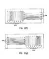
- FIG. 1 ( b )another exemplary structure according to an embodiment of the invention is shown.
- N+ substrate 110two buried conductive elements, line 112 and line 114 .
- Insulative material 116surrounds each line, and also separates lines 112 and 114 from active semiconductor layer 118 .
- deep trench capacitor 120cuts through active layer 118 , insulative material 116 , and within substrate 110 between lines 112 and 114 .
- the deep trench capacitor trenchis filled with P+ silicon, and is surrounded by dielectric material 117 .
- An alternative embodiment to that of FIG. 1 ( b )might have an additional level of buried elements, where the elements are located either in front of and/or behind the plane of the trench capacitor.
- FIG. 1 ( c )still another exemplary structure according to an embodiment of the invention is shown.
- N+ substrate 122two buried conductive layers, layer 124 and 126 .
- Each layerincludes a series of conductive lines.
- Layer 124is oriented in an x plane (parallel to the view shown in FIG. 1 ( c )), and layer 126 is oriented in a y plane (perpendicular to the view shown in FIG. 1 ( c )).
- Insulative material 128surrounds conductive layers 124 and 126 .
- Active semiconductor layer 130lies above the layer formed by insulative material 128 .
- Conductive connection 132is formed prior to the buried wiring, as those of ordinary skill within the art can appreciate. Conductive connection 132 thus provides an external connection to layer 124 ; connection 132 cuts through substrate 122 at the back (bottom) of the structure of FIG. 1 ( c ). Connection 132 may then allow the die of which the structure is a part to be attached electrically to another structure of another die, as described in U.S. Pat. Nos. 5,270,261 and 5,202,754, which are hereby incorporated by reference.
- Connection 132is desirably formed by first etching a hole within substrate 122 , and then oxidizing the surface to provide for insulative material 128 around the hole. A conductive plug may then be deposited to form connection 132 . A metal, such as tungsten or a tungsten alloy, may be the material utilized to form the connection. The invention is not so particularly limited, however.
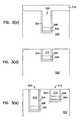
- FIGS. 2 ( a )- 2 ( e )Another exemplary structure according to an embodiment of the invention is shown by reference to FIGS. 2 ( a )- 2 ( e ).
- layer 204 and 206within N+ substrate 200 are two buried conductive layers, layer 204 and 206 , each having a plurality of lines. Each layer is oriented in both the x and y planes; that is, each has a plurality of lines oriented in both the x and y planes.
- Insulative material 208surrounds conductive layers 204 and 206 .
- Active semiconductor layer 210lies above the layer formed by insulative material 208 .
- FIG. 2 ( a )the parts of each layer 204 and 206 oriented in the x plane, parallel to the view shown in FIG. 2 ( a ), are accessible from the top of the structure. That is, a conductive connection to each of these parts of layers 204 and 206
- a first mask pattern used to produce the trenches for (first, lower) layer 206 of the structureis shown.
- Lines 212correspond to the lines of conductive layer 206 that are oriented in the y plane
- lines 214correspond to the lines of conductive layer 206 that are oriented in the x plane.
- FIG. 2 ( c )a second mask pattern used to produce the trenches for (second, higher) layer 204 of the structure is shown.
- Lines 216correspond to the lines of conductive layer 204 that are oriented in the y plane
- lines 218correspond to the lines of conductive layer 204 that are oriented in the x plane.
- FIG. 2 ( d )shows a portion of the silicon island structure that may be used as the seed points for the epitaxial growth of the N+ substrate level
- FIG. 2 ( e )shows a schematic layout of possible contacts to the buried wiring lines (both within layer 204 and layer 206 ).
- the structure of FIGS. 2 ( a )- 2 ( e )thus is a three dimensional semiconductor structure, having two levels of buried wiring lines; each level of buried wiring lines includes lines oriented in the x and the y planes. Such buried wiring lines may render it unnecessary to use external wiring for connections of the structure.
- trench 302within silicon substrate 300 , trench 302 , of the desired width and depth is cut.
- Trench 302has a bottom, and at least two sidewalls.
- Substrate 300is part of a wafer having a front side (top) and a back side (bottom).
- oxidationis performed to produce oxide layer 304 of sufficient thickness to provide electrical insulation for the subsequently formed wire.
- Oxide layer 304is present on the bottom and the walls of trench 302 .
- Seed layer 306is then deposited, desirably using a line of sight deposition process such as collimated sputtering.
- seed layer 306is titanium, although the invention itself is not so limited to this material.
- the seed materialmay be an element selected from groups IVB, VB, or VIB, of the periodic table, for example.
- the seed layer and the oxide on the top surface of the waferis removed, desirably by chemical mechanical polishing (CMP), or another selective removal process.
- CMPchemical mechanical polishing
- the conductive material to be used to form the buried wiring levelis then deposited within the trench, such as tungsten 308 , substantially at the bottom of the trench (i.e., over the seed layer). This is desirably accomplished by a selective metal deposition process, such as plating or chemical vapor deposition.
- Insulative material 310is then deposited to sufficiently fill the trench.
- Material 310may be oxide (silicon dioxide), or any other suitable insulator.
- the top wafer surfaceis again polished by CMP or another suitable process to expose substrate 300 , but not far enough to expose tungsten 308 .
- the exposed substrate 300may then be used as seed points for epitaxial silicon growth. It is noted that the width of tungsten 308 within trench 302 is less than the photo image that was used to etch trench 302 ; thus, it is possible to produce line widths that are less than the minimum photo-definable image.
- FIGS. 3 ( a ) through 3 ( e )may be repeated to produce another level of buried wiring.
- two buried conductorsare present: a deeper conductor at the bottom of trench 302 , and a shallower conductor at the bottom of trench 312 . Greater-depth conductors are formed first, and then lesser-depth conductors are formed. Utilizing the described process, any number of buried wiring levels may be produced. Furthermore, while as described only one trench for each layer has been formed, those of ordinary skill within the art can appreciate that any number of trenches for each layer may be formed.
- the back side of the wafermay be thinned to expose parts of at least the bottom-most conductive layer.
- the first layermay be connected to the second layer, using ion-implanted nitrogen, as described in the coassigned and copending application entitled “Implanted Conductor and Method of Making,” filed Mar. 14, 1997, Ser. No. 08/818,230, or using a conventional fill strategy as known within the art.
- FIG. 1 ( a ) and FIG. 1 ( c )except for the tungsten connection of FIG. 1 ( c ), a process to form such a connection having already been described
- a process to form such a connectionhaving already been described
- N+ wafer0.3 micron width trenches 1.2 microns deep are etched in the silicon to form the spaces for the first (deepest) level of wiring.
- 850 angstrom of thermal oxideare then grown, thus reducing the trench width to 0.225 micron.
- 500 angstroms of CVD oxidemay be deposited.
- the use of a CVD layeris particularly advantageous when several layers of buried wiring are to be used.
- the first wiring levelis constructed.
- a second wiring levelis constructed by first etching 0.3 trenches 0.6 micron deep in the silicon and the oxide where the trench crosses the oxide-covered tungsten of the first wiring level. 850 angstrom silicon oxide is deposited, and 75 angstrom of titanium is deposited. The titanium and oxide on the wafer surface is removed via chemical mechanical polishing. If connections are desired between the two levels of conductors, they can be made through the insulator separating the layers (or the conducting layer and an active device) using ion-implanted nickel, as described in the coassigned and copending application entitled “Implanted Conductor and Method of Making,” filed Mar. 14, 1997, Ser. No. 08/818,230, or using a conventional fill strategy as known within the art.
- tungstenis selectively deposited over the titanium, and chemical mechanical polishing or another suitable technique is used to remove any tungsten inadvertently deposited on the wafer surface.
- 5200 angstrom of oxideis deposited via chemical vapor deposition to fill the trenches and cap the conductors.
- FIG. 1 ( b )A specific process that can be used to form the structure of FIG. 1 ( b ) is now described.
- 0.3 micron width trenches, 0.6 microns deepare etched to form the spaces for the buried level of wiring.
- 850 angstrom of thermal oxideis grown.
- 75 angstrom of titaniumis deposited using collimated sputtering, to provide a seed layer for the conductive material.
- Chemical mechanical polishing, or another suitable techniqueis used to remove titanium and oxide from the wafer surface.
- 0.4 micron of tungstenis selectively deposited at the bottom of the trench, using low temperature hydrogen reduction of tungsten fluoride, where the titanium serves as the seed layer.
- 1075 angstrom of oxideis deposited, and chemical mechanical polishing is used to remove the oxide from the wafer surface.
- the resulting open windows to the N+ siliconare used as nucleation points to grow a P ⁇ silicon epitaxial layer.
- an appropriate photomaskis used to define the areas of P ⁇ /N+ contact, and the deep trench capacitor is etched.
- a desired oxygen-nitrogen-oxygen (ONO) structure, or other dielectric,is grown to provide the capacitor dielectric.
- the capacitor trenchis then filled with P+ polysilicon, and chemical mechanical polishing is used to expose the P ⁇ silicon surface. Conventional processing may then be used to form devices and memory cells within the active layer.
- FIGS. 2 ( a )- 2 ( e )are described.
- 0.3 micron width trenches, 1.2 microns deepare etched to form the spaces for the first (deepest) level of wiring.
- 850 angstrom of thermal oxideis grown, and 75 angstrom of titanium is deposited using collimated sputtering.
- Chemical mechanical polishingis used to remove titanium and oxide from the wafer surface.
- 0.4 micron of tungstenis selectively deposited over the titanium at the bottom of the trench using low temperature hydrogen reduction of tungsten fluoride, the titanium serving as the seed layer. 1450 angstrom of oxide is deposited, and chemical mechanical polishing is used to remove the oxide from the wafer surface.
- 0.3 micron width troughs, 0.6 microns deep,are etched in the silicon and the oxide in the pattern of the upper (second) level of metal.
- 850 angstrom of thermal oxideis CVD deposited and 75 angstrom of titanium is deposited. Titanium and oxide from the wafer surface is removed via chemical mechanical polishing. If connections are desired between the two levels of conductors, they can be made through the insulator separating the layers (or the conducting layer and an active device) using ion-implanted nickel, as described in the coassigned and copending application entitled “Implanted Conductor and Method of Making,” filed Mar. 14, 1997, Ser. No. 08/818,230, or using a conventional fill strategy as known within the art.
- tungsten0.4 microns are selectively deposited over the titanium. If necessary, any tungsten inadvertently deposited on the wafer surface is removed using chemical mechanical polishing or other suitable techniques. 5200 angstrom of oxide is deposited via chemical vapor deposition, and chemical mechanical polishing is used to remove the oxide sufficiently to expose the N+ silicon surface.
- P ⁇ siliconis grown epitaxially. If contacts from the buried wiring levels to structures on or above the P ⁇ epitaxial surface are desired, windows are etched in the epitaxial layer using a mask (such as that which has been shown in FIG. 2 ( d )). An oxide layer equal in thickness to the P ⁇ silicon layer is then deposited, and the surface of the wafer is polished (via chemical mechanical polishing) to expose the P ⁇ silicon; contact is then made to the wiring levels using ion-implanted nickel as described in the coassigned and copending application entitled “Implanted Conductor and Method of Making,” filed Mar. 14, 1997, Ser. No. 08/818,230, or using a conventional fill strategy as known within the art.
- the order of the processes describedmay be modified without affecting materially the final structure produced.
- the oxidecould be removed from the wafer surface prior to titanium deposition, with the titanium on the surface being removed in a subsequent polishing process.
- the seed layer usedcould be other materials besides titanium, such as zirconium.
- the material used for the wiring structurewas described as tungsten, other metals and alloys thereof are suitable. Desirably, a material of sufficiently low resistance to provide a good electrical conductor is used. Sufficient electromigration resistance to enable the required current to be carried without failure during the devices' expected lifetime is desirable.
- the diffusion rate of the element or elements used as conductors through the oxide or other insulatorshould desirably be low enough so that the amount diffusing through the insulating film and into the silicon is insufficient to degrade the properties of the device or devices formed in the various silicon layers.
- the melting point of the metal or alloy usedshould desirably be sufficiently high to prevent its melting or other unwanted metallurgical changes during further processing of the silicon.
- aluminum and aluminum alloys that have been used in traditional wiring applicationsmay have melting points that are low enough to cause concern; however, future changes in processing technology that may lower the temperature requirements of device operation may mute this concern.
- copperwhich has a high diffusion rate in silicon dioxide and is a junction “poison,” as known within the art, is another metal which at the time of filing of this patent application may not be able to be considered for use unless a suitable barrier layer surrounds it.
- the requirements for the buried wiring levelsmay be fulfilled with more or less ease by a number of materials, including the non-radioactive elements of groups IVB, VB, VIB, VIIB, and VIIIB of the periodic table. Of these elements, those in groups VB, VIB and VIIIB may be most desirable because of their lower resistance.
- a material such as tungstenmay be desired because of its reasonably low resistance and because its deposition is relatively well understood by those of ordinary skill within the art.
- selective chemical vapor depositionhas been specifically referenced to deposit the conductive material after the seed layer has been deposited, the invention is not so limited to such deposition.
- electroless platingmay be substituted for selective chemical vapor deposition.
- an alternative materialsuch as polyimide may also be used.
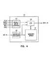
- memory device 10includes memory array 12 , control circuit 14 , input/output buffers 16 , and address decoder 18 .
- Memory array 12includes a plurality of memory cells organized into rows and columns. The memory cells are accessed in response to an address signal provided on the address lines A 0 . . . AN running to address decoder 18 , which includes both row and column decoder circuitry.
- Input/output buffers 16are provided for bi-directional communication via the data communications lines DQ 1 . . . DQN running out of buffers 16 .
- Control circuit 14regulates the memory device operations in response to controls signals including, but not limited to, a Clock (CLK), a Row Access Strobe (RAS*), a Column Access Strobe (CAS*), a Write Enable (WE*), and a Clock Enable (CKE).
- CLKClock
- RAS*Row Access Strobe
- CAS*Column Access Strobe
- WE*Write Enable
- CKEClock Enable
- the present inventionis not limited to any particular type of memory device or repair memory device.
- the devicesare dynamic random-access-memories (DRAMs), including those available from Micron Technology, Inc., of Boise, Id.
- DRAMsdynamic random-access-memories
- the devicesare static random-access-memories (SRAMs), flash memories, synchronous dynamic random-access-memories (SDRAMs), extended-data-out random-access-memories (EDO RAMs), and burst-extended-data-out random-access-memories (BEDO RAMs), as those skilled in the art will appreciate.
- Buried conductorshave been described. The utilization of such conductors provides for internal wiring levels within semiconductor structures and devices, making external wiring levels unnecessary. Thus, three-dimensional structures, such as stacked-chip arrays, may be constructed without resorting to such external wiring levels. This renders these structures faster, and more densely integrated, than would otherwise be possible. Those of ordinary skill within the art can, however, appreciate that other advantages may and can be provided by the invention.
Landscapes
- Engineering & Computer Science (AREA)
- Physics & Mathematics (AREA)
- Condensed Matter Physics & Semiconductors (AREA)
- General Physics & Mathematics (AREA)
- Computer Hardware Design (AREA)
- Microelectronics & Electronic Packaging (AREA)
- Power Engineering (AREA)
- Manufacturing & Machinery (AREA)
- Internal Circuitry In Semiconductor Integrated Circuit Devices (AREA)
Abstract
Description
Claims (34)
Priority Applications (1)
| Application Number | Priority Date | Filing Date | Title |
|---|---|---|---|
| US09/930,521US6946389B2 (en) | 1998-04-29 | 2001-08-15 | Method of forming buried conductors |
Applications Claiming Priority (2)
| Application Number | Priority Date | Filing Date | Title |
|---|---|---|---|
| US09/069,326US6696746B1 (en) | 1998-04-29 | 1998-04-29 | Buried conductors |
| US09/930,521US6946389B2 (en) | 1998-04-29 | 2001-08-15 | Method of forming buried conductors |
Related Parent Applications (1)
| Application Number | Title | Priority Date | Filing Date |
|---|---|---|---|
| US09/069,326DivisionUS6696746B1 (en) | 1998-04-29 | 1998-04-29 | Buried conductors |
Publications (2)
| Publication Number | Publication Date |
|---|---|
| US20020009874A1 US20020009874A1 (en) | 2002-01-24 |
| US6946389B2true US6946389B2 (en) | 2005-09-20 |
Family
ID=22088234
Family Applications (4)
| Application Number | Title | Priority Date | Filing Date |
|---|---|---|---|
| US09/069,326Expired - LifetimeUS6696746B1 (en) | 1998-04-29 | 1998-04-29 | Buried conductors |
| US09/930,521Expired - Fee RelatedUS6946389B2 (en) | 1998-04-29 | 2001-08-15 | Method of forming buried conductors |
| US10/705,185AbandonedUS20040159950A1 (en) | 1998-04-29 | 2003-11-11 | Buried conductors |
| US11/235,041AbandonedUS20060033181A1 (en) | 1998-04-29 | 2005-09-26 | Buried conductors |
Family Applications Before (1)
| Application Number | Title | Priority Date | Filing Date |
|---|---|---|---|
| US09/069,326Expired - LifetimeUS6696746B1 (en) | 1998-04-29 | 1998-04-29 | Buried conductors |
Family Applications After (2)
| Application Number | Title | Priority Date | Filing Date |
|---|---|---|---|
| US10/705,185AbandonedUS20040159950A1 (en) | 1998-04-29 | 2003-11-11 | Buried conductors |
| US11/235,041AbandonedUS20060033181A1 (en) | 1998-04-29 | 2005-09-26 | Buried conductors |
Country Status (1)
| Country | Link |
|---|---|
| US (4) | US6696746B1 (en) |
Cited By (10)
| Publication number | Priority date | Publication date | Assignee | Title |
|---|---|---|---|---|
| US20040219738A1 (en)* | 2000-08-22 | 2004-11-04 | Dinesh Chopra | Method of providing a structure using self-aligned features |
| US20090090950A1 (en)* | 2007-10-05 | 2009-04-09 | Micron Technology, Inc. | Semiconductor devices |
| US7557032B2 (en) | 2005-09-01 | 2009-07-07 | Micron Technology, Inc. | Silicided recessed silicon |
| US20090283854A1 (en)* | 2008-05-19 | 2009-11-19 | Levy Max G | Design Structure and Method for Buried Inductors for Ultra-High Resistivity Wafers for SOI/RF SIGE Applications |
| US7935999B2 (en) | 2005-09-01 | 2011-05-03 | Micron Technology, Inc. | Memory device |
| US7939409B2 (en) | 2005-09-01 | 2011-05-10 | Micron Technology, Inc. | Peripheral gate stacks and recessed array gates |
| US8222105B2 (en) | 2005-08-31 | 2012-07-17 | Micron Technology, Inc. | Methods of fabricating a memory device |
| US8232173B2 (en) | 2010-11-01 | 2012-07-31 | International Business Machines Corporation | Structure and design structure for high-Q value inductor and method of manufacturing the same |
| US9245892B2 (en) | 2014-02-20 | 2016-01-26 | International Business Machines Corporation | Semiconductor structure having buried conductive elements |
| US10515801B2 (en) | 2007-06-04 | 2019-12-24 | Micron Technology, Inc. | Pitch multiplication using self-assembling materials |
Families Citing this family (35)
| Publication number | Priority date | Publication date | Assignee | Title |
|---|---|---|---|---|
| US5977579A (en)* | 1998-12-03 | 1999-11-02 | Micron Technology, Inc. | Trench dram cell with vertical device and buried word lines |
| US6579738B2 (en)* | 2000-12-15 | 2003-06-17 | Micron Technology, Inc. | Method of alignment for buried structures formed by surface transformation of empty spaces in solid state materials |
| US7071043B2 (en) | 2002-08-15 | 2006-07-04 | Micron Technology, Inc. | Methods of forming a field effect transistor having source/drain material over insulative material |
| US6844591B1 (en) | 2003-09-17 | 2005-01-18 | Micron Technology, Inc. | Method of forming DRAM access transistors |
| US7158399B2 (en)* | 2003-10-17 | 2007-01-02 | Micron Technology, Inc. | Digital data apparatuses and digital data operational methods |
| US7262089B2 (en)* | 2004-03-11 | 2007-08-28 | Micron Technology, Inc. | Methods of forming semiconductor structures |
| US7518182B2 (en)* | 2004-07-20 | 2009-04-14 | Micron Technology, Inc. | DRAM layout with vertical FETs and method of formation |
| US7547945B2 (en)* | 2004-09-01 | 2009-06-16 | Micron Technology, Inc. | Transistor devices, transistor structures and semiconductor constructions |
| US7244659B2 (en)* | 2005-03-10 | 2007-07-17 | Micron Technology, Inc. | Integrated circuits and methods of forming a field effect transistor |
| US7384849B2 (en)* | 2005-03-25 | 2008-06-10 | Micron Technology, Inc. | Methods of forming recessed access devices associated with semiconductor constructions |
| US7371627B1 (en)* | 2005-05-13 | 2008-05-13 | Micron Technology, Inc. | Memory array with ultra-thin etched pillar surround gate access transistors and buried data/bit lines |
| US7120046B1 (en)* | 2005-05-13 | 2006-10-10 | Micron Technology, Inc. | Memory array with surrounding gate access transistors and capacitors with global and staggered local bit lines |
| US7888721B2 (en)* | 2005-07-06 | 2011-02-15 | Micron Technology, Inc. | Surround gate access transistors with grown ultra-thin bodies |
| US7282401B2 (en) | 2005-07-08 | 2007-10-16 | Micron Technology, Inc. | Method and apparatus for a self-aligned recessed access device (RAD) transistor gate |
| US7768051B2 (en)* | 2005-07-25 | 2010-08-03 | Micron Technology, Inc. | DRAM including a vertical surround gate transistor |
| US7867851B2 (en)* | 2005-08-30 | 2011-01-11 | Micron Technology, Inc. | Methods of forming field effect transistors on substrates |
| US7867845B2 (en)* | 2005-09-01 | 2011-01-11 | Micron Technology, Inc. | Transistor gate forming methods and transistor structures |
| US7700441B2 (en)* | 2006-02-02 | 2010-04-20 | Micron Technology, Inc. | Methods of forming field effect transistors, methods of forming field effect transistor gates, methods of forming integrated circuitry comprising a transistor gate array and circuitry peripheral to the gate array, and methods of forming integrated circuitry comprising a transistor gate array including first gates and second grounded isolation gates |
| US8501561B2 (en) | 2006-03-07 | 2013-08-06 | Infineon Technologies Ag | Method for producing a semiconductor component arrangement comprising a trench transistor |
| DE102007010884B4 (en)* | 2006-03-07 | 2010-10-07 | Infineon Technologies Ag | Method for producing a semiconductor device arrangement with a trench transistor and semiconductor device arrangement with a trench transistor |
| US8779506B2 (en)* | 2006-03-07 | 2014-07-15 | Infineon Technologies Ag | Semiconductor component arrangement comprising a trench transistor |
| DE102007063728B4 (en)* | 2006-03-07 | 2018-12-13 | Infineon Technologies Ag | Semiconductor device arrangement with a trench transistor |
| US8008144B2 (en) | 2006-05-11 | 2011-08-30 | Micron Technology, Inc. | Dual work function recessed access device and methods of forming |
| US20070262395A1 (en)* | 2006-05-11 | 2007-11-15 | Gibbons Jasper S | Memory cell access devices and methods of making the same |
| US8860174B2 (en)* | 2006-05-11 | 2014-10-14 | Micron Technology, Inc. | Recessed antifuse structures and methods of making the same |
| US8997170B2 (en) | 2006-12-29 | 2015-03-31 | Shared Spectrum Company | Method and device for policy-based control of radio |
| US7602001B2 (en) | 2006-07-17 | 2009-10-13 | Micron Technology, Inc. | Capacitorless one transistor DRAM cell, integrated circuitry comprising an array of capacitorless one transistor DRAM cells, and method of forming lines of capacitorless one transistor DRAM cells |
| US7772632B2 (en)* | 2006-08-21 | 2010-08-10 | Micron Technology, Inc. | Memory arrays and methods of fabricating memory arrays |
| US7589995B2 (en)* | 2006-09-07 | 2009-09-15 | Micron Technology, Inc. | One-transistor memory cell with bias gate |
| US7696057B2 (en)* | 2007-01-02 | 2010-04-13 | International Business Machines Corporation | Method for co-alignment of mixed optical and electron beam lithographic fabrication levels |
| US7927938B2 (en)* | 2007-11-19 | 2011-04-19 | Micron Technology, Inc. | Fin-JFET |
| US7824986B2 (en) | 2008-11-05 | 2010-11-02 | Micron Technology, Inc. | Methods of forming a plurality of transistor gates, and methods of forming a plurality of transistor gates having at least two different work functions |
| US8236691B2 (en)* | 2008-12-31 | 2012-08-07 | Micron Technology, Inc. | Method of high aspect ratio plug fill |
| US9401363B2 (en) | 2011-08-23 | 2016-07-26 | Micron Technology, Inc. | Vertical transistor devices, memory arrays, and methods of forming vertical transistor devices |
| CN114823490B (en)* | 2021-01-27 | 2025-08-19 | 中芯国际集成电路制造(北京)有限公司 | Semiconductor structure |
Citations (41)
| Publication number | Priority date | Publication date | Assignee | Title |
|---|---|---|---|---|
| US3932226A (en) | 1974-12-06 | 1976-01-13 | Rca Corporation | Method of electrically interconnecting semiconductor elements |
| US4461041A (en) | 1983-01-05 | 1984-07-17 | Zenith Radio Corporation | Integrated RF receiver/waveguide |
| US4503451A (en) | 1982-07-30 | 1985-03-05 | Motorola, Inc. | Low resistance buried power bus for integrated circuits |
| GB2179787A (en) | 1985-08-26 | 1987-03-11 | Intel Corp | Buried interconnect for silicon on insulator structure |
| US4670297A (en) | 1985-06-21 | 1987-06-02 | Raytheon Company | Evaporated thick metal and airbridge interconnects and method of manufacture |
| US4857481A (en) | 1989-03-14 | 1989-08-15 | Motorola, Inc. | Method of fabricating airbridge metal interconnects |
| US4912535A (en) | 1987-08-08 | 1990-03-27 | Mitsubishi Denki Kabushiki Kaisha | Trench type semiconductor memory device having side wall contact |
| US4939567A (en) | 1987-12-21 | 1990-07-03 | Ibm Corporation | Trench interconnect for CMOS diffusion regions |
| US4977439A (en) | 1987-04-03 | 1990-12-11 | Esquivel Agerico L | Buried multilevel interconnect system |
| US5158986A (en) | 1991-04-05 | 1992-10-27 | Massachusetts Institute Of Technology | Microcellular thermoplastic foamed with supercritical fluid |
| US5202754A (en) | 1991-09-13 | 1993-04-13 | International Business Machines Corporation | Three-dimensional multichip packages and methods of fabrication |
| US5227658A (en) | 1991-10-23 | 1993-07-13 | International Business Machines Corporation | Buried air dielectric isolation of silicon islands |
| US5232866A (en) | 1991-10-23 | 1993-08-03 | International Business Machines Corporation | Isolated films using an air dielectric |
| US5268315A (en) | 1992-09-04 | 1993-12-07 | Tektronix, Inc. | Implant-free heterojunction bioplar transistor integrated circuit process |
| US5270261A (en) | 1991-09-13 | 1993-12-14 | International Business Machines Corporation | Three dimensional multichip package methods of fabrication |
| US5308440A (en) | 1991-09-05 | 1994-05-03 | Matsushita Electric Industrial Co., Ltd. | Method of making semiconductor device with air-bridge interconnection |
| US5349743A (en) | 1991-05-02 | 1994-09-27 | At&T Bell Laboratories | Method of making a multilayer monolithic magnet component |
| US5382832A (en) | 1992-11-06 | 1995-01-17 | International Business Machines Corporation | Semiconductor device and wafer structure having a planar buried interconnect by wafer bonding |
| US5396093A (en) | 1994-02-14 | 1995-03-07 | Industrial Technology Research Institute | Vertical DRAM cross point memory cell and fabrication method |
| US5410169A (en)* | 1990-02-26 | 1995-04-25 | Kabushiki Kaisha Toshiba | Dynamic random access memory having bit lines buried in semiconductor substrate |
| US5436173A (en) | 1993-01-04 | 1995-07-25 | Texas Instruments Incorporated | Method for forming a semiconductor on insulator device |
| US5438009A (en) | 1993-04-02 | 1995-08-01 | United Microelectronics Corporation | Method of fabrication of MOSFET device with buried bit line |
| US5497017A (en) | 1995-01-26 | 1996-03-05 | Micron Technology, Inc. | Dynamic random access memory array having a cross-point layout, tungsten digit lines buried in the substrate, and vertical access transistors |
| US5504357A (en) | 1991-09-26 | 1996-04-02 | Hyundai Electronics Industries, Co., Ltd. | Dynamic random access memory having a vertical transistor |
| US5539227A (en) | 1993-11-24 | 1996-07-23 | Mitsubishi Denki Kabushiki Kaisha | Multi-layer wiring |
| US5593921A (en) | 1991-09-23 | 1997-01-14 | Sgs-Thomson Microelectronics, Inc. | Method of forming vias |
| US5646067A (en)* | 1995-06-05 | 1997-07-08 | Harris Corporation | Method of bonding wafers having vias including conductive material |
| US5705425A (en) | 1992-05-28 | 1998-01-06 | Fujitsu Limited | Process for manufacturing semiconductor devices separated by an air-bridge |
| US5734676A (en) | 1996-05-24 | 1998-03-31 | International Business Machines Corporation | Apparatus, method and article of manufacture for carrier frequency compensation in a FM radio receiver |
| US5747867A (en) | 1995-01-09 | 1998-05-05 | Siemens Aktiengesellschaft | Integrated circuit structure with interconnect formed along walls of silicon island |
| US5760456A (en) | 1995-12-21 | 1998-06-02 | Grzegorek; Andrew Z. | Integrated circuit compatible planar inductors with increased Q |
| US5798544A (en) | 1994-04-22 | 1998-08-25 | Nec Corporation | Semiconductor memory device having trench isolation regions and bit lines formed thereover |
| US5874770A (en) | 1996-10-10 | 1999-02-23 | General Electric Company | Flexible interconnect film including resistor and capacitor layers |
| US5892707A (en) | 1997-04-25 | 1999-04-06 | Micron Technology, Inc. | Memory array having a digit line buried in an isolation region and method for forming same |
| US5891513A (en)* | 1996-01-16 | 1999-04-06 | Cornell Research Foundation | Electroless CU deposition on a barrier layer by CU contact displacement for ULSI applications |
| US5892425A (en) | 1997-04-10 | 1999-04-06 | Virginia Tech Intellectual Properties, Inc. | Interwound center-tapped spiral inductor |
| US5930668A (en) | 1991-12-31 | 1999-07-27 | Intel Corporation | Process of fabricating embedded ground plane and shielding structures using sidewall insulators in high frequency circuits having vias |
| US5930596A (en) | 1994-03-29 | 1999-07-27 | Siemens Aktiengesellschaft | Semiconductor component for vertical integration and manufacturing method |
| US6025261A (en) | 1998-04-29 | 2000-02-15 | Micron Technology, Inc. | Method for making high-Q inductive elements |
| US6037258A (en)* | 1999-05-07 | 2000-03-14 | Taiwan Semiconductor Manufacturing Company | Method of forming a smooth copper seed layer for a copper damascene structure |
| US6081988A (en) | 1998-04-30 | 2000-07-04 | Lockheed Martin Corp. | Fabrication of a circuit module with a coaxial transmission line |
Family Cites Families (7)
| Publication number | Priority date | Publication date | Assignee | Title |
|---|---|---|---|---|
| DE69133311T2 (en) | 1990-10-15 | 2004-06-24 | Aptix Corp., San Jose | Connection substrate with integrated circuit for programmable connection and sample analysis |
| US5969422A (en) | 1997-05-15 | 1999-10-19 | Advanced Micro Devices, Inc. | Plated copper interconnect structure |
| JPH1197645A (en) | 1997-09-19 | 1999-04-09 | Nec Corp | Semiconductor storage device |
| US6181163B1 (en) | 1999-01-21 | 2001-01-30 | Vantis Corporation | FPGA integrated circuit having embedded SRAM memory blocks and interconnect channel for broadcasting address and control signals |
| JP2002026008A (en) | 2000-07-11 | 2002-01-25 | Nec Corp | Method of forming multilayer interconnect structure and wafer in which multilayer interconnect structure is formed |
| US6271087B1 (en) | 2000-10-10 | 2001-08-07 | Advanced Micro Devices, Inc. | Method for forming self-aligned contacts and local interconnects using self-aligned local interconnects |
| DE10323905A1 (en)* | 2003-05-26 | 2005-01-05 | Infineon Technologies Ag | Method of producing ultrathin homogeneous metal layers |
- 1998
- 1998-04-29USUS09/069,326patent/US6696746B1/ennot_activeExpired - Lifetime
- 2001
- 2001-08-15USUS09/930,521patent/US6946389B2/ennot_activeExpired - Fee Related
- 2003
- 2003-11-11USUS10/705,185patent/US20040159950A1/ennot_activeAbandoned
- 2005
- 2005-09-26USUS11/235,041patent/US20060033181A1/ennot_activeAbandoned
Patent Citations (45)
| Publication number | Priority date | Publication date | Assignee | Title |
|---|---|---|---|---|
| US3932226A (en) | 1974-12-06 | 1976-01-13 | Rca Corporation | Method of electrically interconnecting semiconductor elements |
| US4503451A (en) | 1982-07-30 | 1985-03-05 | Motorola, Inc. | Low resistance buried power bus for integrated circuits |
| US4461041A (en) | 1983-01-05 | 1984-07-17 | Zenith Radio Corporation | Integrated RF receiver/waveguide |
| US4670297A (en) | 1985-06-21 | 1987-06-02 | Raytheon Company | Evaporated thick metal and airbridge interconnects and method of manufacture |
| GB2179787A (en) | 1985-08-26 | 1987-03-11 | Intel Corp | Buried interconnect for silicon on insulator structure |
| US4977439A (en) | 1987-04-03 | 1990-12-11 | Esquivel Agerico L | Buried multilevel interconnect system |
| US4912535A (en) | 1987-08-08 | 1990-03-27 | Mitsubishi Denki Kabushiki Kaisha | Trench type semiconductor memory device having side wall contact |
| US4939567A (en) | 1987-12-21 | 1990-07-03 | Ibm Corporation | Trench interconnect for CMOS diffusion regions |
| US4857481A (en) | 1989-03-14 | 1989-08-15 | Motorola, Inc. | Method of fabricating airbridge metal interconnects |
| US5410169A (en)* | 1990-02-26 | 1995-04-25 | Kabushiki Kaisha Toshiba | Dynamic random access memory having bit lines buried in semiconductor substrate |
| US5158986A (en) | 1991-04-05 | 1992-10-27 | Massachusetts Institute Of Technology | Microcellular thermoplastic foamed with supercritical fluid |
| US5334356A (en) | 1991-04-05 | 1994-08-02 | Massachusetts Institute Of Technology | Supermicrocellular foamed materials |
| US5349743A (en) | 1991-05-02 | 1994-09-27 | At&T Bell Laboratories | Method of making a multilayer monolithic magnet component |
| US5308440A (en) | 1991-09-05 | 1994-05-03 | Matsushita Electric Industrial Co., Ltd. | Method of making semiconductor device with air-bridge interconnection |
| US5202754A (en) | 1991-09-13 | 1993-04-13 | International Business Machines Corporation | Three-dimensional multichip packages and methods of fabrication |
| US5270261A (en) | 1991-09-13 | 1993-12-14 | International Business Machines Corporation | Three dimensional multichip package methods of fabrication |
| US5593921A (en) | 1991-09-23 | 1997-01-14 | Sgs-Thomson Microelectronics, Inc. | Method of forming vias |
| US5504357A (en) | 1991-09-26 | 1996-04-02 | Hyundai Electronics Industries, Co., Ltd. | Dynamic random access memory having a vertical transistor |
| US5232866A (en) | 1991-10-23 | 1993-08-03 | International Business Machines Corporation | Isolated films using an air dielectric |
| US5227658A (en) | 1991-10-23 | 1993-07-13 | International Business Machines Corporation | Buried air dielectric isolation of silicon islands |
| US5930668A (en) | 1991-12-31 | 1999-07-27 | Intel Corporation | Process of fabricating embedded ground plane and shielding structures using sidewall insulators in high frequency circuits having vias |
| US5705425A (en) | 1992-05-28 | 1998-01-06 | Fujitsu Limited | Process for manufacturing semiconductor devices separated by an air-bridge |
| US5268315A (en) | 1992-09-04 | 1993-12-07 | Tektronix, Inc. | Implant-free heterojunction bioplar transistor integrated circuit process |
| US5382832A (en) | 1992-11-06 | 1995-01-17 | International Business Machines Corporation | Semiconductor device and wafer structure having a planar buried interconnect by wafer bonding |
| US5436173A (en) | 1993-01-04 | 1995-07-25 | Texas Instruments Incorporated | Method for forming a semiconductor on insulator device |
| US5438009A (en) | 1993-04-02 | 1995-08-01 | United Microelectronics Corporation | Method of fabrication of MOSFET device with buried bit line |
| US5539227A (en) | 1993-11-24 | 1996-07-23 | Mitsubishi Denki Kabushiki Kaisha | Multi-layer wiring |
| US5396093A (en) | 1994-02-14 | 1995-03-07 | Industrial Technology Research Institute | Vertical DRAM cross point memory cell and fabrication method |
| US5930596A (en) | 1994-03-29 | 1999-07-27 | Siemens Aktiengesellschaft | Semiconductor component for vertical integration and manufacturing method |
| US5798544A (en) | 1994-04-22 | 1998-08-25 | Nec Corporation | Semiconductor memory device having trench isolation regions and bit lines formed thereover |
| US5747867A (en) | 1995-01-09 | 1998-05-05 | Siemens Aktiengesellschaft | Integrated circuit structure with interconnect formed along walls of silicon island |
| US5497017A (en) | 1995-01-26 | 1996-03-05 | Micron Technology, Inc. | Dynamic random access memory array having a cross-point layout, tungsten digit lines buried in the substrate, and vertical access transistors |
| US5646067A (en)* | 1995-06-05 | 1997-07-08 | Harris Corporation | Method of bonding wafers having vias including conductive material |
| US5760456A (en) | 1995-12-21 | 1998-06-02 | Grzegorek; Andrew Z. | Integrated circuit compatible planar inductors with increased Q |
| US5891513A (en)* | 1996-01-16 | 1999-04-06 | Cornell Research Foundation | Electroless CU deposition on a barrier layer by CU contact displacement for ULSI applications |
| US5734676A (en) | 1996-05-24 | 1998-03-31 | International Business Machines Corporation | Apparatus, method and article of manufacture for carrier frequency compensation in a FM radio receiver |
| US5874770A (en) | 1996-10-10 | 1999-02-23 | General Electric Company | Flexible interconnect film including resistor and capacitor layers |
| US5892425A (en) | 1997-04-10 | 1999-04-06 | Virginia Tech Intellectual Properties, Inc. | Interwound center-tapped spiral inductor |
| US5892707A (en) | 1997-04-25 | 1999-04-06 | Micron Technology, Inc. | Memory array having a digit line buried in an isolation region and method for forming same |
| US6025261A (en) | 1998-04-29 | 2000-02-15 | Micron Technology, Inc. | Method for making high-Q inductive elements |
| US6239684B1 (en) | 1998-04-29 | 2001-05-29 | Micron Technology, Inc. | High-Q inductive elements |
| US6376895B2 (en) | 1998-04-29 | 2002-04-23 | Micron Technology, Inc. | High-Q inductive elements |
| US6377156B2 (en) | 1998-04-29 | 2002-04-23 | Micron Technology, Inc. | High-Q inductive elements |
| US6081988A (en) | 1998-04-30 | 2000-07-04 | Lockheed Martin Corp. | Fabrication of a circuit module with a coaxial transmission line |
| US6037258A (en)* | 1999-05-07 | 2000-03-14 | Taiwan Semiconductor Manufacturing Company | Method of forming a smooth copper seed layer for a copper damascene structure |
Non-Patent Citations (7)
| Title |
|---|
| Abidi, "Large Self-Suspended Inductors on Silicon and Their Use in 2-mu m CMOS RF Amplifier", IEEE Electron Device Letters, vol. 17, No. 9, 246-48, (1993). |
| Burghartz, et al., "Integrated RF and Microwave Components in BiCMOS Technology", IEEE Trans. Electron Devices, vol. 43, No. 9, 1559-70, (1996). |
| Burghartz, et al., "Multi-level Spiral Inductors Using VLSI Interconnect Technology", IEEE Electron Device Letters. vol. 17, No. 9, 428-30, (1996). |
| Jin, C., et al., "Porous Xerogel Films as Ultra-low Permittivity Dielectrics for ULSI Interconnect Applications", Conference Proceedings ULSI XII-1997 Materials Research Society, pp. 463-469, (1997). |
| Meyer, et al., "Si IC-Compatible Inductors and LC Passive Filters", IEEE Journal of Solid State Circuits, vol. 25, No. 4, 1028-31, (1990). |
| Miller, R.D., et al., "Low Dielectric Constant Polyimides and Polyimide Nonofoams", Seventh Meeting of the DuPont Symposium on Polymides in Microelectronics, pp. 443-473, (Sep. 1996). |
| Ting, C.H., "Methods and Needs for Low K Material Research", Materials Research Society Symposium Proceedings, vol. 381, Low-Dielectric Constant Materials-Synthesis and Applications in Microelectronics, Lu, T.M., et al., (eds.), San Francisco, CA, 3-17, (Apr. 17-19, 1995). |
Cited By (24)
| Publication number | Priority date | Publication date | Assignee | Title |
|---|---|---|---|---|
| US20040219738A1 (en)* | 2000-08-22 | 2004-11-04 | Dinesh Chopra | Method of providing a structure using self-aligned features |
| US20060154483A1 (en)* | 2000-08-22 | 2006-07-13 | Micron Technology, Inc. | Method of providing a structure using self-aligned features |
| US7109112B2 (en) | 2000-08-22 | 2006-09-19 | Micron Technology, Inc. | Method of providing a structure using self-aligned features |
| US8481385B2 (en) | 2005-08-31 | 2013-07-09 | Micron Technology, Inc. | Methods of fabricating a memory device |
| US8222105B2 (en) | 2005-08-31 | 2012-07-17 | Micron Technology, Inc. | Methods of fabricating a memory device |
| US8546215B2 (en) | 2005-08-31 | 2013-10-01 | Micron Technology, Inc. | Methods of fabricating a memory device |
| US7935999B2 (en) | 2005-09-01 | 2011-05-03 | Micron Technology, Inc. | Memory device |
| US9076888B2 (en) | 2005-09-01 | 2015-07-07 | Micron Technology, Inc. | Silicided recessed silicon |
| US8252646B2 (en) | 2005-09-01 | 2012-08-28 | Micron Technology, Inc. | Peripheral gate stacks and recessed array gates |
| US7939409B2 (en) | 2005-09-01 | 2011-05-10 | Micron Technology, Inc. | Peripheral gate stacks and recessed array gates |
| US7977236B2 (en) | 2005-09-01 | 2011-07-12 | Micron Technology, Inc. | Method of forming a transistor gate of a recessed access device, method of forming a recessed transistor gate and a non-recessed transistor gate, and method of fabricating an integrated circuit |
| US7557032B2 (en) | 2005-09-01 | 2009-07-07 | Micron Technology, Inc. | Silicided recessed silicon |
| US10515801B2 (en) | 2007-06-04 | 2019-12-24 | Micron Technology, Inc. | Pitch multiplication using self-assembling materials |
| US7875529B2 (en) | 2007-10-05 | 2011-01-25 | Micron Technology, Inc. | Semiconductor devices |
| US20090090950A1 (en)* | 2007-10-05 | 2009-04-09 | Micron Technology, Inc. | Semiconductor devices |
| US7842580B2 (en) | 2008-05-19 | 2010-11-30 | International Business Machines Corporation | Structure and method for buried inductors for ultra-high resistivity wafers for SOI/RF SiGe applications |
| US8487379B2 (en) | 2008-05-19 | 2013-07-16 | International Business Machines Corporation | Structure and method for buried inductors for ultra-high resistivity wafers for SOI/RF SiGe applications |
| US8188570B2 (en) | 2008-05-19 | 2012-05-29 | International Business Machines Corporation | Structure and method for buried inductors for ultra-high resistivity wafers for SOI/RF SiGe applications |
| US20100327398A1 (en)* | 2008-05-19 | 2010-12-30 | International Business Machines Corporation | Design structure and method for buried inductors for ultra-high resistivity wafers for soi/rf sige applications |
| US20090283854A1 (en)* | 2008-05-19 | 2009-11-19 | Levy Max G | Design Structure and Method for Buried Inductors for Ultra-High Resistivity Wafers for SOI/RF SIGE Applications |
| US8232173B2 (en) | 2010-11-01 | 2012-07-31 | International Business Machines Corporation | Structure and design structure for high-Q value inductor and method of manufacturing the same |
| US8645898B2 (en) | 2010-11-01 | 2014-02-04 | International Business Machines Corporation | Structure and design structure for high-Q value inductor and method of manufacturing the same |
| US9245892B2 (en) | 2014-02-20 | 2016-01-26 | International Business Machines Corporation | Semiconductor structure having buried conductive elements |
| US9263454B2 (en) | 2014-02-20 | 2016-02-16 | International Business Machines Corporation | Semiconductor structure having buried conductive elements |
Also Published As
| Publication number | Publication date |
|---|---|
| US6696746B1 (en) | 2004-02-24 |
| US20020009874A1 (en) | 2002-01-24 |
| US20040159950A1 (en) | 2004-08-19 |
| US20060033181A1 (en) | 2006-02-16 |
Similar Documents
| Publication | Publication Date | Title |
|---|---|---|
| US6946389B2 (en) | Method of forming buried conductors | |
| US4970564A (en) | Semiconductor memory device having stacked capacitor cells | |
| US5204286A (en) | Method of making self-aligned contacts and vertical interconnects to integrated circuits | |
| US4874719A (en) | Method for manufacturing an electrical connection between conductor levels | |
| US5155059A (en) | Method of manufacturing dynamic RAM | |
| US4833519A (en) | Semiconductor device with a wiring layer having good step coverage for contact holes | |
| US8492813B2 (en) | Semiconductor device and semiconductor device manufacturing method | |
| US5025741A (en) | Method of making semiconductor integrated circuit device with polysilicon contacts | |
| JP2655859B2 (en) | Semiconductor storage device | |
| JPH05198738A (en) | Multichip-package and manufacture thereof | |
| JPH08241931A (en) | Three-dimensional SRAM trench structure and manufacturing method | |
| US5688709A (en) | Method for forming composite trench-fin capacitors for DRAMS | |
| US5276343A (en) | Semiconductor memory device having a bit line constituted by a semiconductor layer | |
| EP0013508A1 (en) | Semiconductor device and a method of producing the same | |
| EP0453998A1 (en) | Semiconductor memory device having a bit line constituted by a semiconductor layer | |
| JP2002289703A (en) | Semiconductor memory and its manufacturing method | |
| JPH031837B2 (en) | ||
| US4975754A (en) | Trench dual-gate MOSFET | |
| JP4918959B2 (en) | DRAM manufactured on silicon-on-insulator (SOI) substrate having two-level digit line, DRAM array, and manufacturing method thereof | |
| JPS5853512B2 (en) | Method for manufacturing semiconductor memory device | |
| JPH03256358A (en) | Semiconductor storage device and its manufacturing method | |
| US5107322A (en) | Wiring or conductor interconnect for a semiconductor device or the like | |
| US7161246B2 (en) | Interconnect alloys and methods and apparatus using same | |
| US6040215A (en) | Method of manufacturing semiconductor device including memory cell having transistor | |
| JP3180760B2 (en) | Method for manufacturing semiconductor device |
Legal Events
| Date | Code | Title | Description |
|---|---|---|---|
| FEPP | Fee payment procedure | Free format text:PAYOR NUMBER ASSIGNED (ORIGINAL EVENT CODE: ASPN); ENTITY STATUS OF PATENT OWNER: LARGE ENTITY | |
| CC | Certificate of correction | ||
| CC | Certificate of correction | ||
| FPAY | Fee payment | Year of fee payment:4 | |
| FPAY | Fee payment | Year of fee payment:8 | |
| AS | Assignment | Owner name:U.S. BANK NATIONAL ASSOCIATION, AS COLLATERAL AGENT, CALIFORNIA Free format text:SECURITY INTEREST;ASSIGNOR:MICRON TECHNOLOGY, INC.;REEL/FRAME:038669/0001 Effective date:20160426 Owner name:U.S. BANK NATIONAL ASSOCIATION, AS COLLATERAL AGEN Free format text:SECURITY INTEREST;ASSIGNOR:MICRON TECHNOLOGY, INC.;REEL/FRAME:038669/0001 Effective date:20160426 | |
| AS | Assignment | Owner name:MORGAN STANLEY SENIOR FUNDING, INC., AS COLLATERAL AGENT, MARYLAND Free format text:PATENT SECURITY AGREEMENT;ASSIGNOR:MICRON TECHNOLOGY, INC.;REEL/FRAME:038954/0001 Effective date:20160426 Owner name:MORGAN STANLEY SENIOR FUNDING, INC., AS COLLATERAL Free format text:PATENT SECURITY AGREEMENT;ASSIGNOR:MICRON TECHNOLOGY, INC.;REEL/FRAME:038954/0001 Effective date:20160426 | |
| REMI | Maintenance fee reminder mailed | ||
| AS | Assignment | Owner name:U.S. BANK NATIONAL ASSOCIATION, AS COLLATERAL AGENT, CALIFORNIA Free format text:CORRECTIVE ASSIGNMENT TO CORRECT THE REPLACE ERRONEOUSLY FILED PATENT #7358718 WITH THE CORRECT PATENT #7358178 PREVIOUSLY RECORDED ON REEL 038669 FRAME 0001. ASSIGNOR(S) HEREBY CONFIRMS THE SECURITY INTEREST;ASSIGNOR:MICRON TECHNOLOGY, INC.;REEL/FRAME:043079/0001 Effective date:20160426 Owner name:U.S. BANK NATIONAL ASSOCIATION, AS COLLATERAL AGEN Free format text:CORRECTIVE ASSIGNMENT TO CORRECT THE REPLACE ERRONEOUSLY FILED PATENT #7358718 WITH THE CORRECT PATENT #7358178 PREVIOUSLY RECORDED ON REEL 038669 FRAME 0001. ASSIGNOR(S) HEREBY CONFIRMS THE SECURITY INTEREST;ASSIGNOR:MICRON TECHNOLOGY, INC.;REEL/FRAME:043079/0001 Effective date:20160426 | |
| LAPS | Lapse for failure to pay maintenance fees | Free format text:PATENT EXPIRED FOR FAILURE TO PAY MAINTENANCE FEES (ORIGINAL EVENT CODE: EXP.) | |
| STCH | Information on status: patent discontinuation | Free format text:PATENT EXPIRED DUE TO NONPAYMENT OF MAINTENANCE FEES UNDER 37 CFR 1.362 | |
| FP | Lapsed due to failure to pay maintenance fee | Effective date:20170920 | |
| AS | Assignment | Owner name:MICRON TECHNOLOGY, INC., IDAHO Free format text:RELEASE BY SECURED PARTY;ASSIGNOR:U.S. BANK NATIONAL ASSOCIATION, AS COLLATERAL AGENT;REEL/FRAME:047243/0001 Effective date:20180629 | |
| AS | Assignment | Owner name:MICRON TECHNOLOGY, INC., IDAHO Free format text:RELEASE BY SECURED PARTY;ASSIGNOR:MORGAN STANLEY SENIOR FUNDING, INC., AS COLLATERAL AGENT;REEL/FRAME:050937/0001 Effective date:20190731 |