US6946053B2 - Plasma reactor - Google Patents
Plasma reactorDownload PDFInfo
- Publication number
- US6946053B2 US6946053B2US10/288,047US28804702AUS6946053B2US 6946053 B2US6946053 B2US 6946053B2US 28804702 AUS28804702 AUS 28804702AUS 6946053 B2US6946053 B2US 6946053B2
- Authority
- US
- United States
- Prior art keywords
- wafer
- chamber
- plasma
- etch
- reactor
- Prior art date
- Legal status (The legal status is an assumption and is not a legal conclusion. Google has not performed a legal analysis and makes no representation as to the accuracy of the status listed.)
- Expired - Fee Related
Links
- 230000008878couplingEffects0.000claimsabstractdescription20
- 238000010168coupling processMethods0.000claimsabstractdescription20
- 238000005859coupling reactionMethods0.000claimsabstractdescription20
- VYPSYNLAJGMNEJ-UHFFFAOYSA-Nsilicon dioxideInorganic materialsO=[Si]=OVYPSYNLAJGMNEJ-UHFFFAOYSA-N0.000claimsabstractdescription20
- 238000005530etchingMethods0.000claimsabstractdescription12
- 229910052710siliconInorganic materials0.000claimsabstractdescription9
- 239000010703siliconSubstances0.000claimsabstractdescription9
- 239000010453quartzSubstances0.000claimsabstractdescription8
- 238000000034methodMethods0.000claimsdescription13
- 230000008569processEffects0.000claimsdescription12
- 230000005684electric fieldEffects0.000claimsdescription9
- BSYNRYMUTXBXSQ-UHFFFAOYSA-NAspirinChemical compoundCC(=O)OC1=CC=CC=C1C(O)=OBSYNRYMUTXBXSQ-UHFFFAOYSA-N0.000claimsdescription6
- 238000009826distributionMethods0.000claimsdescription2
- 239000000758substrateSubstances0.000claims7
- 230000002093peripheral effectEffects0.000claims4
- XUIMIQQOPSSXEZ-UHFFFAOYSA-NSiliconChemical compound[Si]XUIMIQQOPSSXEZ-UHFFFAOYSA-N0.000claims3
- 235000012239silicon dioxideNutrition0.000abstractdescription12
- 239000000377silicon dioxideSubstances0.000abstractdescription6
- 239000003989dielectric materialSubstances0.000abstractdescription4
- 230000004048modificationEffects0.000abstractdescription3
- 238000012986modificationMethods0.000abstractdescription3
- 235000012431wafersNutrition0.000description65
- 210000002381plasmaAnatomy0.000description61
- 150000002500ionsChemical class0.000description23
- 239000007789gasSubstances0.000description19
- 241000894007speciesSpecies0.000description11
- 239000000463materialSubstances0.000description9
- 238000006243chemical reactionMethods0.000description5
- 229910021420polycrystalline siliconInorganic materials0.000description5
- 239000003574free electronSubstances0.000description4
- 230000007246mechanismEffects0.000description4
- 238000004519manufacturing processMethods0.000description3
- 230000007935neutral effectEffects0.000description3
- 230000015572biosynthetic processEffects0.000description2
- 239000006227byproductSubstances0.000description2
- 230000006872improvementEffects0.000description2
- 238000002955isolationMethods0.000description2
- 238000001020plasma etchingMethods0.000description2
- 239000000047productSubstances0.000description2
- 230000001105regulatory effectEffects0.000description2
- 239000004065semiconductorSubstances0.000description2
- 239000000126substanceSubstances0.000description2
- XLYOFNOQVPJJNP-UHFFFAOYSA-NwaterChemical compoundOXLYOFNOQVPJJNP-UHFFFAOYSA-N0.000description2
- JBRZTFJDHDCESZ-UHFFFAOYSA-NAsGaChemical compound[As]#[Ga]JBRZTFJDHDCESZ-UHFFFAOYSA-N0.000description1
- YCKRFDGAMUMZLT-UHFFFAOYSA-NFluorine atomChemical compound[F]YCKRFDGAMUMZLT-UHFFFAOYSA-N0.000description1
- 229910001218Gallium arsenideInorganic materials0.000description1
- 230000001133accelerationEffects0.000description1
- 238000009825accumulationMethods0.000description1
- 230000002411adverseEffects0.000description1
- 238000004774atomic orbitalMethods0.000description1
- 230000015556catabolic processEffects0.000description1
- 238000003486chemical etchingMethods0.000description1
- 239000007795chemical reaction productSubstances0.000description1
- 238000004891communicationMethods0.000description1
- 238000001816coolingMethods0.000description1
- 230000007423decreaseEffects0.000description1
- 239000008367deionised waterSubstances0.000description1
- 229910021641deionized waterInorganic materials0.000description1
- 238000000151depositionMethods0.000description1
- 230000008021depositionEffects0.000description1
- 238000009792diffusion processMethods0.000description1
- 230000005284excitationEffects0.000description1
- 239000012467final productSubstances0.000description1
- 229910052731fluorineInorganic materials0.000description1
- 239000011737fluorineSubstances0.000description1
- 238000010849ion bombardmentMethods0.000description1
- 238000005468ion implantationMethods0.000description1
- 229910021421monocrystalline siliconInorganic materials0.000description1
- 230000003647oxidationEffects0.000description1
- 238000007254oxidation reactionMethods0.000description1
- 229920002120photoresistant polymerPolymers0.000description1
- 125000006850spacer groupChemical group0.000description1
Images


Classifications
- H—ELECTRICITY
- H01—ELECTRIC ELEMENTS
- H01J—ELECTRIC DISCHARGE TUBES OR DISCHARGE LAMPS
- H01J37/00—Discharge tubes with provision for introducing objects or material to be exposed to the discharge, e.g. for the purpose of examination or processing thereof
- H01J37/32—Gas-filled discharge tubes
- H01J37/32009—Arrangements for generation of plasma specially adapted for examination or treatment of objects, e.g. plasma sources
- H01J37/32082—Radio frequency generated discharge
- H—ELECTRICITY
- H01—ELECTRIC ELEMENTS
- H01J—ELECTRIC DISCHARGE TUBES OR DISCHARGE LAMPS
- H01J37/00—Discharge tubes with provision for introducing objects or material to be exposed to the discharge, e.g. for the purpose of examination or processing thereof
- H01J37/32—Gas-filled discharge tubes
- H01J37/32431—Constructional details of the reactor
- H01J37/32623—Mechanical discharge control means
- H01J37/32642—Focus rings
- Y—GENERAL TAGGING OF NEW TECHNOLOGICAL DEVELOPMENTS; GENERAL TAGGING OF CROSS-SECTIONAL TECHNOLOGIES SPANNING OVER SEVERAL SECTIONS OF THE IPC; TECHNICAL SUBJECTS COVERED BY FORMER USPC CROSS-REFERENCE ART COLLECTIONS [XRACs] AND DIGESTS
- Y10—TECHNICAL SUBJECTS COVERED BY FORMER USPC
- Y10S—TECHNICAL SUBJECTS COVERED BY FORMER USPC CROSS-REFERENCE ART COLLECTIONS [XRACs] AND DIGESTS
- Y10S156/00—Adhesive bonding and miscellaneous chemical manufacture
- Y10S156/915—Differential etching apparatus including focus ring surrounding a wafer for plasma apparatus
Definitions
- This inventionrelates to ion-assisted plasma etching of semiconductor wafers in remote source plasma reactors with powered wafer chucks. More particularly, it relates to equipment improvements designed to improve etch uniformity over the surface of a wafer.
- Integrated circuitsare typically fabricated on a wafer of semiconductor material such as silicon or gallium arsenide. During the fabrication process, the wafer is subjected to an ordered series of steps, which may include photomasking, material deposition, oxidation, nitridization, ion implantation, diffusion and etching, in order to achieve a final product.
- ion-assisted etchesalso called reactive-ion, plasma or dry etches
- solution etchesalso called wet etches
- Solution etchesare invariably isotropic (omnidirectional) in nature, with the etch rate for a single material being relatively constant in all directions.
- Reactive-ion etcheson the other hand, are largely anisotropic (unidirectional) in nature.
- Reactive ion etchesare commonly used to create spacers on substantially vertical sidewalls of other layers, to transfer a mask pattern to an underlying layer with little or no undercutting beneath mask segment edges, and to create contact vias in insulative layers.
- a plasma etch system(often referred to as a reactor) is primarily a vacuum chamber in which a glow discharge is utilized to produce a plasma consisting of chemically reactive species (atoms, radicals, and ions) from a relatively inert molecular gas.
- the gasis selected so as to generate species which react either kinetically or chemically with the material to be etched.
- dielectric layerscannot be etched using a direct-current-induced glow discharge due to charge accumulation on the surface of the dielectric which quickly neutralizes the dc-voltage potential, most reactors are designed as radio-frequency diode systems and typically operate at a frequency of 13.56 MHz, a frequency reserved for non-communication use by international agreement.
- plasma etch processes operating between 100 KHz-80 MHzhave been used successfully.
- the first ionization potential of most gas atoms and moleculesis 8 eV and greater. Since plasma electrons have a distribution whose average energy is between 1 to 10 eV, some of these electrons will have sufficient energy to cause ionization of the gas molecules. Collisions of these energized electrons with neutral gas molecules are primarily responsible for the production of the reactive species in a plasma. The reactive species, however, can also react among themselves in the plasma and alter the overall plasma chemistry.
- a plasmais defined to be a partially ionized gas composed of ions, electrons, and a variety of neutral species.
- a radicalis an atom, or collection of atoms, which is electrically neutral, but which also exists in a state of incomplete chemical bonding, making it very reactive.
- Plasma etchesproceed by two basic mechanisms.
- the first, chemical etchingentails the steps of: 1) reactive species are generated in the plasma; 2) these species diffuse to the surface of the material being etched; 3) the species are adsorbed on the surface; 4) a chemical reaction occurs, with the formation of a volatile by-product; 5) the by-product is desorbed from the surface; and 6) the desorbed species diffuse into the bulk of the gas.
- the second, reactive-ion etchinginvolves ionic bombardment of the material to be etched. Since both mechanisms occur simultaneously, the complete plasma etch process would be better aptly identified as an ion-assisted etch process. The greater the chemical mechanism component of the etch, the greater the isotropicity of the etch.
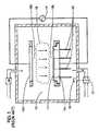
- FIG. 1is a diagrammatic representation of a typical parallel-plate plasma etch reactor.
- a wafer 11is loaded in the reactor chamber 12 and precisely centered on a disk-shaped lower electrode 13 L, thereby becoming electrically integrated therewith.
- a disk-shaped upper electrode 13 Uis positioned, above the wafer (the number 13 * applies to either 13 L or 13 U).
- the flow of molecular gas into the chamber 12is automatically regulated by highly-accurate mass-flow controllers 14 .
- a radio-frequency voltage 15is applied between electrodes 13 L and 13 U. Chamber pressure is monitored and maintained continuously through a feedback loop between a chamber manometer 16 and a downstream throttle valve 17 , which allows reactions products and surplus gas to escape in controlled manner.
- Electrodes Spacing of the electrodesis controlled by a closed-loop, positioning system (not shown).
- a glow dischargewill be established between the electrodes, resulting in a partial ionization of the molecular gas.
- free electronsgain energy from the imposed electric field and lose this energy during collisions with molecules.
- collisionslead to the formation of new species, including metastables, atoms, electrons, free radicals, and ions.
- the electrical discharge between the electrodesconsists of a glowing plasma region 18 centered between lower electrode 13 L and upper electrode 13 U, a lower dark space 19 L between the lower electrode 13 L and plasma region 18 , and an upper dark space region 19 U between the upper electrode 13 U and plasma region 18 .
- Dark space regions 19 *are also known as “sheath” regions. Electrons emitted from the electrodes 13 * are accelerated into the discharge region. By the time the electrons have reached plasma region 18 , they have acquired sufficient kinetic energy to ionize some of the molecular gas molecules and raise the electrons of other molecular gas molecules to less-stable atomic orbitals of increased energy through a mechanism known as electron impact excitation. As each of these excited electrons “relaxes” and falls back to a more stable orbital, a quantum of energy is released in the form of light. This light gives the plasma region its characteristic glow. Free electrons may also collide with species already formed by collisions between free electrons and gas molecules, leading to additional subspecies.
- both electrodesare normally cooled by the circulation of deionized water through the electrodes and an external temperature control unit (not shown). Water cooling prevents elevation of wafer temperature to levels which would destabilize photoresist.
- Typical plasma reactorsconsist of a single process chamber flanked by two loadlock chambers (one for wafer isolation during loading, the other for isolation during unloading).
- Parallel-plate etch reactorshave fallen into disfavor for certain applications.
- the voltage required to sustain the plasmais far higher that is required to etch polycrystalline silicon or single-crystal silicon.
- the voltageis so high that ions are accelerated to energies sufficient to etch silicon dioxide.
- a new type of plasma reactorhas been developed. In this type of reactor, the plasma is generated in a source chamber remote from the wafer (typically at the very top of the chamber, and the wafer chuck is powered separately from the plasma source generator.
- Such a reactoris generally called a high-density source plasma reactor.
- sources used to create the high-density plasmaare: a Mori source, a helicon source, and an electron cyclotron resonance (ECR) source.
- ECRelectron cyclotron resonance
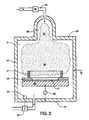
- FIG. 2is a diagrammatic representation of a typical high-density-source plasma reactor.
- the reactorcomprises an etch chamber 21 formed by a cylindrical sidewall 22 , which is grounded, a floor wall 23 , and a ceiling wall 24 .
- a source chamber 25adjoins the etch chamber 21 .
- a disc-shaped wafer chuck 26is concentrically mounted within the lower portion of the etch chamber 21 .
- a wafer 27is precisely centered on the wafer chuck 26 , thereby becoming electrically integrated therewith.
- the wafermay be held in place against the wafer chuck 26 by any one of a variety of known techniques, such as the use of a clamping ring 28 , or an electrostatic chuck (not shown).
- the flow of molecular gaswhich is depicted as being introduced into the source chamber 25 through a primary manifold 29 , is automatically regulated by highly-accurate mass-flow controllers 30 .
- molecular gases and/or atomic gasesmay be introduced at other locations in either the source chamber 25 or the etch chamber 21 .
- a high-density plasma 31is generated within the source chamber 25 by either a Mori source, a helicon source, or an ECR source (not shown).
- a radio-frequency voltage generator 32is coupled between the wafer chuck 26 and ground. Chamber pressure is monitored and maintained continuously through a feedback loop between a chamber manometer 33 and a downstream throttle valve 34 , which allows reactions products and surplus gas to escape in controlled manner.
- the high-density plasmaescapes from the source chamber 25 and migrates toward the etch chamber 21 , its density usually decreases and it usually becomes more spacially uniform.
- the less dense plasma 35 within the etch chamber 21receives additional power from the powered wafer chuck during the etch process.
- Power coupling between the wafer chuck 26 and the cylindrical sidewall 22causes reactive ions to be accelerated through a dark space that is established just above the surface of the wafer 27 , permitting ion-assisted etching of etchable material on the surface of the wafer to occur.
- the amount of power supplied to the wafer chuck 26greatly influences etch rates, etch uniformity, and profile control
- the discussion of ion-assisted etching relative to the parallel-plate etch reactoris also largely applicable in the case of a high-density source plasma reactor.
- cylindrical sidewall 22is normally fitted with a large number of vertical magnetic strips of alternating polarity, thus creating a magnetic field wall on the interior surface of cylindrical sidewall 22 .
- Such an arrangementis known as a “McKenzie bucket” or simply a “confinement bucket”, and was devised as a means to more evenly distribute reactive ions which were generated within the source chamber 25 and which have migrated downward to the etch chamber 21 . This feature is not depicted, as it is not relevant to this invention.
- Nonuniform power coupling between the wafer and the walls of the etch chambercan be the dominant cause of nonuniform etching rates across the surface of the wafer.
- Nonuniform power couplingoccurs because regions near wafer edge are physically closer to the grounded walls of the chamber than are regions closer to the wafer center.
- higher poweris coupled to the walls through a unit area near the edge of the wafer than is coupled by a unit area located nearer the center of the wafer.
- This radially nonuniform coupling of the rf power to the chamber wallsresults in lower etch rates near the center of the wafer than near the edge. It can also adversely affect other process results such as feature profile and/or selectivity.
- This inventionis a hardware modification which permits greater uniformity of etching to be achieved in a high-density-source plasma reactor (i.e., one which uses a remote source to generate a plasma, and which also uses high-frequency bias power on the wafer chuck).
- the inventionaddresses the uniformity problem which arises as the result of nonuniform power coupling between the wafer and the walls of the etch chamber.
- the solution to greatly mitigate the nonuniformity problemis to increase the impedance between the wafer and the chamber walls. This may be accomplished by placing a cylindrical dielectric wall around the wafer. Quartz is a dielectric material that is ideal for the cylindrical wall if silicon is to be etched selectively with respect to silicon dioxide, as quartz it is virtually inert under such conditions. Any dielectric material can be used, including those which are etchable, provided that they do not have a negative impact on the etch process.
- FIG. 1is a diagrammatic representation of a typical parallel-plate plasma etch reactor
- FIG. 2is a diagrammatic representation of a typical remote plasma source etch reactor having a powered wafer chuck
- FIG. 3is a diagrammatic representation of the remote plasma source etch reactor of FIG. 2 , which has been fitted with a cylindrical dielectric wall decoupler;
- FIG. 4Ais a plot of the etch rate for polycrystalline silicon, in ⁇ /min., as a function of location on the wafer for a power setting of 3,000 watts for the source plasma generator and about 95 watts for the wafer chuck power setting for both a standard high-density source plasma reactor and a high-density source plasma reactor which incorporates the invention;
- FIG. 4Bis a plot of the etch rate for polycrystalline silicon, in ⁇ /min., as a function of location on the wafer for a power setting of 3,000 watts for the source plasma generator and about 60 watts for the wafer chuck power setting for both a standard high-density source plasma reactor and a high-density source plasma reactor which incorporates the invention;
- FIG. 4Cis a plot of the etch rate for polycrystalline silicon, in ⁇ /min., as a function of location on the wafer for a power setting of 3,000 watts for the source plasma generator and about 31 watts for the wafer chuck power setting for both a standard high-density source plasma reactor and a high-density source plasma reactor which incorporates the invention.
- the impedance-increasing deviceis a cylindrical dielectric wall 37 that, like the wafer 27 , is precisely centered (ie., concentrically mounted) on the wafer chuck 26 .
- Quartzis a dielectric material that is ideal for the cylindrical wall 35 if silicon is to be etched selectively with respect to silicon dioxide, as quartz it is virtually inert under wafer chuck power settings of 60 watts.
- FIGS. 4A , 4 B, and 4 Cdemonstrate the effectiveness of the invention at a plasma source power setting of 3,000 watts, but at different wafer chuck power settings.
- the circular data pointsrepresent measured data for the standard reactor without the dielectric wall 37
- the square data pointsrepresent measured data for the reactor with the dielectric wall 37 .
- FIG. 4Ais a plot of the etch rate for polycrystalline silicon, in ⁇ /min., as a function of location on a six-inch wafer. Position 3 represents the center of the wafer, and positions 0 and 6 represent the edges of the wafer.
- the wafer chuck power settingswere approximately 95 watts, 60 watts, and 31 watts, respectively. It will be noted that at a wafer chuck power setting of approximately 95 watts, etch uniformity is measurably improved with the dielectric wall 35 installed in the reactor. However, substantial nonuniformity is still present.
Landscapes
- Physics & Mathematics (AREA)
- Engineering & Computer Science (AREA)
- Plasma & Fusion (AREA)
- Chemical & Material Sciences (AREA)
- Analytical Chemistry (AREA)
- Drying Of Semiconductors (AREA)
- Plasma Technology (AREA)
Abstract
Description
This application is a continuation of U.S. patent application Ser. No. 10/132,589 filed Apr. 25, 2002 (issued as U.S. Pat. No. 6,500,300) which is a continuation of Ser. No. 09/922,587 filed Aug. 3, 2001 (issued as U.S. Pat. No. 6,413,358), which is a continuation of Ser. No. 08/823,275 filed Mar. 24, 1997 (issued as U.S. Pat. No. 6,290,806), which is a continuation of Ser. No. 08/524249 filed Sep. 6, 1995 (issued as U.S. Pat. No. 5,904,799), which is a divisional of Ser. No. 08/048,991 filed Apr. 16, 1993 (issued as U.S. Pat. No. 5,662,770). Priority is claimed to these prior applications, and they are all incorporated by reference herein.
This invention relates to ion-assisted plasma etching of semiconductor wafers in remote source plasma reactors with powered wafer chucks. More particularly, it relates to equipment improvements designed to improve etch uniformity over the surface of a wafer.
Integrated circuits are typically fabricated on a wafer of semiconductor material such as silicon or gallium arsenide. During the fabrication process, the wafer is subjected to an ordered series of steps, which may include photomasking, material deposition, oxidation, nitridization, ion implantation, diffusion and etching, in order to achieve a final product.
There are two basic types of etches: ion-assisted etches (also called reactive-ion, plasma or dry etches) and solution etches (also called wet etches). Solution etches are invariably isotropic (omnidirectional) in nature, with the etch rate for a single material being relatively constant in all directions. Reactive-ion etches, on the other hand, are largely anisotropic (unidirectional) in nature. Reactive ion etches are commonly used to create spacers on substantially vertical sidewalls of other layers, to transfer a mask pattern to an underlying layer with little or no undercutting beneath mask segment edges, and to create contact vias in insulative layers.
A plasma etch system (often referred to as a reactor) is primarily a vacuum chamber in which a glow discharge is utilized to produce a plasma consisting of chemically reactive species (atoms, radicals, and ions) from a relatively inert molecular gas. The gas is selected so as to generate species which react either kinetically or chemically with the material to be etched. Because dielectric layers cannot be etched using a direct-current-induced glow discharge due to charge accumulation on the surface of the dielectric which quickly neutralizes the dc-voltage potential, most reactors are designed as radio-frequency diode systems and typically operate at a frequency of 13.56 MHz, a frequency reserved for non-communication use by international agreement. However, plasma etch processes operating between 100 KHz-80 MHz have been used successfully.
The first ionization potential of most gas atoms and molecules is 8 eV and greater. Since plasma electrons have a distribution whose average energy is between 1 to 10 eV, some of these electrons will have sufficient energy to cause ionization of the gas molecules. Collisions of these energized electrons with neutral gas molecules are primarily responsible for the production of the reactive species in a plasma. The reactive species, however, can also react among themselves in the plasma and alter the overall plasma chemistry.
Since plasmas consisting of fluorine-containing gases are extensively used for etching silicon, silicon dioxide, and other materials used in VLSI fabrication, it is instructive to examine the glow-discharge chemistry of CF4. Initially, the only species present are CF4molecules. However, once a glow discharge is established, a portion of the CF4molecules dissociated into other species. A plasma is defined to be a partially ionized gas composed of ions, electrons, and a variety of neutral species. The most abundant ionic specie found in CF4plasmas is CF3+, such ions being formed by the electron-impact reaction: e+CF4=>CF3++F+2e. In addition to CF4molecules, ionic species, and electrons, a large number of radicals are formed. A radical is an atom, or collection of atoms, which is electrically neutral, but which also exists in a state of incomplete chemical bonding, making it very reactive. In CF4plasmas, the most abundant radicals are CF3and F, formed by the reaction: e+CF4=>CF3+F+e. Radicals are generally thought to exist in plasmas in much higher concentrations than ions, because they are generated at a faster rate, and they survive longer than ions in the plasma.
Plasma etches proceed by two basic mechanisms. The first, chemical etching, entails the steps of: 1) reactive species are generated in the plasma; 2) these species diffuse to the surface of the material being etched; 3) the species are adsorbed on the surface; 4) a chemical reaction occurs, with the formation of a volatile by-product; 5) the by-product is desorbed from the surface; and 6) the desorbed species diffuse into the bulk of the gas. The second, reactive-ion etching, involves ionic bombardment of the material to be etched. Since both mechanisms occur simultaneously, the complete plasma etch process would be better aptly identified as an ion-assisted etch process. The greater the chemical mechanism component of the etch, the greater the isotropicity of the etch.
Parallel-plate etch reactors have fallen into disfavor for certain applications. For example, the voltage required to sustain the plasma is far higher that is required to etch polycrystalline silicon or single-crystal silicon. In fact, the voltage is so high that ions are accelerated to energies sufficient to etch silicon dioxide. For this reason, it is very difficult to perform an etch of silicon that stops on a silicon dioxide layer using a parallel-plate reactor. For such applications, a new type of plasma reactor has been developed. In this type of reactor, the plasma is generated in a source chamber remote from the wafer (typically at the very top of the chamber, and the wafer chuck is powered separately from the plasma source generator. Such a reactor is generally called a high-density source plasma reactor. Examples of sources used to create the high-density plasma are: a Mori source, a helicon source, and an electron cyclotron resonance (ECR) source. A description of the operation of such sources is beyond the scope of this disclosure, and not particularly relevant thereto.
Still referring toFIG. 2 , it should be noted that thecylindrical sidewall 22 is normally fitted with a large number of vertical magnetic strips of alternating polarity, thus creating a magnetic field wall on the interior surface ofcylindrical sidewall 22. Such an arrangement is known as a “McKenzie bucket” or simply a “confinement bucket”, and was devised as a means to more evenly distribute reactive ions which were generated within thesource chamber 25 and which have migrated downward to theetch chamber 21. This feature is not depicted, as it is not relevant to this invention.
One of the problems associated with high-density source plasma etch reactors is that etching is not uniform across the surface of the wafer. Nonuniform power coupling between the wafer and the walls of the etch chamber can be the dominant cause of nonuniform etching rates across the surface of the wafer. Nonuniform power coupling occurs because regions near wafer edge are physically closer to the grounded walls of the chamber than are regions closer to the wafer center. Thus, higher power is coupled to the walls through a unit area near the edge of the wafer than is coupled by a unit area located nearer the center of the wafer. This radially nonuniform coupling of the rf power to the chamber walls results in lower etch rates near the center of the wafer than near the edge. It can also adversely affect other process results such as feature profile and/or selectivity.
This invention is a hardware modification which permits greater uniformity of etching to be achieved in a high-density-source plasma reactor (i.e., one which uses a remote source to generate a plasma, and which also uses high-frequency bias power on the wafer chuck). The invention addresses the uniformity problem which arises as the result of nonuniform power coupling between the wafer and the walls of the etch chamber. The solution to greatly mitigate the nonuniformity problem is to increase the impedance between the wafer and the chamber walls. This may be accomplished by placing a cylindrical dielectric wall around the wafer. Quartz is a dielectric material that is ideal for the cylindrical wall if silicon is to be etched selectively with respect to silicon dioxide, as quartz it is virtually inert under such conditions. Any dielectric material can be used, including those which are etchable, provided that they do not have a negative impact on the etch process.
Referring now toFIG. 3 , a conventional high-density-source plasma reactor has been fitted with a device which uniformly increases the impedance between the wafer and the chamber walls. The impedance-increasing device is acylindrical dielectric wall 37 that, like thewafer 27, is precisely centered (ie., concentrically mounted) on the wafer chuck26. Quartz is a dielectric material that is ideal for thecylindrical wall 35 if silicon is to be etched selectively with respect to silicon dioxide, as quartz it is virtually inert under wafer chuck power settings of 60 watts. It is hypothesized that power coupling between the wafer and thechamber wall 22 is uneven because the electrical paths from the wafer surface, through the dark space above the wafer surface, through theplasma 35, and, finally, to thechamber wall 22, are of different lengths, depending on the radial location on the surface of the wafer. The center of the wafer is the farthest from the wall, so one would expect power coupling for the wafer's center region to be less than for the wafer's edge. Actual etch rates do support to this hypothesis. It is assumed that thedielectric wall 37 is successful in improving the uniformity of etch rate because it increase the power coupling path for all portions of thewafer 27. However, the increase in path length is greater for portions of the wafer nearest the edge.
Although only a single embodiment of the invention has been disclosed herein, it will be obvious to those having ordinary skill in the art of ion-assisted etching that changes and modifications may be made thereto without departing from the scope and the spirit of the invention as hereinafter claimed.
Claims (39)
1. A plasma etch reactor, comprising:
a main chamber with a sidewall;
a wafer chuck for receiving a wafer within the main chamber;
a source chamber for delivering plasma to the main chamber;
a dielectric ring surrounding a received wafer on the wafer chuck; and
a voltage source electrically coupled between the wafer chuck and the chamber sidewall.
2. The reactor ofclaim 1 , wherein the dielectric ring reduces coupling between the received wafer and the chamber sidewall thereby increasing the uniformity of an etch across the wafer.
3. The reactor ofclaim 2 , wherein the dielectric ring extends above a plane defined by an upper surface of the received wafer.
4. The reactor ofclaim 3 , wherein the main chamber sidewall is grounded.
5. The reactor ofclaim 3 , wherein the plasma is a high density plasma.
6. The reactor ofclaim 4 , wherein the source chamber comprises a source selected from the group consisting of a Mori source, a helicon source, and an ECR source.
7. A plasma etch reactor, comprising:
a chamber with a sidewall;
a wafer chuck for supporting a wafer within the chamber;
a dielectric ring surrounding a wafer on the wafer chuck;
a first power source for generating a plasma; and
a second power source electrically coupled between the wafer chuck and the sidewall for directing the plasma to etch the wafer.
8. The reactor ofclaim 7 , wherein the dielectric ring reduces coupling between the wafer and the chamber sidewall thereby increasing the uniformity of an etch across the wafer.
9. The reactor ofclaim 8 , wherein the dielectric ring extends above a plane defined by an upper surface of the wafer.
10. The reactor ofclaim 9 , wherein the chamber sidewall is grounded.
11. The reactor ofclaim 10 , wherein the dielectric ring comprises quartz.
12. The reactor ofclaim 11 , wherein the first power source generates a high density plasma.
13. The reactor ofclaim 12 , wherein the first power source is selected from the group consisting of a Mori source, a helicon source, and an ECR source.
14. The reactor ofclaim 7 , wherein the first power source generates the plasma at a source chamber coupled to the chamber.
15. A plasma etch reactor, comprising:
a chamber with a sidewall;
a wafer chuck configured to support a wafer within the chamber;
a first power source for generating a plasma;
a second power source electrically coupled between the wafer chuck and the sidewall to control the etch of the wafer by the plasma; and
dielectric ring means positioned within the chamber for increasing the uniformity of the etch rate across the wafer.
16. The reactor ofclaim 15 , wherein the dielectric ring means reduces coupling between the wafer and the chamber sidewall thereby increasing the uniformity of the etch across the wafer.
17. The reactor ofclaim 16 , wherein the dielectric ring means extends above a plane defined by an upper surface of the wafer.
18. The reactor ofclaim 17 , wherein the first power source generates a high density plasma.
19. The reactor ofclaim 15 , wherein the first power source generates the plasma at a source chamber coupled to the chamber.
20. A plasma etch reactor, comprising:
a chamber with a sidewall;
a wafer chuck for supporting a wafer within the chamber;
a power source electrically coupled between the wafer chuck and the sidewall; and
a dielectric wall surrounding the wafer on the wafer chuck and extending above a plane defined by the upper surface of the wafer, the dielectric wall increasing the uniformity of the power coupling between the upper surface of the wafer and the sidewall.
21. The reactor ofclaim 20 , wherein the dielectric wall increases the uniformity of the power coupling by increasing the impedance between the upper surface of the wafer and the sidewall.
22. The reactor ofclaim 20 , further comprising a plasma generating power source for generating a plasma within the chamber.
23. A plasma etch reactor, comprising:
a chamber with a sidewall;
a wafer chuck within the chamber for supporting a wafer, the wafer comprising a center region and an edge region;
a power source electrically coupled to the wafer chuck and the sidewall; and
a dielectric wall surrounding the wafer and having an upper surface above a plane defined by an upper surface of the wafer, the dielectric wall increasing the power coupling path between all regions of the wafer and the sidewall, whereby the increase in power coupling path is greater for the edge region of the wafer than for the center region of the wafer, thereby increasing the uniformity of an etch process across the wafer.
24. The reactor ofclaim 23 , further comprising a plasma generating power source for generating a plasma within the chamber.
25. A plasma etch reactor, comprising:
a chamber with a sidewall;
a first power source for generating a plasma in a first chamber region;
a second chamber region comprising a wafer chuck for supporting a wafer, the wafer comprising a center region and an edge region;
a second power source electrically coupled between the wafer chuck and the sidewall; and
a dielectric wall surrounding the wafer, the dielectric wall shaped in a manner to increase the power coupling path between all regions of the wafer and the sidewall, whereby the increase in power coupling path is greater for the edge region of the wafer than for the center region of the wafer, thereby increasing the uniformity of an etch process across the wafer.
26. The reactor ofclaim 25 , wherein the first power source generates a high density plasma.
27. A plasma etch reactor, comprising:
walls defining an etch chamber;
a wafer chuck disposed in the etch chamber for supporting a wafer;
a first power source for generating a plasma in a first region of the etch chamber;
a second power source electrically coupled between the wafer chuck and the etch chamber walls for assisting in etching of the wafer, thereby forming electric fields between an upper surface of the wafer and the etch chamber walls; and
a dielectric wall around a periphery of the wafer, the dielectric wall extending above a plane defined by the upper surface of the wafer, thereby affecting an impedance in the electric fields between the upper surface of the wafer and the etch chamber walls.
28. The reactor ofclaim 27 , wherein the first power source generates a high density plasma.
29. The reactor ofclaim 28 , wherein the first power source is selected from the group consisting of a Mori source, a helicon source, and an ECR source.
30. A plasma etch reactor for etching a substrate, comprising:
walls defining an etch chamber;
a wafer chuck disposed within the etch chamber walls, the wafer chuck seating a substrate;
a dielectric wall surrounding the substrate, the dielectric wall extending above a plane defined by an upper surface of the substrate;
a first voltage source for creating a plasma in a first region of the chamber; and
a second voltage source electrically coupled between the wafer chuck and the etch chamber walls to form electric fields between the upper surface of the substrate and the etch chamber walls,
wherein the dielectric wall has a height sufficient to cause portions of the electric fields associated with a peripheral region of the upper surface of the substrate to traverse the dielectric wall, thereby affecting a power density distribution produced by the electrical field across the upper surface of the substrate.
31. A plasma etch reactor, comprising:
an etch chamber with walls;
a plasma source generator for generating plasma in a first region of the etch chamber;
a wafer chuck on which a wafer may be affixed, the wafer chuck being positioned between the etch chamber walls;
a radio-frequency voltage source for generating a potential electrically coupled between the wafer chuck and the etch chamber walls and for applying electrical energy to the wafer chuck such that when a plasma is present in the etch chamber, electrical fields will be established between the wafer and the etch chamber walls; and
a dielectric wall which is installed concentrically with a circumference of the wafer and which extends above an upper surface of the wafer so that the electric fields between the upper surface of the wafer and the etch chamber walls include portions having paths which traverse the dielectric wall.
32. A plasma etch reactor, comprising:
an etch chamber having circumferential walls;
a wafer chuck having a circular upper surface upon which a wafer may be placed, the wafer chuck being positioned with its upper surface in concentric relationship to the circumferential walls;
a first power supply electrically coupled between the wafer chuck and the circumferential walls, the power supply being configured to supply a radio frequency bias to the wafer chuck relative the circumferential walls with a power magnitude insufficient to generate a plasma above the wafer chuck within the etch chamber;
a second power supply for generating a plasma within the etch chamber; and
a cylindrical dielectric wall positioned concentric to and extending above a plane formed by an upper surface of a wafer placed on the wafer chuck, the dielectric wall providing an electro-magnetic impedance between the upper surface of the wafer and the circumferential walls.
33. The reactor ofclaim 32 , wherein the etch chamber walls are grounded.
34. The reactor ofclaim 33 , wherein the dielectric wall comprises quartz.
35. The reactor ofclaim 34 , wherein the second power supply generates a high density plasma.
36. The reactor ofclaim 35 , wherein the second power supply comprises a source selected from the group consisting of a Mori source, a helicon source, and an ECR source.
37. A plasma etch reactor, comprising:
a conductive wafer chuck having an upper surface for supporting a wafer;
an etch chamber having a conductive perimetric wall which surrounds but does not contact the wafer chuck;
a first power supply electrically coupled between the wafer chuck and the perimetric wall, the first power supply being configured to supply a radio frequency bias to the wafer chuck;
a second power supply separate from the first power supply for generating a plasma within the etch chamber; and
a cylindrical dielectric wall interposed between a peripheral upper surface of a wafer affixed to the wafer chuck and the etch chamber wall, the dielectric wall extending upwardly from a plane formed by the peripheral upper surface of the wafer to affect the electro-magnetic characteristics between the upper peripheral surface of the wafer and the etch chamber wall.
38. A plasma etcher for etching silicon, comprising:
a chamber with a sidewall;
a wafer chuck within the chamber for supporting a wafer, the wafer comprising a silicon layer;
a first power source for generating a plasma from a fluorinated gas;
a second power source electrically coupled between the wafer chuck and the sidewall for directing the plasma to etch the silicon layer on the wafer; and
a dielectric wall surrounding a wafer on the wafer chuck, the dielectric wall shaped in a manner to increase the power coupling path between all regions of the wafer and the sidewall, thereby increasing the uniformity of an etch process across the wafer.
39. The plasma etcher ofclaim 38 , wherein the wafer comprises a center region and an edge region, and whereby the dielectric wall is shaped such that the increase in the power coupling path is greater for the edge region of the wafer than for the center region of the wafer.
Priority Applications (2)
| Application Number | Priority Date | Filing Date | Title |
|---|---|---|---|
| US10/288,047US6946053B2 (en) | 1993-04-16 | 2002-11-05 | Plasma reactor |
| US11/101,730US20050173376A1 (en) | 1993-04-16 | 2005-04-08 | Method for etching a wafer in a plasma etch reactor |
Applications Claiming Priority (6)
| Application Number | Priority Date | Filing Date | Title |
|---|---|---|---|
| US08/048,991US5662770A (en) | 1993-04-16 | 1993-04-16 | Method and apparatus for improving etch uniformity in remote source plasma reactors with powered wafer chucks |
| US08/524,249US5904799A (en) | 1993-04-16 | 1995-09-06 | Method and apparatus for improving etch uniformity in remote source plasma reactors with powered wafer chucks |
| US08/823,275US6290806B1 (en) | 1993-04-16 | 1997-03-24 | Plasma reactor |
| US09/922,587US6413358B2 (en) | 1993-04-16 | 2001-08-03 | Method and apparatus for improving etch uniformity in remote source plasma reactors with powered wafer chucks |
| US10/132,589US6500300B2 (en) | 1993-04-16 | 2002-04-25 | Plasma reactor |
| US10/288,047US6946053B2 (en) | 1993-04-16 | 2002-11-05 | Plasma reactor |
Related Parent Applications (1)
| Application Number | Title | Priority Date | Filing Date |
|---|---|---|---|
| US10/132,589ContinuationUS6500300B2 (en) | 1993-04-16 | 2002-04-25 | Plasma reactor |
Related Child Applications (1)
| Application Number | Title | Priority Date | Filing Date |
|---|---|---|---|
| US11/101,730DivisionUS20050173376A1 (en) | 1993-04-16 | 2005-04-08 | Method for etching a wafer in a plasma etch reactor |
Publications (2)
| Publication Number | Publication Date |
|---|---|
| US20030062127A1 US20030062127A1 (en) | 2003-04-03 |
| US6946053B2true US6946053B2 (en) | 2005-09-20 |
Family
ID=21957511
Family Applications (7)
| Application Number | Title | Priority Date | Filing Date |
|---|---|---|---|
| US08/048,991Expired - LifetimeUS5662770A (en) | 1993-04-16 | 1993-04-16 | Method and apparatus for improving etch uniformity in remote source plasma reactors with powered wafer chucks |
| US08/524,249Expired - LifetimeUS5904799A (en) | 1993-04-16 | 1995-09-06 | Method and apparatus for improving etch uniformity in remote source plasma reactors with powered wafer chucks |
| US08/823,275Expired - Fee RelatedUS6290806B1 (en) | 1993-04-16 | 1997-03-24 | Plasma reactor |
| US09/922,587Expired - Fee RelatedUS6413358B2 (en) | 1993-04-16 | 2001-08-03 | Method and apparatus for improving etch uniformity in remote source plasma reactors with powered wafer chucks |
| US10/132,589Expired - Fee RelatedUS6500300B2 (en) | 1993-04-16 | 2002-04-25 | Plasma reactor |
| US10/288,047Expired - Fee RelatedUS6946053B2 (en) | 1993-04-16 | 2002-11-05 | Plasma reactor |
| US11/101,730AbandonedUS20050173376A1 (en) | 1993-04-16 | 2005-04-08 | Method for etching a wafer in a plasma etch reactor |
Family Applications Before (5)
| Application Number | Title | Priority Date | Filing Date |
|---|---|---|---|
| US08/048,991Expired - LifetimeUS5662770A (en) | 1993-04-16 | 1993-04-16 | Method and apparatus for improving etch uniformity in remote source plasma reactors with powered wafer chucks |
| US08/524,249Expired - LifetimeUS5904799A (en) | 1993-04-16 | 1995-09-06 | Method and apparatus for improving etch uniformity in remote source plasma reactors with powered wafer chucks |
| US08/823,275Expired - Fee RelatedUS6290806B1 (en) | 1993-04-16 | 1997-03-24 | Plasma reactor |
| US09/922,587Expired - Fee RelatedUS6413358B2 (en) | 1993-04-16 | 2001-08-03 | Method and apparatus for improving etch uniformity in remote source plasma reactors with powered wafer chucks |
| US10/132,589Expired - Fee RelatedUS6500300B2 (en) | 1993-04-16 | 2002-04-25 | Plasma reactor |
Family Applications After (1)
| Application Number | Title | Priority Date | Filing Date |
|---|---|---|---|
| US11/101,730AbandonedUS20050173376A1 (en) | 1993-04-16 | 2005-04-08 | Method for etching a wafer in a plasma etch reactor |
Country Status (1)
| Country | Link |
|---|---|
| US (7) | US5662770A (en) |
Cited By (8)
| Publication number | Priority date | Publication date | Assignee | Title |
|---|---|---|---|---|
| US20070081294A1 (en)* | 2005-10-11 | 2007-04-12 | Applied Materials, Inc. | Capacitively coupled plasma reactor having very agile wafer temperature control |
| US20070081295A1 (en)* | 2005-10-11 | 2007-04-12 | Applied Materials, Inc. | Capacitively coupled plasma reactor having a cooled/heated wafer support with uniform temperature distribution |
| US20070081296A1 (en)* | 2005-10-11 | 2007-04-12 | Applied Materials, Inc. | Method of operating a capacitively coupled plasma reactor with dual temperature control loops |
| US20070091537A1 (en)* | 2005-10-20 | 2007-04-26 | Applied Materials, Inc. | Method for agile workpiece temperature control in a plasma reactor using a thermal model |
| US20070097580A1 (en)* | 2005-10-11 | 2007-05-03 | Applied Materials, Inc. | Method of cooling a wafer support at a uniform temperature in a capacitively coupled plasma reactor |
| US20110143551A1 (en)* | 2008-04-28 | 2011-06-16 | Christophe Borean | Device and process for chemical vapor phase treatment |
| US20120193580A1 (en)* | 2011-01-27 | 2012-08-02 | Southwest Research Institute | Enhancement Of Syngas Production In Coal Gasification With CO2 Conversion Under Plasma Conditions |
| US8679368B2 (en) | 2010-12-22 | 2014-03-25 | Southwest Research Institute | Synthetic hydrocarbon production by direct reduction of carbonaceous materials with synthesis gas |
Families Citing this family (106)
| Publication number | Priority date | Publication date | Assignee | Title |
|---|---|---|---|---|
| US5662770A (en) | 1993-04-16 | 1997-09-02 | Micron Technology, Inc. | Method and apparatus for improving etch uniformity in remote source plasma reactors with powered wafer chucks |
| US5891350A (en) | 1994-12-15 | 1999-04-06 | Applied Materials, Inc. | Adjusting DC bias voltage in plasma chambers |
| JP3257328B2 (en)* | 1995-03-16 | 2002-02-18 | 株式会社日立製作所 | Plasma processing apparatus and plasma processing method |
| JP3516523B2 (en)* | 1995-05-30 | 2004-04-05 | アネルバ株式会社 | Plasma processing equipment |
| US7294578B1 (en)* | 1995-06-02 | 2007-11-13 | Micron Technology, Inc. | Use of a plasma source to form a layer during the formation of a semiconductor device |
| US5950092A (en)* | 1995-06-02 | 1999-09-07 | Micron Technology, Inc. | Use of a plasma source to form a layer during the formation of a semiconductor device |
| US6716769B1 (en) | 1995-06-02 | 2004-04-06 | Micron Technology, Inc. | Use of a plasma source to form a layer during the formation of a semiconductor device |
| US6267840B1 (en)* | 1996-09-11 | 2001-07-31 | Steven R. Vosen | Low pressure stagnation flow reactor with a flow barrier |
| US6274459B1 (en)* | 1998-02-17 | 2001-08-14 | Silicon Genesis Corporation | Method for non mass selected ion implant profile control |
| US6095085A (en)* | 1998-08-20 | 2000-08-01 | Micron Technology, Inc. | Photo-assisted remote plasma apparatus and method |
| US6069087A (en)* | 1998-08-25 | 2000-05-30 | Micron Technology, Inc. | Highly selective dry etching process |
| US6143079A (en)* | 1998-11-19 | 2000-11-07 | Asm America, Inc. | Compact process chamber for improved process uniformity |
| US6261406B1 (en)* | 1999-01-11 | 2001-07-17 | Lsi Logic Corporation | Confinement device for use in dry etching of substrate surface and method of dry etching a wafer surface |
| US6374831B1 (en)* | 1999-02-04 | 2002-04-23 | Applied Materials, Inc. | Accelerated plasma clean |
| US6335292B1 (en)* | 1999-04-15 | 2002-01-01 | Micron Technology, Inc. | Method of controlling striations and CD loss in contact oxide etch |
| US6344105B1 (en)* | 1999-06-30 | 2002-02-05 | Lam Research Corporation | Techniques for improving etch rate uniformity |
| US6257168B1 (en)* | 1999-06-30 | 2001-07-10 | Lam Research Corporation | Elevated stationary uniformity ring design |
| US6368988B1 (en) | 1999-07-16 | 2002-04-09 | Micron Technology, Inc. | Combined gate cap or digit line and spacer deposition using HDP |
| US6436303B1 (en)* | 1999-07-21 | 2002-08-20 | Applied Materials, Inc. | Film removal employing a remote plasma source |
| JP2001185542A (en)* | 1999-12-27 | 2001-07-06 | Hitachi Ltd | Plasma processing apparatus and plasma processing method using the same |
| KR100767762B1 (en)* | 2000-01-18 | 2007-10-17 | 에이에스엠 저펜 가부시기가이샤 | A CVD semiconductor-processing device provided with a remote plasma source for self cleaning |
| US6478924B1 (en)* | 2000-03-07 | 2002-11-12 | Applied Materials, Inc. | Plasma chamber support having dual electrodes |
| US7141757B2 (en)* | 2000-03-17 | 2006-11-28 | Applied Materials, Inc. | Plasma reactor with overhead RF source power electrode having a resonance that is virtually pressure independent |
| US7220937B2 (en)* | 2000-03-17 | 2007-05-22 | Applied Materials, Inc. | Plasma reactor with overhead RF source power electrode with low loss, low arcing tendency and low contamination |
| US6900596B2 (en)* | 2002-07-09 | 2005-05-31 | Applied Materials, Inc. | Capacitively coupled plasma reactor with uniform radial distribution of plasma |
| US6894245B2 (en)* | 2000-03-17 | 2005-05-17 | Applied Materials, Inc. | Merie plasma reactor with overhead RF electrode tuned to the plasma with arcing suppression |
| US8048806B2 (en) | 2000-03-17 | 2011-11-01 | Applied Materials, Inc. | Methods to avoid unstable plasma states during a process transition |
| US7030335B2 (en)* | 2000-03-17 | 2006-04-18 | Applied Materials, Inc. | Plasma reactor with overhead RF electrode tuned to the plasma with arcing suppression |
| US6528751B1 (en) | 2000-03-17 | 2003-03-04 | Applied Materials, Inc. | Plasma reactor with overhead RF electrode tuned to the plasma |
| US8617351B2 (en) | 2002-07-09 | 2013-12-31 | Applied Materials, Inc. | Plasma reactor with minimal D.C. coils for cusp, solenoid and mirror fields for plasma uniformity and device damage reduction |
| US7196283B2 (en) | 2000-03-17 | 2007-03-27 | Applied Materials, Inc. | Plasma reactor overhead source power electrode with low arcing tendency, cylindrical gas outlets and shaped surface |
| US6853141B2 (en) | 2002-05-22 | 2005-02-08 | Daniel J. Hoffman | Capacitively coupled plasma reactor with magnetic plasma control |
| US6362110B1 (en)* | 2000-03-30 | 2002-03-26 | Lam Research Corporation | Enhanced resist strip in a dielectric etcher using downstream plasma |
| US6475889B1 (en)* | 2000-04-11 | 2002-11-05 | Cree, Inc. | Method of forming vias in silicon carbide and resulting devices and circuits |
| US7125786B2 (en)* | 2000-04-11 | 2006-10-24 | Cree, Inc. | Method of forming vias in silicon carbide and resulting devices and circuits |
| US7892974B2 (en)* | 2000-04-11 | 2011-02-22 | Cree, Inc. | Method of forming vias in silicon carbide and resulting devices and circuits |
| US6489249B1 (en)* | 2000-06-20 | 2002-12-03 | Infineon Technologies Ag | Elimination/reduction of black silicon in DT etch |
| US6930041B2 (en)* | 2000-12-07 | 2005-08-16 | Micron Technology, Inc. | Photo-assisted method for semiconductor fabrication |
| US6576564B2 (en) | 2000-12-07 | 2003-06-10 | Micron Technology, Inc. | Photo-assisted remote plasma apparatus and method |
| US7025856B2 (en)* | 2001-02-02 | 2006-04-11 | The Regents Of The University Of California | Processing materials inside an atmospheric-pressure radiofrequency nonthermal plasma discharge |
| US7159597B2 (en)* | 2001-06-01 | 2007-01-09 | Applied Materials, Inc. | Multistep remote plasma clean process |
| US6868856B2 (en)* | 2001-07-13 | 2005-03-22 | Applied Materials, Inc. | Enhanced remote plasma cleaning |
| US6627465B2 (en)* | 2001-08-30 | 2003-09-30 | Micron Technology, Inc. | System and method for detecting flow in a mass flow controller |
| US6737358B2 (en) | 2002-02-13 | 2004-05-18 | Intel Corporation | Plasma etching uniformity control |
| US6451647B1 (en) | 2002-03-18 | 2002-09-17 | Advanced Micro Devices, Inc. | Integrated plasma etch of gate and gate dielectric and low power plasma post gate etch removal of high-K residual |
| KR100432972B1 (en)* | 2002-03-25 | 2004-05-28 | 어댑티브프라즈마테크놀로지 주식회사 | Plasma etching system, Apparatus combined that, and Apparatus and Method for testing that |
| US6843858B2 (en)* | 2002-04-02 | 2005-01-18 | Applied Materials, Inc. | Method of cleaning a semiconductor processing chamber |
| TWI283899B (en)* | 2002-07-09 | 2007-07-11 | Applied Materials Inc | Capacitively coupled plasma reactor with magnetic plasma control |
| US20040231798A1 (en)* | 2002-09-13 | 2004-11-25 | Applied Materials, Inc. | Gas delivery system for semiconductor processing |
| KR101276694B1 (en)* | 2003-02-14 | 2013-06-19 | 어플라이드 머티어리얼스, 인코포레이티드 | Cleaning of native oxide with hydrogen-containing radicals |
| US7232767B2 (en)* | 2003-04-01 | 2007-06-19 | Mattson Technology, Inc. | Slotted electrostatic shield modification for improved etch and CVD process uniformity |
| US7037376B2 (en)* | 2003-04-11 | 2006-05-02 | Applied Materials Inc. | Backflush chamber clean |
| KR100954895B1 (en)* | 2003-05-14 | 2010-04-27 | 도쿄엘렉트론가부시키가이샤 | Thin Film Removal Device and Thin Film Removal Method |
| US7795153B2 (en) | 2003-05-16 | 2010-09-14 | Applied Materials, Inc. | Method of controlling a chamber based upon predetermined concurrent behavior of selected plasma parameters as a function of selected chamber parameters |
| US7247218B2 (en) | 2003-05-16 | 2007-07-24 | Applied Materials, Inc. | Plasma density, energy and etch rate measurements at bias power input and real time feedback control of plasma source and bias power |
| US7901952B2 (en)* | 2003-05-16 | 2011-03-08 | Applied Materials, Inc. | Plasma reactor control by translating desired values of M plasma parameters to values of N chamber parameters |
| US7452824B2 (en)* | 2003-05-16 | 2008-11-18 | Applied Materials, Inc. | Method of characterizing a chamber based upon concurrent behavior of selected plasma parameters as a function of plural chamber parameters |
| US7470626B2 (en)* | 2003-05-16 | 2008-12-30 | Applied Materials, Inc. | Method of characterizing a chamber based upon concurrent behavior of selected plasma parameters as a function of source power, bias power and chamber pressure |
| US7910013B2 (en) | 2003-05-16 | 2011-03-22 | Applied Materials, Inc. | Method of controlling a chamber based upon predetermined concurrent behavior of selected plasma parameters as a function of source power, bias power and chamber pressure |
| US7075771B2 (en)* | 2003-05-21 | 2006-07-11 | Tokyo Electron Limited | Apparatus and methods for compensating plasma sheath non-uniformities at the substrate in a plasma processing system |
| US7169233B2 (en)* | 2003-11-21 | 2007-01-30 | Asm America, Inc. | Reactor chamber |
| US20050115924A1 (en)* | 2003-12-01 | 2005-06-02 | Justin Sato | Integration function of RF signal to analyze steady state and non-steady state ( initializaion) of plasmas |
| US7431772B2 (en)* | 2004-03-09 | 2008-10-07 | Applied Materials, Inc. | Gas distributor having directed gas flow and cleaning method |
| US20060000802A1 (en)* | 2004-06-30 | 2006-01-05 | Ajay Kumar | Method and apparatus for photomask plasma etching |
| US8349128B2 (en)* | 2004-06-30 | 2013-01-08 | Applied Materials, Inc. | Method and apparatus for stable plasma processing |
| US20060021633A1 (en)* | 2004-07-27 | 2006-02-02 | Applied Materials, Inc. | Closed loop clean gas control |
| US20060162661A1 (en)* | 2005-01-22 | 2006-07-27 | Applied Materials, Inc. | Mixing energized and non-energized gases for silicon nitride deposition |
| US7359177B2 (en)* | 2005-05-10 | 2008-04-15 | Applied Materials, Inc. | Dual bias frequency plasma reactor with feedback control of E.S.C. voltage using wafer voltage measurement at the bias supply output |
| US7713430B2 (en)* | 2006-02-23 | 2010-05-11 | Micron Technology, Inc. | Using positive DC offset of bias RF to neutralize charge build-up of etch features |
| US7943005B2 (en) | 2006-10-30 | 2011-05-17 | Applied Materials, Inc. | Method and apparatus for photomask plasma etching |
| US7909961B2 (en)* | 2006-10-30 | 2011-03-22 | Applied Materials, Inc. | Method and apparatus for photomask plasma etching |
| US8614151B2 (en)* | 2008-01-04 | 2013-12-24 | Micron Technology, Inc. | Method of etching a high aspect ratio contact |
| US8382941B2 (en) | 2008-09-15 | 2013-02-26 | Micron Technology, Inc. | Plasma reactor with adjustable plasma electrodes and associated methods |
| US7967913B2 (en)* | 2008-10-22 | 2011-06-28 | Applied Materials, Inc. | Remote plasma clean process with cycled high and low pressure clean steps |
| GB0823282D0 (en) | 2008-12-20 | 2009-01-28 | Univ Strathclyde | Dose responsive UV indicator |
| US20100270262A1 (en)* | 2009-04-22 | 2010-10-28 | Applied Materials, Inc. | Etching low-k dielectric or removing resist with a filtered ionized gas |
| US11171008B2 (en) | 2011-03-01 | 2021-11-09 | Applied Materials, Inc. | Abatement and strip process chamber in a dual load lock configuration |
| US10453694B2 (en) | 2011-03-01 | 2019-10-22 | Applied Materials, Inc. | Abatement and strip process chamber in a dual loadlock configuration |
| WO2012148568A1 (en) | 2011-03-01 | 2012-11-01 | Applied Materials, Inc. | Method and apparatus for substrate transfer and radical confinement |
| JP6545460B2 (en) | 2012-02-29 | 2019-07-17 | アプライド マテリアルズ インコーポレイテッドApplied Materials,Incorporated | Abatement and stripping process chamber in load lock configuration |
| US9530618B2 (en) | 2012-07-06 | 2016-12-27 | Infineon Technologies Ag | Plasma system, chuck and method of making a semiconductor device |
| CN109166782B (en) | 2013-11-06 | 2020-08-07 | 应用材料公司 | Particle Generation Suppressor by DC Bias Modulation |
| US10510575B2 (en) | 2017-09-20 | 2019-12-17 | Applied Materials, Inc. | Substrate support with multiple embedded electrodes |
| US10555412B2 (en) | 2018-05-10 | 2020-02-04 | Applied Materials, Inc. | Method of controlling ion energy distribution using a pulse generator with a current-return output stage |
| US11476145B2 (en) | 2018-11-20 | 2022-10-18 | Applied Materials, Inc. | Automatic ESC bias compensation when using pulsed DC bias |
| KR102827481B1 (en) | 2019-01-22 | 2025-06-30 | 어플라이드 머티어리얼스, 인코포레이티드 | Feedback loop to control pulse voltage waveform |
| US11848176B2 (en) | 2020-07-31 | 2023-12-19 | Applied Materials, Inc. | Plasma processing using pulsed-voltage and radio-frequency power |
| TWI746222B (en)* | 2020-10-21 | 2021-11-11 | 財團法人工業技術研究院 | Deposition apparatus |
| US11901157B2 (en) | 2020-11-16 | 2024-02-13 | Applied Materials, Inc. | Apparatus and methods for controlling ion energy distribution |
| US11798790B2 (en) | 2020-11-16 | 2023-10-24 | Applied Materials, Inc. | Apparatus and methods for controlling ion energy distribution |
| US11495470B1 (en) | 2021-04-16 | 2022-11-08 | Applied Materials, Inc. | Method of enhancing etching selectivity using a pulsed plasma |
| US11948780B2 (en) | 2021-05-12 | 2024-04-02 | Applied Materials, Inc. | Automatic electrostatic chuck bias compensation during plasma processing |
| US11791138B2 (en) | 2021-05-12 | 2023-10-17 | Applied Materials, Inc. | Automatic electrostatic chuck bias compensation during plasma processing |
| US11967483B2 (en) | 2021-06-02 | 2024-04-23 | Applied Materials, Inc. | Plasma excitation with ion energy control |
| US20220399185A1 (en) | 2021-06-09 | 2022-12-15 | Applied Materials, Inc. | Plasma chamber and chamber component cleaning methods |
| US12394596B2 (en) | 2021-06-09 | 2025-08-19 | Applied Materials, Inc. | Plasma uniformity control in pulsed DC plasma chamber |
| US11810760B2 (en) | 2021-06-16 | 2023-11-07 | Applied Materials, Inc. | Apparatus and method of ion current compensation |
| US11569066B2 (en) | 2021-06-23 | 2023-01-31 | Applied Materials, Inc. | Pulsed voltage source for plasma processing applications |
| US11776788B2 (en) | 2021-06-28 | 2023-10-03 | Applied Materials, Inc. | Pulsed voltage boost for substrate processing |
| US11476090B1 (en) | 2021-08-24 | 2022-10-18 | Applied Materials, Inc. | Voltage pulse time-domain multiplexing |
| US12106938B2 (en) | 2021-09-14 | 2024-10-01 | Applied Materials, Inc. | Distortion current mitigation in a radio frequency plasma processing chamber |
| US11694876B2 (en) | 2021-12-08 | 2023-07-04 | Applied Materials, Inc. | Apparatus and method for delivering a plurality of waveform signals during plasma processing |
| US11972924B2 (en) | 2022-06-08 | 2024-04-30 | Applied Materials, Inc. | Pulsed voltage source for plasma processing applications |
| US12315732B2 (en) | 2022-06-10 | 2025-05-27 | Applied Materials, Inc. | Method and apparatus for etching a semiconductor substrate in a plasma etch chamber |
| US12272524B2 (en) | 2022-09-19 | 2025-04-08 | Applied Materials, Inc. | Wideband variable impedance load for high volume manufacturing qualification and on-site diagnostics |
| US12111341B2 (en) | 2022-10-05 | 2024-10-08 | Applied Materials, Inc. | In-situ electric field detection method and apparatus |
Citations (80)
| Publication number | Priority date | Publication date | Assignee | Title |
|---|---|---|---|---|
| US3669860A (en) | 1970-04-01 | 1972-06-13 | Zenith Radio Corp | Method and apparatus for applying a film to a substrate surface by diode sputtering |
| US3691103A (en) | 1969-03-25 | 1972-09-12 | Magyar Tudomanyos Akademia | Process for the preparation of a non-pyrophoric nickel skeleton catalyst |
| US3730873A (en) | 1970-03-18 | 1973-05-01 | Philips Corp | Cathode sputtering etching device with movable guard ring |
| US3875068A (en) | 1973-02-20 | 1975-04-01 | Tegal Corp | Gaseous plasma reaction apparatus |
| US4165395A (en) | 1977-06-30 | 1979-08-21 | International Business Machines Corporation | Process for forming a high aspect ratio structure by successive exposures with electron beam and actinic radiation |
| US4350578A (en) | 1981-05-11 | 1982-09-21 | International Business Machines Corporation | Cathode for etching |
| US4492620A (en) | 1982-09-10 | 1985-01-08 | Nippon Telegraph & Telephone Public Corporation | Plasma deposition method and apparatus |
| US4521286A (en)* | 1983-03-09 | 1985-06-04 | Unisearch Limited | Hollow cathode sputter etcher |
| US4557797A (en) | 1984-06-01 | 1985-12-10 | Texas Instruments Incorporated | Resist process using anti-reflective coating |
| US4581100A (en)* | 1984-10-29 | 1986-04-08 | International Business Machines Corporation | Mixed excitation plasma etching system |
| JPS6230327A (en) | 1985-03-27 | 1987-02-09 | Hitachi Ltd | Dry etching device |
| US4645218A (en) | 1984-07-31 | 1987-02-24 | Kabushiki Kaisha Tokuda Seisakusho | Electrostatic chuck |
| US4657616A (en)* | 1985-05-17 | 1987-04-14 | Benzing Technologies, Inc. | In-situ CVD chamber cleaner |
| US4741928A (en)* | 1985-12-27 | 1988-05-03 | General Electric Company | Method for selective deposition of tungsten by chemical vapor deposition onto metal and semiconductor surfaces |
| US4745044A (en) | 1985-04-26 | 1988-05-17 | International Business Machines Corporation | Multilayer resists with improved sensitivity and reduced proximity effect |
| US4776918A (en)* | 1986-10-20 | 1988-10-11 | Hitachi, Ltd. | Plasma processing apparatus |
| US4786359A (en) | 1987-06-24 | 1988-11-22 | Tegal Corporation | Xenon enhanced plasma etch |
| US4793975A (en) | 1985-05-20 | 1988-12-27 | Tegal Corporation | Plasma Reactor with removable insert |
| US4828369A (en)* | 1986-05-28 | 1989-05-09 | Minolta Camera Kabushiki Kaisha | Electrochromic device |
| US4842708A (en) | 1982-02-16 | 1989-06-27 | Teijin Limited | Perpendicular magnetic recording medium, method for producing the same, and sputtering device |
| US4895765A (en)* | 1985-09-30 | 1990-01-23 | Union Carbide Corporation | Titanium nitride and zirconium nitride coating compositions, coated articles and methods of manufacture |
| US4929322A (en)* | 1985-09-30 | 1990-05-29 | Union Carbide Corporation | Apparatus and process for arc vapor depositing a coating in an evacuated chamber |
| US4943345A (en)* | 1989-03-23 | 1990-07-24 | Board Of Trustees Operating Michigan State University | Plasma reactor apparatus and method for treating a substrate |
| JPH02246113A (en)* | 1989-03-17 | 1990-10-01 | Matsushita Electric Ind Co Ltd | Dryetching device |
| US4971651A (en)* | 1990-02-05 | 1990-11-20 | Hitachi, Ltd. | Microwave plasma processing method and apparatus |
| US4989541A (en)* | 1989-02-23 | 1991-02-05 | Nobuo Mikoshiba | Thin film forming apparatus |
| US4989544A (en)* | 1989-01-26 | 1991-02-05 | Canon Kabushiki Kaisha | Apparatus for forming functional deposited films by way of hybrid excitation |
| JPH0344028A (en) | 1989-07-11 | 1991-02-25 | Matsushita Electron Corp | Apparatus for plasma etching |
| US4996077A (en) | 1988-10-07 | 1991-02-26 | Texas Instruments Incorporated | Distributed ECR remote plasma processing and apparatus |
| US5006760A (en) | 1987-01-09 | 1991-04-09 | Motorola, Inc. | Capacitive feed for plasma reactor |
| US5019117A (en)* | 1986-12-29 | 1991-05-28 | Sumitomo Metal Industries Ltd. | Plasma apparatus |
| US5087341A (en) | 1984-03-23 | 1992-02-11 | Anelva Corporation | Dry etching apparatus and method |
| US5091208A (en)* | 1990-03-05 | 1992-02-25 | Wayne State University | Novel susceptor for use in chemical vapor deposition apparatus and its method of use |
| US5169676A (en)* | 1991-05-16 | 1992-12-08 | The United States Of America As Represented By The Secretary Of The Navy | Control of crystallite size in diamond film chemical vapor deposition |
| JPH0556939A (en) | 1991-08-30 | 1993-03-09 | Hans Baell | Blood flow measuring device |
| US5213658A (en)* | 1990-10-26 | 1993-05-25 | Mitsubishi Denki Kabushiki Kaisha | Plasma processing method |
| US5246532A (en)* | 1990-10-26 | 1993-09-21 | Mitsubishi Denki Kabushiki Kaisha | Plasma processing apparatus |
| US5252178A (en) | 1992-06-24 | 1993-10-12 | Texas Instruments Incorporated | Multi-zone plasma processing method and apparatus |
| US5255153A (en) | 1990-07-20 | 1993-10-19 | Tokyo Electron Limited | Electrostatic chuck and plasma apparatus equipped therewith |
| US5254171A (en)* | 1991-04-16 | 1993-10-19 | Sony Corporation | Bias ECR plasma CVD apparatus comprising susceptor, clamp, and chamber wall heating and cooling means |
| US5269848A (en)* | 1987-03-20 | 1993-12-14 | Canon Kabushiki Kaisha | Process for preparing a functional thin film by way of the chemical reaction among active species and apparatus therefor |
| JPH0653176A (en) | 1992-07-30 | 1994-02-25 | Matsushita Electron Corp | Dry etcher |
| US5292677A (en) | 1992-09-18 | 1994-03-08 | Micron Technology, Inc. | Reduced mask CMOS process for fabricating stacked capacitor multi-megabit dynamic random access memories utilizing single etch stop layer for contacts |
| US5320982A (en) | 1990-07-02 | 1994-06-14 | Hitachi, Ltd. | Wafer cooling method and apparatus |
| US5338700A (en) | 1993-04-14 | 1994-08-16 | Micron Semiconductor, Inc. | Method of forming a bit line over capacitor array of memory cells |
| JPH06267898A (en) | 1993-03-17 | 1994-09-22 | Tokyo Electron Ltd | Vacuum treatment device |
| JPH06283472A (en) | 1993-03-29 | 1994-10-07 | Tokyo Electron Ltd | Plasma device and plasma processing method |
| JPH06283474A (en) | 1993-03-27 | 1994-10-07 | Tokyo Electron Ltd | Plasma processing device |
| US5362666A (en) | 1992-09-18 | 1994-11-08 | Micron Technology, Inc. | Method of producing a self-aligned contact penetrating cell plate |
| US5376227A (en) | 1992-11-12 | 1994-12-27 | Goldstar Electron Co., Ltd. | Multilevel resist process |
| US5378654A (en) | 1994-05-24 | 1995-01-03 | United Microelectronics Corporation | Self-aligned contact process |
| US5384018A (en) | 1992-05-26 | 1995-01-24 | Balzers Aktiengesellschaft | Process and apparatus for generating and igniting a low-voltage |
| US5407529A (en) | 1992-03-04 | 1995-04-18 | Nec Corporation | Method for manufacturing semiconductor device |
| US5421891A (en)* | 1989-06-13 | 1995-06-06 | Plasma & Materials Technologies, Inc. | High density plasma deposition and etching apparatus |
| US5423918A (en)* | 1993-09-21 | 1995-06-13 | Applied Materials, Inc. | Method for reducing particulate contamination during plasma processing of semiconductor devices |
| US5429070A (en)* | 1989-06-13 | 1995-07-04 | Plasma & Materials Technologies, Inc. | High density plasma deposition and etching apparatus |
| US5494522A (en) | 1993-03-17 | 1996-02-27 | Tokyo Electron Limited | Plasma process system and method |
| US5556500A (en) | 1994-03-03 | 1996-09-17 | Tokyo Electron Limited | Plasma etching apparatus |
| US5567267A (en)* | 1992-11-20 | 1996-10-22 | Tokyo Electron Limited | Method of controlling temperature of susceptor |
| US5597763A (en) | 1993-07-27 | 1997-01-28 | Samsung Electronics Co., Ltd. | Method for manufacturing a semiconductor wiring structure including a self-aligned contact hole |
| US5651855A (en) | 1992-07-28 | 1997-07-29 | Micron Technology, Inc. | Method of making self aligned contacts to silicon substrates during the manufacture of integrated circuits |
| US5660673A (en)* | 1993-08-31 | 1997-08-26 | Nec Corporation | Apparatus for dry etching |
| US5670404A (en) | 1996-06-21 | 1997-09-23 | Industrial Technology Research Institute | Method for making self-aligned bit line contacts on a DRAM circuit having a planarized insulating layer |
| US5753886A (en)* | 1995-02-07 | 1998-05-19 | Seiko Epson Corporation | Plasma treatment apparatus and method |
| US5830624A (en) | 1994-07-14 | 1998-11-03 | Hyundai Electronics Industries Co., Ltd. | Method for forming resist patterns comprising two photoresist layers and an intermediate layer |
| US5897923A (en)* | 1994-09-30 | 1999-04-27 | Anelva Corporation | Plasma treatment device |
| US5904799A (en)* | 1993-04-16 | 1999-05-18 | Micron Technology, Inc. | Method and apparatus for improving etch uniformity in remote source plasma reactors with powered wafer chucks |
| US5933314A (en) | 1997-06-27 | 1999-08-03 | Lam Research Corp. | Method and an apparatus for offsetting plasma bias voltage in bi-polar electro-static chucks |
| US5959325A (en) | 1997-08-21 | 1999-09-28 | International Business Machines Corporation | Method for forming cornered images on a substrate and photomask formed thereby |
| US6022446A (en)* | 1995-08-21 | 2000-02-08 | Shan; Hongching | Shallow magnetic fields for generating circulating electrons to enhance plasma processing |
| US6039846A (en) | 1999-07-22 | 2000-03-21 | Berg; Lloyd | Separation of 3-methyl-2-pentenal from n-butanol by azeotropic distillation |
| US6068784A (en) | 1989-10-03 | 2000-05-30 | Applied Materials, Inc. | Process used in an RF coupled plasma reactor |
| US6074518A (en) | 1994-04-20 | 2000-06-13 | Tokyo Electron Limited | Plasma processing apparatus |
| US6178920B1 (en)* | 1997-06-05 | 2001-01-30 | Applied Materials, Inc. | Plasma reactor with internal inductive antenna capable of generating helicon wave |
| US6190989B1 (en) | 1998-07-15 | 2001-02-20 | Micron Technology, Inc. | Method for patterning cavities and enhanced cavity shapes for semiconductor devices |
| US6189484B1 (en)* | 1999-03-05 | 2001-02-20 | Applied Materials Inc. | Plasma reactor having a helicon wave high density plasma source |
| US6221711B1 (en) | 1998-05-11 | 2001-04-24 | Micron Technology, Inc. | Methods of electrically contacting to conductive plugs, methods of forming contact openings, and methods of forming dynamic random access memory circuitry |
| US6344105B1 (en)* | 1999-06-30 | 2002-02-05 | Lam Research Corporation | Techniques for improving etch rate uniformity |
| US6531031B1 (en)* | 1999-01-07 | 2003-03-11 | Robert Bosch Gmbh | Plasma etching installation |
| US6682630B1 (en)* | 1999-09-29 | 2004-01-27 | European Community (Ec) | Uniform gas distribution in large area plasma source |
Family Cites Families (6)
| Publication number | Priority date | Publication date | Assignee | Title |
|---|---|---|---|---|
| DE2025181B2 (en)* | 1970-05-23 | 1973-03-29 | Agfa-Gevaert Ag, 5090 Leverkusen | IMPACT IGNITION DEVICE FOR A PHOTOGRAPHIC CAMERA WITH A SLUNGER ARRANGED IN THE CAMERA HOUSING |
| JP2745766B2 (en)* | 1990-03-26 | 1998-04-28 | 富士電機株式会社 | Pebble bed type high temperature gas furnace |
| JPH0592524A (en)* | 1991-10-02 | 1993-04-16 | Japan Gore Tex Inc | Film material for film structure building |
| JPH0593758A (en)* | 1991-10-02 | 1993-04-16 | Nec Corp | Generation of in-circuit test pattern |
| US6039849A (en)* | 1997-10-28 | 2000-03-21 | Motorola, Inc. | Method for the manufacture of electronic components |
| US6489249B1 (en)* | 2000-06-20 | 2002-12-03 | Infineon Technologies Ag | Elimination/reduction of black silicon in DT etch |
- 1993
- 1993-04-16USUS08/048,991patent/US5662770A/ennot_activeExpired - Lifetime
- 1995
- 1995-09-06USUS08/524,249patent/US5904799A/ennot_activeExpired - Lifetime
- 1997
- 1997-03-24USUS08/823,275patent/US6290806B1/ennot_activeExpired - Fee Related
- 2001
- 2001-08-03USUS09/922,587patent/US6413358B2/ennot_activeExpired - Fee Related
- 2002
- 2002-04-25USUS10/132,589patent/US6500300B2/ennot_activeExpired - Fee Related
- 2002-11-05USUS10/288,047patent/US6946053B2/ennot_activeExpired - Fee Related
- 2005
- 2005-04-08USUS11/101,730patent/US20050173376A1/ennot_activeAbandoned
Patent Citations (84)
| Publication number | Priority date | Publication date | Assignee | Title |
|---|---|---|---|---|
| US3691103A (en) | 1969-03-25 | 1972-09-12 | Magyar Tudomanyos Akademia | Process for the preparation of a non-pyrophoric nickel skeleton catalyst |
| US3730873A (en) | 1970-03-18 | 1973-05-01 | Philips Corp | Cathode sputtering etching device with movable guard ring |
| US3669860A (en) | 1970-04-01 | 1972-06-13 | Zenith Radio Corp | Method and apparatus for applying a film to a substrate surface by diode sputtering |
| US3875068A (en) | 1973-02-20 | 1975-04-01 | Tegal Corp | Gaseous plasma reaction apparatus |
| US4165395A (en) | 1977-06-30 | 1979-08-21 | International Business Machines Corporation | Process for forming a high aspect ratio structure by successive exposures with electron beam and actinic radiation |
| US4350578A (en) | 1981-05-11 | 1982-09-21 | International Business Machines Corporation | Cathode for etching |
| US4842708A (en) | 1982-02-16 | 1989-06-27 | Teijin Limited | Perpendicular magnetic recording medium, method for producing the same, and sputtering device |
| US4492620A (en) | 1982-09-10 | 1985-01-08 | Nippon Telegraph & Telephone Public Corporation | Plasma deposition method and apparatus |
| US4521286A (en)* | 1983-03-09 | 1985-06-04 | Unisearch Limited | Hollow cathode sputter etcher |
| US5087341A (en) | 1984-03-23 | 1992-02-11 | Anelva Corporation | Dry etching apparatus and method |
| US4557797A (en) | 1984-06-01 | 1985-12-10 | Texas Instruments Incorporated | Resist process using anti-reflective coating |
| US4645218A (en) | 1984-07-31 | 1987-02-24 | Kabushiki Kaisha Tokuda Seisakusho | Electrostatic chuck |
| US4581100A (en)* | 1984-10-29 | 1986-04-08 | International Business Machines Corporation | Mixed excitation plasma etching system |
| JPS6230327A (en) | 1985-03-27 | 1987-02-09 | Hitachi Ltd | Dry etching device |
| US4745044A (en) | 1985-04-26 | 1988-05-17 | International Business Machines Corporation | Multilayer resists with improved sensitivity and reduced proximity effect |
| US4657616A (en)* | 1985-05-17 | 1987-04-14 | Benzing Technologies, Inc. | In-situ CVD chamber cleaner |
| US4793975A (en) | 1985-05-20 | 1988-12-27 | Tegal Corporation | Plasma Reactor with removable insert |
| US4895765A (en)* | 1985-09-30 | 1990-01-23 | Union Carbide Corporation | Titanium nitride and zirconium nitride coating compositions, coated articles and methods of manufacture |
| US4929322A (en)* | 1985-09-30 | 1990-05-29 | Union Carbide Corporation | Apparatus and process for arc vapor depositing a coating in an evacuated chamber |
| US4741928A (en)* | 1985-12-27 | 1988-05-03 | General Electric Company | Method for selective deposition of tungsten by chemical vapor deposition onto metal and semiconductor surfaces |
| US4828369A (en)* | 1986-05-28 | 1989-05-09 | Minolta Camera Kabushiki Kaisha | Electrochromic device |
| US4776918A (en)* | 1986-10-20 | 1988-10-11 | Hitachi, Ltd. | Plasma processing apparatus |
| US5019117A (en)* | 1986-12-29 | 1991-05-28 | Sumitomo Metal Industries Ltd. | Plasma apparatus |
| US5006760A (en) | 1987-01-09 | 1991-04-09 | Motorola, Inc. | Capacitive feed for plasma reactor |
| US5269848A (en)* | 1987-03-20 | 1993-12-14 | Canon Kabushiki Kaisha | Process for preparing a functional thin film by way of the chemical reaction among active species and apparatus therefor |
| US4786359A (en) | 1987-06-24 | 1988-11-22 | Tegal Corporation | Xenon enhanced plasma etch |
| US4996077A (en) | 1988-10-07 | 1991-02-26 | Texas Instruments Incorporated | Distributed ECR remote plasma processing and apparatus |
| US4989544A (en)* | 1989-01-26 | 1991-02-05 | Canon Kabushiki Kaisha | Apparatus for forming functional deposited films by way of hybrid excitation |
| US4989541A (en)* | 1989-02-23 | 1991-02-05 | Nobuo Mikoshiba | Thin film forming apparatus |
| JPH02246113A (en)* | 1989-03-17 | 1990-10-01 | Matsushita Electric Ind Co Ltd | Dryetching device |
| US4943345A (en)* | 1989-03-23 | 1990-07-24 | Board Of Trustees Operating Michigan State University | Plasma reactor apparatus and method for treating a substrate |
| US5421891A (en)* | 1989-06-13 | 1995-06-06 | Plasma & Materials Technologies, Inc. | High density plasma deposition and etching apparatus |
| US5429070A (en)* | 1989-06-13 | 1995-07-04 | Plasma & Materials Technologies, Inc. | High density plasma deposition and etching apparatus |
| JPH0344028A (en) | 1989-07-11 | 1991-02-25 | Matsushita Electron Corp | Apparatus for plasma etching |
| US6068784A (en) | 1989-10-03 | 2000-05-30 | Applied Materials, Inc. | Process used in an RF coupled plasma reactor |
| US4971651A (en)* | 1990-02-05 | 1990-11-20 | Hitachi, Ltd. | Microwave plasma processing method and apparatus |
| US5091208A (en)* | 1990-03-05 | 1992-02-25 | Wayne State University | Novel susceptor for use in chemical vapor deposition apparatus and its method of use |
| US5320982A (en) | 1990-07-02 | 1994-06-14 | Hitachi, Ltd. | Wafer cooling method and apparatus |
| US5255153A (en) | 1990-07-20 | 1993-10-19 | Tokyo Electron Limited | Electrostatic chuck and plasma apparatus equipped therewith |
| US5246532A (en)* | 1990-10-26 | 1993-09-21 | Mitsubishi Denki Kabushiki Kaisha | Plasma processing apparatus |
| US5213658A (en)* | 1990-10-26 | 1993-05-25 | Mitsubishi Denki Kabushiki Kaisha | Plasma processing method |
| US5254171A (en)* | 1991-04-16 | 1993-10-19 | Sony Corporation | Bias ECR plasma CVD apparatus comprising susceptor, clamp, and chamber wall heating and cooling means |
| US5169676A (en)* | 1991-05-16 | 1992-12-08 | The United States Of America As Represented By The Secretary Of The Navy | Control of crystallite size in diamond film chemical vapor deposition |
| JPH0556939A (en) | 1991-08-30 | 1993-03-09 | Hans Baell | Blood flow measuring device |
| US5407529A (en) | 1992-03-04 | 1995-04-18 | Nec Corporation | Method for manufacturing semiconductor device |
| US5384018A (en) | 1992-05-26 | 1995-01-24 | Balzers Aktiengesellschaft | Process and apparatus for generating and igniting a low-voltage |
| US5252178A (en) | 1992-06-24 | 1993-10-12 | Texas Instruments Incorporated | Multi-zone plasma processing method and apparatus |
| US5858877A (en) | 1992-07-28 | 1999-01-12 | Micron Technology, Inc. | Self-aligned process for making contacts to silicon substrates during the manufacture of integrated circuits therein |
| US5651855A (en) | 1992-07-28 | 1997-07-29 | Micron Technology, Inc. | Method of making self aligned contacts to silicon substrates during the manufacture of integrated circuits |
| JPH0653176A (en) | 1992-07-30 | 1994-02-25 | Matsushita Electron Corp | Dry etcher |
| US5362666A (en) | 1992-09-18 | 1994-11-08 | Micron Technology, Inc. | Method of producing a self-aligned contact penetrating cell plate |
| US5292677A (en) | 1992-09-18 | 1994-03-08 | Micron Technology, Inc. | Reduced mask CMOS process for fabricating stacked capacitor multi-megabit dynamic random access memories utilizing single etch stop layer for contacts |
| US5376227A (en) | 1992-11-12 | 1994-12-27 | Goldstar Electron Co., Ltd. | Multilevel resist process |
| US5567267A (en)* | 1992-11-20 | 1996-10-22 | Tokyo Electron Limited | Method of controlling temperature of susceptor |
| JPH06267898A (en) | 1993-03-17 | 1994-09-22 | Tokyo Electron Ltd | Vacuum treatment device |
| US5494522A (en) | 1993-03-17 | 1996-02-27 | Tokyo Electron Limited | Plasma process system and method |
| JPH06283474A (en) | 1993-03-27 | 1994-10-07 | Tokyo Electron Ltd | Plasma processing device |
| JPH06283472A (en) | 1993-03-29 | 1994-10-07 | Tokyo Electron Ltd | Plasma device and plasma processing method |
| US5338700A (en) | 1993-04-14 | 1994-08-16 | Micron Semiconductor, Inc. | Method of forming a bit line over capacitor array of memory cells |
| US6500300B2 (en)* | 1993-04-16 | 2002-12-31 | Micron Technology, Inc. | Plasma reactor |
| US6413358B2 (en)* | 1993-04-16 | 2002-07-02 | Micron Technology, Inc. | Method and apparatus for improving etch uniformity in remote source plasma reactors with powered wafer chucks |
| US5904799A (en)* | 1993-04-16 | 1999-05-18 | Micron Technology, Inc. | Method and apparatus for improving etch uniformity in remote source plasma reactors with powered wafer chucks |
| US6290806B1 (en)* | 1993-04-16 | 2001-09-18 | Micron Technology, Inc. | Plasma reactor |
| US5597763A (en) | 1993-07-27 | 1997-01-28 | Samsung Electronics Co., Ltd. | Method for manufacturing a semiconductor wiring structure including a self-aligned contact hole |
| US5660673A (en)* | 1993-08-31 | 1997-08-26 | Nec Corporation | Apparatus for dry etching |
| US5423918A (en)* | 1993-09-21 | 1995-06-13 | Applied Materials, Inc. | Method for reducing particulate contamination during plasma processing of semiconductor devices |
| US5556500A (en) | 1994-03-03 | 1996-09-17 | Tokyo Electron Limited | Plasma etching apparatus |
| US6074518A (en) | 1994-04-20 | 2000-06-13 | Tokyo Electron Limited | Plasma processing apparatus |
| US5378654A (en) | 1994-05-24 | 1995-01-03 | United Microelectronics Corporation | Self-aligned contact process |
| US5830624A (en) | 1994-07-14 | 1998-11-03 | Hyundai Electronics Industries Co., Ltd. | Method for forming resist patterns comprising two photoresist layers and an intermediate layer |
| US5897923A (en)* | 1994-09-30 | 1999-04-27 | Anelva Corporation | Plasma treatment device |
| US5753886A (en)* | 1995-02-07 | 1998-05-19 | Seiko Epson Corporation | Plasma treatment apparatus and method |
| US6022446A (en)* | 1995-08-21 | 2000-02-08 | Shan; Hongching | Shallow magnetic fields for generating circulating electrons to enhance plasma processing |
| US5670404A (en) | 1996-06-21 | 1997-09-23 | Industrial Technology Research Institute | Method for making self-aligned bit line contacts on a DRAM circuit having a planarized insulating layer |
| US6178920B1 (en)* | 1997-06-05 | 2001-01-30 | Applied Materials, Inc. | Plasma reactor with internal inductive antenna capable of generating helicon wave |
| US5933314A (en) | 1997-06-27 | 1999-08-03 | Lam Research Corp. | Method and an apparatus for offsetting plasma bias voltage in bi-polar electro-static chucks |
| US5959325A (en) | 1997-08-21 | 1999-09-28 | International Business Machines Corporation | Method for forming cornered images on a substrate and photomask formed thereby |
| US6221711B1 (en) | 1998-05-11 | 2001-04-24 | Micron Technology, Inc. | Methods of electrically contacting to conductive plugs, methods of forming contact openings, and methods of forming dynamic random access memory circuitry |
| US6190989B1 (en) | 1998-07-15 | 2001-02-20 | Micron Technology, Inc. | Method for patterning cavities and enhanced cavity shapes for semiconductor devices |
| US6531031B1 (en)* | 1999-01-07 | 2003-03-11 | Robert Bosch Gmbh | Plasma etching installation |
| US6189484B1 (en)* | 1999-03-05 | 2001-02-20 | Applied Materials Inc. | Plasma reactor having a helicon wave high density plasma source |
| US6344105B1 (en)* | 1999-06-30 | 2002-02-05 | Lam Research Corporation | Techniques for improving etch rate uniformity |
| US6039846A (en) | 1999-07-22 | 2000-03-21 | Berg; Lloyd | Separation of 3-methyl-2-pentenal from n-butanol by azeotropic distillation |
| US6682630B1 (en)* | 1999-09-29 | 2004-01-27 | European Community (Ec) | Uniform gas distribution in large area plasma source |
Non-Patent Citations (1)
| Title |
|---|
| M. Gross et al., "Photoresist Etching in a Hollow Cathode Reactor," J. Vacuum Science Technology B8(6), Nov. Dec. 1990, pp. 1291-1296. |
Cited By (30)
| Publication number | Priority date | Publication date | Assignee | Title |
|---|---|---|---|---|
| US7988872B2 (en) | 2005-10-11 | 2011-08-02 | Applied Materials, Inc. | Method of operating a capacitively coupled plasma reactor with dual temperature control loops |
| US20070081295A1 (en)* | 2005-10-11 | 2007-04-12 | Applied Materials, Inc. | Capacitively coupled plasma reactor having a cooled/heated wafer support with uniform temperature distribution |
| US20070081296A1 (en)* | 2005-10-11 | 2007-04-12 | Applied Materials, Inc. | Method of operating a capacitively coupled plasma reactor with dual temperature control loops |
| US8801893B2 (en) | 2005-10-11 | 2014-08-12 | Be Aerospace, Inc. | Method of cooling a wafer support at a uniform temperature in a capacitively coupled plasma reactor |
| US8337660B2 (en) | 2005-10-11 | 2012-12-25 | B/E Aerospace, Inc. | Capacitively coupled plasma reactor having very agile wafer temperature control |
| US8157951B2 (en) | 2005-10-11 | 2012-04-17 | Applied Materials, Inc. | Capacitively coupled plasma reactor having very agile wafer temperature control |
| US8092638B2 (en) | 2005-10-11 | 2012-01-10 | Applied Materials Inc. | Capacitively coupled plasma reactor having a cooled/heated wafer support with uniform temperature distribution |
| US8034180B2 (en) | 2005-10-11 | 2011-10-11 | Applied Materials, Inc. | Method of cooling a wafer support at a uniform temperature in a capacitively coupled plasma reactor |
| US20070097580A1 (en)* | 2005-10-11 | 2007-05-03 | Applied Materials, Inc. | Method of cooling a wafer support at a uniform temperature in a capacitively coupled plasma reactor |
| US20070081294A1 (en)* | 2005-10-11 | 2007-04-12 | Applied Materials, Inc. | Capacitively coupled plasma reactor having very agile wafer temperature control |
| US8021521B2 (en) | 2005-10-20 | 2011-09-20 | Applied Materials, Inc. | Method for agile workpiece temperature control in a plasma reactor using a thermal model |
| US8221580B2 (en) | 2005-10-20 | 2012-07-17 | Applied Materials, Inc. | Plasma reactor with wafer backside thermal loop, two-phase internal pedestal thermal loop and a control processor governing both loops |
| US20110068085A1 (en)* | 2005-10-20 | 2011-03-24 | Paul Lukas Brillhart | Method of processing a workpiece in a plasma reactor using multiple zone feed forward thermal control |
| US8012304B2 (en) | 2005-10-20 | 2011-09-06 | Applied Materials, Inc. | Plasma reactor with a multiple zone thermal control feed forward control apparatus |
| US20100319851A1 (en)* | 2005-10-20 | 2010-12-23 | Buchberger Jr Douglas A | Plasma reactor with feed forward thermal control system using a thermal model for accommodating rf power changes or wafer temperature changes |
| US20070091538A1 (en)* | 2005-10-20 | 2007-04-26 | Buchberger Douglas A Jr | Plasma reactor with wafer backside thermal loop, two-phase internal pedestal thermal loop and a control processor governing both loops |
| US8092639B2 (en) | 2005-10-20 | 2012-01-10 | Advanced Thermal Sciences Corporation | Plasma reactor with feed forward thermal control system using a thermal model for accommodating RF power changes or wafer temperature changes |
| US20070089834A1 (en)* | 2005-10-20 | 2007-04-26 | Applied Materials, Inc. | Plasma reactor with a multiple zone thermal control feed forward control apparatus |
| US20070091540A1 (en)* | 2005-10-20 | 2007-04-26 | Applied Materials, Inc. | Method of processing a workpiece in a plasma reactor using multiple zone feed forward thermal control |
| US8980044B2 (en) | 2005-10-20 | 2015-03-17 | Be Aerospace, Inc. | Plasma reactor with a multiple zone thermal control feed forward control apparatus |
| US20070091537A1 (en)* | 2005-10-20 | 2007-04-26 | Applied Materials, Inc. | Method for agile workpiece temperature control in a plasma reactor using a thermal model |
| US8329586B2 (en) | 2005-10-20 | 2012-12-11 | Applied Materials, Inc. | Method of processing a workpiece in a plasma reactor using feed forward thermal control |
| US20070091541A1 (en)* | 2005-10-20 | 2007-04-26 | Applied Materials, Inc. | Method of processing a workpiece in a plasma reactor using feed forward thermal control |
| US8608900B2 (en) | 2005-10-20 | 2013-12-17 | B/E Aerospace, Inc. | Plasma reactor with feed forward thermal control system using a thermal model for accommodating RF power changes or wafer temperature changes |
| US8546267B2 (en) | 2005-10-20 | 2013-10-01 | B/E Aerospace, Inc. | Method of processing a workpiece in a plasma reactor using multiple zone feed forward thermal control |
| US8967081B2 (en)* | 2008-04-28 | 2015-03-03 | Altatech Semiconductor | Device and process for chemical vapor phase treatment |
| US20110143551A1 (en)* | 2008-04-28 | 2011-06-16 | Christophe Borean | Device and process for chemical vapor phase treatment |
| US8679368B2 (en) | 2010-12-22 | 2014-03-25 | Southwest Research Institute | Synthetic hydrocarbon production by direct reduction of carbonaceous materials with synthesis gas |
| US8435478B2 (en)* | 2011-01-27 | 2013-05-07 | Southwest Research Institute | Enhancement of syngas production in coal gasification with CO2 conversion under plasma conditions |
| US20120193580A1 (en)* | 2011-01-27 | 2012-08-02 | Southwest Research Institute | Enhancement Of Syngas Production In Coal Gasification With CO2 Conversion Under Plasma Conditions |
Also Published As
| Publication number | Publication date |
|---|---|
| US6500300B2 (en) | 2002-12-31 |
| US20050173376A1 (en) | 2005-08-11 |
| US5904799A (en) | 1999-05-18 |
| US20020121343A1 (en) | 2002-09-05 |
| US6290806B1 (en) | 2001-09-18 |
| US5662770A (en) | 1997-09-02 |
| US20030062127A1 (en) | 2003-04-03 |
| US20020000298A1 (en) | 2002-01-03 |
| US6413358B2 (en) | 2002-07-02 |
Similar Documents
| Publication | Publication Date | Title |
|---|---|---|
| US6946053B2 (en) | Plasma reactor | |
| TWI814763B (en) | Etching apparatus and methods | |
| US5607542A (en) | Inductively enhanced reactive ion etching | |
| US5707485A (en) | Method and apparatus for facilitating removal of material from the backside of wafers via a plasma etch | |
| US5904780A (en) | Plasma processing apparatus | |
| US9449838B2 (en) | Semiconductor device manufacturing method | |
| US8222157B2 (en) | Hybrid RF capacitively and inductively coupled plasma source using multifrequency RF powers and methods of use thereof | |
| EP0379828B1 (en) | Radio frequency induction/multipole plasma processing tool | |
| JP3381916B2 (en) | Low frequency induction type high frequency plasma reactor | |
| US20060175015A1 (en) | Etch chamber with dual frequency biasing sources and a single frequency plasma generating source | |
| KR101164829B1 (en) | Methods and apparatus for tuning a set of plasma processing steps | |
| EP2916347A1 (en) | Plasma etching method and plasma etching apparatus | |
| US20060201911A1 (en) | Methods of etching photoresist on substrates | |
| KR20090037486A (en) | Method and system for controlling uniformity of ballistic electron beam by RF modulation | |
| US7419613B2 (en) | Method and device for plasma-etching organic material film | |
| JPH09232292A (en) | Plasma processing equipment for semiconductor wafer manufacturing | |
| US5783100A (en) | Method of high density plasma etching for semiconductor manufacture | |
| JPH1074600A (en) | Plasma processing equipment | |
| Pu | Plasma etch equipment | |
| JP3172340B2 (en) | Plasma processing equipment | |
| US20240006158A1 (en) | Co-doping to control wet etch rate of fcvd oxide layers | |
| JPH1022262A (en) | Dry etching method | |
| KR20240056321A (en) | Plasma chamber and Wafer etching method using the plasma chamber | |
| KR20030019973A (en) | Dry Etching Apparatus and Clean Method |
Legal Events
| Date | Code | Title | Description |
|---|---|---|---|
| AS | Assignment | Owner name:MICRON TECHNOLOGY, INC., IDAHO Free format text:ASSIGNMENT OF ASSIGNORS INTEREST;ASSIGNOR:FIELDS, WALTER C.;REEL/FRAME:018731/0816 Effective date:19980515 | |
| AS | Assignment | Owner name:MICRON SEMICONDUCTOR, INC., IDAHO Free format text:ASSIGNMENT OF ASSIGNORS INTEREST;ASSIGNOR:DONOHOE, KEVIN G.;REEL/FRAME:018826/0024 Effective date:19930416 Owner name:MICRON TECHNOLOGY, INC., IDAHO Free format text:MERGER;ASSIGNOR:MICRON SEMICONDUCTOR, INC.;REEL/FRAME:018826/0045 Effective date:19941027 | |
| FPAY | Fee payment | Year of fee payment:4 | |
| FEPP | Fee payment procedure | Free format text:PAYOR NUMBER ASSIGNED (ORIGINAL EVENT CODE: ASPN); ENTITY STATUS OF PATENT OWNER: LARGE ENTITY | |
| REMI | Maintenance fee reminder mailed | ||
| LAPS | Lapse for failure to pay maintenance fees | ||
| STCH | Information on status: patent discontinuation | Free format text:PATENT EXPIRED DUE TO NONPAYMENT OF MAINTENANCE FEES UNDER 37 CFR 1.362 | |
| FP | Lapsed due to failure to pay maintenance fee | Effective date:20130920 |