US6945929B2 - Imaging device assembly for electronic stereoscopic endoscope system - Google Patents
Imaging device assembly for electronic stereoscopic endoscope systemDownload PDFInfo
- Publication number
- US6945929B2 US6945929B2US10/781,903US78190304AUS6945929B2US 6945929 B2US6945929 B2US 6945929B2US 78190304 AUS78190304 AUS 78190304AUS 6945929 B2US6945929 B2US 6945929B2
- Authority
- US
- United States
- Prior art keywords
- circuit board
- image pick
- imaging device
- board
- circuit boards
- Prior art date
- Legal status (The legal status is an assumption and is not a legal conclusion. Google has not performed a legal analysis and makes no representation as to the accuracy of the status listed.)
- Expired - Fee Related, expires
Links
- 238000003384imaging methodMethods0.000titleclaimsabstractdescription55
- 239000007787solidSubstances0.000claimsabstractdescription30
- 230000003287optical effectEffects0.000claimsdescription7
- 238000004377microelectronicMethods0.000description7
- 210000001364upper extremityAnatomy0.000description4
- 239000003990capacitorSubstances0.000description3
- 238000001444catalytic combustion detectionMethods0.000description3
- 239000006059cover glassSubstances0.000description3
- 238000010276constructionMethods0.000description2
- 230000008878couplingEffects0.000description2
- 238000010168coupling processMethods0.000description2
- 238000005859coupling reactionMethods0.000description2
- 210000003414extremityAnatomy0.000description2
- 238000005452bendingMethods0.000description1
- 230000001680brushing effectEffects0.000description1
- 238000005516engineering processMethods0.000description1
- 238000003780insertionMethods0.000description1
- 230000037431insertionEffects0.000description1
- 230000007246mechanismEffects0.000description1
- 238000000034methodMethods0.000description1
- 238000004148unit processMethods0.000description1
Images


Classifications
- A—HUMAN NECESSITIES
- A61—MEDICAL OR VETERINARY SCIENCE; HYGIENE
- A61B—DIAGNOSIS; SURGERY; IDENTIFICATION
- A61B1/00—Instruments for performing medical examinations of the interior of cavities or tubes of the body by visual or photographical inspection, e.g. endoscopes; Illuminating arrangements therefor
- A61B1/00112—Connection or coupling means
- A61B1/00114—Electrical cables in or with an endoscope
- A—HUMAN NECESSITIES
- A61—MEDICAL OR VETERINARY SCIENCE; HYGIENE
- A61B—DIAGNOSIS; SURGERY; IDENTIFICATION
- A61B1/00—Instruments for performing medical examinations of the interior of cavities or tubes of the body by visual or photographical inspection, e.g. endoscopes; Illuminating arrangements therefor
- A61B1/00163—Optical arrangements
- A61B1/00193—Optical arrangements adapted for stereoscopic vision
- A—HUMAN NECESSITIES
- A61—MEDICAL OR VETERINARY SCIENCE; HYGIENE
- A61B—DIAGNOSIS; SURGERY; IDENTIFICATION
- A61B1/00—Instruments for performing medical examinations of the interior of cavities or tubes of the body by visual or photographical inspection, e.g. endoscopes; Illuminating arrangements therefor
- A61B1/04—Instruments for performing medical examinations of the interior of cavities or tubes of the body by visual or photographical inspection, e.g. endoscopes; Illuminating arrangements therefor combined with photographic or television appliances
- A61B1/05—Instruments for performing medical examinations of the interior of cavities or tubes of the body by visual or photographical inspection, e.g. endoscopes; Illuminating arrangements therefor combined with photographic or television appliances characterised by the image sensor, e.g. camera, being in the distal end portion
- A61B1/051—Details of CCD assembly
- H—ELECTRICITY
- H04—ELECTRIC COMMUNICATION TECHNIQUE
- H04N—PICTORIAL COMMUNICATION, e.g. TELEVISION
- H04N23/00—Cameras or camera modules comprising electronic image sensors; Control thereof
- H04N23/50—Constructional details
- H04N23/51—Housings
- H—ELECTRICITY
- H04—ELECTRIC COMMUNICATION TECHNIQUE
- H04N—PICTORIAL COMMUNICATION, e.g. TELEVISION
- H04N23/00—Cameras or camera modules comprising electronic image sensors; Control thereof
- H04N23/50—Constructional details
- H04N23/54—Mounting of pick-up tubes, electronic image sensors, deviation or focusing coils
- H—ELECTRICITY
- H05—ELECTRIC TECHNIQUES NOT OTHERWISE PROVIDED FOR
- H05K—PRINTED CIRCUITS; CASINGS OR CONSTRUCTIONAL DETAILS OF ELECTRIC APPARATUS; MANUFACTURE OF ASSEMBLAGES OF ELECTRICAL COMPONENTS
- H05K1/00—Printed circuits
- H05K1/02—Details
- H05K1/14—Structural association of two or more printed circuits
- H05K1/144—Stacked arrangements of planar printed circuit boards
- H—ELECTRICITY
- H04—ELECTRIC COMMUNICATION TECHNIQUE
- H04N—PICTORIAL COMMUNICATION, e.g. TELEVISION
- H04N23/00—Cameras or camera modules comprising electronic image sensors; Control thereof
- H04N23/50—Constructional details
- H04N23/555—Constructional details for picking-up images in sites, inaccessible due to their dimensions or hazardous conditions, e.g. endoscopes or borescopes
- H—ELECTRICITY
- H05—ELECTRIC TECHNIQUES NOT OTHERWISE PROVIDED FOR
- H05K—PRINTED CIRCUITS; CASINGS OR CONSTRUCTIONAL DETAILS OF ELECTRIC APPARATUS; MANUFACTURE OF ASSEMBLAGES OF ELECTRICAL COMPONENTS
- H05K1/00—Printed circuits
- H05K1/02—Details
- H05K1/11—Printed elements for providing electric connections to or between printed circuits
- H05K1/118—Printed elements for providing electric connections to or between printed circuits specially for flexible printed circuits, e.g. using folded portions
- H—ELECTRICITY
- H05—ELECTRIC TECHNIQUES NOT OTHERWISE PROVIDED FOR
- H05K—PRINTED CIRCUITS; CASINGS OR CONSTRUCTIONAL DETAILS OF ELECTRIC APPARATUS; MANUFACTURE OF ASSEMBLAGES OF ELECTRICAL COMPONENTS
- H05K1/00—Printed circuits
- H05K1/02—Details
- H05K1/14—Structural association of two or more printed circuits
- H05K1/147—Structural association of two or more printed circuits at least one of the printed circuits being bent or folded, e.g. by using a flexible printed circuit
- H—ELECTRICITY
- H05—ELECTRIC TECHNIQUES NOT OTHERWISE PROVIDED FOR
- H05K—PRINTED CIRCUITS; CASINGS OR CONSTRUCTIONAL DETAILS OF ELECTRIC APPARATUS; MANUFACTURE OF ASSEMBLAGES OF ELECTRICAL COMPONENTS
- H05K2201/00—Indexing scheme relating to printed circuits covered by H05K1/00
- H05K2201/09—Shape and layout
- H05K2201/09145—Edge details
Definitions
- the present inventionrelates to an imaging device assembly for an electronic stereoscopic endoscope system, and, more specifically, to an imaging device assembly comprising a pair of, right and left, solid state image pickup devices that are dispose within a distal end of an insertion section of the endoscope together with a pair of, right and left, objective lens systems.
- An electronic stereoscopic imaging system for viewing three-dimensional images of an objectfundamentally comprises an electronic endoscope for producing two optical images of an object, an electronic processing unit and a viewing system.
- the electronic endoscopeincludes a solid state imaging device comprising a pair of, namely right and left, image pick-up modules and right and left objective lens systems housed in a distal end barrel of the electronic endoscope.
- Each image pick-up modulecomprises a solid state image sensing element such as a charge coupled device (CCD) for producing a right or a left optical image of an object and converts the optical image into signals.
- CCDcharge coupled device
- the electronic processing unitprocesses the signals to generate right and left image signals and alternately provides the right and left image signals to the viewing system which includes a monitor unit and a viewing device such as specially-designed eyeglasses.
- the monitor unitdisplays alternating right and left video images corresponding to the alternately-provided right and left image signals on the screen. A properly-equipped viewer of the monitor screen will perceive three-dimensional video images of the object due to the repeatedly alternating left and right video images displayed on the monitor screen.
- the solid state imaging devicethat is installed in the electronic endoscope for use with the electronic stereoscopic endoscope system is known in various forms, and may take any form well known in the art.
- a solid state imaging device disclosed, for example, in Japanese Unexamined Patent Publication No. 2000-199863includes a circuit board and electronic parts that are disposed behind a solid state image sensing element, more specifically within an open space having the same cross-sectional area as the solid state image sensing element.
- solid state image sensing elementssuch as a CCD has made remarkable progress and it has turned to reality to provide 1/10 inch microelectronic CCDs for commercial high technology equipments.
- a CCDis about the size of 2 ⁇ 2 mm and is fit to be incorporated as a solid state image sensing element of the image pick-up device in a slenderized electronic endoscope suitable for practical use.
- an imaging device assemblythat includes an imaging device that comprises a pair of solid state image pick-up modules set out side by side for converting right and left optical images of an object formed thereon, respectively, into right and left image signals, respectively, and a pair of circuit boards connected to the solid state image pick-up modules, respectively, each circuit board being equipped with a circuit and a group of electronic parts incorporated in the circuit.
- the circuit boardcomprises a front boarder section having a width approximately equal to a width of the solid state image pick-up module and connected to one of the solid state image pick-up modules at a front end thereof, and a rear board section formed as contiguously integral piece with the front board section and having a width greater than the front board section so as to project laterally from the front board section and thereby to overhang a space behind the other solid state image pick-up module.
- the group of electronic partsis fixedly mounted on the rear boarder section of the circuit board.
- the circuit boardsare connected to the top and bottom of the imaging device so as to be separated up and down from each other.
- the groups of electronic partsare attached to the circuit boards, respectively, so as to lie oppositely each other.
- the circuit boardsmay be connected to the imaging device at a half height position so as to be superposed on each other.
- the groups of electronic partsare attached to the circuit boards, respectively, so as to lie on opposite sides with respect to said circuit boards.
- each of the right and left circuit boardsthat comprises a front board section having approximately the same width as the solid sate image pick-up module and a rear broader board section broader in width than the front board section is disposed within a tight space in the rear of and defined by the image pick-up module with wire leads of the image pick-up module connected to a circuit printed, or otherwise fixedly formed, on the circuit board.
- the circuit boardis shaped to project laterally from the front board section so as to overhang a space in the rear of and defined by the counter image pick-up module, so that the right and left circuit boards overlap each other at the rear board sections within the space in the rear of and defined by the imaging device comprising the right and left image pick-up modules set out side by side. Accordingly, even when incorporating a microelectronic CCD in the image pick-up module, it is easy to mount conventional electronic parts, which are commercially available and comparatively large in size, on the circuit board without surrendering thinness of the electronic stereoscopic endoscope.
- the right and left circuit boards with the electronic parts mounted thereonare separated up and down from each other so as to lie oppositely to each other between the right and left circuit boards or superposed on each other at a half height position of the imaging device so as to lie on opposite side with respect to the right and left circuit boards.
- This configurationmakes it possible to lay out electronic parts efficiently in an available space on the circuit board.
- the circuit boards including the electronic partsare entirely and orderly enclosed within the tight space in the rear and defined in width and height by the imaging device comprising the right and left image pick-up modules set out side by side.
- FIG. 1 (A)is a plane view of an imaging device assembly for an electronic stereoscopic endoscope system according to a preferred embodiment of the present invention
- FIG. 1 (B)is a side view of the imaging device assembly
- FIG. 2is an exploded perspective view of the imaging device assembly
- FIG. 3 (A)is a plane view of a circuit connected to a right image pick-up module
- FIG. 3 (B)is a side view of the circuit connected to the right image pick-up module
- FIG. 3 (C)is a bottom view of the circuit connected to the right image pick-up module
- FIG. 3 (D)is a plane view of a circuit connected to a left image pick-up module.
- FIG. 4is a side view of an imaging device assembly for an electronic stereoscopic endoscope system according to another preferred embodiment of the present invention.
- FIGS. 1 (A), 1 (B) and 2showing a structure of an imaging device assembly according to a preferred embodiment of the present invention that is used for an electronic endoscope of an electronic stereoscopic endoscope system
- the imaging device assemblybasically comprises right and left image pick-up modules 10 R and 10 L disposed side by side with a predetermined slight distance and right and left circuit boards 16 R and 16 L.
- the right and left image pick-up modules 10 R and 10 Lare substantially identical in structure, size and operation.
- the right image pick-up module 10 Rincludes a solid state image sensing element such as a CCD 11 , a cover glass plate 12 that is substantially the same in size as the CCD 11 and adhered to a front face of the CCD 11 , and a mounting block 14 that is substantially the same in size as the CCD 11 and adhered to a rear face of the CCD 11 .
- the CCD 11is provided with a number of wire leads 13 connected to CCD output terminals, respectively, and extending rearward across top and bottom faces of the CCD 11 and the mounting block 14 .
- the left image pick-up module 10 Lincludes a solid state image sensing element such as a CCD 11 , a cover glass plate 12 that is substantially the same in size as the CCD 11 and adhered to a front face of the CCD 11 , and a mounting block 14 that is substantially the same in size as the CCD 11 and adhered to a rear face of the CCD 11 .
- the CCD 11is provided with a number of wire leads 13 connected to CCD output terminals, respectively, and extending rearward across top and bottom faces of the CCD 11 and the mounting block 14 .
- the right and left image pick-up modules 10 R and 11 Lare manufactured by a tape automated bonding (TAB) process.
- TABtape automated bonding
- right and left objective lens systemsare disposed in front of the right and left image pick-up modules 10 R and 10 L, respectively, to produce right and left optical images of an object on image sensing surfaces of the right and left CCDs 11 , respectively.
- the right and left image pick-up module 10 R and 10 Lare equipped with right and left circuit boards 16 R and 16 L, respectively, which are substantially identical in shape with each other and each of which comprises two, namely upper and lower circuit boards, flexible or rigid, overlapping each other. As will be described later, these upper and lower circuit boards that have given pattern of circuits printed, or otherwise formed, thereon, respectively, are adhered, or otherwise fixedly attached, to the mounting block 14 of the image pick-up module 10 R, 10 L so as to connect the wire leads 13 to the circuits.
- the right circuit board 16 Rcomprises upper and lower circuit boards 17 and 18 on which given pattern of circuits and electronic parts are arranged as will be describe later.
- the upper circuit board 17is divided into a front narrower board section 17 a having a width d 1 equal, or approximately equal, to a width D 1 of the right image pick-up module 10 R and a rear broader board section 17 b having a width d 2 greater than the width d 1 of the front narrower board section 17 a and, however, slightly smaller than an overall width D 3 of the imaging device which comprises the right and left image pick-up modules 10 R and 10 L set out side by side at a predetermined slight distance as clearly shown in FIG. 1 (A).
- the upper circuit board 17has a straight edge at one longitudinal side and is segmentized into parallel edges between the front narrower board section 17 a and the rear broader board section 17 b at another longitudinal side.
- the lower circuit board 18is divided into a front narrower board section 18 a having the same width d 1 as the front narrower board section 17 a of the upper circuit board 17 and a rear broader board section 18 b having the same width d 2 as the rear broader board section 17 b of the upper circuit board 17 .
- These upper and lower circuit boards 17 and 18are substantially identical in shape with each other, except that the front narrower board section 17 a of the upper circuit board 17 is longer by a length substantially longer than the height D 2 (see FIG. 1 (B)) of the right image pick-up module 10 R than the front narrower board section 18 a of the lower circuit board 18 .
- the left circuit board 16 Lcomprises upper and lower circuit boards 22 and 23 on which given pattern of circuits and electronic parts are arranged as will be describe later.
- the upper circuit board 22is divided into a front narrower board section 22 a having the same width d 1 as the front narrower board section 17 a of the upper circuit board 17 and a rear broader board section 22 b having the said width d 2 as the rear broader board section 17 b of the upper circuit board 17 .
- the lower circuit board 23is divided into a front narrower board section 23 a having the same width d 1 as the front narrower board section 22 a of the upper circuit board 22 and a rear broader board section 23 b having the same width d 2 as the rear broader board section 22 b of the upper circuit board 22 .
- These upper and lower circuit boards 22 and 23are substantially identical in shape with each other, except that the front narrower board section 23 a of the lower circuit board 23 is longer by a length longer than the height D 2 of the left image pick-up module 10 L than the front narrower board section 22 a of the upper circuit board 22 .
- the right circuit board 16 Rhas given patterns of circuits and electronic parts. Specifically, as shown in FIG. 3 (A), the right circuit board 16 R has a given pattern of circuit 19 a printed, or otherwise fixedly formed, on and extending across all over the tops of the front narrower and rear broader board sections 17 a and 17 b of the upper circuit board 17 and a group of electronic parts 20 fixedly attached to the top of the rear broader board section 17 b of the upper circuit board 17 .
- the electronic parts 20include resistors, transistors, capacitors, etc.
- the right circuit board 16 Rfurther has a given pattern of circuit 19 b printed, or otherwise fixedly formed, on and extending across all over the reverses of the front narrower and rear broader board sections 18 a and 18 b of the lower circuit board 17 as shown in FIG. 3 (C).
- the lower circuit board 18is generally not provided with any electronic part, differently from the upper circuit board 17 , but provided with only wires partly laid thereon for electrically coupling the CCD 11 to an electronic processing module (not shown). In this event, the lower circuit board 18 may have the width d 1 all the way along the length between the front and rear extremities.
- the left circuit board 16 Lhas given patterns of circuits and electronic parts. Specifically, as shown in FIG. 3 (D), the right circuit board 16 L has a given pattern of circuit 21 a printed, or otherwise fixedly formed, on and extending across all over the reverses of the front narrower and rear broader board sections 22 a and 22 b of the upper circuit board 22 and a group of electronic parts 24 fixedly attached to the reverse of the rear broader board section 22 b of the upper circuit board 22 .
- the electronic parts 24include resistors, transistors, capacitors, etc.
- the left circuit board 16 Lfurther has a given pattern of circuit (not shown) printed, or otherwise fixedly formed, on the reverse of the lower circuit board 23 and extending across all over the reverses of the front narrower and rear broader board sections 23 a and 23 b of the lower circuit board 23 .
- the lower circuit board 23may have openings (not shown) formed in the rear broader board section 23 b corresponding in position and size to the electronic parts 24 fixedly attached the rear broader board section 22 b of the upper circuit board 22 so that the electronic parts 24 are received in the openings, respectively, so as thereby to prevent the electronic parts 24 from mechanically interferes with the lower circuit board 23 when the upper and lower circuit boards 22 and 23 are laid to overlap closely each other. Otherwise, in the event where the lower circuit board 23 is not provided with any electronic part but provided with only wires or a circuit partly laid thereon for electrically coupling the CCD 11 to an electronic processing module, the lower circuit board 23 may have the width d 1 all the way along the length between the front and rear extremities.
- the right circuit board 16 Ris connected to the right image pick-up module 10 R in the following manner.
- the front narrower board section 17 a of the upper circuit board 17is bent upward and forward to take a reverse L-shaped form at the front extremity so as thereby to be tightly fitted to a rear profile of the mounting block 14 of the left image pick-up module 10 R and is connected to the right image pick-up module 10 R by firmly adhering the reverse L-shaped end portion of the front narrower board section 17 a of the upper circuit board 17 to the top and back surfaces of the mounting block 14 .
- the lower circuit board 18is connected to the right image pick-up module 10 R by firmly adhering the straight end portion of the front narrower board section 18 a of the lower circuit board 18 to the bottom surface of the mounting block 14 .
- the reverse L-shaped end portion of the front narrower board section 17 a of the upper circuit board 17extends to the top of the CCD 11 of the right image pick-up module 10 R beyond the mounting block 14 so that the wire leads 13 of the CCD 11 are connected to the circuit 19 a on the top of the upper circuit board 17 .
- FIG. 3 (A)the reverse L-shaped end portion of the front narrower board section 17 a of the upper circuit board 17 extends to the top of the CCD 11 of the right image pick-up module 10 R beyond the mounting block 14 so that the wire leads 13 of the CCD 11 are connected to the circuit 19 a on the top of the upper circuit board 17 .
- the front end portion of the front narrower board section 18 a of the lower circuit board 18extends straight to the bottom of the CCD 11 of the right image pick-up module 10 R beyond the mounting block 14 so that the wire leads 13 of the CCD 11 are connected to the circuit 19 b on the reverse of the lower circuit board 18 .
- These upper and lower circuit boards 17 and 18may be laid to overlap closely each other or may be adhered to each other at the rear broader board sections 17 b and 18 b.
- the left circuit board 16 Lis connected to the left image pick-up module 10 L in the following manner.
- the front narrower board section 23 a of the lower circuit board 23is bent downward and forward to take an L-shaped form at the front extremity so as thereby to be tightly fitted to a rear profile of the mounting block 14 of the left image pick-up module 10 L and is connected to the left image pick-up module 10 L by firmly adhering the L-shaped end portion of the lower circuit board 23 to the bottom and back surfaces of the mounting block 14 .
- the upper circuit board 22is connected to the left image pick-up module 10 L by firmly adhering the straight end portion of the front narrower board section 22 a of the upper circuit board 22 to the top surface of the mounting block 14 .
- the front end portion of the front narrower board section 22 a of the upper circuit board 22extends straight to the top of the CCD 11 of the left image pick-up module 10 L beyond the mounting block 14 so that the wire leads 13 of the CCD 11 are connected to the circuit 21 a on the reverse of the upper circuit board 22 as shown in FIG. 3 (D).
- the L-shaped end portion of the front narrower board section 23 a of the lower circuit board 23extends to the bottom of the CCD 11 of the left image pick-up module 10 L beyond the mounting block 14 so that the wire leads 13 of the CCD 11 are connected to the circuit on the reverse of the lower circuit board 23 .
- the right and left image pick-up modules 10 R and 10 L with the right and left circuit boards 16 R and 16 L connected respectively theretoare mounted in the electronic endoscope in such a way that the right and left image pick-up modules 10 R and 10 L are arranged side by side on a level with each other leaving a predetermined slight distance between them.
- the right circuit board 16 Rextends approximately on a level with the bottom of the right image pick-up module 10 R and the left circuit board 16 L extends approximately on a level with the top of the left image pick-up module 10 L. Therefore, the right and left circuit boards 16 R and 16 L are laid to overhang each other at their the rear broader board sections as shown in FIG. 1 (A).
- both right and left circuit boards 16 R and 16 Lare orderly enclosed within a tight space defined by and in the rear of the imaging device (with the same height D 2 as the right and left image pick-up modules 10 R and 10 L and the overall width D 3 of the imaging device that is twice as wide as the width D 1 of the right and left image pick-up modules 10 R and 10 L). Furthermore, since clusters of the electronic parts 20 and 24 are arranged in the regions of the rear broader board sections 17 b and 22 b which project laterally in opposite directions from the front narrower board sections 17 a and 22 a of the upper circuit boards 17 and 22 a , respectively, they are laid to separate laterally and vertically from each other, thereby being prevented from brushing each other.
- the upper and lower flexible circuit boards 16 R and 16 Lit is preferable for the upper and lower flexible circuit boards 16 R and 16 L to have a width d 2 slightly smaller than the overall width D 3 of the imaging device and, however, they may have a width greater than the overall width D 3 of the imaging device.
- Such the flexible circuit boardcan fall within the tight space in the rear of the imaging device by bending either or opposite side margins upward or downward.
- the right and left circuit boards 16 R and 16 L with circuits printed thereon and electronic parts 20 and 24are snugly enclosed within a tight space defined by and in the rear of the imaging device.
- the electronic endscopeis reduced in diameter as small as a diagonal distance of a rectangular contour of the imaging device having the overall width D 3 and the height D 2 .
- each of the right and left circuit boards 16 R and 16 Lcan have a width approximately twice as broad as the image pick-up module 10 R, 10 L, in particular the CCD 11 , it is easy to lay commercially available electronic parts within a tight space in the rear of and defined by the CCD 11 even though a 1/10 inch microelectronic CCD is employed.
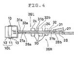
- FIG. 4shows an imaging device assembly according to another preferred embodiment of the present invention for an electronic stereoscopic endoscope system in which right and left circuit boards are disposed in an intermediate position of an imaging device in an vertical direction.
- the imaging device assemblycomprises right and left image pick-up modules (only the left image pick-up module 10 L is shown) disposed side by side with a predetermined slight distance and right and left circuit boards 26 R and 26 L.
- the right and left image pick-up modulesare substantially identical in structure, size and operation.
- the left image pick-up module 10 Lincludes a solid state image sensing element such as a CCD 11 , a cover glass plate 12 that is substantially the same in size as the CCD 11 and adhered to a front face of the CCD 11 , a mounting block 14 that is substantially the same in size as the CCD 11 and adhered to a rear face of the CCD 11 , and a number of wire leads 13 connected to CCD output terminals and extending across top and bottom faces of the CCD 11 and the mounting block 14 .
- the right and left image pick-up modulesare just the same in structure and size as those of the previous embodiment and need not be explained in more detail.
- the left circuit board 26 Lflexible or rigid, that is connected to the left image pick-up module 10 L in an approximately half height position
- the right circuit board 26 Rflexible or rigid, is connected to the right image pick-up module in an approximately half height position.
- These left and right circuit boards 26 R and 26 Lare the same in size and structure as those of the previous embodiment. That is, the right circuit board 26 R comprises upper and lower circuit boards 27 and 28 identical in shape with each other.
- the upper circuit board 27is divided into a front narrower board section 27 a having a width equal, or approximately equal, to a width of the CCD of the right image pick-up module and a rear broader board section 27 b having a width greater than the width of the front narrower board section 27 a but slightly smaller than an overall width of the imaging device comprising the right and left image pick-up modules arranged side by side at a predetermined slight distance.
- the lower circuit board 28is divided into a front narrower board section 28 a having the same width as the front narrower board section 27 a of the upper circuit board 27 and a rear broader board section 28 b having the same width as the rear broader board section 27 b of the upper circuit board 27 .
- These upper and lower circuit boards 27 and 28are separated from each other at the front narrower board sections 27 a and 28 a and, however, may or may not be adhered to each other at the rear broader board sections 27 b and 28 b.
- the left circuit board 26 Lcomprises upper and lower circuit boards 31 and 32 identical in shape with each other.
- the upper circuit board 31is divided into a front narrower board section 31 a having a width equal, or approximately equal, to a width of the CCD 11 of the left image pick-up module 10 L and a rear broader board section 31 b having a width greater than the width of the front narrower board section 31 a but slightly smaller than an overall width of the imaging device.
- the lower circuit board 32is divided into a front narrower board section 32 a having the same width as the front narrower board section 31 a of the upper circuit board 31 and a rear broader board section 32 b having the same width as the rear broader board section 31 b of the upper circuit board 31 .
- These upper and lower circuit boards 31 and 32are separated from each other at the front narrower board sections 31 a and 32 a and, however, may or may not be adhered to each other at the rear broader board sections 31 b and 32 b.
- the right circuit board 26 Rhas a given pattern of circuit printed, or otherwise fixedly formed, on and extending across all over the tops and reverses of the front narrower and rear broader board sections 27 a and 27 b of the upper circuit board 27 and a group of electronic parts 20 fixedly attached to the reverse of the rear broader board section 27 b of the upper circuit board 27 and incorporated in the circuit printed on the reverse of the upper circuit board 27 .
- the electronic parts 20are preferably arranged in a region of the rear broader board section 27 b projecting laterally from the front narrower board section 27 a of the upper circuit board 27 and incorporated in the circuit printed on the reverse of the upper circuit board 27 .
- the right circuit board 26 Rfurther has a given pattern of circuit printed, or otherwise fixedly formed, on the reverse of the lower circuit board 28 and extending across all over the reverses of the front narrower and rear broader board sections 28 a and 28 b of the lower circuit board 28 .
- the lower circuit board 28has openings formed in the rear broader board section 28 b corresponding in position and size to the electronic parts 20 fixedly attached to the rear broader board section 27 b of the upper circuit board 27 so that the electronic parts 20 are received in the openings, respectively, so as thereby to prevent the electronic parts 20 from mechanically interferes with the lower circuit board 28 when the upper and lower circuit boards 27 and 28 are laid to overlap closely each other.
- the left circuit board 26 Lhas a given pattern of circuit printed, or otherwise fixedly formed, on and extending across all over the tops of the front narrower and rear broader board sections 31 a and 31 b of the upper circuit board 31 and a group of electronic parts 24 fixedly attached to the top of the rear broader board section 31 b of the upper circuit board 31 and incorporated in the circuit printed on the tip of the upper circuit board 31 .
- the electronic parts 24include resistors, transistors, capacitors, etc. which are preferably arranged in a region of the rear broader board section 31 b projecting laterally from the front narrower board section 31 a of the upper circuit board 31 and incorporated in the circuit printed on the upper circuit board 31 .
- the left circuit board 26 Lfurther has a given pattern of circuit printed, or otherwise fixedly formed, on and extending across all over the reverses of the front narrower and rear broader board sections 32 of the lower circuit board 32 .
- the front narrower board section 31 a of the upper circuit board 31is bent upward and forward by a length approximately half the height of the left image pick-up module 10 L to take a reverse L-shaped form at the front extremity so as thereby to be tightly fitted to a rear profile of the mounting block 14 of the left image pick-up module 10 L.
- the front narrower board section 32 a of the lower circuit board 32is bent downward and forward by a length approximately half the height of the left image pick-up module 10 L to take an L-shaped form at the front extremity so as thereby to be tightly fitted to the rear profile of the mounting block 14 of the left image pick-up module 10 L.
- the left circuit board 26 Lis connected to the left image pick-up module 10 L by firmly adhering the reverse L-shaped end portion of the upper circuit board 31 to the top and back surfaces of the mounting block 14 and the L-shaped end portion of the lower circuit board 32 to the bottom and back surfaces of the mounting block 14 of the left image pick-up module 10 L.
- the L-shaped end portions of the front narrower board sections 31 a and 32 a of the upper and lower circuit boards 31 and 32extend to the top and the bottom of the CCD 11 of the left image pick-up module 10 L, respectively, beyond the mounting block 14 so that the wire leads 13 of the CCD 11 are connected to the circuit on the top of the upper circuit board 31 and the circuit on the reverse of the lower circuit board 32 .
- the right circuit board 26 Ris connected to the right image pick-up module in the same manner as applied to the left circuit board 26 L described above.
- the left circuit board 26 Lis placed right above the right circuit board 26 R so that the right and left circuit boards 26 R and 26 L overlap closely each other in a half height position of the imaging device.
- the right and left circuit boards 26 R and 26 L with circuits printed thereon and electronic parts 20 and 24are snugly enclosed within a tight space defined by and in the rear of the imaging device. Further, the electronic parts are placed on opposite sides of the right and left circuit boards 26 R and 26 L, it is allowed to incorporate bulky electronic parts in the imaging device assembly.
Landscapes
- Health & Medical Sciences (AREA)
- Life Sciences & Earth Sciences (AREA)
- Surgery (AREA)
- Engineering & Computer Science (AREA)
- Medical Informatics (AREA)
- Molecular Biology (AREA)
- Pathology (AREA)
- Radiology & Medical Imaging (AREA)
- Nuclear Medicine, Radiotherapy & Molecular Imaging (AREA)
- Biophysics (AREA)
- Biomedical Technology (AREA)
- Heart & Thoracic Surgery (AREA)
- Physics & Mathematics (AREA)
- Optics & Photonics (AREA)
- Animal Behavior & Ethology (AREA)
- General Health & Medical Sciences (AREA)
- Public Health (AREA)
- Veterinary Medicine (AREA)
- Multimedia (AREA)
- Signal Processing (AREA)
- Microelectronics & Electronic Packaging (AREA)
- Endoscopes (AREA)
- Instruments For Viewing The Inside Of Hollow Bodies (AREA)
- Studio Devices (AREA)
Abstract
Description
Claims (3)
Applications Claiming Priority (2)
| Application Number | Priority Date | Filing Date | Title |
|---|---|---|---|
| JP2003-44096 | 2003-02-21 | ||
| JP2003044096AJP3684365B2 (en) | 2003-02-21 | 2003-02-21 | 3D electronic endoscope imaging device |
Publications (2)
| Publication Number | Publication Date |
|---|---|
| US20040167378A1 US20040167378A1 (en) | 2004-08-26 |
| US6945929B2true US6945929B2 (en) | 2005-09-20 |
Family
ID=32866472
Family Applications (1)
| Application Number | Title | Priority Date | Filing Date |
|---|---|---|---|
| US10/781,903Expired - Fee RelatedUS6945929B2 (en) | 2003-02-21 | 2004-02-20 | Imaging device assembly for electronic stereoscopic endoscope system |
Country Status (2)
| Country | Link |
|---|---|
| US (1) | US6945929B2 (en) |
| JP (1) | JP3684365B2 (en) |
Cited By (44)
| Publication number | Priority date | Publication date | Assignee | Title |
|---|---|---|---|---|
| US20100022831A1 (en)* | 2008-07-22 | 2010-01-28 | Zhang Zifeng | Endoscope and a Method of Manufacturing the Same |
| US20110263942A1 (en)* | 2010-04-23 | 2011-10-27 | Medical Intubation Technology Corporation | Endoscope apparatus |
| USD716841S1 (en) | 2012-09-07 | 2014-11-04 | Covidien Lp | Display screen with annotate file icon |
| USD717340S1 (en) | 2012-09-07 | 2014-11-11 | Covidien Lp | Display screen with enteral feeding icon |
| US8926502B2 (en) | 2011-03-07 | 2015-01-06 | Endochoice, Inc. | Multi camera endoscope having a side service channel |
| USD735343S1 (en) | 2012-09-07 | 2015-07-28 | Covidien Lp | Console |
| US9101266B2 (en) | 2011-02-07 | 2015-08-11 | Endochoice Innovation Center Ltd. | Multi-element cover for a multi-camera endoscope |
| US9101287B2 (en) | 2011-03-07 | 2015-08-11 | Endochoice Innovation Center Ltd. | Multi camera endoscope assembly having multiple working channels |
| US9101268B2 (en) | 2009-06-18 | 2015-08-11 | Endochoice Innovation Center Ltd. | Multi-camera endoscope |
| US20150305606A1 (en)* | 2013-10-04 | 2015-10-29 | Olympus Corporation | Image pickup unit for endoscope |
| US9198835B2 (en) | 2012-09-07 | 2015-12-01 | Covidien Lp | Catheter with imaging assembly with placement aid and related methods therefor |
| US9314147B2 (en) | 2011-12-13 | 2016-04-19 | Endochoice Innovation Center Ltd. | Rotatable connector for an endoscope |
| US9320419B2 (en) | 2010-12-09 | 2016-04-26 | Endochoice Innovation Center Ltd. | Fluid channeling component of a multi-camera endoscope |
| US9402533B2 (en) | 2011-03-07 | 2016-08-02 | Endochoice Innovation Center Ltd. | Endoscope circuit board assembly |
| US9433339B2 (en) | 2010-09-08 | 2016-09-06 | Covidien Lp | Catheter with imaging assembly and console with reference library and related methods therefor |
| US9492063B2 (en) | 2009-06-18 | 2016-11-15 | Endochoice Innovation Center Ltd. | Multi-viewing element endoscope |
| US9517184B2 (en) | 2012-09-07 | 2016-12-13 | Covidien Lp | Feeding tube with insufflation device and related methods therefor |
| US9554692B2 (en) | 2009-06-18 | 2017-01-31 | EndoChoice Innovation Ctr. Ltd. | Multi-camera endoscope |
| US9560954B2 (en) | 2012-07-24 | 2017-02-07 | Endochoice, Inc. | Connector for use with endoscope |
| US9560953B2 (en) | 2010-09-20 | 2017-02-07 | Endochoice, Inc. | Operational interface in a multi-viewing element endoscope |
| US9642513B2 (en) | 2009-06-18 | 2017-05-09 | Endochoice Inc. | Compact multi-viewing element endoscope system |
| US9655502B2 (en) | 2011-12-13 | 2017-05-23 | EndoChoice Innovation Center, Ltd. | Removable tip endoscope |
| US9706903B2 (en) | 2009-06-18 | 2017-07-18 | Endochoice, Inc. | Multiple viewing elements endoscope system with modular imaging units |
| US9713417B2 (en) | 2009-06-18 | 2017-07-25 | Endochoice, Inc. | Image capture assembly for use in a multi-viewing elements endoscope |
| US20170251913A1 (en)* | 2016-03-01 | 2017-09-07 | Karl Storz Endovision, Inc. | Compact image sensor module and method of assembly for image sensor modules |
| US9814374B2 (en) | 2010-12-09 | 2017-11-14 | Endochoice Innovation Center Ltd. | Flexible electronic circuit board for a multi-camera endoscope |
| US9872609B2 (en) | 2009-06-18 | 2018-01-23 | Endochoice Innovation Center Ltd. | Multi-camera endoscope |
| US9901244B2 (en) | 2009-06-18 | 2018-02-27 | Endochoice, Inc. | Circuit board assembly of a multiple viewing elements endoscope |
| US9986899B2 (en) | 2013-03-28 | 2018-06-05 | Endochoice, Inc. | Manifold for a multiple viewing elements endoscope |
| US9993142B2 (en) | 2013-03-28 | 2018-06-12 | Endochoice, Inc. | Fluid distribution device for a multiple viewing elements endoscope |
| US10080486B2 (en) | 2010-09-20 | 2018-09-25 | Endochoice Innovation Center Ltd. | Multi-camera endoscope having fluid channels |
| US10165929B2 (en) | 2009-06-18 | 2019-01-01 | Endochoice, Inc. | Compact multi-viewing element endoscope system |
| US10203493B2 (en) | 2010-10-28 | 2019-02-12 | Endochoice Innovation Center Ltd. | Optical systems for multi-sensor endoscopes |
| US20190068859A1 (en)* | 2017-08-31 | 2019-02-28 | Fujikura Ltd. | Imaging module |
| US10499794B2 (en) | 2013-05-09 | 2019-12-10 | Endochoice, Inc. | Operational interface in a multi-viewing element endoscope |
| WO2020093138A1 (en)* | 2018-11-09 | 2020-05-14 | Titan Medical Inc. | Stereoscopic imaging apparatus for use in confined spaces |
| US11125990B2 (en)* | 2017-10-20 | 2021-09-21 | Olympus Corporation | Endoscope distal end portion, endoscope, and method of manufacturing endoscope distal end portion |
| US11278190B2 (en) | 2009-06-18 | 2022-03-22 | Endochoice, Inc. | Multi-viewing element endoscope |
| US11547275B2 (en) | 2009-06-18 | 2023-01-10 | Endochoice, Inc. | Compact multi-viewing element endoscope system |
| US11864734B2 (en) | 2009-06-18 | 2024-01-09 | Endochoice, Inc. | Multi-camera endoscope |
| US11889986B2 (en) | 2010-12-09 | 2024-02-06 | Endochoice, Inc. | Flexible electronic circuit board for a multi-camera endoscope |
| US12137873B2 (en) | 2009-06-18 | 2024-11-12 | Endochoice, Inc. | Compact multi-viewing element endoscope system |
| US12204087B2 (en) | 2010-10-28 | 2025-01-21 | Endochoice, Inc. | Optical systems for multi-sensor endoscopes |
| US12220105B2 (en) | 2010-06-16 | 2025-02-11 | Endochoice, Inc. | Circuit board assembly of a multiple viewing elements endoscope |
Families Citing this family (16)
| Publication number | Priority date | Publication date | Assignee | Title |
|---|---|---|---|---|
| DE102004056946A1 (en)* | 2004-11-23 | 2006-05-24 | Karl Storz Gmbh & Co. Kg | Image pick-up module and method of assembling an image pick-up module |
| JP2009082503A (en)* | 2007-09-28 | 2009-04-23 | Fujifilm Corp | Imaging apparatus and endoscope provided with the imaging apparatus |
| DE102012202133B4 (en)* | 2012-02-13 | 2022-02-17 | Olympus Winter & Ibe Gmbh | Electrical connector for a video endoscope, video endoscope and method for making an electrical connection in a video endoscope |
| JP5912058B2 (en) | 2012-03-30 | 2016-04-27 | 株式会社フジクラ | Imaging module, imaging module with lens, endoscope, imaging module manufacturing method, flexible wiring board molding apparatus |
| JP5961506B2 (en)* | 2012-09-27 | 2016-08-02 | 日立オートモティブシステムズ株式会社 | Stereo camera device |
| WO2014125070A1 (en) | 2013-02-15 | 2014-08-21 | Richard Wolf Gmbh | Assembly for a video endoscope |
| US20140300735A1 (en)* | 2013-04-09 | 2014-10-09 | Rsi Video Technologies, Inc. | Low-cost, compact security monitoring |
| JP2016522022A (en)* | 2013-04-29 | 2016-07-28 | エンドチョイス インコーポレイテッドEndochoice, Inc. | Video processing in small multi-view element endoscope system |
| JP2015002805A (en)* | 2013-06-19 | 2015-01-08 | オリンパス株式会社 | Endoscope |
| WO2014203604A1 (en)* | 2013-06-19 | 2014-12-24 | オリンパス株式会社 | Endoscope imaging unit |
| DE102014212712A1 (en)* | 2014-07-01 | 2016-01-07 | Olympus Winter & Ibe Gmbh | Video endoscope with flexible printed circuit board |
| US10451863B2 (en) | 2016-08-05 | 2019-10-22 | Verily Life Sciences Llc | Interposer for integration of multiple image sensors |
| DE112017006551T5 (en)* | 2016-12-26 | 2019-09-26 | Olympus Corporation | Stereo imaging unit |
| JP6342600B1 (en)* | 2016-12-26 | 2018-06-13 | オリンパス株式会社 | Stereo imaging unit |
| KR102586111B1 (en)* | 2018-02-22 | 2023-10-05 | 삼성에스디아이 주식회사 | Printed circuit board |
| CN116746862A (en)* | 2023-06-16 | 2023-09-15 | 广州瑞派医疗器械有限责任公司 | Imaging modules and endoscopes |
Citations (3)
| Publication number | Priority date | Publication date | Assignee | Title |
|---|---|---|---|---|
| US5603687A (en)* | 1992-10-28 | 1997-02-18 | Oktas General Partnership | Asymmetric stereo-optic endoscope |
| US5754313A (en)* | 1996-07-17 | 1998-05-19 | Welch Allyn, Inc. | Imager assembly |
| JP2000199863A (en) | 1999-01-07 | 2000-07-18 | Sony Corp | Solid-state image pickup device |
- 2003
- 2003-02-21JPJP2003044096Apatent/JP3684365B2/ennot_activeExpired - Fee Related
- 2004
- 2004-02-20USUS10/781,903patent/US6945929B2/ennot_activeExpired - Fee Related
Patent Citations (4)
| Publication number | Priority date | Publication date | Assignee | Title |
|---|---|---|---|---|
| US5603687A (en)* | 1992-10-28 | 1997-02-18 | Oktas General Partnership | Asymmetric stereo-optic endoscope |
| US5754313A (en)* | 1996-07-17 | 1998-05-19 | Welch Allyn, Inc. | Imager assembly |
| JP2000199863A (en) | 1999-01-07 | 2000-07-18 | Sony Corp | Solid-state image pickup device |
| US6567115B1 (en)* | 1999-01-07 | 2003-05-20 | Sony Corporation | Solid-state imaging device |
Cited By (85)
| Publication number | Priority date | Publication date | Assignee | Title |
|---|---|---|---|---|
| US8216127B2 (en)* | 2008-07-22 | 2012-07-10 | BYD Company Ltd. | Endoscope and a method of manufacturing the same |
| US20100022831A1 (en)* | 2008-07-22 | 2010-01-28 | Zhang Zifeng | Endoscope and a Method of Manufacturing the Same |
| US10905320B2 (en) | 2009-06-18 | 2021-02-02 | Endochoice, Inc. | Multi-camera endoscope |
| US10791909B2 (en) | 2009-06-18 | 2020-10-06 | Endochoice, Inc. | Image capture assembly for use in a multi-viewing elements endoscope |
| US12336686B2 (en) | 2009-06-18 | 2025-06-24 | Endochoice, Inc. | Multi-viewing element endoscope |
| US12303106B2 (en) | 2009-06-18 | 2025-05-20 | Endochoice, Inc. | Multi-camera endoscope |
| US9713417B2 (en) | 2009-06-18 | 2017-07-25 | Endochoice, Inc. | Image capture assembly for use in a multi-viewing elements endoscope |
| US12137873B2 (en) | 2009-06-18 | 2024-11-12 | Endochoice, Inc. | Compact multi-viewing element endoscope system |
| US11986155B2 (en) | 2009-06-18 | 2024-05-21 | Endochoice, Inc. | Multi-viewing element endoscope |
| US11864734B2 (en) | 2009-06-18 | 2024-01-09 | Endochoice, Inc. | Multi-camera endoscope |
| US9101268B2 (en) | 2009-06-18 | 2015-08-11 | Endochoice Innovation Center Ltd. | Multi-camera endoscope |
| US11547275B2 (en) | 2009-06-18 | 2023-01-10 | Endochoice, Inc. | Compact multi-viewing element endoscope system |
| US11534056B2 (en) | 2009-06-18 | 2022-12-27 | Endochoice, Inc. | Multi-camera endoscope |
| US11471028B2 (en) | 2009-06-18 | 2022-10-18 | Endochoice, Inc. | Circuit board assembly of a multiple viewing elements endoscope |
| US11278190B2 (en) | 2009-06-18 | 2022-03-22 | Endochoice, Inc. | Multi-viewing element endoscope |
| US10912445B2 (en) | 2009-06-18 | 2021-02-09 | Endochoice, Inc. | Compact multi-viewing element endoscope system |
| US9901244B2 (en) | 2009-06-18 | 2018-02-27 | Endochoice, Inc. | Circuit board assembly of a multiple viewing elements endoscope |
| US9872609B2 (en) | 2009-06-18 | 2018-01-23 | Endochoice Innovation Center Ltd. | Multi-camera endoscope |
| US10638922B2 (en) | 2009-06-18 | 2020-05-05 | Endochoice, Inc. | Multi-camera endoscope |
| US10791910B2 (en) | 2009-06-18 | 2020-10-06 | Endochoice, Inc. | Multiple viewing elements endoscope system with modular imaging units |
| US9706903B2 (en) | 2009-06-18 | 2017-07-18 | Endochoice, Inc. | Multiple viewing elements endoscope system with modular imaging units |
| US9554692B2 (en) | 2009-06-18 | 2017-01-31 | EndoChoice Innovation Ctr. Ltd. | Multi-camera endoscope |
| US10799095B2 (en) | 2009-06-18 | 2020-10-13 | Endochoice, Inc. | Multi-viewing element endoscope |
| US10765305B2 (en) | 2009-06-18 | 2020-09-08 | Endochoice, Inc. | Circuit board assembly of a multiple viewing elements endoscope |
| US9492063B2 (en) | 2009-06-18 | 2016-11-15 | Endochoice Innovation Center Ltd. | Multi-viewing element endoscope |
| US10165929B2 (en) | 2009-06-18 | 2019-01-01 | Endochoice, Inc. | Compact multi-viewing element endoscope system |
| US9642513B2 (en) | 2009-06-18 | 2017-05-09 | Endochoice Inc. | Compact multi-viewing element endoscope system |
| US10092167B2 (en) | 2009-06-18 | 2018-10-09 | Endochoice, Inc. | Multiple viewing elements endoscope system with modular imaging units |
| US9706905B2 (en) | 2009-06-18 | 2017-07-18 | Endochoice Innovation Center Ltd. | Multi-camera endoscope |
| US20110263942A1 (en)* | 2010-04-23 | 2011-10-27 | Medical Intubation Technology Corporation | Endoscope apparatus |
| US8414474B2 (en)* | 2010-04-23 | 2013-04-09 | Medical Intubation Technology Corporation | Multiple view angle endoscope apparatus |
| US12220105B2 (en) | 2010-06-16 | 2025-02-11 | Endochoice, Inc. | Circuit board assembly of a multiple viewing elements endoscope |
| US9538908B2 (en) | 2010-09-08 | 2017-01-10 | Covidien Lp | Catheter with imaging assembly |
| US9433339B2 (en) | 2010-09-08 | 2016-09-06 | Covidien Lp | Catheter with imaging assembly and console with reference library and related methods therefor |
| US9585813B2 (en) | 2010-09-08 | 2017-03-07 | Covidien Lp | Feeding tube system with imaging assembly and console |
| US10272016B2 (en) | 2010-09-08 | 2019-04-30 | Kpr U.S., Llc | Catheter with imaging assembly |
| US9560953B2 (en) | 2010-09-20 | 2017-02-07 | Endochoice, Inc. | Operational interface in a multi-viewing element endoscope |
| US9986892B2 (en) | 2010-09-20 | 2018-06-05 | Endochoice, Inc. | Operational interface in a multi-viewing element endoscope |
| US10080486B2 (en) | 2010-09-20 | 2018-09-25 | Endochoice Innovation Center Ltd. | Multi-camera endoscope having fluid channels |
| US10203493B2 (en) | 2010-10-28 | 2019-02-12 | Endochoice Innovation Center Ltd. | Optical systems for multi-sensor endoscopes |
| US12204087B2 (en) | 2010-10-28 | 2025-01-21 | Endochoice, Inc. | Optical systems for multi-sensor endoscopes |
| US11543646B2 (en) | 2010-10-28 | 2023-01-03 | Endochoice, Inc. | Optical systems for multi-sensor endoscopes |
| US10898063B2 (en) | 2010-12-09 | 2021-01-26 | Endochoice, Inc. | Flexible electronic circuit board for a multi camera endoscope |
| US11497388B2 (en) | 2010-12-09 | 2022-11-15 | Endochoice, Inc. | Flexible electronic circuit board for a multi-camera endoscope |
| US10182707B2 (en) | 2010-12-09 | 2019-01-22 | Endochoice Innovation Center Ltd. | Fluid channeling component of a multi-camera endoscope |
| US9320419B2 (en) | 2010-12-09 | 2016-04-26 | Endochoice Innovation Center Ltd. | Fluid channeling component of a multi-camera endoscope |
| US11889986B2 (en) | 2010-12-09 | 2024-02-06 | Endochoice, Inc. | Flexible electronic circuit board for a multi-camera endoscope |
| US9814374B2 (en) | 2010-12-09 | 2017-11-14 | Endochoice Innovation Center Ltd. | Flexible electronic circuit board for a multi-camera endoscope |
| US9101266B2 (en) | 2011-02-07 | 2015-08-11 | Endochoice Innovation Center Ltd. | Multi-element cover for a multi-camera endoscope |
| US10070774B2 (en) | 2011-02-07 | 2018-09-11 | Endochoice Innovation Center Ltd. | Multi-element cover for a multi-camera endoscope |
| US9351629B2 (en) | 2011-02-07 | 2016-05-31 | Endochoice Innovation Center Ltd. | Multi-element cover for a multi-camera endoscope |
| US11026566B2 (en) | 2011-03-07 | 2021-06-08 | Endochoice, Inc. | Multi camera endoscope assembly having multiple working channels |
| US9713415B2 (en) | 2011-03-07 | 2017-07-25 | Endochoice Innovation Center Ltd. | Multi camera endoscope having a side service channel |
| US9854959B2 (en) | 2011-03-07 | 2018-01-02 | Endochoice Innovation Center Ltd. | Multi camera endoscope assembly having multiple working channels |
| US8926502B2 (en) | 2011-03-07 | 2015-01-06 | Endochoice, Inc. | Multi camera endoscope having a side service channel |
| US10292578B2 (en) | 2011-03-07 | 2019-05-21 | Endochoice Innovation Center Ltd. | Multi camera endoscope assembly having multiple working channels |
| US9101287B2 (en) | 2011-03-07 | 2015-08-11 | Endochoice Innovation Center Ltd. | Multi camera endoscope assembly having multiple working channels |
| US9402533B2 (en) | 2011-03-07 | 2016-08-02 | Endochoice Innovation Center Ltd. | Endoscope circuit board assembly |
| US10470649B2 (en) | 2011-12-13 | 2019-11-12 | Endochoice, Inc. | Removable tip endoscope |
| US12290241B2 (en) | 2011-12-13 | 2025-05-06 | Endochoice, Inc. | Removable tip endoscope |
| US9655502B2 (en) | 2011-12-13 | 2017-05-23 | EndoChoice Innovation Center, Ltd. | Removable tip endoscope |
| US11291357B2 (en) | 2011-12-13 | 2022-04-05 | Endochoice, Inc. | Removable tip endoscope |
| US9314147B2 (en) | 2011-12-13 | 2016-04-19 | Endochoice Innovation Center Ltd. | Rotatable connector for an endoscope |
| US9560954B2 (en) | 2012-07-24 | 2017-02-07 | Endochoice, Inc. | Connector for use with endoscope |
| US9517184B2 (en) | 2012-09-07 | 2016-12-13 | Covidien Lp | Feeding tube with insufflation device and related methods therefor |
| USD716841S1 (en) | 2012-09-07 | 2014-11-04 | Covidien Lp | Display screen with annotate file icon |
| USD717340S1 (en) | 2012-09-07 | 2014-11-11 | Covidien Lp | Display screen with enteral feeding icon |
| USD735343S1 (en) | 2012-09-07 | 2015-07-28 | Covidien Lp | Console |
| US9198835B2 (en) | 2012-09-07 | 2015-12-01 | Covidien Lp | Catheter with imaging assembly with placement aid and related methods therefor |
| US11793393B2 (en) | 2013-03-28 | 2023-10-24 | Endochoice, Inc. | Manifold for a multiple viewing elements endoscope |
| US9986899B2 (en) | 2013-03-28 | 2018-06-05 | Endochoice, Inc. | Manifold for a multiple viewing elements endoscope |
| US12232699B2 (en) | 2013-03-28 | 2025-02-25 | Endochoice, Inc. | Manifold for a multiple viewing elements endoscope |
| US9993142B2 (en) | 2013-03-28 | 2018-06-12 | Endochoice, Inc. | Fluid distribution device for a multiple viewing elements endoscope |
| US10925471B2 (en) | 2013-03-28 | 2021-02-23 | Endochoice, Inc. | Fluid distribution device for a multiple viewing elements endoscope |
| US10905315B2 (en) | 2013-03-28 | 2021-02-02 | Endochoice, Inc. | Manifold for a multiple viewing elements endoscope |
| US11925323B2 (en) | 2013-03-28 | 2024-03-12 | Endochoice, Inc. | Fluid distribution device for a multiple viewing elements endoscope |
| US10499794B2 (en) | 2013-05-09 | 2019-12-10 | Endochoice, Inc. | Operational interface in a multi-viewing element endoscope |
| US9629524B2 (en)* | 2013-10-04 | 2017-04-25 | Olympus Corporation | Image pickup unit for endoscope having first and second leads with differing distances to image pickup device |
| US20150305606A1 (en)* | 2013-10-04 | 2015-10-29 | Olympus Corporation | Image pickup unit for endoscope |
| US20170251913A1 (en)* | 2016-03-01 | 2017-09-07 | Karl Storz Endovision, Inc. | Compact image sensor module and method of assembly for image sensor modules |
| US10485404B2 (en)* | 2016-03-01 | 2019-11-26 | Karl Storz Endovision, Inc. | Compact image sensor module and method of assembly for image sensor modules |
| US10757309B2 (en)* | 2017-08-31 | 2020-08-25 | Fujikura Ltd. | Endoscope imaging module with signal cable and flexible linear structure |
| US20190068859A1 (en)* | 2017-08-31 | 2019-02-28 | Fujikura Ltd. | Imaging module |
| US11125990B2 (en)* | 2017-10-20 | 2021-09-21 | Olympus Corporation | Endoscope distal end portion, endoscope, and method of manufacturing endoscope distal end portion |
| WO2020093138A1 (en)* | 2018-11-09 | 2020-05-14 | Titan Medical Inc. | Stereoscopic imaging apparatus for use in confined spaces |
Also Published As
| Publication number | Publication date |
|---|---|
| JP3684365B2 (en) | 2005-08-17 |
| JP2004248957A (en) | 2004-09-09 |
| US20040167378A1 (en) | 2004-08-26 |
Similar Documents
| Publication | Publication Date | Title |
|---|---|---|
| US6945929B2 (en) | Imaging device assembly for electronic stereoscopic endoscope system | |
| US9462933B2 (en) | Image pickup unit for endoscope | |
| US5633203A (en) | Method of making a miniaturized electronic imaging chip from a standard imaging chip | |
| JP4841391B2 (en) | Endoscope | |
| EP2687144B1 (en) | Imaging unit and endoscope | |
| US4757805A (en) | Endoscope | |
| KR100910175B1 (en) | 3D image sensor | |
| TWI611248B (en) | 360 degree panoramic camera module and apparatus | |
| WO2015019669A1 (en) | Imaging unit for endoscope | |
| CN211702154U (en) | Video camera | |
| US20100053391A1 (en) | Miniaturized image capturing device and method for assembling the same | |
| CN103685881B (en) | Camera module | |
| JP5197415B2 (en) | Electronics | |
| JP2014157309A (en) | Stereo camera unit | |
| JP5269157B2 (en) | Imaging device | |
| JPH10336496A (en) | Thin digital camera | |
| JP2008528094A (en) | Sensor with narrow assembly outline | |
| US6992724B2 (en) | Image-capture apparatus including light-guiding element having inclined surface | |
| JP4225141B2 (en) | The camera module | |
| JP4441305B2 (en) | The tip of the electronic endoscope | |
| CN109661192B (en) | Stereo camera unit | |
| KR101859380B1 (en) | Multi-camera device | |
| JP4459701B2 (en) | The tip of the electronic endoscope | |
| JP2012182409A (en) | Flexible wiring board, and drive circuit structure of electro-optical device | |
| JP4250480B2 (en) | Solid-state imaging device |
Legal Events
| Date | Code | Title | Description |
|---|---|---|---|
| AS | Assignment | Owner name:AI SYSTEMS, JAPAN Free format text:ASSIGNMENT OF ASSIGNORS INTEREST;ASSIGNOR:ANDO, KUNIO;REEL/FRAME:015010/0215 Effective date:20040209 Owner name:FUJI PHOTO OPTICAL CO., LTD., JAPAN Free format text:ASSIGNMENT OF ASSIGNORS INTEREST;ASSIGNOR:ANDO, KUNIO;REEL/FRAME:015010/0215 Effective date:20040209 | |
| AS | Assignment | Owner name:FUJINON CORPORATION, JAPAN Free format text:CHANGE OF NAME;ASSIGNOR:FUJI PHOTO OPTICAL CO., LTD.;REEL/FRAME:016549/0899 Effective date:20041001 Owner name:FUJINON CORPORATION,JAPAN Free format text:CHANGE OF NAME;ASSIGNOR:FUJI PHOTO OPTICAL CO., LTD.;REEL/FRAME:016549/0899 Effective date:20041001 | |
| FEPP | Fee payment procedure | Free format text:PAYER NUMBER DE-ASSIGNED (ORIGINAL EVENT CODE: RMPN); ENTITY STATUS OF PATENT OWNER: LARGE ENTITY Free format text:PAYOR NUMBER ASSIGNED (ORIGINAL EVENT CODE: ASPN); ENTITY STATUS OF PATENT OWNER: LARGE ENTITY | |
| FPAY | Fee payment | Year of fee payment:4 | |
| AS | Assignment | Owner name:FUJIFILM CORPORATION, JAPAN Free format text:ASSIGNMENT OF ASSIGNORS INTEREST;ASSIGNOR:FUJINON CORPORATION;REEL/FRAME:023379/0600 Effective date:20090907 | |
| FPAY | Fee payment | Year of fee payment:8 | |
| REMI | Maintenance fee reminder mailed | ||
| LAPS | Lapse for failure to pay maintenance fees | Free format text:PATENT EXPIRED FOR FAILURE TO PAY MAINTENANCE FEES (ORIGINAL EVENT CODE: EXP.) | |
| STCH | Information on status: patent discontinuation | Free format text:PATENT EXPIRED DUE TO NONPAYMENT OF MAINTENANCE FEES UNDER 37 CFR 1.362 | |
| FP | Lapsed due to failure to pay maintenance fee | Effective date:20170920 |