US6944731B2 - Dynamic random access memory system with bank conflict avoidance feature - Google Patents
Dynamic random access memory system with bank conflict avoidance featureDownload PDFInfo
- Publication number
- US6944731B2 US6944731B2US10/025,331US2533101AUS6944731B2US 6944731 B2US6944731 B2US 6944731B2US 2533101 AUS2533101 AUS 2533101AUS 6944731 B2US6944731 B2US 6944731B2
- Authority
- US
- United States
- Prior art keywords
- memory
- memory banks
- access
- banks
- requests
- Prior art date
- Legal status (The legal status is an assumption and is not a legal conclusion. Google has not performed a legal analysis and makes no representation as to the accuracy of the status listed.)
- Expired - Lifetime, expires
Links
Images


Classifications
- G—PHYSICS
- G06—COMPUTING OR CALCULATING; COUNTING
- G06F—ELECTRIC DIGITAL DATA PROCESSING
- G06F13/00—Interconnection of, or transfer of information or other signals between, memories, input/output devices or central processing units
- G06F13/14—Handling requests for interconnection or transfer
- G06F13/16—Handling requests for interconnection or transfer for access to memory bus
- G06F13/1605—Handling requests for interconnection or transfer for access to memory bus based on arbitration
- G06F13/1647—Handling requests for interconnection or transfer for access to memory bus based on arbitration with interleaved bank access
- G—PHYSICS
- G11—INFORMATION STORAGE
- G11C—STATIC STORES
- G11C7/00—Arrangements for writing information into, or reading information out from, a digital store
- Y—GENERAL TAGGING OF NEW TECHNOLOGICAL DEVELOPMENTS; GENERAL TAGGING OF CROSS-SECTIONAL TECHNOLOGIES SPANNING OVER SEVERAL SECTIONS OF THE IPC; TECHNICAL SUBJECTS COVERED BY FORMER USPC CROSS-REFERENCE ART COLLECTIONS [XRACs] AND DIGESTS
- Y02—TECHNOLOGIES OR APPLICATIONS FOR MITIGATION OR ADAPTATION AGAINST CLIMATE CHANGE
- Y02D—CLIMATE CHANGE MITIGATION TECHNOLOGIES IN INFORMATION AND COMMUNICATION TECHNOLOGIES [ICT], I.E. INFORMATION AND COMMUNICATION TECHNOLOGIES AIMING AT THE REDUCTION OF THEIR OWN ENERGY USE
- Y02D10/00—Energy efficient computing, e.g. low power processors, power management or thermal management
Definitions
- the present inventionrelates generally to memories for use in conjunction with network processors and other processing devices, and more particularly to a memory architecture configured for avoidance of conflict between multiple memory banks.
- a network processorgenerally controls the flow of packets between a physical transmission medium, such as a physical layer portion of, e.g., an asynchronous transfer mode (ATM) network or synchronous optical network (SONET), and a switch fabric in a router or other type of packet switch.
- a physical transmission mediumsuch as a physical layer portion of, e.g., an asynchronous transfer mode (ATM) network or synchronous optical network (SONET)
- ATMasynchronous transfer mode
- SONETsynchronous optical network
- DRAMs within or otherwise associated with a network processorare typically arranged in the form of multiple memory banks. Consecutive read or write accesses to an address or addresses within a given one of the banks will require waiting a random cycle time Trc for completion of a required access pre-charge process. However, consecutive accesses to even the same address within different banks do not experience this Trc wait time, which is also referred to herein as the bank conflict penalty.
- Static random access memoriesavoid the bank conflict penalty altogether. That is, any address in the memory can be accessed in a fixed time without incurring the Trc wait time associated with DRAMs.
- SRAMSStatic random access memories
- storage capacityis typically an order of magnitude lower, and their power consumption is typically two orders of magnitude higher, relative to comparably-sized DRAMs.
- FCDRAMfast cycle DRAM
- TC59LM814CFT-50A more particular example of an FCDRAM, commercially available from Toshiba, is identified by part number TC59LM814CFT-50.
- Trcthe random cycle time Trc is limited to 5T, where T denotes the memory clock period.
- the memory clock period Tis 5 nanoseconds and Trc is 25 nanoseconds, and the maximum data throughput using the four-burst mode is approximately 6.4 Gigabits per second (Gbps).
- GbpsGigabits per second
- the inventionprovides improved techniques for implementing DRAM-based memory suitable for use with a network processor or other processing device.
- a memory system having multiple memory banksis configured to prevent bank conflict between access requests.
- the memory systemincludes a memory controller and multiple memory banks operatively coupled to the memory controller, with each of the memory banks configured for storing a plurality of data items. More particularly, a given data item is stored as multiple copies of the data item with the multiple copies being stored in respective ones of a designated minimum number of the memory banks.
- the memory controlleris adapted to process requests for access to the data items stored in the memory banks in accordance with a specified bank access sequence, e.g., a round-robin sequence in which particular ones of the access requests are selected from head positions of a set of bank queues and applied to corresponding ones of the memory banks.
- the memory systemis configured to include at least first and second memory channels, with each of the channels including a number of memory banks storing the same set of data items.
- the above-noted memory controllerincludes a first controller coupled to each of the first channel of memory banks via a first set of address, data and control buses, and a second controller coupled to each of the second channel of memory banks via a second set of address, data and control buses.
- the memory controllerfurther includes a set of queues configured for storing the access requests, with each of the queues being associated with a corresponding one of the memory banks, and a memory access arbiter operatively coupled to the set of queues for selecting a given one of the access requests therefrom in accordance with the specified bank access sequence.
- the data throughput of a given embodimentmay be increased by increasing the number of channels of the memory system.
- the minimum number of memory banks for storage of the multiple copies of the given data itemmay be determined as a function of a random cycle time and a random bank access delay of the memory banks, e.g., as an integer greater than or equal to a ratio of the random cycle time to the random bank access delay.
- the memory systemis preferably operable in the above-described bank conflict avoidance mode as well as a standard random access mode.
- the particular operating mode of the systemmay be selected under program control via a host processor or other associated device.
- the memory systemis particularly well-suited for use in memory applications in which there is an unbalanced read/write ratio, i.e., memory applications typically involving substantially more read accesses than write accesses.
- One such memory applicationis as an external tree memory for a network processor integrated circuit.
- the inventioncan also be used in numerous other processing device memory applications.
- a memory system in accordance with the present inventioncan be configured to provide a maximum data throughput on the order of 10 Gbps or more.
- FIG. 1shows a simplified block diagram of a memory system configured in accordance with the techniques of the invention.
- FIG. 2illustrates the manner in which the same set of data items may be stored in multiple ones of the memory banks of the FIG. 1 memory system in a bank conflict avoidance mode in accordance with the invention.
- FIG. 3is a flow diagram of a bank conflict avoidance process in accordance with the invention.
- FIG. 4is a timing diagram showing the processing of access requests in the two channels of the FIG. 1 system in an illustrative embodiment of the invention.
- FIG. 5illustrates the use of the memory system of FIG. 1 as an external memory for a processing device which includes an internal memory.
- the inventionwill be illustrated herein in conjunction with an exemplary DRAM-based memory architecture particularly well-suited for use as an external memory in conjunction with a network processor. It should be understood, however, that the invention is more generally applicable to any processing device in which it is desirable to alleviate the above-described bank conflict penalty in multiple banks of internal or external random access memory.
- processing deviceas used herein is intended to include, by way of example and without limitation, network processors, microprocessors, central processing units (CPUs), digital signal processors (DSPs), application-specific integrated circuits (ASICs), and other types of data processing devices, as well as portions and combinations of these and other devices.
- network processorsmicroprocessors, central processing units (CPUs), digital signal processors (DSPs), application-specific integrated circuits (ASICs), and other types of data processing devices, as well as portions and combinations of these and other devices.
- CPUscentral processing units
- DSPsdigital signal processors
- ASICsapplication-specific integrated circuits
- the present inventionin an illustrative embodiment avoids the above-described bank conflict penalty in a multiple-bank DRAM-based memory system associated with a network processor or other processing device by storing a specified number of identical data copies in different memory banks of the system.
- the minimum number of data item copies neededis determined in the illustrative embodiment as a function of the random cycle time Trc and the random bank access delay Trbd of the DRAM devices used.
- the minimum number of data item copies for a given multiple-bank channel of the memory systemis determined as an integer number greater than or equal to a ratio of Trc to Trbd, such that if Trc is 25 nanoseconds, and Trbd is 10 nanoseconds, the number of identical copies of a given data item to be stored in different banks is three.
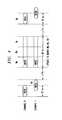
- FIG. 1shows a memory system 100 configured in accordance with the invention.
- the memory system 100includes a first channel 102 , also referred to herein as Channel 0 or Ch 0 , and a second channel 104 , also referred to herein as Channel 1 or Ch 1 .
- Each of the channels 102 and 104includes a set of N memory banks, denoted as banks B 0 , B 1 . . . BN.
- Channel 102further includes a Channel 0 memory controller 110 coupled to each of its associated Channel 0 banks B 0 , B 1 , . . . BN via an address bus 112 , a data bus 114 , and a control bus 116 as shown.
- channel 104further includes a Channel 1 memory controller 120 coupled to each of its associated Channel 1 banks B 0 , B 1 , . . . BN via an address bus 122 , a data bus 124 , and a control bus 126 .
- the memory system 100further includes a set of input first-in first-out (FIFO) queues 130 and a memory access arbiter 132 .
- FIFOinput first-in first-out
- the memory system 100may include decoder logic external to the memory banks, and such logic, although not shown in FIG. 1 , can process be configured to process address and control bus signals in a conventional manner.
- a separate set of such decoder logicmay be associated with each of the channels 102 and 104 , and may be wholly or partially incorporated into the associated memory controller 110 or 120 .
- the memory banks B 0 , B 1 , . . . BN of channels 102 and 104may each be implemented as one or more DRAM devices.
- the memory banksmay each be implemented as one or more of the fast cycle DRAM (FCDRAM) devices described previously. The manner in which such devices are configured is well-known in the art and will therefore not be described in further detail herein.
- FCDRAMfast cycle DRAM
- the present inventionis particularly well-suited for use in memory applications in which there is an unbalanced read/write ratio, i.e., memory applications typically involving substantially more read accesses than write accesses.
- An example of an application with an unbalanced read/write ratiois an application having 95% read accesses and 5% write accesses.
- the inventiondoes not require, however, any particular ratio of read and write accesses or type of unbalancing.
- the controllers 110 , 120 , queues 130 and access arbiter 132may be collectively viewed as a memory controller for the system 100 .
- the term “memory controller” as used hereinis therefore intended to be construed generally to encompass a single channel controller such as controller 110 or 120 , or a more complex configuration including multiple channel controllers, as well as one or more arbiters, queues, or other related elements.
- memory system 100as shown in FIG. 1 is by way of example only, and should not be construed as limiting the scope of the invention to any particular embodiment or group of embodiments.
- memory system 100as shown in FIG. 1 is by way of example only, and should not be construed as limiting the scope of the invention to any particular embodiment or group of embodiments.
- memory system 100although shown as including two channels each with N memory banks, those skilled in the art will appreciate that the invention can be implemented using more than two channels or only a single channel, and that in a given multiple-channel embodiment each channel need not have the same number of memory banks.
- the data throughput of a given embodimentmay be increased by increasing the number of channels of the memory system. In other words, the data throughput is proportional to the number of channels used.
- input access requestsare directed to particular ones of the FIFO queues 130 .
- These queuesare preferably organized by bank, such that requests directed to a particular one of the Channel 0 or Channel 1 banks are stored within a particular FIFO queue associated with that bank in the set of FIFO queues 130 .
- the memory access arbiter 132selects access requests from the FIFO queues 130 in accordance with a specified bank access sequence configured to prevent the previously-described bank conflict problem between access requests directed to different banks. Examples of this sequencing will be described in greater detail below.
- each of the access requests to be stored in the FIFO queues 130involves reading a particular data item from a specified address within a given one of the banks.
- the memory system 100is configurable in accordance with the techniques of the present invention to be operable in the above-noted bank conflict avoidance mode. In this mode, a specified number of identical data copies are stored in different ones of the banks B 0 , B 1 , . . . BN, in each of the channels 102 and 104 .
- the minimum number of data item copies neededis determined in the illustrative embodiment as a function of the random cycle time Trc and the random bank access delay Trbd of the particular DRAM devices used in the Channel 0 and Channel 1 banks B 0 , B 1 , . . . BN. More particularly, the minimum number of the memory banks for storage of the multiple copies of a given data item is determined as an integer greater than or equal to a ratio of the random cycle time Trc to the random bank access delay Trbd. In the example given above, the minimum number of data item copies is determined as an integer number greater than or equal to a ratio of Trc to Trbd. Therefore, if the particular DRAM devices used have a Trc of 25 nanoseconds, and a Trbd of 10 nanoseconds, the number of identical copies of a given data item to be stored in different banks of a given memory channel is three.
- FIG. 2illustrates the maimer in which multiple copies of data items are stored in a designated minimum number of memory banks in the bank conflict avoidance mode.
- each of the banks B 0 , B 1 and B 2 of the N banks in a given channelstores the same set of K data items, denoted data item 1 , data item 2 , . . . data item K.
- the same storage configurationis utilized in both channel 102 and channel 104 , such that a total of six banks out of the 2N total number of banks store the same set of data items.
- Each of the data items in this examplecorresponds to a particular addressable word of a memory bank.
- the above-noted input access requestsare preferably directed to such addressable words within a particular one of the memory banks.
- FIG. 3is a flow diagram of a bank conflict avoidance process that may be implemented in the FIG. 1 system using the techniques of the invention.
- the systementers bank conflict avoidance mode. This can be accomplished by programmable configuration of the controllers 110 , 120 , queues 130 and arbiter 132 , as will be apparent to those skilled in the art.
- Step 302indicates that the same set of data items are then stored in the minimum number of banks in each channel, in the manner described previously.
- the minimum number of banksmay be predetermined based on a given known memory system configuration, or may be dynamically determined using logic circuitry within the system memory controller.
- the access requestsare selected in a round-robin sequence from head positions of the sets of queues 130 and applied to corresponding ones of the memory banks.
- the access requestsmay be selected based on the following bank access sequence pattern: Ch 0 -B 0 , Ch 1 -B 0 , Ch 0 -B 1 , Ch 1 -B 1 , Ch 0 -B 2 , Ch 1 -B 2 , Ch 0 -B 0 , Ch 1 -B 0 , and so on.
- Other combinations of channel and bankmay be used in other bank access sequences suitable for use in accordance with the present invention.
- FIG. 4is a timing diagram illustrating the processing of a number of different access requests, using the above-described bank conflict avoidance mode, in the two channels 102 , 104 of the FIG. 1 system. It is again assumed that duplicate sets of data items are stored in each of the banks B 0 , B 1 and B 2 of each of Channel 0 and Channel 1 , as described in conjunction with FIG. 2 . In this example timing diagram, it can be seen that read access requests each take approximately 10 nanoseconds. This corresponds to the above-noted random bank access delay Trbd.
- the Channe 10 and Channe 11 banksare totally independent in this illustrative embodiment.
- a read access request for a particular bank in Channel 0may therefore overlap with a read access request for a particular bank in Channel 1 , as illustrated in the figure, although this type of staggering is by way of example only and not a requirement of the invention.
- the FIG. 4 timing diagramalso shows 30 nanoseconds of write access requests that are used to update the contents of the banks B 0 , B 1 and B 2 .
- the random cycle time Trc in this exampleis assumed to be 25 nanoseconds. It should be emphasized that the particular timing intervals shown in the figure are examples only.
- a delay less than or equal to Trcis incurred before and after the example set of write access requests shown in FIG. 4 .
- the memory systemmay include additional logic which reduces the actual wait time in a given embodiment.
- additional logiccan be configured to determine the particular ordering of the write accesses to banks Ba, Bb and Bc in FIG. 4 based on the last read access (to bank Bx) before the update and the first read access (to bank By) after the update, where a, b, c, x and y may take on the values 0, 1 or 2 in this example.
- each channelmay be configured to include 4 banks, with the same data items stored in three of the four banks as previously described.
- the DRAM devicesmay be the above-noted FCDRAM devices identified by part number TC59LM814CFT-50 and commercially available from Toshiba, operating in the four-burst mode, using a 200 MHz memory clock, with each of the banks including 4M memory words of 16 bits each.
- DRAM memory banks suitable for use in conjunction with the present inventioninclude, by way of example and not limitation, part numbers TC59LM806CFT-50, TC59LM806BFT-22 and TC59LM814BFT-22 from Toshiba and part numbers MB81N251647-50 and MB81N25847-50 from Fujitsu, although the maximum achievable data throughput may vary depending upon the devices used.
- the memory system 100is preferably operable in multiple modes, including the above-described bank conflict avoidance mode, and at least one other mode.
- This other modemay be a conventional DRAM operating mode, in which the memory system 100 operates substantially as a conventional DRAM-based system and is therefore subject to the bank conflict penalty previously described.
- each of the banks B 0 , B 1 , . . . BN in each of the channels 102 , 104may store a different set of data items, and the data items may be accessed in a random manner. In other words, the specified bank access sequencing associated with the bank conflict avoidance mode is not used.
- DRAM operationsthat may be implemented in the system 100 are well-understood in the art, and are therefore not described in detail herein. It is also possible in the DRAM operating mode to utilize particular techniques for scheduling random accesses so as to minimize the impact of the bank conflict penalty.
- the particular operating mode of the system 100may be selected under program control in a straightforward manner.
- FIG. 5shows an example processing system in which the memory system 100 may be implemented in accordance with the techniques of the invention.
- the processing systemcomprises a line card 500 having an integrated circuit 502 installed thereon.
- the integrated circuit 502comprises a processing device 504 having an internal memory 506 .
- the processing device 504interacts with an external memory on the line card 500 .
- the external memoryis the memory system 100 illustrated and described in conjunction with FIG. 1 .
- the processing system as shown in FIG. 5is considerably simplified for clarity of illustration. It is to be appreciated, however, that the processing system may comprise a router or switch which includes multiple such line cards, and that each of the line cards may include multiple integrated circuits. Similar implementations of the invention may be based on one or more port cards of a router or switch.
- the processing device 504may comprise a network processor.
- the memory system 100is particularly well-suited for use in memory applications in which there is an unbalanced read/write ratio, i.e., memory applications typically involving substantially more read accesses than write accesses.
- the memory system 100may serve, e.g., as an external tree memory for the network processor integrated circuit.
- a tree memoryis used in conjunction with a binary or non-binary tree search algorithm which attempts to determine the presence or absence of a match between a search object and a particular stored data item.
- An example of a non-binary tree search algorithm known in the artis described in U.S. Pat. No.
- the memory system 100 of the present inventioncan be utilized in numerous other applications and a wide variety of other processing system configurations.
- the memory system 100can be utilized as an internal memory in a network processor or other processing device.
- the above-described embodiments of the inventionare intended to be illustrative only.
- the present inventioncan be implemented using other configurations of memory system elements.
- the minimum number of memory banks required for storage of multiple copies of a given data itemmay be determined as another function of the random cycle time of the memory banks, the random bank access delay of the memory banks, or a combination of both.
- the illustrative embodimentsutilize two independent memory channels, each having data copies stored in a minimum of three memory banks, and with each bank storing the identical data items, it should be appreciated that other numbers of channels, banks per channel and distribution of data copies over the banks may be used.
Landscapes
- Engineering & Computer Science (AREA)
- Theoretical Computer Science (AREA)
- Physics & Mathematics (AREA)
- General Engineering & Computer Science (AREA)
- General Physics & Mathematics (AREA)
- Dram (AREA)
- Memory System (AREA)
- Multi Processors (AREA)
Abstract
Description
Claims (18)
Priority Applications (5)
| Application Number | Priority Date | Filing Date | Title |
|---|---|---|---|
| US10/025,331US6944731B2 (en) | 2001-12-19 | 2001-12-19 | Dynamic random access memory system with bank conflict avoidance feature |
| EP02258105.2AEP1345125B1 (en) | 2001-12-19 | 2002-11-25 | Dynamic random access memory system with bank conflict avoidance feature |
| TW091134318ATWI255990B (en) | 2001-12-19 | 2002-11-26 | Memory system and processing system for avoiding bank conflict and method therefor |
| JP2002364520AJP4369660B2 (en) | 2001-12-19 | 2002-12-17 | Dynamic random access memory system with bank collision avoidance function |
| KR1020020081396AKR100963721B1 (en) | 2001-12-19 | 2002-12-18 | Memory system, processing system and how to use in memory system |
Applications Claiming Priority (1)
| Application Number | Priority Date | Filing Date | Title |
|---|---|---|---|
| US10/025,331US6944731B2 (en) | 2001-12-19 | 2001-12-19 | Dynamic random access memory system with bank conflict avoidance feature |
Publications (2)
| Publication Number | Publication Date |
|---|---|
| US20030115403A1 US20030115403A1 (en) | 2003-06-19 |
| US6944731B2true US6944731B2 (en) | 2005-09-13 |
Family
ID=21825396
Family Applications (1)
| Application Number | Title | Priority Date | Filing Date |
|---|---|---|---|
| US10/025,331Expired - LifetimeUS6944731B2 (en) | 2001-12-19 | 2001-12-19 | Dynamic random access memory system with bank conflict avoidance feature |
Country Status (5)
| Country | Link |
|---|---|
| US (1) | US6944731B2 (en) |
| EP (1) | EP1345125B1 (en) |
| JP (1) | JP4369660B2 (en) |
| KR (1) | KR100963721B1 (en) |
| TW (1) | TWI255990B (en) |
Cited By (13)
| Publication number | Priority date | Publication date | Assignee | Title |
|---|---|---|---|---|
| US20030161315A1 (en)* | 2002-02-27 | 2003-08-28 | International Business Machines Corporation | Memory system with apparatus and method to enable balanced bandwidth utilization |
| US20050004998A1 (en)* | 2001-07-18 | 2005-01-06 | Hitachi, Ltd. | Storage subsystem |
| US20060156102A1 (en)* | 2005-01-11 | 2006-07-13 | Johnson Tyler J | System and method to control data capture |
| US20060155516A1 (en)* | 2005-01-11 | 2006-07-13 | Johnson Tyler J | System and method for data analysis |
| US20060156290A1 (en)* | 2005-01-11 | 2006-07-13 | Johnson Tyler J | System and method to qualify data capture |
| US20070011409A1 (en)* | 2005-07-05 | 2007-01-11 | Arm Limited | Memory controller |
| US20070180216A1 (en)* | 2006-01-31 | 2007-08-02 | Brown David A | Processor with programmable configuration of logical-to-physical address translation on a per-client basis |
| US20070198782A1 (en)* | 2006-02-23 | 2007-08-23 | Sved Jorge A | Memory controller |
| US20090037641A1 (en)* | 2007-07-31 | 2009-02-05 | Bresniker Kirk M | Memory controller with multi-protocol interface |
| US20100161892A1 (en)* | 2008-12-19 | 2010-06-24 | Fulcrum Microsystems, Inc. | Pseudo dual-ported sram |
| US20100217915A1 (en)* | 2009-02-23 | 2010-08-26 | International Business Machines Corporation | High availability memory system |
| US8090901B2 (en) | 2009-05-14 | 2012-01-03 | Brocade Communications Systems, Inc. | TCAM management approach that minimize movements |
| US9361973B2 (en) | 2013-10-28 | 2016-06-07 | Cypress Semiconductor Corporation | Multi-channel, multi-bank memory with wide data input/output |
Families Citing this family (71)
| Publication number | Priority date | Publication date | Assignee | Title |
|---|---|---|---|---|
| US7596139B2 (en) | 2000-11-17 | 2009-09-29 | Foundry Networks, Inc. | Backplane interface adapter with error control and redundant fabric |
| US7236490B2 (en) | 2000-11-17 | 2007-06-26 | Foundry Networks, Inc. | Backplane interface adapter |
| US6839797B2 (en)* | 2001-12-21 | 2005-01-04 | Agere Systems, Inc. | Multi-bank scheduling to improve performance on tree accesses in a DRAM based random access memory subsystem |
| US7468975B1 (en) | 2002-05-06 | 2008-12-23 | Foundry Networks, Inc. | Flexible method for processing data packets in a network routing system for enhanced efficiency and monitoring capability |
| US7266117B1 (en) | 2002-05-06 | 2007-09-04 | Foundry Networks, Inc. | System architecture for very fast ethernet blade |
| US7187687B1 (en) | 2002-05-06 | 2007-03-06 | Foundry Networks, Inc. | Pipeline method and system for switching packets |
| US20120155466A1 (en) | 2002-05-06 | 2012-06-21 | Ian Edward Davis | Method and apparatus for efficiently processing data packets in a computer network |
| US7649885B1 (en) | 2002-05-06 | 2010-01-19 | Foundry Networks, Inc. | Network routing system for enhanced efficiency and monitoring capability |
| US6901072B1 (en) | 2003-05-15 | 2005-05-31 | Foundry Networks, Inc. | System and method for high speed packet transmission implementing dual transmit and receive pipelines |
| US7167942B1 (en)* | 2003-06-09 | 2007-01-23 | Marvell International Ltd. | Dynamic random access memory controller |
| US7360026B1 (en)* | 2003-10-06 | 2008-04-15 | Altera Corporation | Method and apparatus for synchronizing data with a reduced clock cycle response time |
| US20050138276A1 (en)* | 2003-12-17 | 2005-06-23 | Intel Corporation | Methods and apparatus for high bandwidth random access using dynamic random access memory |
| JP4534488B2 (en)* | 2004-01-05 | 2010-09-01 | ソニー株式会社 | Data storage device, data storage control device, data storage control method, and data storage control program |
| US7817659B2 (en) | 2004-03-26 | 2010-10-19 | Foundry Networks, Llc | Method and apparatus for aggregating input data streams |
| JP4735008B2 (en)* | 2004-04-19 | 2011-07-27 | ソニー株式会社 | Data storage device, data storage control device, data storage control method, and data storage control program |
| US8730961B1 (en) | 2004-04-26 | 2014-05-20 | Foundry Networks, Llc | System and method for optimizing router lookup |
| US7277982B2 (en)* | 2004-07-27 | 2007-10-02 | International Business Machines Corporation | DRAM access command queuing structure |
| DK1794979T3 (en)* | 2004-09-10 | 2017-07-24 | Cavium Inc | Selective copying of data structure |
| US7594081B2 (en) | 2004-09-10 | 2009-09-22 | Cavium Networks, Inc. | Direct access to low-latency memory |
| US7941585B2 (en)* | 2004-09-10 | 2011-05-10 | Cavium Networks, Inc. | Local scratchpad and data caching system |
| US7657703B1 (en) | 2004-10-29 | 2010-02-02 | Foundry Networks, Inc. | Double density content addressable memory (CAM) lookup scheme |
| US7801174B2 (en)* | 2004-12-29 | 2010-09-21 | Alcatel-Lucent Usa Inc. | Techniques for efficient control of aggregating wireless voice communications |
| US8448162B2 (en) | 2005-12-28 | 2013-05-21 | Foundry Networks, Llc | Hitless software upgrades |
| US7903654B2 (en) | 2006-08-22 | 2011-03-08 | Foundry Networks, Llc | System and method for ECMP load sharing |
| US8238255B2 (en) | 2006-11-22 | 2012-08-07 | Foundry Networks, Llc | Recovering from failures without impact on data traffic in a shared bus architecture |
| US7949841B2 (en)* | 2006-12-08 | 2011-05-24 | Microsoft Corporation | Protection of critical memory using replication |
| US8155011B2 (en) | 2007-01-11 | 2012-04-10 | Foundry Networks, Llc | Techniques for using dual memory structures for processing failure detection protocol packets |
| US8327057B1 (en) | 2007-04-16 | 2012-12-04 | Juniper Networks, Inc. | Ordering write bursts to memory |
| US8037399B2 (en) | 2007-07-18 | 2011-10-11 | Foundry Networks, Llc | Techniques for segmented CRC design in high speed networks |
| US8271859B2 (en) | 2007-07-18 | 2012-09-18 | Foundry Networks Llc | Segmented CRC design in high speed networks |
| US8099564B1 (en)* | 2007-08-10 | 2012-01-17 | Xilinx, Inc. | Programmable memory controller |
| US8509236B2 (en) | 2007-09-26 | 2013-08-13 | Foundry Networks, Llc | Techniques for selecting paths and/or trunk ports for forwarding traffic flows |
| US8254191B2 (en)* | 2008-10-30 | 2012-08-28 | Micron Technology, Inc. | Switched interface stacked-die memory architecture |
| US8599850B2 (en) | 2009-09-21 | 2013-12-03 | Brocade Communications Systems, Inc. | Provisioning single or multistage networks using ethernet service instances (ESIs) |
| US8293198B2 (en)* | 2009-12-18 | 2012-10-23 | Basf Corporation | Process of direct copper exchange into Na+-form of chabazite molecular sieve, and catalysts, systems and methods |
| US9612775B1 (en)* | 2009-12-30 | 2017-04-04 | Micron Technology, Inc. | Solid state drive controller |
| US9442866B1 (en) | 2009-12-30 | 2016-09-13 | Micron Technology | Self-adaptive solid state drive controller |
| US10229139B2 (en) | 2011-08-02 | 2019-03-12 | Cavium, Llc | Incremental update heuristics |
| CN102681946B (en)* | 2012-05-11 | 2015-03-11 | 龙芯中科技术有限公司 | Memory access method and device |
| US10083200B2 (en) | 2013-03-14 | 2018-09-25 | Cavium, Inc. | Batch incremental update |
| US9430511B2 (en)* | 2013-03-15 | 2016-08-30 | Cavium, Inc. | Merging independent writes, separating dependent and independent writes, and error roll back |
| US9195939B1 (en) | 2013-03-15 | 2015-11-24 | Cavium, Inc. | Scope in decision trees |
| US9595003B1 (en) | 2013-03-15 | 2017-03-14 | Cavium, Inc. | Compiler with mask nodes |
| US9652415B2 (en)* | 2014-07-09 | 2017-05-16 | Sandisk Technologies Llc | Atomic non-volatile memory data transfer |
| US9904621B2 (en) | 2014-07-15 | 2018-02-27 | Sandisk Technologies Llc | Methods and systems for flash buffer sizing |
| US9645744B2 (en) | 2014-07-22 | 2017-05-09 | Sandisk Technologies Llc | Suspending and resuming non-volatile memory operations |
| US9436397B2 (en) | 2014-09-23 | 2016-09-06 | Sandisk Technologies Llc. | Validating the status of memory operations |
| US9753649B2 (en) | 2014-10-27 | 2017-09-05 | Sandisk Technologies Llc | Tracking intermix of writes and un-map commands across power cycles |
| US9952978B2 (en) | 2014-10-27 | 2018-04-24 | Sandisk Technologies, Llc | Method for improving mixed random performance in low queue depth workloads |
| US9558125B2 (en) | 2014-10-27 | 2017-01-31 | Sandisk Technologies Llc | Processing of un-map commands to enhance performance and endurance of a storage device |
| US9824007B2 (en) | 2014-11-21 | 2017-11-21 | Sandisk Technologies Llc | Data integrity enhancement to protect against returning old versions of data |
| US9817752B2 (en) | 2014-11-21 | 2017-11-14 | Sandisk Technologies Llc | Data integrity enhancement to protect against returning old versions of data |
| CN105760315A (en)* | 2014-12-15 | 2016-07-13 | 深圳市中兴微电子技术有限公司 | Method and device improving synchronization dynamic RAM access efficiency |
| US9647697B2 (en) | 2015-03-16 | 2017-05-09 | Sandisk Technologies Llc | Method and system for determining soft information offsets |
| US9652175B2 (en) | 2015-04-09 | 2017-05-16 | Sandisk Technologies Llc | Locally generating and storing RAID stripe parity with single relative memory address for storing data segments and parity in multiple non-volatile memory portions |
| US9864545B2 (en) | 2015-04-14 | 2018-01-09 | Sandisk Technologies Llc | Open erase block read automation |
| US9753653B2 (en) | 2015-04-14 | 2017-09-05 | Sandisk Technologies Llc | High-priority NAND operations management |
| US10372529B2 (en) | 2015-04-20 | 2019-08-06 | Sandisk Technologies Llc | Iterative soft information correction and decoding |
| US9778878B2 (en) | 2015-04-22 | 2017-10-03 | Sandisk Technologies Llc | Method and system for limiting write command execution |
| US10241941B2 (en) | 2015-06-29 | 2019-03-26 | Nxp Usa, Inc. | Systems and methods for asymmetric memory access to memory banks within integrated circuit systems |
| US9870149B2 (en) | 2015-07-08 | 2018-01-16 | Sandisk Technologies Llc | Scheduling operations in non-volatile memory devices using preference values |
| US9715939B2 (en) | 2015-08-10 | 2017-07-25 | Sandisk Technologies Llc | Low read data storage management |
| US10228990B2 (en) | 2015-11-12 | 2019-03-12 | Sandisk Technologies Llc | Variable-term error metrics adjustment |
| US10126970B2 (en) | 2015-12-11 | 2018-11-13 | Sandisk Technologies Llc | Paired metablocks in non-volatile storage device |
| US9837146B2 (en) | 2016-01-08 | 2017-12-05 | Sandisk Technologies Llc | Memory system temperature management |
| US10732856B2 (en) | 2016-03-03 | 2020-08-04 | Sandisk Technologies Llc | Erase health metric to rank memory portions |
| US10481830B2 (en) | 2016-07-25 | 2019-11-19 | Sandisk Technologies Llc | Selectively throttling host reads for read disturbs in non-volatile memory system |
| JP2019091191A (en) | 2017-11-14 | 2019-06-13 | ルネサスエレクトロニクス株式会社 | Semiconductor device, data processing system, data reading method and data reading program |
| US11422707B2 (en)* | 2017-12-21 | 2022-08-23 | Advanced Micro Devices, Inc. | Scheduling memory requests for a ganged memory device |
| US10679320B1 (en)* | 2018-07-23 | 2020-06-09 | Ambarella International Lp | High dynamic range sensor system with row increment operation |
| CN110187835B (en)* | 2019-05-24 | 2023-02-03 | 北京百度网讯科技有限公司 | Method, device, device and storage medium for managing access requests |
Citations (6)
| Publication number | Priority date | Publication date | Assignee | Title |
|---|---|---|---|---|
| US4766535A (en)* | 1985-12-20 | 1988-08-23 | International Business Machines Corporation | High-performance multiple port memory |
| US4912698A (en)* | 1983-09-26 | 1990-03-27 | Siemens Aktiengesellschaft | Multi-processor central control unit of a telephone exchange system and its operation |
| US6108243A (en)* | 1998-08-26 | 2000-08-22 | Fujitsu Limited | High-speed random access memory device |
| US6308219B1 (en)* | 1998-07-31 | 2001-10-23 | Cisco Technology, Inc. | Routing table lookup implemented using M-trie having nodes duplicated in multiple memory banks |
| US6430527B1 (en)* | 1998-05-06 | 2002-08-06 | Avici Systems | Prefix search circuitry and method |
| US6636445B2 (en)* | 1999-12-13 | 2003-10-21 | Kabushiki Kaisha Toshiba | Fast cycle ram having improved data write operation |
Family Cites Families (2)
| Publication number | Priority date | Publication date | Assignee | Title |
|---|---|---|---|---|
| US5966143A (en)* | 1997-10-14 | 1999-10-12 | Motorola, Inc. | Data allocation into multiple memories for concurrent access |
| US6088771A (en)* | 1997-10-24 | 2000-07-11 | Digital Equipment Corporation | Mechanism for reducing latency of memory barrier operations on a multiprocessor system |
- 2001
- 2001-12-19USUS10/025,331patent/US6944731B2/ennot_activeExpired - Lifetime
- 2002
- 2002-11-25EPEP02258105.2Apatent/EP1345125B1/ennot_activeExpired - Lifetime
- 2002-11-26TWTW091134318Apatent/TWI255990B/ennot_activeIP Right Cessation
- 2002-12-17JPJP2002364520Apatent/JP4369660B2/ennot_activeExpired - Fee Related
- 2002-12-18KRKR1020020081396Apatent/KR100963721B1/ennot_activeExpired - Fee Related
Patent Citations (6)
| Publication number | Priority date | Publication date | Assignee | Title |
|---|---|---|---|---|
| US4912698A (en)* | 1983-09-26 | 1990-03-27 | Siemens Aktiengesellschaft | Multi-processor central control unit of a telephone exchange system and its operation |
| US4766535A (en)* | 1985-12-20 | 1988-08-23 | International Business Machines Corporation | High-performance multiple port memory |
| US6430527B1 (en)* | 1998-05-06 | 2002-08-06 | Avici Systems | Prefix search circuitry and method |
| US6308219B1 (en)* | 1998-07-31 | 2001-10-23 | Cisco Technology, Inc. | Routing table lookup implemented using M-trie having nodes duplicated in multiple memory banks |
| US6108243A (en)* | 1998-08-26 | 2000-08-22 | Fujitsu Limited | High-speed random access memory device |
| US6636445B2 (en)* | 1999-12-13 | 2003-10-21 | Kabushiki Kaisha Toshiba | Fast cycle ram having improved data write operation |
Non-Patent Citations (2)
| Title |
|---|
| Davis et al., The New DRAM Interfaces; SDRAM, DRDRAM amd Variants, Oct. 2000, High Performance Computing, 3<SUP>rd </SUP>ed. Int Symp.* |
| Sato et al., Fast Cycle RAM (FCRAM); a 20-ns Random Row Access, Pipe-Lined Operating DRAM, 1998, Symp. on VLSI Circuits Digest of Technical Papers.* |
Cited By (26)
| Publication number | Priority date | Publication date | Assignee | Title |
|---|---|---|---|---|
| US20050004998A1 (en)* | 2001-07-18 | 2005-01-06 | Hitachi, Ltd. | Storage subsystem |
| US6996607B2 (en)* | 2001-07-18 | 2006-02-07 | Hitachi, Ltd. | Storage subsystem and method employing load balancing |
| US20030161315A1 (en)* | 2002-02-27 | 2003-08-28 | International Business Machines Corporation | Memory system with apparatus and method to enable balanced bandwidth utilization |
| US7944931B2 (en) | 2002-02-27 | 2011-05-17 | International Business Machines Corporation | Balanced bandwidth utilization |
| US7286543B2 (en)* | 2002-02-27 | 2007-10-23 | International Business Machines Corporation | Memory system with apparatus and method to enable balanced bandwidth utilization |
| US20080240110A1 (en)* | 2002-02-27 | 2008-10-02 | International Business Machines Corporation | Memory system with apparatus and method to enable balanced bandwidth utilization |
| US7752016B2 (en) | 2005-01-11 | 2010-07-06 | Hewlett-Packard Development Company, L.P. | System and method for data analysis |
| US20060156102A1 (en)* | 2005-01-11 | 2006-07-13 | Johnson Tyler J | System and method to control data capture |
| US20060155516A1 (en)* | 2005-01-11 | 2006-07-13 | Johnson Tyler J | System and method for data analysis |
| US20060156290A1 (en)* | 2005-01-11 | 2006-07-13 | Johnson Tyler J | System and method to qualify data capture |
| US7228472B2 (en)* | 2005-01-11 | 2007-06-05 | Hewlett-Packard Development Company, L.P. | System and method to control data capture |
| US7809991B2 (en) | 2005-01-11 | 2010-10-05 | Hewlett-Packard Development Company, L.P. | System and method to qualify data capture |
| US20070011409A1 (en)* | 2005-07-05 | 2007-01-11 | Arm Limited | Memory controller |
| US8478947B2 (en)* | 2005-07-05 | 2013-07-02 | Arm Limited | Memory controller |
| US20070180216A1 (en)* | 2006-01-31 | 2007-08-02 | Brown David A | Processor with programmable configuration of logical-to-physical address translation on a per-client basis |
| US8572349B2 (en) | 2006-01-31 | 2013-10-29 | Agere Systems Llc | Processor with programmable configuration of logical-to-physical address translation on a per-client basis |
| US7461216B2 (en)* | 2006-02-23 | 2008-12-02 | Hewlett-Packard Development Company, L.P. | Memory controller |
| US20070198782A1 (en)* | 2006-02-23 | 2007-08-23 | Sved Jorge A | Memory controller |
| US20090037641A1 (en)* | 2007-07-31 | 2009-02-05 | Bresniker Kirk M | Memory controller with multi-protocol interface |
| US8347005B2 (en)* | 2007-07-31 | 2013-01-01 | Hewlett-Packard Development Company, L.P. | Memory controller with multi-protocol interface |
| US8370557B2 (en)* | 2008-12-19 | 2013-02-05 | Intel Corporation | Pseudo dual-port SRAM and a shared memory switch using multiple memory banks and a sideband memory |
| US20100161892A1 (en)* | 2008-12-19 | 2010-06-24 | Fulcrum Microsystems, Inc. | Pseudo dual-ported sram |
| US20100217915A1 (en)* | 2009-02-23 | 2010-08-26 | International Business Machines Corporation | High availability memory system |
| US8086783B2 (en)* | 2009-02-23 | 2011-12-27 | International Business Machines Corporation | High availability memory system |
| US8090901B2 (en) | 2009-05-14 | 2012-01-03 | Brocade Communications Systems, Inc. | TCAM management approach that minimize movements |
| US9361973B2 (en) | 2013-10-28 | 2016-06-07 | Cypress Semiconductor Corporation | Multi-channel, multi-bank memory with wide data input/output |
Also Published As
| Publication number | Publication date |
|---|---|
| JP2003208353A (en) | 2003-07-25 |
| EP1345125A2 (en) | 2003-09-17 |
| TW200304066A (en) | 2003-09-16 |
| JP4369660B2 (en) | 2009-11-25 |
| KR20030051406A (en) | 2003-06-25 |
| TWI255990B (en) | 2006-06-01 |
| EP1345125B1 (en) | 2013-09-25 |
| EP1345125A3 (en) | 2007-04-04 |
| KR100963721B1 (en) | 2010-06-14 |
| US20030115403A1 (en) | 2003-06-19 |
Similar Documents
| Publication | Publication Date | Title |
|---|---|---|
| US6944731B2 (en) | Dynamic random access memory system with bank conflict avoidance feature | |
| US6839797B2 (en) | Multi-bank scheduling to improve performance on tree accesses in a DRAM based random access memory subsystem | |
| JP4024875B2 (en) | Method and apparatus for arbitrating access to shared memory for network ports operating at different data rates | |
| US6393512B1 (en) | Circuit and method for detecting bank conflicts in accessing adjacent banks | |
| US7660951B2 (en) | Atomic read/write support in a multi-module memory configuration | |
| US6507886B1 (en) | Scheduler for avoiding bank conflicts in issuing concurrent requests to main memory | |
| US7369133B1 (en) | Apparatus, system, and method for a partitioned memory for a graphics system | |
| US6745277B1 (en) | Intelligent interleaving scheme for multibank memory | |
| US5784582A (en) | Data processing system having memory controller for supplying current request and next request for access to the shared memory pipeline | |
| US6842821B2 (en) | DDR SDRAM memory controller with multiple dependency request architecture and intelligent requestor interface | |
| US20090292886A1 (en) | Reactive placement controller for interfacing with banked memory storage | |
| JPH03147037A (en) | Storage device | |
| US7346722B2 (en) | Apparatus for use in a computer systems | |
| JPH0812635B2 (en) | Dynamically relocated memory bank queue | |
| US7127547B2 (en) | Processor with multiple linked list storage feature | |
| JP2853652B2 (en) | Packet transmitting method and apparatus in inter-processor communication | |
| US6335903B2 (en) | Memory system | |
| JP2001109659A (en) | Memory control system | |
| JP2625145B2 (en) | Memory access control device | |
| JPH11110289A (en) | Buffer control method | |
| JP2972568B2 (en) | Bus extender | |
| JPH0528083A (en) | Input/output data transfer circuit | |
| JPH0673128B2 (en) | Memory control method | |
| JPH07175721A (en) | Memory access control system | |
| JPH06214869A (en) | Storage device |
Legal Events
| Date | Code | Title | Description |
|---|---|---|---|
| AS | Assignment | Owner name:AGERE SYSTEMS INC., PENNSYLVANIA Free format text:ASSIGNMENT OF ASSIGNORS INTEREST;ASSIGNORS:BOUCHARD, GREGG A.;CALLE, MAURICIO;RAMASWAMI, RAVI;REEL/FRAME:012692/0170;SIGNING DATES FROM 20020204 TO 20020206 | |
| STCF | Information on status: patent grant | Free format text:PATENTED CASE | |
| CC | Certificate of correction | ||
| FPAY | Fee payment | Year of fee payment:4 | |
| FPAY | Fee payment | Year of fee payment:8 | |
| AS | Assignment | Owner name:DEUTSCHE BANK AG NEW YORK BRANCH, AS COLLATERAL AG Free format text:PATENT SECURITY AGREEMENT;ASSIGNORS:LSI CORPORATION;AGERE SYSTEMS LLC;REEL/FRAME:032856/0031 Effective date:20140506 | |
| AS | Assignment | Owner name:AGERE SYSTEMS LLC, PENNSYLVANIA Free format text:CERTIFICATE OF CONVERSION;ASSIGNOR:AGERE SYSTEMS INC.;REEL/FRAME:033663/0948 Effective date:20120730 | |
| AS | Assignment | Owner name:AVAGO TECHNOLOGIES GENERAL IP (SINGAPORE) PTE. LTD Free format text:ASSIGNMENT OF ASSIGNORS INTEREST;ASSIGNOR:AGERE SYSTEMS LLC;REEL/FRAME:035365/0634 Effective date:20140804 | |
| AS | Assignment | Owner name:LSI CORPORATION, CALIFORNIA Free format text:TERMINATION AND RELEASE OF SECURITY INTEREST IN PATENT RIGHTS (RELEASES RF 032856-0031);ASSIGNOR:DEUTSCHE BANK AG NEW YORK BRANCH, AS COLLATERAL AGENT;REEL/FRAME:037684/0039 Effective date:20160201 Owner name:AGERE SYSTEMS LLC, PENNSYLVANIA Free format text:TERMINATION AND RELEASE OF SECURITY INTEREST IN PATENT RIGHTS (RELEASES RF 032856-0031);ASSIGNOR:DEUTSCHE BANK AG NEW YORK BRANCH, AS COLLATERAL AGENT;REEL/FRAME:037684/0039 Effective date:20160201 | |
| AS | Assignment | Owner name:BANK OF AMERICA, N.A., AS COLLATERAL AGENT, NORTH CAROLINA Free format text:PATENT SECURITY AGREEMENT;ASSIGNOR:AVAGO TECHNOLOGIES GENERAL IP (SINGAPORE) PTE. LTD.;REEL/FRAME:037808/0001 Effective date:20160201 Owner name:BANK OF AMERICA, N.A., AS COLLATERAL AGENT, NORTH Free format text:PATENT SECURITY AGREEMENT;ASSIGNOR:AVAGO TECHNOLOGIES GENERAL IP (SINGAPORE) PTE. LTD.;REEL/FRAME:037808/0001 Effective date:20160201 | |
| AS | Assignment | Owner name:AVAGO TECHNOLOGIES GENERAL IP (SINGAPORE) PTE. LTD., SINGAPORE Free format text:TERMINATION AND RELEASE OF SECURITY INTEREST IN PATENTS;ASSIGNOR:BANK OF AMERICA, N.A., AS COLLATERAL AGENT;REEL/FRAME:041710/0001 Effective date:20170119 Owner name:AVAGO TECHNOLOGIES GENERAL IP (SINGAPORE) PTE. LTD Free format text:TERMINATION AND RELEASE OF SECURITY INTEREST IN PATENTS;ASSIGNOR:BANK OF AMERICA, N.A., AS COLLATERAL AGENT;REEL/FRAME:041710/0001 Effective date:20170119 | |
| FPAY | Fee payment | Year of fee payment:12 | |
| AS | Assignment | Owner name:AVAGO TECHNOLOGIES INTERNATIONAL SALES PTE. LIMITE Free format text:MERGER;ASSIGNOR:AVAGO TECHNOLOGIES GENERAL IP (SINGAPORE) PTE. LTD.;REEL/FRAME:047196/0097 Effective date:20180509 | |
| AS | Assignment | Owner name:AVAGO TECHNOLOGIES INTERNATIONAL SALES PTE. LIMITE Free format text:CORRECTIVE ASSIGNMENT TO CORRECT THE EXECUTION DATE PREVIOUSLY RECORDED AT REEL: 047196 FRAME: 0097. ASSIGNOR(S) HEREBY CONFIRMS THE MERGER;ASSIGNOR:AVAGO TECHNOLOGIES GENERAL IP (SINGAPORE) PTE. LTD.;REEL/FRAME:048555/0510 Effective date:20180905 | |
| AS | Assignment | Owner name:BROADCOM INTERNATIONAL PTE. LTD., SINGAPORE Free format text:ASSIGNMENT OF ASSIGNORS INTEREST;ASSIGNOR:AVAGO TECHNOLOGIES INTERNATIONAL SALES PTE. LIMITED;REEL/FRAME:053771/0901 Effective date:20200826 | |
| AS | Assignment | Owner name:AVAGO TECHNOLOGIES INTERNATIONAL SALES PTE. LIMITED, SINGAPORE Free format text:MERGER;ASSIGNORS:AVAGO TECHNOLOGIES INTERNATIONAL SALES PTE. LIMITED;BROADCOM INTERNATIONAL PTE. LTD.;REEL/FRAME:062952/0850 Effective date:20230202 |