US6944063B2 - Non-volatile semiconductor memory with large erase blocks storing cycle counts - Google Patents
Non-volatile semiconductor memory with large erase blocks storing cycle countsDownload PDFInfo
- Publication number
- US6944063B2 US6944063B2US10/353,574US35357403AUS6944063B2US 6944063 B2US6944063 B2US 6944063B2US 35357403 AUS35357403 AUS 35357403AUS 6944063 B2US6944063 B2US 6944063B2
- Authority
- US
- United States
- Prior art keywords
- blocks
- overhead data
- block
- data
- programming
- Prior art date
- Legal status (The legal status is an assumption and is not a legal conclusion. Google has not performed a legal analysis and makes no representation as to the accuracy of the status listed.)
- Expired - Lifetime, expires
Links
Images


Classifications
- G—PHYSICS
- G11—INFORMATION STORAGE
- G11C—STATIC STORES
- G11C11/00—Digital stores characterised by the use of particular electric or magnetic storage elements; Storage elements therefor
- G11C11/56—Digital stores characterised by the use of particular electric or magnetic storage elements; Storage elements therefor using storage elements with more than two stable states represented by steps, e.g. of voltage, current, phase, frequency
- G11C11/5621—Digital stores characterised by the use of particular electric or magnetic storage elements; Storage elements therefor using storage elements with more than two stable states represented by steps, e.g. of voltage, current, phase, frequency using charge storage in a floating gate
- G11C11/5628—Programming or writing circuits; Data input circuits
- G11C11/5635—Erasing circuits
- G—PHYSICS
- G06—COMPUTING OR CALCULATING; COUNTING
- G06F—ELECTRIC DIGITAL DATA PROCESSING
- G06F11/00—Error detection; Error correction; Monitoring
- G06F11/07—Responding to the occurrence of a fault, e.g. fault tolerance
- G06F11/08—Error detection or correction by redundancy in data representation, e.g. by using checking codes
- G06F11/10—Adding special bits or symbols to the coded information, e.g. parity check, casting out 9's or 11's
- G06F11/1008—Adding special bits or symbols to the coded information, e.g. parity check, casting out 9's or 11's in individual solid state devices
- G06F11/1068—Adding special bits or symbols to the coded information, e.g. parity check, casting out 9's or 11's in individual solid state devices in sector programmable memories, e.g. flash disk
- G—PHYSICS
- G11—INFORMATION STORAGE
- G11C—STATIC STORES
- G11C11/00—Digital stores characterised by the use of particular electric or magnetic storage elements; Storage elements therefor
- G11C11/56—Digital stores characterised by the use of particular electric or magnetic storage elements; Storage elements therefor using storage elements with more than two stable states represented by steps, e.g. of voltage, current, phase, frequency
- G11C11/5621—Digital stores characterised by the use of particular electric or magnetic storage elements; Storage elements therefor using storage elements with more than two stable states represented by steps, e.g. of voltage, current, phase, frequency using charge storage in a floating gate
- G—PHYSICS
- G11—INFORMATION STORAGE
- G11C—STATIC STORES
- G11C16/00—Erasable programmable read-only memories
- G11C16/02—Erasable programmable read-only memories electrically programmable
- G11C16/04—Erasable programmable read-only memories electrically programmable using variable threshold transistors, e.g. FAMOS
- G11C16/0483—Erasable programmable read-only memories electrically programmable using variable threshold transistors, e.g. FAMOS comprising cells having several storage transistors connected in series
- G—PHYSICS
- G11—INFORMATION STORAGE
- G11C—STATIC STORES
- G11C16/00—Erasable programmable read-only memories
- G11C16/02—Erasable programmable read-only memories electrically programmable
- G11C16/06—Auxiliary circuits, e.g. for writing into memory
- G11C16/34—Determination of programming status, e.g. threshold voltage, overprogramming or underprogramming, retention
- G11C16/3418—Disturbance prevention or evaluation; Refreshing of disturbed memory data
- G11C16/3427—Circuits or methods to prevent or reduce disturbance of the state of a memory cell when neighbouring cells are read or written
- G—PHYSICS
- G11—INFORMATION STORAGE
- G11C—STATIC STORES
- G11C16/00—Erasable programmable read-only memories
- G11C16/02—Erasable programmable read-only memories electrically programmable
- G11C16/06—Auxiliary circuits, e.g. for writing into memory
- G11C16/34—Determination of programming status, e.g. threshold voltage, overprogramming or underprogramming, retention
- G11C16/3436—Arrangements for verifying correct programming or erasure
- G11C16/3454—Arrangements for verifying correct programming or for detecting overprogrammed cells
- G11C16/3459—Circuits or methods to verify correct programming of nonvolatile memory cells
- G—PHYSICS
- G11—INFORMATION STORAGE
- G11C—STATIC STORES
- G11C16/00—Erasable programmable read-only memories
- G11C16/02—Erasable programmable read-only memories electrically programmable
- G11C16/06—Auxiliary circuits, e.g. for writing into memory
- G11C16/34—Determination of programming status, e.g. threshold voltage, overprogramming or underprogramming, retention
- G11C16/349—Arrangements for evaluating degradation, retention or wearout, e.g. by counting erase cycles
- G—PHYSICS
- G11—INFORMATION STORAGE
- G11C—STATIC STORES
- G11C2211/00—Indexing scheme relating to digital stores characterized by the use of particular electric or magnetic storage elements; Storage elements therefor
- G11C2211/56—Indexing scheme relating to G11C11/56 and sub-groups for features not covered by these groups
- G11C2211/564—Miscellaneous aspects
- G11C2211/5641—Multilevel memory having cells with different number of storage levels
- G—PHYSICS
- G11—INFORMATION STORAGE
- G11C—STATIC STORES
- G11C2211/00—Indexing scheme relating to digital stores characterized by the use of particular electric or magnetic storage elements; Storage elements therefor
- G11C2211/56—Indexing scheme relating to G11C11/56 and sub-groups for features not covered by these groups
- G11C2211/564—Miscellaneous aspects
- G11C2211/5646—Multilevel memory with flag bits, e.g. for showing that a "first page" of a word line is programmed but not a "second page"
Definitions
- This inventionrelates generally to non-volatile semiconductor memories and their operation, particularly to the use of memory cell block erase/write cycle counts.
- memory cellsare connected between adjacent bit line source and drain diffusions that extend in a column direction with control gates connected to word lines extending along rows of cells.
- One typical memory cellhas a “split-channel” between source and drain diffusions.
- a charge storage element of the cellis positioned over one portion of the channel and the word line (also referred to as a control gate) is positioned over the other channel portion as well as over the charge storage element.
- the word lineextends over a row of charge storage elements. Examples of such cells, their uses in memory systems and methods of manufacturing them are given in U.S. Pat. Nos. 5,070,032, 5,095,344, 5,315,541, 5,343,063, and 5,661,053, and in co-pending U.S. patent application Ser. No. 09/239,073, filed Jan. 27, 1999, now U.S. Pat No. 6,281,075.
- a modification of this split-channel flash EEPROM celladds a steering gate positioned between the charge storage element and the word line.
- Each steering gate of an arrayextends over one column of charge storage elements, perpendicular to the word line. The effect is to relieve the word line from having to perform two functions at the same time when reading or programming a selected cell. Those two functions are (1) to serve as a gate of a select transistor, thus requiring a proper voltage to turn the select transistor on and off, and (2) to drive the voltage of the charge storage element to a desired level through an electric field (capacitive) coupling between the word line and the charge storage element. It is often difficult to perform both of these functions in an optimum manner with a single voltage.
- Source side injectionis also described in an article by Kamiya et al., “EPROM Cell with High Gate Injection Efficiency,” IEDM Technical Digest, 1982, pages 741-744, and in U.S. Pat. Nos. 4,622,656 and 5,313,421.
- Two techniques for removing charge from charge storage elements to erase memory cellsare used in both of the two types of NOR memory cell arrays described above.
- Oneis to erase to the substrate by applying appropriate voltages to the source, drain and other gate(s) that cause electrons to tunnel through a portion of a dielectric layer between the storage element and the substrate.
- the other erase techniqueis to transfer electrons from the storage element to another gate through a tunnel dielectric layer positioned between them.
- a third erase gateis provided for that purpose.
- the charge storage elementis erased to the word line, without the necessity to add a fourth gate.
- flash EEPROM systemsAs in most all integrated circuit applications, the pressure to shrink the silicon substrate area required to implement some integrated circuit function also exists with flash EEPROM systems. It is continually desired to increase the amount of digital data that can be stored in a given area of a silicon substrate, in order to increase the storage capacity of a given size memory card and other types of packages, or to both increase capacity and decrease size.
- One way to increase the storage density of datais to store more than one bit of data per memory cell. This is accomplished by dividing a window of a storage element charge level voltage range into more than two states. The use of four such states allows each cell to store two bits of data, eight states stores three bits of data per cell, and so on.
- a multiple state flash EEPROM structure and operationis described in U.S. Pat. Nos. 5,043,940 and 5,172,338.
- Another type of memory cellincludes two storage elements that may also be operated in multiple states on each storage element.
- two storage elementsare included over its channel between source and drain diffusions with a select transistor in between them.
- a steering gateis included along each column of storage elements and a word line is provided thereover along each row of storage elements.
- the amount of current flowing through the cellis then a function of the amount of charge on the storage element of interest but not of the other storage element in the same cell. Examples of this cell array architecture and operating techniques are described in U.S. Pat. Nos. 5,712,180, 6,103,573 and 6,151,248.
- Another flash EEPROM architectureutilizes a NAND array, wherein series strings of more than two memory cells, such as 16 or 32, are connected along with one or more select transistors between individual bit lines and a reference potential to form columns of cells. Word lines extend across cells within a large number of these columns. An individual cell within a column is read and verified during programming by causing the remaining cells in the string to be turned on hard so that the current flowing through a string is dependent upon the level of charge stored in the addressed cell.
- An example of a NAND architecture array and its operation as part of a memory systemis found in U.S. Pat. Nos. 5,570,315, 5,774,397 and 6,046,935.
- the charge storage elements of current flash EEPROM arrays and discussed in the foregoing referenced patents and articlesare most commonly electrically conductive floating gates, typically formed from doped polysilicon material.
- Another type of memory cell useful in flash EEPROM systemsutilizes a non-conductive dielectric material in place of a conductive floating gate to store charge in a non-volatile manner. Such a cell is described in an article by Chan et al., “A True Single-Transistor Oxide-Nitride-Oxide EEPROM Device,” IEEE Electron Device Letters, Vol. EDL-8, No. 3, March 1987, pp. 93-95.
- a triple layer dielectric formed of silicon oxide, silicon nitride and silicon oxide (“ONO”)is sandwiched between a conductive control gate and a surface of a semi-conductive substrate above the memory cell channel.
- the cellis programmed by injecting electrons from the cell channel into the nitride, where they are trapped and stored in a limited region. This stored charge then changes the threshold voltage of a portion of the channel of the cell in a manner that is detectable.
- the cellis erased by injecting hot holes into the nitride. See also Nozaki et al., “A 1-Mb EEPROM with MONOS Memory Cell for Semiconductor Disk Application,” IEEE Journal of Solid - State Circuits , Vol. 26, No. 4, April 1991, pp. 497-501, which describes a similar cell in a split-gate configuration where a doped polysilicon gate extends over a portion of the memory cell channel to form a separate select transistor.
- U.S. Pat. No. 5,851,881describes the use of two storage elements positioned adjacent each other over the channel of the memory cell, one being such a dielectric element and the other a conductive floating gate. Two bits of data are stored, one in the dielectric element and the other in the floating gate.
- the memory cellis programmed into one of four different threshold level combinations, representing one of four storage states, by programming each of the two gates into one of two different charge level ranges.
- Memory cells of a typical non-volatile flash arrayare divided into discrete blocks of cells that are erased together. That is, the block is the erase unit.
- Each blocktypically stores one or more pages of data, the page being the unit of programming and reading, although more than one page may be programmed or read in a single operation.
- Each pagetypically stores one or more sectors of data, the size of the sector being defined by the host system.
- An exampleis a sector of 512 bytes of user data, following a standard established with magnetic disk drives, plus some number of bytes of overhead information about the user data and/or the block in which it is stored.
- the number of erase and re-programming cycles experienced by the individual blocks of memory cellsare often maintained as part of optimizing control of the operation of the memory system.
- One reason to do sois because of a limited number of erase/writing cycles that flash EEPROM cells can endure. Performance and reliability are usually degraded as the number of such cycles increases, and the amount of such degradation that can be tolerated depends upon various operating parameters of the system.
- Some memory cell blocksare typically cycled more often than others in normal operation. When the cycle count of a block reaches a pre-set limit of expected endurance, that block can be mapped out of the system in favor of a redundant block. An example of this is described in U.S. Pat. No.
- U.S. Pat. No. 6,426,893describes a system that stores the block experience counts, as well as other overhead data, in blocks separate from the blocks to which they pertain. Further, the experience count can be used to even the usage (wear) of the memory cell blocks of a system.
- the relative block experience countsare monitored by the system controller and, in response to a predetermined unevenness of use being detected, changing the logical-to-physical address conversion of blocks in order to direct future high volume re-writes to blocks with lower experience cycle counts. Examples of such wear leveling techniques are given in U.S. Pat. No. 6,081,447.
- the countcan also be used by the controller to set voltages used during programming, reading and/or erase operations, since the optimum voltages will often increase as usage increases.
- non-volatile memory systemhaving its memory cells organized into blocks of simultaneously erasable cells, with the blocks further divided into multiple pages of user data that are individually programmable and readable
- overhead data related to individual blocksare stored within the blocks to which the data pertains and updated as part of a cycle of erasing the block. If the cycle data is stored in spare cells of a single page of a block, it can then be read by a single read operation on that page. Alternatively, the cycle data may be spread over two or more pages of the block in unused cells, such as in headers of data sectors stored in the pages.
- more than one bit of user datais preferably stored in each memory cell storage element by establishing more than two programmed states for each storage element.
- the cycle count data programmingis improved and this programming may be done in a manner that reduces the amount of disturbs of the newly erased block into which it is written.
- a redundancy codemay be calculated from the cycle count data and then programmed with it as part of the block overhead data.
- An error correction code(ECC) is an example of such redundancy that may be provided in order to be able to correct some errors in the cycle count data and, if there are too many errors to correct, establish that the cycle count data is invalid.
- ECCerror correction code
- the blockis mapped out of the system because the number of erase cycles that it has experienced is unknown, and this uncertainty can adversely affect decisions that are made by the memory controller in operation of the block.
- a blockmay also be mapped out of the system in the event that the cycle count data is lost during an erase operation, such as can occur when power is lost during a time that the count is temporarily being stored in volatile memory. This can occur, for example, if, during an erase cycle, a user unplugs a memory card from a host system that is providing power.
- the present inventionoperates on any of many different types of non-volatile memory, including the flash EEPROM systems described above in the Background and others.
- a particular NOR array structure using floating gate charge storage elementsis described in U.S. patent applications Ser. No. 09/925,102, filed Aug. 8, 2001, now Pat. No. 6,762,092, and Ser. No. 09/667,344, filed Sep. 22, 2000, now Pat. No. 6,512,263.
- Flash memory arrays using dielectric charge storage elementsare described in U.S. patent application Ser. No. 10/280,352, filed Oct. 25, 2002.
- the management of large memory cell erase blocksis described in U.S. patent applications Ser. No. 09/718,802, filed Nov. 22, 2000, now Pat. No. 6,684,289, and Ser. No.
- FIG. 1is a block diagram of a first non-volatile memory system in which the present invention may be implemented
- FIG. 2is a block diagram of a second non-volatile memory system in which the present invention may be implemented
- FIG. 3illustrates a distribution of voltage thresholds of a group of non-volatile memory cells that have been individually programmed into one of four states
- FIG. 4illustrates a distribution of voltage thresholds of a group of non-volatile memory cells that have been individually programmed into one of two states
- FIG. 5illustrates a distribution of voltage thresholds of a group on non-volatile memory cells that have been individually programmed into one of two states
- FIG. 6shows a first example organization of a block of memory cells to include multiple pages
- FIG. 7illustrates block overhead data that may be stored in blocks of the type illustrated in FIG. 6 ;
- FIG. 8shows a second example organization of a block of memory cells to include multiple pages
- FIG. 9is a flow chart showing an exemplary erase operation of either of the memory system of FIG. 1 or 2 when storing block overhead data.
- FIG. 1An example memory system in which the various aspects of the present invention may be implemented is illustrated by the block diagram of FIG. 1.
- a large number of individually addressable memory cells 11are arranged in a regular array of rows and columns, although other physical arrangements of cells are certainly possible.
- This systemis particularly adapted for the array 11 to be the NOR type, as described above in the Background and in references incorporated herein.
- Bit linesdesignated herein to extend along columns of the array 11 of cells, are electrically connected with a bit line decoder and driver circuit 13 through lines 15 .
- Word lineswhich are designated in this description to extend along rows of the array 11 of cells, are electrically connected through lines 17 to a word line decoder and driver circuit 19 .
- Steering gateswhich extend along columns of memory cells in the array 11 , are electrically connected to a steering gate decoder and driver circuit 21 through lines 23 .
- Each of the decoders 13 , 19 and 21receives memory cell addresses over a bus 25 from a memory controller 27 .
- the decoder and driving circuitsare also connected to the controller 27 over respective control and status signal lines 29 , 31 and 33 .
- Voltages applied to the steering gates and bit linesare coordinated through a bus 22 that interconnects the decoder and driver circuits 13 and 21 .
- the controllerincludes various types of registers and other memory including a volatile random-access-memory (RAM) 28 .
- RAMvolatile random-access-memory
- the controller 27is connectable through lines 35 to a host device (not shown).
- the hostmay be a personal computer, notebook computer, digital camera, audio player, various other hand held electronic devices, and the like.
- the memory system of FIG. 1will commonly be implemented in a card according to one of several existing physical and electrical standards, such as one from the PCMCIA, the CompactFlashTM Association, the MMCTM Association, and others.
- the lines 35terminate in a connector on the card that interfaces with a complementary connector of the host device.
- the electrical interface of many cardsfollows the ATA standard, wherein the memory system appears to the host as if it was a magnetic disk drive. Other memory card interface standards also exist.
- a memory system of the type shown in FIG. 1may be permanently embedded in the host device.
- the decoder and driver circuits 13 , 19 and 21generate appropriate voltages in their respective lines of the array 11 , as addressed over the bus 25 , according to control signals in respective control and status lines 29 , 31 and 33 , to execute programming, reading and erasing functions. Any status signals, including voltage levels and other array parameters, are provided by the array 11 to the controller 27 over the same control and status lines 29 , 31 and 33 .
- a plurality of sense amplifiers within the circuit 13receive current or voltage levels that are indicative of the states of addressed memory cells within the array 11 , and provides the controller 27 with information about those states over lines 41 during a read operation.
- a large number of sense amplifiersare usually used in order to be able to read the states of a large number of memory cells in parallel.
- one row of cellsis typically addressed at a time through the circuits 19 for accessing a number of cells in the addressed row that are selected by the circuits 13 and 21 .
- all cells in each of many rowsare typically addressed together as a block for simultaneous erasure.
- Memory cell array 1including a plurality of memory cells M arranged in a matrix is controlled by a column control circuit 2 , a row control circuit 3 , a c-source control circuit 4 and a c-p-well control circuit 5 .
- the memory cell array 1may be of the NAND type that is described above in the Background and in references incorporated herein by reference.
- a control circuit 2is connected to bit lines (BL) of the memory cell array 1 for reading data stored in the memory cells (M), for determining a state of the memory cells (M) during a program operation, and for controlling potential levels of the bit lines (BL) to promote the programming or to inhibit the programming.
- the row control circuit 3is connected to word lines (WL) to select one of the word lines (WL), to apply read voltages, to apply a program voltages combined with the bit line potential levels controlled by the column control circuit 2 , and to apply an erase voltage coupled with a voltage of a p-type region on which the memory cells (M) are formed.
- the c-source control circuit 4controls a common source line (labeled as “c-source” in FIG. 2 ) connected to the memory cells (M).
- the c-p-well control circuit 5controls the c-p-well voltage.
- the data stored in the memory cells (M)are read out by the column control circuit 2 and are output to external I/O lines via an I/O line and a data input/output buffer 6 .
- Program data to be stored in the memory cellsare input to the data input/output buffer 6 via the external I/O lines, and transferred to the column control circuit 2 .
- the external I/O linesare connected to a controller 43 .
- the controller 43includes various types of registers and other memory, typically volatile random-access-memory.
- Command data for controlling the flash memory deviceare inputted to command circuits 7 connected to external control lines that are connected with the controller 43 .
- the command datainforms the flash memory of what operation is requested.
- the input commandis transferred to a state machine 8 that controls the column control circuit 2 , the row control circuit 3 , the c-source control circuit 4 , the c-p-well control circuit 5 and the data input/output buffer 6 .
- the state machine 8can output a status data of the flash memory such as READY/BUSY or PASS/FAIL.
- the state machine 8also includes a number of registers and other volatile random-access-memory 45 .
- the controller 43is connected or connectable with a host system such as a personal computer, a digital camera, or a personal digital assistant. It is the host that initiates commands, such as to store or read data to or from the memory array 1 , and provides or receives such data, respectively.
- the controllerconverts such commands into command signals that can be interpreted and executed by the command circuits 7 .
- the controlleralso typically contains buffer memory for the user data being written to or read from the memory array.
- a typical memory systemincludes one integrated circuit chip 47 that includes the controller 43 , and one or more integrated circuit chips 49 that each contain a memory array and associated control, input/output and state machine circuits. The trend, of course, is to integrate the memory array and controller circuits of a system together on one or more integrated circuit chips.
- Either of the memory systems of FIGS. 1 and 2may be embedded as part of the host system, or may be included in a memory card that is removably insertable into a mating socket of a host system.
- a memory cardmay include the entire memory system, or the controller and memory array, with associated peripheral circuits, may be provided in separate cards.
- FIG. 3illustrates a pulse technique for incrementally programming storage elements of either of the memory cell arrays 1 or 11 .
- a programming voltage Vpgm waveformis illustrated.
- the programming voltage Vpgmis divided into many pulses, and increased ⁇ Vpgm pulse by pulse.
- the verify (read) operationsare carried out. That is, the programmed level of each cell being programmed in parallel is read between each programming pulse to determine whether it is equal to or greater than the verify level to which it is being programmed. If it is determined that the threshold voltage of a given memory cell has exceeded the verify level, Vpgm is removed by raising the voltage of a bit or control line to which the series cell unit of the given cell is connected from 0V to Vdd. Programming of others of the cells being programmed in parallel continues until they in turn reach their verify levels. The threshold voltage moves from below the verify level to above it during the cell's last programming pulse.
- FIG. 4illustrates a technique of programming a memory cell array with four states per storage element. Two bits of data are thus stored in each storage element.
- the programmed storage elementsform memory cell transistors with threshold levels (V T ) that fall into one of threshold distributions 61 , 63 , 65 or 67 .
- the distribution 61represents the erased state and is also one of the programmed states, “11” in this example.
- the distribution 61includes cells having a negative threshold voltage V T .
- the distribution 63including positive threshold voltages, represents data bits “10”.
- the distribution 65represents “00” and the distribution 67 represents “01”.
- An additional number of states, and thus more bits,may be programmed into each storage element but a four state system has been chosen for illustration.
- the individual cellsare programmed by a series of pulses such as illustrated in FIG. 3 .
- all of its memory cell storage transistorshave threshold voltages within the distribution 61 .
- programming voltage pulsesare applied to those cells whose state is to be changed from “11” to something else.
- the pulsingis terminated when their V T become equal to or greater than the verify level V V10 , within the distribution 63 .
- the states of the cellsare verified in between the programming pulses.
- the individual program verify levels V V10 , V V00 and V V01are coincident with the lower extremes of their respective distributions 63 , 65 and 67 .
- the beginning voltage of the programming pulses of FIG. 3may be around 12 volts, as an example, and the increment between pulses ⁇ Vpgm about 0.2 volt, for typical programming.
- the spread of the individual distributions 61 , 63 , 65 and 67is approximately equal to ⁇ Vpgm.
- FIG. 4also illustrates the voltages used to read data from individual cells by determining which of the four threshold states the cell has been programmed.
- the voltages V R10 , V R00 and V R01are reference voltages used to read the “10”, “00” and “01” storage states, respectively. These voltages are positioned roughly halfway between adjacent ones of the distributions 61 , 63 , 65 and 67 . These are the threshold voltages with which the threshold voltage state of each memory cell transistor being read is compared. This is accomplished by comparing a current or voltage measured from the cell with reference currents or voltages, respectively.
- the second programmed state “1”is represented by a distribution 73 .
- Programming into the “1” stateis accomplished by use of the verify level V v1 .
- Dataare read from the two-state memory cells of FIG. 5 by use of a reference level V R1 at zero volts V T .
- the distributions 71 and 73 of FIG. 5correspond respectively to the distributions 61 and 63 of FIG. 4 .
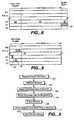
- FIG. 6shows the organization of an example one of a large number of individually addressable blocks of memory cells in a typical system.
- the block of memory cellsthe unit of erase, is divided into a number of pages P 0 through PN.
- the number N of pages in a blockcan be 8, 16 or 32, as examples.
- Each single pageis the unit of programming and reading.
- One or more host sectors of dataare stored as user data in each page. Physically, a page may be formed of a single row of memory cells within either of the arrays 1 or 11 of the systems of FIGS. 1 and 2 .
- a page P 3 of FIG. 6for example, includes space 81 for the user data and space 83 for a header of overhead data related to the user data.
- An ECC calculated from the user data stored in memory space 81is stored in the space 83 , for example.
- Some memory arraysalso include a few spare bytes of storage capacity in a space 85 to replace any bad bytes within the user space 81 .
- Block overhead data 87is shown, for example, to be part of the page P 1 .
- An important piece of information stored as part of the data 87is often a count of the number of times that the block in which the data 87 is stored has been erased. Alternatively, some other indication of the number of erase cycles experienced by the block may be stored. This data is useful for managing operation of the array.
- Other block overhead data 87 that can be usefulinclude optimal erase, programming and/or reading voltages for the block memory cells, flags to indicate the status of the block, logical and/or physical addresses of the block and any substitute block, and the like.
- the block overhead data 87provides information of the physical block itself, while the page overhead data 83 provides information of the user data stored in its same page. Although either or both of these types of overhead data may be stored in a block(s) different from the block to which they pertain, the storage locations shown in FIG. 6 are preferred for most applications.
- the user datais preferably stored in the memory cells of each page in multi-state; that is, each floating gate or other storage element of the memory cells is programmed into one of more than two states in order to store more than one bit of data in each storage element.
- the example shown in FIG. 4wherein the individual storage elements are programmed into one of four states, is conveniently implemented. This reduces the number of memory cells required to store a given amount of data. It is often preferable, however, to program the block overhead data in the group of cells 87 in binary; that is, each floating gate or other storage element of the memory cells is programmed into one of exactly two states.
- FIG. 5can be used.
- the advantagesinclude the ability to program the block overhead data in a reduced amount of time, with a reduced sensitivity to disturbs and field coupling effects, and with less disturbing effect upon the erased or programmed state of other memory cells in the same or adjacent blocks.
- binary programming of the block overhead datais preferably accomplished by the use of successive programming pulses and intervening state verifications as discussed above with respect to FIG. 3
- the time necessary to carry out a programming processcan be significantly reduced by increasing the magnitude of the starting pulse and/or by increasing the size of the steps ⁇ Vpgm.
- ⁇ Vpgmis a value of 0.2 volt for programming user data in multi-state
- a higher valuesuch as 0.4 volt
- the block overhead datacan be stored in the spare cells of any one of the pages within the example block of FIG. 6 .
- the page within each block in which the block overhead data is storedcan either be fixed or allowed to vary from block-to-block and over time. For example, if the page P 1 requires use of some of its spare cells to replace defective cells, and if there are not then enough spare cells remaining to store the block overhead data, the overhead data for that block can be stored in another page.
- the space for the block overhead dataneed not necessarily be at the end of a page or its memory cell row as illustrated in FIG. 6 but rather can be in some other location where unused memory cells exist.
- the block overhead dataneed not necessarily be stored in contiguously positioned memory cells, although it is likely easier for the memory controller if the data are stored in successive cell address locations.
- the memory arrayis of a NAND type, there can be some pages that are preferred over others for storing the block overhead data.
- the pagesare constrained to be programmed in a particular order, such as P 0 through PN, to reduce disturbing effects of programming one page on the programmed states of cells of other pages.
- the last pages PN and P(N ⁇ 1)tend to be more susceptible to disturbing influences than others of the pages. Therefore, it is preferable to store the block overhead data in some other page nearer to the beginning of the block, such as P 4 or P 5 of blocks having 16 pages total.
- a redundancy codesuch as an ECC may be calculated from the block overhead data and stored with that data in the same block. The ECC is then used to verify the data when it is read, and to provide an ability to correct a few invalid bits.
- the organization of the block overhead data 87 of FIG. 6 to include an ECCis shown in FIG. 7 . If the number of invalid bits of the stored block overhead data is in excess of what the ECC can correct, that information is useful to the controller. If the type of overhead data being stored is important to the operation of the memory system, then the inability to read that data from a block will be used by the controller to map out that block so that it is not used again. A flag may be set within the block to indicate that it is not to be used, or the controller can independently keep a list of invalid blocks.
- FIG. 8A memory cell block arrangement different from FIG. 6 is shown in FIG. 8 , in order to provide another implementation.
- spare cellsare not included in each page.
- the block overhead datatherefore, needs to be stored elsewhere within the block.
- the example shown in FIG. 8distributes this data in spare bytes within page headers of the block, such as in locations 91 , 93 and 95 of three different page headers. This then requires that all three pages be read before the block overhead data can be obtained, contrasted with needing to read only one page of a block in the example of FIG. 6 .
- a commandis issued by the controller ( 27 of FIG. 1 or 43 of FIG. 2 ) to simultaneously erase a number of one or more blocks specified by addresses issued in a step 103 .
- the controllerreads the block overhead data from each of the addressed blocks. In a usual system, this involves reading the entire page(s) of each addressed block in which their block overhead data is stored since the page is the unit of programming and erasing.
- the overhead datacan be, for example, the data 87 of FIG. 6 or the data 91 , 93 , 95 of FIG. 8 .
- the controllerreads the overhead data with a different set of reference levels than are used when reading the user data and headers. This read data is then temporarily stored in the system by the controller, most conveniently in random-access-memory (RAM) 28 or 45 that is included as part of the respective controller 27 and state machine 8 .
- RAMrandom-access-memory
- the block overhead dataare stored along with an ECC or other redundancy code calculated from the data, the validity of the data is then checked before writing it into the RAM. If determined to be valid, or if erroneous overhead data can be corrected to make it valid, the process proceeds as described. However, if the block overhead data are not, or cannot be made to be, valid, then it may be desired to take the block out of service because of a concern that the block cannot in the future be operated properly when its history is not known. The erase process may then be stopped with respect to that block and its address added to a bad block list maintained by the controller. Alternatively, the erase process may continue and a flag written into the overhead space of the block to indicate that it is no longer to be used. The controller then looks for such flags when determining the blocks to be subjected to future erase and programming cycles.
- the block overhead datawill be lost if the RAM in which the data is temporarily stored in volatile memory, which is usually the case. In this situation, the controller, once power is restored, has no block overhead data to write back into the erased blocks. Any future attempts to use the blocks that involve reading the block overhead data, when such data do not exist, can cause the controller to then map the blocks out of the system by adding their addresses to the bad block list, setting a flag in the blocks, or by some other technique.
- an important piece of block overhead datacan be the number of times the individual block has experienced an erase and re-programming cycle. This number, or some quantity related to that number, if included, is then updated as part of the erase cycle.
- the quantity stored in the controller RAMis read from RAM and updated for each block being erased to record that the block has been subjected to another erase cycle. As indicated by a step 111 of FIG. 9 , the updated number is written back into each block to which it pertains.
- the simplest implementationis to increment the erase cycle count read from the block by one, and then write that incremented count back into the block after it has been erased.
- the block overhead datamay also include other information data that is not updated each time the block is erased, in which case this type of data is written back into the erased block without any change. If an ECC or other redundancy code is used with the block overhead data, such a code is calculated from the updated overhead data to be written back into the block and then programmed along with the updated overhead data into the block.
- a last step of the erase cycleis for the array and its peripheral circuits to send a completion status signal back to the controller, as indicated in step 113 .
- the erased blocksremain erased except in the location(s) where the block overhead data are programmed. User data may thereafter be programmed into the pages of the block.
- the erase cycle countcan be used in a number of different ways. Since certain characteristics of the memory cells change as their number of erase/programming cycles increases, operation of the array is optimized if affected operating parameters are also changed. Examples of such operating parameters include erase and programming voltages, and the frequency that user data within the blocks are refreshed to bring charge levels back within optimal ranges. Blocks with low cycle counts can be operated with lower programming and erase voltages, thereby to extend their useful life. Data refreshing can affect performance if it occurs too often, so blocks with low cycle counts are not refreshed as often as those with high cycle counts. The cycle count can also be utilized to even out the usage (wear) of the individual blocks by altering a logical-to-physical block address table when differences in usage of various blocks exceeds some pre-set limits. Additionally, if any blocks experience a number of cycles that exceeds their expected useful lifetime, those blocks can be permanently mapped out of the system.
Landscapes
- Engineering & Computer Science (AREA)
- Microelectronics & Electronic Packaging (AREA)
- Computer Hardware Design (AREA)
- Theoretical Computer Science (AREA)
- Quality & Reliability (AREA)
- Physics & Mathematics (AREA)
- General Engineering & Computer Science (AREA)
- General Physics & Mathematics (AREA)
- Read Only Memory (AREA)
- Non-Volatile Memory (AREA)
- Techniques For Improving Reliability Of Storages (AREA)
Abstract
Description
Claims (20)
Priority Applications (14)
| Application Number | Priority Date | Filing Date | Title |
|---|---|---|---|
| US10/353,574US6944063B2 (en) | 2003-01-28 | 2003-01-28 | Non-volatile semiconductor memory with large erase blocks storing cycle counts |
| AU2003297327AAU2003297327A1 (en) | 2003-01-28 | 2003-12-18 | Non-volatile semiconductor memory with large erase blocks storing cycle counts |
| CN2003801092176ACN1754230B (en) | 2003-01-28 | 2003-12-18 | A method of operating non-volatile memory |
| JP2004568035AJP4648006B2 (en) | 2003-01-28 | 2003-12-18 | Nonvolatile semiconductor memory having wide erase block for storing cycle count value |
| AT03815779TATE387715T1 (en) | 2003-01-28 | 2003-12-18 | NON-VOLATILE SEMICONDUCTOR MEMORY WITH LARGE ERASE BLOCKS STORING CYCLE COUNT VALUES |
| EP03815779AEP1588379B1 (en) | 2003-01-28 | 2003-12-18 | Non-volatile semiconductor memory with large erase blocks storing cycle counts |
| KR1020057013970AKR101089575B1 (en) | 2003-01-28 | 2003-12-18 | Non-volatile semiconductor memory with large erase blocks storing cycle counts |
| EP07076027AEP1975942B1 (en) | 2003-01-28 | 2003-12-18 | Non-volatile semiconductor memory with large erase blocks storing cycle counts |
| PCT/US2003/040361WO2004070731A1 (en) | 2003-01-28 | 2003-12-18 | Non-volatile semiconductor memory with large erase blocks storing cycle counts |
| DE60319437TDE60319437T2 (en) | 2003-01-28 | 2003-12-18 | NON-VOLATILE SEMICONDUCTOR MEMORY WITH CYCLE COUNTER VALVES STORING LARGE DEFICIENCIES |
| TW093101054ATWI323466B (en) | 2003-01-28 | 2004-01-15 | Non-volatile semiconductor memory with large erase blocks storing cycle counts and method of operating the same |
| US11/003,046US7085161B2 (en) | 2003-01-28 | 2004-12-02 | Non-volatile semiconductor memory with large erase blocks storing cycle counts |
| US11/004,139US7307881B2 (en) | 2003-01-28 | 2004-12-02 | Non-volatile semiconductor memory with large erase blocks storing cycle counts |
| US11/419,696US7394692B2 (en) | 2003-01-28 | 2006-05-22 | Non-volatile semiconductor memory with large erase blocks storing cycle counts |
Applications Claiming Priority (1)
| Application Number | Priority Date | Filing Date | Title |
|---|---|---|---|
| US10/353,574US6944063B2 (en) | 2003-01-28 | 2003-01-28 | Non-volatile semiconductor memory with large erase blocks storing cycle counts |
Related Child Applications (2)
| Application Number | Title | Priority Date | Filing Date |
|---|---|---|---|
| US11/004,139DivisionUS7307881B2 (en) | 2003-01-28 | 2004-12-02 | Non-volatile semiconductor memory with large erase blocks storing cycle counts |
| US11/003,046DivisionUS7085161B2 (en) | 2003-01-28 | 2004-12-02 | Non-volatile semiconductor memory with large erase blocks storing cycle counts |
Publications (2)
| Publication Number | Publication Date |
|---|---|
| US20040145952A1 US20040145952A1 (en) | 2004-07-29 |
| US6944063B2true US6944063B2 (en) | 2005-09-13 |
Family
ID=32736208
Family Applications (4)
| Application Number | Title | Priority Date | Filing Date |
|---|---|---|---|
| US10/353,574Expired - LifetimeUS6944063B2 (en) | 2003-01-28 | 2003-01-28 | Non-volatile semiconductor memory with large erase blocks storing cycle counts |
| US11/004,139Expired - LifetimeUS7307881B2 (en) | 2003-01-28 | 2004-12-02 | Non-volatile semiconductor memory with large erase blocks storing cycle counts |
| US11/003,046Expired - LifetimeUS7085161B2 (en) | 2003-01-28 | 2004-12-02 | Non-volatile semiconductor memory with large erase blocks storing cycle counts |
| US11/419,696Expired - LifetimeUS7394692B2 (en) | 2003-01-28 | 2006-05-22 | Non-volatile semiconductor memory with large erase blocks storing cycle counts |
Family Applications After (3)
| Application Number | Title | Priority Date | Filing Date |
|---|---|---|---|
| US11/004,139Expired - LifetimeUS7307881B2 (en) | 2003-01-28 | 2004-12-02 | Non-volatile semiconductor memory with large erase blocks storing cycle counts |
| US11/003,046Expired - LifetimeUS7085161B2 (en) | 2003-01-28 | 2004-12-02 | Non-volatile semiconductor memory with large erase blocks storing cycle counts |
| US11/419,696Expired - LifetimeUS7394692B2 (en) | 2003-01-28 | 2006-05-22 | Non-volatile semiconductor memory with large erase blocks storing cycle counts |
Country Status (10)
| Country | Link |
|---|---|
| US (4) | US6944063B2 (en) |
| EP (2) | EP1588379B1 (en) |
| JP (1) | JP4648006B2 (en) |
| KR (1) | KR101089575B1 (en) |
| CN (1) | CN1754230B (en) |
| AT (1) | ATE387715T1 (en) |
| AU (1) | AU2003297327A1 (en) |
| DE (1) | DE60319437T2 (en) |
| TW (1) | TWI323466B (en) |
| WO (1) | WO2004070731A1 (en) |
Cited By (30)
| Publication number | Priority date | Publication date | Assignee | Title |
|---|---|---|---|---|
| US20030135793A1 (en)* | 2002-01-16 | 2003-07-17 | Sandisk Corporation | Method and apparatus for dynamic degradation detection |
| US20040170056A1 (en)* | 2002-11-29 | 2004-09-02 | Kabushiki Kaisha Toshiba | Semiconductor memory device for storing multivalued data |
| US20050102444A1 (en)* | 2003-11-07 | 2005-05-12 | Cruz Arnaldo R. | Memory controller useable in a data processing system |
| US20060206770A1 (en)* | 2003-01-28 | 2006-09-14 | Jian Chen | Non-Volatile Semiconductor Memory With Large Erase Blocks Storing Cycle Counts |
| US20060256623A1 (en)* | 2005-05-12 | 2006-11-16 | Micron Technology, Inc. | Partial string erase scheme in a flash memory device |
| US20060256624A1 (en)* | 2003-06-24 | 2006-11-16 | Micron Technology, Inc. | Erase block data splitting |
| US7139863B1 (en)* | 2003-09-26 | 2006-11-21 | Storage Technology Corporation | Method and system for improving usable life of memory devices using vector processing |
| US20070168840A1 (en)* | 2004-11-08 | 2007-07-19 | Micron Technology, Inc. | Memory block quality identification in a memory device |
| US20070245067A1 (en)* | 2006-04-13 | 2007-10-18 | Emilio Yero | Cycle count storage systems |
| US20070245068A1 (en)* | 2006-04-13 | 2007-10-18 | Emilio Yero | Cycle count storage methods |
| US20070260811A1 (en)* | 2006-05-08 | 2007-11-08 | Merry David E Jr | Systems and methods for measuring the useful life of solid-state storage devices |
| US20080056006A1 (en)* | 2006-08-30 | 2008-03-06 | Kee-Ho Jung | Flash memory device and method for programming multi-level cells in the same |
| US20080055998A1 (en)* | 2006-08-30 | 2008-03-06 | Samsung Electronics Co., Ltd. | Flash memory device and method for programming multi-level cells in the same |
| US20080077840A1 (en)* | 2006-09-27 | 2008-03-27 | Mark Shaw | Memory system and method for storing and correcting data |
| US20080147962A1 (en)* | 2006-12-15 | 2008-06-19 | Diggs Mark S | Storage subsystem with multiple non-volatile memory arrays to protect against data losses |
| US20080189452A1 (en)* | 2007-02-07 | 2008-08-07 | Merry David E | Storage subsystem with configurable buffer |
| US7495966B2 (en) | 2006-05-01 | 2009-02-24 | Micron Technology, Inc. | Memory voltage cycle adjustment |
| US7523380B1 (en)* | 2003-12-16 | 2009-04-21 | Xilinx, Inc. | Methods and structures for providing programmable width and error correction in memory arrays in programmable logic devices |
| US20090204853A1 (en)* | 2008-02-11 | 2009-08-13 | Siliconsystems, Inc. | Interface for enabling a host computer to retrieve device monitor data from a solid state storage subsystem |
| US20090204852A1 (en)* | 2008-02-07 | 2009-08-13 | Siliconsystems, Inc. | Solid state storage subsystem that maintains and provides access to data reflective of a failure risk |
| US20090296472A1 (en)* | 2004-12-21 | 2009-12-03 | Samsung Electronics Co., Ltd. | Flash memory devices and methods of programming the same by overlapping programming operations for multiple mats |
| US20100162084A1 (en)* | 2008-12-18 | 2010-06-24 | Richard Coulson | Data error recovery in non-volatile memory |
| US20100174847A1 (en)* | 2009-01-05 | 2010-07-08 | Alexander Paley | Non-Volatile Memory and Method With Write Cache Partition Management Methods |
| US20100172179A1 (en)* | 2009-01-05 | 2010-07-08 | Sergey Anatolievich Gorobets | Spare Block Management of Non-Volatile Memories |
| US8094500B2 (en) | 2009-01-05 | 2012-01-10 | Sandisk Technologies Inc. | Non-volatile memory and method with write cache partitioning |
| US8700840B2 (en) | 2009-01-05 | 2014-04-15 | SanDisk Technologies, Inc. | Nonvolatile memory with write cache having flush/eviction methods |
| US8799747B2 (en) | 2010-06-03 | 2014-08-05 | Seagate Technology Llc | Data hardening to compensate for loss of data retention characteristics in a non-volatile memory |
| US9190142B2 (en) | 2014-03-12 | 2015-11-17 | Kabushiki Kaisha Toshiba | Semiconductor memory device and method of controlling the same |
| US10978156B2 (en) | 2018-06-29 | 2021-04-13 | Sandisk Technologies Llc | Concurrent programming of multiple cells for non-volatile memory devices |
| US11545221B2 (en) | 2018-06-29 | 2023-01-03 | Sandisk Technologies Llc | Concurrent programming of multiple cells for non-volatile memory devices |
Families Citing this family (73)
| Publication number | Priority date | Publication date | Assignee | Title |
|---|---|---|---|---|
| JP4230753B2 (en)* | 2002-10-30 | 2009-02-25 | 株式会社東芝 | Semiconductor memory |
| US7259989B2 (en)* | 2004-09-03 | 2007-08-21 | Matsushita Electric Industrial Co., Ltd. | Non-volatile memory device |
| JP4660316B2 (en)* | 2004-09-03 | 2011-03-30 | パナソニック株式会社 | Nonvolatile memory device |
| CN101001629B (en) | 2004-09-17 | 2010-05-05 | 卫材R&D管理有限公司 | Pharmaceutical composition |
| US7412560B2 (en)* | 2004-12-16 | 2008-08-12 | Sandisk Corporation | Non-volatile memory and method with multi-stream updating |
| KR100672121B1 (en) | 2005-01-12 | 2007-01-19 | 주식회사 하이닉스반도체 | Nonvolatile Memory Device and Its Program / Reading Method |
| JP4575288B2 (en)* | 2005-12-05 | 2010-11-04 | 株式会社東芝 | Storage medium, storage medium playback apparatus, storage medium playback method, and storage medium playback program |
| KR100703806B1 (en)* | 2006-02-16 | 2007-04-09 | 삼성전자주식회사 | Non-volatile memory, apparatus and method for determining data validity therefor |
| JP2008009527A (en)* | 2006-06-27 | 2008-01-17 | Toshiba Corp | Memory system |
| KR100736103B1 (en)* | 2006-06-27 | 2007-07-06 | 삼성전자주식회사 | Non-volatile memory, apparatus and method for determining data validity of the non-volatile memory |
| JP5002201B2 (en)* | 2006-06-30 | 2012-08-15 | 株式会社東芝 | Memory system |
| US7529969B1 (en)* | 2006-08-24 | 2009-05-05 | Micron Technology, Inc. | Memory device internal parameter reliability |
| KR100805840B1 (en)* | 2006-09-01 | 2008-02-21 | 삼성전자주식회사 | Flash Memory Device Using Cache and Its Program Method |
| KR100908526B1 (en)* | 2006-09-29 | 2009-07-20 | 주식회사 하이닉스반도체 | Flash memory device and erase method thereof |
| TW200828320A (en) | 2006-12-28 | 2008-07-01 | Genesys Logic Inc | Method for performing static wear leveling on flash memory |
| US7877665B2 (en)* | 2006-12-29 | 2011-01-25 | Sandisk Corporation | Page by page ECC variation in a memory device |
| US7870457B2 (en)* | 2006-12-29 | 2011-01-11 | Sandisk Corporation | Page by page ECC variation in a memory device |
| WO2008083161A1 (en)* | 2006-12-29 | 2008-07-10 | Sandisk Corporation | Page by page ecc variation in a memory device |
| US7925151B2 (en)* | 2007-01-31 | 2011-04-12 | Kobre Kenneth R | Device for redirecting and reflecting light from camera flash and methods for using same |
| US7958301B2 (en)* | 2007-04-10 | 2011-06-07 | Marvell World Trade Ltd. | Memory controller and method for memory pages with dynamically configurable bits per cell |
| KR100866626B1 (en)* | 2007-07-02 | 2008-11-03 | 삼성전자주식회사 | Nonvolatile memory device having spare area and block erasing method thereof |
| KR101397549B1 (en)* | 2007-08-16 | 2014-05-26 | 삼성전자주식회사 | Non-volatile semiconductor memory device and system capable of fast rogramming and read method thereof |
| CN101383186B (en)* | 2007-09-05 | 2011-09-14 | 联咏科技股份有限公司 | Programming method and device and reading method of NAND gate flash memory |
| US20090080258A1 (en)* | 2007-09-21 | 2009-03-26 | Walker Andrew J | Erase method in thin film nonvolatile memory |
| US7894263B2 (en)* | 2007-09-28 | 2011-02-22 | Sandisk Corporation | High voltage generation and control in source-side injection programming of non-volatile memory |
| US8045373B2 (en)* | 2007-10-02 | 2011-10-25 | Cypress Semiconductor Corporation | Method and apparatus for programming memory cell array |
| NZ562200A (en)* | 2007-10-04 | 2008-11-28 | Arc Innovations Ltd | Method and system for updating a stored data value in a non-volatile memory |
| EP2215636B1 (en)* | 2007-11-26 | 2014-07-23 | Hyperstone GmbH | Method for even utilization of a plurality of flash memory chips |
| US7925822B2 (en)* | 2008-01-31 | 2011-04-12 | Sandisk Il Ltd | Erase count recovery |
| JP5214422B2 (en)* | 2008-02-15 | 2013-06-19 | 株式会社東芝 | Data storage system |
| EP2308058B1 (en)* | 2008-07-01 | 2016-01-27 | LSI Corporation | Methods and apparatus for read-side intercell interference mitigation in flash memories |
| TWI364661B (en)* | 2008-09-25 | 2012-05-21 | Silicon Motion Inc | Access methods for a flash memory and memory devices |
| CN102855943B (en)* | 2008-11-28 | 2017-04-12 | 群联电子股份有限公司 | Error correction controller, flash memory chip system thereof and error correction method |
| US8825940B1 (en) | 2008-12-02 | 2014-09-02 | Siliconsystems, Inc. | Architecture for optimizing execution of storage access commands |
| US9176859B2 (en)* | 2009-01-07 | 2015-11-03 | Siliconsystems, Inc. | Systems and methods for improving the performance of non-volatile memory operations |
| KR101038991B1 (en)* | 2009-03-10 | 2011-06-03 | 주식회사 하이닉스반도체 | Semiconductor storage system and its control method for even use of memory area |
| US10079048B2 (en)* | 2009-03-24 | 2018-09-18 | Western Digital Technologies, Inc. | Adjusting access of non-volatile semiconductor memory based on access time |
| KR101586047B1 (en)* | 2009-03-25 | 2016-01-18 | 삼성전자주식회사 | Nonvolatile memory device and its programming method |
| TWI404071B (en)* | 2009-06-23 | 2013-08-01 | Phison Electronics Corp | Controller circuit having functions for identifying error data in flash memory and storage system and method thereof |
| JP2010055745A (en)* | 2009-12-07 | 2010-03-11 | Toshiba Corp | Storage medium |
| CN102543198B (en)* | 2010-12-20 | 2015-11-25 | 北京兆易创新科技股份有限公司 | A kind of programmed method of MLC memory cell and device |
| KR20120096212A (en)* | 2011-02-22 | 2012-08-30 | 삼성전자주식회사 | Non-volatile memory device, memory controller, and methods thereof |
| KR20120128014A (en) | 2011-05-16 | 2012-11-26 | 삼성전자주식회사 | Operating method of nonvolatile memory device and operating method of memory system including nonvolatile memory device |
| KR20120128978A (en)* | 2011-05-18 | 2012-11-28 | 삼성전자주식회사 | Data storage device and data management method thereof |
| US8902653B2 (en) | 2011-08-12 | 2014-12-02 | Micron Technology, Inc. | Memory devices and configuration methods for a memory device |
| KR20130033017A (en)* | 2011-09-26 | 2013-04-03 | 에스케이하이닉스 주식회사 | Operating method for nonvolatile memory device |
| JP5781047B2 (en)* | 2012-10-17 | 2015-09-16 | 株式会社東芝 | Storage media |
| US10127150B2 (en) | 2012-11-09 | 2018-11-13 | Sandisk Technologies Llc | Key value addressed storage drive using NAND flash based content addressable memory |
| JP2013137792A (en)* | 2013-02-28 | 2013-07-11 | Toshiba Corp | Electronic device and method for controlling the same |
| US9075424B2 (en) | 2013-03-06 | 2015-07-07 | Sandisk Technologies Inc. | Compensation scheme to improve the stability of the operational amplifiers |
| US8908441B1 (en)* | 2013-10-15 | 2014-12-09 | Sandisk Technologies Inc. | Double verify method in multi-pass programming to suppress read noise |
| TWI515737B (en)* | 2013-12-09 | 2016-01-01 | 慧榮科技股份有限公司 | Data storage device and data erasing method |
| US20150169438A1 (en)* | 2013-12-18 | 2015-06-18 | Infineon Technologies Ag | Method and device for incrementing an erase counter |
| US9230689B2 (en)* | 2014-03-17 | 2016-01-05 | Sandisk Technologies Inc. | Finding read disturbs on non-volatile memories |
| US9811458B2 (en) | 2014-03-19 | 2017-11-07 | Htc Corporation | Mobile electronic device and method for clearing memory blocks based on processor determination of physical block to erase in response to GUI input from user specified time and directing controller to erase within the specified time |
| CN104932981B (en)* | 2014-03-20 | 2018-05-25 | 宏达国际电子股份有限公司 | Mobile electronic device and method for cleaning memory block |
| US9607703B2 (en) | 2014-09-08 | 2017-03-28 | Kabushiki Kaisha Toshiba | Memory system |
| US9305638B1 (en)* | 2014-10-29 | 2016-04-05 | Macronix International Co., Ltd. | Operation method for memory device |
| US9852799B2 (en) | 2014-11-19 | 2017-12-26 | Sandisk Technologies Llc | Configuration parameter management for non-volatile data storage |
| US10643700B2 (en)* | 2015-10-29 | 2020-05-05 | Micron Technology, Inc. | Apparatuses and methods for adjusting write parameters based on a write count |
| FR3044818B1 (en) | 2015-12-02 | 2018-03-30 | Stmicroelectronics (Rousset) Sas | METHOD FOR MANAGING A DEFECTIVE LINE OF THE MEMORY PLAN OF A NON-VOLATILE MEMORY AND CORRESPONDING MEMORY DEVICE |
| TWI604455B (en)* | 2016-05-13 | 2017-11-01 | Silicon Motion Inc | Data management method and data block management method for data storage device and memory controller |
| KR102730871B1 (en)* | 2016-09-19 | 2024-11-19 | 에스케이하이닉스 주식회사 | Memory system and operating method of memory system |
| CN109935264B (en)* | 2017-12-18 | 2021-03-26 | 北京兆易创新科技股份有限公司 | Memory unit erasing method and device and memory |
| KR102658230B1 (en)* | 2018-06-01 | 2024-04-17 | 삼성전자주식회사 | Semiconductor memory devices, memory systems including the same and method of operating semiconductor memory devices |
| KR102387960B1 (en)* | 2018-07-23 | 2022-04-19 | 삼성전자주식회사 | Controller and method of operating the same |
| US10891077B2 (en)* | 2018-12-26 | 2021-01-12 | Macronix International Co., Ltd. | Flash memory device and controlling method thereof |
| JP2020144554A (en)* | 2019-03-05 | 2020-09-10 | キオクシア株式会社 | Storage device and data reading method |
| JP6727365B1 (en)* | 2019-03-27 | 2020-07-22 | ウィンボンド エレクトロニクス コーポレーション | Semiconductor memory device |
| CN110865772A (en)* | 2019-11-11 | 2020-03-06 | 深圳忆联信息系统有限公司 | Method and device for protecting system data physical block erasure count value, computer equipment and storage medium |
| US11435914B2 (en)* | 2020-03-30 | 2022-09-06 | Western Digital Technologies, Inc. | Dynamic ZNS open zone active limit |
| KR102821742B1 (en)* | 2020-06-09 | 2025-06-18 | 에스케이하이닉스 주식회사 | Storage device and operating method thereof |
| CN114005476A (en)* | 2021-10-29 | 2022-02-01 | 锐凌无线通讯科技(深圳)有限公司 | Flash memory, flash memory erasing and writing counting method, electronic equipment and computer storage medium |
Citations (49)
| Publication number | Priority date | Publication date | Assignee | Title |
|---|---|---|---|---|
| US4622656A (en) | 1982-12-16 | 1986-11-11 | Seiko Instruments & Electronics Ltd. | Non-volatile semiconductor memory |
| US5043940A (en) | 1988-06-08 | 1991-08-27 | Eliyahou Harari | Flash EEPROM memory systems having multistate storage cells |
| US5070032A (en) | 1989-03-15 | 1991-12-03 | Sundisk Corporation | Method of making dense flash eeprom semiconductor memory structures |
| US5095344A (en) | 1988-06-08 | 1992-03-10 | Eliyahou Harari | Highly compact eprom and flash eeprom devices |
| US5172338A (en) | 1989-04-13 | 1992-12-15 | Sundisk Corporation | Multi-state EEprom read and write circuits and techniques |
| US5268870A (en) | 1988-06-08 | 1993-12-07 | Eliyahou Harari | Flash EEPROM system and intelligent programming and erasing methods therefor |
| US5297148A (en) | 1989-04-13 | 1994-03-22 | Sundisk Corporation | Flash eeprom system |
| EP0589597A2 (en) | 1992-09-22 | 1994-03-30 | International Business Machines Corporation | Flash non-volatile memory |
| US5313421A (en) | 1992-01-14 | 1994-05-17 | Sundisk Corporation | EEPROM with split gate source side injection |
| US5315541A (en) | 1992-07-24 | 1994-05-24 | Sundisk Corporation | Segmented column memory array |
| US5343063A (en) | 1990-12-18 | 1994-08-30 | Sundisk Corporation | Dense vertical programmable read only memory cell structure and processes for making them |
| US5438573A (en) | 1991-09-13 | 1995-08-01 | Sundisk Corporation | Flash EEPROM array data and header file structure |
| US5485595A (en) | 1993-03-26 | 1996-01-16 | Cirrus Logic, Inc. | Flash memory mass storage architecture incorporating wear leveling technique without using cam cells |
| US5570315A (en) | 1993-09-21 | 1996-10-29 | Kabushiki Kaisha Toshiba | Multi-state EEPROM having write-verify control circuit |
| US5661053A (en) | 1994-05-25 | 1997-08-26 | Sandisk Corporation | Method of making dense flash EEPROM cell array and peripheral supporting circuits formed in deposited field oxide with the use of spacers |
| US5712180A (en) | 1992-01-14 | 1998-01-27 | Sundisk Corporation | EEPROM with split gate source side injection |
| US5774397A (en) | 1993-06-29 | 1998-06-30 | Kabushiki Kaisha Toshiba | Non-volatile semiconductor memory device and method of programming a non-volatile memory cell to a predetermined state |
| US5822251A (en)* | 1997-08-25 | 1998-10-13 | Bit Microsystems, Inc. | Expandable flash-memory mass-storage using shared buddy lines and intermediate flash-bus between device-specific buffers and flash-intelligent DMA controllers |
| US5835935A (en) | 1995-09-13 | 1998-11-10 | Lexar Media, Inc. | Method of and architecture for controlling system data with automatic wear leveling in a semiconductor non-volatile mass storage memory |
| US5851881A (en) | 1997-10-06 | 1998-12-22 | Taiwan Semiconductor Manufacturing Company, Ltd. | Method of making monos flash memory for multi-level logic |
| US5860124A (en)* | 1996-09-30 | 1999-01-12 | Intel Corporation | Method for performing a continuous over-write of a file in nonvolatile memory |
| US5887145A (en) | 1993-09-01 | 1999-03-23 | Sandisk Corporation | Removable mother/daughter peripheral card |
| US5930167A (en) | 1997-07-30 | 1999-07-27 | Sandisk Corporation | Multi-state non-volatile flash memory capable of being its own two state write cache |
| US5928370A (en) | 1997-02-05 | 1999-07-27 | Lexar Media, Inc. | Method and apparatus for verifying erasure of memory blocks within a non-volatile memory structure |
| US5930815A (en)* | 1995-07-31 | 1999-07-27 | Lexar Media, Inc. | Moving sequential sectors within a block of information in a flash memory mass storage architecture |
| US6028794A (en) | 1997-01-17 | 2000-02-22 | Kabushiki Kaisha Toshiba | Nonvolatile semiconductor memory device and erasing method of the same |
| US6046935A (en) | 1996-03-18 | 2000-04-04 | Kabushiki Kaisha Toshiba | Semiconductor device and memory system |
| US6076137A (en) | 1997-12-11 | 2000-06-13 | Lexar Media, Inc. | Method and apparatus for storing location identification information within non-volatile memory devices |
| US6081447A (en) | 1991-09-13 | 2000-06-27 | Western Digital Corporation | Wear leveling techniques for flash EEPROM systems |
| US6103573A (en) | 1999-06-30 | 2000-08-15 | Sandisk Corporation | Processing techniques for making a dual floating gate EEPROM cell array |
| US6128695A (en) | 1995-07-31 | 2000-10-03 | Lexar Media, Inc. | Identification and verification of a sector within a block of mass storage flash memory |
| US6134143A (en)* | 1997-12-01 | 2000-10-17 | Micron Technology, Inc. | Multi-state flash memory defect management |
| US6151248A (en) | 1999-06-30 | 2000-11-21 | Sandisk Corporation | Dual floating gate EEPROM cell array with steering gates shared by adjacent cells |
| US6202138B1 (en)* | 1995-07-31 | 2001-03-13 | Lexar Media, Inc | Increasing the memory performance of flash memory devices by writing sectors simultaneously to multiple flash memory devices |
| US6222762B1 (en) | 1992-01-14 | 2001-04-24 | Sandisk Corporation | Multi-state memory |
| US6281075B1 (en) | 1999-01-27 | 2001-08-28 | Sandisk Corporation | Method of controlling of floating gate oxide growth by use of an oxygen barrier |
| WO2002058074A2 (en) | 2001-01-19 | 2002-07-25 | Sandisk Corporation | Partial block data programming and reading operations in a non-volatile memory |
| US6426893B1 (en) | 2000-02-17 | 2002-07-30 | Sandisk Corporation | Flash eeprom system with simultaneous multiple data sector programming and storage of physical block characteristics in other designated blocks |
| US6456528B1 (en) | 2001-09-17 | 2002-09-24 | Sandisk Corporation | Selective operation of a multi-state non-volatile memory system in a binary mode |
| US20020172227A1 (en)* | 2001-05-21 | 2002-11-21 | Varelas Oreste B. | Method and apparatus for frame-based protocol processing |
| US6512263B1 (en) | 2000-09-22 | 2003-01-28 | Sandisk Corporation | Non-volatile memory cell array having discontinuous source and drain diffusions contacted by continuous bit line conductors and methods of forming |
| US6522580B2 (en) | 2001-06-27 | 2003-02-18 | Sandisk Corporation | Operating techniques for reducing effects of coupling between storage elements of a non-volatile memory operated in multiple data states |
| US20030041210A1 (en)* | 2001-08-24 | 2003-02-27 | Micron Technology, Inc. | Erase block management |
| US6684289B1 (en)* | 2000-11-22 | 2004-01-27 | Sandisk Corporation | Techniques for operating non-volatile memory systems with data sectors having different sizes than the sizes of the pages and/or blocks of the memory |
| US20040047182A1 (en)* | 2002-09-06 | 2004-03-11 | Raul-Adrian Cernea | Techniques for reducing effects of coupling between storage elements of adjacent rows of memory cells |
| US6721843B1 (en)* | 2000-07-07 | 2004-04-13 | Lexar Media, Inc. | Flash memory architecture implementing simultaneously programmable multiple flash memory banks that are host compatible |
| US20040083405A1 (en)* | 2002-10-28 | 2004-04-29 | Sandisk Corporation | Power management block for use in a non-volatile memory system |
| US20040080995A1 (en)* | 2000-09-14 | 2004-04-29 | Nima Mokhlesi | Compressed event counting technique and application to a flash memory system |
| US6829167B2 (en)* | 2002-12-12 | 2004-12-07 | Sandisk Corporation | Error recovery for nonvolatile memory |
Family Cites Families (30)
| Publication number | Priority date | Publication date | Assignee | Title |
|---|---|---|---|---|
| US568870A (en)* | 1896-10-06 | Mark m | ||
| US5844842A (en)* | 1989-02-06 | 1998-12-01 | Hitachi, Ltd. | Nonvolatile semiconductor memory device |
| US5291440A (en)* | 1990-07-30 | 1994-03-01 | Nec Corporation | Non-volatile programmable read only memory device having a plurality of memory cells each implemented by a memory transistor and a switching transistor stacked thereon |
| US5281075A (en)* | 1991-11-15 | 1994-01-25 | Tatman Darrell J | Apparatus for transporting recreational type vehicles |
| US5443063A (en)* | 1993-08-31 | 1995-08-22 | The Johns Hopkins University | Cuffed oro-pharyngeal airway |
| JP3153730B2 (en)* | 1995-05-16 | 2001-04-09 | 株式会社東芝 | Nonvolatile semiconductor memory device |
| KR100253868B1 (en)* | 1995-11-13 | 2000-05-01 | 니시무로 타이죠 | Non-volatile semiconductor memory device |
| US5619448A (en)* | 1996-03-14 | 1997-04-08 | Myson Technology, Inc. | Non-volatile memory device and apparatus for reading a non-volatile memory array |
| JPH09330598A (en)* | 1996-06-10 | 1997-12-22 | Mitsubishi Electric Corp | Storage device and its characteristic deterioration state determination method |
| US6335878B1 (en)* | 1998-07-28 | 2002-01-01 | Hitachi, Ltd. | Non-volatile multi-level semiconductor flash memory device and method of driving same |
| JP3930074B2 (en)* | 1996-09-30 | 2007-06-13 | 株式会社ルネサステクノロジ | Semiconductor integrated circuit and data processing system |
| US5956473A (en)* | 1996-11-25 | 1999-09-21 | Macronix International Co., Ltd. | Method and system for managing a flash memory mass storage system |
| JP3946849B2 (en)* | 1997-01-17 | 2007-07-18 | 株式会社東芝 | Nonvolatile semiconductor memory device and erase method thereof |
| JPH10320984A (en) | 1997-05-15 | 1998-12-04 | Sharp Corp | Storage device |
| JP3788205B2 (en) | 1997-09-30 | 2006-06-21 | ソニー株式会社 | Storage device, data processing system, data writing and reading method, and data processing device |
| JPH11224491A (en)* | 1997-12-03 | 1999-08-17 | Sony Corp | Non-volatile semiconductor memory and ic memory card using it |
| US6614070B1 (en)* | 1998-04-16 | 2003-09-02 | Cypress Semiconductor Corporation | Semiconductor non-volatile memory device having a NAND cell structure |
| JPH11328990A (en)* | 1998-05-15 | 1999-11-30 | Hitachi Ltd | Semiconductor integrated circuit device and memory card using the same |
| US6567302B2 (en)* | 1998-12-29 | 2003-05-20 | Micron Technology, Inc. | Method and apparatus for programming multi-state cells in a memory device |
| JP2000285688A (en)* | 1999-04-01 | 2000-10-13 | Mitsubishi Electric Corp | Nonvolatile semiconductor memory device |
| US7113432B2 (en)* | 2000-09-14 | 2006-09-26 | Sandisk Corporation | Compressed event counting technique and application to a flash memory system |
| JP2001188713A (en)* | 2000-11-15 | 2001-07-10 | Fujitsu Ltd | Storage device management method |
| JP2002197878A (en)* | 2000-12-26 | 2002-07-12 | Hitachi Ltd | Semiconductor device and data processing system |
| US6738289B2 (en) | 2001-02-26 | 2004-05-18 | Sandisk Corporation | Non-volatile memory with improved programming and method therefor |
| JP4282248B2 (en)* | 2001-03-30 | 2009-06-17 | 株式会社東芝 | Semiconductor memory device |
| US6762092B2 (en) | 2001-08-08 | 2004-07-13 | Sandisk Corporation | Scalable self-aligned dual floating gate memory cell array and methods of forming the array |
| GB0123416D0 (en)* | 2001-09-28 | 2001-11-21 | Memquest Ltd | Non-volatile memory control |
| US6925007B2 (en) | 2001-10-31 | 2005-08-02 | Sandisk Corporation | Multi-state non-volatile integrated circuit memory systems that employ dielectric storage elements |
| US6967872B2 (en)* | 2001-12-18 | 2005-11-22 | Sandisk Corporation | Method and system for programming and inhibiting multi-level, non-volatile memory cells |
| US6944063B2 (en)* | 2003-01-28 | 2005-09-13 | Sandisk Corporation | Non-volatile semiconductor memory with large erase blocks storing cycle counts |
- 2003
- 2003-01-28USUS10/353,574patent/US6944063B2/ennot_activeExpired - Lifetime
- 2003-12-18EPEP03815779Apatent/EP1588379B1/ennot_activeExpired - Lifetime
- 2003-12-18ATAT03815779Tpatent/ATE387715T1/ennot_activeIP Right Cessation
- 2003-12-18CNCN2003801092176Apatent/CN1754230B/ennot_activeExpired - Lifetime
- 2003-12-18DEDE60319437Tpatent/DE60319437T2/ennot_activeExpired - Lifetime
- 2003-12-18KRKR1020057013970Apatent/KR101089575B1/ennot_activeExpired - Fee Related
- 2003-12-18JPJP2004568035Apatent/JP4648006B2/ennot_activeExpired - Fee Related
- 2003-12-18EPEP07076027Apatent/EP1975942B1/ennot_activeExpired - Lifetime
- 2003-12-18WOPCT/US2003/040361patent/WO2004070731A1/enactiveIP Right Grant
- 2003-12-18AUAU2003297327Apatent/AU2003297327A1/ennot_activeAbandoned
- 2004
- 2004-01-15TWTW093101054Apatent/TWI323466B/ennot_activeIP Right Cessation
- 2004-12-02USUS11/004,139patent/US7307881B2/ennot_activeExpired - Lifetime
- 2004-12-02USUS11/003,046patent/US7085161B2/ennot_activeExpired - Lifetime
- 2006
- 2006-05-22USUS11/419,696patent/US7394692B2/ennot_activeExpired - Lifetime
Patent Citations (53)
| Publication number | Priority date | Publication date | Assignee | Title |
|---|---|---|---|---|
| US4622656A (en) | 1982-12-16 | 1986-11-11 | Seiko Instruments & Electronics Ltd. | Non-volatile semiconductor memory |
| US5043940A (en) | 1988-06-08 | 1991-08-27 | Eliyahou Harari | Flash EEPROM memory systems having multistate storage cells |
| US5095344A (en) | 1988-06-08 | 1992-03-10 | Eliyahou Harari | Highly compact eprom and flash eeprom devices |
| US5268870A (en) | 1988-06-08 | 1993-12-07 | Eliyahou Harari | Flash EEPROM system and intelligent programming and erasing methods therefor |
| US5070032A (en) | 1989-03-15 | 1991-12-03 | Sundisk Corporation | Method of making dense flash eeprom semiconductor memory structures |
| US5172338A (en) | 1989-04-13 | 1992-12-15 | Sundisk Corporation | Multi-state EEprom read and write circuits and techniques |
| US5297148A (en) | 1989-04-13 | 1994-03-22 | Sundisk Corporation | Flash eeprom system |
| US6149316A (en)* | 1989-04-13 | 2000-11-21 | Sandisk Corporation | Flash EEprom system |
| US5172338B1 (en) | 1989-04-13 | 1997-07-08 | Sandisk Corp | Multi-state eeprom read and write circuits and techniques |
| US5343063A (en) | 1990-12-18 | 1994-08-30 | Sundisk Corporation | Dense vertical programmable read only memory cell structure and processes for making them |
| US6230233B1 (en) | 1991-09-13 | 2001-05-08 | Sandisk Corporation | Wear leveling techniques for flash EEPROM systems |
| US5438573A (en) | 1991-09-13 | 1995-08-01 | Sundisk Corporation | Flash EEPROM array data and header file structure |
| US6081447A (en) | 1991-09-13 | 2000-06-27 | Western Digital Corporation | Wear leveling techniques for flash EEPROM systems |
| US5712180A (en) | 1992-01-14 | 1998-01-27 | Sundisk Corporation | EEPROM with split gate source side injection |
| US5313421A (en) | 1992-01-14 | 1994-05-17 | Sundisk Corporation | EEPROM with split gate source side injection |
| US6222762B1 (en) | 1992-01-14 | 2001-04-24 | Sandisk Corporation | Multi-state memory |
| US5315541A (en) | 1992-07-24 | 1994-05-24 | Sundisk Corporation | Segmented column memory array |
| EP0589597A2 (en) | 1992-09-22 | 1994-03-30 | International Business Machines Corporation | Flash non-volatile memory |
| US5485595A (en) | 1993-03-26 | 1996-01-16 | Cirrus Logic, Inc. | Flash memory mass storage architecture incorporating wear leveling technique without using cam cells |
| US5774397A (en) | 1993-06-29 | 1998-06-30 | Kabushiki Kaisha Toshiba | Non-volatile semiconductor memory device and method of programming a non-volatile memory cell to a predetermined state |
| US5887145A (en) | 1993-09-01 | 1999-03-23 | Sandisk Corporation | Removable mother/daughter peripheral card |
| US5570315A (en) | 1993-09-21 | 1996-10-29 | Kabushiki Kaisha Toshiba | Multi-state EEPROM having write-verify control circuit |
| US5661053A (en) | 1994-05-25 | 1997-08-26 | Sandisk Corporation | Method of making dense flash EEPROM cell array and peripheral supporting circuits formed in deposited field oxide with the use of spacers |
| US6202138B1 (en)* | 1995-07-31 | 2001-03-13 | Lexar Media, Inc | Increasing the memory performance of flash memory devices by writing sectors simultaneously to multiple flash memory devices |
| US6128695A (en) | 1995-07-31 | 2000-10-03 | Lexar Media, Inc. | Identification and verification of a sector within a block of mass storage flash memory |
| US5930815A (en)* | 1995-07-31 | 1999-07-27 | Lexar Media, Inc. | Moving sequential sectors within a block of information in a flash memory mass storage architecture |
| US5835935A (en) | 1995-09-13 | 1998-11-10 | Lexar Media, Inc. | Method of and architecture for controlling system data with automatic wear leveling in a semiconductor non-volatile mass storage memory |
| US6046935A (en) | 1996-03-18 | 2000-04-04 | Kabushiki Kaisha Toshiba | Semiconductor device and memory system |
| US5860124A (en)* | 1996-09-30 | 1999-01-12 | Intel Corporation | Method for performing a continuous over-write of a file in nonvolatile memory |
| US6028794A (en) | 1997-01-17 | 2000-02-22 | Kabushiki Kaisha Toshiba | Nonvolatile semiconductor memory device and erasing method of the same |
| US5928370A (en) | 1997-02-05 | 1999-07-27 | Lexar Media, Inc. | Method and apparatus for verifying erasure of memory blocks within a non-volatile memory structure |
| US5930167A (en) | 1997-07-30 | 1999-07-27 | Sandisk Corporation | Multi-state non-volatile flash memory capable of being its own two state write cache |
| US5822251A (en)* | 1997-08-25 | 1998-10-13 | Bit Microsystems, Inc. | Expandable flash-memory mass-storage using shared buddy lines and intermediate flash-bus between device-specific buffers and flash-intelligent DMA controllers |
| US5851881A (en) | 1997-10-06 | 1998-12-22 | Taiwan Semiconductor Manufacturing Company, Ltd. | Method of making monos flash memory for multi-level logic |
| US6134143A (en)* | 1997-12-01 | 2000-10-17 | Micron Technology, Inc. | Multi-state flash memory defect management |
| US6076137A (en) | 1997-12-11 | 2000-06-13 | Lexar Media, Inc. | Method and apparatus for storing location identification information within non-volatile memory devices |
| US6281075B1 (en) | 1999-01-27 | 2001-08-28 | Sandisk Corporation | Method of controlling of floating gate oxide growth by use of an oxygen barrier |
| US6103573A (en) | 1999-06-30 | 2000-08-15 | Sandisk Corporation | Processing techniques for making a dual floating gate EEPROM cell array |
| US6151248A (en) | 1999-06-30 | 2000-11-21 | Sandisk Corporation | Dual floating gate EEPROM cell array with steering gates shared by adjacent cells |
| US6426893B1 (en) | 2000-02-17 | 2002-07-30 | Sandisk Corporation | Flash eeprom system with simultaneous multiple data sector programming and storage of physical block characteristics in other designated blocks |
| US6721843B1 (en)* | 2000-07-07 | 2004-04-13 | Lexar Media, Inc. | Flash memory architecture implementing simultaneously programmable multiple flash memory banks that are host compatible |
| US20040080995A1 (en)* | 2000-09-14 | 2004-04-29 | Nima Mokhlesi | Compressed event counting technique and application to a flash memory system |
| US6512263B1 (en) | 2000-09-22 | 2003-01-28 | Sandisk Corporation | Non-volatile memory cell array having discontinuous source and drain diffusions contacted by continuous bit line conductors and methods of forming |
| US6684289B1 (en)* | 2000-11-22 | 2004-01-27 | Sandisk Corporation | Techniques for operating non-volatile memory systems with data sectors having different sizes than the sizes of the pages and/or blocks of the memory |
| WO2002058074A2 (en) | 2001-01-19 | 2002-07-25 | Sandisk Corporation | Partial block data programming and reading operations in a non-volatile memory |
| US20020172227A1 (en)* | 2001-05-21 | 2002-11-21 | Varelas Oreste B. | Method and apparatus for frame-based protocol processing |
| US6522580B2 (en) | 2001-06-27 | 2003-02-18 | Sandisk Corporation | Operating techniques for reducing effects of coupling between storage elements of a non-volatile memory operated in multiple data states |
| US20030041210A1 (en)* | 2001-08-24 | 2003-02-27 | Micron Technology, Inc. | Erase block management |
| US6456528B1 (en) | 2001-09-17 | 2002-09-24 | Sandisk Corporation | Selective operation of a multi-state non-volatile memory system in a binary mode |
| US20040047182A1 (en)* | 2002-09-06 | 2004-03-11 | Raul-Adrian Cernea | Techniques for reducing effects of coupling between storage elements of adjacent rows of memory cells |
| US20050018482A1 (en)* | 2002-09-06 | 2005-01-27 | Raul-Adrian Cemea | Techniques for reducing effects of coupling between storage elements of adjacent rows of memory cells |
| US20040083405A1 (en)* | 2002-10-28 | 2004-04-29 | Sandisk Corporation | Power management block for use in a non-volatile memory system |
| US6829167B2 (en)* | 2002-12-12 | 2004-12-07 | Sandisk Corporation | Error recovery for nonvolatile memory |
Non-Patent Citations (6)
| Title |
|---|
| "Notification of Transmittal of the International Search Report or the Declaration", corresponding PCT application no. PCT/US03/40361, International Searching Authority, European Patent Office, Jan. 6, 2004, 7 pages. |
| Brown et al., "Nonvolatile Semiconductor Memory Technology," IEEE Press, Section 1.2, 1998, pp. 9-25. |
| Chan et al., "A True Single-Transistor Oxide-Nitiride-Oxide EEPROM Device," IEEE Electron Device Letters, vol. EDL-8, No. 3, Mar. 1987, pp. 93-95. |
| Eitan et al., "NROM: A Novel Localized Trappin, 2-Bit Nonvolatile Memory Cell," IEEE Electron Device Letters, vol. 21, No. 11, Nov. 2000, pp. 543-545. |
| Kamiya et al., "EPROM Cell with High Gate Injection Efficiency," IEDM Technical Digest, Dec. 1982, pp. 741-744. |
| Nozaki et al., "A 1-Mb EEPROM With MONOS Memory Cell for Semiconductor Disk Application," IEEE Journal of Solid-State Circuits, vol. 26, No. 4, Apr. 1991, pp. 497-501. |
Cited By (91)
| Publication number | Priority date | Publication date | Assignee | Title |
|---|---|---|---|---|
| US7246268B2 (en) | 2002-01-16 | 2007-07-17 | Sandisk Corporation | Method and apparatus for dynamic degradation detection |
| US20030135793A1 (en)* | 2002-01-16 | 2003-07-17 | Sandisk Corporation | Method and apparatus for dynamic degradation detection |
| US9881681B2 (en) | 2002-11-29 | 2018-01-30 | Toshiba Memory Corporation | Semiconductor memory device for storing multivalued data |
| US7315471B2 (en) | 2002-11-29 | 2008-01-01 | Kabushiki Kaisha Toshiba | Semiconductor memory device for storing multivalued data |
| US20060114720A1 (en)* | 2002-11-29 | 2006-06-01 | Kabushiki Kaisha Toshiba | Semiconductor memory device for storing multivalued data |
| US8619468B2 (en) | 2002-11-29 | 2013-12-31 | Kabushiki Kaisha Toshiba | Semiconductor memory device for storing multivalued data |
| US7120052B2 (en) | 2002-11-29 | 2006-10-10 | Kabushiki Kaisha Toshiba | Semiconductor memory device for storing multivalued data |
| US8743607B2 (en) | 2002-11-29 | 2014-06-03 | Kabushiki Kaisha Toshiba | Semiconductor memory device for storing multivalued data |
| US8310871B2 (en) | 2002-11-29 | 2012-11-13 | Kabushiki Kaisha Toshiba | Semiconductor memory device for storing multivalued data |
| US20040170056A1 (en)* | 2002-11-29 | 2004-09-02 | Kabushiki Kaisha Toshiba | Semiconductor memory device for storing multivalued data |
| US20070016723A1 (en)* | 2002-11-29 | 2007-01-18 | Kabushiki Kaisha Toshiba | Semiconductor Memory Device for Storing Multivalued Data |
| US20090303791A1 (en)* | 2002-11-29 | 2009-12-10 | Kabushiki Kaisha Toshiba | Semiconductor Memory Device for Storing Multivalued Data |
| US20100277980A1 (en)* | 2002-11-29 | 2010-11-04 | Kabushiki Kaisha Toshiba | Semiconductor Memory Device for Storing Multivalued Data |
| US7593260B2 (en) | 2002-11-29 | 2009-09-22 | Kabushiki Kaisha Toshiba | Semiconductor memory device for storing multivalued data |
| US7978514B2 (en) | 2002-11-29 | 2011-07-12 | Kabushiki Kaisha Toshiba | Semiconductor memory device for storing multivalued data |
| US9183936B2 (en) | 2002-11-29 | 2015-11-10 | Kabushiki Kaisha Toshiba | Semiconductor memory device for storing multivalued data |
| US11264108B2 (en) | 2002-11-29 | 2022-03-01 | Kioxia Corporation | Semiconductor memory device for storing multivalued data |
| US7443724B2 (en) | 2002-11-29 | 2008-10-28 | Kabushiki Kaisha Toshiba | Semiconductor memory device for storing multivalued data |
| US10867686B2 (en) | 2002-11-29 | 2020-12-15 | Toshiba Memory Corporation | Semiconductor memory device for storing multivalued data |
| US10636502B2 (en) | 2002-11-29 | 2020-04-28 | Toshiba Memory Corporation | Semiconductor memory device for storing multivalued data |
| US10418117B2 (en) | 2002-11-29 | 2019-09-17 | Toshiba Memory Corporation | Semiconductor memory device for storing multivalued data |
| US20080084741A1 (en)* | 2002-11-29 | 2008-04-10 | Kabushiki Kaisha Toshiba | Semiconductor Memory Device for Storing Multivalued Data |
| US10109358B2 (en) | 2002-11-29 | 2018-10-23 | Toshiba Memory Corporation | Semiconductor memory device for storing multivalued data |
| US9460804B2 (en) | 2002-11-29 | 2016-10-04 | Kabushiki Kaisha Toshiba | Semiconductor memory device for storing multivalued data |
| US7016226B2 (en)* | 2002-11-29 | 2006-03-21 | Kabushiki Kaisha Toshiba | Semiconductor memory device for storing multivalued data |
| US20090168515A1 (en)* | 2002-11-29 | 2009-07-02 | Kabushiki Kaisha Toshiba | Semiconductor Memory Device for Storing Multivalued Data |
| US8947930B2 (en) | 2002-11-29 | 2015-02-03 | Kabushiki Kaisha Toshiba | Semiconductor memory device for storing multivalued data |
| US20080304319A1 (en)* | 2002-11-29 | 2008-12-11 | Kabushiki Kaisha Toshiba | Semiconductor Memory Device for Storing Multivalued Data |
| US7813174B2 (en) | 2002-11-29 | 2010-10-12 | Kabushiki Kaisha Toshiba | Semiconductor memory device for storing multivalued data |
| US7782670B2 (en) | 2002-11-29 | 2010-08-24 | Kabushiki Kaisha Toshiba | Semiconductor memory device for storing multivalued data |
| US20060206770A1 (en)* | 2003-01-28 | 2006-09-14 | Jian Chen | Non-Volatile Semiconductor Memory With Large Erase Blocks Storing Cycle Counts |
| US7394692B2 (en)* | 2003-01-28 | 2008-07-01 | Sandisk Corporation | Non-volatile semiconductor memory with large erase blocks storing cycle counts |
| US20090225606A1 (en)* | 2003-06-24 | 2009-09-10 | Micron Technology, Inc. | Erase block data splitting |
| US20060256624A1 (en)* | 2003-06-24 | 2006-11-16 | Micron Technology, Inc. | Erase block data splitting |
| US7545682B2 (en)* | 2003-06-24 | 2009-06-09 | Micron Technology, Inc. | Erase block data splitting |
| US8537614B2 (en) | 2003-06-24 | 2013-09-17 | Micron Technology, Inc. | Erase block data splitting |
| US7944748B2 (en) | 2003-06-24 | 2011-05-17 | Micron Technology, Inc. | Erase block data splitting |
| US8792277B2 (en) | 2003-06-24 | 2014-07-29 | Micron Technology, Inc. | Split data error correction code circuits |
| US7139863B1 (en)* | 2003-09-26 | 2006-11-21 | Storage Technology Corporation | Method and system for improving usable life of memory devices using vector processing |
| US7171526B2 (en)* | 2003-11-07 | 2007-01-30 | Freescale Semiconductor, Inc. | Memory controller useable in a data processing system |
| US20050102444A1 (en)* | 2003-11-07 | 2005-05-12 | Cruz Arnaldo R. | Memory controller useable in a data processing system |
| US7523380B1 (en)* | 2003-12-16 | 2009-04-21 | Xilinx, Inc. | Methods and structures for providing programmable width and error correction in memory arrays in programmable logic devices |
| US9117553B2 (en)* | 2004-11-08 | 2015-08-25 | Micron Technology, Inc. | Memory block quality identification in a memory device |
| US20070168840A1 (en)* | 2004-11-08 | 2007-07-19 | Micron Technology, Inc. | Memory block quality identification in a memory device |
| US9582191B2 (en) | 2004-11-08 | 2017-02-28 | Micron Technology, Inc. | Memory block quality identification in a memory |
| US20090296472A1 (en)* | 2004-12-21 | 2009-12-03 | Samsung Electronics Co., Ltd. | Flash memory devices and methods of programming the same by overlapping programming operations for multiple mats |
| US7800971B2 (en)* | 2004-12-21 | 2010-09-21 | Samsung Electronics Co., Ltd. | Flash memory devices and methods of programming the same by overlapping programming operations for multiple mats |
| US20060256623A1 (en)* | 2005-05-12 | 2006-11-16 | Micron Technology, Inc. | Partial string erase scheme in a flash memory device |
| US20070245067A1 (en)* | 2006-04-13 | 2007-10-18 | Emilio Yero | Cycle count storage systems |
| US7467253B2 (en) | 2006-04-13 | 2008-12-16 | Sandisk Corporation | Cycle count storage systems |
| US7451264B2 (en) | 2006-04-13 | 2008-11-11 | Sandisk Corporation | Cycle count storage methods |
| US20070245068A1 (en)* | 2006-04-13 | 2007-10-18 | Emilio Yero | Cycle count storage methods |
| US7715239B2 (en) | 2006-05-01 | 2010-05-11 | Micron Technology, Inc. | Memory voltage cycle adjustment |
| US20100188904A1 (en)* | 2006-05-01 | 2010-07-29 | Micron Technology, Inc. | Memory voltage cycle adjustment |
| US20090122608A1 (en)* | 2006-05-01 | 2009-05-14 | Micron Technology, Inc. | Memory voltage cycle adjustment |
| US7495966B2 (en) | 2006-05-01 | 2009-02-24 | Micron Technology, Inc. | Memory voltage cycle adjustment |
| US8238167B2 (en) | 2006-05-01 | 2012-08-07 | Micron Technology, Inc. | Memory voltage cycle adjustment |
| US7983090B2 (en) | 2006-05-01 | 2011-07-19 | Micron Technology, Inc. | Memory voltage cycle adjustment |
| US7653778B2 (en)* | 2006-05-08 | 2010-01-26 | Siliconsystems, Inc. | Systems and methods for measuring the useful life of solid-state storage devices |
| US20070260811A1 (en)* | 2006-05-08 | 2007-11-08 | Merry David E Jr | Systems and methods for measuring the useful life of solid-state storage devices |
| US8122185B2 (en)* | 2006-05-08 | 2012-02-21 | Siliconsystems, Inc. | Systems and methods for measuring the useful life of solid-state storage devices |
| US20100122200A1 (en)* | 2006-05-08 | 2010-05-13 | Siliconsystems, Inc. | Systems and methods for measuring the useful life of solid-state storage devices |
| US8312207B2 (en) | 2006-05-08 | 2012-11-13 | Siliconsystems, Inc. | Systems and methods for measuring the useful life of solid-state storage devices |
| US7525838B2 (en)* | 2006-08-30 | 2009-04-28 | Samsung Electronics Co., Ltd. | Flash memory device and method for programming multi-level cells in the same |
| US7602650B2 (en) | 2006-08-30 | 2009-10-13 | Samsung Electronics Co., Ltd. | Flash memory device and method for programming multi-level cells in the same |
| US20080056006A1 (en)* | 2006-08-30 | 2008-03-06 | Kee-Ho Jung | Flash memory device and method for programming multi-level cells in the same |
| US20080055998A1 (en)* | 2006-08-30 | 2008-03-06 | Samsung Electronics Co., Ltd. | Flash memory device and method for programming multi-level cells in the same |
| US20080077840A1 (en)* | 2006-09-27 | 2008-03-27 | Mark Shaw | Memory system and method for storing and correcting data |
| US8549236B2 (en) | 2006-12-15 | 2013-10-01 | Siliconsystems, Inc. | Storage subsystem with multiple non-volatile memory arrays to protect against data losses |
| US20080147962A1 (en)* | 2006-12-15 | 2008-06-19 | Diggs Mark S | Storage subsystem with multiple non-volatile memory arrays to protect against data losses |
| US20100017542A1 (en)* | 2007-02-07 | 2010-01-21 | Siliconsystems, Inc. | Storage subsystem with configurable buffer |
| US20080189452A1 (en)* | 2007-02-07 | 2008-08-07 | Merry David E | Storage subsystem with configurable buffer |
| US8151020B2 (en) | 2007-02-07 | 2012-04-03 | Siliconsystems, Inc. | Storage subsystem with configurable buffer |
| US7596643B2 (en) | 2007-02-07 | 2009-09-29 | Siliconsystems, Inc. | Storage subsystem with configurable buffer |
| US20090204852A1 (en)* | 2008-02-07 | 2009-08-13 | Siliconsystems, Inc. | Solid state storage subsystem that maintains and provides access to data reflective of a failure risk |
| US8078918B2 (en) | 2008-02-07 | 2011-12-13 | Siliconsystems, Inc. | Solid state storage subsystem that maintains and provides access to data reflective of a failure risk |
| US7962792B2 (en) | 2008-02-11 | 2011-06-14 | Siliconsystems, Inc. | Interface for enabling a host computer to retrieve device monitor data from a solid state storage subsystem |
| US20090204853A1 (en)* | 2008-02-11 | 2009-08-13 | Siliconsystems, Inc. | Interface for enabling a host computer to retrieve device monitor data from a solid state storage subsystem |
| US20100162084A1 (en)* | 2008-12-18 | 2010-06-24 | Richard Coulson | Data error recovery in non-volatile memory |
| US8291297B2 (en)* | 2008-12-18 | 2012-10-16 | Intel Corporation | Data error recovery in non-volatile memory |
| US20100172179A1 (en)* | 2009-01-05 | 2010-07-08 | Sergey Anatolievich Gorobets | Spare Block Management of Non-Volatile Memories |
| US8700840B2 (en) | 2009-01-05 | 2014-04-15 | SanDisk Technologies, Inc. | Nonvolatile memory with write cache having flush/eviction methods |
| US20100174847A1 (en)* | 2009-01-05 | 2010-07-08 | Alexander Paley | Non-Volatile Memory and Method With Write Cache Partition Management Methods |
| US8040744B2 (en) | 2009-01-05 | 2011-10-18 | Sandisk Technologies Inc. | Spare block management of non-volatile memories |
| US8244960B2 (en) | 2009-01-05 | 2012-08-14 | Sandisk Technologies Inc. | Non-volatile memory and method with write cache partition management methods |
| US8094500B2 (en) | 2009-01-05 | 2012-01-10 | Sandisk Technologies Inc. | Non-volatile memory and method with write cache partitioning |
| US8799747B2 (en) | 2010-06-03 | 2014-08-05 | Seagate Technology Llc | Data hardening to compensate for loss of data retention characteristics in a non-volatile memory |
| US9190142B2 (en) | 2014-03-12 | 2015-11-17 | Kabushiki Kaisha Toshiba | Semiconductor memory device and method of controlling the same |
| US10978156B2 (en) | 2018-06-29 | 2021-04-13 | Sandisk Technologies Llc | Concurrent programming of multiple cells for non-volatile memory devices |
| US11342028B2 (en) | 2018-06-29 | 2022-05-24 | Sandisk Technologies Llc | Concurrent programming of multiple cells for non-volatile memory devices |
| US11545221B2 (en) | 2018-06-29 | 2023-01-03 | Sandisk Technologies Llc | Concurrent programming of multiple cells for non-volatile memory devices |
Also Published As
| Publication number | Publication date |
|---|---|
| TW200421349A (en) | 2004-10-16 |
| AU2003297327A8 (en) | 2004-08-30 |
| EP1975942A1 (en) | 2008-10-01 |
| US7307881B2 (en) | 2007-12-11 |
| US7394692B2 (en) | 2008-07-01 |
| US20040145952A1 (en) | 2004-07-29 |
| ATE387715T1 (en) | 2008-03-15 |
| US7085161B2 (en) | 2006-08-01 |
| TWI323466B (en) | 2010-04-11 |
| KR101089575B1 (en) | 2011-12-05 |
| US20050099870A1 (en) | 2005-05-12 |
| AU2003297327A1 (en) | 2004-08-30 |
| CN1754230B (en) | 2010-10-06 |
| EP1588379A1 (en) | 2005-10-26 |
| EP1975942B1 (en) | 2012-06-06 |
| JP2006513525A (en) | 2006-04-20 |
| EP1588379B1 (en) | 2008-02-27 |
| DE60319437D1 (en) | 2008-04-10 |
| DE60319437T2 (en) | 2009-02-19 |
| CN1754230A (en) | 2006-03-29 |
| JP4648006B2 (en) | 2011-03-09 |
| WO2004070731A1 (en) | 2004-08-19 |
| US20050102466A1 (en) | 2005-05-12 |
| KR20050116796A (en) | 2005-12-13 |
| US20060206770A1 (en) | 2006-09-14 |
Similar Documents
| Publication | Publication Date | Title |
|---|---|---|
| US6944063B2 (en) | Non-volatile semiconductor memory with large erase blocks storing cycle counts | |
| US8713380B2 (en) | Non-volatile memory and method having efficient on-chip block-copying with controlled error rate | |
| EP1700312B1 (en) | Flash storage system with write/erase abort detection mechanism | |
| US8111554B2 (en) | Starting program voltage shift with cycling of non-volatile memory | |
| US8971119B2 (en) | Select transistor tuning | |
| JP4391941B2 (en) | Method for reducing the effect of coupling between storage elements in adjacent rows of memory cells | |
| USRE46995E1 (en) | Programming non-volatile storage using binary and multi-state programming processes | |
| US8386861B2 (en) | Non-volatile memory and method with post-write read and adaptive re-write to manage errors | |
| US8811091B2 (en) | Non-volatile memory and method with improved first pass programming | |
| CN1555559B (en) | Selective operation of a multi-state non-volatile memory system in a binary mode | |
| TWI443667B (en) | Method for copying data in reprogrammable non-volatile memory | |
| US7965562B2 (en) | Predictive programming in non-volatile memory | |
| US8988940B2 (en) | Structure and method for narrowing voltage threshold distribution in non-volatile memories | |
| US20090122616A1 (en) | Non-volatile memory device and method of controlling a bulk voltage thereof |
Legal Events
| Date | Code | Title | Description |
|---|---|---|---|
| AS | Assignment | Owner name:KABUSHIKI KAISHA TOSHIBA, JAPAN Free format text:ASSIGNMENT OF ASSIGNORS INTEREST;ASSIGNOR:TANAKA, TOMOHARU;REEL/FRAME:013996/0996 Effective date:20030118 Owner name:SANDISK CORPORATION, CALIFORNIA Free format text:ASSIGNMENT OF ASSIGNORS INTEREST;ASSIGNOR:CHEN, JIAN;REEL/FRAME:013719/0393 Effective date:20030113 | |
| STCF | Information on status: patent grant | Free format text:PATENTED CASE | |
| FPAY | Fee payment | Year of fee payment:4 | |
| FPAY | Fee payment | Year of fee payment:8 | |
| AS | Assignment | Owner name:SANDISK TECHNOLOGIES LLC, TEXAS Free format text:ASSIGNMENT OF ASSIGNORS INTEREST;ASSIGNOR:SANDISK CORPORATION;REEL/FRAME:039551/0231 Effective date:20160712 | |
| FPAY | Fee payment | Year of fee payment:12 | |
| AS | Assignment | Owner name:TOSHIBA MEMORY CORPORATION, JAPAN Free format text:ASSIGNMENT OF ASSIGNORS INTEREST;ASSIGNOR:KABUSHIKI KAISHA TOSHIBA;REEL/FRAME:045842/0293 Effective date:20180511 | |
| AS | Assignment | Owner name:KIOXIA CORPORATION, JAPAN Free format text:CHANGE OF NAME;ASSIGNOR:TOSHIBA MEMORY CORPORATION;REEL/FRAME:058785/0197 Effective date:20191001 Owner name:TOSHIBA MEMORY CORPORATION, JAPAN Free format text:MERGER AND CHANGE OF NAME;ASSIGNORS:TOSHIBA MEMORY CORPORATION;K.K. PANGEA;REEL/FRAME:058785/0124 Effective date:20180801 |