US6943705B1 - Method and apparatus for providing an integrated membrane switch and capacitive sensor - Google Patents
Method and apparatus for providing an integrated membrane switch and capacitive sensorDownload PDFInfo
- Publication number
- US6943705B1 US6943705B1US10/251,563US25156302AUS6943705B1US 6943705 B1US6943705 B1US 6943705B1US 25156302 AUS25156302 AUS 25156302AUS 6943705 B1US6943705 B1US 6943705B1
- Authority
- US
- United States
- Prior art keywords
- pattern
- circuit assembly
- sensor area
- conductors
- layer
- Prior art date
- Legal status (The legal status is an assumption and is not a legal conclusion. Google has not performed a legal analysis and makes no representation as to the accuracy of the status listed.)
- Expired - Fee Related, expires
Links
Images


Classifications
- G—PHYSICS
- G06—COMPUTING OR CALCULATING; COUNTING
- G06F—ELECTRIC DIGITAL DATA PROCESSING
- G06F3/00—Input arrangements for transferring data to be processed into a form capable of being handled by the computer; Output arrangements for transferring data from processing unit to output unit, e.g. interface arrangements
- G06F3/01—Input arrangements or combined input and output arrangements for interaction between user and computer
- G06F3/03—Arrangements for converting the position or the displacement of a member into a coded form
- G06F3/041—Digitisers, e.g. for touch screens or touch pads, characterised by the transducing means
- G06F3/044—Digitisers, e.g. for touch screens or touch pads, characterised by the transducing means by capacitive means
- G06F3/0445—Digitisers, e.g. for touch screens or touch pads, characterised by the transducing means by capacitive means using two or more layers of sensing electrodes, e.g. using two layers of electrodes separated by a dielectric layer
- H—ELECTRICITY
- H01—ELECTRIC ELEMENTS
- H01H—ELECTRIC SWITCHES; RELAYS; SELECTORS; EMERGENCY PROTECTIVE DEVICES
- H01H2239/00—Miscellaneous
- H01H2239/006—Containing a capacitive switch or usable as such
- H—ELECTRICITY
- H03—ELECTRONIC CIRCUITRY
- H03K—PULSE TECHNIQUE
- H03K17/00—Electronic switching or gating, i.e. not by contact-making and –breaking
- H03K17/94—Electronic switching or gating, i.e. not by contact-making and –breaking characterised by the way in which the control signals are generated
- H03K17/96—Touch switches
- H03K17/962—Capacitive touch switches
- H—ELECTRICITY
- H03—ELECTRONIC CIRCUITRY
- H03K—PULSE TECHNIQUE
- H03K2217/00—Indexing scheme related to electronic switching or gating, i.e. not by contact-making or -breaking covered by H03K17/00
- H03K2217/94—Indexing scheme related to electronic switching or gating, i.e. not by contact-making or -breaking covered by H03K17/00 characterised by the way in which the control signal is generated
- H03K2217/9401—Calibration techniques
- H03K2217/94015—Mechanical, e.g. by displacement of a body, a shielding element, or a magnet, in or out of the sensing area
- H—ELECTRICITY
- H03—ELECTRONIC CIRCUITRY
- H03K—PULSE TECHNIQUE
- H03K2217/00—Indexing scheme related to electronic switching or gating, i.e. not by contact-making or -breaking covered by H03K17/00
- H03K2217/94—Indexing scheme related to electronic switching or gating, i.e. not by contact-making or -breaking covered by H03K17/00 characterised by the way in which the control signal is generated
- H03K2217/96—Touch switches
- H03K2217/9607—Capacitive touch switches
- H03K2217/960755—Constructional details of capacitive touch and proximity switches
- H03K2217/960765—Details of shielding arrangements
Definitions
- This inventionrelates to capacitive touch pad sensors. More particularly, this invention relates to incorporating a capacitive touch pad sensor into a membrane switch sensor. Still more particularly, this invention relates to a capacitive touch pad sensor produced on a circuit assembly of a membrane switch sensor while reducing non-intentional capacitive coupling in the capacitive touch pad sensor.
- a keyboard devicereceives keystroke information from a user to receive alphanumeric inputs and a mouse or other analog pointing device receives cursor control inputs.
- Other examples of systems having two or more input devicesinclude control panels on industrial equipment that have buttons or keypads to receive keystroke inputs and a joystick, a touch pad or other input device to receive directional data.
- Sensing elements of a membrane switch keyboard sensorare typically constructed and operated in the following manner.
- Each key in the keyboard input devicehas a conductive element directly underneath the key.
- These elementsform a first layer of conductive elements.
- Underneath the first layer of conductive elementsis a layer of insulating material.
- insulating materialis nonconductive material that prevents direct electrical communication between conductors.
- the layer of insulating materialhas openings directly underneath each of the conductive elements in the first layer.
- a second layer of conductive elementslies underneath the layer of insulating material.
- Each of the conductive elements in the second layeris aligned with one of the conductive elements in the first layer.
- the conductive element underneath the key on the first layeris deformed and pushed through the corresponding opening in the insulating layer.
- the conductive element of the first layermakes contact with the correspondingly aligned conductive element on the second layer to place the two conductive elements in direct electrical communication. Current then flows through these connected conductive elements to keyboard electronics that detects the current to indicate a keystroke.
- touch pad devicesare the preferred method of providing pointing devices.
- the two main types of touch padare resistive touch pads and capacitive touch pads.
- Resistive touch padsmeasure the change in potential caused by contact of two conductive elements at a particular point in response to forces applied by a user.
- Capacitive touch padsmeasure the change in capacitance created by the proximity and movement of a finger or other conductive input device to an electrode. In most of the exemplary systems, such as notebook computer systems, capacitive touch pads are typically used.
- Resistive touch pad devicesare similar to the keyboard device in that both use membrane switch sensors. Resistive touch pad devices are generally designed and operated in the following manner.
- the resistive touch padhas a first conductive element and a second conductive element directly underneath the first conductive element. Some type of insulating member interposed between the first and second conductive elements typically separates the first and second conductive elements.
- the first and second conductive elementsare positioned such that the first conductive element may contact the second conductive element when a downward force is applied to the first conductive element.
- resistive touch pad sensorsare susceptible to damage and wear. Any warping of the conductive elements from bending, breaking, or misalignment may cause the conductive elements to contact and lead to false readings of touch. Alternatively, the warping may prevent contact between the conductive elements when touched and the touch is not identified.
- a typical capacitive touch pad deviceis generally constructed and operates in the following manner.
- the sensor in a capacitive touch pad devicehas a first group of conductive leads or electrodes.
- the electrodes of the first group of electrodesare substantially parallel to one another and are aligned in a first direction.
- a second group of electrodesis underneath the first group of electrodes.
- the electrodes of the second groupare substantially parallel to one another and are aligned along a second direction that is substantially orthogonal to the first direction.
- Capacitive touch pad electronicsmeasure the capacitance of each of the electrodes. As a user places or moves a conductive input device over or proximate to the electrodes, the capacitance of the electrodes changes.
- a conductive input objectis a finger, another body part of a user, stylus, or any other conductive device with sufficient capacitive coupling to the electrodes.
- the measured changes in capacitance sensed by the capacitive touch pad electronicsare then used to determine the position of the conductive input object over the sensor of the touch pad. Movement is detected by detecting the different positions of the conductive input over time.
- the devicesare manufactured separately. Separate circuit assemblies and associated electronics for each device are then installed separately into the casing of a host system. Thus, the circuit assemblies for the sensor elements for the keyboard device and the touch pad device are also manufactured and installed separately. It is a desire of those skilled in the art to integrate the circuit assemblies for the two sensor elements onto one circuit assembly.
- a single circuit assemblyis a reduction of the equipment and knowledge needed to manufacture the two sensors.
- a second advantageis a time saving of installing one circuit assembly into a base.
- a third advantageis the reduction in component count.
- Other advantagesinclude reduced of costs from economies of scale, reduced materials, and reduced time needed to produce the sensor circuit assemblies.
- resistive touch padshave been used because resistive touch pad sensors, like the membrane switch keystrokes sensors of keyboard devices, are membrane switch sensors.
- sensors in capacitive touch padsutilize a totally different technology base than membrane switch keystroke sensors.
- This inventionincorporates a membrane switch keystroke sensing element of a keyboard device and a sensing element of a capacitive touch pad device onto one circuit assembly.
- the circuit assemblyhas a preventative capacitance configuration that limits non-intentional capacitive couplings that may give false readings in a capacitive touch pad sensor. This allows a producer of such devices to take advantage of economies of scale, to reduce the amount of material, time, knowledge base, and equipment needed to produce sensor circuit assemblies, to simplify installation of circuit assembly into a base and to reduce component count.
- a sensor circuit assemblyincludes a switch sensor area, a capacitive sensor area, and a preventative capacitance configuration.
- the switch sensor areaincludes a first conductive element, a second conductive element and an insulating member.
- the first conductive elementis in conductive material of a first pattern oriented in a first plane.
- the second conductive elementis in conductive material of a second pattern oriented in a second plane.
- the second planeis substantially parallel to the first plane.
- the insulating membermaintains separation of the first and second conductive elements and allows electrical contact between the first conductive element and the second conductive element when a force is applied to the first conductive element.
- the capacitive sensor area of the circuit assemblyincludes a portion of a first layer of conductive material.
- the first layer of conductive materialis in either the first pattern or second pattern of conductive material.
- the circuit assemblyalso includes a preventative capacitance configuration.
- the preventative capacitance configurationlimits non-intentional capacitive coupling between the portion of the first layer in the capacitive sensor area and other objects in the environment. By limiting non-intentional capacitive coupling with other objects in the environment, the circuit assembly of this invention increases the accuracy of a determination of the measured capacitance in the capacitive sensor area. This increase in accuracy of the measured capacitance, in turn, increases the accuracy of the properties measured by the capacitance sensor.
- the preventative capacitance configurationmay include a conductor held at a substantially constant voltage in the pattern that includes the first layer.
- the conductoris between the switch sensor area and the capacitive sensor area.
- the conductorreduces reception of signals from the switch sensor area in the capacitive sensor area.
- the constant voltage of the conductoris held at ground.
- the preventative capacitance configurationmay include spacing the switch sensor area and the capacitive sensor area sufficiently apart from one another. The spacing of the areas apart from one another reduces the reception of signals from the switch sensor area in the capacitive sensor area.
- the portion of the first layer of conductive material in the capacitive sensor areamay have electrodes defined in the conductive material.
- the electrodesare aligned substantially along a first axis to sense the position of conductive input in a direction substantially perpendicular to the first axis.
- Conductorsconnect the electrodes to sensor electronics.
- the conductorsmay be traces of conductive material within the first layer.
- the preventative capacitance configurationmay route at least one of the conductors around areas proximate to positions of other objects in the environment.
- the preventative capacitance configurationmay also include shielding between other objects in the environment and the conductors.
- the shieldingreduces non-intended capacitive coupling between the conductors and other objects.
- the preventative capacitance configurationmay include a casing enclosing the conductors.
- the casingdefines an air gap between an inner surface of the casing and the conductors. The air gaps reduce non-intended capacitive coupling between other objects in the environment and the conductors.
- the preventative capacitance configurationmay also include a conductor held at a substantially constant voltage placed between at least a portion of the first layer and other objects in the environment to reduce non-intended capacitive coupling between the other objects in the environment and the conductors.
- the capacitive sensorsmay have two layers of conductive material in the capacitive sensor area. This may allow the capacitive sensor to determine the position of the conductive input in two dimensions.
- the circuit assemblymay include a portion of a second layer of conductive material in the capacitive sensor area.
- the second layer of conductive materialmay be in a second one of the first and second patterns of conductive material or in a third pattern of conductive material distinct from the first and second patterns.
- the insulating membermay maintain separation between the first pattern and the second pattern in said capacitive sensor area.
- a position of the conductive input object with respect to the capacitive sensor areais determined without contact between the conductive material of the first and second layers.
- the position of the conductive input objectmay also be determined without substantial relative movement of the conductive material of the first and second layers in the capacitive sensor area.
- the preventative capacitance configurationmay limit non-intentional capacitive coupling between objects in the environment and the second layer of material in the capacitive coupling area.
- the preventative capacitance configurationmay reduce capacitive coupling between the first and second layers.
- non-intentional capacitive coupling between the layersmay be reduced by the insulating member.
- An opening through the insulating member in the capacitive sensor areaforms an air gap between the layers.
- the preventative capacitance configurationmay also provide shielding between at least a portion of the conductive material in the first layer and at least a portion of the conductive material in the second layer.
- the shieldingreduces capacitive coupling between the conductive material in the first and the second layers.
- the shieldingincludes a conductor between the first and second layers that is held at a substantially constant voltage.
- a first group of electrodesmay be defined in the conductive material of the first layer and a second group of electrodes may be defined in the conductive material of the second layer.
- the electrodes of the first groupare aligned substantially along a first axis and electrodes of the second group are aligned substantially along a second axis nonparallel to the first axis.
- Each group of electrodesis used to determine a position of a conductive input device in a dimension substantially perpendicular to the electrodes.
- a first group of conductorsconnects the first group of electrodes to the capacitive sensor electronics and a second group of conductors connects the second group of electrodes to the capacitive sensor electronics.
- the conductors of the first groupare traces of conductive material within the first layer and the conductors of the second group are traces of conductive material in the second layer.
- the preventative capacitance configurationmay limit non-intentional capacitive coupling to the conductors by including a conductor held at a substantially constant voltage between at least a portion of the second layer and other objects in the environment. Preferably, the contact is held constant to ground.
- the preventive capacitance configurationmay also provide shielding between at least part of the first group of conductors and positions of other objects in the environment.
- the preventive capacitance couplingmay also provide shielding between at least a part of the second group of conductors and positions of other objects in the environment to reduce non-intended coupling effects of between the other objects and the second group of conductors.
- the preventive capacitance configurationmay include routing at least one of the first and/or second group of conductors around areas corresponding to regions proximate other objects in the environment.
- the preventative capacitance configurationmay also include a casing.
- the casingencloses the second group of conductors. Air gaps are defined by the casing between an inner surface of the casing and the second group of conductors. The air gaps reduce non-intended capacitive coupling between other objects in the environment and said second plurality of conductors.
- the casingmay also enclose the entire switch sensor and capacitive sensor areas.
- a bezel in a first surface of the casingmay demark the capacitive sensor area to the user.
- the bezelmay be an opening in the casing.
- the bezelmay be a textured region over the capacitive sensor area.
- a brace member proximate to the bezelmay clamp the first and/or second patterns in the capacitive sensor area in place against a second surface inside the casing.
- a localized clamping region of the brace member proximate to the capacitive sensor areamay hold at least the first layer of conductive material in the capacitive sensor area in place against the bezel.
- the circuit assemblymay include a registration member that secures the position of the first pattern with respect to the second pattern.
- the registration membermay also be used to hold the insulating member in place with respect to the first pattern and the second pattern.
- the registration membermay also be provided by nibs on the two surfaces of the insulating member and openings through substrates to which the first and second patterns are affixed.
- Another embodiment of the registration memberis a structural component that fits through opening in the substrates to which the first and second patterns are affixed.
- the registration membermay also be a coupling of the first pattern and the second pattern that holds the first pattern, the insulating member and the second pattern substantially in place with respect to one another. This coupling may provide additional stiffness to the circuit assembly.
- the couplingmay be a heat staking connecting the first and second patterns.
- the couplingmay also be an adhesive connecting substrates of the first and second patterns.
- the couplingmay also be provided by placing the first and second patterns on opposite sides of a single substrate.
- the circuit assemblymay also include a layer of textured material over the capacitive sensor area.
- the textured materialprovides an aesthetic feeling of touch to the user.
- the textured materialmay also stiffen the circuit assembly.
- the textured materialis a polyester material.
- FIG. 1illustrating a notebook computer system incorporating a sensor circuit assembly in accordance with this invention
- FIG. 2illustrating a control panel incorporating a sensor circuit assembly in accordance with this invention
- FIG. 3illustrating an isometric view of a circuit assembly in accordance with this invention
- FIG. 4illustrating a cross section view of the circuit assembly along line 199 to show a first embodiment of a circuit assembly having one layer of conductive material in a capacitive sensor area;
- FIG. 5illustrating a cross section view of the circuit assembly along line 199 to show a second embodiment of a circuit assembly having one layer of conductive material in a capacitive sensor area
- FIG. 6illustrating a cross section view of the circuit assembly along line 199 to show a first embodiment of a circuit assembly having two layers of conductive material in a capacitive sensor area
- FIG. 7illustrating a cross section view of the circuit assembly along line 199 to show a second embodiment of a circuit assembly having two layers of conductive material in a capacitive sensor area
- FIG. 8illustrating a cross section view of the circuit assembly along line 199 to show a third embodiment of a circuit assembly having two layers of conductive material in a capacitive sensor area
- FIG. 9illustrating a cross section view of the circuit assembly along line 199 to show a fourth embodiment of a circuit assembly having two layers of conductive material in a capacitive sensor area
- FIG. 10illustrating an exploded view of a sensor circuit assembly in accordance with this invention
- FIG. 11illustrating a cross sectional view of a switch sensor area of sensor circuit assembly in accordance with this invention
- FIG. 12illustrating a cross sectional view of a portion of an alternative exemplary embodiment of a membrane switch area in accordance with this invention
- FIG. 13illustrating a cross sectional view of a portion of a second alternative exemplary embodiment of a membrane switch area in accordance with this invention
- FIG. 14illustrates a cross sectional view of a capacitive sensor area in accordance with this invention
- FIG. 15illustrating a cross sectional view of an alternative capacitive sensor area of a circuit assembly in accordance with this invention
- FIG. 16illustrating a cross sectional view of an alternative a capacitive sensor area of a circuit assembly having the first and second patterns affixed to a flexible substrate in accordance with this invention
- FIG. 17illustrating a cross sectional view of an installed capacitive sensor area of a circuit assembly in accordance with this invention.
- FIG. 18illustrating a cross sectional view of an alternative exemplary embodiment of an installed capacitive sensor area of a circuit assembly in accordance with this invention.
- the present inventionrelates to a circuit assembly for providing keystroke and analog pointing device sensors in a device.
- This inventionis described below in conjunction with the drawings previously described. Corresponding elements on these drawings are given like reference numbers and these reference numbers throughout the description given below refer to numbered elements.
- FIG. 1illustrates a notebook computer system 100 that incorporates a sensor circuit assembly in accordance with this invention.
- the notebook computer system 100is a non-limiting example and this invention may be used in other systems including but not limited to keyboards for desktop computers, internet appliances, portable electronic devices, other types of computer systems, and control panels.
- notebook computer system 100has a monitor 110 and base 120 .
- Monitor 110is a Liquid Crystal Display (LCD) or other flat video device that may be installed in the constraints of a small cover of notebook system 100 .
- LCDLiquid Crystal Display
- Base 120has a casing 150 .
- Casing 150houses the computer electronics, such as the Central Processing unit, memory, and other devices that are not essential to this invention and are omitted for brevity.
- Top cover 151 of casing 151exposes a keyboard 130 and a touch pad 140 .
- Keyboard 130allows a user to input alphanumeric information via alphanumeric keys 132 and provides control buttons 131 for controlling operation of notebook computer 100 .
- Touch pad 140acts as a pointing device. Touch pad 140 senses movements of a body part or other conductive input device across touch pad 140 . Typically, the body part used by a user is a finger that is moved across touch pad 140 . However, one skilled in the art will recognize that any other body part or other conductive input devices with a sufficient capacitive coupling, such a stylus may be used. Touch pad 140 operates by measuring the position of the body part or other conductive input device at intervals of time. The notebook processor then uses the changes in position of the body part to move a cursor across a display. Touch pad 140 is exposed through top cover 151 by bezel 141 . Bezel 141 is an opening through top cover 151 .
- bezel 141has tapered sides to indicate the edges of touch pad 140 to a user via touch.
- touch pad 140 and bezel 141may be other non-rectilinear, shapes or sizes depending on the needs of the designer.
- touch pad 140may be positioned in other locations and is shown in this location only for exemplary purposes. For example, if touch pad 140 senses motion in only one direction, touch pad 140 may be more elongated, narrower, and located on a side of top cover 151 .
- bezel 141may be a solid region in top cover 151 over touch pad 140 .
- bezel 141may be made thinner than the rest of top cover 151 to improve coupling of the touch pad sensor to a conductive object used by a user to improve sensitivity. This also allows bezel 141 to be used to clamp touch pad 140 against a second surface in the casing.
- bezel 141may include features such as textures, ridges, grooves, or graphics within the region above touch pad 140 or proximate to the perimeters of touch pad 140 to indicate the location of touch pad 140 .
- Top cover 151also includes hand rests 155 .
- Hand rests 155provide a region upon which the hands of a user may be rested or over which hands may hover during operation of notebook system 150 .
- Bottom cover 152provides a base upon which notebook computer system 100 rests.
- One skilled in the artwill recognize that some systems of notebook system 100 have been omitted for brevity.
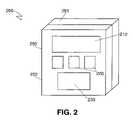
- FIG. 2illustrates a second non-limiting example of control panel 200 for a piece of industrial equipment that includes this invention.
- Control panel 200has a casing 250 having a front cover 252 and a rear cover 251 .
- Casing 250houses all electronics necessary for operation of control panel 200 .
- Front cover 252has openings exposing display 210 , control buttons 220 , and touch pad 230 .
- Display 210is used to display information generated by the electronics in control panel 200 .
- Control buttons 220provide keys that a user may press to perform any of a variety of functions. Control buttons 220 operate in the same manners as keys in keyboard 130 of notebook computer system 100 depicted in FIG. 1 and described above.
- Touch pad 230senses the touch of a user to move through selections on display 210 .
- Touch pad 230may sense the position of a body part in one dimension or two dimensions. For example, touch pad 230 may only sense the vertical position of the body part along the pad or touch pad 230 may sense both the vertical and the horizontal positions of the body part on the pad. Only one dimension is needed when a cursor is only moved in one direction for such functions such as scrolling through a list. However, two dimensions may be needed for moving such functions as moving a cursor across a screen.
- touch pad 230may be positioned in other locations and is shown in this location only for exemplary purposes.
- touch pad 230may be on the side of control panel 200 .
- touch pad 230may also estimate the force or pressure applied to touch pad 230 by a body part of the user by monitoring the area of contact between a user and touch pad 230 . For example, as a user increases the force applied by a finger on touch pad 230 , the finger flattens and splays out, increasing the area of contact between the finger and touch pad 230 .
- This inventionintegrates the sensor elements of the keyboard device and touch pad device into one assembly for easier installation, shorter production time, more efficient material use, and lower production component count.
- the circuit assemblyincludes a preventative capacitance configuration that limits non-intentional capacitive coupling between a capacitive sensor and objects in the environment other than a conductive input object.
- This inventionrelates to the circuit assembly used to provide sensors of the input devices in a system and the conductors that link these sensors to the associated electronics that receive and process detected signals. This invention does not include these associated electronics that receive and process detected signals.
- One skilled in the artwill also recognize some operational modifications of the associated electronics may be needed.
- FIGS. 3–9illustrate the placement of conductive material in switch sensors area 301 and capacitive sensor area 302 on various substrates in circuit assembly 300 .
- FIGS. 10–18illustrate an exemplary embodiment of this invention illustrate the operation of circuit assembly 300 and the preventative capacitance configurations included in circuit assembly 300 in accordance with this invention to limit non-intentional capacitive coupling.
- the preventative capacitance configurationincreases the accuracy of the measured capacitance of conductive material in capacitive sensor 300 to increase the accuracy of properties measured by a capacitive sensor.
- FIG. 3illustrates an isometric view of circuit assembly 300 .
- Circuit assembly 300includes switch sensor area 301 and capacitance sensor area 302 .
- Switch sensor area 301includes the conductive material that provides membrane switch sensors for a keyboard device.
- Capacitance sensor area 302includes the conductive material that provides sensor elements for a touch pad device.
- conductive elements 310 in switch sensor area 301are shown and conductive electrodes 321 of a first layer in capacitive sensor area 302 are shown.
- FIGS. 4 and 5illustrate a cross section of circuit assembly 300 along line 199 to illustrate a circuit assembly 300 having a portion of one layer of conductive material in capacitive sensor area 302 .
- One layer of conductive material of conductive materialis used to measure a one-dimensional property.
- One-dimensional propertiesinclude but are not limited to position of the conductive input device along one axis.
- FIG. 4illustrates a first layer of conductive material including electrodes 321 in capacitive sensor area 302 . Electrodes 321 are in a first pattern 341 of conductive material that includes conductive elements 310 in switch sensor area 301 .
- switch sensor areahas conductive elements 310 are in a first pattern 341 and conductive elements 312 in second pattern 343 of conductive material.
- First pattern 341is affixed to a bottom side of substrate 303 .
- Second pattern 343is affixed to a top side of substrate 304 in opposition to first pattern 341 .
- Insulating member 342separates first pattern 341 from second pattern 343 and is disposed between first pattern 341 and second pattern 343 .
- Insulating member 342includes openings 313 that allow electrical contact between mated pairs of conductive elements 310 and conductive elements 312 . The operation of conductive elements 310 and 312 in the switch sensor area 301 and electrodes 321 in capacitance sensor area 302 will be described below in reference to FIG. 10 .
- FIG. 5illustrates a cross sectional view of circuit assembly 300 along line 199 .
- Capacitive sensor area 302has one layer of conductive material illustrated as electrodes 321 .
- electrodes 321are included in second pattern 343 in FIG. 5 instead of in the first pattern 341 as shown in FIG. 4 .
- the remaining elements shown in FIG. 5are configured as described with respect to FIG. 4 .
- FIGS. 6–9illustrate cross sectional views of different embodiments of circuit assembly 300 along line 199 .
- capacitive sensor area 302includes a first layer and second layer of conductive materials.
- the first layeris represented by electrodes 321 .
- the second layeris represented by electrodes 323 .
- four different embodimentsare shown, one skilled in the art will recognize that any combination of the two layers may be used. This includes having one layer in first pattern 341 or in second pattern 343 and the second layer in a third pattern.
- the third patternmay be the remaining one of first and second patterns 341 and 343 or in a third pattern elsewhere in circuit assembly 300 .
- FIG. 6illustrates a first layer of conductive material including electrodes 321 and a second layer of conductive material including electrodes 323 in capacitive sensor area 302 .
- Electrodes 321are in a first pattern 341 of conductive material that includes conductive elements 310 in switch sensor area 301 .
- Electrodes 323are in a second pattern 343 of conductive material that includes conductive elements 312 in switch sensor area 301 .
- first pattern 341is affixed to a bottom side of substrate 303 .
- Second pattern 343is affixed to a top side of substrate 304 in opposition to first pattern 341 .
- Insulating member 342separates first pattern 341 from second pattern 343 and is disposed between first pattern 341 and second pattern 343 .
- Insulating member 342includes openings 313 that allow electrical contact between mated pairs of conductive elements 310 and conductive elements 312 in switch sensor area 301 .
- capacitive sensor area 302insulating member 342 maintains separation between electrodes 321 and 323 . The operation of conductive elements 310 and 312 in the switch sensor area 301 and electrodes 321 and 323 in capacitance sensor area 302 will be described below in reference to FIG. 10 .
- FIG. 7illustrates a cross sectional view along line 199 of a second embodiment of circuit assembly 300 having two layers of conductive material in capacitive sensor area 302 .
- electrodes 323are in a third pattern 344 of conductive material.
- Third pattern 344is in a plane that is substantially parallel to first pattern 341 , second pattern 343 , and insulating member 342 .
- third pattern 344is affixed to a top side of substrate 303 that is opposite of the side of substrate 303 to which first pattern 341 is affixed.
- the other components of circuit assembly 300 shown in FIG. 7are configured as described with reference to FIG. 6 .
- FIG. 8illustrates a cross sectional view along line 199 of a third embodiment of circuit assembly 300 having two layers of conductive material in capacitive sensor area 302 .
- electrodes 323are in a third pattern 344 of conductive material.
- Third pattern 344is in a plane that is substantially parallel to first pattern 341 , second pattern 343 , and insulating member 342 .
- third pattern 344is affixed to inner surface of textured material 1001 .
- the other components of circuit assembly 300 shown in FIG. 8are configured as described with reference to FIG. 6 .
- FIG. 9illustrates a cross sectional view along line 199 of a fourth embodiment of circuit assembly 300 having two layers of conductive material in capacitive sensor area 302 .
- electrodes 323are in a third pattern 344 of conductive material.
- Third pattern 344is in a plane that is substantially parallel to first pattern 341 , second pattern 343 , and insulating member 342 .
- Third pattern 344is affixed to a top side of a rigid substrate 398 .
- Rigid substrate 398is a printed circuit board in an exemplary embodiment.
- the other components of circuit assembly 300 shown in FIG. 9are configured as described with reference to FIG. 6 .
- FIG. 10illustrates an exploded view of an exemplary sensor circuit assembly 300 for use in notebook computer system 100 (shown in FIG. 1 ) in accordance with this invention.
- Circuit assembly 300has a membrane switch sensor area 301 and a capacitive sensor area 302 and a preventive capacitance configuration.
- switch sensor area 301 and capacitive sensor area 302are one circuit assembly 300 and the preventative capacitance configuration includes circuitry and components which limit non-intentional capacitive coupling between conductive material in capacitance sensor area 302 and other objects.
- circuit assembly 300may be one circuit assembly or any other one piece integrated component for providing the sensors.
- circuit assembly 300may be one circuit assembly or any other one piece integrated component for providing the sensors.
- other types of sensorsmay be added to this circuit assembly, including but not limited to knobs, switches, duraswitches, and resistive touch sensors.
- An exemplary membrane switch sensoroperates in the following manner.
- a first conductive element 310is in a first pattern 341 of conductive material and is connected to keyboard electronics 392 via conductor 311 .
- a conductive elementis a contact pad, electrode, or other type of conductive circuitry.
- a second element 312is aligned with first conductive element 310 and is connected to keyboard electronics 392 via conductor 319 .
- Second conductive element 312is on a second pattern 343 of conductive material located underneath first pattern 341 .
- Second conductive element 312is separated from first conductive element 310 by insulating member 342 .
- Second conductive element 312normally does not contact first conductive element 310 without user input.
- first conductive element 310is depressed by user force to contact second conductive element 312 through opening 313 in insulating member 342 .
- Capacitive sensor area 302provides a capacitive sensor that operates in the following manner.
- First electrodes 321are aligned substantially parallel to one another in a first direction and are spaced evenly apart on a first layer in plane A.
- Conductors 324connect first electrodes 321 to capacitive sensor electronics 391 .
- First electrodes 321measure a position of a conductive object along a path substantially perpendicular to the first direction.
- Second electrodes 323are aligned parallel to one another in a second direction and spaced evenly apart in a plane A′′.
- the second directionis orthogonal to the first direction.
- the first and second axesneed only be skewed and non-parallel such that the axes are not parallel and span a plane.
- Conductors 325connect second electrodes 323 to capacitive sensor electronics 391 .
- Capacitance electronics 391measures the capacitance of each of the first group of electrodes 321 and the second group of electrodes 323 . From the measured capacitance each of the first electrodes, electronics 391 determines the position of the conductive input object in the direction substantially orthogonal to the first direction within sensor area 302 . From the measured capacitance of each of the second electrodes 323 , electronics 391 determines the position of the conductive input object in the direction substantially orthogonal to the second direction within sensor area 302 .
- the measured capacitance of the electrodesmay also be used to measure other properties, such as pressure of touch.
- the capacitive touch pad devicedoes not require physical contact between electrodes in the first and second groups of electrodes 321 and 323 to determine the position of the conductive input object. Further, one skilled in the art will also note that the capacitive touch pad device does not require movement of either the first group of electrodes 321 or the second group of electrodes 323 to determine position of the conductive object. It should also be noted that the position of a conductive input object may be measured in one dimension using one of either the first or second group of electrodes 321 , 323 .
- first or second groups of electrodes 321 , 323needs to be present in capacitive touch sensor area 302 .
- the layout and configuration of the group of electrodeswill depend on the desired sensing area and sensing dimension, and may differ from that shown in FIG. 10 .
- membrane switch electronics 392 and capacitive sensor electronics 391are shown as separate components as is standard in the prior art, it is possible to combine electronics 391 and 392 into one integrated circuit. Also it is possible for electronics 391 , 392 to share common components such as a power supply and power conditioning electronics or to share the same physical connection to a host system.
- circuit assembly 300is constructed in the following manner.
- Circuit assembly 300has a first pattern of conductive material 341 , a second pattern of conductive material 343 , and an insulating member 342 .
- Circuit assembly 300includes a switch sensor area 301 and a capacitive sensor area 302 .
- First pattern of conductive material 341includes conductive elements 310 from switch sensor area 301 and first electrodes 321 of capacitive sensor area 302 .
- First pattern of conductive material 341is in a first plane A.
- Conductive elements 310may be contact pads or electrodes that are conductive.
- first pattern 341may include conductive material affixed to a first substrate or may be a first substrate of material with traces of conductive ink.
- Insulating member 342separates first pattern 341 and second pattern 343 .
- Insulating memberis oriented in a plane A′. Plane A′ is substantially parallel to Plane A.
- insulating member 342may be a solid sheet of insulating material as shown in FIG. 10 , a spacer that physically separates first pattern 341 from second pattern 342 and forms air gaps between first pattern 341 and second pattern 342 as shown in FIG. 12 and described below, or a series of insulating bumps that maintain separation between first pattern 341 and second pattern 343 as shown in FIG. 12 as described below.
- insulating member 342has openings 313 or other structures which allow conductive elements 310 to make electrical contact with mated conductive elements 312 in second pattern 343 in response to a force exerted in direction D.
- capacitive sensor area 302insulating member 342 maintains spacing between electrodes 321 in the first pattern 341 and electrodes 323 in second pattern 343 . This helps limit the relative motion between electrodes 321 and 323 that may change the capacitance sensed by capacitance touch pad electronics 391 and give an invalid reading of the position of the conductive object.
- Second pattern of conductive material 343is in a plane A′′ which is substantially parallel to planes A and A′. Second pattern 343 has conductive elements 312 in switch sensor area 301 . Each conductive element 312 is aligned with a conductive element 310 in first pattern 341 . Each aligned conductive element 312 opposes the corresponding aligned conductive element 310 and is directly underneath aligned conductive element 310 .
- second pattern 343may include conductive material affixed to a second substrate or may be a second substrate of material with traces of conductive ink.
- second pattern of conductive material 343must be affixed or traced onto the second substrate in manner that allows electrical contact between conductive elements 310 and conductive elements 312 in switch sensor area 301 .
- second pattern 343includes second electrodes 323 .
- Second electrodes 323are aligned in a second direction that is substantially orthogonal to the first direction.
- the first and second axesneed only be skewed such that the axes are not parallel and span a plane for the capacitance touch pad device to properly sense the position of the conductive object in two dimensions.
- first or second conductors 321 – 323may be omitted if the position only needs to be measured along one axis.
- only discrete conductive pads, and not groups of electrodesare necessary if only the presence or size of the touch (and not the position or motion) is desired.
- the second patternmay be affixed to a substrate such as conductive ink traces defining individual components on an insulating material.
- a capacitive sensormay be deposited on first pattern 341 and second pattern 343 .
- the preventative capacitance configuration of circuit assembly 300may include a conductor 351 on the first pattern and/or a conductor 352 in the second pattern 343 .
- Conductors 351 and 352are held at a substantially constant voltage such as but not limited to ground.
- conductors 351 and 352are held at a voltage that reduces the magnitude of signals in membrane switch sensor area 301 from being received by first and second electrodes 321 and 323 .
- Received signals from membrane switch sensor area 301may affect electrodes 321 and 323 giving an invalid reading of the position of the conductive object.
- conductor 351 on first pattern 341may be in locations on first pattern 341 that shield conductive material in second pattern 343 from objects in the environment.
- conductor 352may be in locations on second pattern 343 that shield conductive material in first pattern 341 from objects in the environment.
- switch sensor area 301 and capacitive area 302may be spaced far enough apart in circuit assembly 300 to prevent electrodes and conductors of capacitive sensor area 302 from receiving signals from switch sensor area 301 .
- the preventative capacitance configurationmay include conductor 396 placed on insulating member 342 .
- Conductor 396is held at a substantially constant voltage, such as ground.
- Conductor 396is placed on insulating member where there is little or no probability of shorting with conductive components of first pattern 341 or second pattern 342 .
- Conductor 396may be used shield the conductive components of first pattern 341 and second pattern 343 from extraneous signals or capacitive coupling with objects in the environment.
- conductor 396is a trace of conductive material deposited on insulating member 342 .
- Conductor 396may also be used as shielding between at least a portion of first pattern 341 and second pattern 343 to reduce non-intended capacitive coupling between conductive material in first pattern 341 and second pattern 343 .
- openings in insulating member 342may be used instead of conductor 396 .
- the openingsdefine air gaps between the conductive material of first pattern 341 and second pattern 343 to reduce the non-intended capacitive coupling.
- Circuit assembly 300connects conductive element 310 to keyboard electronics 392 via conductors 311 .
- conductors 311are conductive traces in first pattern 341 .
- Conductive elements 312 in second pattern 343are connected to keyboard electronics 392 via conductors 319 .
- conductors 319are traces of conductive material in second pattern 343 .
- the conductive tracesmay be made of conductive inks such as but not limited to silver ink or carbon ink.
- any configuration of conductive materialmay be used to provide the conductors.
- First electrodes 321connect to capacitive sensor electronics 391 via conductors 324 .
- conductors 324are traces of conductive materials along first pattern 341 .
- the conductors 324may be routed to electronics 391 in any number of ways.
- conductors 324may be as short and as thin as reasonable to decrease the area of coverage of conductors 324 .
- conductors 324may be routed around areas on first pattern 341 corresponding to areas, such as hand rests 155 of casing 150 (Shown in FIG. 1 ), proximate to other objects in the environment.
- Conductors 324may also be routed around areas within casing 150 where electronics and systems not directly related to circuit assembly 300 may be located. Non-intended capacitive coupling to conductors 324 must be reduced since such non-intended capacitive coupling changes the capacitance measured by capacitive sensor electronics 391 connected to conductors 324 and introduces errors in the reading of the position of a conductive input object over the sensor.
- One skilled in the artwill recognize that only a portion of the conductors may be routed around areas corresponding to other objects in the environment, such as hand rests 155 , depending on a variety of factors including but not limited to manufacturing and design constraints as well as considerations regarding decreasing the lengths and sizes of the conductors 324 .
- One skilled in the artwill further recognize that combining keyboard sensor electronics 391 and capacitive sensing electronics 391 allows a single connector to connect conductors 311 and 324 to the respective electronics 391 , 392 .
- the preventative capacitance configurationmay include a conductor (Not Shown) on top cover 151 held at a substantially constant voltage over at least a portion of conductors 324 to reduce undesirable capacitive coupling with objects in the environment.
- An alternate embodiment of this conductormay include, but not be limited to, conductive material deposited on a substrate and attached to top cover 151 , conductive material deposited, painted or otherwise placed on top cover 151 , and conductive material embedded within top cover 151 .
- these shielding alternativesmay be used in combination or individually to reduce capacitive coupling between the conductors and the other objects in the environment.
- Conductors 325connect second electrodes 323 to capacitive sensor electronics 391 .
- conductors 325are traces of conductive material in second pattern 343 .
- switch sensor electronics 392 and capacitive sensor electronics 391are combined, a single connector allows conductors 312 and 324 to connect to the respective electronics 391 , 392 .
- conductors 325may be connected to sensor electronics 391 in any number of ways. To reduce undesirable capacitive coupling with the environment, conductors 325 may be made as short or as thin as reasonable to decrease the area of coverage for conductors 325 .
- the preventative capacitance configurationmay include conductors 325 routed around areas of pattern 343 corresponding to area proximate other items in the environment, such as hand rests 155 of casing 150 (Shown in FIG. 1 ). Conductors 325 may also be routed around areas inside casing 150 where electronics and other systems not directly related to circuit assembly 300 may be located. One skilled in the art will recognize that only a portion of conductors 325 may be routed around areas corresponding to rest areas 155 depending on a variety of factors including but not limited to manufacturing and design constraints as well as considerations regarding the decreasing of the lengths and sizes of conductors 325 .
- the preventative capacitance configurationmay include a conductor (Not Shown) affixed to bottom cover 152 of casing 150 .
- the conductor (Not Shown)is held at a substantially constant voltage and is affixed to the inner surface of bottom cover 152 , embedded within bottom cover 152 , or attached to the outer surface of bottom cover 152 .
- first pattern 341 , and second pattern 343are important.
- switch sensor area 301alignment of a conductive element 310 with mated conductive element 312 and opening 313 must be maintained to allow contact between the contact pads in response to a force generated by keystroke input from the user.
- capacitive sensor area 302alignment of first electrodes 321 with respect to second electrodes 323 is important to determine the position of a conductive object over the electrodes. Misalignment may cause inaccurate position determinations by capacitance measuring electronics 391 .
- circuit assembly 300may have a coupling of the substrates on which first pattern 341 and second pattern 343 are affixed or traced.
- Insulating member 342may also be coupled to first pattern 341 and second pattern 343 .
- One manner of couplingis to deposit first pattern 341 and second pattern 343 on two sides of one substrate, such as insulating member 342 . The alignment then becomes a function of manufacturing.
- first pattern 341 and second pattern 343are deposited on separate substrates
- one manner of coupling first pattern 341 and second pattern 343is having structural members 395 protruding from an inside surface of casing 150 .
- structural members 395protrude upward from bottom cover 152 .
- structural members 395may also protrude from an inside of top cover 151 (not shown).
- Structural members 395pass through mated openings 360 , 361 in the substrates of first and second patterns 341 , 343 and openings 370 in insulating member 342 .
- openings 370are not needed if insulating member 342 does not extend over openings 360 , 361 .
- structural members 395should be placed such that structural members 395 do not introduce undesirable deformation or motion within capacitive sensor area 302 during use.
- Each structural member 395may be an extension of the casing 150 or a separate component attached to the casing 150 .
- Each structural member 395may be a screw or other standard fastener that attaches casing 150 to components (Not Shown) connected with casing 150 .
- first pattern 341 and second pattern 343An alternative manner for coupling first pattern 341 and second pattern 343 is to provide nibs (not shown) on opposing sides of insulating member 342 which are mated to openings 360 , 361 in the substrates of first pattern 341 and second pattern 343 .
- the openings 360 , 361fit over the nibs to hold first pattern 341 and second pattern 343 in place with respect to one another.
- the nibsshould be placed such that nibs do not introduce undesirable deformation or motion within capacitive sensor area 302 during use.
- Another manner of couplingmay be to heat stake the substrate of first pattern 341 and the substrate of second pattern 343 to one another.
- the heat stakingmay be done at the edges or at particular points in circuit assembly 300 away from conductive components.
- Another manner of couplingmay be to adhere the substrates of first pattern 341 and second pattern 343 to one another.
- the adhesionmay be done at the edges of the substrates containing patterns, at particular points in circuit assembly 300 , or over entire regions of circuit assembly 300 including capacitive sensor area 302 . The only requirement is that the adhesion does not prevent the proper switching action from occurring with in switch sensor area 301 .
- These methods of coupling listed abovemay also be extended to align insulating member 342 to first pattern 341 and/or second pattern 343 .
- first pattern 341 , insulating member 342 , and/or second pattern 343may also make circuit assembly 300 more rigid. Added rigidity reduces deformations of first and second patterns 341 , 343 during use that may reduce the sensitivity of the capacitive sensor device, introduce error to readings of position, or indicate false contacts in switch area 301 .
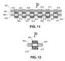
- FIG. 11shows a cross sectional view of a portion of switch sensor area 301 in circuit assembly 300 .
- First pattern 341has conductive elements 310 space apart from one another.
- Insulating member 342has openings 313 through insulating member 342 which allow conductive elements 310 to pass through in response to a force being exerted on the contact in direction D.
- Second pattern 343has conductive elements 312 that are mated to openings 313 and conductive elements 310 .
- a layer of tactile materialmay be placed over first pattern 341 in switch sensor area 301 .
- the tactile layerprovides an aesthetic feedback to a user pressing keys.
- the tactile layermay also add rigidity to circuit assembly 300 .
- FIG. 12is cross sectional view of a section of membrane switch sensor area having an alternative insulating member 342 .
- insulating member 342is made of a plurality of insulating bumps 501 – 502 .
- Aligned conductive elements 310 , 312are positioned in spaces between insulating dots 501 – 502 . This allows conductive element 310 to be forced into contact with conductive element 312 in response to a force in direction D being applied to conductive element 310 .
- FIG. 13illustrates a second alternative for insulating member 342 in membrane switch sensor area 301 in which spacer 602 is used.
- insulating member 342is a spacer 602 .
- Spacer 602is a layer of insulating material around the perimeter a pattern of aligned conductive elements 310 , 312 .
- the pattern of aligned elements 310 , 312make contact through opening 603 of spacer 602 in response to a force in direction D being applied to an element 310 .
- FIG. 14illustrates a cross sectional view of an embodiment of capacitive sensor area 302 in accordance with this invention.
- first electrodes 321 of first pattern 341are affixed to a bottom side of first substrate 701 and second electrodes 323 of second pattern 343 are affixed to a top side of bottom substrate 702 .
- Conductors 324 of first pattern 321are also affixed to the bottom side of top substrate 701 and conductors 325 are on the top side of bottom substrate 702 .
- Insulating member 342separates first pattern 341 and second pattern 343 .
- This designis analogous to that of a conventional keyswitch sensor in which the aligned conductive elements 310 are place on a bottom side of top substrate 701 and conductive elements 312 are placed on a top side of bottom substrate 702 to face one another and facilitate contact in response to a force on a conductive element 310 .
- FIG. 15illustrates a cross section view of another exemplary embodiment of capacitive sensor area 302 .
- Electrodes 321 in first pattern 341are affixed to a first substrate 805 and electrodes 323 of second pattern 343 are affixed to substrate 806 , insulating member 342 is between electrodes 321 and 323 .
- Under substrate 806is a grounding plate 802 that is a conductor held at a substantially constant voltage such as ground.
- grounding plate 802is an insulating substrate 803 .
- grounding plate 802does not actually have to be a plate, but can be any configuration of conductive material.
- Protective layer 801is a layer of material added over first pattern 341 to add stiffness to the circuit assembly and to provide an aesthetic feel for a user.
- protective layer 801is a polyester material.
- FIG. 16illustrates a cross sectional view of a portion of a second exemplary embodiment of capacitive area 302 .
- insulating member 342is an insulating substrate 901 .
- Insulating substrate 901is made of a flexible insulating material that may be folded or formed into any numbers of shapes including the semispherical shape illustrated. Those skilled in the art will appreciate that this allows capacitive sensor area 302 to be shaped into a desired form by a maker of a circuit assembly in accordance with this invention.
- Electrodes 321 of first pattern 341are affixed to a first surface of insulating substrate 901 .
- Electrodes 323 of second pattern 343are affixed to a second surface of insulating substrate 901 .
- the conductive patternscan be deposited on the top or bottom surfaces of the associated substrate, the substrate may act as an insulating member, and more than one insulating member can be interposed between the first and second conductive patterns.
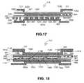
- FIG. 17is a cross sectional view of a first exemplary embodiment of capacitive sensor area 302 of circuit assembly 300 in casing 150 .
- First pattern 341has conductors 321 that are under bezel 141 .
- Bezel 141includes an opening in a top cover 151 of casing 150 .
- Electrodes 321are aligned in a first direction parallel with the cross section.
- Insulating member 342maintains separation between first pattern 341 and second pattern 343 .
- Second pattern 343has electrodes 323 that are aligned substantially orthogonal to electrodes 321 under bezel 141 .
- a layer 1001 of textured materialmay be placed over first pattern 341 .
- the textured material of layer 1001provides an aesthetic sense of touch to the user and may add rigidity to circuit assembly 300 .
- layer 1001is a layer of polyester material over first pattern 341 .
- a boss 1002may be added proximate to bezel 141 , such as around bezel 141 , to clamp capacitive sensor area 302 against a surface inside back cover 152 (Shown in FIG. 1 ). Also, bezel 141 may be used to define air gaps 1003 between first pattern 341 and front cover 151 to reduce capacitive coupling between conductors 324 and resting or nearby body parts.
- brace 1004may be added.
- brace 1004may be an inner surface of a structure inside back cover 152 or a separate structure affixed to front cover 151 and/or back cover 152 .
- Brace 1004includes a localized clamping region 1010 .
- Localized clamping region 1010is a portion of brace 1004 elevated in a direction of second pattern 343 to hold sensor area 302 in place against bezel 141 and/or boss 1002 .
- the elevated clamping region 1010may be used to define air gaps 1005 between second pattern 343 and brace 1004 .
- the air gaps 1005reduce capacitive coupling between conductors 325 and body parts of a user resting on back cover 152 .
- any number of insulating substratesmay be added. These are omitted for clarity.
- FIG. 18illustrates a cross sectional view of a second exemplary embodiment of capacitive sensor area 302 inside a casing 150 .
- bezel 141is a depression 1125 in top cover 151 and does not include an opening.
- Electrodes 321are substantially parallel to the cross section and proximate depression 1125 .
- the material of casing 150is thin enough at depression 1125 to allow changes in capacitance in electrodes 321 and 323 when a body part of a user is proximate depression 1125 .
- top cover 151can be textured within capacitive sensor area 302 to yield an aesthetic fell of touch or a layer of textured material (not shown) can be placed on top cover 151 .
- First pattern 341is affixed to a first insulating substrate layer 1110 and second pattern 343 is affixed to a second insulating substrate layer 1111 .
- first insulating substrate layer 1110and second pattern 343 is affixed to a second insulating substrate layer 1111 .
- insulating substrate layersare added for rigidity and not essential to this invention.
- insulating member 342is made of insulating spacers 1106 .
- Insulating spacers 1106define air gaps 1105 that prevent cross capacitance between electrodes.
- spacers 1106define air gaps 1105 in areas corresponding to an intersection of electrodes 321 crossing over electrodes 323 as part of the preventative capacitance configuration.
- air gaps 1105may be defined by openings in a solid sheet of insulating material when insulating member 342 is a solid piece of insulating material.
- the preventative capacitance configurationmay include grounding plate 1104 in capacitive sensor area 302 .
- Grounding plate 1104is between second pattern 343 and brace 1004 .
- Grounding plate 1104is a conductor held at a substantially constant voltage, such as ground. This reduces capacitive coupling between other objects on or near back cover 152 and electrodes 321 and/or conductors 324 . This also reduces non-intended capacitive coupling between other objects near back cover 152 and electrodes 323 and/or conductors 325 .
- grounding plate 1104may be included in other embodiments that do not include brace 1004 between capacitive sensor area 302 and back cover 152 .
- the preventative capacitance configurationmay also include grounding plate 1116 .
- Ground plates 1116may also be included to prevent capacitive coupling between conductors 324 and other objects near or resting on top cover 151 .
- Ground plates 1116are affixed to an inner surface of top cover 151 over first pattern 341 .
- Ground plates 1116are conductors held a substantially constant voltage, such as ground.
- ground plates 1116may be used in other embodiments that do not have the bezel 141 described in FIG. 18 .
Landscapes
- Engineering & Computer Science (AREA)
- General Engineering & Computer Science (AREA)
- Theoretical Computer Science (AREA)
- Human Computer Interaction (AREA)
- Physics & Mathematics (AREA)
- General Physics & Mathematics (AREA)
- Switches That Are Operated By Magnetic Or Electric Fields (AREA)
Abstract
Description
Claims (88)
Priority Applications (1)
| Application Number | Priority Date | Filing Date | Title |
|---|---|---|---|
| US10/251,563US6943705B1 (en) | 2002-05-03 | 2002-09-19 | Method and apparatus for providing an integrated membrane switch and capacitive sensor |
Applications Claiming Priority (2)
| Application Number | Priority Date | Filing Date | Title |
|---|---|---|---|
| US37793202P | 2002-05-03 | 2002-05-03 | |
| US10/251,563US6943705B1 (en) | 2002-05-03 | 2002-09-19 | Method and apparatus for providing an integrated membrane switch and capacitive sensor |
Publications (1)
| Publication Number | Publication Date |
|---|---|
| US6943705B1true US6943705B1 (en) | 2005-09-13 |
Family
ID=34915324
Family Applications (1)
| Application Number | Title | Priority Date | Filing Date |
|---|---|---|---|
| US10/251,563Expired - Fee RelatedUS6943705B1 (en) | 2002-05-03 | 2002-09-19 | Method and apparatus for providing an integrated membrane switch and capacitive sensor |
Country Status (1)
| Country | Link |
|---|---|
| US (1) | US6943705B1 (en) |
Cited By (81)
| Publication number | Priority date | Publication date | Assignee | Title |
|---|---|---|---|---|
| US20040027385A1 (en)* | 2001-02-19 | 2004-02-12 | Junichi Rekimoto | Information input device |
| US20050246459A1 (en)* | 2003-07-11 | 2005-11-03 | Harald Philipp | Keyboard With Reduced Keying Ambiguity |
| US20060001655A1 (en)* | 2004-07-01 | 2006-01-05 | Koji Tanabe | Light-transmitting touch panel and detection device |
| US20060002203A1 (en)* | 2004-07-01 | 2006-01-05 | Alps Electric Co., Ltd. | Input device having activating means |
| US20060017708A1 (en)* | 2004-07-26 | 2006-01-26 | Toshiharu Fukui | Input device |
| US20060033722A1 (en)* | 2004-08-13 | 2006-02-16 | Yen-Chang Chiu | Structure and mechanism for power-saving of a capacitive touchpad |
| US20060044259A1 (en)* | 2004-08-25 | 2006-03-02 | Hotelling Steven P | Wide touchpad on a portable computer |
| US20060043562A1 (en)* | 2004-08-31 | 2006-03-02 | Yoshio Watanabe | Circuit device and manufacture method for circuit device |
| US20060060459A1 (en)* | 2004-09-22 | 2006-03-23 | Alps Electric Co., Ltd. | Operation device |
| US20060192690A1 (en)* | 2002-07-12 | 2006-08-31 | Harald Philipp | Capacitive Keyboard with Non-Locking Reduced Keying Ambiguity |
| US20070018965A1 (en)* | 2005-07-22 | 2007-01-25 | Tyco Electronics Canada, Ltd. | Illuminated touch control interface |
| US20070163865A1 (en)* | 2006-01-17 | 2007-07-19 | Huo-Lu Tsai | Thin film circuit board of keyboard |
| US20070164994A1 (en)* | 2006-01-18 | 2007-07-19 | Takefumi Inoue | Input device |
| US20070242037A1 (en)* | 2006-04-14 | 2007-10-18 | Son Jae S | Electronic device housing with integrated user input capability |
| US20070257821A1 (en)* | 2006-04-20 | 2007-11-08 | Son Jae S | Reconfigurable tactile sensor input device |
| WO2008026882A1 (en)* | 2006-08-30 | 2008-03-06 | Rechner Korea Co., Ltd. | Capacitance type leakage sensor |
| US20080142352A1 (en)* | 2006-12-18 | 2008-06-19 | Wright David G | Two circuit board touch-sensor device |
| US20080252608A1 (en)* | 2007-04-12 | 2008-10-16 | 3M Innovative Properties Company | Touch sensor with electrode array |
| US20080302583A1 (en)* | 2004-09-27 | 2008-12-11 | Kazuo Tateishi | Gas Cell for Electrostatic Induction Type Touch Input Device |
| WO2008136928A3 (en)* | 2007-04-30 | 2009-01-29 | Daktronics | Capacitive relay takeoff swimming platform sensor system |
| US20090040191A1 (en)* | 2007-08-08 | 2009-02-12 | Synaptics Incorporated | Capacitive touch sensor with conductive trace lines in bonding region |
| US20090096763A1 (en)* | 2007-10-16 | 2009-04-16 | Epson Imaging Devices Corporation | Touch panel, display device with input function, and electronic apparatus |
| US7538288B1 (en)* | 2008-03-31 | 2009-05-26 | Mildex Optical Inc. | Touch panel |
| US20090142477A1 (en)* | 2007-11-30 | 2009-06-04 | Asustek Computer Inc. | Portable electronic device and transferring method of circuit element thereof |
| US20090174679A1 (en)* | 2008-01-04 | 2009-07-09 | Wayne Carl Westerman | Selective Rejection of Touch Contacts in an Edge Region of a Touch Surface |
| US7561146B1 (en) | 2004-08-25 | 2009-07-14 | Apple Inc. | Method and apparatus to reject accidental contact on a touchpad |
| US20090267903A1 (en)* | 2008-04-23 | 2009-10-29 | Motorola, Inc. | Multi-Touch Detection Panel with Disambiguation of Touch Coordinates |
| US20090288871A1 (en)* | 2008-05-23 | 2009-11-26 | Chih-Tsung Lin | Thin film circuit board device |
| US20090314550A1 (en)* | 2008-06-18 | 2009-12-24 | Layton Michael D | Touchpad designed in a planar configuration that can be molded to conform to a non-planar object |
| US20100045620A1 (en)* | 2008-07-23 | 2010-02-25 | Ding Hua Long | Integration design for capacitive touch panels and liquid crystal displays |
| US20100108360A1 (en)* | 2008-11-05 | 2010-05-06 | Wen-Yu Tsai | Membrane circuit board |
| WO2010059216A1 (en)* | 2008-11-20 | 2010-05-27 | Cirque Corportion | Method and system for measuring position on surface capacitance touch panel using a flying capacitor |
| US20100139955A1 (en)* | 2008-12-05 | 2010-06-10 | Ding Hua Long | Capacitive touch panel having dual resistive layer |
| US20100156811A1 (en)* | 2008-12-22 | 2010-06-24 | Ding Hua Long | New pattern design for a capacitive touch screen |
| US20100220076A1 (en)* | 2009-02-27 | 2010-09-02 | Kyocera Corporation | Input Device and Display Device Including the Same |
| US20100245246A1 (en)* | 2009-03-30 | 2010-09-30 | Microsoft Corporation | Detecting touch on a curved surface |
| US20100242274A1 (en)* | 2009-03-30 | 2010-09-30 | Microsoft Corporation | Detecting touch on a curved surface |
| US20100328241A1 (en)* | 2009-06-12 | 2010-12-30 | Keith Paulsen | Method and system for measuring position on surface capacitance touch panel using a flying capacitor |
| US20110011650A1 (en)* | 2009-07-15 | 2011-01-20 | Sony Ericsson Mobile Communications Ab | Sensor assembly and display including a sensor assembly |
| US20110043481A1 (en)* | 1998-10-09 | 2011-02-24 | Frederick Johannes Bruwer | User interface with proximity sensing |
| US20110057904A1 (en)* | 2009-09-07 | 2011-03-10 | Ikuo Yamano | Sensor Device and Information Processing Device |
| US20110115652A1 (en)* | 2009-11-13 | 2011-05-19 | Research In Motion Limited | Detection of intended key activation on a mobile device |
| US20110186414A1 (en)* | 2010-02-04 | 2011-08-04 | Pantech Co., Ltd. | Dome switch integrated touch window for mobile terminal |
| US20110193803A1 (en)* | 2008-07-04 | 2011-08-11 | Electrolux Home Products Corporation N.V. | Input device |
| WO2011137382A3 (en)* | 2010-04-30 | 2012-01-19 | Ikey, Ltd. | Panel mount keyboard system |
| US20120120017A1 (en)* | 2010-11-17 | 2012-05-17 | Synaptics Incorporated | System and method for determining object information using an estimated deflection response |
| US20120206354A1 (en)* | 2011-02-14 | 2012-08-16 | Ko Ja (Cayman) Co., Ltd. | Integrated input apparatus |
| USRE43606E1 (en) | 2004-06-25 | 2012-08-28 | Azoteq (Pty) Ltd | Apparatus and method for a proximity and touch dependent user interface |
| US8274486B2 (en) | 2008-12-22 | 2012-09-25 | Flextronics Ap, Llc | Diamond pattern on a single layer |
| US20120262005A1 (en)* | 2006-03-21 | 2012-10-18 | Murata Manufacturing Co., Ltd. | Device for transporting energy by partial influence through a dielectric medium |
| US20130081856A1 (en)* | 2011-09-29 | 2013-04-04 | Tse-Kun Chang | Touch panel |
| US8445793B2 (en) | 2008-12-08 | 2013-05-21 | Apple Inc. | Selective input signal rejection and modification |
| TWI402726B (en)* | 2008-10-07 | 2013-07-21 | Mitac Int Corp | Electronic device and display system with integrated touch screen and control method thereof |
| TWI402734B (en)* | 2009-03-03 | 2013-07-21 | Tpk Touch Solutions Inc | Touch device integrated with capacitive and resistive sensing operation |
| US20130194192A1 (en)* | 2009-03-13 | 2013-08-01 | Adobe Systems Incorporated | Surface scanning with a capacitive touch screen |
| US8525955B2 (en) | 2012-01-31 | 2013-09-03 | Multek Display (Hong Kong) Limited | Heater for liquid crystal display |
| US8624837B1 (en) | 2011-03-28 | 2014-01-07 | Google Inc. | Methods and apparatus related to a scratch pad region of a computing device |
| US20140306724A1 (en)* | 2012-04-11 | 2014-10-16 | Ford Global Technologies, Llc | Proximity switch assembly having groove between adjacent proximity sensors |
| WO2015021330A1 (en)* | 2013-08-07 | 2015-02-12 | Synaptics Incorporated | Capacitive sensitive using a matrix electrode pattern |
| US9128568B2 (en) | 2008-07-30 | 2015-09-08 | New Vision Display (Shenzhen) Co., Limited | Capacitive touch panel with FPC connector electrically coupled to conductive traces of face-to-face ITO pattern structure in single plane |
| US9285929B2 (en) | 2010-03-30 | 2016-03-15 | New Vision Display (Shenzhen) Co., Limited | Touchscreen system with simplified mechanical touchscreen design using capacitance and acoustic sensing technologies, and method therefor |
| US9367151B2 (en) | 2005-12-30 | 2016-06-14 | Apple Inc. | Touch pad with symbols based on mode |
| US9520875B2 (en) | 2012-04-11 | 2016-12-13 | Ford Global Technologies, Llc | Pliable proximity switch assembly and activation method |
| US9548733B2 (en) | 2015-05-20 | 2017-01-17 | Ford Global Technologies, Llc | Proximity sensor assembly having interleaved electrode configuration |
| US9559688B2 (en) | 2012-04-11 | 2017-01-31 | Ford Global Technologies, Llc | Proximity switch assembly having pliable surface and depression |
| US9568527B2 (en) | 2012-04-11 | 2017-02-14 | Ford Global Technologies, Llc | Proximity switch assembly and activation method having virtual button mode |
| US9654103B2 (en) | 2015-03-18 | 2017-05-16 | Ford Global Technologies, Llc | Proximity switch assembly having haptic feedback and method |
| US9660644B2 (en) | 2012-04-11 | 2017-05-23 | Ford Global Technologies, Llc | Proximity switch assembly and activation method |
| TWI587201B (en)* | 2007-01-03 | 2017-06-11 | 蘋果公司 | Capacitive touch sensor panel, method for shielding a capacitive touch sensor panel, and computing device for detecting a touch |
| US9830036B2 (en) | 2007-01-03 | 2017-11-28 | Apple Inc. | Proximity and multi-touch sensor detection and demodulation |
| US9831870B2 (en) | 2012-04-11 | 2017-11-28 | Ford Global Technologies, Llc | Proximity switch assembly and method of tuning same |
| US9944237B2 (en) | 2012-04-11 | 2018-04-17 | Ford Global Technologies, Llc | Proximity switch assembly with signal drift rejection and method |
| US10038443B2 (en) | 2014-10-20 | 2018-07-31 | Ford Global Technologies, Llc | Directional proximity switch assembly |
| US10112556B2 (en) | 2011-11-03 | 2018-10-30 | Ford Global Technologies, Llc | Proximity switch having wrong touch adaptive learning and method |
| US10139870B2 (en) | 2006-07-06 | 2018-11-27 | Apple Inc. | Capacitance sensing electrode with integrated I/O mechanism |
| US10175832B2 (en) | 2011-12-22 | 2019-01-08 | Quickstep Technologies Llc | Switched-electrode capacitive-measurement device for touch-sensitive and contactless interfaces |
| US10180732B2 (en) | 2006-10-11 | 2019-01-15 | Apple Inc. | Gimballed scroll wheel |
| US10353565B2 (en) | 2002-02-25 | 2019-07-16 | Apple Inc. | Input apparatus and button arrangement for handheld device |
| US10503328B2 (en) | 2011-06-16 | 2019-12-10 | Quickstep Technologies Llc | Device and method for generating an electrical power supply in an electronic system with a variable reference potential |
| US10976581B2 (en)* | 2017-02-06 | 2021-04-13 | Sharp Kabushiki Kaisha | Display device |
| US20240329765A1 (en)* | 2023-03-27 | 2024-10-03 | Cirque Corporation | Pressure Capacitive Reference Fixed to a Housing |
Citations (24)
| Publication number | Priority date | Publication date | Assignee | Title |
|---|---|---|---|---|
| US4373122A (en)* | 1981-01-26 | 1983-02-08 | W. H. Brady Co. | Capacitance switch |
| US4444998A (en) | 1981-10-27 | 1984-04-24 | Spectra-Symbol Corporation | Touch controlled membrane for multi axis voltage selection |
| US4484026A (en) | 1983-03-15 | 1984-11-20 | Koala Technologies Corporation | Touch tablet data device |
| US4494105A (en) | 1982-03-26 | 1985-01-15 | Spectra-Symbol Corporation | Touch-controlled circuit apparatus for voltage selection |
| US4587378A (en) | 1984-07-30 | 1986-05-06 | Koala Technologies Corporation | Two-layer touch tablet |
| US4733222A (en) | 1983-12-27 | 1988-03-22 | Integrated Touch Arrays, Inc. | Capacitance-variation-sensitive touch sensing array system |
| US4855550A (en)* | 1988-01-04 | 1989-08-08 | General Electric Company | White touch pads for capacitive touch control panels |
| US4857684A (en)* | 1988-10-25 | 1989-08-15 | W. H. Brady Co. | Capacitance membrane switchcore with intertrace capacitive coupling and/or intratrace capacitive coupling |
| US4975676A (en) | 1989-11-13 | 1990-12-04 | Spectra Symbol Corp. | Glass membrane touch-controlled circuit apparatus for voltage selection |
| US5666096A (en) | 1995-06-02 | 1997-09-09 | Van Zeeland; Anthony J. | Switch with magnetically-coupled armature |
| US5760715A (en)* | 1996-04-15 | 1998-06-02 | Pressenk Instruments Inc. | Padless touch sensor |
| US5796355A (en)* | 1996-05-13 | 1998-08-18 | Zurich Design Laboratories, Inc. | Touch switch |
| US5844506A (en)* | 1994-04-05 | 1998-12-01 | Binstead; Ronald Peter | Multiple input proximity detector and touchpad system |
| US5867111A (en)* | 1993-03-29 | 1999-02-02 | Donnelly Technology, Inc. | Touch control system |
| US5867082A (en) | 1995-06-02 | 1999-02-02 | Duraswitch, Inc. | Switch with magnetically-coupled armature |
| US5990772A (en) | 1995-06-02 | 1999-11-23 | Duraswitch Industries, Inc. | Pushbutton switch with magnetically coupled armature |
| US6023213A (en) | 1999-08-11 | 2000-02-08 | Duraswitch Industries, Inc. | Relocatable knob retention for magnetically actuated switch |
| US6069552A (en) | 1999-06-02 | 2000-05-30 | Duraswitch Industries, Inc. | Directionally sensitive switch |
| US6137387A (en) | 2000-01-10 | 2000-10-24 | Duraswitch Industries, Inc. | Magnetically-retained armature retainer for electrical switches |
| US6262646B1 (en) | 1999-10-18 | 2001-07-17 | Duraswitch Industries, Inc. | Island switch |
| WO2001052416A1 (en) | 2000-01-11 | 2001-07-19 | Cirque Corporation | Flexible touchpad sensor grid for conforming to arcuate surfaces |
| US6459424B1 (en)* | 1999-08-10 | 2002-10-01 | Hewlett-Packard Company | Touch-sensitive input screen having regional sensitivity and resolution properties |
| US6723933B2 (en)* | 2001-10-17 | 2004-04-20 | Ronald Helmut Haag | Flexible capacitive strip for use in a non-contact obstacle detection system |
| US6777626B2 (en)* | 2001-10-15 | 2004-08-17 | Matsushita Electric Industrial Co., Ltd. | Input device and portable equipment using the same |
- 2002
- 2002-09-19USUS10/251,563patent/US6943705B1/ennot_activeExpired - Fee Related
Patent Citations (26)
| Publication number | Priority date | Publication date | Assignee | Title |
|---|---|---|---|---|
| US4373122A (en)* | 1981-01-26 | 1983-02-08 | W. H. Brady Co. | Capacitance switch |
| US4444998A (en) | 1981-10-27 | 1984-04-24 | Spectra-Symbol Corporation | Touch controlled membrane for multi axis voltage selection |
| US4494105A (en) | 1982-03-26 | 1985-01-15 | Spectra-Symbol Corporation | Touch-controlled circuit apparatus for voltage selection |
| US4484026A (en) | 1983-03-15 | 1984-11-20 | Koala Technologies Corporation | Touch tablet data device |
| US4733222A (en) | 1983-12-27 | 1988-03-22 | Integrated Touch Arrays, Inc. | Capacitance-variation-sensitive touch sensing array system |
| US4587378A (en) | 1984-07-30 | 1986-05-06 | Koala Technologies Corporation | Two-layer touch tablet |
| US4855550A (en)* | 1988-01-04 | 1989-08-08 | General Electric Company | White touch pads for capacitive touch control panels |
| US4857684A (en)* | 1988-10-25 | 1989-08-15 | W. H. Brady Co. | Capacitance membrane switchcore with intertrace capacitive coupling and/or intratrace capacitive coupling |
| US4975676A (en) | 1989-11-13 | 1990-12-04 | Spectra Symbol Corp. | Glass membrane touch-controlled circuit apparatus for voltage selection |
| US5867111A (en)* | 1993-03-29 | 1999-02-02 | Donnelly Technology, Inc. | Touch control system |
| US5844506A (en)* | 1994-04-05 | 1998-12-01 | Binstead; Ronald Peter | Multiple input proximity detector and touchpad system |
| US6137427A (en)* | 1994-04-05 | 2000-10-24 | Binstead; Ronald Peter | Multiple input proximity detector and touchpad system |
| US5867082A (en) | 1995-06-02 | 1999-02-02 | Duraswitch, Inc. | Switch with magnetically-coupled armature |
| US5990772A (en) | 1995-06-02 | 1999-11-23 | Duraswitch Industries, Inc. | Pushbutton switch with magnetically coupled armature |
| US6130593A (en) | 1995-06-02 | 2000-10-10 | Duraswitch Industries Inc. | Switch panel having a magnetically-retained overlay |
| US5666096A (en) | 1995-06-02 | 1997-09-09 | Van Zeeland; Anthony J. | Switch with magnetically-coupled armature |
| US5760715A (en)* | 1996-04-15 | 1998-06-02 | Pressenk Instruments Inc. | Padless touch sensor |
| US5796355A (en)* | 1996-05-13 | 1998-08-18 | Zurich Design Laboratories, Inc. | Touch switch |
| US6069552A (en) | 1999-06-02 | 2000-05-30 | Duraswitch Industries, Inc. | Directionally sensitive switch |
| US6459424B1 (en)* | 1999-08-10 | 2002-10-01 | Hewlett-Packard Company | Touch-sensitive input screen having regional sensitivity and resolution properties |
| US6023213A (en) | 1999-08-11 | 2000-02-08 | Duraswitch Industries, Inc. | Relocatable knob retention for magnetically actuated switch |
| US6262646B1 (en) | 1999-10-18 | 2001-07-17 | Duraswitch Industries, Inc. | Island switch |
| US6137387A (en) | 2000-01-10 | 2000-10-24 | Duraswitch Industries, Inc. | Magnetically-retained armature retainer for electrical switches |
| WO2001052416A1 (en) | 2000-01-11 | 2001-07-19 | Cirque Corporation | Flexible touchpad sensor grid for conforming to arcuate surfaces |
| US6777626B2 (en)* | 2001-10-15 | 2004-08-17 | Matsushita Electric Industrial Co., Ltd. | Input device and portable equipment using the same |
| US6723933B2 (en)* | 2001-10-17 | 2004-04-20 | Ronald Helmut Haag | Flexible capacitive strip for use in a non-contact obstacle detection system |
Cited By (147)
| Publication number | Priority date | Publication date | Assignee | Title |
|---|---|---|---|---|
| US20110043481A1 (en)* | 1998-10-09 | 2011-02-24 | Frederick Johannes Bruwer | User interface with proximity sensing |
| US9226376B2 (en) | 1998-10-09 | 2015-12-29 | Global Touch Solutions, Llc | User interface with proximity sensing |
| US9588628B2 (en) | 1998-10-09 | 2017-03-07 | Global Touch Solutions, Llc | User interface with proximity sensing |
| US9645692B2 (en) | 1998-10-09 | 2017-05-09 | Global Touch Solutions, Llc | User interface with proximity sensing |
| US8035623B2 (en) | 1998-10-09 | 2011-10-11 | Azoteq (Pty) Ltd. | User interface with proximity sensing |
| US20040027385A1 (en)* | 2001-02-19 | 2004-02-12 | Junichi Rekimoto | Information input device |
| US10353565B2 (en) | 2002-02-25 | 2019-07-16 | Apple Inc. | Input apparatus and button arrangement for handheld device |
| US7821425B2 (en) | 2002-07-12 | 2010-10-26 | Atmel Corporation | Capacitive keyboard with non-locking reduced keying ambiguity |
| US20060192690A1 (en)* | 2002-07-12 | 2006-08-31 | Harald Philipp | Capacitive Keyboard with Non-Locking Reduced Keying Ambiguity |
| US7256714B2 (en)* | 2003-07-11 | 2007-08-14 | Harald Philipp | Keyboard with reduced keying ambiguity |
| US20050246459A1 (en)* | 2003-07-11 | 2005-11-03 | Harald Philipp | Keyboard With Reduced Keying Ambiguity |
| USRE43606E1 (en) | 2004-06-25 | 2012-08-28 | Azoteq (Pty) Ltd | Apparatus and method for a proximity and touch dependent user interface |
| US20060002203A1 (en)* | 2004-07-01 | 2006-01-05 | Alps Electric Co., Ltd. | Input device having activating means |
| US20060001655A1 (en)* | 2004-07-01 | 2006-01-05 | Koji Tanabe | Light-transmitting touch panel and detection device |
| US20060017708A1 (en)* | 2004-07-26 | 2006-01-26 | Toshiharu Fukui | Input device |
| US20060033722A1 (en)* | 2004-08-13 | 2006-02-16 | Yen-Chang Chiu | Structure and mechanism for power-saving of a capacitive touchpad |
| US20090244092A1 (en)* | 2004-08-25 | 2009-10-01 | Hotelling Steven P | Method and apparatus to reject accidental contact on a touchpad |
| US7834855B2 (en)* | 2004-08-25 | 2010-11-16 | Apple Inc. | Wide touchpad on a portable computer |
| US8098233B2 (en) | 2004-08-25 | 2012-01-17 | Apple Inc. | Wide touchpad on a portable computer |
| US20060044259A1 (en)* | 2004-08-25 | 2006-03-02 | Hotelling Steven P | Wide touchpad on a portable computer |
| US11379060B2 (en) | 2004-08-25 | 2022-07-05 | Apple Inc. | Wide touchpad on a portable computer |
| US20100141603A1 (en)* | 2004-08-25 | 2010-06-10 | Hotelling Steven P | Method and apparatus to reject accidental contact on a touchpad |
| US9513673B2 (en) | 2004-08-25 | 2016-12-06 | Apple Inc. | Wide touchpad on a portable computer |
| US8952899B2 (en) | 2004-08-25 | 2015-02-10 | Apple Inc. | Method and apparatus to reject accidental contact on a touchpad |
| US20070182722A1 (en)* | 2004-08-25 | 2007-08-09 | Hotelling Steven P | Wide touchpad on a portable computer |
| US7561146B1 (en) | 2004-08-25 | 2009-07-14 | Apple Inc. | Method and apparatus to reject accidental contact on a touchpad |
| US20060043562A1 (en)* | 2004-08-31 | 2006-03-02 | Yoshio Watanabe | Circuit device and manufacture method for circuit device |
| US20060060459A1 (en)* | 2004-09-22 | 2006-03-23 | Alps Electric Co., Ltd. | Operation device |
| US20080302583A1 (en)* | 2004-09-27 | 2008-12-11 | Kazuo Tateishi | Gas Cell for Electrostatic Induction Type Touch Input Device |
| US20070018965A1 (en)* | 2005-07-22 | 2007-01-25 | Tyco Electronics Canada, Ltd. | Illuminated touch control interface |
| US9367151B2 (en) | 2005-12-30 | 2016-06-14 | Apple Inc. | Touch pad with symbols based on mode |
| US20070163865A1 (en)* | 2006-01-17 | 2007-07-19 | Huo-Lu Tsai | Thin film circuit board of keyboard |
| US8339368B2 (en)* | 2006-01-18 | 2012-12-25 | Panasonic Corporation | Input device |
| US20070164994A1 (en)* | 2006-01-18 | 2007-07-19 | Takefumi Inoue | Input device |
| US20120262005A1 (en)* | 2006-03-21 | 2012-10-18 | Murata Manufacturing Co., Ltd. | Device for transporting energy by partial influence through a dielectric medium |
| US20120267963A1 (en)* | 2006-03-21 | 2012-10-25 | Murata Manufacturing Co., Ltd. | Device for transporting energy by partial influence through a dielectric medium |
| US8587156B2 (en) | 2006-03-21 | 2013-11-19 | Murata Manufacturing Co., Ltd. | Device for transporting energy by partial influence through a dielectric medium |
| US8729738B2 (en)* | 2006-03-21 | 2014-05-20 | Murata Manufacturing Co., Ltd. | Device for transporting energy by partial influence through a dielectric medium |
| US8587157B2 (en)* | 2006-03-21 | 2013-11-19 | Murata Manufacturing Co., Ltd. | Device for transporting energy by partial influence through a dielectric medium |
| US7595788B2 (en)* | 2006-04-14 | 2009-09-29 | Pressure Profile Systems, Inc. | Electronic device housing with integrated user input capability |
| US20070242037A1 (en)* | 2006-04-14 | 2007-10-18 | Son Jae S | Electronic device housing with integrated user input capability |
| US20070257821A1 (en)* | 2006-04-20 | 2007-11-08 | Son Jae S | Reconfigurable tactile sensor input device |
| US7609178B2 (en)* | 2006-04-20 | 2009-10-27 | Pressure Profile Systems, Inc. | Reconfigurable tactile sensor input device |
| US10139870B2 (en) | 2006-07-06 | 2018-11-27 | Apple Inc. | Capacitance sensing electrode with integrated I/O mechanism |
| US10890953B2 (en) | 2006-07-06 | 2021-01-12 | Apple Inc. | Capacitance sensing electrode with integrated I/O mechanism |
| US10359813B2 (en) | 2006-07-06 | 2019-07-23 | Apple Inc. | Capacitance sensing electrode with integrated I/O mechanism |
| WO2008026882A1 (en)* | 2006-08-30 | 2008-03-06 | Rechner Korea Co., Ltd. | Capacitance type leakage sensor |
| US10180732B2 (en) | 2006-10-11 | 2019-01-15 | Apple Inc. | Gimballed scroll wheel |
| US8373664B2 (en)* | 2006-12-18 | 2013-02-12 | Cypress Semiconductor Corporation | Two circuit board touch-sensor device |
| US20080142352A1 (en)* | 2006-12-18 | 2008-06-19 | Wright David G | Two circuit board touch-sensor device |
| TWI587201B (en)* | 2007-01-03 | 2017-06-11 | 蘋果公司 | Capacitive touch sensor panel, method for shielding a capacitive touch sensor panel, and computing device for detecting a touch |
| US10474287B2 (en) | 2007-01-03 | 2019-11-12 | Apple Inc. | Double-sided touch-sensitive panel with shield and drive combined layer |
| US9830036B2 (en) | 2007-01-03 | 2017-11-28 | Apple Inc. | Proximity and multi-touch sensor detection and demodulation |
| US11112904B2 (en) | 2007-01-03 | 2021-09-07 | Apple Inc. | Double-sided touch-sensitive panel with shield and drive combined layer |
| US9836160B2 (en) | 2007-01-03 | 2017-12-05 | Apple Inc. | Double-sided touch-sensitive panel with shield and drive combined layer |
| TWI625667B (en)* | 2007-01-03 | 2018-06-01 | 蘋果公司 | Capacitive touch sensor panel, digital audio player, and method for shielding a capacitive touch sensor panel |
| US20080252608A1 (en)* | 2007-04-12 | 2008-10-16 | 3M Innovative Properties Company | Touch sensor with electrode array |
| US7973771B2 (en)* | 2007-04-12 | 2011-07-05 | 3M Innovative Properties Company | Touch sensor with electrode array |
| WO2008136928A3 (en)* | 2007-04-30 | 2009-01-29 | Daktronics | Capacitive relay takeoff swimming platform sensor system |
| US20090040191A1 (en)* | 2007-08-08 | 2009-02-12 | Synaptics Incorporated | Capacitive touch sensor with conductive trace lines in bonding region |
| US20090096763A1 (en)* | 2007-10-16 | 2009-04-16 | Epson Imaging Devices Corporation | Touch panel, display device with input function, and electronic apparatus |
| US8081425B2 (en)* | 2007-11-30 | 2011-12-20 | Asustek Computer Inc. | Portable electronic device and transferring method of circuit element thereof |
| US20090142477A1 (en)* | 2007-11-30 | 2009-06-04 | Asustek Computer Inc. | Portable electronic device and transferring method of circuit element thereof |
| US20090174679A1 (en)* | 2008-01-04 | 2009-07-09 | Wayne Carl Westerman | Selective Rejection of Touch Contacts in an Edge Region of a Touch Surface |
| US9891732B2 (en) | 2008-01-04 | 2018-02-13 | Apple Inc. | Selective rejection of touch contacts in an edge region of a touch surface |
| US10747428B2 (en) | 2008-01-04 | 2020-08-18 | Apple Inc. | Selective rejection of touch contacts in an edge region of a touch surface |
| US11449224B2 (en) | 2008-01-04 | 2022-09-20 | Apple Inc. | Selective rejection of touch contacts in an edge region of a touch surface |
| US11886699B2 (en) | 2008-01-04 | 2024-01-30 | Apple Inc. | Selective rejection of touch contacts in an edge region of a touch surface |
| US9041663B2 (en) | 2008-01-04 | 2015-05-26 | Apple Inc. | Selective rejection of touch contacts in an edge region of a touch surface |
| US7538288B1 (en)* | 2008-03-31 | 2009-05-26 | Mildex Optical Inc. | Touch panel |
| US20090267903A1 (en)* | 2008-04-23 | 2009-10-29 | Motorola, Inc. | Multi-Touch Detection Panel with Disambiguation of Touch Coordinates |
| US8519965B2 (en)* | 2008-04-23 | 2013-08-27 | Motorola Mobility Llc | Multi-touch detection panel with disambiguation of touch coordinates |
| US20090288871A1 (en)* | 2008-05-23 | 2009-11-26 | Chih-Tsung Lin | Thin film circuit board device |
| US7888607B2 (en)* | 2008-05-23 | 2011-02-15 | Changshu Sunrex Technology Co., Ltd. | Thin film circuit board device |
| US20090314550A1 (en)* | 2008-06-18 | 2009-12-24 | Layton Michael D | Touchpad designed in a planar configuration that can be molded to conform to a non-planar object |
| US20110193803A1 (en)* | 2008-07-04 | 2011-08-11 | Electrolux Home Products Corporation N.V. | Input device |
| US20100045620A1 (en)* | 2008-07-23 | 2010-02-25 | Ding Hua Long | Integration design for capacitive touch panels and liquid crystal displays |
| US8228306B2 (en) | 2008-07-23 | 2012-07-24 | Flextronics Ap, Llc | Integration design for capacitive touch panels and liquid crystal displays |
| US9128568B2 (en) | 2008-07-30 | 2015-09-08 | New Vision Display (Shenzhen) Co., Limited | Capacitive touch panel with FPC connector electrically coupled to conductive traces of face-to-face ITO pattern structure in single plane |
| TWI402726B (en)* | 2008-10-07 | 2013-07-21 | Mitac Int Corp | Electronic device and display system with integrated touch screen and control method thereof |
| US20100108360A1 (en)* | 2008-11-05 | 2010-05-06 | Wen-Yu Tsai | Membrane circuit board |
| US8124886B2 (en)* | 2008-11-05 | 2012-02-28 | Darfon Electronics Corp. | Membrane circuit board |
| WO2010059216A1 (en)* | 2008-11-20 | 2010-05-27 | Cirque Corportion | Method and system for measuring position on surface capacitance touch panel using a flying capacitor |
| US20110063242A1 (en)* | 2008-11-20 | 2011-03-17 | Bytheway Jared G | Method and system for measuring position on surface capacitance touch panel using a flying capacitor |
| JP2012509539A (en)* | 2008-11-20 | 2012-04-19 | サーク・コーポレーション | Method and system for measuring position on a surface capacitive touch panel using a flying capacitor |
| US8194046B2 (en) | 2008-11-20 | 2012-06-05 | Cirque Corporation | Method and system for measuring position on surface capacitance touch panel using a flying capacitor |
| US8209861B2 (en) | 2008-12-05 | 2012-07-03 | Flextronics Ap, Llc | Method for manufacturing a touch screen sensor assembly |
| US20100139955A1 (en)* | 2008-12-05 | 2010-06-10 | Ding Hua Long | Capacitive touch panel having dual resistive layer |
| US8507800B2 (en) | 2008-12-05 | 2013-08-13 | Multek Display (Hong Kong) Limited | Capacitive touch panel having dual resistive layer |
| US9632608B2 (en) | 2008-12-08 | 2017-04-25 | Apple Inc. | Selective input signal rejection and modification |
| US8445793B2 (en) | 2008-12-08 | 2013-05-21 | Apple Inc. | Selective input signal rejection and modification |
| US8970533B2 (en) | 2008-12-08 | 2015-03-03 | Apple Inc. | Selective input signal rejection and modification |
| US10452174B2 (en) | 2008-12-08 | 2019-10-22 | Apple Inc. | Selective input signal rejection and modification |
| US20100156811A1 (en)* | 2008-12-22 | 2010-06-24 | Ding Hua Long | New pattern design for a capacitive touch screen |
| US8274486B2 (en) | 2008-12-22 | 2012-09-25 | Flextronics Ap, Llc | Diamond pattern on a single layer |
| US8466898B2 (en)* | 2009-02-27 | 2013-06-18 | Kyocera Corporation | Input device and display device including the same |
| US20100220076A1 (en)* | 2009-02-27 | 2010-09-02 | Kyocera Corporation | Input Device and Display Device Including the Same |
| TWI402734B (en)* | 2009-03-03 | 2013-07-21 | Tpk Touch Solutions Inc | Touch device integrated with capacitive and resistive sensing operation |
| US8803814B2 (en)* | 2009-03-13 | 2014-08-12 | Adobe Systems Incorporated | Surface scanning with a capacitive touch screen |
| US20130194192A1 (en)* | 2009-03-13 | 2013-08-01 | Adobe Systems Incorporated | Surface scanning with a capacitive touch screen |
| US20100245246A1 (en)* | 2009-03-30 | 2010-09-30 | Microsoft Corporation | Detecting touch on a curved surface |
| US9317140B2 (en)* | 2009-03-30 | 2016-04-19 | Microsoft Technology Licensing, Llc | Method of making a multi-touch input device for detecting touch on a curved surface |
| US8982051B2 (en) | 2009-03-30 | 2015-03-17 | Microsoft Technology Licensing, Llc | Detecting touch on a surface |
| US20100242274A1 (en)* | 2009-03-30 | 2010-09-30 | Microsoft Corporation | Detecting touch on a curved surface |
| US20100328241A1 (en)* | 2009-06-12 | 2010-12-30 | Keith Paulsen | Method and system for measuring position on surface capacitance touch panel using a flying capacitor |
| EP2443535A4 (en)* | 2009-06-19 | 2013-01-23 | Microsoft Corp | Detecting touch on a curved surface |
| AU2010260482B2 (en)* | 2009-06-19 | 2014-07-31 | Microsoft Technology Licensing, Llc | Detecting touch on a curved surface |
| US20110011650A1 (en)* | 2009-07-15 | 2011-01-20 | Sony Ericsson Mobile Communications Ab | Sensor assembly and display including a sensor assembly |
| US8120588B2 (en)* | 2009-07-15 | 2012-02-21 | Sony Ericsson Mobile Communications Ab | Sensor assembly and display including a sensor assembly |
| US9146642B2 (en)* | 2009-09-07 | 2015-09-29 | Sony Corporation | Sensor device and information processing device |
| US9836153B2 (en) | 2009-09-07 | 2017-12-05 | Sony Corporation | Sensor device and information processing device |
| CN102012771B (en)* | 2009-09-07 | 2014-03-19 | 索尼公司 | Sensor device and information processing device |
| US10126855B2 (en) | 2009-09-07 | 2018-11-13 | Sony Corporation | Sensor device and information processing device |
| US20110057904A1 (en)* | 2009-09-07 | 2011-03-10 | Ikuo Yamano | Sensor Device and Information Processing Device |
| CN102012771A (en)* | 2009-09-07 | 2011-04-13 | 索尼公司 | Sensor device and information processing device |
| US20110115652A1 (en)* | 2009-11-13 | 2011-05-19 | Research In Motion Limited | Detection of intended key activation on a mobile device |
| US8294601B2 (en)* | 2009-11-13 | 2012-10-23 | Research In Motion Limited | Detection of intended key activation on a mobile device |
| US20110186414A1 (en)* | 2010-02-04 | 2011-08-04 | Pantech Co., Ltd. | Dome switch integrated touch window for mobile terminal |
| US9285929B2 (en) | 2010-03-30 | 2016-03-15 | New Vision Display (Shenzhen) Co., Limited | Touchscreen system with simplified mechanical touchscreen design using capacitance and acoustic sensing technologies, and method therefor |
| WO2011137382A3 (en)* | 2010-04-30 | 2012-01-19 | Ikey, Ltd. | Panel mount keyboard system |
| US20120120017A1 (en)* | 2010-11-17 | 2012-05-17 | Synaptics Incorporated | System and method for determining object information using an estimated deflection response |
| US20120206354A1 (en)* | 2011-02-14 | 2012-08-16 | Ko Ja (Cayman) Co., Ltd. | Integrated input apparatus |
| US8648810B2 (en)* | 2011-02-14 | 2014-02-11 | Ko Ja (Cayman) Co., Ltd. | Integrated input apparatus |
| US8624837B1 (en) | 2011-03-28 | 2014-01-07 | Google Inc. | Methods and apparatus related to a scratch pad region of a computing device |
| US10503328B2 (en) | 2011-06-16 | 2019-12-10 | Quickstep Technologies Llc | Device and method for generating an electrical power supply in an electronic system with a variable reference potential |
| US20130081856A1 (en)* | 2011-09-29 | 2013-04-04 | Tse-Kun Chang | Touch panel |
| US10501027B2 (en) | 2011-11-03 | 2019-12-10 | Ford Global Technologies, Llc | Proximity switch having wrong touch adaptive learning and method |
| US10112556B2 (en) | 2011-11-03 | 2018-10-30 | Ford Global Technologies, Llc | Proximity switch having wrong touch adaptive learning and method |
| US10175832B2 (en) | 2011-12-22 | 2019-01-08 | Quickstep Technologies Llc | Switched-electrode capacitive-measurement device for touch-sensitive and contactless interfaces |
| US8525955B2 (en) | 2012-01-31 | 2013-09-03 | Multek Display (Hong Kong) Limited | Heater for liquid crystal display |
| US9568527B2 (en) | 2012-04-11 | 2017-02-14 | Ford Global Technologies, Llc | Proximity switch assembly and activation method having virtual button mode |
| US20140306724A1 (en)* | 2012-04-11 | 2014-10-16 | Ford Global Technologies, Llc | Proximity switch assembly having groove between adjacent proximity sensors |
| US9520875B2 (en) | 2012-04-11 | 2016-12-13 | Ford Global Technologies, Llc | Pliable proximity switch assembly and activation method |
| US9660644B2 (en) | 2012-04-11 | 2017-05-23 | Ford Global Technologies, Llc | Proximity switch assembly and activation method |
| US9559688B2 (en) | 2012-04-11 | 2017-01-31 | Ford Global Technologies, Llc | Proximity switch assembly having pliable surface and depression |
| US9531379B2 (en)* | 2012-04-11 | 2016-12-27 | Ford Global Technologies, Llc | Proximity switch assembly having groove between adjacent proximity sensors |
| US9944237B2 (en) | 2012-04-11 | 2018-04-17 | Ford Global Technologies, Llc | Proximity switch assembly with signal drift rejection and method |
| US9831870B2 (en) | 2012-04-11 | 2017-11-28 | Ford Global Technologies, Llc | Proximity switch assembly and method of tuning same |
| WO2015021330A1 (en)* | 2013-08-07 | 2015-02-12 | Synaptics Incorporated | Capacitive sensitive using a matrix electrode pattern |
| US9552089B2 (en) | 2013-08-07 | 2017-01-24 | Synaptics Incorporated | Capacitive sensing using a matrix electrode pattern |
| US9542023B2 (en) | 2013-08-07 | 2017-01-10 | Synaptics Incorporated | Capacitive sensing using matrix electrodes driven by routing traces disposed in a source line layer |
| US10038443B2 (en) | 2014-10-20 | 2018-07-31 | Ford Global Technologies, Llc | Directional proximity switch assembly |
| US9654103B2 (en) | 2015-03-18 | 2017-05-16 | Ford Global Technologies, Llc | Proximity switch assembly having haptic feedback and method |
| US9548733B2 (en) | 2015-05-20 | 2017-01-17 | Ford Global Technologies, Llc | Proximity sensor assembly having interleaved electrode configuration |
| US10976581B2 (en)* | 2017-02-06 | 2021-04-13 | Sharp Kabushiki Kaisha | Display device |
| US20240329765A1 (en)* | 2023-03-27 | 2024-10-03 | Cirque Corporation | Pressure Capacitive Reference Fixed to a Housing |
| US12130977B2 (en)* | 2023-03-27 | 2024-10-29 | Cirque Corporation | Pressure capacitive reference fixed to a housing |
Similar Documents
| Publication | Publication Date | Title |
|---|---|---|
| US6943705B1 (en) | Method and apparatus for providing an integrated membrane switch and capacitive sensor | |
| US6680731B2 (en) | Flexible touchpad sensor grid for conforming to arcuate surfaces | |
| US20210200385A1 (en) | Configurable Force-Sensitive Input Structure for Electronic Devices | |
| KR101566571B1 (en) | Tactile Device with Force Sensitive Touch Input Surface | |
| US9563317B2 (en) | Capacitive control panel | |
| US8400402B2 (en) | Electronic device housing with integrated user input capability | |
| US9143127B2 (en) | Operation switch device | |
| US10289210B1 (en) | Enabling touch on a tactile keyboard | |
| US7499025B2 (en) | Pressing direction sensor and input device using the same | |
| US7595788B2 (en) | Electronic device housing with integrated user input capability | |
| EP1138014B1 (en) | A flexible transparent touch sensing system for electronic devices | |
| US9069404B2 (en) | Force imaging input device and system | |
| US10353485B1 (en) | Multifunction input device with an embedded capacitive sensing layer | |
| CN107924243B (en) | Pressure sensing touch system and computing device with same | |
| US20140049703A1 (en) | Pen writing on one-dimensional capacitive touch sensor | |
| EP3195476B1 (en) | Capacitive touch sensor | |
| CN114690910B (en) | Touch sensor and keyboard using the same | |
| US6479775B2 (en) | Flat input device having push switches | |
| KR100375175B1 (en) | A Contact Structure of Touch Panel | |
| JPH1039993A (en) | Transparent touch panel and input device utilizing the same | |
| EP3033759B1 (en) | Double pre-loaded deflection webs for keypad | |
| CN106095137B (en) | Top-mounted click plate module of double-water-plane basin body |
Legal Events
| Date | Code | Title | Description |
|---|---|---|---|
| AS | Assignment | Owner name:SYNAPTICS, INC., CALIFORNIA Free format text:ASSIGNMENT OF ASSIGNORS INTEREST;ASSIGNORS:BOLENDER, ROBERT J.;CHENG, WENDY H.W.;REEL/FRAME:013324/0344;SIGNING DATES FROM 20020909 TO 20020911 | |
| FPAY | Fee payment | Year of fee payment:4 | |
| FPAY | Fee payment | Year of fee payment:8 | |
| AS | Assignment | Owner name:WELLS FARGO BANK, NATIONAL ASSOCIATION, NORTH CARO Free format text:SECURITY INTEREST;ASSIGNOR:SYNAPTICS INCORPORATED;REEL/FRAME:033888/0851 Effective date:20140930 | |
| AS | Assignment | Owner name:SYNAPTICS INCORPORATED, CALIFORNIA Free format text:ASSIGNMENT OF ASSIGNORS INTEREST;ASSIGNORS:BOLENDER, ROBERT JAMES;CHENG, WENDY H.W.;SIGNING DATES FROM 20150819 TO 20150901;REEL/FRAME:036708/0956 | |
| REMI | Maintenance fee reminder mailed | ||
| LAPS | Lapse for failure to pay maintenance fees | Free format text:PATENT EXPIRED FOR FAILURE TO PAY MAINTENANCE FEES (ORIGINAL EVENT CODE: EXP.) | |
| STCH | Information on status: patent discontinuation | Free format text:PATENT EXPIRED DUE TO NONPAYMENT OF MAINTENANCE FEES UNDER 37 CFR 1.362 | |
| FP | Lapsed due to failure to pay maintenance fee | Effective date:20170913 |