US6943450B2 - Packaged microelectronic devices and methods of forming same - Google Patents
Packaged microelectronic devices and methods of forming sameDownload PDFInfo
- Publication number
- US6943450B2 US6943450B2US10/929,613US92961304AUS6943450B2US 6943450 B2US6943450 B2US 6943450B2US 92961304 AUS92961304 AUS 92961304AUS 6943450 B2US6943450 B2US 6943450B2
- Authority
- US
- United States
- Prior art keywords
- die
- electrical leads
- electrical
- encapsulant
- microelectronic device
- Prior art date
- Legal status (The legal status is an assumption and is not a legal conclusion. Google has not performed a legal analysis and makes no representation as to the accuracy of the status listed.)
- Expired - Lifetime
Links
Images


Classifications
- H—ELECTRICITY
- H01—ELECTRIC ELEMENTS
- H01L—SEMICONDUCTOR DEVICES NOT COVERED BY CLASS H10
- H01L21/00—Processes or apparatus adapted for the manufacture or treatment of semiconductor or solid state devices or of parts thereof
- H01L21/02—Manufacture or treatment of semiconductor devices or of parts thereof
- H01L21/04—Manufacture or treatment of semiconductor devices or of parts thereof the devices having potential barriers, e.g. a PN junction, depletion layer or carrier concentration layer
- H01L21/50—Assembly of semiconductor devices using processes or apparatus not provided for in a single one of the groups H01L21/18 - H01L21/326 or H10D48/04 - H10D48/07 e.g. sealing of a cap to a base of a container
- H01L21/56—Encapsulations, e.g. encapsulation layers, coatings
- H01L21/568—Temporary substrate used as encapsulation process aid
- H—ELECTRICITY
- H01—ELECTRIC ELEMENTS
- H01L—SEMICONDUCTOR DEVICES NOT COVERED BY CLASS H10
- H01L21/00—Processes or apparatus adapted for the manufacture or treatment of semiconductor or solid state devices or of parts thereof
- H01L21/02—Manufacture or treatment of semiconductor devices or of parts thereof
- H01L21/04—Manufacture or treatment of semiconductor devices or of parts thereof the devices having potential barriers, e.g. a PN junction, depletion layer or carrier concentration layer
- H01L21/50—Assembly of semiconductor devices using processes or apparatus not provided for in a single one of the groups H01L21/18 - H01L21/326 or H10D48/04 - H10D48/07 e.g. sealing of a cap to a base of a container
- H01L21/56—Encapsulations, e.g. encapsulation layers, coatings
- H01L21/561—Batch processing
- H—ELECTRICITY
- H01—ELECTRIC ELEMENTS
- H01L—SEMICONDUCTOR DEVICES NOT COVERED BY CLASS H10
- H01L21/00—Processes or apparatus adapted for the manufacture or treatment of semiconductor or solid state devices or of parts thereof
- H01L21/67—Apparatus specially adapted for handling semiconductor or electric solid state devices during manufacture or treatment thereof; Apparatus specially adapted for handling wafers during manufacture or treatment of semiconductor or electric solid state devices or components ; Apparatus not specifically provided for elsewhere
- H01L21/683—Apparatus specially adapted for handling semiconductor or electric solid state devices during manufacture or treatment thereof; Apparatus specially adapted for handling wafers during manufacture or treatment of semiconductor or electric solid state devices or components ; Apparatus not specifically provided for elsewhere for supporting or gripping
- H01L21/6835—Apparatus specially adapted for handling semiconductor or electric solid state devices during manufacture or treatment thereof; Apparatus specially adapted for handling wafers during manufacture or treatment of semiconductor or electric solid state devices or components ; Apparatus not specifically provided for elsewhere for supporting or gripping using temporarily an auxiliary support
- H—ELECTRICITY
- H01—ELECTRIC ELEMENTS
- H01L—SEMICONDUCTOR DEVICES NOT COVERED BY CLASS H10
- H01L23/00—Details of semiconductor or other solid state devices
- H01L23/28—Encapsulations, e.g. encapsulating layers, coatings, e.g. for protection
- H01L23/31—Encapsulations, e.g. encapsulating layers, coatings, e.g. for protection characterised by the arrangement or shape
- H01L23/3107—Encapsulations, e.g. encapsulating layers, coatings, e.g. for protection characterised by the arrangement or shape the device being completely enclosed
- H—ELECTRICITY
- H01—ELECTRIC ELEMENTS
- H01L—SEMICONDUCTOR DEVICES NOT COVERED BY CLASS H10
- H01L23/00—Details of semiconductor or other solid state devices
- H01L23/48—Arrangements for conducting electric current to or from the solid state body in operation, e.g. leads, terminal arrangements ; Selection of materials therefor
- H01L23/488—Arrangements for conducting electric current to or from the solid state body in operation, e.g. leads, terminal arrangements ; Selection of materials therefor consisting of soldered or bonded constructions
- H01L23/495—Lead-frames or other flat leads
- H01L23/49541—Geometry of the lead-frame
- H01L23/49558—Insulating layers on lead frames, e.g. bridging members
- H—ELECTRICITY
- H01—ELECTRIC ELEMENTS
- H01L—SEMICONDUCTOR DEVICES NOT COVERED BY CLASS H10
- H01L24/00—Arrangements for connecting or disconnecting semiconductor or solid-state bodies; Methods or apparatus related thereto
- H01L24/93—Batch processes
- H01L24/95—Batch processes at chip-level, i.e. with connecting carried out on a plurality of singulated devices, i.e. on diced chips
- H01L24/97—Batch processes at chip-level, i.e. with connecting carried out on a plurality of singulated devices, i.e. on diced chips the devices being connected to a common substrate, e.g. interposer, said common substrate being separable into individual assemblies after connecting
- H—ELECTRICITY
- H01—ELECTRIC ELEMENTS
- H01L—SEMICONDUCTOR DEVICES NOT COVERED BY CLASS H10
- H01L25/00—Assemblies consisting of a plurality of semiconductor or other solid state devices
- H01L25/03—Assemblies consisting of a plurality of semiconductor or other solid state devices all the devices being of a type provided for in a single subclass of subclasses H10B, H10D, H10F, H10H, H10K or H10N, e.g. assemblies of rectifier diodes
- H01L25/10—Assemblies consisting of a plurality of semiconductor or other solid state devices all the devices being of a type provided for in a single subclass of subclasses H10B, H10D, H10F, H10H, H10K or H10N, e.g. assemblies of rectifier diodes the devices having separate containers
- H01L25/105—Assemblies consisting of a plurality of semiconductor or other solid state devices all the devices being of a type provided for in a single subclass of subclasses H10B, H10D, H10F, H10H, H10K or H10N, e.g. assemblies of rectifier diodes the devices having separate containers the devices being integrated devices of class H10
- H—ELECTRICITY
- H01—ELECTRIC ELEMENTS
- H01L—SEMICONDUCTOR DEVICES NOT COVERED BY CLASS H10
- H01L2224/00—Indexing scheme for arrangements for connecting or disconnecting semiconductor or solid-state bodies and methods related thereto as covered by H01L24/00
- H01L2224/01—Means for bonding being attached to, or being formed on, the surface to be connected, e.g. chip-to-package, die-attach, "first-level" interconnects; Manufacturing methods related thereto
- H01L2224/02—Bonding areas; Manufacturing methods related thereto
- H01L2224/04—Structure, shape, material or disposition of the bonding areas prior to the connecting process
- H01L2224/05—Structure, shape, material or disposition of the bonding areas prior to the connecting process of an individual bonding area
- H01L2224/0554—External layer
- H01L2224/0555—Shape
- H01L2224/05552—Shape in top view
- H01L2224/05554—Shape in top view being square
- H—ELECTRICITY
- H01—ELECTRIC ELEMENTS
- H01L—SEMICONDUCTOR DEVICES NOT COVERED BY CLASS H10
- H01L2224/00—Indexing scheme for arrangements for connecting or disconnecting semiconductor or solid-state bodies and methods related thereto as covered by H01L24/00
- H01L2224/01—Means for bonding being attached to, or being formed on, the surface to be connected, e.g. chip-to-package, die-attach, "first-level" interconnects; Manufacturing methods related thereto
- H01L2224/02—Bonding areas; Manufacturing methods related thereto
- H01L2224/04—Structure, shape, material or disposition of the bonding areas prior to the connecting process
- H01L2224/05—Structure, shape, material or disposition of the bonding areas prior to the connecting process of an individual bonding area
- H01L2224/0554—External layer
- H01L2224/05599—Material
- H—ELECTRICITY
- H01—ELECTRIC ELEMENTS
- H01L—SEMICONDUCTOR DEVICES NOT COVERED BY CLASS H10
- H01L2224/00—Indexing scheme for arrangements for connecting or disconnecting semiconductor or solid-state bodies and methods related thereto as covered by H01L24/00
- H01L2224/01—Means for bonding being attached to, or being formed on, the surface to be connected, e.g. chip-to-package, die-attach, "first-level" interconnects; Manufacturing methods related thereto
- H01L2224/42—Wire connectors; Manufacturing methods related thereto
- H01L2224/44—Structure, shape, material or disposition of the wire connectors prior to the connecting process
- H01L2224/45—Structure, shape, material or disposition of the wire connectors prior to the connecting process of an individual wire connector
- H01L2224/45001—Core members of the connector
- H01L2224/45099—Material
- H—ELECTRICITY
- H01—ELECTRIC ELEMENTS
- H01L—SEMICONDUCTOR DEVICES NOT COVERED BY CLASS H10
- H01L2224/00—Indexing scheme for arrangements for connecting or disconnecting semiconductor or solid-state bodies and methods related thereto as covered by H01L24/00
- H01L2224/01—Means for bonding being attached to, or being formed on, the surface to be connected, e.g. chip-to-package, die-attach, "first-level" interconnects; Manufacturing methods related thereto
- H01L2224/42—Wire connectors; Manufacturing methods related thereto
- H01L2224/47—Structure, shape, material or disposition of the wire connectors after the connecting process
- H01L2224/48—Structure, shape, material or disposition of the wire connectors after the connecting process of an individual wire connector
- H01L2224/4805—Shape
- H01L2224/4809—Loop shape
- H01L2224/48091—Arched
- H—ELECTRICITY
- H01—ELECTRIC ELEMENTS
- H01L—SEMICONDUCTOR DEVICES NOT COVERED BY CLASS H10
- H01L2224/00—Indexing scheme for arrangements for connecting or disconnecting semiconductor or solid-state bodies and methods related thereto as covered by H01L24/00
- H01L2224/01—Means for bonding being attached to, or being formed on, the surface to be connected, e.g. chip-to-package, die-attach, "first-level" interconnects; Manufacturing methods related thereto
- H01L2224/42—Wire connectors; Manufacturing methods related thereto
- H01L2224/47—Structure, shape, material or disposition of the wire connectors after the connecting process
- H01L2224/48—Structure, shape, material or disposition of the wire connectors after the connecting process of an individual wire connector
- H01L2224/481—Disposition
- H01L2224/48151—Connecting between a semiconductor or solid-state body and an item not being a semiconductor or solid-state body, e.g. chip-to-substrate, chip-to-passive
- H01L2224/48221—Connecting between a semiconductor or solid-state body and an item not being a semiconductor or solid-state body, e.g. chip-to-substrate, chip-to-passive the body and the item being stacked
- H01L2224/48245—Connecting between a semiconductor or solid-state body and an item not being a semiconductor or solid-state body, e.g. chip-to-substrate, chip-to-passive the body and the item being stacked the item being metallic
- H01L2224/48247—Connecting between a semiconductor or solid-state body and an item not being a semiconductor or solid-state body, e.g. chip-to-substrate, chip-to-passive the body and the item being stacked the item being metallic connecting the wire to a bond pad of the item
- H—ELECTRICITY
- H01—ELECTRIC ELEMENTS
- H01L—SEMICONDUCTOR DEVICES NOT COVERED BY CLASS H10
- H01L2224/00—Indexing scheme for arrangements for connecting or disconnecting semiconductor or solid-state bodies and methods related thereto as covered by H01L24/00
- H01L2224/01—Means for bonding being attached to, or being formed on, the surface to be connected, e.g. chip-to-package, die-attach, "first-level" interconnects; Manufacturing methods related thereto
- H01L2224/42—Wire connectors; Manufacturing methods related thereto
- H01L2224/47—Structure, shape, material or disposition of the wire connectors after the connecting process
- H01L2224/49—Structure, shape, material or disposition of the wire connectors after the connecting process of a plurality of wire connectors
- H01L2224/491—Disposition
- H01L2224/4912—Layout
- H01L2224/49171—Fan-out arrangements
- H—ELECTRICITY
- H01—ELECTRIC ELEMENTS
- H01L—SEMICONDUCTOR DEVICES NOT COVERED BY CLASS H10
- H01L2224/00—Indexing scheme for arrangements for connecting or disconnecting semiconductor or solid-state bodies and methods related thereto as covered by H01L24/00
- H01L2224/01—Means for bonding being attached to, or being formed on, the surface to be connected, e.g. chip-to-package, die-attach, "first-level" interconnects; Manufacturing methods related thereto
- H01L2224/42—Wire connectors; Manufacturing methods related thereto
- H01L2224/47—Structure, shape, material or disposition of the wire connectors after the connecting process
- H01L2224/49—Structure, shape, material or disposition of the wire connectors after the connecting process of a plurality of wire connectors
- H01L2224/494—Connecting portions
- H01L2224/4943—Connecting portions the connecting portions being staggered
- H—ELECTRICITY
- H01—ELECTRIC ELEMENTS
- H01L—SEMICONDUCTOR DEVICES NOT COVERED BY CLASS H10
- H01L2224/00—Indexing scheme for arrangements for connecting or disconnecting semiconductor or solid-state bodies and methods related thereto as covered by H01L24/00
- H01L2224/80—Methods for connecting semiconductor or other solid state bodies using means for bonding being attached to, or being formed on, the surface to be connected
- H01L2224/85—Methods for connecting semiconductor or other solid state bodies using means for bonding being attached to, or being formed on, the surface to be connected using a wire connector
- H01L2224/85001—Methods for connecting semiconductor or other solid state bodies using means for bonding being attached to, or being formed on, the surface to be connected using a wire connector involving a temporary auxiliary member not forming part of the bonding apparatus, e.g. removable or sacrificial coating, film or substrate
- H—ELECTRICITY
- H01—ELECTRIC ELEMENTS
- H01L—SEMICONDUCTOR DEVICES NOT COVERED BY CLASS H10
- H01L2224/00—Indexing scheme for arrangements for connecting or disconnecting semiconductor or solid-state bodies and methods related thereto as covered by H01L24/00
- H01L2224/80—Methods for connecting semiconductor or other solid state bodies using means for bonding being attached to, or being formed on, the surface to be connected
- H01L2224/85—Methods for connecting semiconductor or other solid state bodies using means for bonding being attached to, or being formed on, the surface to be connected using a wire connector
- H01L2224/8538—Bonding interfaces outside the semiconductor or solid-state body
- H01L2224/85399—Material
- H—ELECTRICITY
- H01—ELECTRIC ELEMENTS
- H01L—SEMICONDUCTOR DEVICES NOT COVERED BY CLASS H10
- H01L2224/00—Indexing scheme for arrangements for connecting or disconnecting semiconductor or solid-state bodies and methods related thereto as covered by H01L24/00
- H01L2224/93—Batch processes
- H01L2224/95—Batch processes at chip-level, i.e. with connecting carried out on a plurality of singulated devices, i.e. on diced chips
- H01L2224/97—Batch processes at chip-level, i.e. with connecting carried out on a plurality of singulated devices, i.e. on diced chips the devices being connected to a common substrate, e.g. interposer, said common substrate being separable into individual assemblies after connecting
- H—ELECTRICITY
- H01—ELECTRIC ELEMENTS
- H01L—SEMICONDUCTOR DEVICES NOT COVERED BY CLASS H10
- H01L2225/00—Details relating to assemblies covered by the group H01L25/00 but not provided for in its subgroups
- H01L2225/03—All the devices being of a type provided for in the same main group of the same subclass of class H10, e.g. assemblies of rectifier diodes
- H01L2225/10—All the devices being of a type provided for in the same main group of the same subclass of class H10, e.g. assemblies of rectifier diodes the devices having separate containers
- H01L2225/1005—All the devices being of a type provided for in the same main group of the same subclass of class H10, e.g. assemblies of rectifier diodes the devices having separate containers the devices being integrated devices of class H10
- H01L2225/1011—All the devices being of a type provided for in the same main group of the same subclass of class H10, e.g. assemblies of rectifier diodes the devices having separate containers the devices being integrated devices of class H10 the containers being in a stacked arrangement
- H01L2225/1017—All the devices being of a type provided for in the same main group of the same subclass of class H10, e.g. assemblies of rectifier diodes the devices having separate containers the devices being integrated devices of class H10 the containers being in a stacked arrangement the lowermost container comprising a device support
- H01L2225/1029—All the devices being of a type provided for in the same main group of the same subclass of class H10, e.g. assemblies of rectifier diodes the devices having separate containers the devices being integrated devices of class H10 the containers being in a stacked arrangement the lowermost container comprising a device support the support being a lead frame
- H—ELECTRICITY
- H01—ELECTRIC ELEMENTS
- H01L—SEMICONDUCTOR DEVICES NOT COVERED BY CLASS H10
- H01L2225/00—Details relating to assemblies covered by the group H01L25/00 but not provided for in its subgroups
- H01L2225/03—All the devices being of a type provided for in the same main group of the same subclass of class H10, e.g. assemblies of rectifier diodes
- H01L2225/10—All the devices being of a type provided for in the same main group of the same subclass of class H10, e.g. assemblies of rectifier diodes the devices having separate containers
- H01L2225/1005—All the devices being of a type provided for in the same main group of the same subclass of class H10, e.g. assemblies of rectifier diodes the devices having separate containers the devices being integrated devices of class H10
- H01L2225/1011—All the devices being of a type provided for in the same main group of the same subclass of class H10, e.g. assemblies of rectifier diodes the devices having separate containers the devices being integrated devices of class H10 the containers being in a stacked arrangement
- H01L2225/1047—Details of electrical connections between containers
- H01L2225/1058—Bump or bump-like electrical connections, e.g. balls, pillars, posts
- H—ELECTRICITY
- H01—ELECTRIC ELEMENTS
- H01L—SEMICONDUCTOR DEVICES NOT COVERED BY CLASS H10
- H01L24/00—Arrangements for connecting or disconnecting semiconductor or solid-state bodies; Methods or apparatus related thereto
- H01L24/01—Means for bonding being attached to, or being formed on, the surface to be connected, e.g. chip-to-package, die-attach, "first-level" interconnects; Manufacturing methods related thereto
- H01L24/42—Wire connectors; Manufacturing methods related thereto
- H01L24/47—Structure, shape, material or disposition of the wire connectors after the connecting process
- H01L24/48—Structure, shape, material or disposition of the wire connectors after the connecting process of an individual wire connector
- H—ELECTRICITY
- H01—ELECTRIC ELEMENTS
- H01L—SEMICONDUCTOR DEVICES NOT COVERED BY CLASS H10
- H01L24/00—Arrangements for connecting or disconnecting semiconductor or solid-state bodies; Methods or apparatus related thereto
- H01L24/01—Means for bonding being attached to, or being formed on, the surface to be connected, e.g. chip-to-package, die-attach, "first-level" interconnects; Manufacturing methods related thereto
- H01L24/42—Wire connectors; Manufacturing methods related thereto
- H01L24/47—Structure, shape, material or disposition of the wire connectors after the connecting process
- H01L24/49—Structure, shape, material or disposition of the wire connectors after the connecting process of a plurality of wire connectors
- H—ELECTRICITY
- H01—ELECTRIC ELEMENTS
- H01L—SEMICONDUCTOR DEVICES NOT COVERED BY CLASS H10
- H01L2924/00—Indexing scheme for arrangements or methods for connecting or disconnecting semiconductor or solid-state bodies as covered by H01L24/00
- H01L2924/0001—Technical content checked by a classifier
- H01L2924/00014—Technical content checked by a classifier the subject-matter covered by the group, the symbol of which is combined with the symbol of this group, being disclosed without further technical details
- H—ELECTRICITY
- H01—ELECTRIC ELEMENTS
- H01L—SEMICONDUCTOR DEVICES NOT COVERED BY CLASS H10
- H01L2924/00—Indexing scheme for arrangements or methods for connecting or disconnecting semiconductor or solid-state bodies as covered by H01L24/00
- H01L2924/01—Chemical elements
- H01L2924/01005—Boron [B]
- H—ELECTRICITY
- H01—ELECTRIC ELEMENTS
- H01L—SEMICONDUCTOR DEVICES NOT COVERED BY CLASS H10
- H01L2924/00—Indexing scheme for arrangements or methods for connecting or disconnecting semiconductor or solid-state bodies as covered by H01L24/00
- H01L2924/01—Chemical elements
- H01L2924/01006—Carbon [C]
- H—ELECTRICITY
- H01—ELECTRIC ELEMENTS
- H01L—SEMICONDUCTOR DEVICES NOT COVERED BY CLASS H10
- H01L2924/00—Indexing scheme for arrangements or methods for connecting or disconnecting semiconductor or solid-state bodies as covered by H01L24/00
- H01L2924/01—Chemical elements
- H01L2924/01013—Aluminum [Al]
- H—ELECTRICITY
- H01—ELECTRIC ELEMENTS
- H01L—SEMICONDUCTOR DEVICES NOT COVERED BY CLASS H10
- H01L2924/00—Indexing scheme for arrangements or methods for connecting or disconnecting semiconductor or solid-state bodies as covered by H01L24/00
- H01L2924/01—Chemical elements
- H01L2924/01027—Cobalt [Co]
- H—ELECTRICITY
- H01—ELECTRIC ELEMENTS
- H01L—SEMICONDUCTOR DEVICES NOT COVERED BY CLASS H10
- H01L2924/00—Indexing scheme for arrangements or methods for connecting or disconnecting semiconductor or solid-state bodies as covered by H01L24/00
- H01L2924/01—Chemical elements
- H01L2924/01033—Arsenic [As]
- H—ELECTRICITY
- H01—ELECTRIC ELEMENTS
- H01L—SEMICONDUCTOR DEVICES NOT COVERED BY CLASS H10
- H01L2924/00—Indexing scheme for arrangements or methods for connecting or disconnecting semiconductor or solid-state bodies as covered by H01L24/00
- H01L2924/01—Chemical elements
- H01L2924/01046—Palladium [Pd]
- H—ELECTRICITY
- H01—ELECTRIC ELEMENTS
- H01L—SEMICONDUCTOR DEVICES NOT COVERED BY CLASS H10
- H01L2924/00—Indexing scheme for arrangements or methods for connecting or disconnecting semiconductor or solid-state bodies as covered by H01L24/00
- H01L2924/01—Chemical elements
- H01L2924/01047—Silver [Ag]
- H—ELECTRICITY
- H01—ELECTRIC ELEMENTS
- H01L—SEMICONDUCTOR DEVICES NOT COVERED BY CLASS H10
- H01L2924/00—Indexing scheme for arrangements or methods for connecting or disconnecting semiconductor or solid-state bodies as covered by H01L24/00
- H01L2924/01—Chemical elements
- H01L2924/01079—Gold [Au]
- H—ELECTRICITY
- H01—ELECTRIC ELEMENTS
- H01L—SEMICONDUCTOR DEVICES NOT COVERED BY CLASS H10
- H01L2924/00—Indexing scheme for arrangements or methods for connecting or disconnecting semiconductor or solid-state bodies as covered by H01L24/00
- H01L2924/01—Chemical elements
- H01L2924/01082—Lead [Pb]
- H—ELECTRICITY
- H01—ELECTRIC ELEMENTS
- H01L—SEMICONDUCTOR DEVICES NOT COVERED BY CLASS H10
- H01L2924/00—Indexing scheme for arrangements or methods for connecting or disconnecting semiconductor or solid-state bodies as covered by H01L24/00
- H01L2924/10—Details of semiconductor or other solid state devices to be connected
- H01L2924/11—Device type
- H01L2924/12—Passive devices, e.g. 2 terminal devices
- H01L2924/1204—Optical Diode
- H01L2924/12042—LASER
- H—ELECTRICITY
- H01—ELECTRIC ELEMENTS
- H01L—SEMICONDUCTOR DEVICES NOT COVERED BY CLASS H10
- H01L2924/00—Indexing scheme for arrangements or methods for connecting or disconnecting semiconductor or solid-state bodies as covered by H01L24/00
- H01L2924/15—Details of package parts other than the semiconductor or other solid state devices to be connected
- H01L2924/181—Encapsulation
- H01L2924/1815—Shape
- H01L2924/1816—Exposing the passive side of the semiconductor or solid-state body
- H01L2924/18165—Exposing the passive side of the semiconductor or solid-state body of a wire bonded chip
Definitions
- the present inventiongenerally relates to microelectronic devices.
- the inventionhas particular utility in connection with forming packaged microelectronic assemblies.
- Microelectronic devicessuch as semiconductor dies or chips are typically contained in packages, sometimes referred to as first level packaging.
- the packagehelps support and protect the microelectronic device and can provide a lead system for distributing power and electronic signals to the microelectronic device.
- Increasing emphasisis being placed on minimizing the size of packaged microelectronic assemblies for use in smaller devices, such as hand-held computers and cellular phones. Minimizing the footprint of these assemblies saves valuable real estate on the circuit board or other substrate carrying the devices. Reducing the thickness also enables the microelectronic device to be used in smaller spaces.
- QFNquad flat leaded
- Older-style packaged semiconductor diesare formed with leads extending laterally outwardly beyond the die and the encapsulant within which the die is packaged. These leads are bent down and passed through or attached to a printed circuit board or other substrate. In a QFN package, the leads do not extend outwardly beyond the encapsulant. Instead, a series of electrical leads are positioned around a periphery of the lower surface of the packaged device.
- the downwardly-facing leads of QFN packagesmay be electrically coupled to a substrate using solder ball connections to bond pads on the substrate.
- the dieIn manufacturing a conventional QFN package, the die is supported on a paddle above the inner ends of a plurality of electrical leads.
- the dieis typically attached to an upper surface of the paddle using an adhesive. Bond wires are then used to electrically couple the die to the electrical leads.
- the terminals carried by the die for connection to the bond wiresare spaced well above the electrical leads due to the thickness of the paddle, the thickness of the die, and the thickness of the adhesive used to bond the die to the paddle.
- the bond wiresdefine loops extending upwardly from the upper surface of the die, further increasing the height of the structure. While the bottom surfaces of the electrical leads and the paddle tend to remain exposed, the rest of the QFN package is enclosed within an encapsulant, typically a moldable resin material. This resin extends upwardly above the tops of the bond wire loops. As a consequence, QFN packages tend to be appreciably thicker than the height of the die.
- One increasingly popular technique for maximizing device density on a substrateis to stack microelectronic devices one on top of another. Stacking just one device on top of a lower device can effectively double the circuitry carried within a given footprint. In forming a stacked microelectronic device assembly, it is necessary to provide electrical connections between the substrate and the upper component(s). Unfortunately, QFN packages only provide electrical connections around the periphery of the bottom surface of the package. This effectively prevents an upper QFN package from being electrically coupled to the lower QFN package or the substrate.
- U.S. Pat. No. 6,020,629suggests an alternative to a QFN package which permits microelectronic devices to be electrically coupled to one another in a stacked arrangement.
- This packageemploys a relatively thick, multi-layer substrate.
- the dieis bonded to the lower surface of a middle layer of the substrate.
- Electrical leadsare carried along the upper surface of the middle layer and the die is wire bonded to these leads.
- Viascan be laser-machined through the entire thickness of the multi-layer substrate and filled with a conductive material. These vias are electrically connected to the electrical leads, defining an electrical pathway from the electrical leads to a contact pad carried on the lower surface of the substrate.
- Embodiments of the present inventionprovide microelectronic device assemblies and methods of assembling such assemblies.
- a supportis releasably attached to a lead frame.
- the lead framehas a thickness and an opening passing through the thickness.
- An exposed surface of the supportspans the opening.
- a back surface of a microelectronic devicee.g., a semiconductor die, is releasably attached to the exposed surface of the support.
- the microelectronic devicemay be electrically coupled to the lead frame.
- An encapsulantmay then be delivered to a cavity defined by the support, the microelectronic device, and a peripheral dam carried by the lead frame.
- the encapsulantbonds the microelectronic device to the lead frame.
- the supportmay then be removed, leaving the back surface of the microelectronic device exposed.
- the lead frameis cut within a periphery defined by the peripheral dam to separate a plurality of electrically isolated lead fingers from the lead frame.
- An alternative embodiment of the inventionprovides a method of assembling the microelectronic device assembly which includes a microelectronic die and plurality of electrically independent lead fingers.
- a first supportis releasably attached to a back surface of a first lead frame and to a back surface of a first microelectronic die.
- the first lead frameincludes a front surface spaced from the back surface and an opening extending from the front surface to the back surface.
- the openinghas an inner periphery defined by a first outer member and a plurality of first lead fingers extending inwardly from the first outer member.
- the first dieis positioned in the opening with a periphery of the first die spaced inwardly of at least part of the inner periphery of the opening to define a first peripheral gap.
- the first dieis electrically coupled to the first lead fingers with a plurality of first bonding wires.
- the openingmay be filled above the first support with a first encapsulant.
- the first encapsulantmay enter the first peripheral gap and attach the first lead frame to the first die.
- the first supportmay be removed, leaving the back surface of the first die exposed and leaving the back surface of the first lead frame exposed. If so desired, the first lead fingers may then be separated from the first outer member, yielding a plurality of independent first lead fingers connected to one another only by the first encapsulant and the first bonding wires via the first die.
- An alternative embodiment of the inventionprovides a stacked microelectronic device assembly which includes a first subassembly, a second subassembly, and a plurality of electrical connections.
- the first and second subassembliesmay have much the same structure.
- the first subassemblymay have a first thickness and include a plurality of electrically independent first lead fingers, a first die, and a first encapsulant bonding the first die to the first lead fingers.
- Each of the first lead fingersmay have a thickness equal to the first thickness and define an exposed front finger surface and an exposed back finger surface.
- the first dieincludes an exposed back surface and a front surface.
- the front surface of the diemay be electrically coupled to a plurality of first lead fingers by a plurality of first bonding wires.
- Each of the electrical connectionsmay electrically couple the exposed front finger surface of one of the first lead fingers to the exposed back finger surface of one of the second lead fingers.
- a microelectronic device assembly in accordance with an alternative embodiment of the inventionincludes a die having a front die surface, an exposed back die surface, and a die periphery extending between the front die surface and the back die surface.
- the microelectronic device assemblyalso includes a plurality of electrical leads, with each of the electrical leads having a body extending between a front electrical contact and a back electrical contact.
- Each of a plurality of bonding wiresmay electrically couple the die to one of the electrical leads.
- An encapsulantmay have a front encapsulant surface and a back encapsulant surface. The encapsulant may enclose the bonding wires, the front die surface, the peripheral die surface and at least a portion of the body of each of the electrical leads.
- the front electrical contacts of the electrical leadsare exposed adjacent the front surface of the encapsulant and the back electrical contacts of the electrical leads are exposed adjacent the back surface of the encapsulant in a staggered array.
- This staggered arraymay comprise a first set of the back electrical contacts exposed adjacent the periphery of the back encapsulant surface and a second set of the back electrical contacts exposed at locations spaced inwardly from the periphery of the back encapsulant surface.
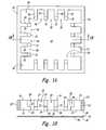
- FIG. 1Ais a front elevational view of a subassembly in accordance with one embodiment of the invention including a lead frame and a support.
- FIG. 1Bis a schematic cross-sectional view taken along line 1 B— 1 B in FIG. 1 A.
- FIG. 2Ais a front elevational view of a die received in the subassembly shown in FIG. 1 A.
- FIG. 2Bis a cross-sectional view taken along line 2 B— 2 B of FIG. 2 A.
- FIG. 3Ais a front elevational view of the subassembly of FIG. 2A wherein the die is wire bonded to the lead frame.
- FIG. 3Bis a cross-sectional view taken along line 3 B— 3 B of FIG. 3 A.
- FIGS. 4-6are successive cross-sectional views illustrating the addition of an encapsulant to the structure of FIG. 3 .
- FIG. 7Ais a front elevational view of an assembled microelectronic device assembly in accordance with an embodiment of the invention.
- FIG. 7Bis a cross-sectional view taken along line 7 B— 7 B of FIG. 7 A.
- FIG. 7Cis an edge elevational view taken along line 7 C— 7 C of FIG. 7 A.
- FIG. 8is a schematic cross-sectional view illustrating a stacked microelectronic device assembly in accordance with a further embodiment of the invention.
- FIG. 9is a front elevational view of a lead frame array in accordance with another embodiment of the invention.
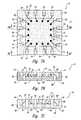
- FIG. 10Ais a front elevational view of a microelectronic device assembly in accordance with an alternative embodiment of the invention.
- FIG. 10Bis a cross-sectional view taken along line 10 B— 10 B of FIG. 10 A.
- FIG. 10Cis an edge elevational view taken alone line 10 C— 10 C of FIG. 10 A.
- FIG. 10Dis a back elevational view of the microelectronic device assembly of FIG. 10 A.
- FIG. 11is an isolation view schematically illustrating a portion of the microelectronic device assembly of FIG. 10A in greater detail.
- FIGS. 1-7schematically illustrate successive stages in manufacturing a microelectronic device assembly in accordance with one embodiment of the invention.
- FIGS. 1A-1Billustrate a first stage in assembling the microelectronic device assembly 10 of FIGS. 7A-C in accordance with one method of the invention.
- a lead frame 20is juxtaposed with a support 40 .
- the lead frame 20generally includes a peripheral dam 22 , a front surface 24 and a back surface 26 .
- the peripheral dam 22may extend generally vertically from the back surface 26 to the front surface 24 .
- a plurality of lead fingers 30may extend inwardly of the peripheral dam 22 .
- Each of the lead fingers 30may have a height equal to the height of the lead frame 20 .
- a front contact 34 of each lead finger 30may be aligned with the front surface 24 of the rest of the lead frame 20 and a back contact 36 of each lead finger 30 may be aligned with the rest of the back surface 26 of the lead frame 20 .
- Each of the lead fingers 30should be adapted to be electrically coupled to a die 60 . If the die 60 is to be electrically coupled to the lead fingers 30 by conventional wire bonding, each of the lead fingers 30 may include a bond pad 32 to provide a convenient area for connection to the bonding wire ( 75 in FIGS. 7 A-C). The lead fingers 30 are spaced from one another to define a series of gaps 38 therebetween.
- the opening 28extends through the entire thickness of the lead frame 20 , i.e., from the front surface 24 to the back surface 26 of the lead frame 20 .
- the lead framemay be formed of any suitable conductive material.
- the lead framewill be formed of a metal, with at least a portion of the lead frame plated with a noble metal such as gold, silver, or palladium.
- the support 40is adapted to sealingly yet releasably engage a surface of the lead frame 20 .
- the support 40includes a front surface 42 and a back surface 44 .
- the front surface 42is adapted to seal against the back surface 26 of the lead frame 20 .
- the support 40comprises a flexible polymeric tape which may adhere to the back surface 26 of the lead frame 20 .
- the support 40may be formed of a flexible thermoplastic material and be releasably bonded directly to the lead frame 20 by heating.
- the supportmay include a contact adhesive on the front surface 42 .
- the contact adhesive and the body of the support 40should be formed of materials which are capable of withstanding high temperatures or other conditions which may be encountered in manufacturing the microelectronic device assembly 10 .
- Nitto Denko Corporationsells a thermal resist masking tape under the product designation TRM-6250 which is expected to be suitable for use as a support 40 in connection with one embodiment of the invention.
- the support 40When the support 40 is brought into contact with the back surface 26 of the lead frame 20 , it seals against the back of the peripheral dam 22 and against the back contact 36 of each of the lead fingers 30 . This will create a seal along the lower edge of the inner periphery 27 of the opening 28 in the lead frame 20 and leave an exposed surface 46 of the support 40 spanning the opening 28 .
- a die 60may be positioned within the opening 28 in the lead frame 20 .
- the die 60may include a front surface 64 , a back surface 66 , and periphery 62 extending between the front surface 64 and the back surface 66 .
- a plurality of terminals 70may be arranged on the front surface 64 of the die in a terminal array. In the illustrated embodiment, these terminals 70 are arranged adjacent the periphery 62 of the die 60 . It should be understood, though, that other arrangements could be employed, such as a conventional lead-on chip die having a series of terminals arranged along a center line of the die 60 .
- the back surface 66 of the diemay be releasably attached to the exposed surface 46 of the support 40 within the opening 28 of the lead frame 20 .
- the support 40may temporarily hold the die 60 in a predetermined relationship with respect to the lead frame 20 to facilitate electrical coupling of the die 60 to the lead frame 20 .
- the die 60is positioned with its periphery 62 spaced inwardly of the inner periphery 27 of the opening 28 . This will define a peripheral gap 63 between the periphery 62 of the die 60 and the inner periphery 27 of the lead frame 20 .
- the order in which the lead frame 20 and die 60 are attached to the support 40can be varied. In one embodiment of the invention, the lead frame 20 is attached to the support 40 and the die 60 is then attached to the exposed surface 46 of the support 40 within the opening 28 of the lead frame 20 . In an alternative embodiment, the die 60 is first attached to the support 40 and the lead frame 20 is then attached to the support 40 . In another embodiment, the lead frame 20 and the die 60 may be simultaneously attached to the support 40 .
- each of a plurality of bonding wires 75may be coupled at one end to a terminal 70 of the die 60 and at the other end to a bond pad 32 of one of the lead fingers 30 .
- the bonding wires 75desirably have a loop height which extends no farther outwardly from the front face 64 of the die 60 than the front face 24 of the lead frame 20 .
- the bonding wires 75may be spaced behind the upper surface 24 of the lead frame 20 to facilitate complete encapsulation of the bonding wires 75 by the encapsulant 80 .
- an encapsulant 80may be delivered to the opening 28 in the lead frame 20 , as shown in FIG. 4 .
- the exposed surface 46 of the support, the inner periphery 27 of the lead frame 20 , and the die 60define a cavity which may be partially or completely filled with the encapsulant 80 .
- the peripheral gap 63 between the die 60 and the lead frame 20is completely filled. The sealing attachment of the support 40 to the lead frame 20 and the die 60 helps prevent the encapsulant 80 from flowing over the back contacts 36 of the lead fingers 30 or the back surface 66 of the die 60 .
- any suitable encapsulant 80may be used.
- the encapsulant 80can be delivered as a flowable material and subsequently cured, such as by heat treatment, UV exposure, or any combination of heating and UV exposure.
- suitable epoxy resins and other non-conductive flowable materialsare widely commercial available.
- the encapsulant 80is delivered to the opening 28 in the lead frame 20 and is allowed to simply fill the cavity noted above, covering the bonding wires 75 . If any encapsulant 80 flows outwardly over the front surface 24 of the lead frame 20 , the excess encapsulant may be removed, such as by grinding or polishing or with a solvent. In an alternative embodiment of the invention, however, flow of the encapsulant material 80 is limited by use of a front molding element 82 . This front molding element may have a substantially flat molding face 81 which may lie substantially flush against the front surface 24 of the lead frame 20 .
- any encapsulant 80does flow onto the front contacts 34 even with the use of the molding element 82 , any excess encapsulant 80 on the front contacts 34 can be removed with solvents, by grinding or polishing, or other suitable techniques.
- any front molding element 82 which is usedcan be removed.
- the support 40can also be removed from the back surface 26 of the lead frame 20 and the back surface 66 of the die 60 . As schematically shown in FIG. 5 , this may be accomplished simply by peeling the support 40 away from the rest of the structure. If any adhesive material from the support 40 remains when the support 40 is peeled away, such excess adhesive may be cleaned away using an appropriate solvent which is compatible with the lead frame 20 , the die 60 and the encapsulant 80 .
- the encapsulant 80 which is produced in this processmay have a front surface 84 which is substantially co-planar with the front surface 24 of the lead frame 20 and the front contacts 34 of each of the lead fingers 30 .
- a back surface 86 of the encapsulant 80may be substantially co-planar with the back surface 66 of the die 60 , the back contacts 36 of the lead fingers 30 and the back surface 26 of the lead frame 20 . This yields a mechanically stable structure wherein each of the lead fingers 30 defines an electrical pathway between an exposed back contact 36 and an exposed front contact 34 . As explained below, this can facilitate stacking of the microelectronic device assemblies 10 .
- the exposed back surface 66 of the die 60also helps facilitate cooling of the die 60 .
- the back surface of the dierests on a paddle and any heat generated in the die must be transferred through an adhesive to the paddle and then to the ambient environment or any attached heat sink.
- the die 60has a direct communication with a cooling medium, such as an ambient environment. If so desired, one can also attach a suitable heat sink (not shown) directly to the back surface of the die, minimizing the unnecessary thermal mass between the die 60 and the heat sink found in QFN packages.
- the peripheral dam 22physically connects each of the lead fingers 30 to one another. While the peripheral dam 22 helps define the cavity for receiving the encapsulant 80 , once the encapsulant 80 is in place, this peripheral dam can be detached from the lead fingers 30 .
- the peripheral dam 22may be separated from the lead fingers 30 in any suitable fashion, such as by cutting the peripheral dam 22 , an outer length of the lead fingers 30 , or both the peripheral dam 22 and a portion of the lead fingers 30 .
- the lead frame 20is cut within the periphery of the peripheral dam 22 using a conventional wafer saw, high-pressure water jets, lasers, or the like.
- FIGS. 3A-Bschematically illustrate a saw path S which a saw blade other cutting implement may follow in cutting one side of the lead frame 20 .
- separating the peripheral dam 22will yield a series of electrically isolated lead fingers 30 which are spaced about a periphery of the microelectronic device assembly 10 .
- the front contacts 34are peripherally aligned around the periphery of the front surface 84 of the encapsulant 80 and the back contacts 36 of the lead fingers 30 are peripherally aligned about the back surface 86 of the encapsulant 80 .
- the lead fingers 30are connected to one another only by the encapsulant 80 and the bonding wires 75 via the die 60 .
- the bonding wires 75are thin and relatively fragile and provide little structural support.
- the encapsulant 80is the primary structural element supporting the lead fingers 30 with respect to one another and with respect to the die 60 .
- the encapsulant 80can surround at least three surfaces of the body of each lead finger 30 . This helps promote a strong structural bond between the encapsulant 80 and the lead fingers 30 .
- the presence of the encapsulant 80 in the gaps 38also helps support the lead fingers 30 as the lead fingers 30 are cut from the peripheral dam 22 with a saw.
- lead fingers 30may have tapered or chamfered profiles, with each lead finger 30 tapering outwardly to a larger dimension in a direction away from the periphery of the microelectronic device assembly 10 or away from the back face 86 of the encapsulant.
- Such shapescan lead to a dovetail-like fit between the lead fingers 30 and the encapsulant 80 , further enhancing the mechanical link between the lead frames 30 and the encapsulant.
- the lead fingers 30extend the full height of the microelectronic device assembly 10 , with their front surfaces defining front contacts 34 and their back surfaces defining back contacts 36 . This simple design permits the total height to reduced because there is no need to form separate vias and contact pads.
- FIG. 8illustrates one possible application of a microelectronic device assembly 10 of FIGS. 7A-C .
- FIG. 8illustrates a stacked microelectronic device assembly wherein a pair of microelectronic device assemblies 10 such as the one shown in FIGS. 7A-C may serve as microelectronic subassemblies.
- a first subassembly 10 aincludes a die 60 a and a plurality of lead fingers 30 a , each of which has a back contact 36 a and a front contact 34 a .
- the back contact 36 a of some or all of the lead fingers 30 amay be electrically coupled to the substrate 90 in any conventional fashion.
- the lead fingers 30 acan be coupled to the substrate 90 using solder balls, reflowed connections, or other connections employed in flip chip technologies or in attaching QFN packages to substrates.
- an underfill material 91may fill the standoff gap between the lower microelectronic subassembly 10 a and the mounting surface 93 of the substrate 90 .
- the outer microelectronic device subassembly 10 balso includes a plurality of lead fingers 30 b disposed about a die 60 b .
- Each of the lead fingers 30 bincludes a front contact 34 b and a back contact 36 b .
- One or more of the lead fingers 30 b of the upper subassembly 10 bmay be electrically coupled to one or more lead fingers 30 a of the lower subassembly 10 a .
- each of the upper lead fingers 30 bis electrically coupled to one of the lower lead fingers 30 a by an electrical connector 96 .
- the electrical connectors 96may also physically bond the upper subassembly 10 b to the lower subassembly 10 a .
- These electrical connectors 96may, for example, comprise solder connections which are reflowed as is known in the art.
- the electrical connector 96has a thickness which spaces the first and second subassemblies 10 a-b from one another, defining an intercomponent gap 94 therebetween. If so desired, this intercomponent gap 94 can be filled with an underfill material or the like. This is not believed to be necessary, though, and leaving the intercomponent gap 94 exposed to the ambient environment may further facilitate cooling of the die 60 b via its exposed back surface 66 .
- An outer covering 98 of an electrically insulative materialmay be applied over the front contacts 36 b of the upper subassembly 10 b to avoid any inadvertent electrical short circuits.
- a third microelectronic device(which may be another microelectronic device assembly 10 such as that shown in FIGS. 7A-C ) may be stacked on top of the second subassembly 10 b and electrically connected thereto via the front contacts 34 b.
- FIGS. 1-8illustrate a lead frame 20 having a single opening 28 for receiving a single die 60 therein.
- the microelectronic device assemblies 10need not be assembled individually, though.
- a lead frame array 20 ′may include a plurality of individual lead frames 20 , each of which has a separate opening 28 for receiving a die (not shown). While the array 20 ′ of FIG. 9 shows twenty-five lead frames 20 arranged in a regular array, any suitable number of lead frames 20 can be formed in a single array 20 ′. If so desired, all of the lead frames 20 may be arranged in a single elongated strip rather than arranged in a grid as shown in FIG. 9 .
- FIGS. 10 and 11schematically illustrate a microelectronic device assembly 110 in accordance with an alternative embodiment of the invention.
- the encapsulant 80has been omitted in the schematic view of FIG. 11 for purposes of clarity.
- the structure of the microelectronic device assembly 110 of FIGS. 10A-Dis analogous to the structure of the microelectronic device assembly 10 of FIGS. 7A-C .
- the microelectronic device assembly 110includes a die 160 having a periphery 162 and a plurality of terminals 170 carried on a front surface 164 of the die 160 .
- the die 160may be electrically coupled to a plurality of lead fingers 130 a-b by a plurality of bonding wires 175 .
- the back surface 166 of the die 160may remain exposed and be substantially coplanar with the back surface 186 of the encapsulant 180 .
- the microelectronic device assemblyalso includes a plurality of lead fingers 130 which are electrically coupled to the die 160 by a plurality of bonding wires 175 .
- One of the distinctions between the microelectronic device assembly 110 of FIGS. 10 and 11 and the microelectronic device assembly 10 of FIGS. 7A-Crelates to the shape and arrangement of the lead fingers 130 .
- all of the lead fingers 30were generally L-shaped and both the front contacts 34 and the back contacts 36 were peripherally aligned on the front surface 84 or the back surface 86 , respectively, of the encapsulant 80 .
- FIGS. 7A-Call of the lead fingers 30 were generally L-shaped and both the front contacts 34 and the back contacts 36 were peripherally aligned on the front surface 84 or the back surface 86 , respectively, of the encapsulant 80 .
- the microelectronic device assembly 110includes a plurality of first lead fingers 130 a and a plurality of second lead fingers 130 b .
- the first lead fingers 130 aare spaced a first distance D 1 from the periphery 162 of the die 160 and the second lead fingers 130 b are spaced a greater second distance D 2 from the periphery 162 of the die 160 .
- the first lead fingers 130 aall have the same first shape and the second lead fingers 130 b all have the same second shape, but the first shape of the first lead fingers 130 a is different from the second shape of the second lead fingers 130 b .
- the second lead fingers 130 bmay be generally L-shaped having a bond pad 132 b for connection to the bonding wires 175 . This positions the front contact 134 and the back contact 136 adjacent the periphery of the microelectronic device assembly 110 .
- the front contacts 134 b of the second lead fingers 130 bare aligned with the front encapsulant surface 184 and may be peripherally aligned on the front encapsulant surface 184 .
- the back contacts 136 b of the second lead fingers 130 bmay be exposed and peripherally aligned on the back encapsulant surface 186 .
- the shape and orientation of the second lead fingers 130 bis directly analogous to that of the lead fingers 30 in the microelectronic device assembly 10 of FIGS. 7A-C .
- the first lead fingers 130 a of FIGS. 10 and 11may be generally Z-shaped.
- the front contact 134 amay extend inwardly from the periphery of the microelectronic device assembly 110 a predetermined distance.
- This front contact 134 amay be longer than the front contact 134 b of the second lead fingers 130 b .
- the back contact 136 a of the lead, fingers 130 ais spaced inwardly from the periphery of the microelectronic device assembly 110 by a predetermined offset O.
- This back contact 136 amay be positioned beneath the bond pad 132 a of the lead finger 130 a.
- each of the front contacts 134 a-bmay be peripherally aligned and coplanar with the front surface 184 of the encapsulant 180 .
- the first front contacts 134 amay extend inwardly toward the die 160 farther than the second front contacts 134 b .
- each of the second back contacts 136 bare peripherally aligned and coplanar with the back surface 186 of the encapsulant 180 .
- Each of the first back contacts 136 ais spaced inwardly from the periphery of the microelectronic device assembly 110 by the predetermined offset O, though.
- first and second back contacts 136 a-bdefine a staggered array of back contacts 136 which are exposed on the back surface 186 of the encapsulant 180 .
- This staggered array configurationprovides a material improvement over the limited QFN package design.
- QFN packagesare conventionally limited to leads positioned at the periphery of the bottom surface of the package.
- the microelectronic device assembly 110 of FIGS. 10 and 11may be used in conventional ball-grid array or fine ball-grid array manufacturing processes, expanding their utility into other existing applications.
- the microelectronic device assembly 110 of FIGS. 10 and 11may also be stacked one on top of the other in a manner directly analogous to the structure shown in FIG. 8 .
- the first front contacts 134 aextend inwardly from the periphery of the device. This permits the first front contact 134 a of a lower assembly 110 to be positioned beneath the inwardly offset first back contact 136 a of an upper assembly 110 .
- QFN packagescannot be stacked, as explained previously.
- the microelectronic device assembly 110 of FIGS. 10 and 11may be manufactured in a process directly analogous to that discussed above in connection with FIGS. 7A-C .
- each of the lead fingers 130 a-bmay be carried on a lead frame much like the lead frame 20 of FIGS. 1-6 .
- a support( 40 in FIG. 10B ) may sealingly engage a lower surface of the lead frame, including the first and second back contacts 136 a-b of the lead fingers 130 a-b .
- the opening in the lead framemay then be filled with the encapsulant 180 and the peripheral dam of the lead frame may be cut away, leaving the structure shown in FIGS. 10A-B .
- FIG. 10Billustrates in dashed lines the position of the support 40 during manufacture to illustrate the relationship of the support 40 to the lead fingers 130 a-b .
- the back contact 136 b of the second lead fingers 130 bextends inwardly from the periphery of the assembly 110 .
- the support 40may sealingly engage the second back contact 136 and preclude any encapsulant 180 from passing between the support 40 and the second lead finger 130 b .
- the back contact 136 a of the first lead finger 130 ais offset from the periphery of the assembly 110 . Over the length of this offset O, the first lead finger 130 a is spaced above the front surface 42 of the support 40 .
- the encapsulant 180is permitted to flow between the support 40 and a length of each of the first lead fingers 130 a beneath the first front contacts 134 a .
Landscapes
- Engineering & Computer Science (AREA)
- Power Engineering (AREA)
- Microelectronics & Electronic Packaging (AREA)
- Computer Hardware Design (AREA)
- Physics & Mathematics (AREA)
- Condensed Matter Physics & Semiconductors (AREA)
- General Physics & Mathematics (AREA)
- Manufacturing & Machinery (AREA)
- Encapsulation Of And Coatings For Semiconductor Or Solid State Devices (AREA)
- Lead Frames For Integrated Circuits (AREA)
Abstract
Description
Claims (15)
Priority Applications (1)
| Application Number | Priority Date | Filing Date | Title |
|---|---|---|---|
| US10/929,613US6943450B2 (en) | 2001-08-29 | 2004-08-30 | Packaged microelectronic devices and methods of forming same |
Applications Claiming Priority (5)
| Application Number | Priority Date | Filing Date | Title |
|---|---|---|---|
| SG200105297ASG111919A1 (en) | 2001-08-29 | 2001-08-29 | Packaged microelectronic devices and methods of forming same |
| SG200105297-6 | 2001-08-29 | ||
| SG200105297 | 2001-08-29 | ||
| US09/944,246US6876066B2 (en) | 2001-08-29 | 2001-08-30 | Packaged microelectronic devices and methods of forming same |
| US10/929,613US6943450B2 (en) | 2001-08-29 | 2004-08-30 | Packaged microelectronic devices and methods of forming same |
Related Parent Applications (1)
| Application Number | Title | Priority Date | Filing Date |
|---|---|---|---|
| US09/944,246DivisionUS6876066B2 (en) | 2001-08-29 | 2001-08-30 | Packaged microelectronic devices and methods of forming same |
Publications (2)
| Publication Number | Publication Date |
|---|---|
| US20050023655A1 US20050023655A1 (en) | 2005-02-03 |
| US6943450B2true US6943450B2 (en) | 2005-09-13 |
Family
ID=20430824
Family Applications (2)
| Application Number | Title | Priority Date | Filing Date |
|---|---|---|---|
| US09/944,246Expired - LifetimeUS6876066B2 (en) | 2001-08-29 | 2001-08-30 | Packaged microelectronic devices and methods of forming same |
| US10/929,613Expired - LifetimeUS6943450B2 (en) | 2001-08-29 | 2004-08-30 | Packaged microelectronic devices and methods of forming same |
Family Applications Before (1)
| Application Number | Title | Priority Date | Filing Date |
|---|---|---|---|
| US09/944,246Expired - LifetimeUS6876066B2 (en) | 2001-08-29 | 2001-08-30 | Packaged microelectronic devices and methods of forming same |
Country Status (2)
| Country | Link |
|---|---|
| US (2) | US6876066B2 (en) |
| SG (1) | SG111919A1 (en) |
Cited By (42)
| Publication number | Priority date | Publication date | Assignee | Title |
|---|---|---|---|---|
| US20060202319A1 (en)* | 2004-08-19 | 2006-09-14 | Swee Seng Eric T | Assemblies and multi-chip modules including stacked semiconductor dice having centrally located, wire bonded bond pads |
| US20070013038A1 (en)* | 2005-07-13 | 2007-01-18 | Advanced Semiconductor Engineering, Inc. | Semiconductor package having pre-plated leads and method of manufacturing the same |
| US20070135055A1 (en)* | 2005-12-13 | 2007-06-14 | Ho Lee S | Combination quad flat no-lead and thin small outline package |
| US20070158858A1 (en)* | 2006-01-11 | 2007-07-12 | Stats Chippac Ltd. | Inter-stacking module system |
| US7276790B2 (en) | 2004-07-29 | 2007-10-02 | Micron Technology, Inc. | Methods of forming a multi-chip module having discrete spacers |
| US20070246810A1 (en)* | 2005-09-20 | 2007-10-25 | United Test And Assembly Test Center Ltd. | Leadframe enhancement and method of producing a multi-row semiconductor package |
| US7379316B2 (en) | 2005-09-02 | 2008-05-27 | Metaram, Inc. | Methods and apparatus of stacking DRAMs |
| US7515453B2 (en) | 2005-06-24 | 2009-04-07 | Metaram, Inc. | Integrated memory core and memory interface circuit |
| US20090091009A1 (en)* | 2007-10-03 | 2009-04-09 | Corisis David J | Stackable integrated circuit package |
| US20090200074A1 (en)* | 2008-02-12 | 2009-08-13 | International Business Machines Corporation | Circuit Substrate Having Post-Fed Die Side Power Supply Connections |
| US7671459B2 (en) | 2006-02-08 | 2010-03-02 | Micron Technologies, Inc. | Microelectronic devices, stacked microelectronic devices, and methods for manufacturing such devices |
| US20110059582A1 (en)* | 2008-08-28 | 2011-03-10 | Yong Liu | Molded ultra thin semiconductor die packages, systems using the same, and methods of making the same |
| US8019589B2 (en) | 2006-07-31 | 2011-09-13 | Google Inc. | Memory apparatus operable to perform a power-saving operation |
| US8055833B2 (en) | 2006-10-05 | 2011-11-08 | Google Inc. | System and method for increasing capacity, performance, and flexibility of flash storage |
| US8060774B2 (en) | 2005-06-24 | 2011-11-15 | Google Inc. | Memory systems and memory modules |
| US8081474B1 (en) | 2007-12-18 | 2011-12-20 | Google Inc. | Embossed heat spreader |
| US8080874B1 (en) | 2007-09-14 | 2011-12-20 | Google Inc. | Providing additional space between an integrated circuit and a circuit board for positioning a component therebetween |
| US8089795B2 (en) | 2006-02-09 | 2012-01-03 | Google Inc. | Memory module with memory stack and interface with enhanced capabilities |
| US8090897B2 (en) | 2006-07-31 | 2012-01-03 | Google Inc. | System and method for simulating an aspect of a memory circuit |
| US8111566B1 (en) | 2007-11-16 | 2012-02-07 | Google, Inc. | Optimal channel design for memory devices for providing a high-speed memory interface |
| US8122207B2 (en) | 2006-07-31 | 2012-02-21 | Google Inc. | Apparatus and method for power management of memory circuits by a system or component thereof |
| US8130560B1 (en) | 2006-11-13 | 2012-03-06 | Google Inc. | Multi-rank partial width memory modules |
| US8154935B2 (en) | 2006-07-31 | 2012-04-10 | Google Inc. | Delaying a signal communicated from a system to at least one of a plurality of memory circuits |
| US8169233B2 (en) | 2009-06-09 | 2012-05-01 | Google Inc. | Programming of DIMM termination resistance values |
| US8181048B2 (en) | 2006-07-31 | 2012-05-15 | Google Inc. | Performing power management operations |
| US8209479B2 (en) | 2007-07-18 | 2012-06-26 | Google Inc. | Memory circuit system and method |
| US8244971B2 (en) | 2006-07-31 | 2012-08-14 | Google Inc. | Memory circuit system and method |
| US8280714B2 (en) | 2006-07-31 | 2012-10-02 | Google Inc. | Memory circuit simulation system and method with refresh capabilities |
| US8327104B2 (en) | 2006-07-31 | 2012-12-04 | Google Inc. | Adjusting the timing of signals associated with a memory system |
| US8335894B1 (en) | 2008-07-25 | 2012-12-18 | Google Inc. | Configurable memory system with interface circuit |
| US8386722B1 (en) | 2008-06-23 | 2013-02-26 | Google Inc. | Stacked DIMM memory interface |
| US8397013B1 (en) | 2006-10-05 | 2013-03-12 | Google Inc. | Hybrid memory module |
| US8438328B2 (en) | 2008-02-21 | 2013-05-07 | Google Inc. | Emulation of abstracted DIMMs using abstracted DRAMs |
| US8566516B2 (en) | 2006-07-31 | 2013-10-22 | Google Inc. | Refresh management of memory modules |
| US8773937B2 (en) | 2005-06-24 | 2014-07-08 | Google Inc. | Memory refresh apparatus and method |
| US8796830B1 (en) | 2006-09-01 | 2014-08-05 | Google Inc. | Stackable low-profile lead frame package |
| US8949519B2 (en) | 2005-06-24 | 2015-02-03 | Google Inc. | Simulating a memory circuit |
| US9171585B2 (en) | 2005-06-24 | 2015-10-27 | Google Inc. | Configurable memory circuit system and method |
| US9507739B2 (en) | 2005-06-24 | 2016-11-29 | Google Inc. | Configurable memory circuit system and method |
| US9542352B2 (en) | 2006-02-09 | 2017-01-10 | Google Inc. | System and method for reducing command scheduling constraints of memory circuits |
| US9632929B2 (en) | 2006-02-09 | 2017-04-25 | Google Inc. | Translating an address associated with a command communicated between a system and memory circuits |
| US10013371B2 (en) | 2005-06-24 | 2018-07-03 | Google Llc | Configurable memory circuit system and method |
Families Citing this family (72)
| Publication number | Priority date | Publication date | Assignee | Title |
|---|---|---|---|---|
| US6576494B1 (en) | 2000-06-28 | 2003-06-10 | Micron Technology, Inc. | Recessed encapsulated microelectronic devices and methods for formation |
| JP2002184934A (en)* | 2000-12-13 | 2002-06-28 | Shinko Electric Ind Co Ltd | Semiconductor device and manufacturing method thereof |
| SG111919A1 (en)* | 2001-08-29 | 2005-06-29 | Micron Technology Inc | Packaged microelectronic devices and methods of forming same |
| TW533566B (en)* | 2002-01-31 | 2003-05-21 | Siliconware Precision Industries Co Ltd | Short-prevented lead frame and method for fabricating semiconductor package with the same |
| US6769174B2 (en)* | 2002-07-26 | 2004-08-03 | Stmicroeletronics, Inc. | Leadframeless package structure and method |
| SG120879A1 (en)* | 2002-08-08 | 2006-04-26 | Micron Technology Inc | Packaged microelectronic components |
| SG114585A1 (en)* | 2002-11-22 | 2005-09-28 | Micron Technology Inc | Packaged microelectronic component assemblies |
| EP1597762A4 (en)* | 2003-02-04 | 2007-07-04 | Advanced Interconnect Tech Ltd | Thin multiple semiconductor die package |
| US7405468B2 (en)* | 2003-04-11 | 2008-07-29 | Dai Nippon Printing Co., Ltd. | Plastic package and method of fabricating the same |
| CN101587869B (en)* | 2003-08-26 | 2011-04-13 | 宇芯(毛里求斯)控股有限公司 | Reversible leadless package and methods of making and using same |
| US7368810B2 (en)* | 2003-08-29 | 2008-05-06 | Micron Technology, Inc. | Invertible microfeature device packages |
| TWI228303B (en)* | 2003-10-29 | 2005-02-21 | Advanced Semiconductor Eng | Semiconductor package, method for manufacturing the same and lead frame for use in the same |
| JP4383274B2 (en)* | 2004-06-30 | 2009-12-16 | Necエレクトロニクス株式会社 | Semiconductor device and semiconductor wafer manufacturing method |
| US7498666B2 (en)* | 2004-09-27 | 2009-03-03 | Nokia Corporation | Stacked integrated circuit |
| US20070004093A1 (en)* | 2004-10-07 | 2007-01-04 | Optimum Care International Tech. Inc. | Method of fabricating a high-density lead arrangement package structure |
| US7256479B2 (en)* | 2005-01-13 | 2007-08-14 | Fairchild Semiconductor Corporation | Method to manufacture a universal footprint for a package with exposed chip |
| US7375415B2 (en)* | 2005-06-30 | 2008-05-20 | Sandisk Corporation | Die package with asymmetric leadframe connection |
| US20070045807A1 (en)* | 2005-09-01 | 2007-03-01 | Micron Technology, Inc. | Microelectronic devices and methods for manufacturing microelectronic devices |
| US7943431B2 (en)* | 2005-12-02 | 2011-05-17 | Unisem (Mauritius) Holdings Limited | Leadless semiconductor package and method of manufacture |
| TW200729444A (en)* | 2006-01-16 | 2007-08-01 | Siliconware Precision Industries Co Ltd | Semiconductor package structure and fabrication method thereof |
| DE112006003664B4 (en)* | 2006-02-01 | 2011-09-08 | Infineon Technologies Ag | Making a QFN package for an integrated circuit and QFN package made using it, and using a leadframe |
| US7863737B2 (en)* | 2006-04-01 | 2011-01-04 | Stats Chippac Ltd. | Integrated circuit package system with wire bond pattern |
| US8487451B2 (en)* | 2006-04-28 | 2013-07-16 | Utac Thai Limited | Lead frame land grid array with routing connector trace under unit |
| US8492906B2 (en)* | 2006-04-28 | 2013-07-23 | Utac Thai Limited | Lead frame ball grid array with traces under die |
| US8310060B1 (en) | 2006-04-28 | 2012-11-13 | Utac Thai Limited | Lead frame land grid array |
| US8461694B1 (en) | 2006-04-28 | 2013-06-11 | Utac Thai Limited | Lead frame ball grid array with traces under die having interlocking features |
| US8460970B1 (en) | 2006-04-28 | 2013-06-11 | Utac Thai Limited | Lead frame ball grid array with traces under die having interlocking features |
| JP2007324354A (en)* | 2006-05-31 | 2007-12-13 | Sony Corp | Semiconductor device |
| DE102006037538B4 (en)* | 2006-08-10 | 2016-03-10 | Infineon Technologies Ag | Electronic component, electronic component stack and method for their production and use of a bead placement machine for carrying out a method for producing an electronic component or component stack |
| US8013437B1 (en) | 2006-09-26 | 2011-09-06 | Utac Thai Limited | Package with heat transfer |
| US8125077B2 (en)* | 2006-09-26 | 2012-02-28 | Utac Thai Limited | Package with heat transfer |
| SG143098A1 (en) | 2006-12-04 | 2008-06-27 | Micron Technology Inc | Packaged microelectronic devices and methods for manufacturing packaged microelectronic devices |
| US9082607B1 (en) | 2006-12-14 | 2015-07-14 | Utac Thai Limited | Molded leadframe substrate semiconductor package |
| US9761435B1 (en) | 2006-12-14 | 2017-09-12 | Utac Thai Limited | Flip chip cavity package |
| US20080182434A1 (en)* | 2007-01-25 | 2008-07-31 | Analog Devices, Inc. | Low Cost Stacked Package |
| US7884457B2 (en)* | 2007-06-26 | 2011-02-08 | Stats Chippac Ltd. | Integrated circuit package system with dual side connection |
| US7893545B2 (en)* | 2007-07-18 | 2011-02-22 | Infineon Technologies Ag | Semiconductor device |
| US7790512B1 (en) | 2007-11-06 | 2010-09-07 | Utac Thai Limited | Molded leadframe substrate semiconductor package |
| KR101472900B1 (en)* | 2007-12-06 | 2014-12-15 | 페어차일드코리아반도체 주식회사 | Molded leadless package and methods of fabricating the same |
| US8063470B1 (en)* | 2008-05-22 | 2011-11-22 | Utac Thai Limited | Method and apparatus for no lead semiconductor package |
| US8227908B2 (en)* | 2008-07-07 | 2012-07-24 | Infineon Technologies Ag | Electronic device having contact elements with a specified cross section and manufacturing thereof |
| US9947605B2 (en)* | 2008-09-04 | 2018-04-17 | UTAC Headquarters Pte. Ltd. | Flip chip cavity package |
| US7829988B2 (en)* | 2008-09-22 | 2010-11-09 | Fairchild Semiconductor Corporation | Stacking quad pre-molded component packages, systems using the same, and methods of making the same |
| US8314499B2 (en)* | 2008-11-14 | 2012-11-20 | Fairchild Semiconductor Corporation | Flexible and stackable semiconductor die packages having thin patterned conductive layers |
| US9064936B2 (en)* | 2008-12-12 | 2015-06-23 | Stats Chippac, Ltd. | Semiconductor device and method of forming a vertical interconnect structure for 3-D FO-WLCSP |
| US9293401B2 (en) | 2008-12-12 | 2016-03-22 | Stats Chippac, Ltd. | Semiconductor device and method for forming a low profile embedded wafer level ball grid array molded laser package (EWLP-MLP) |
| US9082806B2 (en) | 2008-12-12 | 2015-07-14 | Stats Chippac, Ltd. | Semiconductor device and method of forming a vertical interconnect structure for 3-D FO-WLCSP |
| US8569877B2 (en)* | 2009-03-12 | 2013-10-29 | Utac Thai Limited | Metallic solderability preservation coating on metal part of semiconductor package to prevent oxide |
| US9449900B2 (en)* | 2009-07-23 | 2016-09-20 | UTAC Headquarters Pte. Ltd. | Leadframe feature to minimize flip-chip semiconductor die collapse during flip-chip reflow |
| US9355940B1 (en) | 2009-12-04 | 2016-05-31 | Utac Thai Limited | Auxiliary leadframe member for stabilizing the bond wire process |
| US8368189B2 (en)* | 2009-12-04 | 2013-02-05 | Utac Thai Limited | Auxiliary leadframe member for stabilizing the bond wire process |
| US8193620B2 (en)* | 2010-02-17 | 2012-06-05 | Analog Devices, Inc. | Integrated circuit package with enlarged die paddle |
| US8575732B2 (en) | 2010-03-11 | 2013-11-05 | Utac Thai Limited | Leadframe based multi terminal IC package |
| US8871571B2 (en) | 2010-04-02 | 2014-10-28 | Utac Thai Limited | Apparatus for and methods of attaching heat slugs to package tops |
| US8558369B2 (en)* | 2011-03-25 | 2013-10-15 | Stats Chippac Ltd. | Integrated circuit packaging system with interconnects and method of manufacture thereof |
| US20120326324A1 (en)* | 2011-06-22 | 2012-12-27 | Lee Hyungmin | Integrated circuit packaging system with package stacking and method of manufacture thereof |
| TWI455269B (en)* | 2011-07-20 | 2014-10-01 | Chipmos Technologies Inc | Chip package structure and manufacturing method thereof |
| US8916421B2 (en)* | 2011-08-31 | 2014-12-23 | Freescale Semiconductor, Inc. | Semiconductor device packaging having pre-encapsulation through via formation using lead frames with attached signal conduits |
| US9142502B2 (en)* | 2011-08-31 | 2015-09-22 | Zhiwei Gong | Semiconductor device packaging having pre-encapsulation through via formation using drop-in signal conduits |
| US8597983B2 (en) | 2011-11-18 | 2013-12-03 | Freescale Semiconductor, Inc. | Semiconductor device packaging having substrate with pre-encapsulation through via formation |
| US9029198B2 (en) | 2012-05-10 | 2015-05-12 | Utac Thai Limited | Methods of manufacturing semiconductor devices including terminals with internal routing interconnections |
| US9449905B2 (en) | 2012-05-10 | 2016-09-20 | Utac Thai Limited | Plated terminals with routing interconnections semiconductor device |
| US9006034B1 (en) | 2012-06-11 | 2015-04-14 | Utac Thai Limited | Post-mold for semiconductor package having exposed traces |
| JP6028592B2 (en) | 2013-01-25 | 2016-11-16 | 三菱電機株式会社 | Semiconductor device |
| WO2014188632A1 (en)* | 2013-05-23 | 2014-11-27 | パナソニック株式会社 | Semiconductor device having heat dissipation structure and laminate of semiconductor devices |
| US10242953B1 (en) | 2015-05-27 | 2019-03-26 | Utac Headquarters PTE. Ltd | Semiconductor package with plated metal shielding and a method thereof |
| US10242934B1 (en) | 2014-05-07 | 2019-03-26 | Utac Headquarters Pte Ltd. | Semiconductor package with full plating on contact side surfaces and methods thereof |
| CN105405823A (en)* | 2014-08-20 | 2016-03-16 | 飞思卡尔半导体公司 | Semiconductor device with inspectable solder joints |
| US9379087B2 (en)* | 2014-11-07 | 2016-06-28 | Texas Instruments Incorporated | Method of making a QFN package |
| US9917038B1 (en) | 2015-11-10 | 2018-03-13 | Utac Headquarters Pte Ltd | Semiconductor package with multiple molding routing layers and a method of manufacturing the same |
| US10276477B1 (en) | 2016-05-20 | 2019-04-30 | UTAC Headquarters Pte. Ltd. | Semiconductor package with multiple stacked leadframes and a method of manufacturing the same |
| TWI637536B (en)* | 2017-02-24 | 2018-10-01 | 矽品精密工業股份有限公司 | Electronic package structure and the manufacture thereof |
Citations (130)
| Publication number | Priority date | Publication date | Assignee | Title |
|---|---|---|---|---|
| US4012579A (en) | 1975-02-21 | 1977-03-15 | Allen-Bradley Company | Encapsulated microcircuit package and method for assembly thereof |
| US4862245A (en) | 1985-04-18 | 1989-08-29 | International Business Machines Corporation | Package semiconductor chip |
| US4996587A (en) | 1989-04-10 | 1991-02-26 | International Business Machines Corporation | Integrated semiconductor chip package |
| US5107328A (en) | 1991-02-13 | 1992-04-21 | Micron Technology, Inc. | Packaging means for a semiconductor die having particular shelf structure |
| US5128831A (en) | 1991-10-31 | 1992-07-07 | Micron Technology, Inc. | High-density electronic package comprising stacked sub-modules which are electrically interconnected by solder-filled vias |
| US5138434A (en) | 1991-01-22 | 1992-08-11 | Micron Technology, Inc. | Packaging for semiconductor logic devices |
| US5140404A (en) | 1990-10-24 | 1992-08-18 | Micron Technology, Inc. | Semiconductor device manufactured by a method for attaching a semiconductor die to a leadframe using a thermoplastic covered carrier tape |
| US5252853A (en) | 1991-09-19 | 1993-10-12 | Mitsubishi Denki Kabushiki Kaisha | Packaged semiconductor device having tab tape and particular power distribution lead structure |
| US5252857A (en) | 1991-08-05 | 1993-10-12 | International Business Machines Corporation | Stacked DCA memory chips |
| US5304842A (en) | 1990-10-24 | 1994-04-19 | Micron Technology, Inc. | Dissimilar adhesive die attach for semiconductor devices |
| US5471369A (en) | 1993-07-09 | 1995-11-28 | Fujitsu Limited | Semiconductor device having a plurality of semiconductor chips |
| US5475918A (en) | 1993-10-01 | 1995-12-19 | Electroplating Engineers Of Japan Ltd. | Method of preventing deformation of lead frames |
| US5518957A (en) | 1991-10-10 | 1996-05-21 | Samsung Electronics Co., Ltd. | Method for making a thin profile semiconductor package |
| US5536969A (en) | 1992-12-18 | 1996-07-16 | Yamaichi Electronics Co., Ltd. | IC carrier |
| US5583371A (en) | 1994-10-12 | 1996-12-10 | Kabushiki Kaisha Toshiba | Resin-sealed semiconductor device capable of improving in heat radiation characteristics of resin-sealed semiconductor elements |
| US5593927A (en) | 1993-10-14 | 1997-01-14 | Micron Technology, Inc. | Method for packaging semiconductor dice |
| US5663593A (en) | 1995-10-17 | 1997-09-02 | National Semiconductor Corporation | Ball grid array package with lead frame |
| US5665651A (en) | 1993-07-15 | 1997-09-09 | Kabushiki Kaisha Toshiba | Process for encapsulating a semiconductor device and lead frame |
| US5677566A (en) | 1995-05-08 | 1997-10-14 | Micron Technology, Inc. | Semiconductor chip package |
| US5696033A (en) | 1995-08-16 | 1997-12-09 | Micron Technology, Inc. | Method for packaging a semiconductor die |
| US5715593A (en) | 1996-01-30 | 1998-02-10 | Nec Corporation | Method of making plastic-packaged semiconductor integrated circuit |
| US5729049A (en) | 1996-03-19 | 1998-03-17 | Micron Technology, Inc. | Tape under frame for conventional-type IC package assembly |
| US5739585A (en) | 1995-11-27 | 1998-04-14 | Micron Technology, Inc. | Single piece package for semiconductor die |
| US5744827A (en) | 1995-11-28 | 1998-04-28 | Samsung Electronics Co., Ltd. | Three dimensional stack package device having exposed coupling lead portions and vertical interconnection elements |
| USD394844S (en) | 1997-04-25 | 1998-06-02 | Micron Technology, Inc. | Temporary package for semiconductor dice |
| US5815000A (en) | 1991-06-04 | 1998-09-29 | Micron Technology, Inc. | Method for testing semiconductor dice with conventionally sized temporary packages |
| US5847455A (en) | 1995-11-07 | 1998-12-08 | Vlsi Technology, Inc. | Molded leadframe ball grid array |
| USD402638S (en) | 1997-04-25 | 1998-12-15 | Micron Technology, Inc. | Temporary package for semiconductor dice |
| US5851845A (en) | 1995-12-18 | 1998-12-22 | Micron Technology, Inc. | Process for packaging a semiconductor die using dicing and testing |
| US5866939A (en) | 1996-01-21 | 1999-02-02 | Anam Semiconductor Inc. | Lead end grid array semiconductor package |
| US5866953A (en) | 1996-05-24 | 1999-02-02 | Micron Technology, Inc. | Packaged die on PCB with heat sink encapsulant |
| US5879965A (en) | 1997-06-19 | 1999-03-09 | Micron Technology, Inc. | Plastic lead frames for semiconductor devices, packages including same, and methods of fabrication |
| US5883426A (en) | 1996-04-18 | 1999-03-16 | Nec Corporation | Stack module |
| US5891753A (en) | 1997-01-24 | 1999-04-06 | Micron Technology, Inc. | Method and apparatus for packaging flip chip bare die on printed circuit boards |
| US5891797A (en) | 1997-10-20 | 1999-04-06 | Micron Technology, Inc. | Method of forming a support structure for air bridge wiring of an integrated circuit |
| US5893726A (en) | 1997-12-15 | 1999-04-13 | Micron Technology, Inc. | Semiconductor package with pre-fabricated cover and method of fabrication |
| US5933713A (en) | 1998-04-06 | 1999-08-03 | Micron Technology, Inc. | Method of forming overmolded chip scale package and resulting product |
| US5938956A (en) | 1996-09-10 | 1999-08-17 | Micron Technology, Inc. | Circuit and method for heating an adhesive to package or rework a semiconductor die |
| US5946553A (en) | 1991-06-04 | 1999-08-31 | Micron Technology, Inc. | Process for manufacturing a semiconductor package with bi-substrate die |
| US5956236A (en) | 1997-11-25 | 1999-09-21 | Micron Technology, Inc. | Integrated circuit package support system |
| US5958100A (en) | 1993-06-03 | 1999-09-28 | Micron Technology, Inc. | Process of making a glass semiconductor package |
| US5973393A (en) | 1996-12-20 | 1999-10-26 | Lsi Logic Corporation | Apparatus and method for stackable molded lead frame ball grid array packaging of integrated circuits |
| US5973396A (en) | 1996-02-16 | 1999-10-26 | Micron Technology, Inc. | Surface mount IC using silicon vias in an area array format or same size as die array |
| US5986209A (en) | 1997-07-09 | 1999-11-16 | Micron Technology, Inc. | Package stack via bottom leaded plastic (BLP) packaging |
| US5990566A (en) | 1998-05-20 | 1999-11-23 | Micron Technology, Inc. | High density semiconductor package |
| US5989941A (en) | 1997-12-12 | 1999-11-23 | Micron Technology, Inc. | Encapsulated integrated circuit packaging |
| US5994784A (en) | 1997-12-18 | 1999-11-30 | Micron Technology, Inc. | Die positioning in integrated circuit packaging |
| US6008070A (en) | 1998-05-21 | 1999-12-28 | Micron Technology, Inc. | Wafer level fabrication and assembly of chip scale packages |
| USRE36469E (en) | 1988-09-30 | 1999-12-28 | Micron Technology, Inc. | Packaging for semiconductor logic devices |
| US6020629A (en) | 1998-06-05 | 2000-02-01 | Micron Technology, Inc. | Stacked semiconductor package and method of fabrication |
| US6025728A (en) | 1997-04-25 | 2000-02-15 | Micron Technology, Inc. | Semiconductor package with wire bond protective member |
| US6028365A (en) | 1998-03-30 | 2000-02-22 | Micron Technology, Inc. | Integrated circuit package and method of fabrication |
| US6046496A (en) | 1997-11-04 | 2000-04-04 | Micron Technology Inc | Chip package |
| US6048755A (en) | 1998-11-12 | 2000-04-11 | Micron Technology, Inc. | Method for fabricating BGA package using substrate with patterned solder mask open in die attach area |
| US6049125A (en) | 1997-12-29 | 2000-04-11 | Micron Technology, Inc. | Semiconductor package with heat sink and method of fabrication |
| US6048744A (en) | 1997-09-15 | 2000-04-11 | Micron Technology, Inc. | Integrated circuit package alignment feature |
| US6051878A (en) | 1997-03-10 | 2000-04-18 | Micron Technology, Inc. | Method of constructing stacked packages |
| US6060778A (en) | 1997-05-17 | 2000-05-09 | Hyundai Electronics Industries Co. Ltd. | Ball grid array package |
| US6066514A (en) | 1996-10-18 | 2000-05-23 | Micron Technology, Inc. | Adhesion enhanced semiconductor die for mold compound packaging |
| US6072233A (en) | 1998-05-04 | 2000-06-06 | Micron Technology, Inc. | Stackable ball grid array package |
| US6072236A (en) | 1996-03-07 | 2000-06-06 | Micron Technology, Inc. | Micromachined chip scale package |
| US6075284A (en) | 1998-06-30 | 2000-06-13 | Hyundai Electronics Industries Co., Ltd. | Stack package |
| US6075288A (en) | 1998-06-08 | 2000-06-13 | Micron Technology, Inc. | Semiconductor package having interlocking heat sinks and method of fabrication |
| US6089920A (en) | 1998-05-04 | 2000-07-18 | Micron Technology, Inc. | Modular die sockets with flexible interconnects for packaging bare semiconductor die |
| US6094058A (en) | 1991-06-04 | 2000-07-25 | Micron Technology, Inc. | Temporary semiconductor package having dense array external contacts |
| US6093969A (en) | 1999-05-15 | 2000-07-25 | Lin; Paul T. | Face-to-face (FTF) stacked assembly of substrate-on-bare-chip (SOBC) modules |
| US6097087A (en) | 1997-10-31 | 2000-08-01 | Micron Technology, Inc. | Semiconductor package including flex circuit, interconnects and dense array external contacts |
| US6103547A (en) | 1997-01-17 | 2000-08-15 | Micron Technology, Inc. | High speed IC package configuration |
| US6107122A (en) | 1997-08-04 | 2000-08-22 | Micron Technology, Inc. | Direct die contact (DDC) semiconductor package |
| US6107680A (en) | 1995-01-04 | 2000-08-22 | Micron Technology, Inc. | Packaging for bare dice employing EMR-sensitive adhesives |
| US6117710A (en) | 1997-02-11 | 2000-09-12 | National Semiconductor Corporation | Plastic package with exposed die and method of making same |
| US6117382A (en) | 1998-02-05 | 2000-09-12 | Micron Technology, Inc. | Method for encasing array packages |
| US6133068A (en) | 1997-10-06 | 2000-10-17 | Micron Technology, Inc. | Increasing the gap between a lead frame and a semiconductor die |
| US6137162A (en) | 1998-05-12 | 2000-10-24 | Hyundai Electronics Industries Co., Ltd. | Chip stack package |
| US6148509A (en) | 1997-04-07 | 2000-11-21 | Micron Technology, Inc. | Method for supporting an integrated circuit die |
| US6150710A (en) | 1998-08-20 | 2000-11-21 | Micron Technology, Inc. | Transverse hybrid LOC package |
| US6153924A (en) | 1998-02-23 | 2000-11-28 | Micron Technology, Inc. | Multilayered lead frame for semiconductor package |
| US6159764A (en) | 1997-07-02 | 2000-12-12 | Micron Technology, Inc. | Varied-thickness heat sink for integrated circuit (IC) packages and method of fabricating IC packages |
| US6172419B1 (en) | 1998-02-24 | 2001-01-09 | Micron Technology, Inc. | Low profile ball grid array package |
| US6175149B1 (en) | 1998-02-13 | 2001-01-16 | Micron Technology, Inc. | Mounting multiple semiconductor dies in a package |
| US6184465B1 (en) | 1998-11-12 | 2001-02-06 | Micron Technology, Inc. | Semiconductor package |
| US6198172B1 (en) | 1997-02-20 | 2001-03-06 | Micron Technology, Inc. | Semiconductor chip package |
| US6208519B1 (en) | 1999-08-31 | 2001-03-27 | Micron Technology, Inc. | Thermally enhanced semiconductor package |
| US6208020B1 (en) | 1999-02-24 | 2001-03-27 | Matsushita Electronics Corporation | Leadframe for use in manufacturing a resin-molded semiconductor device |
| US6210992B1 (en) | 1999-08-31 | 2001-04-03 | Micron Technology, Inc. | Controlling packaging encapsulant leakage |
| US6215175B1 (en) | 1998-07-06 | 2001-04-10 | Micron Technology, Inc. | Semiconductor package having metal foil die mounting plate |
| US6212767B1 (en) | 1999-08-31 | 2001-04-10 | Micron Technology, Inc. | Assembling a stacked die package |
| US6225689B1 (en) | 1998-08-21 | 2001-05-01 | Micron Technology, Inc. | Low profile multi-IC chip package connector |
| US6228687B1 (en) | 1999-06-28 | 2001-05-08 | Micron Technology, Inc. | Wafer-level package and methods of fabricating |
| US6228548B1 (en) | 1998-02-27 | 2001-05-08 | Micron Technology, Inc. | Method of making a multichip semiconductor package |
| US6229202B1 (en) | 2000-01-10 | 2001-05-08 | Micron Technology, Inc. | Semiconductor package having downset leadframe for reducing package bow |
| US6232229B1 (en) | 1999-11-19 | 2001-05-15 | Micron Technology, Inc. | Microelectronic device fabricating method, integrated circuit, and intermediate construction |
| US6235554B1 (en) | 1995-11-27 | 2001-05-22 | Micron Technology, Inc. | Method for fabricating stackable chip scale semiconductor package |
| US6246110B1 (en) | 1998-07-06 | 2001-06-12 | Micron Technology, Inc. | Downset lead frame for semiconductor packages |
| US6261865B1 (en) | 1998-10-06 | 2001-07-17 | Micron Technology, Inc. | Multi chip semiconductor package and method of construction |
| US6277671B1 (en) | 1998-10-20 | 2001-08-21 | Micron Technology, Inc. | Methods of forming integrated circuit packages |
| US6277704B1 (en) | 2000-05-24 | 2001-08-21 | Micron Technology, Inc. | Microelectronic device fabricating method, method of forming a pair of conductive device components of different base widths from a common deposited conductive layer |
| US6281577B1 (en) | 1996-06-28 | 2001-08-28 | Pac Tech-Packaging Technologies Gmbh | Chips arranged in plurality of planes and electrically connected to one another |
| US6284571B1 (en) | 1997-07-02 | 2001-09-04 | Micron Technology, Inc. | Lead frame assemblies with voltage reference plane and IC packages including same |
| US6291894B1 (en) | 1998-08-31 | 2001-09-18 | Micron Technology, Inc. | Method and apparatus for a semiconductor package for vertical surface mounting |
| US6294839B1 (en) | 1999-08-30 | 2001-09-25 | Micron Technology, Inc. | Apparatus and methods of packaging and testing die |
| US6297543B1 (en) | 1998-12-16 | 2001-10-02 | Hyundai Electronics Industries Co., Ltd. | Chip scale package |
| US6297547B1 (en) | 1998-02-13 | 2001-10-02 | Micron Technology Inc. | Mounting multiple semiconductor dies in a package |
| US6303981B1 (en) | 1999-09-01 | 2001-10-16 | Micron Technology, Inc. | Semiconductor package having stacked dice and leadframes and method of fabrication |
| US6303469B1 (en) | 2000-06-07 | 2001-10-16 | Micron Technology, Inc. | Thin microelectronic substrates and methods of manufacture |
| US6303985B1 (en) | 1998-11-12 | 2001-10-16 | Micron Technology, Inc. | Semiconductor lead frame and package with stiffened mounting paddle |
| US6310390B1 (en) | 1999-04-08 | 2001-10-30 | Micron Technology, Inc. | BGA package and method of fabrication |
| US6316285B1 (en) | 1998-09-02 | 2001-11-13 | Micron Technology, Inc. | Passivation layer for packaged integrated circuits |
| US6314639B1 (en) | 1998-02-23 | 2001-11-13 | Micron Technology, Inc. | Chip scale package with heat spreader and method of manufacture |
| US6326244B1 (en) | 1998-09-03 | 2001-12-04 | Micron Technology, Inc. | Method of making a cavity ball grid array apparatus |
| US6326687B1 (en) | 1998-09-01 | 2001-12-04 | Micron Technology, Inc. | IC package with dual heat spreaders |
| US6326698B1 (en) | 2000-06-08 | 2001-12-04 | Micron Technology, Inc. | Semiconductor devices having protective layers thereon through which contact pads are exposed and stereolithographic methods of fabricating such semiconductor devices |
| US6329220B1 (en) | 1999-11-23 | 2001-12-11 | Micron Technology, Inc. | Packages for semiconductor die |
| US6329705B1 (en) | 1998-05-20 | 2001-12-11 | Micron Technology, Inc. | Leadframes including offsets extending from a major plane thereof, packaged semiconductor devices including same, and method of designing and fabricating such leadframes |
| US6331221B1 (en) | 1998-04-15 | 2001-12-18 | Micron Technology, Inc. | Process for providing electrical connection between a semiconductor die and a semiconductor die receiving member |
| US6331453B1 (en) | 1999-12-16 | 2001-12-18 | Micron Technology, Inc. | Method for fabricating semiconductor packages using mold tooling fixture with flash control cavities |
| US6337510B1 (en) | 2000-11-17 | 2002-01-08 | Walsin Advanced Electronics Ltd | Stackable QFN semiconductor package |
| US6339254B1 (en) | 1998-09-01 | 2002-01-15 | Texas Instruments Incorporated | Stacked flip-chip integrated circuit assemblage |
| US6344976B1 (en) | 1997-04-07 | 2002-02-05 | Micron Technology, Inc. | Interdigitated leads-over-chip lead frame device and method for supporting an integrated circuit die |
| US20020027273A1 (en) | 2000-09-04 | 2002-03-07 | Siliconware Precision Industries Co., Ltd. | Semiconductor package and fabricating method thereof |
| US6403398B2 (en) | 1996-03-27 | 2002-06-11 | Oki Electric Industry Co, Ltd. | Semiconductor device, manufacturing method thereof and aggregate type semiconductor device |
| US6486545B1 (en) | 2001-07-26 | 2002-11-26 | Amkor Technology, Inc. | Pre-drilled ball grid array package |
| US6498393B2 (en) | 1999-12-27 | 2002-12-24 | Matsushita Electric Industrial Co., Ltd. | Semiconductor device and method for the fabrication thereof |
| US6501184B1 (en) | 1999-05-20 | 2002-12-31 | Amkor Technology, Inc. | Semiconductor package and method for manufacturing the same |
| US6516516B1 (en) | 1995-06-12 | 2003-02-11 | Hyundai Electronics Industries Co., Ltd. | Semiconductor chip package having clip-type outlead and fabrication method of same |
| US6518659B1 (en) | 2000-05-08 | 2003-02-11 | Amkor Technology, Inc. | Stackable package having a cavity and a lid for an electronic device |
| US20030042581A1 (en) | 2001-08-29 | 2003-03-06 | Fee Setho Sing | Packaged microelectronic devices and methods of forming same |
| US20030104654A1 (en) | 2000-06-28 | 2003-06-05 | Farnworth Warren M. | Recessed encapsulated microelectronic devices and methods for formation |
| US20040100772A1 (en) | 2002-11-22 | 2004-05-27 | Chye Lim Thiam | Packaged microelectronic component assemblies |
| US6836009B2 (en) | 2002-08-08 | 2004-12-28 | Micron Technology, Inc. | Packaged microelectronic components |
Family Cites Families (3)
| Publication number | Priority date | Publication date | Assignee | Title |
|---|---|---|---|---|
| US36469A (en)* | 1862-09-16 | Improved sugar-evaporator | ||
| US5815434A (en)* | 1995-09-29 | 1998-09-29 | Intel Corporation | Multiple writes per a single erase for a nonvolatile memory |
| SE9702640L (en)* | 1997-07-08 | 1999-01-09 | Ericsson Telefon Ab L M | Method and apparatus for equipment in telecommunication networks |
- 2001
- 2001-08-29SGSG200105297Apatent/SG111919A1/enunknown
- 2001-08-30USUS09/944,246patent/US6876066B2/ennot_activeExpired - Lifetime
- 2004
- 2004-08-30USUS10/929,613patent/US6943450B2/ennot_activeExpired - Lifetime
Patent Citations (150)
| Publication number | Priority date | Publication date | Assignee | Title |
|---|---|---|---|---|
| US4012579A (en) | 1975-02-21 | 1977-03-15 | Allen-Bradley Company | Encapsulated microcircuit package and method for assembly thereof |
| US4862245A (en) | 1985-04-18 | 1989-08-29 | International Business Machines Corporation | Package semiconductor chip |
| USRE36469E (en) | 1988-09-30 | 1999-12-28 | Micron Technology, Inc. | Packaging for semiconductor logic devices |
| US4996587A (en) | 1989-04-10 | 1991-02-26 | International Business Machines Corporation | Integrated semiconductor chip package |
| US5304842A (en) | 1990-10-24 | 1994-04-19 | Micron Technology, Inc. | Dissimilar adhesive die attach for semiconductor devices |
| US5140404A (en) | 1990-10-24 | 1992-08-18 | Micron Technology, Inc. | Semiconductor device manufactured by a method for attaching a semiconductor die to a leadframe using a thermoplastic covered carrier tape |
| US5138434A (en) | 1991-01-22 | 1992-08-11 | Micron Technology, Inc. | Packaging for semiconductor logic devices |
| US5107328A (en) | 1991-02-13 | 1992-04-21 | Micron Technology, Inc. | Packaging means for a semiconductor die having particular shelf structure |
| US6020624A (en) | 1991-06-04 | 2000-02-01 | Micron Technology, Inc. | Semiconductor package with bi-substrate die |
| US5946553A (en) | 1991-06-04 | 1999-08-31 | Micron Technology, Inc. | Process for manufacturing a semiconductor package with bi-substrate die |
| US5815000A (en) | 1991-06-04 | 1998-09-29 | Micron Technology, Inc. | Method for testing semiconductor dice with conventionally sized temporary packages |
| US6094058A (en) | 1991-06-04 | 2000-07-25 | Micron Technology, Inc. | Temporary semiconductor package having dense array external contacts |
| US5252857A (en) | 1991-08-05 | 1993-10-12 | International Business Machines Corporation | Stacked DCA memory chips |
| US5252853A (en) | 1991-09-19 | 1993-10-12 | Mitsubishi Denki Kabushiki Kaisha | Packaged semiconductor device having tab tape and particular power distribution lead structure |
| US5518957A (en) | 1991-10-10 | 1996-05-21 | Samsung Electronics Co., Ltd. | Method for making a thin profile semiconductor package |
| US5128831A (en) | 1991-10-31 | 1992-07-07 | Micron Technology, Inc. | High-density electronic package comprising stacked sub-modules which are electrically interconnected by solder-filled vias |
| US5536969A (en) | 1992-12-18 | 1996-07-16 | Yamaichi Electronics Co., Ltd. | IC carrier |
| US5958100A (en) | 1993-06-03 | 1999-09-28 | Micron Technology, Inc. | Process of making a glass semiconductor package |
| US5471369A (en) | 1993-07-09 | 1995-11-28 | Fujitsu Limited | Semiconductor device having a plurality of semiconductor chips |
| US5665651A (en) | 1993-07-15 | 1997-09-09 | Kabushiki Kaisha Toshiba | Process for encapsulating a semiconductor device and lead frame |
| US5475918A (en) | 1993-10-01 | 1995-12-19 | Electroplating Engineers Of Japan Ltd. | Method of preventing deformation of lead frames |
| US5593927A (en) | 1993-10-14 | 1997-01-14 | Micron Technology, Inc. | Method for packaging semiconductor dice |
| US5583371A (en) | 1994-10-12 | 1996-12-10 | Kabushiki Kaisha Toshiba | Resin-sealed semiconductor device capable of improving in heat radiation characteristics of resin-sealed semiconductor elements |
| US6107680A (en) | 1995-01-04 | 2000-08-22 | Micron Technology, Inc. | Packaging for bare dice employing EMR-sensitive adhesives |
| US5677566A (en) | 1995-05-08 | 1997-10-14 | Micron Technology, Inc. | Semiconductor chip package |
| US6516516B1 (en) | 1995-06-12 | 2003-02-11 | Hyundai Electronics Industries Co., Ltd. | Semiconductor chip package having clip-type outlead and fabrication method of same |
| US5696033A (en) | 1995-08-16 | 1997-12-09 | Micron Technology, Inc. | Method for packaging a semiconductor die |
| US5663593A (en) | 1995-10-17 | 1997-09-02 | National Semiconductor Corporation | Ball grid array package with lead frame |
| US5847455A (en) | 1995-11-07 | 1998-12-08 | Vlsi Technology, Inc. | Molded leadframe ball grid array |
| US6235554B1 (en) | 1995-11-27 | 2001-05-22 | Micron Technology, Inc. | Method for fabricating stackable chip scale semiconductor package |
| US5739585A (en) | 1995-11-27 | 1998-04-14 | Micron Technology, Inc. | Single piece package for semiconductor die |
| US5744827A (en) | 1995-11-28 | 1998-04-28 | Samsung Electronics Co., Ltd. | Three dimensional stack package device having exposed coupling lead portions and vertical interconnection elements |
| US5851845A (en) | 1995-12-18 | 1998-12-22 | Micron Technology, Inc. | Process for packaging a semiconductor die using dicing and testing |
| US5866939A (en) | 1996-01-21 | 1999-02-02 | Anam Semiconductor Inc. | Lead end grid array semiconductor package |
| US6028356A (en) | 1996-01-30 | 2000-02-22 | Nec Corporation | Plastic-packaged semiconductor integrated circuit |
| US5715593A (en) | 1996-01-30 | 1998-02-10 | Nec Corporation | Method of making plastic-packaged semiconductor integrated circuit |
| US5973396A (en) | 1996-02-16 | 1999-10-26 | Micron Technology, Inc. | Surface mount IC using silicon vias in an area array format or same size as die array |
| US6072236A (en) | 1996-03-07 | 2000-06-06 | Micron Technology, Inc. | Micromachined chip scale package |
| US6124634A (en) | 1996-03-07 | 2000-09-26 | Micron Technology, Inc. | Micromachined chip scale package |
| US6215177B1 (en) | 1996-03-19 | 2001-04-10 | Micron Technology, Inc. | Tape under frame for conventional-type IC package assembly |
| US5729049A (en) | 1996-03-19 | 1998-03-17 | Micron Technology, Inc. | Tape under frame for conventional-type IC package assembly |
| US6403398B2 (en) | 1996-03-27 | 2002-06-11 | Oki Electric Industry Co, Ltd. | Semiconductor device, manufacturing method thereof and aggregate type semiconductor device |
| US5883426A (en) | 1996-04-18 | 1999-03-16 | Nec Corporation | Stack module |
| US5866953A (en) | 1996-05-24 | 1999-02-02 | Micron Technology, Inc. | Packaged die on PCB with heat sink encapsulant |
| US6281577B1 (en) | 1996-06-28 | 2001-08-28 | Pac Tech-Packaging Technologies Gmbh | Chips arranged in plurality of planes and electrically connected to one another |
| US5938956A (en) | 1996-09-10 | 1999-08-17 | Micron Technology, Inc. | Circuit and method for heating an adhesive to package or rework a semiconductor die |
| US6066514A (en) | 1996-10-18 | 2000-05-23 | Micron Technology, Inc. | Adhesion enhanced semiconductor die for mold compound packaging |
| US5973393A (en) | 1996-12-20 | 1999-10-26 | Lsi Logic Corporation | Apparatus and method for stackable molded lead frame ball grid array packaging of integrated circuits |
| US6103547A (en) | 1997-01-17 | 2000-08-15 | Micron Technology, Inc. | High speed IC package configuration |
| US5898224A (en) | 1997-01-24 | 1999-04-27 | Micron Technology, Inc. | Apparatus for packaging flip chip bare die on printed circuit boards |
| US5891753A (en) | 1997-01-24 | 1999-04-06 | Micron Technology, Inc. | Method and apparatus for packaging flip chip bare die on printed circuit boards |
| US6117710A (en) | 1997-02-11 | 2000-09-12 | National Semiconductor Corporation | Plastic package with exposed die and method of making same |
| US6198172B1 (en) | 1997-02-20 | 2001-03-06 | Micron Technology, Inc. | Semiconductor chip package |
| US6051878A (en) | 1997-03-10 | 2000-04-18 | Micron Technology, Inc. | Method of constructing stacked packages |
| US6344976B1 (en) | 1997-04-07 | 2002-02-05 | Micron Technology, Inc. | Interdigitated leads-over-chip lead frame device and method for supporting an integrated circuit die |
| US6148509A (en) | 1997-04-07 | 2000-11-21 | Micron Technology, Inc. | Method for supporting an integrated circuit die |
| USD402638S (en) | 1997-04-25 | 1998-12-15 | Micron Technology, Inc. | Temporary package for semiconductor dice |
| US6025728A (en) | 1997-04-25 | 2000-02-15 | Micron Technology, Inc. | Semiconductor package with wire bond protective member |
| USD394844S (en) | 1997-04-25 | 1998-06-02 | Micron Technology, Inc. | Temporary package for semiconductor dice |
| US6060778A (en) | 1997-05-17 | 2000-05-09 | Hyundai Electronics Industries Co. Ltd. | Ball grid array package |
| US5879965A (en) | 1997-06-19 | 1999-03-09 | Micron Technology, Inc. | Plastic lead frames for semiconductor devices, packages including same, and methods of fabrication |
| US6284571B1 (en) | 1997-07-02 | 2001-09-04 | Micron Technology, Inc. | Lead frame assemblies with voltage reference plane and IC packages including same |
| US6159764A (en) | 1997-07-02 | 2000-12-12 | Micron Technology, Inc. | Varied-thickness heat sink for integrated circuit (IC) packages and method of fabricating IC packages |
| US6265660B1 (en) | 1997-07-09 | 2001-07-24 | Micron Technology, Inc. | Package stack via bottom leaded plastic (BLP) packaging |
| US5986209A (en) | 1997-07-09 | 1999-11-16 | Micron Technology, Inc. | Package stack via bottom leaded plastic (BLP) packaging |
| US6150717A (en) | 1997-08-04 | 2000-11-21 | Micron Technology, Inc. | Direct die contact (DDC) semiconductor package |
| US6107122A (en) | 1997-08-04 | 2000-08-22 | Micron Technology, Inc. | Direct die contact (DDC) semiconductor package |
| US6246108B1 (en) | 1997-09-15 | 2001-06-12 | Micron Technology, Inc. | Integrated circuit package including lead frame with electrically isolated alignment feature |
| US6048744A (en) | 1997-09-15 | 2000-04-11 | Micron Technology, Inc. | Integrated circuit package alignment feature |
| US6133068A (en) | 1997-10-06 | 2000-10-17 | Micron Technology, Inc. | Increasing the gap between a lead frame and a semiconductor die |
| US5891797A (en) | 1997-10-20 | 1999-04-06 | Micron Technology, Inc. | Method of forming a support structure for air bridge wiring of an integrated circuit |
| US6097087A (en) | 1997-10-31 | 2000-08-01 | Micron Technology, Inc. | Semiconductor package including flex circuit, interconnects and dense array external contacts |
| US6046496A (en) | 1997-11-04 | 2000-04-04 | Micron Technology Inc | Chip package |
| US5956236A (en) | 1997-11-25 | 1999-09-21 | Micron Technology, Inc. | Integrated circuit package support system |
| US5989941A (en) | 1997-12-12 | 1999-11-23 | Micron Technology, Inc. | Encapsulated integrated circuit packaging |
| US5893726A (en) | 1997-12-15 | 1999-04-13 | Micron Technology, Inc. | Semiconductor package with pre-fabricated cover and method of fabrication |
| US5994784A (en) | 1997-12-18 | 1999-11-30 | Micron Technology, Inc. | Die positioning in integrated circuit packaging |
| US6049125A (en) | 1997-12-29 | 2000-04-11 | Micron Technology, Inc. | Semiconductor package with heat sink and method of fabrication |
| US6326242B1 (en) | 1997-12-29 | 2001-12-04 | Micron Technology, Inc. | Semiconductor package with heat sink and method of fabrication |
| US6332766B1 (en) | 1998-02-05 | 2001-12-25 | Micron Technology, Inc. | Apparatus for encasing array packages |
| US6117382A (en) | 1998-02-05 | 2000-09-12 | Micron Technology, Inc. | Method for encasing array packages |
| US6297547B1 (en) | 1998-02-13 | 2001-10-02 | Micron Technology Inc. | Mounting multiple semiconductor dies in a package |
| US6175149B1 (en) | 1998-02-13 | 2001-01-16 | Micron Technology, Inc. | Mounting multiple semiconductor dies in a package |
| US6153924A (en) | 1998-02-23 | 2000-11-28 | Micron Technology, Inc. | Multilayered lead frame for semiconductor package |
| US6314639B1 (en) | 1998-02-23 | 2001-11-13 | Micron Technology, Inc. | Chip scale package with heat spreader and method of manufacture |
| US6172419B1 (en) | 1998-02-24 | 2001-01-09 | Micron Technology, Inc. | Low profile ball grid array package |
| US6429528B1 (en) | 1998-02-27 | 2002-08-06 | Micron Technology, Inc. | Multichip semiconductor package |
| US6228548B1 (en) | 1998-02-27 | 2001-05-08 | Micron Technology, Inc. | Method of making a multichip semiconductor package |
| US6028365A (en) | 1998-03-30 | 2000-02-22 | Micron Technology, Inc. | Integrated circuit package and method of fabrication |
| US5933713A (en) | 1998-04-06 | 1999-08-03 | Micron Technology, Inc. | Method of forming overmolded chip scale package and resulting product |
| US6331221B1 (en) | 1998-04-15 | 2001-12-18 | Micron Technology, Inc. | Process for providing electrical connection between a semiconductor die and a semiconductor die receiving member |
| US6089920A (en) | 1998-05-04 | 2000-07-18 | Micron Technology, Inc. | Modular die sockets with flexible interconnects for packaging bare semiconductor die |
| US6072233A (en) | 1998-05-04 | 2000-06-06 | Micron Technology, Inc. | Stackable ball grid array package |
| US6137162A (en) | 1998-05-12 | 2000-10-24 | Hyundai Electronics Industries Co., Ltd. | Chip stack package |
| US6329705B1 (en) | 1998-05-20 | 2001-12-11 | Micron Technology, Inc. | Leadframes including offsets extending from a major plane thereof, packaged semiconductor devices including same, and method of designing and fabricating such leadframes |
| US6331448B1 (en) | 1998-05-20 | 2001-12-18 | Micron Technology, Inc. | Leadframes including offsets extending from a major plane thereof, packaged semiconductor devices including same, and methods of designing and fabricating such leadframes |
| US5990566A (en) | 1998-05-20 | 1999-11-23 | Micron Technology, Inc. | High density semiconductor package |
| US6326697B1 (en) | 1998-05-21 | 2001-12-04 | Micron Technology, Inc. | Hermetically sealed chip scale packages formed by wafer level fabrication and assembly |
| US6008070A (en) | 1998-05-21 | 1999-12-28 | Micron Technology, Inc. | Wafer level fabrication and assembly of chip scale packages |
| US6020629A (en) | 1998-06-05 | 2000-02-01 | Micron Technology, Inc. | Stacked semiconductor package and method of fabrication |
| US6075288A (en) | 1998-06-08 | 2000-06-13 | Micron Technology, Inc. | Semiconductor package having interlocking heat sinks and method of fabrication |
| US6075284A (en) | 1998-06-30 | 2000-06-13 | Hyundai Electronics Industries Co., Ltd. | Stack package |
| US6246110B1 (en) | 1998-07-06 | 2001-06-12 | Micron Technology, Inc. | Downset lead frame for semiconductor packages |
| US6215175B1 (en) | 1998-07-06 | 2001-04-10 | Micron Technology, Inc. | Semiconductor package having metal foil die mounting plate |
| US6259153B1 (en) | 1998-08-20 | 2001-07-10 | Micron Technology, Inc. | Transverse hybrid LOC package |
| US6150710A (en) | 1998-08-20 | 2000-11-21 | Micron Technology, Inc. | Transverse hybrid LOC package |
| US6258623B1 (en) | 1998-08-21 | 2001-07-10 | Micron Technology, Inc. | Low profile multi-IC chip package connector |
| US6225689B1 (en) | 1998-08-21 | 2001-05-01 | Micron Technology, Inc. | Low profile multi-IC chip package connector |
| US6291894B1 (en) | 1998-08-31 | 2001-09-18 | Micron Technology, Inc. | Method and apparatus for a semiconductor package for vertical surface mounting |
| US6339254B1 (en) | 1998-09-01 | 2002-01-15 | Texas Instruments Incorporated | Stacked flip-chip integrated circuit assemblage |
| US6326687B1 (en) | 1998-09-01 | 2001-12-04 | Micron Technology, Inc. | IC package with dual heat spreaders |
| US6316285B1 (en) | 1998-09-02 | 2001-11-13 | Micron Technology, Inc. | Passivation layer for packaged integrated circuits |
| US6326244B1 (en) | 1998-09-03 | 2001-12-04 | Micron Technology, Inc. | Method of making a cavity ball grid array apparatus |
| US6261865B1 (en) | 1998-10-06 | 2001-07-17 | Micron Technology, Inc. | Multi chip semiconductor package and method of construction |
| US6277671B1 (en) | 1998-10-20 | 2001-08-21 | Micron Technology, Inc. | Methods of forming integrated circuit packages |
| US6303985B1 (en) | 1998-11-12 | 2001-10-16 | Micron Technology, Inc. | Semiconductor lead frame and package with stiffened mounting paddle |
| US6048755A (en) | 1998-11-12 | 2000-04-11 | Micron Technology, Inc. | Method for fabricating BGA package using substrate with patterned solder mask open in die attach area |
| US6184465B1 (en) | 1998-11-12 | 2001-02-06 | Micron Technology, Inc. | Semiconductor package |
| US6297543B1 (en) | 1998-12-16 | 2001-10-02 | Hyundai Electronics Industries Co., Ltd. | Chip scale package |
| US6208020B1 (en) | 1999-02-24 | 2001-03-27 | Matsushita Electronics Corporation | Leadframe for use in manufacturing a resin-molded semiconductor device |
| US6310390B1 (en) | 1999-04-08 | 2001-10-30 | Micron Technology, Inc. | BGA package and method of fabrication |
| US6093969A (en) | 1999-05-15 | 2000-07-25 | Lin; Paul T. | Face-to-face (FTF) stacked assembly of substrate-on-bare-chip (SOBC) modules |
| US20030001285A1 (en) | 1999-05-20 | 2003-01-02 | Amkor Technology, Inc. | Semiconductor package and method for manufacturing the same |
| US6501184B1 (en) | 1999-05-20 | 2002-12-31 | Amkor Technology, Inc. | Semiconductor package and method for manufacturing the same |
| US6228687B1 (en) | 1999-06-28 | 2001-05-08 | Micron Technology, Inc. | Wafer-level package and methods of fabricating |
| US6294839B1 (en) | 1999-08-30 | 2001-09-25 | Micron Technology, Inc. | Apparatus and methods of packaging and testing die |
| US6208519B1 (en) | 1999-08-31 | 2001-03-27 | Micron Technology, Inc. | Thermally enhanced semiconductor package |
| US6212767B1 (en) | 1999-08-31 | 2001-04-10 | Micron Technology, Inc. | Assembling a stacked die package |
| US6210992B1 (en) | 1999-08-31 | 2001-04-03 | Micron Technology, Inc. | Controlling packaging encapsulant leakage |
| US6303981B1 (en) | 1999-09-01 | 2001-10-16 | Micron Technology, Inc. | Semiconductor package having stacked dice and leadframes and method of fabrication |
| US6232229B1 (en) | 1999-11-19 | 2001-05-15 | Micron Technology, Inc. | Microelectronic device fabricating method, integrated circuit, and intermediate construction |
| US6329220B1 (en) | 1999-11-23 | 2001-12-11 | Micron Technology, Inc. | Packages for semiconductor die |
| US6331453B1 (en) | 1999-12-16 | 2001-12-18 | Micron Technology, Inc. | Method for fabricating semiconductor packages using mold tooling fixture with flash control cavities |
| US6498393B2 (en) | 1999-12-27 | 2002-12-24 | Matsushita Electric Industrial Co., Ltd. | Semiconductor device and method for the fabrication thereof |
| US6258624B1 (en) | 2000-01-10 | 2001-07-10 | Micron Technology, Inc. | Semiconductor package having downset leadframe for reducing package bow |
| US6229202B1 (en) | 2000-01-10 | 2001-05-08 | Micron Technology, Inc. | Semiconductor package having downset leadframe for reducing package bow |
| US6518659B1 (en) | 2000-05-08 | 2003-02-11 | Amkor Technology, Inc. | Stackable package having a cavity and a lid for an electronic device |
| US6277704B1 (en) | 2000-05-24 | 2001-08-21 | Micron Technology, Inc. | Microelectronic device fabricating method, method of forming a pair of conductive device components of different base widths from a common deposited conductive layer |
| US6303469B1 (en) | 2000-06-07 | 2001-10-16 | Micron Technology, Inc. | Thin microelectronic substrates and methods of manufacture |
| US6326698B1 (en) | 2000-06-08 | 2001-12-04 | Micron Technology, Inc. | Semiconductor devices having protective layers thereon through which contact pads are exposed and stereolithographic methods of fabricating such semiconductor devices |
| US20030104654A1 (en) | 2000-06-28 | 2003-06-05 | Farnworth Warren M. | Recessed encapsulated microelectronic devices and methods for formation |
| US6576494B1 (en) | 2000-06-28 | 2003-06-10 | Micron Technology, Inc. | Recessed encapsulated microelectronic devices and methods for formation |
| US6819003B2 (en) | 2000-06-28 | 2004-11-16 | Micron Technology Inc. | Recessed encapsulated microelectronic devices and methods for formation |
| US20020027273A1 (en) | 2000-09-04 | 2002-03-07 | Siliconware Precision Industries Co., Ltd. | Semiconductor package and fabricating method thereof |
| US6630729B2 (en) | 2000-09-04 | 2003-10-07 | Siliconware Precision Industries Co., Ltd. | Low-profile semiconductor package with strengthening structure |
| US6337510B1 (en) | 2000-11-17 | 2002-01-08 | Walsin Advanced Electronics Ltd | Stackable QFN semiconductor package |
| US6486545B1 (en) | 2001-07-26 | 2002-11-26 | Amkor Technology, Inc. | Pre-drilled ball grid array package |
| US20030042581A1 (en) | 2001-08-29 | 2003-03-06 | Fee Setho Sing | Packaged microelectronic devices and methods of forming same |
| US6836009B2 (en) | 2002-08-08 | 2004-12-28 | Micron Technology, Inc. | Packaged microelectronic components |
| US20040100772A1 (en) | 2002-11-22 | 2004-05-27 | Chye Lim Thiam | Packaged microelectronic component assemblies |
Non-Patent Citations (13)
| Title |
|---|
| Amkor Technology, Application Notes for Surface Mount Assembly of Amkor's MicroLeadFrame (MLF) Packages, 14 pages, Mar. 2001. |
| Amkor Technology, Automotive/Thermal Enhanced Power Products, 16 pages, Aug. 2000. |
| Amkor Technology, MicroLeadFrame (MLF), 5 pages, retrieved from the Internet on Aug. 1, 2001, <http://www.amkor.com/Products/all_products/MLF.cfm>. |
| Amkor Technology, RF Wireless Fact Sheet, 1 page, Feb. 2000. |
| Carson, John C., "Advances in Chip Level Packaging," Irvine Sensors Corporation, 36 pages, retrieved from the Internet on Jul. 17, 2003, <http://www.ece.jhu.edu/faculty/andreou/495/2002/LectureNotes/PackagingAdvancedpdf.pdf>. |
| Intersil, L56.8X8 56 Lead Quad Flat No-Lead Plastic Package, 1 page, Dec. 2002, <http://www.intersil.com/data/pk/L56.8×8.pdf>. |
| Intersil, L56.8X8 56 Lead Quad Flat No-Lead Plastic Package, 1 page, Dec. 2002, <http://www.intersil.com/data/pk/L56.8x8.pdf>. |
| Ishino, Toshiaki, Silicone Adhesive Tape, Nitto Technical Report, vol. 38, No. 2, pp. 49-50, Dec. 2000, <http://www.nitto.com/rd/2000_2/15ishinoe.qxp.pdf>. |
| Kuhnlein, Gerd, "A design and manufacturing solution for high reliable non-leaded CSP's like QFN," 2000 Electronics Packaging Technology Conference, IEEE, pp. 169-175. |
| Siliconware Precision Industries Ltd., TSOP 1 (Thin Small Outline Package type 1), 2 pages, retrieved from the Internet on Jun. 26, 2003, <http://www.spil.com.tw/tsopi.html>. |
| Tech Connect, QFN Leadframes, ASM Pacific Technology Ltd., pp. 10-14. |
| U.S. Appl. No. 10/651,913, filed Aug. 29, 2003, Seng et al. |
| U.S. Appl. No. 10/922,209, filed Aug. 19, 2004, Koon et al. |
Cited By (93)
| Publication number | Priority date | Publication date | Assignee | Title |
|---|---|---|---|---|
| US11101245B2 (en) | 2004-07-29 | 2021-08-24 | Micron Technology, Inc. | Multi-chip modules including stacked semiconductor dice |
| US20090121338A1 (en)* | 2004-07-29 | 2009-05-14 | Micron Technology, Inc. | Assemblies and multi chip modules including stacked semiconductor dice having centrally located, wire bonded bond pads |
| US8237290B2 (en) | 2004-07-29 | 2012-08-07 | Micron Technology, Inc. | Assemblies and multi-chip modules including stacked semiconductor dice having centrally located, wire bonded bond pads |
| US9070641B2 (en) | 2004-07-29 | 2015-06-30 | Micron Technology, Inc. | Methods for forming assemblies and multi-chip modules including stacked semiconductor dice |
| US7276790B2 (en) | 2004-07-29 | 2007-10-02 | Micron Technology, Inc. | Methods of forming a multi-chip module having discrete spacers |
| US7492039B2 (en) | 2004-08-19 | 2009-02-17 | Micron Technology, Inc. | Assemblies and multi-chip modules including stacked semiconductor dice having centrally located, wire bonded bond pads |
| US20060202319A1 (en)* | 2004-08-19 | 2006-09-14 | Swee Seng Eric T | Assemblies and multi-chip modules including stacked semiconductor dice having centrally located, wire bonded bond pads |
| US9507739B2 (en) | 2005-06-24 | 2016-11-29 | Google Inc. | Configurable memory circuit system and method |
| US8386833B2 (en) | 2005-06-24 | 2013-02-26 | Google Inc. | Memory systems and memory modules |
| US8615679B2 (en) | 2005-06-24 | 2013-12-24 | Google Inc. | Memory modules with reliability and serviceability functions |
| US10013371B2 (en) | 2005-06-24 | 2018-07-03 | Google Llc | Configurable memory circuit system and method |
| US9171585B2 (en) | 2005-06-24 | 2015-10-27 | Google Inc. | Configurable memory circuit system and method |
| US8359187B2 (en) | 2005-06-24 | 2013-01-22 | Google Inc. | Simulating a different number of memory circuit devices |
| US8773937B2 (en) | 2005-06-24 | 2014-07-08 | Google Inc. | Memory refresh apparatus and method |
| US8060774B2 (en) | 2005-06-24 | 2011-11-15 | Google Inc. | Memory systems and memory modules |
| US7515453B2 (en) | 2005-06-24 | 2009-04-07 | Metaram, Inc. | Integrated memory core and memory interface circuit |
| US8949519B2 (en) | 2005-06-24 | 2015-02-03 | Google Inc. | Simulating a memory circuit |
| US20070013038A1 (en)* | 2005-07-13 | 2007-01-18 | Advanced Semiconductor Engineering, Inc. | Semiconductor package having pre-plated leads and method of manufacturing the same |
| US8811065B2 (en) | 2005-09-02 | 2014-08-19 | Google Inc. | Performing error detection on DRAMs |
| US8582339B2 (en) | 2005-09-02 | 2013-11-12 | Google Inc. | System including memory stacks |
| US8619452B2 (en) | 2005-09-02 | 2013-12-31 | Google Inc. | Methods and apparatus of stacking DRAMs |
| US7379316B2 (en) | 2005-09-02 | 2008-05-27 | Metaram, Inc. | Methods and apparatus of stacking DRAMs |
| US7375416B2 (en)* | 2005-09-20 | 2008-05-20 | United Test And Assembly Center Ltd. | Leadframe enhancement and method of producing a multi-row semiconductor package |
| US20070246810A1 (en)* | 2005-09-20 | 2007-10-25 | United Test And Assembly Test Center Ltd. | Leadframe enhancement and method of producing a multi-row semiconductor package |
| US20070135055A1 (en)* | 2005-12-13 | 2007-06-14 | Ho Lee S | Combination quad flat no-lead and thin small outline package |
| US8410594B2 (en) | 2006-01-11 | 2013-04-02 | Stats Chippac Ltd. | Inter-stacking module system |
| US20070158858A1 (en)* | 2006-01-11 | 2007-07-12 | Stats Chippac Ltd. | Inter-stacking module system |
| US7671459B2 (en) | 2006-02-08 | 2010-03-02 | Micron Technologies, Inc. | Microelectronic devices, stacked microelectronic devices, and methods for manufacturing such devices |
| US9727458B2 (en) | 2006-02-09 | 2017-08-08 | Google Inc. | Translating an address associated with a command communicated between a system and memory circuits |
| US9542353B2 (en) | 2006-02-09 | 2017-01-10 | Google Inc. | System and method for reducing command scheduling constraints of memory circuits |
| US9542352B2 (en) | 2006-02-09 | 2017-01-10 | Google Inc. | System and method for reducing command scheduling constraints of memory circuits |
| US8797779B2 (en) | 2006-02-09 | 2014-08-05 | Google Inc. | Memory module with memory stack and interface with enhanced capabilites |
| US8089795B2 (en) | 2006-02-09 | 2012-01-03 | Google Inc. | Memory module with memory stack and interface with enhanced capabilities |
| US8566556B2 (en) | 2006-02-09 | 2013-10-22 | Google Inc. | Memory module with memory stack and interface with enhanced capabilities |
| US9632929B2 (en) | 2006-02-09 | 2017-04-25 | Google Inc. | Translating an address associated with a command communicated between a system and memory circuits |
| US9362141B2 (en) | 2006-02-28 | 2016-06-07 | Micron Technology, Inc. | Microelectronic devices, stacked microelectronic devices, and methods for manufacturing such devices |
| US10211114B2 (en) | 2006-02-28 | 2019-02-19 | Micron Technology, Inc. | Microelectronic devices, stacked microelectronic devices, and methods for manufacturing such devices |
| US9768121B2 (en) | 2006-02-28 | 2017-09-19 | Micron Technology, Inc. | Microelectronic devices, stacked microelectronic devices, and methods for manufacturing such devices |
| US8450839B2 (en) | 2006-02-28 | 2013-05-28 | Micron Technology, Inc. | Microelectronic devices, stacked microelectronic devices, and methods for manufacturing such devices |
| US20080199985A1 (en)* | 2006-04-19 | 2008-08-21 | United Test And Assembly Center Ltd. | Leadframe enhancement and method of producing a multi-row semiconductor package |
| US7476569B2 (en) | 2006-04-19 | 2009-01-13 | United Test And Assembly Center Ltd. | Leadframe enhancement and method of producing a multi-row semiconductor package |
| US8407412B2 (en) | 2006-07-31 | 2013-03-26 | Google Inc. | Power management of memory circuits by virtual memory simulation |
| US8090897B2 (en) | 2006-07-31 | 2012-01-03 | Google Inc. | System and method for simulating an aspect of a memory circuit |
| US8745321B2 (en) | 2006-07-31 | 2014-06-03 | Google Inc. | Simulating a memory standard |
| US8112266B2 (en) | 2006-07-31 | 2012-02-07 | Google Inc. | Apparatus for simulating an aspect of a memory circuit |
| US9047976B2 (en) | 2006-07-31 | 2015-06-02 | Google Inc. | Combined signal delay and power saving for use with a plurality of memory circuits |
| US8154935B2 (en) | 2006-07-31 | 2012-04-10 | Google Inc. | Delaying a signal communicated from a system to at least one of a plurality of memory circuits |
| US8122207B2 (en) | 2006-07-31 | 2012-02-21 | Google Inc. | Apparatus and method for power management of memory circuits by a system or component thereof |
| US8181048B2 (en) | 2006-07-31 | 2012-05-15 | Google Inc. | Performing power management operations |
| US8972673B2 (en) | 2006-07-31 | 2015-03-03 | Google Inc. | Power management of memory circuits by virtual memory simulation |
| US8041881B2 (en) | 2006-07-31 | 2011-10-18 | Google Inc. | Memory device with emulated characteristics |
| US8327104B2 (en) | 2006-07-31 | 2012-12-04 | Google Inc. | Adjusting the timing of signals associated with a memory system |
| US8280714B2 (en) | 2006-07-31 | 2012-10-02 | Google Inc. | Memory circuit simulation system and method with refresh capabilities |
| US8566516B2 (en) | 2006-07-31 | 2013-10-22 | Google Inc. | Refresh management of memory modules |
| US8019589B2 (en) | 2006-07-31 | 2011-09-13 | Google Inc. | Memory apparatus operable to perform a power-saving operation |
| US8868829B2 (en) | 2006-07-31 | 2014-10-21 | Google Inc. | Memory circuit system and method |
| US8595419B2 (en) | 2006-07-31 | 2013-11-26 | Google Inc. | Memory apparatus operable to perform a power-saving operation |
| US8601204B2 (en) | 2006-07-31 | 2013-12-03 | Google Inc. | Simulating a refresh operation latency |
| US8671244B2 (en) | 2006-07-31 | 2014-03-11 | Google Inc. | Simulating a memory standard |
| US8244971B2 (en) | 2006-07-31 | 2012-08-14 | Google Inc. | Memory circuit system and method |
| US8340953B2 (en) | 2006-07-31 | 2012-12-25 | Google, Inc. | Memory circuit simulation with power saving capabilities |
| US8631220B2 (en) | 2006-07-31 | 2014-01-14 | Google Inc. | Adjusting the timing of signals associated with a memory system |
| US8796830B1 (en) | 2006-09-01 | 2014-08-05 | Google Inc. | Stackable low-profile lead frame package |
| US8751732B2 (en) | 2006-10-05 | 2014-06-10 | Google Inc. | System and method for increasing capacity, performance, and flexibility of flash storage |
| US8055833B2 (en) | 2006-10-05 | 2011-11-08 | Google Inc. | System and method for increasing capacity, performance, and flexibility of flash storage |
| US8397013B1 (en) | 2006-10-05 | 2013-03-12 | Google Inc. | Hybrid memory module |
| US8977806B1 (en) | 2006-10-05 | 2015-03-10 | Google Inc. | Hybrid memory module |
| US8370566B2 (en) | 2006-10-05 | 2013-02-05 | Google Inc. | System and method for increasing capacity, performance, and flexibility of flash storage |
| US8760936B1 (en) | 2006-11-13 | 2014-06-24 | Google Inc. | Multi-rank partial width memory modules |
| US8446781B1 (en) | 2006-11-13 | 2013-05-21 | Google Inc. | Multi-rank partial width memory modules |
| US8130560B1 (en) | 2006-11-13 | 2012-03-06 | Google Inc. | Multi-rank partial width memory modules |
| US8209479B2 (en) | 2007-07-18 | 2012-06-26 | Google Inc. | Memory circuit system and method |
| US8080874B1 (en) | 2007-09-14 | 2011-12-20 | Google Inc. | Providing additional space between an integrated circuit and a circuit board for positioning a component therebetween |
| US20090091009A1 (en)* | 2007-10-03 | 2009-04-09 | Corisis David J | Stackable integrated circuit package |
| US8111566B1 (en) | 2007-11-16 | 2012-02-07 | Google, Inc. | Optimal channel design for memory devices for providing a high-speed memory interface |
| US8675429B1 (en) | 2007-11-16 | 2014-03-18 | Google Inc. | Optimal channel design for memory devices for providing a high-speed memory interface |
| US8081474B1 (en) | 2007-12-18 | 2011-12-20 | Google Inc. | Embossed heat spreader |
| US8705240B1 (en) | 2007-12-18 | 2014-04-22 | Google Inc. | Embossed heat spreader |
| US8730670B1 (en) | 2007-12-18 | 2014-05-20 | Google Inc. | Embossed heat spreader |
| US7863724B2 (en) | 2008-02-12 | 2011-01-04 | International Business Machines Corporation | Circuit substrate having post-fed die side power supply connections |
| US8586476B2 (en) | 2008-02-12 | 2013-11-19 | International Business Machines Corporation | Fabrication method for circuit substrate having post-fed die side power supply connections |
| US20090200074A1 (en)* | 2008-02-12 | 2009-08-13 | International Business Machines Corporation | Circuit Substrate Having Post-Fed Die Side Power Supply Connections |
| US20100330797A1 (en)* | 2008-02-12 | 2010-12-30 | International Business Machines Corporation | Fabrication method for circuit substrate having post-fed die side power supply connections |
| US8722536B2 (en) | 2008-02-12 | 2014-05-13 | International Business Machines Corporation | Fabrication method for circuit substrate having post-fed die side power supply connections |
| US8631193B2 (en) | 2008-02-21 | 2014-01-14 | Google Inc. | Emulation of abstracted DIMMS using abstracted DRAMS |
| US8438328B2 (en) | 2008-02-21 | 2013-05-07 | Google Inc. | Emulation of abstracted DIMMs using abstracted DRAMs |
| US8386722B1 (en) | 2008-06-23 | 2013-02-26 | Google Inc. | Stacked DIMM memory interface |
| US8762675B2 (en) | 2008-06-23 | 2014-06-24 | Google Inc. | Memory system for synchronous data transmission |
| US8335894B1 (en) | 2008-07-25 | 2012-12-18 | Google Inc. | Configurable memory system with interface circuit |
| US8819356B2 (en) | 2008-07-25 | 2014-08-26 | Google Inc. | Configurable multirank memory system with interface circuit |
| US20110059582A1 (en)* | 2008-08-28 | 2011-03-10 | Yong Liu | Molded ultra thin semiconductor die packages, systems using the same, and methods of making the same |
| US8168473B2 (en)* | 2008-08-28 | 2012-05-01 | Fairchild Semiconductor Corporation | Molded ultra thin semiconductor die packages, systems using the same, and methods of making the same |
| US8169233B2 (en) | 2009-06-09 | 2012-05-01 | Google Inc. | Programming of DIMM termination resistance values |
Also Published As
| Publication number | Publication date |
|---|---|
| SG111919A1 (en) | 2005-06-29 |
| US20030042581A1 (en) | 2003-03-06 |
| US20050023655A1 (en) | 2005-02-03 |
| US6876066B2 (en) | 2005-04-05 |
Similar Documents
| Publication | Publication Date | Title |
|---|---|---|
| US6943450B2 (en) | Packaged microelectronic devices and methods of forming same | |
| JP3420057B2 (en) | Resin-sealed semiconductor device | |
| CN100378934C (en) | Flipchip QFN package and method therefor | |
| US7615859B2 (en) | Thin semiconductor package having stackable lead frame and method of manufacturing the same | |
| US7115441B2 (en) | Semiconductor package with semiconductor chips stacked therein and method of making the package | |
| US8772947B2 (en) | Methods for packaging microelectronic devices and microelectronic devices formed using such methods | |
| US6531337B1 (en) | Method of manufacturing a semiconductor structure having stacked semiconductor devices | |
| KR100460063B1 (en) | Stack ball grid arrary package of center pad chips and manufacturing method therefor | |
| EP2005472B1 (en) | Stacked microelectronic devices | |
| JP3207738B2 (en) | Resin-sealed semiconductor device and method of manufacturing the same | |
| US7378298B2 (en) | Method of making stacked die package | |
| US20010040286A1 (en) | Semiconductor device and method for the fabrication thereof | |
| TWI321835B (en) | Leadless semiconductor packaging structure with inverted flip chip and methods of manufacture | |
| US20070176269A1 (en) | Multi-chips module package and manufacturing method thereof | |
| US6544812B1 (en) | Single unit automated assembly of flex enhanced ball grid array packages | |
| KR20020049944A (en) | semiconductor package and method for fabricating the same | |
| WO2005104211A2 (en) | Land grid array packaged device and method of forming same | |
| JP2003273317A (en) | Semiconductor device and its manufacturing method | |
| US5994783A (en) | Semiconductor chip package and fabrication method thereof | |
| US6242283B1 (en) | Wafer level packaging process of semiconductor | |
| JPH1084076A (en) | Semiconductor device and manufacturing method thereof | |
| US20080251938A1 (en) | Semiconductor chip package and method of manufacture | |
| US6284566B1 (en) | Chip scale package and method for manufacture thereof | |
| US6339253B1 (en) | Semiconductor package | |
| US20030214019A1 (en) | Packaging system for semiconductor devices |
Legal Events
| Date | Code | Title | Description |
|---|---|---|---|
| FEPP | Fee payment procedure | Free format text:PAYOR NUMBER ASSIGNED (ORIGINAL EVENT CODE: ASPN); ENTITY STATUS OF PATENT OWNER: LARGE ENTITY | |
| STCF | Information on status: patent grant | Free format text:PATENTED CASE | |
| FPAY | Fee payment | Year of fee payment:4 | |
| FPAY | Fee payment | Year of fee payment:8 | |
| AS | Assignment | Owner name:U.S. BANK NATIONAL ASSOCIATION, AS COLLATERAL AGENT, CALIFORNIA Free format text:SECURITY INTEREST;ASSIGNOR:MICRON TECHNOLOGY, INC.;REEL/FRAME:038669/0001 Effective date:20160426 Owner name:U.S. BANK NATIONAL ASSOCIATION, AS COLLATERAL AGEN Free format text:SECURITY INTEREST;ASSIGNOR:MICRON TECHNOLOGY, INC.;REEL/FRAME:038669/0001 Effective date:20160426 | |
| AS | Assignment | Owner name:MORGAN STANLEY SENIOR FUNDING, INC., AS COLLATERAL AGENT, MARYLAND Free format text:PATENT SECURITY AGREEMENT;ASSIGNOR:MICRON TECHNOLOGY, INC.;REEL/FRAME:038954/0001 Effective date:20160426 Owner name:MORGAN STANLEY SENIOR FUNDING, INC., AS COLLATERAL Free format text:PATENT SECURITY AGREEMENT;ASSIGNOR:MICRON TECHNOLOGY, INC.;REEL/FRAME:038954/0001 Effective date:20160426 | |
| FPAY | Fee payment | Year of fee payment:12 | |
| AS | Assignment | Owner name:U.S. BANK NATIONAL ASSOCIATION, AS COLLATERAL AGENT, CALIFORNIA Free format text:CORRECTIVE ASSIGNMENT TO CORRECT THE REPLACE ERRONEOUSLY FILED PATENT #7358718 WITH THE CORRECT PATENT #7358178 PREVIOUSLY RECORDED ON REEL 038669 FRAME 0001. ASSIGNOR(S) HEREBY CONFIRMS THE SECURITY INTEREST;ASSIGNOR:MICRON TECHNOLOGY, INC.;REEL/FRAME:043079/0001 Effective date:20160426 Owner name:U.S. BANK NATIONAL ASSOCIATION, AS COLLATERAL AGEN Free format text:CORRECTIVE ASSIGNMENT TO CORRECT THE REPLACE ERRONEOUSLY FILED PATENT #7358718 WITH THE CORRECT PATENT #7358178 PREVIOUSLY RECORDED ON REEL 038669 FRAME 0001. ASSIGNOR(S) HEREBY CONFIRMS THE SECURITY INTEREST;ASSIGNOR:MICRON TECHNOLOGY, INC.;REEL/FRAME:043079/0001 Effective date:20160426 | |
| AS | Assignment | Owner name:JPMORGAN CHASE BANK, N.A., AS COLLATERAL AGENT, ILLINOIS Free format text:SECURITY INTEREST;ASSIGNORS:MICRON TECHNOLOGY, INC.;MICRON SEMICONDUCTOR PRODUCTS, INC.;REEL/FRAME:047540/0001 Effective date:20180703 Owner name:JPMORGAN CHASE BANK, N.A., AS COLLATERAL AGENT, IL Free format text:SECURITY INTEREST;ASSIGNORS:MICRON TECHNOLOGY, INC.;MICRON SEMICONDUCTOR PRODUCTS, INC.;REEL/FRAME:047540/0001 Effective date:20180703 | |
| AS | Assignment | Owner name:MICRON TECHNOLOGY, INC., IDAHO Free format text:RELEASE BY SECURED PARTY;ASSIGNOR:U.S. BANK NATIONAL ASSOCIATION, AS COLLATERAL AGENT;REEL/FRAME:047243/0001 Effective date:20180629 | |
| AS | Assignment | Owner name:MICRON TECHNOLOGY, INC., IDAHO Free format text:RELEASE BY SECURED PARTY;ASSIGNOR:MORGAN STANLEY SENIOR FUNDING, INC., AS COLLATERAL AGENT;REEL/FRAME:050937/0001 Effective date:20190731 | |
| AS | Assignment | Owner name:MICRON SEMICONDUCTOR PRODUCTS, INC., IDAHO Free format text:RELEASE BY SECURED PARTY;ASSIGNOR:JPMORGAN CHASE BANK, N.A., AS COLLATERAL AGENT;REEL/FRAME:051028/0001 Effective date:20190731 Owner name:MICRON TECHNOLOGY, INC., IDAHO Free format text:RELEASE BY SECURED PARTY;ASSIGNOR:JPMORGAN CHASE BANK, N.A., AS COLLATERAL AGENT;REEL/FRAME:051028/0001 Effective date:20190731 |