US6940774B2 - Integrated dynamic memory and operating method - Google Patents
Integrated dynamic memory and operating methodDownload PDFInfo
- Publication number
- US6940774B2 US6940774B2US10/699,231US69923103AUS6940774B2US 6940774 B2US6940774 B2US 6940774B2US 69923103 AUS69923103 AUS 69923103AUS 6940774 B2US6940774 B2US 6940774B2
- Authority
- US
- United States
- Prior art keywords
- refresh time
- test
- cell area
- memory
- cells
- Prior art date
- Legal status (The legal status is an assumption and is not a legal conclusion. Google has not performed a legal analysis and makes no representation as to the accuracy of the status listed.)
- Expired - Fee Related, expires
Links
Images

Classifications
- G—PHYSICS
- G11—INFORMATION STORAGE
- G11C—STATIC STORES
- G11C29/00—Checking stores for correct operation ; Subsequent repair; Testing stores during standby or offline operation
- G11C29/04—Detection or location of defective memory elements, e.g. cell constructio details, timing of test signals
- G11C29/08—Functional testing, e.g. testing during refresh, power-on self testing [POST] or distributed testing
- G11C29/12—Built-in arrangements for testing, e.g. built-in self testing [BIST] or interconnection details
- G11C29/14—Implementation of control logic, e.g. test mode decoders
- G—PHYSICS
- G11—INFORMATION STORAGE
- G11C—STATIC STORES
- G11C8/00—Arrangements for selecting an address in a digital store
- G11C8/18—Address timing or clocking circuits; Address control signal generation or management, e.g. for row address strobe [RAS] or column address strobe [CAS] signals
Definitions
- the inventionrelates to an integrated dynamic memory having a memory cell array with memory cells for storing a charge corresponding to an information bit.
- the inventionfurther relates to a method for operating an integrated memory of this type.
- Integrated memoriessuch as, for example, a dynamic random access memory (DRAM) use capacitors for storing charge.
- the charge state in the capacitorin each case represents an information bit.
- a DRAM chipcontains a matrix of memory cells that are arranged in rows and columns and that are addressed by word lines and bit lines. Reading data from the memory cells or writing data to the memory cells is realized by activating suitable word lines and bit lines.
- DRAMdynamic RAM
- SRAMstatic RAM
- retention timerefers to that period of time for which a memory cell of a DRAM can retain the stored charge without falling below the threshold value.
- the refresh timespecifically the time between two refresh operations, must therefore be equal to or shorter than the retention time so that data losses do not occur.
- the refreshing of the storage capacitorsis generally controlled by an external module, for instance, the controller of a PC (Personal Computer) for all of the installed memory modules.
- a memory moduleincludes several, e.g. 8 memory devices disposed on a common substrate which are operated in parallel.
- the moduleincludes additional components. If the memory devices of a memory module have different refresh times, the weakest memory device with the shortest refresh time determines the refresh cycle of the module. The weakest module determines the refresh cycle for all modules operated in parallel.
- a refresh that is as infrequent as possible, that is to say a long refresh time,is advantageous since first the memory device and the module including several parallel operated devices is blocked during the refresh and is not available for other tasks, and second every refresh is associated with a charge transport and thus a current consumption. This has a disadvantageous effect particularly in the case of portable devices, whose rechargeable-battery operating time is critical.
- a general problem in the case of the retention time of a semiconductor memoryis due to the fact that the retention time is not an invariable constant, but rather can depend on the ambient and operating temperature, and also on the age of the memory device.
- this circumstanceis taken into account by assuming a maximum operating temperature, for example 95° C., which is composed for instance of a maximum specified external temperature of 70° C. and an inherent heating proportion of 25° C.
- the memory device and the memory modulesare then tested at this temperature and memory cells which did not satisfy the specification are replaced by redundant memory cells, or the refresh time is set so conservatively at delivery that the remaining memory cells have a retention time above the chosen refresh time up to the maximum temperature.
- 64 msfor example, is generally chosen as the refresh time for a four bank parallel refresh.
- the chipis tested at the maximum operating temperature at 64 ms and the weak cells are eliminated in a customary manner by redundancy repairs. After a successful test of a memory device, it is then assumed that:
- an integrated. dynamic memoryincluding a memory cell array having a regular cell area with regular memory cells, a first test cell area with first test cells, and a second test cell area with second test cells.
- the regular memory cells, the first test cells and the second test cellsare for storing a charge corresponding to an information bit.
- the integrated dynamic memoryalso includes: a control unit for refreshing charge contents of the regular memory cells with a first refresh time T ref ; a control unit for refreshing charge contents of the first test cells with a second refresh time T 1 , and for refreshing charge contents of the second test cells with a third refresh time T 2 ; and an evaluation unit for detecting memory cell defects in the first test cell area and in the second test cell area.
- the first refresh time T refis shorter than the second refresh time T 1 ; and the second refresh time T 1 is shorter than the third refresh time T 2 .
- the inventionis thus based on the concept of functionally separating subareas of the memory cell array from the regular memory area and using them for monitoring and analyzing the retention time that is presently required.
- the inventionassumes that the cells used for the retention analysis have the same production-dictated retention quality as the regular memory cell array and the underlying statistics are not significantly impaired by the limited number of cells used for the analysis.
- the evaluation unithas a device for altering the refresh times T ref , T 1 and T 2 on the basis of detected memory cell defects.
- operationis carried out with a longer refresh time T 1 in the first test cell area, and operation is carried out with an even longer refresh time T 2 in the second test cell area.
- the refresh times T ref , T 1 and T 2are expediently chosen such that the refresh time T 1 is twice as long as T ref , and the refresh time T 2 is twice as long as T 1 .
- the refresh time of the first test cell areathus differs by the factor 2, and that of the second test cell area by the factor 4 , from the present setting for the regular memory areas.
- the first test cell areathus functions as a safety area whose defectless or defective operation allows conclusions about the operating state of the regular memory area.
- the defect assessments of the first and second test cell areas togethercan be used not only to infer whether the regular memory cell area operates reliably, but also to determine the corrections that are necessary, if appropriate.
- the memory cell array of the integrated memoryis organized in row lines and column lines and the regular cell area, the first test cell area and the second test cell area in each case include a number of row lines.
- the row lines of the first and/or second cell areamay be arranged next to one another at the edge of the regular memory cell area, or may be arranged between the row lines of the regular memory cell area.
- the first variantallows for simple access to the test cell areas arranged in a block-like manner, while in the second variant, it is ensured by the arrangement of the test cell rows between the regular memory cell rows in a particular manner that the test cell rows experience the same operating conditions and have the same physical properties as the regular memory cells.
- the retention behavior of the test cellsis thus a true reflection of the retention behavior of the regular memory cells.
- a method for operating the described integrated dynamic memorywhich includes steps of: providing the integrated dynamic memory with a memory cell array having a regular cell area with regular memory cells, a first test cell area with first test cells, and a second test cell area with second test cells; providing the regular memory cells, the first test cells and the second test cells for storing a charge corresponding to an information bit; refreshing charge contents of the regular memory cells with a first refresh time T ref ; writing test patterns to the first test cells and to the second test cells; refreshing charge contents of the first test cells with a second refresh time T 1 , and refreshing charge contents of the second test cells with a third refresh time T 2 ; providing the first refresh time T ref being shorter than the second refresh time T 2 and providing the second refresh time T 2 being shorter than the third refresh time T ref ; reading memory cell contents of the first test cell area and the second test cell area and detecting memory cell defects by comparing the memory cell contents with the test patterns that were written to the first test
- the second and third refresh times of the test cell areasare correspondingly adapted.
- the second and third refresh times T 1 , T 2are lengthened, so that the first refresh time T ref is shorter than the second refresh time T 1 and the second refresh time T 1 is shorter than the third refresh time T 2 .
- the second and third refresh times T 1 , T 2are shortened, so that the first refresh time T ref is shorter than the second refresh time T 1 and the second refresh time T 1 is shorter than the third refresh time T 2 .
- the operating methodcan then proceed as described above, only with changed refresh times.
- the refresh timescan, of course, also be changed repeatedly one after the other or with a time interval, in order, for instance, to take account of further heating or cooling of the memory device or the memory module.
- the refresh times T ref , T 1 and T 2are doubled in the case of lengthening, and are halved in the case of shortening.
- the refresh times T ref , T 1 and T 2may assume a value from the group 1 ms, 2 ms, 4 ms, 8 ms, 16 ms, 32 ms, 64 ms, 128 ms, 256 ms, 512 ms, 1024 ms, 2048 ms and 4096 ms.
- the minimum refresh time T minis then 1 ms and the maximum refresh time T max for the regular memory cells is 1024 ms.
- T minis then 1 ms and the maximum refresh time T max for the regular memory cells is 1024 ms.
- T maxfor the regular memory cells is 1024 ms.
- other valuesare also appropriate for the refresh times depending on the application and complexity of the memory module and the memory device disposed on the module.
- the refresh times T 1 and T 2 of the first and second test cellsare continually determined and stored in registers of each of the devices.
- the refresh times T 1 , T 2 of all of the memory devicesare read out by an external controller, and the controller decides, on the basis of the read out refresh times T 1 , T 2 , about outputting a request signal for determining the refresh times T ref of the memory devices.
- each memory devicecan execute its refresh mode without external control according to its own refresh time T ref , even if this refresh time differs from the refresh time of the other installed memory devices.
- the memory devicesmay be disposed on a substrate to form a memory module.
- the memory devices on a moduleare operated in parallel.
- FIG. 1diagrammatically shows an exemplary embodiment of an inventive integrated dynamic memory
- FIG. 2diagrammatically shows a further exemplary embodiment of an inventive integrated dynamic memory.
- FIG. 1there is shown a block diagram of an exemplary embodiment of an inventive integrated dynamic memory, which is in this case a 128 Mbit DRAM 10 .
- the memory device 10contains a memory block 20 containing an array 22 of regular memory cells including 4096 regular row lines WL and 512 regular column lines BL in each of the four memory banks of the memory device.
- the memory block 20includes redundant memory cells, of which two cell areas 24 , 26 are also available after the redundancy activation.
- each of the cell areas 24 , 26contains forty-eight row lines WL, but this number can vary depending on the number of cells required for the repair.
- the memory cells of the regular memory area 22serve for the standard writing and reading of data.
- the cell areas 24 and 26function as test areas in which the memory cells are in each case refreshed with a rate that deviates from the regular memory area.
- the control unit 30also carries out, in a manner known per se, read/write accesses to the regular memory area 22 , for example, the control unit 30 applies addresses and writes or reads data from the memory block 20 .
- a further control unit 40serves for addressing the test cell areas 24 and 26 .
- the control unit 40then writes test patterns, specific sequences of logic 1s and 0s, to the test cell areas 24 , 26 , reads the stored patterns out again after the respective refresh time has elapsed, and compares them with the stored pattern. If no deviations are evident, the memory test is deemed to have been passed (PASS), and otherwise to have been failed (FAIL).
- the result of the memory testis evaluated in an evaluation unit 50 .
- four different test resultsare possible, which result in different further measures:
- the refresh time T refis doubled to 128 ms.
- the refresh times of the test cell arraysmust also be adapted.
- T 1is doubled to 256 ms, and T 2 to 512 ms, and the method is continued with the new refresh times. If only defect-free test results are again yielded, the refresh time can be increased further.
- the refresh time T refis halved to 32 ms.
- the refresh times of the test cell arraysmust also be adapted.
- T 1is reduced to 64 ms, and T 2 to 128 ms, and the method is continued with the new refresh times. If only defective test results are yielded again, the refresh time must be lowered further.
- the regular memory cellsthus always run with a refresh rate in the reliable range since, during operation in the settled state, even the test cell array with a refresh time twice as long still does not yield any memory cell defects.
- T refno further reduction of T ref takes place if a predetermined minimum value T min , for example, 1 ms has been reached, even if both test cell arrays yield FAIL. This takes account of the fact that excessively short refresh times are not expedient.
- test results and the measures providedare compiled in abbreviated fashion in table 1.
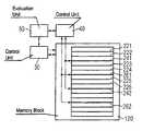
- FIG. 2A further exemplary embodiment of an integrated memory is illustrated in FIG. 2 , where there is also a logical assignment of the row lines of the memory block 120 to the regular memory area and the first and second test cell areas.
- the row lines which are logically associated with the different areasare not physically arranged in a blockwise manner, but rather are intermixed.
- the row lines 221 - 226are part of the regular memory area
- the row lines 241 , 242are part of the first test cell area
- the row lines 261 , 262are part of the second test cell area.
- FIG. 2shows only a small number of row lines, for the sake of clarity. In practice, the number is significantly larger; by way of example, a 128 Mbit DRAM chip may include 4096 regular row lines and in each case 48 row lines in the two test cell areas.
- the arrangement scheme illustrated in FIG. 2can also be maintained, in principle, with the higher number of rows.
- test row lineshave the same average temperature as the regular row lines. Consequently, the retention behavior of the test cells represents a true reflection of the behavior of the regular memory cells.
- control unit 40 and the control unit 30keep a record of the addresses of the test rows 241 , 242 , 261 , 262 in the memory block 120 in order to avoid incorrect accesses.
- a register 32 , 42 , 44 of sufficiently high resolutionis in each case used for the two test cell arrays and the regular memory cell array.
- the binary value of the register in each casespecifies the refresh time of the relevant cell area in milliseconds.
- the register of the regular memory area 32contains, after system initialization, the binary value “0000001000000”, for 64 ms
- the register 42 of the first test cell areacontains the binary value “0000010000000” for 128 ms
- the register 44 of the second test cell areacontains the binary value “0000100000000” for 256 ms.
- all the registers 32 , 42 , 44are shifted by one bit toward the left or right, which corresponds to a doubling or a halving of the associated refresh time.
- a checkis made to determine whether the maximum values have been reached, that is to say, in the case of lengthening, whether the refresh time T ref is already 1024 ms, and in the case of a reduction, whether it is already 1 ms. The refresh times remain unchanged in both cases.
- the memory devicecan thus react to altered external influences by adapting the refresh time.
- the memory deviceis thereby independent of operating and aging conditions.
- the connected controllerhas the possibility, in the so-called auto-refresh operating mode, of accessing the individual refresh timer values and of adapting its refresh rate to the worst (that is to say shortest) refresh time.
- the controllercan send a request signal to the memory devices within the module which drive the individual values of T ref from each of the devices of the module.
- the shortest refresh timecan then be determined, which is subsequently used for the refresh of each of the memory devices within the module.
- the refresh times T 1 and T 2are either determined once individually in the sense of a measurement request, or are determined permanently independently of the refresh time T ref and are stored in respective control registers.
- T 1 and T 2must be determined permanently, and each device of a group of devices or a memory module is able to follow its own refresh time T ref,i .
Landscapes
- Engineering & Computer Science (AREA)
- Microelectronics & Electronic Packaging (AREA)
- Dram (AREA)
- For Increasing The Reliability Of Semiconductor Memories (AREA)
Abstract
Description
- the retention time was set correctly by fuses/trimmer;
- the retention is identical for volatile logic ones (“1”) and logic zeros (“0”);
- the defective cells have been eliminated by redundancy activation;
- the inherent chip heating does not increase in operation throughout the lifetime of the product;
- the retention susceptibility does not increase or vary with respect to time, as in the case of the so-called “variable retention time”;
- the actually tested temperature at which the retention time was determined is known precisely.
- the first refresh time Trefis lengthened, or is left unchanged after reaching a maximum refresh time Tmaxif no memory cell defects are detected in the first and second test areas;
- the first refresh time Trefis shortened, or is left unchanged after reaching a minimum refresh time Tminif memory cell defects are detected in both the first and the second test areas; and
- otherwise the first refresh time Trefis left unchanged.
- for each of the integrated memory devices, in response to a request signal from an external controller, the refresh time Trefthereof is determined and communicated to the controller;
- the controller determines the shortest of the refresh times; and
- the shortest refresh time that has been determined is subsequently used for refreshing each of the plurality of memory devices.
| TABLE 1 | ||||
| Result 1 (T1) | Result 2 (T2) | Measure | ||
| PASS | FAIL | Normal case: no change | ||
| PASS | PASS | if Tref< Tmax: | ||
| double Tref, T1, T2 | ||||
| FAIL | FAIL | if Tref> Tmin: | ||
| halve Tref, T1, T2 | ||||
| FAIL | PASS | should not occur: | ||
| no change | ||||
Claims (20)
Priority Applications (1)
| Application Number | Priority Date | Filing Date | Title |
|---|---|---|---|
| US10/699,231US6940774B2 (en) | 2001-07-26 | 2003-10-31 | Integrated dynamic memory and operating method |
Applications Claiming Priority (4)
| Application Number | Priority Date | Filing Date | Title |
|---|---|---|---|
| DE10136544ADE10136544B4 (en) | 2001-07-26 | 2001-07-26 | Integrated dynamic memory and operating procedures |
| DE10136544.6 | 2001-07-26 | ||
| US10/206,299US6731552B2 (en) | 2001-07-26 | 2002-07-26 | Integrated dynamic memory and operating method |
| US10/699,231US6940774B2 (en) | 2001-07-26 | 2003-10-31 | Integrated dynamic memory and operating method |
Related Parent Applications (1)
| Application Number | Title | Priority Date | Filing Date |
|---|---|---|---|
| US10/206,299Continuation-In-PartUS6731552B2 (en) | 2001-07-26 | 2002-07-26 | Integrated dynamic memory and operating method |
Publications (2)
| Publication Number | Publication Date |
|---|---|
| US20040090853A1 US20040090853A1 (en) | 2004-05-13 |
| US6940774B2true US6940774B2 (en) | 2005-09-06 |
Family
ID=32231827
Family Applications (1)
| Application Number | Title | Priority Date | Filing Date |
|---|---|---|---|
| US10/699,231Expired - Fee RelatedUS6940774B2 (en) | 2001-07-26 | 2003-10-31 | Integrated dynamic memory and operating method |
Country Status (1)
| Country | Link |
|---|---|
| US (1) | US6940774B2 (en) |
Cited By (10)
| Publication number | Priority date | Publication date | Assignee | Title |
|---|---|---|---|---|
| US20090003099A1 (en)* | 2007-06-28 | 2009-01-01 | Safvi Anwar | Memory test mode for charge retention testing |
| US20100054070A1 (en)* | 2004-07-15 | 2010-03-04 | Micron Technology, Inc. | Method and system for controlling refresh to avoid memory cell data losses |
| US20100122019A1 (en)* | 2008-11-10 | 2010-05-13 | David Flynn | Apparatus, system, and method for managing physical regions in a solid-state storage device |
| US7836374B2 (en) | 2004-05-06 | 2010-11-16 | Micron Technology, Inc. | Memory controller method and system compensating for memory cell data losses |
| US7894289B2 (en)* | 2006-10-11 | 2011-02-22 | Micron Technology, Inc. | Memory system and method using partial ECC to achieve low power refresh and fast access to data |
| US7900120B2 (en) | 2006-10-18 | 2011-03-01 | Micron Technology, Inc. | Memory system and method using ECC with flag bit to identify modified data |
| US20140019812A1 (en)* | 2012-07-16 | 2014-01-16 | HGST Netherlands B.V. | System and method for maintaining data integrity on a storage medium |
| US20150043292A1 (en)* | 2013-08-09 | 2015-02-12 | SK Hynix Inc. | Memory, memory system including the same and method for operating memory |
| TWI613664B (en)* | 2013-06-28 | 2018-02-01 | 愛思開海力士有限公司 | Memory and memory system including the same |
| US12073908B2 (en) | 2021-03-12 | 2024-08-27 | Micron Technology, Inc. | On-die heater devices for memory devices and memory modules |
Families Citing this family (5)
| Publication number | Priority date | Publication date | Assignee | Title |
|---|---|---|---|---|
| KR100691489B1 (en)* | 2005-03-31 | 2007-03-09 | 주식회사 하이닉스반도체 | Self-Refresh Cycle Selection Circuit and Method for Testing Semiconductor Memory Devices |
| US20080056051A1 (en)* | 2006-08-31 | 2008-03-06 | Peter Mayer | Memory with memory banks and mode registers and method of operating a memory |
| US9324433B2 (en)* | 2011-04-25 | 2016-04-26 | Microsoft Technology Licensing, Llc | Intelligent flash reprogramming |
| US10109339B1 (en) | 2017-07-28 | 2018-10-23 | Micron Technology, Inc. | Memory devices with selective page-based refresh |
| US11055226B2 (en)* | 2018-06-29 | 2021-07-06 | Intel Corporation | Mitigation of cache-latency based side-channel attacks |
Citations (6)
| Publication number | Priority date | Publication date | Assignee | Title |
|---|---|---|---|---|
| US5808952A (en) | 1996-10-28 | 1998-09-15 | Silicon Magic Corporation | Adaptive auto refresh |
| US5943280A (en)* | 1997-07-16 | 1999-08-24 | Mitsubishi Denki Kabushiki Kaisha | Semiconductor memory device which can be tested while selecting word lines successively at high speed |
| US6141280A (en) | 1997-12-30 | 2000-10-31 | Hyundai Electronics Industries Co., Ltd. | Refresh period automatic detecting device for semiconductor memory device, method of automatically detecting refresh period, and refresh period output device |
| US6381188B1 (en) | 1999-01-12 | 2002-04-30 | Samsung Electronics Co., Ltd. | DRAM capable of selectively performing self-refresh operation for memory bank |
| US6529433B2 (en) | 2001-04-03 | 2003-03-04 | Hynix Semiconductor, Inc. | Refresh mechanism in dynamic memories |
| US6570802B2 (en) | 2000-11-15 | 2003-05-27 | Matsushita Electric Industrial Co., Ltd. | Semiconductor memory device |
- 2003
- 2003-10-31USUS10/699,231patent/US6940774B2/ennot_activeExpired - Fee Related
Patent Citations (6)
| Publication number | Priority date | Publication date | Assignee | Title |
|---|---|---|---|---|
| US5808952A (en) | 1996-10-28 | 1998-09-15 | Silicon Magic Corporation | Adaptive auto refresh |
| US5943280A (en)* | 1997-07-16 | 1999-08-24 | Mitsubishi Denki Kabushiki Kaisha | Semiconductor memory device which can be tested while selecting word lines successively at high speed |
| US6141280A (en) | 1997-12-30 | 2000-10-31 | Hyundai Electronics Industries Co., Ltd. | Refresh period automatic detecting device for semiconductor memory device, method of automatically detecting refresh period, and refresh period output device |
| US6381188B1 (en) | 1999-01-12 | 2002-04-30 | Samsung Electronics Co., Ltd. | DRAM capable of selectively performing self-refresh operation for memory bank |
| US6570802B2 (en) | 2000-11-15 | 2003-05-27 | Matsushita Electric Industrial Co., Ltd. | Semiconductor memory device |
| US6529433B2 (en) | 2001-04-03 | 2003-03-04 | Hynix Semiconductor, Inc. | Refresh mechanism in dynamic memories |
Cited By (35)
| Publication number | Priority date | Publication date | Assignee | Title |
|---|---|---|---|---|
| US7836374B2 (en) | 2004-05-06 | 2010-11-16 | Micron Technology, Inc. | Memory controller method and system compensating for memory cell data losses |
| US9064600B2 (en) | 2004-05-06 | 2015-06-23 | Micron Technology, Inc. | Memory controller method and system compensating for memory cell data losses |
| US8689077B2 (en) | 2004-05-06 | 2014-04-01 | Micron Technology, Inc. | Memory controller method and system compensating for memory cell data losses |
| US20110060961A1 (en)* | 2004-05-06 | 2011-03-10 | Micro Technology, Inc. | Memory controller method and system compensating for memory cell data losses |
| US8446783B2 (en) | 2004-07-15 | 2013-05-21 | Micron Technology, Inc. | Digit line comparison circuits |
| US7898892B2 (en) | 2004-07-15 | 2011-03-01 | Micron Technology, Inc. | Method and system for controlling refresh to avoid memory cell data losses |
| US20110134708A1 (en)* | 2004-07-15 | 2011-06-09 | Micron Technology, Inc. | Method and system for controlling refresh to avoid memory cell data losses |
| US20100054070A1 (en)* | 2004-07-15 | 2010-03-04 | Micron Technology, Inc. | Method and system for controlling refresh to avoid memory cell data losses |
| US8279683B2 (en) | 2004-07-15 | 2012-10-02 | Micron Technology, Inc. | Digit line comparison circuits |
| US20130139029A1 (en)* | 2006-10-11 | 2013-05-30 | Micron Technology, Inc. | Memory system and method using partial ecc to achieve low power refresh and fast access to data |
| US9286161B2 (en)* | 2006-10-11 | 2016-03-15 | Micron Technology, Inc. | Memory system and method using partial ECC to achieve low power refresh and fast access to data |
| US20140359391A1 (en)* | 2006-10-11 | 2014-12-04 | Micron Technology, Inc. | Memory system and method using partial ecc to achieve low power refresh and fast access to data |
| US8832522B2 (en)* | 2006-10-11 | 2014-09-09 | Micron Technology, Inc. | Memory system and method using partial ECC to achieve low power refresh and fast access to data |
| US20110138251A1 (en)* | 2006-10-11 | 2011-06-09 | Pawlowski J Thomas | Memory system and method using partial ecc to achieve low power refresh and fast access to data |
| US8359517B2 (en)* | 2006-10-11 | 2013-01-22 | Micron Technology, Inc. | Memory system and method using partial ECC to achieve low power refresh and fast access to data |
| US7894289B2 (en)* | 2006-10-11 | 2011-02-22 | Micron Technology, Inc. | Memory system and method using partial ECC to achieve low power refresh and fast access to data |
| US20110138252A1 (en)* | 2006-10-18 | 2011-06-09 | Pawlowski J Thomas | Memory system and method using ecc with flag bit to identify modified data |
| US8601341B2 (en) | 2006-10-18 | 2013-12-03 | Micron Technologies, Inc. | Memory system and method using ECC with flag bit to identify modified data |
| US8413007B2 (en) | 2006-10-18 | 2013-04-02 | Micron Technology, Inc. | Memory system and method using ECC with flag bit to identify modified data |
| US8880974B2 (en) | 2006-10-18 | 2014-11-04 | Micron Technology, Inc. | Memory system and method using ECC with flag bit to identify modified data |
| US7900120B2 (en) | 2006-10-18 | 2011-03-01 | Micron Technology, Inc. | Memory system and method using ECC with flag bit to identify modified data |
| US20090003099A1 (en)* | 2007-06-28 | 2009-01-01 | Safvi Anwar | Memory test mode for charge retention testing |
| US7545698B2 (en)* | 2007-06-28 | 2009-06-09 | Intel Corporation | Memory test mode for charge retention testing |
| US8275933B2 (en) | 2008-11-10 | 2012-09-25 | Fusion-10, Inc | Apparatus, system, and method for managing physical regions in a solid-state storage device |
| US8725938B2 (en) | 2008-11-10 | 2014-05-13 | Fusion-Io, Inc. | Apparatus, system, and method for testing physical regions in a solid-state storage device |
| US20100122019A1 (en)* | 2008-11-10 | 2010-05-13 | David Flynn | Apparatus, system, and method for managing physical regions in a solid-state storage device |
| US20140019812A1 (en)* | 2012-07-16 | 2014-01-16 | HGST Netherlands B.V. | System and method for maintaining data integrity on a storage medium |
| US9055711B2 (en)* | 2012-07-16 | 2015-06-09 | HGST Netherlands B.V. | System and method for maintaining data integrity on a storage medium |
| TWI613664B (en)* | 2013-06-28 | 2018-02-01 | 愛思開海力士有限公司 | Memory and memory system including the same |
| KR20150018164A (en)* | 2013-08-09 | 2015-02-23 | 에스케이하이닉스 주식회사 | Memory, memory including the same and method for operating memory |
| US9123447B2 (en)* | 2013-08-09 | 2015-09-01 | SK Hynix Inc. | Memory, memory system including the same and method for operating memory |
| US20150043292A1 (en)* | 2013-08-09 | 2015-02-12 | SK Hynix Inc. | Memory, memory system including the same and method for operating memory |
| TWI611295B (en)* | 2013-08-09 | 2018-01-11 | 愛思開海力士有限公司 | Memory, memory system including the same and method for operating memory |
| KR102194791B1 (en) | 2013-08-09 | 2020-12-28 | 에스케이하이닉스 주식회사 | Memory, memory including the same and method for operating memory |
| US12073908B2 (en) | 2021-03-12 | 2024-08-27 | Micron Technology, Inc. | On-die heater devices for memory devices and memory modules |
Also Published As
| Publication number | Publication date |
|---|---|
| US20040090853A1 (en) | 2004-05-13 |
Similar Documents
| Publication | Publication Date | Title |
|---|---|---|
| US6731552B2 (en) | Integrated dynamic memory and operating method | |
| US11600314B2 (en) | Apparatuses and methods for sketch circuits for refresh binning | |
| US7836374B2 (en) | Memory controller method and system compensating for memory cell data losses | |
| US5933377A (en) | Semiconductor memory device and defect repair method for semiconductor memory device | |
| US6108252A (en) | Integrated circuit memory devices having self-test circuits therein and method of testing same | |
| US6965537B1 (en) | Memory system and method using ECC to achieve low power refresh | |
| US6940774B2 (en) | Integrated dynamic memory and operating method | |
| US8279683B2 (en) | Digit line comparison circuits | |
| US7975170B2 (en) | Memory refresh system and method | |
| US8509021B2 (en) | Methods, circuits, and systems to select memory regions | |
| US7526713B2 (en) | Low power cost-effective ECC memory system and method | |
| EP1255197B1 (en) | System and method for correcting soft errors in random access memory devices | |
| US6940773B2 (en) | Method and system for manufacturing DRAMs with reduced self-refresh current requirements | |
| US6728156B2 (en) | Memory array system | |
| US5432744A (en) | Dynamic semiconductor memory circuit | |
| EP0019150B1 (en) | Method of testing the operation of an internal refresh counter in a random access memory and circuit for the testing thereof | |
| KR910001534B1 (en) | Semiconductor memory device | |
| KR100212136B1 (en) | Test circuit of a dynamic memory device | |
| JPH07176702A (en) | Dynamic random access memory and its testing method |
Legal Events
| Date | Code | Title | Description |
|---|---|---|---|
| FEPP | Fee payment procedure | Free format text:PAYER NUMBER DE-ASSIGNED (ORIGINAL EVENT CODE: RMPN); ENTITY STATUS OF PATENT OWNER: LARGE ENTITY Free format text:PAYOR NUMBER ASSIGNED (ORIGINAL EVENT CODE: ASPN); ENTITY STATUS OF PATENT OWNER: LARGE ENTITY | |
| AS | Assignment | Owner name:INFINEON TECHNOLOGIES AG, GERMANY Free format text:ASSIGNMENT OF ASSIGNORS INTEREST;ASSIGNOR:PERNER, MARTIN;REEL/FRAME:016817/0341 Effective date:20031204 | |
| REMI | Maintenance fee reminder mailed | ||
| FPAY | Fee payment | Year of fee payment:4 | |
| SULP | Surcharge for late payment | ||
| AS | Assignment | Owner name:QIMONDA AG,GERMANY Free format text:ASSIGNMENT OF ASSIGNORS INTEREST;ASSIGNOR:INFINEON TECHNOLOGIES AG;REEL/FRAME:023768/0001 Effective date:20060425 Owner name:QIMONDA AG, GERMANY Free format text:ASSIGNMENT OF ASSIGNORS INTEREST;ASSIGNOR:INFINEON TECHNOLOGIES AG;REEL/FRAME:023768/0001 Effective date:20060425 | |
| FPAY | Fee payment | Year of fee payment:8 | |
| AS | Assignment | Owner name:INFINEON TECHNOLOGIES AG, GERMANY Free format text:ASSIGNMENT OF ASSIGNORS INTEREST;ASSIGNOR:QIMONDA AG;REEL/FRAME:035623/0001 Effective date:20141009 | |
| AS | Assignment | Owner name:POLARIS INNOVATIONS LIMITED, IRELAND Free format text:ASSIGNMENT OF ASSIGNORS INTEREST;ASSIGNOR:INFINEON TECHNOLOGIES AG;REEL/FRAME:036723/0021 Effective date:20150708 | |
| REMI | Maintenance fee reminder mailed | ||
| LAPS | Lapse for failure to pay maintenance fees | Free format text:PATENT EXPIRED FOR FAILURE TO PAY MAINTENANCE FEES (ORIGINAL EVENT CODE: EXP.) | |
| STCH | Information on status: patent discontinuation | Free format text:PATENT EXPIRED DUE TO NONPAYMENT OF MAINTENANCE FEES UNDER 37 CFR 1.362 | |
| FP | Lapsed due to failure to pay maintenance fee | Effective date:20170906 |