US6939767B2 - Multi-bit non-volatile integrated circuit memory and method therefor - Google Patents
Multi-bit non-volatile integrated circuit memory and method thereforDownload PDFInfo
- Publication number
- US6939767B2 US6939767B2US10/716,956US71695603AUS6939767B2US 6939767 B2US6939767 B2US 6939767B2US 71695603 AUS71695603 AUS 71695603AUS 6939767 B2US6939767 B2US 6939767B2
- Authority
- US
- United States
- Prior art keywords
- charge storage
- control gates
- forming
- layer
- control gate
- Prior art date
- Legal status (The legal status is an assumption and is not a legal conclusion. Google has not performed a legal analysis and makes no representation as to the accuracy of the status listed.)
- Expired - Fee Related
Links
Images


Classifications
- H—ELECTRICITY
- H10—SEMICONDUCTOR DEVICES; ELECTRIC SOLID-STATE DEVICES NOT OTHERWISE PROVIDED FOR
- H10B—ELECTRONIC MEMORY DEVICES
- H10B41/00—Electrically erasable-and-programmable ROM [EEPROM] devices comprising floating gates
- H10B41/30—Electrically erasable-and-programmable ROM [EEPROM] devices comprising floating gates characterised by the memory core region
- B—PERFORMING OPERATIONS; TRANSPORTING
- B82—NANOTECHNOLOGY
- B82Y—SPECIFIC USES OR APPLICATIONS OF NANOSTRUCTURES; MEASUREMENT OR ANALYSIS OF NANOSTRUCTURES; MANUFACTURE OR TREATMENT OF NANOSTRUCTURES
- B82Y10/00—Nanotechnology for information processing, storage or transmission, e.g. quantum computing or single electron logic
- H—ELECTRICITY
- H10—SEMICONDUCTOR DEVICES; ELECTRIC SOLID-STATE DEVICES NOT OTHERWISE PROVIDED FOR
- H10B—ELECTRONIC MEMORY DEVICES
- H10B69/00—Erasable-and-programmable ROM [EPROM] devices not provided for in groups H10B41/00 - H10B63/00, e.g. ultraviolet erasable-and-programmable ROM [UVEPROM] devices
- H—ELECTRICITY
- H10—SEMICONDUCTOR DEVICES; ELECTRIC SOLID-STATE DEVICES NOT OTHERWISE PROVIDED FOR
- H10D—INORGANIC ELECTRIC SEMICONDUCTOR DEVICES
- H10D30/00—Field-effect transistors [FET]
- H10D30/60—Insulated-gate field-effect transistors [IGFET]
- H10D30/68—Floating-gate IGFETs
- H10D30/687—Floating-gate IGFETs having more than two programming levels
- H—ELECTRICITY
- H10—SEMICONDUCTOR DEVICES; ELECTRIC SOLID-STATE DEVICES NOT OTHERWISE PROVIDED FOR
- H10D—INORGANIC ELECTRIC SEMICONDUCTOR DEVICES
- H10D30/00—Field-effect transistors [FET]
- H10D30/60—Insulated-gate field-effect transistors [IGFET]
- H10D30/68—Floating-gate IGFETs
- H10D30/6891—Floating-gate IGFETs characterised by the shapes, relative sizes or dispositions of the floating gate electrode
- H10D30/6893—Floating-gate IGFETs characterised by the shapes, relative sizes or dispositions of the floating gate electrode wherein the floating gate has multiple non-connected parts, e.g. multi-particle floating gate
Definitions
- This inventionrelates generally to integrated circuits, and more particularly to a multi-bit non-volatile memory and method therefor.
- Some multi-bit non-volatile memory cellsstore more than one bit per cell by including more than one separate charge storage regions.
- the minimum area required by a memory cellis determined, at least in part, by the minimum pitch of the word lines.
- more than fifty percent of the surface area of a memory cellis not used for storing information, that is, the extra surface area may be referred to as “dead space”.
- FIGS. 1–4illustrate, in a cross-sectional view, a method for forming a non-volatile memory cell in accordance with one embodiment of the present invention.
- FIG. 5illustrates, in a top-down view, a layout of a semiconductor device including the non-volatile memory cell of FIG. 4 .
- FIG. 6illustrates a cross-section of the non-volatile memory cell of FIG. 5 along a line 6 — 6 .
- FIG. 7illustrates, in a top-down view, a layout of a semiconductor device including a non-volatile memory cell in accordance with another embodiment of the present invention.
- FIG. 8illustrates a cross-section of the semiconductor device of FIG. 7 along a line 8 — 8 .
- FIG. 9illustrates a cross-section of the of the semiconductor device of FIG. 7 along a line 9 — 9 .
- FIG. 10illustrates, in block diagram form, an integrated circuit including a non-volatile memory in accordance with the present invention.
- FIG. 11illustrates, in schematic diagram form, a non-volatile memory in accordance with the present invention.
- the present inventionprovides a high density virtual ground NOR type multi-bit flash EEPROM (electrically erasable programmable read only memory) non-volatile memory.
- the non-volatile memoryincludes at least two buried bit lines formed within the semiconductor substrate, a charge storage layer overlying the semiconductor substrate; a first control gate overlying the charge storage layer; an insulating liner overlying the first control gate; and first and second sidewall spacer control gates. Multiple programmable charge storage regions are created within the charge storage layer beneath respective ones of the control gates.
- a very dense multi-bit non-volatile memorycan be manufactured. For example, in one embodiment, six bits of information can be stored in the amount of space required to store just two bits in a prior art non-volatile memory.
- FIGS. 1–4illustrate, in a cross-sectional view, a method for forming a non-volatile memory cell in accordance with one embodiment of the present invention.
- FIG. 1illustrates a semiconductor device 10 having a substrate 12 and a charge storage stack 14 formed thereon.
- Substrate 12is formed from a semiconductive material having a P+ conductivity type.
- Charge storage stack 14includes insulating layers 16 and 20 and a nitride layer 18 .
- Insulating layer 16is formed in substrate 12 having a thickness of between about 15 to 60 angstroms.
- Charge storage layer 18is deposited on the surface of insulating layer 16 having a thickness of between about 50 to 150 angstroms.
- Insulating layer 20is formed on charge storage layer 18 having a thickness of between about 40 to 100 angstroms.
- insulating layer 16is formed from an oxide grown on the surface of substrate 12
- charge storage layer 18is deposited nitride
- insulating layer 20is an oxide deposited on charge storage layer 18 .
- charge storage layer 18may be an Si 3 N 4 layer, an oxynitride layer, a layer consisting of a plurality of nanocrystals, a layer consisting of a plurality of nanoclusters, and any combinations thereof.
- charge storage layer 18consists of a material that is not electrically conductive, and thus provides for a localized storage of injected charge.
- charge storage stack 14may be an ONO stack, an oxide-nanocrystal-oxide stack, and an oxide-nanocluster-oxide stack.
- another insulating layer 22may be formed on top of insulating layer 20 having a thickness of about 50 angstroms. Insulating layer 22 is preferably formed from nitride and prevents a subsequent gate etch process step from inadvertently removing insulating layer 20 .
- a conductive layer 24is deposited on insulating 22 . In the illustrated embodiment, conductive layer 24 is formed from highly doped polysilicon having a thickness of about 2000 angstroms or less. The polysilicon doping concentration is usually between 10 19 and 10 21 dopant atoms per cubic centimeter. In other embodiments, conductive layer 24 may include a metal.
- FIG. 2illustrates a step of patterning conductive layer 24 to form a plurality of control gates represented by control gates 26 and 28 .
- a masking stepis used to form control gates 26 and 28 .
- Control gates 26 and 28have a width of about 0.13 microns in the illustrated embodiment, which is a minimum dimension for the intended manufacturing process. In addition, the control gates are about 0.13 microns apart. In other embodiments, the minimum dimension may be different. Note that control gates also form word lines for accessing the memory cells of the array.
- FIG. 3illustrates a step of forming an insulating layer 30 around control gates 26 and 28 .
- Insulating layer 30is formed by thermal oxidation of the sides and top of polysilicon control gates 26 and 28 , and forms an insulating liner to isolate the control gates 26 and 28 from sidewall spacers formed later in FIG. 4 .
- insulating layer 30is about 200 angstroms thick.
- insulating layer 30may be deposited oxide or another deposited insulating material.
- FIG. 4illustrates a step of forming conductive sidewall spacers 32 , 34 , 36 , and 38 on the sides of control gates 26 and 28 for semiconductor device 10 .
- Conductive sidewall spacers 32 , 34 , 36 , and 38are formed from highly doped polysilicon.
- Sidewall spacers 32 , 34 , 36 , and 38are formed from deposited polysilicon using a conventional sidewall spacer manufacturing process.
- the deposited polysiliconis doped with a concentration of dopant atoms that is similar to the doping concentration in the conducting layer 24 .
- the sidewall spacersform word lines for applying address signals to access memory cells, and function as control gates.
- the sidewall spacersmay be formed from a metal.
- FIG. 5illustrates, in a top-down view, a layout of semiconductor device 10 .
- the cross-sectional view of FIG. 4is along line 4 — 4 in FIG. 5 .
- Semiconductor device 10is a portion of a non-volatile memory.
- patterned polysilicon lines 26 and 28 , and sidewall spacers 32 , 34 , 36 , and 38form both control gates and word lines for a non-volatile memory in accordance with one embodiment of the present invention.
- Sidewall spacers 32 , 34 , 36 , and 38also form word lines.
- the sidewall spacersbeing isolated from control gates 26 and 28 by protective liner 30 .
- Active region 40is formed between bit lines 45 and 47 .
- Active region 42is formed between bit lines 47 and 49 .
- bit lines 45 , 47 , and 49are buried bit lines diffused into substrate 12 .
- chargeaccumulates in areas of nitride layer 18 at junctions of the word lines and bit lines.
- a bitcellmust be electrically selected for programming. Most of the charge accumulates at the edges of the active regions. In the illustrated embodiment, charge is stored under both edges of active regions under each of the word lines.
- two charge storage regions 41are located under word line 32
- two charge storage regions 43are located under word line 26
- two charge storage regions 44are located under word line 34
- two charge storage regions 46are located under word line 36
- two charge storage regions 51are located under word line 28
- two charge storage regions 58are located under word line 38 .
- charge storage regions in active region 42There are similar charge storage regions in active region 42 that are not shown.
- Each charge storage regioncan store one bit of information. Therefore, in the illustrated embodiment, up to six (6) charge storage regions are available in a unit cell (i.e. at the intersection of a single word line and active region).
- the memory of the present inventionrequires the same or less surface area to store a single bit than some prior art two-bit per cell non-volatile memories. Consequently, the area per bit required for the bitcell of the present invention is much smaller than the area per bit required in a prior art two-bit per cell non-volatile memory.
- FIG. 6illustrates a cross-sectional view of the semiconductor device 10 of FIG. 5 along a line 6 — 6 .
- bit lines 45 , 47 , and 49are formed by diffusing dopants that create N-type conductivity into the substrate 12 which is doped to have P-type conductivity. Note that in other embodiments the conductivity types may be reversed.
- a typical dopant concentration in the P-type substrateis between 10 17 and 10 18 atoms per cubic centimeter.
- a typical dopant concentration in the N+-type bitlinesis between 10 19 and 10 21 atoms per cubic centimeter.
- Charge storage stack 14is illustrated with charge storage layer 18 between insulating layers 16 and 20 .
- the optional insulating layer 22is formed over insulating layer 20 as described above.
- chargeis collected in charge storage regions of charge storage layer 18 such as one of the two charge storage regions 43 . As can be seen in FIG. 6 , the charge is collected at the edges of the active regions 40 and 42 below the control gates and above the bit lines.
- FIG. 7illustrates, in a top-down view, a layout of a semiconductor device 39 in accordance with another embodiment of the present invention.
- Semiconductor device 39differs from semiconductor device 10 of FIG. 5 in that instead of using conventional polysilicon sidewall spacers for the additional word lines, the word lines are formed by depositing polysilicon in the spaces between insulating layers 30 . The result is fewer charge storage regions and word lines having larger cross-sectional areas as is illustrated in the cross-sectional view of FIG. 8 .
- semiconductor device 39includes additional word lines 50 , 52 , and 54 formed in this manner. Additional word lines 50 , 52 , and 54 are separated from word lines 26 and 28 by oxide layers 30 .
- Chargeis stored at the edges, or periphery, of active regions 40 and 42 under each of the word lines.
- two charge storage regions 53are located under word line 50
- two charge storage regions 55are located under word line 26
- two charge storage regions 56are located under word line 52
- two charge storage regions 57are located under word line 28
- two charge storage regions 59are located under word line 54 .
- the semiconductor device 39 of FIG. 7provides a more dense memory than the prior art.
- FIG. 8illustrates a cross-section of semiconductor device 39 of FIG. 7 along a line 8 — 8 .
- the first stepsare the same as described above regarding FIG. 1 , FIG. 2 and FIG. 3 .
- the spaces between the word linesare filled with polysilicon to form control gates/word lines 50 , 52 , and 54 .
- Control gates 50 , 52 , and 54are formed by depositing a conformal layer of conductive material overlying control gates 26 and 28 followed by anisotropic etching of the conformal layer, or by a combination of multiple deposition and etch processes of various types.
- word lines 50 , 52 , and 54may be formed by merging the sidewall spacers illustrated in FIG. 4 until they contact each other, or grow together.
- FIG. 9illustrates a cross-section of the of semiconductor device 39 of FIG. 7 along a line 9 — 9 .
- the cross-sectional view of semiconductor device 39 along word line 26is similar to the cross-sectional view of semiconductor device 10 illustrated in FIG. 6 .
- bit lines 45 , 47 , and 49are formed by diffusing dopants that create N-type conductivity in the P doped substrate 12 .
- the conductivity typesmay be different or reversed.
- a typical dopant concentration in the P-type substrateis between 10 17 and 10 18 atoms per cubic centimeter.
- a typical dopant concentration in the N+-type bit linesis between 10 19 and 10 21 atoms per cubic centimeter.
- Charge storage stack 14is illustrated with charge storage layer 18 between insulating layers 16 and 20 .
- the optional insulating layer 22is formed over insulating layer 20 as described above.
- chargeis collected in selected charge storage regions of charge storage layer 18 such as charge storage regions 55 .
- chargeis collected at the edges of the active regions 40 and 42 below the control gates, such as for example, charge storage regions 55 under word line 26 .
- FIG. 10illustrates, in block diagram form, an integrated circuit 70 .
- Integrated circuit 70includes a central processing unit 74 bi-directionally coupled to a non-volatile memory array 72 .
- a detailed schematic diagram of non-volatile memory array 72is illustrated in FIG. 11 .
- integrated circuit 70may include additional circuitry (not shown), such as for example, co-processors, input/output (I/O) ports, additional memory, etc.
- Non-volatile memory 72includes a plurality of non-volatile memory cells in accordance with the present invention.
- an integrated circuit memory 76separate from integrated circuit 70 , may be bi-directionally coupled to integrated circuit 70 and include a plurality of memory cells in accordance with the present invention.
- Integrated circuit memory 76may comprise memory cells as described above for either embodiment of the present invention.
- Integrated circuit memory 76may comprise memory cells as described above for either embodiment of the present invention.
- Implementing memory cells of the present invention in integrated circuit 70provides the advantage of requiring less surface area of integrated circuit 70 than prior art multi-bit non-volatile memory cells. If the memory array requires less surface area, then the integrated circuit can be made smaller and less expensive to manufacture.
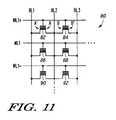
- FIG. 11illustrates, in schematic diagram form, non-volatile memory array portion 80 in accordance with the present invention.
- Non-volatile memory array portion 80corresponds to memory layout 39 of FIG. 7 .
- Memory array portion 80includes non-volatile memory cells 82 , 84 , 86 , 88 , 90 , and 92 .
- Each memory cell in FIG. 11schematically represents an intersection of a word line and two bit lines for storing two bits of information as illustrated in, for example, FIG. 7 .
- Two charge storage regionsare located at each intersection at the edges of the active region underlying the control gate.
- two charge storage regions of memory cell 82are labeled A and A′
- two charge storage regions of memory cell 84are labeled B and B′.
- a control gate of each of cells 86 and 88is coupled to a word line labeled WL 1 .
- Word line WL 1corresponds to, for example, word line 26 of FIG. 7 .
- a control gate of cells 82 and 84are coupled to a word line labeled WL 1 +, corresponding to one of word lines 50 or 52 of FIG. 7 .
- a control gate of cells 90 and 92are coupled to a word line labeled WL ⁇ , corresponding to the other one of word lines 50 or 52 of FIG. 7 .
- Each of the memory cellsis coupled to two bit lines.
- bits 82 , 86 , and 90are coupled to bit lines BL 1 and BL 2
- cells 84 , 88 , and 92are coupled to bit lines BL 2 and BL 3
- Bit line BL 1corresponds to, for example, bit line 45
- bit line BL 2corresponds to bit line 47
- bit line BL 3corresponds to bit line 49 .
- Each of the charge storage regionscan be programmed, read, and erased separately.
- Hot carrier injectionis the mechanism used to program each charge storage region and Fowler-Nordheim tunneling is the mechanism used to erase each charge storage region.
- other methodssuch as for example, Fowler-Nordheim tunneling, may be used for programming.
- the memory array of the present inventionis very dense as compared to the prior art, the bit lines are relatively more closely spaced. Because of the close spacing, capacitive coupling between the bit lines can cause inadvertent programming of cells that are adjacent to a cell being programmed. To prevent the effects of capacitive coupling, or cross-coupling, the adjacent bit lines are held at an intermediate voltage level.
- word line WL 1 +is provided with about 6 volts and bit line BL 2 is at 3 volts. Also, adjacent word line WL 1 is at zero volts, bit line BL 1 is held at zero volts, and bit line BL 3 is at an intermediate voltage of, for example, 1.5 volts to prevent the possibility of unintentionally programming charge storage region B in cell 84 .
- word line WL 1 +is provided with about 6 volts and bit line BL 2 is at 3 volts. Also, adjacent word line WL 1 is at zero volts, bit line BL 1 is at the intermediate voltage of 1.5 volts, and BL 3 is at zero volts.
- the substrate biasis held at less than or equal to zero volts.
- word line WL 1 +is provided with 3 volts and bit line BL 1 is provided with 1.5 volts.
- the logic state of region A of cell 82is sensed on bit line BL 1 .
- word line WL 1 and bit line BL 3are both held at zero volts and the substrate is biased at a voltage of less than or equal to zero volts.
- word line WL 1 +is provided with 3 volts and bit line BL 3 is provided with 1.5 volts.
- the logic state of region B of cell 84is sensed on bit line BL 3 .
- word line WL 1 , bit line BL 1are both held at zero volts and the substrate is biased at zero volts.
- the arrayis bulk erased by floating all of the bit lines and applying ⁇ 6 volts to the word lines while the substrate is biased at +6 volts.
- the bit linescan be biased at a voltage that is identical to the substrate during the erase process.
- Yet another methodis to only bias one or few selected word lines to, for example, ⁇ 6 volts and leave all other word lines at a bias of zero volts, and bias the substrate at +6 volts. In this case, only the cells connected to the biased word line or word lines will be erased.
- the substrateis kept at zero volts, the bit lines are biased to +6 volts, and the word lines are biased to ⁇ 6 volts.
- Yet another methodis to only bias one or a few selected word lines to, for example, ⁇ 6 volts, and bias all bit lines to +6 volts. In this case, only the cells connected to the biased word line or word lines will be erased.
Landscapes
- Engineering & Computer Science (AREA)
- Chemical & Material Sciences (AREA)
- Nanotechnology (AREA)
- Physics & Mathematics (AREA)
- Mathematical Physics (AREA)
- Theoretical Computer Science (AREA)
- Crystallography & Structural Chemistry (AREA)
- Semiconductor Memories (AREA)
- Non-Volatile Memory (AREA)
Abstract
Description
Claims (21)
Priority Applications (1)
| Application Number | Priority Date | Filing Date | Title |
|---|---|---|---|
| US10/716,956US6939767B2 (en) | 2003-11-19 | 2003-11-19 | Multi-bit non-volatile integrated circuit memory and method therefor |
Applications Claiming Priority (1)
| Application Number | Priority Date | Filing Date | Title |
|---|---|---|---|
| US10/716,956US6939767B2 (en) | 2003-11-19 | 2003-11-19 | Multi-bit non-volatile integrated circuit memory and method therefor |
Publications (2)
| Publication Number | Publication Date |
|---|---|
| US20050106812A1 US20050106812A1 (en) | 2005-05-19 |
| US6939767B2true US6939767B2 (en) | 2005-09-06 |
Family
ID=34574484
Family Applications (1)
| Application Number | Title | Priority Date | Filing Date |
|---|---|---|---|
| US10/716,956Expired - Fee RelatedUS6939767B2 (en) | 2003-11-19 | 2003-11-19 | Multi-bit non-volatile integrated circuit memory and method therefor |
Country Status (1)
| Country | Link |
|---|---|
| US (1) | US6939767B2 (en) |
Cited By (38)
| Publication number | Priority date | Publication date | Assignee | Title |
|---|---|---|---|---|
| US20050236662A1 (en)* | 2004-04-23 | 2005-10-27 | Lee Sang B | Flash memory device and method for fabricating the same, and programming and erasing method thereof |
| US20060216888A1 (en)* | 2005-03-23 | 2006-09-28 | Wei Zheng | High K stack for non-volatile memory |
| US20060267075A1 (en)* | 2005-05-26 | 2006-11-30 | Micron Technology, Inc. | Multi-state memory cell |
| US20070045720A1 (en)* | 2005-04-27 | 2007-03-01 | Hiroaki Kouketsu | Semiconductor device and manufacturing method therefor |
| US20070218669A1 (en)* | 2006-03-15 | 2007-09-20 | Li Chi Nan B | Method of forming a semiconductor device and structure thereof |
| WO2008112370A1 (en)* | 2007-03-13 | 2008-09-18 | Freescale Semiconductor Inc. | Electronic device including channel regions lying at different elevations and processes of forming the same |
| US20100314680A1 (en)* | 2008-10-31 | 2010-12-16 | Macronix International Co., Ltd. | Memory array |
| US7863128B1 (en) | 2005-02-04 | 2011-01-04 | Spansion Llc | Non-volatile memory device with improved erase speed |
| US8399310B2 (en) | 2010-10-29 | 2013-03-19 | Freescale Semiconductor, Inc. | Non-volatile memory and logic circuit process integration |
| US8658497B2 (en) | 2012-01-04 | 2014-02-25 | Freescale Semiconductor, Inc. | Non-volatile memory (NVM) and logic integration |
| US8669158B2 (en) | 2012-01-04 | 2014-03-11 | Mark D. Hall | Non-volatile memory (NVM) and logic integration |
| US8716089B1 (en) | 2013-03-08 | 2014-05-06 | Freescale Semiconductor, Inc. | Integrating formation of a replacement gate transistor and a non-volatile memory cell having thin film storage |
| US8716781B2 (en) | 2012-04-09 | 2014-05-06 | Freescale Semiconductor, Inc. | Logic transistor and non-volatile memory cell integration |
| US8728886B2 (en) | 2012-06-08 | 2014-05-20 | Freescale Semiconductor, Inc. | Integrating formation of a replacement gate transistor and a non-volatile memory cell using a high-k dielectric |
| US8741719B1 (en) | 2013-03-08 | 2014-06-03 | Freescale Semiconductor, Inc. | Integrating formation of a logic transistor and a non-volatile memory cell using a partial replacement gate technique |
| US8871598B1 (en) | 2013-07-31 | 2014-10-28 | Freescale Semiconductor, Inc. | Non-volatile memory (NVM) and high-k and metal gate integration using gate-first methodology |
| US8877585B1 (en) | 2013-08-16 | 2014-11-04 | Freescale Semiconductor, Inc. | Non-volatile memory (NVM) cell, high voltage transistor, and high-K and metal gate transistor integration |
| US8901632B1 (en) | 2013-09-30 | 2014-12-02 | Freescale Semiconductor, Inc. | Non-volatile memory (NVM) and high-K and metal gate integration using gate-last methodology |
| US8906764B2 (en) | 2012-01-04 | 2014-12-09 | Freescale Semiconductor, Inc. | Non-volatile memory (NVM) and logic integration |
| US8932925B1 (en) | 2013-08-22 | 2015-01-13 | Freescale Semiconductor, Inc. | Split-gate non-volatile memory (NVM) cell and device structure integration |
| US8951863B2 (en) | 2012-04-06 | 2015-02-10 | Freescale Semiconductor, Inc. | Non-volatile memory (NVM) and logic integration |
| US9006093B2 (en) | 2013-06-27 | 2015-04-14 | Freescale Semiconductor, Inc. | Non-volatile memory (NVM) and high voltage transistor integration |
| US9082650B2 (en) | 2013-08-21 | 2015-07-14 | Freescale Semiconductor, Inc. | Integrated split gate non-volatile memory cell and logic structure |
| US9082837B2 (en) | 2013-08-08 | 2015-07-14 | Freescale Semiconductor, Inc. | Nonvolatile memory bitcell with inlaid high k metal select gate |
| US9087913B2 (en) | 2012-04-09 | 2015-07-21 | Freescale Semiconductor, Inc. | Integration technique using thermal oxide select gate dielectric for select gate and apartial replacement gate for logic |
| US9111865B2 (en) | 2012-10-26 | 2015-08-18 | Freescale Semiconductor, Inc. | Method of making a logic transistor and a non-volatile memory (NVM) cell |
| US9112056B1 (en) | 2014-03-28 | 2015-08-18 | Freescale Semiconductor, Inc. | Method for forming a split-gate device |
| US9129855B2 (en) | 2013-09-30 | 2015-09-08 | Freescale Semiconductor, Inc. | Non-volatile memory (NVM) and high-k and metal gate integration using gate-first methodology |
| US9129996B2 (en) | 2013-07-31 | 2015-09-08 | Freescale Semiconductor, Inc. | Non-volatile memory (NVM) cell and high-K and metal gate transistor integration |
| US9136129B2 (en) | 2013-09-30 | 2015-09-15 | Freescale Semiconductor, Inc. | Non-volatile memory (NVM) and high-k and metal gate integration using gate-last methodology |
| US9231077B2 (en) | 2014-03-03 | 2016-01-05 | Freescale Semiconductor, Inc. | Method of making a logic transistor and non-volatile memory (NVM) cell |
| US9252152B2 (en) | 2014-03-28 | 2016-02-02 | Freescale Semiconductor, Inc. | Method for forming a split-gate device |
| US9252246B2 (en) | 2013-08-21 | 2016-02-02 | Freescale Semiconductor, Inc. | Integrated split gate non-volatile memory cell and logic device |
| US9257445B2 (en) | 2014-05-30 | 2016-02-09 | Freescale Semiconductor, Inc. | Method of making a split gate non-volatile memory (NVM) cell and a logic transistor |
| US9275864B2 (en) | 2013-08-22 | 2016-03-01 | Freescale Semiconductor,Inc. | Method to form a polysilicon nanocrystal thin film storage bitcell within a high k metal gate platform technology using a gate last process to form transistor gates |
| US9343314B2 (en) | 2014-05-30 | 2016-05-17 | Freescale Semiconductor, Inc. | Split gate nanocrystal memory integration |
| US9379222B2 (en) | 2014-05-30 | 2016-06-28 | Freescale Semiconductor, Inc. | Method of making a split gate non-volatile memory (NVM) cell |
| US9472418B2 (en) | 2014-03-28 | 2016-10-18 | Freescale Semiconductor, Inc. | Method for forming a split-gate device |
Citations (6)
| Publication number | Priority date | Publication date | Assignee | Title |
|---|---|---|---|---|
| US5023680A (en)* | 1988-11-10 | 1991-06-11 | Texas Instruments Incorporated | Floating-gate memory array with silicided buried bitlines and with single-step-defined floating gates |
| US5969383A (en) | 1997-06-16 | 1999-10-19 | Motorola, Inc. | Split-gate memory device and method for accessing the same |
| US6091102A (en)* | 1996-05-16 | 2000-07-18 | Altera Corporation | High-density nonvolatile memory cell |
| US6201282B1 (en) | 1998-05-05 | 2001-03-13 | Saifun Semiconductors Ltd. | Two bit ROM cell and process for producing same |
| US6630384B1 (en)* | 2001-10-05 | 2003-10-07 | Advanced Micro Devices, Inc. | Method of fabricating double densed core gates in sonos flash memory |
| US6635533B1 (en)* | 2003-03-27 | 2003-10-21 | Powerchip Semiconductor Corp. | Method of fabricating flash memory |
- 2003
- 2003-11-19USUS10/716,956patent/US6939767B2/ennot_activeExpired - Fee Related
Patent Citations (6)
| Publication number | Priority date | Publication date | Assignee | Title |
|---|---|---|---|---|
| US5023680A (en)* | 1988-11-10 | 1991-06-11 | Texas Instruments Incorporated | Floating-gate memory array with silicided buried bitlines and with single-step-defined floating gates |
| US6091102A (en)* | 1996-05-16 | 2000-07-18 | Altera Corporation | High-density nonvolatile memory cell |
| US5969383A (en) | 1997-06-16 | 1999-10-19 | Motorola, Inc. | Split-gate memory device and method for accessing the same |
| US6201282B1 (en) | 1998-05-05 | 2001-03-13 | Saifun Semiconductors Ltd. | Two bit ROM cell and process for producing same |
| US6630384B1 (en)* | 2001-10-05 | 2003-10-07 | Advanced Micro Devices, Inc. | Method of fabricating double densed core gates in sonos flash memory |
| US6635533B1 (en)* | 2003-03-27 | 2003-10-21 | Powerchip Semiconductor Corp. | Method of fabricating flash memory |
Non-Patent Citations (2)
| Title |
|---|
| Chang et al., "New SONOS Memory Using Source-Side Injection for Programming," IEEE Electron Device Letters, vol. 19, No. 7, Jul. 1998, pp. 253-255. |
| Eitan et al., "NROM: A Novel Localized Trapping, 2-Bit Nonvolatile Memory Cell," IEEE Electron Device Letters, vol. 21, No. 11, Nov. 2000, pp. 543-545. |
Cited By (56)
| Publication number | Priority date | Publication date | Assignee | Title |
|---|---|---|---|---|
| US20060146632A1 (en)* | 2004-04-23 | 2006-07-06 | Anam Semiconductor | Flash memory device and method for fabricating the same, and programming and erasing method thereof |
| US20050236662A1 (en)* | 2004-04-23 | 2005-10-27 | Lee Sang B | Flash memory device and method for fabricating the same, and programming and erasing method thereof |
| US7366026B2 (en)* | 2004-04-23 | 2008-04-29 | Dongbu Hitek Co., Ltd. | Flash memory device and method for fabricating the same, and programming and erasing method thereof |
| US7863128B1 (en) | 2005-02-04 | 2011-01-04 | Spansion Llc | Non-volatile memory device with improved erase speed |
| US7492001B2 (en)* | 2005-03-23 | 2009-02-17 | Spansion Llc | High K stack for non-volatile memory |
| US20060216888A1 (en)* | 2005-03-23 | 2006-09-28 | Wei Zheng | High K stack for non-volatile memory |
| US7855114B2 (en) | 2005-03-23 | 2010-12-21 | Spansion Llc | High K stack for non-volatile memory |
| US20090155992A1 (en)* | 2005-03-23 | 2009-06-18 | Spansion Llc | High k stack for non-volatile memory |
| US7626227B2 (en)* | 2005-04-27 | 2009-12-01 | Spansion Llc | Semiconductor device with reduced transistor breakdown voltage for preventing substrate junction currents |
| US20070045720A1 (en)* | 2005-04-27 | 2007-03-01 | Hiroaki Kouketsu | Semiconductor device and manufacturing method therefor |
| US7547599B2 (en) | 2005-05-26 | 2009-06-16 | Micron Technology, Inc. | Multi-state memory cell |
| US20090225602A1 (en)* | 2005-05-26 | 2009-09-10 | Micron Technology, Inc. | Multi-state memory cell |
| US20060267075A1 (en)* | 2005-05-26 | 2006-11-30 | Micron Technology, Inc. | Multi-state memory cell |
| US7521317B2 (en) | 2006-03-15 | 2009-04-21 | Freescale Semiconductor, Inc. | Method of forming a semiconductor device and structure thereof |
| WO2007130729A3 (en)* | 2006-03-15 | 2008-05-08 | Freescale Semiconductor Inc | Method of forming a semiconductor device and structure thereof |
| US20070218669A1 (en)* | 2006-03-15 | 2007-09-20 | Li Chi Nan B | Method of forming a semiconductor device and structure thereof |
| CN101405851B (en)* | 2006-03-15 | 2012-06-27 | 飞思卡尔半导体公司 | Method of forming a semiconductor device |
| US20080227254A1 (en)* | 2007-03-13 | 2008-09-18 | Freescale Semiconductor, Inc. | Electronic device including channel regions lying at different elevations and processes of forming the same |
| TWI424571B (en)* | 2007-03-13 | 2014-01-21 | Freescale Semiconductor Inc | Electronic device including channel regions at different heights and method of forming the same |
| US8803217B2 (en) | 2007-03-13 | 2014-08-12 | Freescale Semiconductor, Inc. | Process of forming an electronic device including a control gate electrode, a semiconductor layer, and a select gate electrode |
| WO2008112370A1 (en)* | 2007-03-13 | 2008-09-18 | Freescale Semiconductor Inc. | Electronic device including channel regions lying at different elevations and processes of forming the same |
| CN101647122B (en)* | 2007-03-13 | 2011-09-28 | 飞思卡尔半导体公司 | Electronic device including channel regions at different heights and process for forming the same |
| US20100314680A1 (en)* | 2008-10-31 | 2010-12-16 | Macronix International Co., Ltd. | Memory array |
| US8836005B2 (en)* | 2008-10-31 | 2014-09-16 | Macronix International Co., Ltd. | Memory array |
| US8399310B2 (en) | 2010-10-29 | 2013-03-19 | Freescale Semiconductor, Inc. | Non-volatile memory and logic circuit process integration |
| US8877568B2 (en) | 2010-10-29 | 2014-11-04 | Freescale Semiconductor, Inc. | Methods of making logic transistors and non-volatile memory cells |
| US8658497B2 (en) | 2012-01-04 | 2014-02-25 | Freescale Semiconductor, Inc. | Non-volatile memory (NVM) and logic integration |
| US8669158B2 (en) | 2012-01-04 | 2014-03-11 | Mark D. Hall | Non-volatile memory (NVM) and logic integration |
| US8906764B2 (en) | 2012-01-04 | 2014-12-09 | Freescale Semiconductor, Inc. | Non-volatile memory (NVM) and logic integration |
| US8951863B2 (en) | 2012-04-06 | 2015-02-10 | Freescale Semiconductor, Inc. | Non-volatile memory (NVM) and logic integration |
| US9087913B2 (en) | 2012-04-09 | 2015-07-21 | Freescale Semiconductor, Inc. | Integration technique using thermal oxide select gate dielectric for select gate and apartial replacement gate for logic |
| US8716781B2 (en) | 2012-04-09 | 2014-05-06 | Freescale Semiconductor, Inc. | Logic transistor and non-volatile memory cell integration |
| US8722493B2 (en) | 2012-04-09 | 2014-05-13 | Freescale Semiconductor, Inc. | Logic transistor and non-volatile memory cell integration |
| US8728886B2 (en) | 2012-06-08 | 2014-05-20 | Freescale Semiconductor, Inc. | Integrating formation of a replacement gate transistor and a non-volatile memory cell using a high-k dielectric |
| US9111865B2 (en) | 2012-10-26 | 2015-08-18 | Freescale Semiconductor, Inc. | Method of making a logic transistor and a non-volatile memory (NVM) cell |
| US8716089B1 (en) | 2013-03-08 | 2014-05-06 | Freescale Semiconductor, Inc. | Integrating formation of a replacement gate transistor and a non-volatile memory cell having thin film storage |
| US8741719B1 (en) | 2013-03-08 | 2014-06-03 | Freescale Semiconductor, Inc. | Integrating formation of a logic transistor and a non-volatile memory cell using a partial replacement gate technique |
| US9006093B2 (en) | 2013-06-27 | 2015-04-14 | Freescale Semiconductor, Inc. | Non-volatile memory (NVM) and high voltage transistor integration |
| US9129996B2 (en) | 2013-07-31 | 2015-09-08 | Freescale Semiconductor, Inc. | Non-volatile memory (NVM) cell and high-K and metal gate transistor integration |
| US8871598B1 (en) | 2013-07-31 | 2014-10-28 | Freescale Semiconductor, Inc. | Non-volatile memory (NVM) and high-k and metal gate integration using gate-first methodology |
| US9082837B2 (en) | 2013-08-08 | 2015-07-14 | Freescale Semiconductor, Inc. | Nonvolatile memory bitcell with inlaid high k metal select gate |
| US8877585B1 (en) | 2013-08-16 | 2014-11-04 | Freescale Semiconductor, Inc. | Non-volatile memory (NVM) cell, high voltage transistor, and high-K and metal gate transistor integration |
| US9252246B2 (en) | 2013-08-21 | 2016-02-02 | Freescale Semiconductor, Inc. | Integrated split gate non-volatile memory cell and logic device |
| US9082650B2 (en) | 2013-08-21 | 2015-07-14 | Freescale Semiconductor, Inc. | Integrated split gate non-volatile memory cell and logic structure |
| US8932925B1 (en) | 2013-08-22 | 2015-01-13 | Freescale Semiconductor, Inc. | Split-gate non-volatile memory (NVM) cell and device structure integration |
| US9275864B2 (en) | 2013-08-22 | 2016-03-01 | Freescale Semiconductor,Inc. | Method to form a polysilicon nanocrystal thin film storage bitcell within a high k metal gate platform technology using a gate last process to form transistor gates |
| US9129855B2 (en) | 2013-09-30 | 2015-09-08 | Freescale Semiconductor, Inc. | Non-volatile memory (NVM) and high-k and metal gate integration using gate-first methodology |
| US8901632B1 (en) | 2013-09-30 | 2014-12-02 | Freescale Semiconductor, Inc. | Non-volatile memory (NVM) and high-K and metal gate integration using gate-last methodology |
| US9136129B2 (en) | 2013-09-30 | 2015-09-15 | Freescale Semiconductor, Inc. | Non-volatile memory (NVM) and high-k and metal gate integration using gate-last methodology |
| US9231077B2 (en) | 2014-03-03 | 2016-01-05 | Freescale Semiconductor, Inc. | Method of making a logic transistor and non-volatile memory (NVM) cell |
| US9112056B1 (en) | 2014-03-28 | 2015-08-18 | Freescale Semiconductor, Inc. | Method for forming a split-gate device |
| US9252152B2 (en) | 2014-03-28 | 2016-02-02 | Freescale Semiconductor, Inc. | Method for forming a split-gate device |
| US9472418B2 (en) | 2014-03-28 | 2016-10-18 | Freescale Semiconductor, Inc. | Method for forming a split-gate device |
| US9257445B2 (en) | 2014-05-30 | 2016-02-09 | Freescale Semiconductor, Inc. | Method of making a split gate non-volatile memory (NVM) cell and a logic transistor |
| US9343314B2 (en) | 2014-05-30 | 2016-05-17 | Freescale Semiconductor, Inc. | Split gate nanocrystal memory integration |
| US9379222B2 (en) | 2014-05-30 | 2016-06-28 | Freescale Semiconductor, Inc. | Method of making a split gate non-volatile memory (NVM) cell |
Also Published As
| Publication number | Publication date |
|---|---|
| US20050106812A1 (en) | 2005-05-19 |
Similar Documents
| Publication | Publication Date | Title |
|---|---|---|
| US6939767B2 (en) | Multi-bit non-volatile integrated circuit memory and method therefor | |
| KR100221940B1 (en) | Semiconductor memory device | |
| US6580120B2 (en) | Two bit non-volatile electrically erasable and programmable memory structure, a process for producing said memory structure and methods for programming, reading and erasing said memory structure | |
| US7075146B2 (en) | 4F2 EEPROM NROM memory arrays with vertical devices | |
| US5999444A (en) | Nonvolatile semiconductor memory device and writing and erasing method of the same | |
| US7339239B2 (en) | Vertical NROM NAND flash memory array | |
| US5467308A (en) | Cross-point eeprom memory array | |
| US5705415A (en) | Process for forming an electrically programmable read-only memory cell | |
| US7369436B2 (en) | Vertical NAND flash memory device | |
| US6434053B1 (en) | Nonvolatile semiconductor memory device and method of operation thereof | |
| US6212103B1 (en) | Method for operating flash memory | |
| US8143667B2 (en) | Semiconductor device having non-volatile memory and method of fabricating the same | |
| KR100257661B1 (en) | Non-volatile memory cell structure and process for forming same | |
| US7723774B2 (en) | Non-diffusion junction split-gate nonvolatile memory cells and arrays, methods of programming, erasing, and reading thereof, and methods of manufacture | |
| JP4330670B2 (en) | Nonvolatile semiconductor memory device | |
| US7547941B2 (en) | NAND non-volatile two-bit memory and fabrication method | |
| US7355241B2 (en) | Non-volatile memory | |
| US7006378B1 (en) | Array architecture and operation methods for a nonvolatile memory | |
| US7391071B2 (en) | Nonvolatile memory devices with trenched side-wall transistors and method of fabricating the same | |
| US5804854A (en) | Memory cell array | |
| CN101345262A (en) | Semiconductor structure and method for reducing second bit effect of memory element | |
| TWI399834B (en) | Reverse flash memory with nitride charging storage gate and manufacturing method thereof | |
| US6329688B1 (en) | Nonvolatile semiconductor memory device and method of manufacturing the same |
Legal Events
| Date | Code | Title | Description |
|---|---|---|---|
| AS | Assignment | Owner name:MOTOROLA, INC., ILLINOIS Free format text:ASSIGNMENT OF ASSIGNORS INTEREST;ASSIGNORS:HOEFLER, ALEXANDER B.;CHANG, KO-MIN;REEL/FRAME:014726/0729 Effective date:20031119 | |
| AS | Assignment | Owner name:FREESCALE SEMICONDUCTOR, INC., TEXAS Free format text:ASSIGNMENT OF ASSIGNORS INTEREST;ASSIGNOR:MOTOROLA, INC;REEL/FRAME:015360/0718 Effective date:20040404 Owner name:FREESCALE SEMICONDUCTOR, INC.,TEXAS Free format text:ASSIGNMENT OF ASSIGNORS INTEREST;ASSIGNOR:MOTOROLA, INC;REEL/FRAME:015360/0718 Effective date:20040404 | |
| AS | Assignment | Owner name:CITIBANK, N.A. AS COLLATERAL AGENT, NEW YORK Free format text:SECURITY AGREEMENT;ASSIGNORS:FREESCALE SEMICONDUCTOR, INC.;FREESCALE ACQUISITION CORPORATION;FREESCALE ACQUISITION HOLDINGS CORP.;AND OTHERS;REEL/FRAME:018855/0129 Effective date:20061201 Owner name:CITIBANK, N.A. AS COLLATERAL AGENT,NEW YORK Free format text:SECURITY AGREEMENT;ASSIGNORS:FREESCALE SEMICONDUCTOR, INC.;FREESCALE ACQUISITION CORPORATION;FREESCALE ACQUISITION HOLDINGS CORP.;AND OTHERS;REEL/FRAME:018855/0129 Effective date:20061201 | |
| FPAY | Fee payment | Year of fee payment:4 | |
| AS | Assignment | Owner name:CITIBANK, N.A., AS COLLATERAL AGENT,NEW YORK Free format text:SECURITY AGREEMENT;ASSIGNOR:FREESCALE SEMICONDUCTOR, INC.;REEL/FRAME:024397/0001 Effective date:20100413 Owner name:CITIBANK, N.A., AS COLLATERAL AGENT, NEW YORK Free format text:SECURITY AGREEMENT;ASSIGNOR:FREESCALE SEMICONDUCTOR, INC.;REEL/FRAME:024397/0001 Effective date:20100413 | |
| FPAY | Fee payment | Year of fee payment:8 | |
| AS | Assignment | Owner name:CITIBANK, N.A., AS NOTES COLLATERAL AGENT, NEW YORK Free format text:SECURITY AGREEMENT;ASSIGNOR:FREESCALE SEMICONDUCTOR, INC.;REEL/FRAME:030633/0424 Effective date:20130521 Owner name:CITIBANK, N.A., AS NOTES COLLATERAL AGENT, NEW YOR Free format text:SECURITY AGREEMENT;ASSIGNOR:FREESCALE SEMICONDUCTOR, INC.;REEL/FRAME:030633/0424 Effective date:20130521 | |
| AS | Assignment | Owner name:CITIBANK, N.A., AS NOTES COLLATERAL AGENT, NEW YORK Free format text:SECURITY AGREEMENT;ASSIGNOR:FREESCALE SEMICONDUCTOR, INC.;REEL/FRAME:031591/0266 Effective date:20131101 Owner name:CITIBANK, N.A., AS NOTES COLLATERAL AGENT, NEW YOR Free format text:SECURITY AGREEMENT;ASSIGNOR:FREESCALE SEMICONDUCTOR, INC.;REEL/FRAME:031591/0266 Effective date:20131101 | |
| AS | Assignment | Owner name:FREESCALE SEMICONDUCTOR, INC., TEXAS Free format text:PATENT RELEASE;ASSIGNOR:CITIBANK, N.A., AS COLLATERAL AGENT;REEL/FRAME:037356/0553 Effective date:20151207 Owner name:FREESCALE SEMICONDUCTOR, INC., TEXAS Free format text:PATENT RELEASE;ASSIGNOR:CITIBANK, N.A., AS COLLATERAL AGENT;REEL/FRAME:037354/0225 Effective date:20151207 Owner name:FREESCALE SEMICONDUCTOR, INC., TEXAS Free format text:PATENT RELEASE;ASSIGNOR:CITIBANK, N.A., AS COLLATERAL AGENT;REEL/FRAME:037356/0143 Effective date:20151207 | |
| AS | Assignment | Owner name:MORGAN STANLEY SENIOR FUNDING, INC., MARYLAND Free format text:ASSIGNMENT AND ASSUMPTION OF SECURITY INTEREST IN PATENTS;ASSIGNOR:CITIBANK, N.A.;REEL/FRAME:037486/0517 Effective date:20151207 | |
| AS | Assignment | Owner name:MORGAN STANLEY SENIOR FUNDING, INC., MARYLAND Free format text:ASSIGNMENT AND ASSUMPTION OF SECURITY INTEREST IN PATENTS;ASSIGNOR:CITIBANK, N.A.;REEL/FRAME:037518/0292 Effective date:20151207 | |
| AS | Assignment | Owner name:NORTH STAR INNOVATIONS INC., CALIFORNIA Free format text:ASSIGNMENT OF ASSIGNORS INTEREST;ASSIGNOR:FREESCALE SEMICONDUCTOR, INC.;REEL/FRAME:037694/0264 Effective date:20151002 | |
| AS | Assignment | Owner name:NXP, B.V., F/K/A FREESCALE SEMICONDUCTOR, INC., NETHERLANDS Free format text:RELEASE BY SECURED PARTY;ASSIGNOR:MORGAN STANLEY SENIOR FUNDING, INC.;REEL/FRAME:040925/0001 Effective date:20160912 Owner name:NXP, B.V., F/K/A FREESCALE SEMICONDUCTOR, INC., NE Free format text:RELEASE BY SECURED PARTY;ASSIGNOR:MORGAN STANLEY SENIOR FUNDING, INC.;REEL/FRAME:040925/0001 Effective date:20160912 | |
| AS | Assignment | Owner name:NXP B.V., NETHERLANDS Free format text:RELEASE BY SECURED PARTY;ASSIGNOR:MORGAN STANLEY SENIOR FUNDING, INC.;REEL/FRAME:040928/0001 Effective date:20160622 | |
| AS | Assignment | Owner name:MORGAN STANLEY SENIOR FUNDING, INC., MARYLAND Free format text:CORRECTIVE ASSIGNMENT TO CORRECT THE REMOVE PATENTS 8108266 AND 8062324 AND REPLACE THEM WITH 6108266 AND 8060324 PREVIOUSLY RECORDED ON REEL 037518 FRAME 0292. ASSIGNOR(S) HEREBY CONFIRMS THE ASSIGNMENT AND ASSUMPTION OF SECURITY INTEREST IN PATENTS;ASSIGNOR:CITIBANK, N.A.;REEL/FRAME:041703/0536 Effective date:20151207 | |
| REMI | Maintenance fee reminder mailed | ||
| LAPS | Lapse for failure to pay maintenance fees | Free format text:PATENT EXPIRED FOR FAILURE TO PAY MAINTENANCE FEES (ORIGINAL EVENT CODE: EXP.) | |
| STCH | Information on status: patent discontinuation | Free format text:PATENT EXPIRED DUE TO NONPAYMENT OF MAINTENANCE FEES UNDER 37 CFR 1.362 | |
| FP | Lapsed due to failure to pay maintenance fee | Effective date:20170906 | |
| AS | Assignment | Owner name:SHENZHEN XINGUODU TECHNOLOGY CO., LTD., CHINA Free format text:CORRECTIVE ASSIGNMENT TO CORRECT THE TO CORRECT THE APPLICATION NO. FROM 13,883,290 TO 13,833,290 PREVIOUSLY RECORDED ON REEL 041703 FRAME 0536. ASSIGNOR(S) HEREBY CONFIRMS THE THE ASSIGNMENT AND ASSUMPTION OF SECURITYINTEREST IN PATENTS.;ASSIGNOR:MORGAN STANLEY SENIOR FUNDING, INC.;REEL/FRAME:048734/0001 Effective date:20190217 | |
| AS | Assignment | Owner name:MORGAN STANLEY SENIOR FUNDING, INC., MARYLAND Free format text:CORRECTIVE ASSIGNMENT TO CORRECT THE REMOVE APPLICATION11759915 AND REPLACE IT WITH APPLICATION 11759935 PREVIOUSLY RECORDED ON REEL 037486 FRAME 0517. ASSIGNOR(S) HEREBY CONFIRMS THE ASSIGNMENT AND ASSUMPTION OF SECURITYINTEREST IN PATENTS;ASSIGNOR:CITIBANK, N.A.;REEL/FRAME:053547/0421 Effective date:20151207 | |
| AS | Assignment | Owner name:NXP B.V., NETHERLANDS Free format text:CORRECTIVE ASSIGNMENT TO CORRECT THE REMOVEAPPLICATION 11759915 AND REPLACE IT WITH APPLICATION11759935 PREVIOUSLY RECORDED ON REEL 040928 FRAME 0001. ASSIGNOR(S) HEREBY CONFIRMS THE RELEASE OF SECURITYINTEREST;ASSIGNOR:MORGAN STANLEY SENIOR FUNDING, INC.;REEL/FRAME:052915/0001 Effective date:20160622 | |
| AS | Assignment | Owner name:NXP, B.V. F/K/A FREESCALE SEMICONDUCTOR, INC., NETHERLANDS Free format text:CORRECTIVE ASSIGNMENT TO CORRECT THE REMOVEAPPLICATION 11759915 AND REPLACE IT WITH APPLICATION11759935 PREVIOUSLY RECORDED ON REEL 040925 FRAME 0001. ASSIGNOR(S) HEREBY CONFIRMS THE RELEASE OF SECURITYINTEREST;ASSIGNOR:MORGAN STANLEY SENIOR FUNDING, INC.;REEL/FRAME:052917/0001 Effective date:20160912 |