US6939727B1 - Method for performing statistical post processing in semiconductor manufacturing using ID cells - Google Patents
Method for performing statistical post processing in semiconductor manufacturing using ID cellsDownload PDFInfo
- Publication number
- US6939727B1 US6939727B1US10/701,328US70132803AUS6939727B1US 6939727 B1US6939727 B1US 6939727B1US 70132803 AUS70132803 AUS 70132803AUS 6939727 B1US6939727 B1US 6939727B1
- Authority
- US
- United States
- Prior art keywords
- integrated circuit
- wafer
- dies
- recited
- die
- Prior art date
- Legal status (The legal status is an assumption and is not a legal conclusion. Google has not performed a legal analysis and makes no representation as to the accuracy of the status listed.)
- Expired - Fee Related
Links
- 238000004519manufacturing processMethods0.000titleclaimsabstractdescription35
- 239000004065semiconductorSubstances0.000titleclaimsabstractdescription25
- 238000012805post-processingMethods0.000titleclaimsabstractdescription17
- 238000000034methodMethods0.000titleclaimsdescription47
- 238000012360testing methodMethods0.000claimsabstractdescription146
- 235000012431wafersNutrition0.000claimsdescription115
- 239000000523sampleSubstances0.000claimsdescription55
- 230000007547defectEffects0.000claimsdescription17
- 238000013461designMethods0.000claimsdescription14
- 238000012544monitoring processMethods0.000claims7
- 230000008569processEffects0.000description16
- 238000013100final testMethods0.000description7
- 238000010586diagramMethods0.000description6
- 230000002596correlated effectEffects0.000description5
- 230000000875corresponding effectEffects0.000description5
- 230000002950deficientEffects0.000description4
- 239000000969carrierSubstances0.000description3
- 230000008859changeEffects0.000description3
- 239000000463materialSubstances0.000description3
- 238000012986modificationMethods0.000description3
- 230000004048modificationEffects0.000description3
- 238000012546transferMethods0.000description3
- 238000005520cutting processMethods0.000description2
- 238000000059patterningMethods0.000description2
- 241001133184Colletotrichum agavesSpecies0.000description1
- 239000004593EpoxySubstances0.000description1
- XUIMIQQOPSSXEZ-UHFFFAOYSA-NSiliconChemical compound[Si]XUIMIQQOPSSXEZ-UHFFFAOYSA-N0.000description1
- 239000000853adhesiveSubstances0.000description1
- 230000001070adhesive effectEffects0.000description1
- 230000002411adverseEffects0.000description1
- 230000003466anti-cipated effectEffects0.000description1
- 230000015572biosynthetic processEffects0.000description1
- 238000007796conventional methodMethods0.000description1
- 230000003247decreasing effectEffects0.000description1
- 230000000994depressogenic effectEffects0.000description1
- 238000009826distributionMethods0.000description1
- 238000011156evaluationMethods0.000description1
- 238000010438heat treatmentMethods0.000description1
- 238000005259measurementMethods0.000description1
- 239000002184metalSubstances0.000description1
- 238000004806packaging method and processMethods0.000description1
- 238000011056performance testMethods0.000description1
- 238000011112process operationMethods0.000description1
- 230000001681protective effectEffects0.000description1
- 238000012216screeningMethods0.000description1
- 229910052710siliconInorganic materials0.000description1
- 239000010703siliconSubstances0.000description1
- 238000000547structure dataMethods0.000description1
- 230000007704transitionEffects0.000description1
- 238000012795verificationMethods0.000description1
Images


Classifications
- H—ELECTRICITY
- H01—ELECTRIC ELEMENTS
- H01L—SEMICONDUCTOR DEVICES NOT COVERED BY CLASS H10
- H01L22/00—Testing or measuring during manufacture or treatment; Reliability measurements, i.e. testing of parts without further processing to modify the parts as such; Structural arrangements therefor
- H01L22/20—Sequence of activities consisting of a plurality of measurements, corrections, marking or sorting steps
- H—ELECTRICITY
- H01—ELECTRIC ELEMENTS
- H01L—SEMICONDUCTOR DEVICES NOT COVERED BY CLASS H10
- H01L22/00—Testing or measuring during manufacture or treatment; Reliability measurements, i.e. testing of parts without further processing to modify the parts as such; Structural arrangements therefor
- H01L22/30—Structural arrangements specially adapted for testing or measuring during manufacture or treatment, or specially adapted for reliability measurements
- H01L22/34—Circuits for electrically characterising or monitoring manufacturing processes, e. g. whole test die, wafers filled with test structures, on-board-devices incorporated on each die, process control monitors or pad structures thereof, devices in scribe line
- H—ELECTRICITY
- H01—ELECTRIC ELEMENTS
- H01L—SEMICONDUCTOR DEVICES NOT COVERED BY CLASS H10
- H01L2223/00—Details relating to semiconductor or other solid state devices covered by the group H01L23/00
- H01L2223/544—Marks applied to semiconductor devices or parts
- H01L2223/54473—Marks applied to semiconductor devices or parts for use after dicing
- H01L2223/5448—Located on chip prior to dicing and remaining on chip after dicing
Definitions
- the present inventionrelates to processes involved in the manufacturing of semiconductor devices. More particularly, the present invention relates to methods for testing integrated circuits.
- Semiconductor wafer fabricationinvolves a series of processes used to create semiconductor devices and integrated circuits (IC's) in and on a semiconductor wafer surface. Fabrication typically involves the basic operations of layering and patterning, together with others such as doping, and heat treatments. Typically, a large number of dies are formed on a wafer using these methods. Many of these dies may have defects occurring during the fabrication process, for example during the patterning of layers, which affect the reliability of the die. Some defects, for example, directly affect the functionality of the circuit resulting in functional failure. Other defects may adversely affect the reliability of the circuit resulting in an early lifetime failure or failure under varying operating conditions.
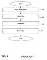
- Conventional manufacturing methodsinclude fabrication, wafer sort or probing, assembly or packaging, and testing performed in sequence.
- the fabrication operation 102forms the individual dies onto a semiconductor wafer.
- the waferis often 300 mm or more in diameter and typically includes a large number of integrated circuits or dies on the wafer. For example, a single wafer may produce 50 to 200 or more identical integrated circuit dies.
- Each of the individual diesis then tested to determine its operability, that is, to determine if the chips function in accordance with the design.
- This stepis typically performed at wafer sort or probe 104 .
- the wafer proberusually involves a material handling system to transfer wafers from their carriers to a flat chuck and aligns them precisely under a set of fine contacts or probe tips on a probe card.
- the probe cardprovides interconnection between the die pads and a load card which is connected to automated test equipment (ATE).
- ATEautomated test equipment
- the probe cardthus acts as an interface between the metallic pads on the dies and provides connections to the tester.
- the functional tester or automatic test equipment (ATE)is capable of functionally exercising all of the chip's designed features under software control. Any failure to meet the published specification is identified by the tester and the device is cataloged as a reject. Thus, both good and bad dies may be determined. Bad dies are often marked by either a probe or ink mark at the wafer sort operation.
- the assembly of the chipstakes place.
- the waferis diced, i.e., sawn along “streets” of the wafer to form individual die.
- the “streets” or scribe lineslie between each die and are used as cutting lines during the wafer sawing operation.
- the dieis separated from the wafer and packaged to form a device that can be attached and electrically connected to a printed circuit board, for example.
- the assembly operationincludes a number of sub-steps such as wafer sawing, die attachment, and bonding.
- a final opportunityis presented to test the functioning of the chips (die). This is also referred to as final test.
- a material handling systemtransfers packaged dies from their carriers and loads them into contacts or sockets on a load board.
- the functional tester or automatic test equipment (ATE)then functionally exercises the chip's designed features under software control to identify defective die.
- the wafer probe operationis a very delicate and time consuming operation requiring a great deal of skill.
- electrical contacts between the metallic pads on the dies positioned on the wafer and the testeris achieved by using a probe card.
- the probe cardis a customized printed circuit board designed to match the bonding pad geometry of each die and connect it to the test equipment. The wafer can then be moved either manually or automatically by the machine in both vertical and horizontal directions.
- the probe cardincludes thin metal probes which make the connection between the card's circuit, i.e., the printed circuit board portion of the probe card, and the die bonding pads. By lowering these probes onto the metallic contact pads of each die, an electrical connection is made for functionally exercising the die under a test program generated by the tester. Since probe cards must be custom built for each new integrated circuit design to match the particular metallic pad configuration for that design, expenditures for probe cards can be substantial. For example, at the time of the drafting of this specification, probe cards costs are as much as eighty thousand dollars or higher.
- test fixturessuch as probe cards
- ASICApplication-Specific Integrated Circuit
- the total anticipated production volume of the ASICmay be only a few thousand units. If the expected yield at wafer probe is on the order of ninety percent, it would make far more sense to skip the wafer probe test step entirely in favor of testing the die in its packaged form.
- the functioning of the diemay be performed at the final test step.
- Final testingdoes not require the dedicated, custom fixtures such as probe cards for testing, since many designs which are quite different in die form may still share the same package and the same arrangement of power and ground planes in the package.
- skipping the wafer sort stepresults in the loss of information regarding the original location of the die a particular wafer. For example, it is quite common to have ‘rogue’ wafers appearing from time to time in an otherwise normal wafer lot. A rogue wafer might yield very poorly at the wafer probe step, i.e., falling far outside the specifications due to a process irregularity, and might result in a decision that the entire wafer represents a process excursion that should be completely contained and not shipped to the customer. But if the wafer sort step was skipped, such information pertinent to all of the dies on the wafer would not otherwise be available at the final test step. That is, a slightly depressed yield at final test will not provide sufficient information to determine that all units built from a given wafer should be rejected, even if individual package die could be correlated to a particular wafer.
- the present inventionprovides methods for detecting fabrication defects in devices.
- a generic test interfacesuch as a variation of an electrical testing structure (i.e., e-test) probe card, the test fixture interface configured to provide electrical contact with pads and other contacts on the wafer.
- Datasuch as an identification number for the device can be thus monitored at the same time that the e-test structures located in the scribe streets are accessed.
- an electrical parameter for the integrated circuit diesuch as a supply current from a reference test cell located within the integrated circuit can also be monitored using the generic interface.
- statistical post processingcan be performed to identify wafer defect patterns.
- a method of manufacturing a semiconductor integrated circuitis provided.
- a wafer having a plurality of integrated circuit diesis provided.
- a standardized test fixturecontacts selected pads on the die positioned in a standardized location for determining a unique identification number for the die and for testing a parameter of the circuit.
- the test fixturealso provides electrical contact with electrical testing structures (e-test) located in a scribe line adjacent to the die.
- the contacts on the die used in the testare located in a standardized geometric location relative to the electrical testing structures located in the scribe line.
- the electrical parameterincludes one of supply voltage and current.
- the identification number and location data pertaining to the integrated circuit dieare used in post processing steps to identify defects in the plurality of dies and the patterns of the defects.
- a standardized test fixtureincludes probe tips positioned in standardized locations for obtaining identifier and Idd current measurements for a family of integrated circuits.
- a first group of the plurality of padscomprises pads connected to an identification cell located within an integrated circuit die on the wafer and a second group of the plurality of pads is connected to an electrical testing structure located in a scribe line adjacent to the die.
- the plurality of padsare located in a corner of the integrated circuit die adjacent to the location of electrical testing structure located in a scribe line adjacent to the die.
- a third group of the plurality of padsis connected to a reference test cell located on the integrated circuit die and configured to measure an electrical parameter for the integrated circuit.
- the method of manufacturing a semiconductor integrated circuitincludes providing a plurality of integrated circuit dies on a wafer. An identification number is generated from an identification cell located on each of the plurality of dies. The identification number is monitored before separating the plurality of dies from the wafer by using a generic interface configured to access pads over a plurality of different integrated circuit designs. The monitored identification number is used in statistical post processing to identify defects in any of the plurality of dies.
- the test fixtureprovides removable contact with pads at uniform locations on the dies. The fixture also provides access to electrical testing structures located on scribe lines of the wafer. The pads are located at a constant geometric relationship with the E-test pads to obtain at least one of a unique identifier for the die and a test parameter while accessing e-test information.
- FIG. 1is a flowchart illustrating conventional steps in the manufacturing of a semiconductor integrated circuit.
- FIG. 2Ais a diagram of a wafer configured with pads in standardized locations in accordance with one embodiment of the present invention.
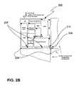
- FIG. 2Bis an expanded view of a die located on the wafer depicted in FIG. 2A , in accordance with one embodiment of the present invention.
- FIG. 3is a diagram of a test fixture in accordance with one embodiment of the present invention.
- FIG. 4is a diagram illustrating a configuration of the metallic pads of a wafer in accordance with one embodiment of the present invention.
- FIG. 5is a flowchart illustrating steps in the manufacturing of a semiconductor integrated circuit in accordance with one embodiment of the present invention.
- a method of manufacturing a semiconductor integrated circuitincludes providing a wafer having a plurality of dies formed on the wafer.
- the unencapsulated dieincludes at least one I.D. (identification) cell in the active die portion of the wafer.
- Pads for providing electrical connection to the circuitry of the dieare positioned in a standard position on the die.
- the dieis tested by applying a standard test fixture configured with contacts to provide electrical connection from the metallic pads on the die to the tester.
- the test fixtureis a generic probe card, configured with probe tips to match the standard positions of die pads connected to ID cells and other test cells on the die.
- FIG. 2Ais a diagram of a wafer configured with pads in standardized locations in accordance with one embodiment of the present invention.
- the semiconductor wafer 200includes a plurality of dies 202 , separated by scribe lines or streets 204 .
- One method of determining whether the process parameters fall within the accepted limitsis to run verification tests, commonly referred to as E-tests. Accordingly, the wafer 200 includes E-test circuitry and pads 206 located within the street.
- FIG. 2Bis an expanded view of a die located on the wafer depicted in FIG. 2A , in accordance with one embodiment of the present invention.
- the die 202is illustrated as including a number of functional blocks, for example, a microprocessor, RAM, numeric co-processor and graphics processor, all of which are intended to be illustrative but not limiting as to the variety of functional circuits which may be found on a typical integrated circuit.
- Included within the dieis a chip ID cell 210 and IDD reference cells 208 .
- the ID cell 210is configured to generate a random identifying number for each die on each wafer.
- the identifieris configured to generate sufficient bits (i.e., enough digits) so that the chance of an accidental duplication of two IDs during the manufacture of a large lot, for example ten million dies, will be remote.
- Suitable identifiersare commercially available, for example including the integrated circuit identification device disclosed in further detail in U.S. Pat. No. 6,161,213, issued to Lofstrom, which application is herein incorporated by reference in its entirety for all purposes.
- the integrated circuit identification device described in the Lofstrom patentis described as an array of electronic cells in which the magnitude of the output signal of each cell is a function of randomly occurring parametric variations from cell to cell.
- the integrated circuit identification device described therein as well as others commercially availableare believed to be suitable for use with the methods and test apparatus described herein. For this reason, further description of identifier cells here is deemed unnecessary.
- the diemay be traced through the manufacturing flow up to (or even beyond) the point that it ships to the customer. This provides identification information which may be correlated with measured data, such as performance data, which can be evaluated in statistical post-processing steps.
- Semiconductor manufacturingtypically performs end of line testing on completed wafers to evaluate die, for example to make decisions about evolving changes in the process and to improve yields. These tests include electrical or E-tests, designed to report parametric information about devices on the scribe line structures, i.e., the E-test structures.
- E-testsdesigned to report parametric information about devices on the scribe line structures, i.e., the E-test structures.
- certain areas of the scribe lines of each waferare reserved for special circuits to perform the e-tests. This special circuitry includes transistors of known dimensions. Extremely precise analog tests are typically performed on these transistors and the results analyzed to provide control of the fabrication process.
- e-test structuresare not typically needed for subsequent manufacturing steps once the necessary e-test information is extracted. For this reason the e-test structures are usually placed in the ‘scribe street’ between dice, a region which is destroyed when the wafer is sawed up into separate dice.
- the structures in the scribe streetare unpassivated or unencapsulated (not covered with a protective insulating layer), and they are tested conventionally with a dedicated probe card.
- Embodiments of the present inventionprovide a means for extracting the device ID (and similar information), without the necessity for a customized probe card or performing conventional wafer sort steps.
- the device ID informationis extracted during the electrical testing (E-testing) of the device.
- the wafer of a preferred embodimentincludes E-test structures 206 positioned within the scribe lines 204 of the wafer.
- the preferred embodimentis further configured such that, selected signals, for example relating to the ID cell and other selected parameters, are made available at fixed geometric positions relative to the signals already used for E-testing. That is, by direct placement of the identifier cell 210 in a predetermined location or by the routing of the necessary signals from the identifier cell to the pads in the predetermined location, the identifier information may be extracted at the E-test step, instead of at wafer sort. Thus, large investments in wafer sort hardware on low volume products can be avoided.
- the chip ID cell 210is located in a corner of the die adjacent to the locations of the E-test structures 206 .
- signals corresponding to a chip ID cellare made available at pads positioned in a corner of the die adjacent to the E-test structures 206 .
- the diewill include pads to provide signals that correspond to a parameter being tested.
- IDD reference cellsmay be positioned on the die to provide an indication of a supply current in a selected portion of the die.
- IDD reference cells 208examples include Suitable sample locations for IDD reference cells 208 .
- the IDD reference cells 208preferably are not positioned entirely in one corner of the die. That is, more effective readings are obtained if the IDD reference cells 208 are distributed evenly across the die as shown above.
- the IDD reference cellshave been provided as illustrative of a test reference cell and are not intended to be limiting. For example, other test parameters such as Vdd, may be obtained using appropriate test cells.
- the few signals needed to drive the IDD reference cellare easily routed and concentrated in the corner area shown, such that they may be driven at E-test at the same time that the E-test data is collected.
- the identifier information for the dieis preferably powered and collected through the interface of the E-test structure.
- the pads for the silicon ID signals and the reference IDD signalsare not positioned in the scribe street but instead are preferably positioned close physically to the scribe street.
- Thisenables the E-test probe card to be configured with extra pins needed to support these two functional blocks of on-chip circuitry. Modifications to existing reticle databases to accommodate these changes are believed to be minimal. While it is recognized that e-test structures have in some cases been limited to one structure per reticle exposure, changes to a single E-test pattern for each die being tested is expected to be easily accomplished. Such a change would entail only a one-time change in the process reticle database, and as such would be easily amortized over all designs built on that process.
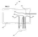
- FIG. 3is a diagram of a test fixture in accordance with one embodiment of the present invention.
- the test fixture 300includes a ring 312 provided for maintaining the probe tips 304 , 306 , 308 , 310 and 311 in a predetermined position relative to standardized positions of the corresponding pads on the wafer.
- Each of the probe tipsis attached to the end of a probe 303 , the probes being attached to the ring 312 , for example by using a conventional adhesive such as epoxy.
- the test fixture of the embodiment of the present inventionis formed in accordance with conventional techniques for the formation of probe cards except for the configuration of the probe tips. Methods of manufacturing probe cards are well known to those of skill in the art and thus further description of the basic steps is deemed unnecessary here.
- the probe tipsare configured to conform to a standardized position of selected pads on the wafer, for example in a preferred embodiment, the pads for an ID cell, a test cell, and e-test structures.
- probe tips 304 and 310are configured to match positions of corresponding pads of e-test structures located in the scribe street whereas probe tips 306 and 308 are configured to match corresponding pads on the active die portion, for example to obtain identification data and a limited set of test parameters
- the probe tipsprovide electrical contact to at least an identifier cell so that the wafer probe step can be eliminated and the positioning of the die from a given wafer made available for final testing and statistical post processing.
- FIG. 4is a diagram illustrating a portion of a test fixture superimposed on the metallic pads of a wafer in accordance with one embodiment of the present invention.
- the techniques of the embodiments of the present inventionare intended to provide a universal test fixture having probe tips that can be used to provide electrical contact with a variety of designs of the integrated circuits comprising a die, each of the die having selected pads placed in a standardized position such that the test fixture may be used to perform preliminary tests and obtain identification data from the die.
- a probe 303 and probe tip 306are shown superimposed on the wafer 400 .
- Wafer 400includes active die portion 422 and scribe lines 420 .
- Pads 404 , 410 , and 411are shown located within the scribe lines 420 and correspond to the electrical test structures described above.
- Pads 406 and 408are shown located within the active die portion 422 and preferably provide electrical connection to an ID cell and a reference test cell such as an IDD monitor cell.
- the pads 406 and 408located within the active die portion 422 , provide a set of signals in a fixed geometric position relative to the E-test structure pads 404 , 410 , and 411 .
- each of the test pads 406 , 408are located at a fixed vertical distance 426 and horizontal distance 428 in accordance with a predetermined layout so that the test fixture (probe card) can be reused over many designs.
- identification data and at least a minimized set of data, for example I dd datacan be obtained with a standardized test fixture.
- Quiescent current or I ddqis the current required to power the CMOS integrated circuit after all logic transitions are made.
- the magnitude of I ddqis commonly very small.
- the quiescent currentis one or more orders of magnitude higher.
- the quiescent currentmay be used to discriminate between good and bad die.
- the quiescent currentis measured simultaneously with E-test parameters by accessing reference test cells.
- the performance test parameterse.g., current
- the identification dataare used in a post-processing step, i.e., after fabrication of the wafer is completed.
- the amount of test data available during the preliminary testingis limited by the number of pads configured to correspond to the test fixture as illustrated in FIG. 3 .
- Providing the pads in a fixed geometric relationship to the e-test padspermits the test fixture to be reusable over different designs.
- current probe cardsare typically customized for each new design, thus driving up costs.
- the padsare configured in a standard configuration to match the most cost effective hardware solution. It is recognized that over time this configuration may change and accordingly the scope of the invention is intended to extend to the evolutions of an initially selected standard configuration as well as variations in the standard configuration as required to meet hardware requirements or technology differences and advances.
- FIG. 5is a flowchart illustrating steps in the manufacturing of a semiconductor integrated circuit in accordance with one embodiment of the present invention.
- the individual diesare formed onto a semiconductor wafer.
- each of the e-test structuresis individually tested in step 504 to provide information for control of the fabrication process.
- the device I.D. data and reference test cell datais accessed, for example by allowing the fixture's probe tips to make electrical connection with unencapsulated pads on the wafer. This testing is performed before the individual dies are separated form the wafer.
- the device I.D. data and test cell datais accessed simultaneous with the acquisition of e-test structure data although the invention is not so limited. That is, the scope of the invention is intended to also include accessing I.D. and test cell data either immediately before or after acquisition of the e-test data.
- the unencapsulated pads located in standardized positions in the active portion of the die and the scribe linesare accessed without undertaking a full wafer probe. Access is provided between the test fixture which makes electrical contact with the pads and the tester, preferably automated test equipment (ATE).
- ATEautomated test equipment
- the test fixture of the present embodimentthus acts as an interface between the metallic pads on the dies and the scribe lines and provides connections to the tester.
- the functional tester or automatic test equipment (ATE)is capable of reading the device identification data and the test cell data. This data and the identification information is preferably stored in the tester for use during statistical post processing steps.
- the waferis assembled. Initially, the wafer is diced, i.e., sawn along “streets” of the wafer to form individual die.
- the “streets” or scribe lineslie between each die and are used as cutting lines during the wafer sawing operation.
- the dieis separated from the wafer and packaged to form a device that can be attached and electrically connected to a printed circuit board, for example.
- the assembly operationincludes a number of sub-steps such as wafer sawing, die attachment, and bonding.
- the die functioning and other testingis performed.
- a material handling systemtransfers packaged dies from their carriers, loads them into contacts or sockets on a load board.
- the functional tester or automatic test equipment (ATE)then functionally exercises the chip's designed features under software control to identify defective die.
- the correlated identification data and test data obtained simultaneously with the E-testingis used to determine device defects.
- the identifier informationmay be used to trace die back to a particular wafer and to identify all dies from a particular wafer or production run as defective.
- the identification numberis generated and read, as in step 506 , the die's identification number is correlated with a physical location of the die an a particular wafer.
- the correlated informationis used to determine a wafer defect pattern. That is, post processing is used to determine chips that deviate from an expected distribution and using the deviation information and the fabricated location of dies on the wafer to predict other dies that are expected to be defective.
- the throughput of the testing processmay be may be increased while decreasing costs.
Landscapes
- Engineering & Computer Science (AREA)
- Manufacturing & Machinery (AREA)
- Computer Hardware Design (AREA)
- Microelectronics & Electronic Packaging (AREA)
- Power Engineering (AREA)
- Automation & Control Theory (AREA)
- Testing Or Measuring Of Semiconductors Or The Like (AREA)
Abstract
Description
Claims (24)
Priority Applications (1)
| Application Number | Priority Date | Filing Date | Title |
|---|---|---|---|
| US10/701,328US6939727B1 (en) | 2003-11-03 | 2003-11-03 | Method for performing statistical post processing in semiconductor manufacturing using ID cells |
Applications Claiming Priority (1)
| Application Number | Priority Date | Filing Date | Title |
|---|---|---|---|
| US10/701,328US6939727B1 (en) | 2003-11-03 | 2003-11-03 | Method for performing statistical post processing in semiconductor manufacturing using ID cells |
Publications (1)
| Publication Number | Publication Date |
|---|---|
| US6939727B1true US6939727B1 (en) | 2005-09-06 |
Family
ID=34886435
Family Applications (1)
| Application Number | Title | Priority Date | Filing Date |
|---|---|---|---|
| US10/701,328Expired - Fee RelatedUS6939727B1 (en) | 2003-11-03 | 2003-11-03 | Method for performing statistical post processing in semiconductor manufacturing using ID cells |
Country Status (1)
| Country | Link |
|---|---|
| US (1) | US6939727B1 (en) |
Cited By (15)
| Publication number | Priority date | Publication date | Assignee | Title |
|---|---|---|---|---|
| US20040138846A1 (en)* | 2001-05-24 | 2004-07-15 | Buxton Paul M. | Methods and apparatus for data analysis |
| US20040267477A1 (en)* | 2001-05-24 | 2004-12-30 | Scott Michael J. | Methods and apparatus for data analysis |
| US20050085932A1 (en)* | 2003-08-25 | 2005-04-21 | Majid Aghababazadeh | Technique for evaluating a fabrication of a semiconductor component and wafer |
| US20050278597A1 (en)* | 2001-05-24 | 2005-12-15 | Emilio Miguelanez | Methods and apparatus for data analysis |
| US20060085771A1 (en)* | 2004-10-20 | 2006-04-20 | Lsi Logic Corporation | Method of screening ASIC defects using independent component analysis of quiescent current measurements |
| US20060085155A1 (en)* | 2001-05-24 | 2006-04-20 | Emilio Miguelanez | Methods and apparatus for local outlier detection |
| US20070007988A1 (en)* | 2003-04-10 | 2007-01-11 | Umc Japan | LSI inspection method and defect inspection data analysis apparatus |
| WO2007036867A2 (en) | 2005-09-27 | 2007-04-05 | Nxp B.V. | Wafer with scribe lanes comprising external pads and/or active circuits for die testing |
| US20070219741A1 (en)* | 2005-05-20 | 2007-09-20 | Emilio Miguelanez | Methods and apparatus for hybrid outlier detection |
| US20070264729A1 (en)* | 2006-05-10 | 2007-11-15 | Anderson Brent A | Method for reducing within chip device parameter variations |
| US20080091977A1 (en)* | 2004-04-02 | 2008-04-17 | Emilio Miguelanez | Methods and apparatus for data analysis |
| US7437271B2 (en) | 2003-02-14 | 2008-10-14 | Test Advantage, Inc. | Methods and apparatus for data analysis |
| WO2012045202A1 (en)* | 2010-10-04 | 2012-04-12 | Sandisk Semiconductor (Shanghai) Co., Ltd. | Discrete component backward traceability and semiconductor device forward traceability |
| CN104022058A (en)* | 2010-10-04 | 2014-09-03 | 晟碟半导体(上海)有限公司 | Discrete assembly backward traceability and semiconductor device forward traceability |
| US10707138B1 (en)* | 2017-03-29 | 2020-07-07 | Xilinx, Inc. | High yield package assembly technique |
Citations (4)
| Publication number | Priority date | Publication date | Assignee | Title |
|---|---|---|---|---|
| US5206171A (en)* | 1990-12-17 | 1993-04-27 | Her Majesty The Queen In Right Of Canada | Programmable automated inoculator/replicator |
| US5557573A (en)* | 1995-08-21 | 1996-09-17 | Sgs-Thomson Microelectronics, Inc. | Entire wafer stress test method for integrated memory devices and circuit therefor |
| US6161213A (en) | 1999-02-17 | 2000-12-12 | Icid, Llc | System for providing an integrated circuit with a unique identification |
| US6714031B2 (en)* | 2001-05-31 | 2004-03-30 | Seiko Epson Corporation | Semiconductor device for wafer examination |
- 2003
- 2003-11-03USUS10/701,328patent/US6939727B1/ennot_activeExpired - Fee Related
Patent Citations (4)
| Publication number | Priority date | Publication date | Assignee | Title |
|---|---|---|---|---|
| US5206171A (en)* | 1990-12-17 | 1993-04-27 | Her Majesty The Queen In Right Of Canada | Programmable automated inoculator/replicator |
| US5557573A (en)* | 1995-08-21 | 1996-09-17 | Sgs-Thomson Microelectronics, Inc. | Entire wafer stress test method for integrated memory devices and circuit therefor |
| US6161213A (en) | 1999-02-17 | 2000-12-12 | Icid, Llc | System for providing an integrated circuit with a unique identification |
| US6714031B2 (en)* | 2001-05-31 | 2004-03-30 | Seiko Epson Corporation | Semiconductor device for wafer examination |
Cited By (49)
| Publication number | Priority date | Publication date | Assignee | Title |
|---|---|---|---|---|
| US8417477B2 (en) | 2001-05-24 | 2013-04-09 | Test Acuity Solutions, Inc. | Methods and apparatus for local outlier detection |
| US20040267477A1 (en)* | 2001-05-24 | 2004-12-30 | Scott Michael J. | Methods and apparatus for data analysis |
| US20050278597A1 (en)* | 2001-05-24 | 2005-12-15 | Emilio Miguelanez | Methods and apparatus for data analysis |
| US20080249742A1 (en)* | 2001-05-24 | 2008-10-09 | Scott Michael J | Methods and apparatus for data analysis |
| US20060085155A1 (en)* | 2001-05-24 | 2006-04-20 | Emilio Miguelanez | Methods and apparatus for local outlier detection |
| US8000928B2 (en) | 2001-05-24 | 2011-08-16 | Test Advantage, Inc. | Methods and apparatus for data analysis |
| US7395170B2 (en) | 2001-05-24 | 2008-07-01 | Test Advantage, Inc. | Methods and apparatus for data analysis |
| US7356430B2 (en) | 2001-05-24 | 2008-04-08 | Test Advantage, Inc. | Methods and apparatus for data analysis |
| US20040138846A1 (en)* | 2001-05-24 | 2004-07-15 | Buxton Paul M. | Methods and apparatus for data analysis |
| US7225107B2 (en) | 2001-05-24 | 2007-05-29 | Test Advantage, Inc. | Methods and apparatus for data analysis |
| US7437271B2 (en) | 2003-02-14 | 2008-10-14 | Test Advantage, Inc. | Methods and apparatus for data analysis |
| US20070007988A1 (en)* | 2003-04-10 | 2007-01-11 | Umc Japan | LSI inspection method and defect inspection data analysis apparatus |
| US7279923B2 (en)* | 2003-04-10 | 2007-10-09 | Umc Japan | LSI inspection method and defect inspection data analysis apparatus |
| US7730434B2 (en)* | 2003-08-25 | 2010-06-01 | Tau-Metrix, Inc. | Contactless technique for evaluating a fabrication of a wafer |
| US20100304509A1 (en)* | 2003-08-25 | 2010-12-02 | Majid Aghababazadeh | Contactless technique for evaluating a fabrication of a wafer |
| US20070236232A1 (en)* | 2003-08-25 | 2007-10-11 | Majid Aghababazadeh | System and apparatus for using test structures inside of a chip during the fabrication of the chip |
| US8344745B2 (en) | 2003-08-25 | 2013-01-01 | Tau-Metrix, Inc. | Test structures for evaluating a fabrication of a die or a wafer |
| US7723724B2 (en) | 2003-08-25 | 2010-05-25 | Tau-Metrix, Inc. | System for using test structures to evaluate a fabrication of a wafer |
| US7605597B2 (en) | 2003-08-25 | 2009-10-20 | Tau-Metrix, Inc. | Intra-chip power and test signal generation for use with test structures on wafers |
| US20080100319A1 (en)* | 2003-08-25 | 2008-05-01 | Majid Aghababazadeh | Intra-chip power and test signal generation for use with test structures on wafers |
| US8990759B2 (en) | 2003-08-25 | 2015-03-24 | Tau-Metrix, Inc. | Contactless technique for evaluating a fabrication of a wafer |
| US20070238206A1 (en)* | 2003-08-25 | 2007-10-11 | Majid Aghababazadeh | System and apparatus for using test structures inside of a chip during the fabrication of the chip |
| US7736916B2 (en) | 2003-08-25 | 2010-06-15 | Tau-Metrix, Inc. | System and apparatus for using test structures inside of a chip during the fabrication of the chip |
| US20070004063A1 (en)* | 2003-08-25 | 2007-01-04 | Majid Aghababazadeh | Technique for evaluating a fabrication of a die and wafer |
| US20050085932A1 (en)* | 2003-08-25 | 2005-04-21 | Majid Aghababazadeh | Technique for evaluating a fabrication of a semiconductor component and wafer |
| US20080315196A1 (en)* | 2003-08-25 | 2008-12-25 | Majid Aghababazadeh | Technique for evaluating a fabrication of a die and wafer |
| US20080091977A1 (en)* | 2004-04-02 | 2008-04-17 | Emilio Miguelanez | Methods and apparatus for data analysis |
| US7904279B2 (en) | 2004-04-02 | 2011-03-08 | Test Advantage, Inc. | Methods and apparatus for data analysis |
| US20060085771A1 (en)* | 2004-10-20 | 2006-04-20 | Lsi Logic Corporation | Method of screening ASIC defects using independent component analysis of quiescent current measurements |
| US7171638B2 (en)* | 2004-10-20 | 2007-01-30 | Lsi Logic Corporation | Methods of screening ASIC defects using independent component analysis of quiescent current measurements |
| US20070219741A1 (en)* | 2005-05-20 | 2007-09-20 | Emilio Miguelanez | Methods and apparatus for hybrid outlier detection |
| US8173448B2 (en)* | 2005-09-27 | 2012-05-08 | Nxp B.V. | Wafer with scribe lanes comprising external pads and/or active circuits for die testing |
| CN101273454B (en)* | 2005-09-27 | 2010-06-23 | Nxp股份有限公司 | Wafer with elements for die testing in scribe lanes |
| US20090127553A1 (en)* | 2005-09-27 | 2009-05-21 | Nxp B.V. | Wafer with scribe lanes comprising external pads and/or active circuits for die testing |
| WO2007036867A2 (en) | 2005-09-27 | 2007-04-05 | Nxp B.V. | Wafer with scribe lanes comprising external pads and/or active circuits for die testing |
| WO2007036867A3 (en)* | 2005-09-27 | 2007-07-19 | Nxp Bv | Wafer with scribe lanes comprising external pads and/or active circuits for die testing |
| US20070264729A1 (en)* | 2006-05-10 | 2007-11-15 | Anderson Brent A | Method for reducing within chip device parameter variations |
| US7541613B2 (en) | 2006-05-10 | 2009-06-02 | International Business Machines Corporation | Methods for reducing within chip device parameter variations |
| US7393703B2 (en)* | 2006-05-10 | 2008-07-01 | International Business Machines Corporation | Method for reducing within chip device parameter variations |
| US20080246097A1 (en)* | 2006-05-10 | 2008-10-09 | Brent Alan Anderson | Methods for reducing within chip device parameter variations |
| WO2012045202A1 (en)* | 2010-10-04 | 2012-04-12 | Sandisk Semiconductor (Shanghai) Co., Ltd. | Discrete component backward traceability and semiconductor device forward traceability |
| CN102640253A (en)* | 2010-10-04 | 2012-08-15 | 晟碟半导体(上海)有限公司 | Discrete component backward traceability and semiconductor device forward traceability |
| CN102640253B (en)* | 2010-10-04 | 2014-06-18 | 晟碟半导体(上海)有限公司 | Discrete component backward traceability and semiconductor device forward traceability |
| CN104022058A (en)* | 2010-10-04 | 2014-09-03 | 晟碟半导体(上海)有限公司 | Discrete assembly backward traceability and semiconductor device forward traceability |
| TWI459533B (en)* | 2010-10-04 | 2014-11-01 | Sandisk Semiconductor Shanghai Co Ltd | System and method for tracking semiconductor packages |
| KR20160034423A (en)* | 2010-10-04 | 2016-03-29 | 샌디스크 세미컨덕터 (상하이) 컴퍼니, 리미티드 | A semiconductor device and electronic device with discrete component backward traceability and forward traceability |
| TWI570874B (en)* | 2010-10-04 | 2017-02-11 | 晟碟半導體(上海)有限公司 | System and method for tracking semiconductor packages |
| US10229886B2 (en) | 2010-10-04 | 2019-03-12 | Sandisk Semiconductor (Shanghai) Co. Ltd. | Discrete component backward traceability and semiconductor device forward traceability |
| US10707138B1 (en)* | 2017-03-29 | 2020-07-07 | Xilinx, Inc. | High yield package assembly technique |
Similar Documents
| Publication | Publication Date | Title |
|---|---|---|
| US6939727B1 (en) | Method for performing statistical post processing in semiconductor manufacturing using ID cells | |
| CN100390554C (en) | Chip test solution reduced at wafer level | |
| KR100466984B1 (en) | Integrated circuit chip having test element group circuit and method of test the same | |
| US7054705B2 (en) | Method of manufacturing semiconductor devices | |
| US7719301B2 (en) | Testing method of semiconductor integrated circuit and information recording medium | |
| CN114152858A (en) | Electrical test device and test method for cutting channel device | |
| KR100487658B1 (en) | Probe needle cleaning apparatus and the method | |
| JP2007049161A (en) | Donut type parallel probe card and wafer inspection method using the same | |
| JP2003282654A (en) | Method for manufacturing semiconductor device | |
| US6429677B1 (en) | Method and apparatus for characterization of gate dielectrics | |
| JPH09115972A (en) | Array for testing of semiconductor element and test method | |
| US6940299B1 (en) | Method of testing for short circuits between adjacent input/output pins of an integrated circuit | |
| US6710616B1 (en) | Wafer level dynamic burn-in | |
| US8890557B2 (en) | Built-in self-test method and structure | |
| JP7370182B2 (en) | Semiconductor device and its inspection method | |
| US7285973B1 (en) | Methods for standardizing a test head assembly | |
| US20060186907A1 (en) | Method and apparatus for semiconductor testing utilizing dies with integrated circuit | |
| JP3865185B2 (en) | Semiconductor device, test apparatus and test method thereof | |
| KR100787742B1 (en) | Probe card recognition device and probe card recognition method using same | |
| KR0127639B1 (en) | Probing test method and apparatus | |
| JP2001141789A (en) | Semiconductor and non-defective / defective device for the semiconductor | |
| JP2013115217A (en) | Wafer inspection device and inspection method | |
| JP2002156404A (en) | Semiconductor measuring method and semiconductor measuring device | |
| KR100641471B1 (en) | Input IC structure of semiconductor device | |
| JP4137082B2 (en) | Semiconductor device testing equipment |
Legal Events
| Date | Code | Title | Description |
|---|---|---|---|
| AS | Assignment | Owner name:LSI LOGIC CORPORATION, CALIFORNIA Free format text:ASSIGNMENT OF ASSIGNORS INTEREST;ASSIGNORS:ALLEN, ERNEST, III;CASTANEDA, DAVID;LOOI, MIAW;REEL/FRAME:014667/0585 Effective date:20031031 | |
| FEPP | Fee payment procedure | Free format text:PAYOR NUMBER ASSIGNED (ORIGINAL EVENT CODE: ASPN); ENTITY STATUS OF PATENT OWNER: LARGE ENTITY | |
| FPAY | Fee payment | Year of fee payment:4 | |
| FPAY | Fee payment | Year of fee payment:8 | |
| AS | Assignment | Owner name:DEUTSCHE BANK AG NEW YORK BRANCH, AS COLLATERAL AG Free format text:PATENT SECURITY AGREEMENT;ASSIGNORS:LSI CORPORATION;AGERE SYSTEMS LLC;REEL/FRAME:032856/0031 Effective date:20140506 | |
| AS | Assignment | Owner name:LSI CORPORATION, CALIFORNIA Free format text:CHANGE OF NAME;ASSIGNOR:LSI LOGIC CORPORATION;REEL/FRAME:033102/0270 Effective date:20070406 | |
| AS | Assignment | Owner name:AVAGO TECHNOLOGIES GENERAL IP (SINGAPORE) PTE. LTD Free format text:ASSIGNMENT OF ASSIGNORS INTEREST;ASSIGNOR:LSI CORPORATION;REEL/FRAME:035390/0388 Effective date:20140814 | |
| AS | Assignment | Owner name:LSI CORPORATION, CALIFORNIA Free format text:TERMINATION AND RELEASE OF SECURITY INTEREST IN PATENT RIGHTS (RELEASES RF 032856-0031);ASSIGNOR:DEUTSCHE BANK AG NEW YORK BRANCH, AS COLLATERAL AGENT;REEL/FRAME:037684/0039 Effective date:20160201 Owner name:AGERE SYSTEMS LLC, PENNSYLVANIA Free format text:TERMINATION AND RELEASE OF SECURITY INTEREST IN PATENT RIGHTS (RELEASES RF 032856-0031);ASSIGNOR:DEUTSCHE BANK AG NEW YORK BRANCH, AS COLLATERAL AGENT;REEL/FRAME:037684/0039 Effective date:20160201 | |
| AS | Assignment | Owner name:BANK OF AMERICA, N.A., AS COLLATERAL AGENT, NORTH CAROLINA Free format text:PATENT SECURITY AGREEMENT;ASSIGNOR:AVAGO TECHNOLOGIES GENERAL IP (SINGAPORE) PTE. LTD.;REEL/FRAME:037808/0001 Effective date:20160201 Owner name:BANK OF AMERICA, N.A., AS COLLATERAL AGENT, NORTH Free format text:PATENT SECURITY AGREEMENT;ASSIGNOR:AVAGO TECHNOLOGIES GENERAL IP (SINGAPORE) PTE. LTD.;REEL/FRAME:037808/0001 Effective date:20160201 | |
| AS | Assignment | Owner name:AVAGO TECHNOLOGIES GENERAL IP (SINGAPORE) PTE. LTD., SINGAPORE Free format text:TERMINATION AND RELEASE OF SECURITY INTEREST IN PATENTS;ASSIGNOR:BANK OF AMERICA, N.A., AS COLLATERAL AGENT;REEL/FRAME:041710/0001 Effective date:20170119 Owner name:AVAGO TECHNOLOGIES GENERAL IP (SINGAPORE) PTE. LTD Free format text:TERMINATION AND RELEASE OF SECURITY INTEREST IN PATENTS;ASSIGNOR:BANK OF AMERICA, N.A., AS COLLATERAL AGENT;REEL/FRAME:041710/0001 Effective date:20170119 | |
| REMI | Maintenance fee reminder mailed | ||
| LAPS | Lapse for failure to pay maintenance fees | Free format text:PATENT EXPIRED FOR FAILURE TO PAY MAINTENANCE FEES (ORIGINAL EVENT CODE: EXP.) | |
| STCH | Information on status: patent discontinuation | Free format text:PATENT EXPIRED DUE TO NONPAYMENT OF MAINTENANCE FEES UNDER 37 CFR 1.362 | |
| FP | Lapsed due to failure to pay maintenance fee | Effective date:20170906 | |
| AS | Assignment | Owner name:BELL SEMICONDUCTOR, LLC, ILLINOIS Free format text:ASSIGNMENT OF ASSIGNORS INTEREST;ASSIGNORS:AVAGO TECHNOLOGIES GENERAL IP (SINGAPORE) PTE. LTD.;BROADCOM CORPORATION;REEL/FRAME:044886/0001 Effective date:20171208 | |
| AS | Assignment | Owner name:CORTLAND CAPITAL MARKET SERVICES LLC, AS COLLATERA Free format text:SECURITY INTEREST;ASSIGNORS:HILCO PATENT ACQUISITION 56, LLC;BELL SEMICONDUCTOR, LLC;BELL NORTHERN RESEARCH, LLC;REEL/FRAME:045216/0020 Effective date:20180124 | |
| AS | Assignment | Owner name:BELL NORTHERN RESEARCH, LLC, ILLINOIS Free format text:SECURITY INTEREST;ASSIGNOR:CORTLAND CAPITAL MARKET SERVICES LLC;REEL/FRAME:060885/0001 Effective date:20220401 Owner name:BELL SEMICONDUCTOR, LLC, ILLINOIS Free format text:SECURITY INTEREST;ASSIGNOR:CORTLAND CAPITAL MARKET SERVICES LLC;REEL/FRAME:060885/0001 Effective date:20220401 Owner name:HILCO PATENT ACQUISITION 56, LLC, ILLINOIS Free format text:SECURITY INTEREST;ASSIGNOR:CORTLAND CAPITAL MARKET SERVICES LLC;REEL/FRAME:060885/0001 Effective date:20220401 |