US6939579B2 - ALD reactor and method with controlled wall temperature - Google Patents
ALD reactor and method with controlled wall temperatureDownload PDFInfo
- Publication number
- US6939579B2 US6939579B2US09/801,542US80154201AUS6939579B2US 6939579 B2US6939579 B2US 6939579B2US 80154201 AUS80154201 AUS 80154201AUS 6939579 B2US6939579 B2US 6939579B2
- Authority
- US
- United States
- Prior art keywords
- temperature
- substrate
- walls
- ald
- chamber
- Prior art date
- Legal status (The legal status is an assumption and is not a legal conclusion. Google has not performed a legal analysis and makes no representation as to the accuracy of the status listed.)
- Expired - Lifetime
Links
- 238000000034methodMethods0.000titleclaimsabstractdescription41
- 239000000758substrateSubstances0.000claimsabstractdescription174
- 238000006243chemical reactionMethods0.000claimsabstractdescription96
- 238000000231atomic layer depositionMethods0.000claimsabstractdescription91
- 230000012010growthEffects0.000claimsabstractdescription55
- 238000009833condensationMethods0.000claimsabstractdescription23
- 230000005494condensationEffects0.000claimsabstractdescription23
- 239000010408filmSubstances0.000claimsabstractdescription15
- 238000005979thermal decomposition reactionMethods0.000claimsabstractdescription15
- 239000010409thin filmSubstances0.000claimsabstractdescription12
- 238000004375physisorptionMethods0.000claimsabstractdescription7
- 239000000376reactantSubstances0.000claimsdescription71
- 239000012530fluidSubstances0.000claimsdescription39
- 238000000151depositionMethods0.000claimsdescription36
- 230000008021depositionEffects0.000claimsdescription36
- 238000010438heat treatmentMethods0.000claimsdescription13
- 239000012808vapor phaseSubstances0.000claimsdescription12
- XLYOFNOQVPJJNP-UHFFFAOYSA-NwaterSubstancesOXLYOFNOQVPJJNP-UHFFFAOYSA-N0.000claimsdescription12
- 239000002356single layerSubstances0.000claimsdescription9
- 238000011068loading methodMethods0.000claimsdescription5
- 238000006557surface reactionMethods0.000claims3
- 230000001105regulatory effectEffects0.000abstractdescription18
- 235000012431wafersNutrition0.000abstractdescription3
- 230000003134recirculating effectEffects0.000description24
- 239000000126substanceSubstances0.000description17
- 230000008569processEffects0.000description13
- 238000012546transferMethods0.000description10
- 238000001816coolingMethods0.000description9
- 239000007789gasSubstances0.000description9
- 238000013461designMethods0.000description8
- BPUBBGLMJRNUCC-UHFFFAOYSA-Noxygen(2-);tantalum(5+)Chemical group[O-2].[O-2].[O-2].[O-2].[O-2].[Ta+5].[Ta+5]BPUBBGLMJRNUCC-UHFFFAOYSA-N0.000description7
- PBCFLUZVCVVTBY-UHFFFAOYSA-Ntantalum pentoxideInorganic materialsO=[Ta](=O)O[Ta](=O)=OPBCFLUZVCVVTBY-UHFFFAOYSA-N0.000description7
- 239000006227byproductSubstances0.000description6
- 239000012634fragmentSubstances0.000description6
- 238000010926purgeMethods0.000description6
- XOLBLPGZBRYERU-UHFFFAOYSA-Ntin dioxideChemical compoundO=[Sn]=OXOLBLPGZBRYERU-UHFFFAOYSA-N0.000description6
- QGZKDVFQNNGYKY-UHFFFAOYSA-NAmmoniaChemical compoundNQGZKDVFQNNGYKY-UHFFFAOYSA-N0.000description5
- -1hydrogen halidesChemical class0.000description5
- 239000000463materialSubstances0.000description5
- 229910021627Tin(IV) chlorideInorganic materials0.000description4
- 230000008901benefitEffects0.000description4
- 238000005229chemical vapour depositionMethods0.000description4
- 239000010410layerSubstances0.000description4
- 229910052751metalInorganic materials0.000description4
- 239000002184metalSubstances0.000description4
- HPGGPRDJHPYFRM-UHFFFAOYSA-Jtin(iv) chlorideChemical compoundCl[Sn](Cl)(Cl)ClHPGGPRDJHPYFRM-UHFFFAOYSA-J0.000description4
- VEXZGXHMUGYJMC-UHFFFAOYSA-NHydrochloric acidChemical compoundClVEXZGXHMUGYJMC-UHFFFAOYSA-N0.000description3
- 229910004537TaCl5Inorganic materials0.000description3
- RTAQQCXQSZGOHL-UHFFFAOYSA-NTitaniumChemical compound[Ti]RTAQQCXQSZGOHL-UHFFFAOYSA-N0.000description3
- 230000001276controlling effectEffects0.000description3
- 239000013078crystalSubstances0.000description3
- 230000003247decreasing effectEffects0.000description3
- 238000003795desorptionMethods0.000description3
- 239000001257hydrogenSubstances0.000description3
- 229910052739hydrogenInorganic materials0.000description3
- 230000007246mechanismEffects0.000description3
- 239000002245particleSubstances0.000description3
- 230000009257reactivityEffects0.000description3
- OEIMLTQPLAGXMX-UHFFFAOYSA-Itantalum(v) chlorideChemical compoundCl[Ta](Cl)(Cl)(Cl)ClOEIMLTQPLAGXMX-UHFFFAOYSA-I0.000description3
- 239000010936titaniumSubstances0.000description3
- 229910052719titaniumInorganic materials0.000description3
- MHCVCKDNQYMGEX-UHFFFAOYSA-N1,1'-biphenyl;phenoxybenzeneChemical compoundC1=CC=CC=C1C1=CC=CC=C1.C=1C=CC=CC=1OC1=CC=CC=C1MHCVCKDNQYMGEX-UHFFFAOYSA-N0.000description2
- IJGRMHOSHXDMSA-UHFFFAOYSA-NAtomic nitrogenChemical compoundN#NIJGRMHOSHXDMSA-UHFFFAOYSA-N0.000description2
- GYHNNYVSQQEPJS-UHFFFAOYSA-NGalliumChemical compound[Ga]GYHNNYVSQQEPJS-UHFFFAOYSA-N0.000description2
- 238000009825accumulationMethods0.000description2
- 230000004913activationEffects0.000description2
- 229910021529ammoniaInorganic materials0.000description2
- 238000003877atomic layer epitaxyMethods0.000description2
- 230000015572biosynthetic processEffects0.000description2
- 229910052792caesiumInorganic materials0.000description2
- 238000011109contaminationMethods0.000description2
- 230000001419dependent effectEffects0.000description2
- USIUVYZYUHIAEV-UHFFFAOYSA-Ndiphenyl etherChemical compoundC=1C=CC=CC=1OC1=CC=CC=C1USIUVYZYUHIAEV-UHFFFAOYSA-N0.000description2
- 238000000407epitaxyMethods0.000description2
- 239000006023eutectic alloySubstances0.000description2
- 230000001747exhibiting effectEffects0.000description2
- 229910052733galliumInorganic materials0.000description2
- 125000002887hydroxy groupChemical group[H]O*0.000description2
- 239000011261inert gasSubstances0.000description2
- 239000003446ligandSubstances0.000description2
- 239000007788liquidSubstances0.000description2
- 229910001338liquidmetalInorganic materials0.000description2
- 229910001507metal halideInorganic materials0.000description2
- 150000005309metal halidesChemical class0.000description2
- 230000010355oscillationEffects0.000description2
- 229910052700potassiumInorganic materials0.000description2
- 238000012545processingMethods0.000description2
- 229910052701rubidiumInorganic materials0.000description2
- 229910052711seleniumInorganic materials0.000description2
- 239000011669seleniumSubstances0.000description2
- 229910052708sodiumInorganic materials0.000description2
- 239000007787solidSubstances0.000description2
- 239000011343solid materialSubstances0.000description2
- 238000001179sorption measurementMethods0.000description2
- 229910000807Ga alloyInorganic materials0.000description1
- 229910001218Gallium arsenideInorganic materials0.000description1
- CBENFWSGALASAD-UHFFFAOYSA-NOzoneChemical compound[O-][O+]=OCBENFWSGALASAD-UHFFFAOYSA-N0.000description1
- BUGBHKTXTAQXES-UHFFFAOYSA-NSeleniumChemical compound[Se]BUGBHKTXTAQXES-UHFFFAOYSA-N0.000description1
- ATJFFYVFTNAWJD-UHFFFAOYSA-NTinChemical compound[Sn]ATJFFYVFTNAWJD-UHFFFAOYSA-N0.000description1
- 229910000573alkali metal alloyInorganic materials0.000description1
- RBFQJDQYXXHULB-UHFFFAOYSA-NarsaneChemical compound[AsH3]RBFQJDQYXXHULB-UHFFFAOYSA-N0.000description1
- 239000002585baseSubstances0.000description1
- 238000004140cleaningMethods0.000description1
- 238000004891communicationMethods0.000description1
- 239000002826coolantSubstances0.000description1
- 238000000354decomposition reactionMethods0.000description1
- 238000009795derivationMethods0.000description1
- 238000010494dissociation reactionMethods0.000description1
- 230000005593dissociationsEffects0.000description1
- 238000005530etchingMethods0.000description1
- 239000000374eutectic mixtureSubstances0.000description1
- 239000013529heat transfer fluidSubstances0.000description1
- 239000001307heliumSubstances0.000description1
- 229910052734heliumInorganic materials0.000description1
- SWQJXJOGLNCZEY-UHFFFAOYSA-Nhelium atomChemical compound[He]SWQJXJOGLNCZEY-UHFFFAOYSA-N0.000description1
- 231100000086high toxicityToxicity0.000description1
- 229910052738indiumInorganic materials0.000description1
- APFVFJFRJDLVQX-UHFFFAOYSA-Nindium atomChemical compound[In]APFVFJFRJDLVQX-UHFFFAOYSA-N0.000description1
- 230000001939inductive effectEffects0.000description1
- 230000010354integrationEffects0.000description1
- 238000004519manufacturing processMethods0.000description1
- 239000000155meltSubstances0.000description1
- QSHDDOUJBYECFT-UHFFFAOYSA-NmercuryChemical compound[Hg]QSHDDOUJBYECFT-UHFFFAOYSA-N0.000description1
- 229910052753mercuryInorganic materials0.000description1
- 229910001510metal chlorideInorganic materials0.000description1
- 150000004767nitridesChemical class0.000description1
- 229910052757nitrogenInorganic materials0.000description1
- 229910000069nitrogen hydrideInorganic materials0.000description1
- 230000009972noncorrosive effectEffects0.000description1
- NJPPVKZQTLUDBO-UHFFFAOYSA-NnovaluronChemical compoundC1=C(Cl)C(OC(F)(F)C(OC(F)(F)F)F)=CC=C1NC(=O)NC(=O)C1=C(F)C=CC=C1FNJPPVKZQTLUDBO-UHFFFAOYSA-N0.000description1
- 239000012071phaseSubstances0.000description1
- 238000009428plumbingMethods0.000description1
- 229920001296polysiloxanePolymers0.000description1
- 238000005086pumpingMethods0.000description1
- 238000007789sealingMethods0.000description1
- SBIBMFFZSBJNJF-UHFFFAOYSA-Nselenium;zincChemical compound[Se]=[Zn]SBIBMFFZSBJNJF-UHFFFAOYSA-N0.000description1
- 229910052710siliconInorganic materials0.000description1
- 239000010703siliconSubstances0.000description1
- 239000005361soda-lime glassSubstances0.000description1
- 229910052715tantalumInorganic materials0.000description1
- 231100000331toxicToxicity0.000description1
- 230000002588toxic effectEffects0.000description1
- XCZXGTMEAKBVPV-UHFFFAOYSA-NtrimethylgalliumChemical compoundC[Ga](C)CXCZXGTMEAKBVPV-UHFFFAOYSA-N0.000description1
- 230000004222uncontrolled growthEffects0.000description1
- 229910052725zincInorganic materials0.000description1
Images


Classifications
- C—CHEMISTRY; METALLURGY
- C23—COATING METALLIC MATERIAL; COATING MATERIAL WITH METALLIC MATERIAL; CHEMICAL SURFACE TREATMENT; DIFFUSION TREATMENT OF METALLIC MATERIAL; COATING BY VACUUM EVAPORATION, BY SPUTTERING, BY ION IMPLANTATION OR BY CHEMICAL VAPOUR DEPOSITION, IN GENERAL; INHIBITING CORROSION OF METALLIC MATERIAL OR INCRUSTATION IN GENERAL
- C23C—COATING METALLIC MATERIAL; COATING MATERIAL WITH METALLIC MATERIAL; SURFACE TREATMENT OF METALLIC MATERIAL BY DIFFUSION INTO THE SURFACE, BY CHEMICAL CONVERSION OR SUBSTITUTION; COATING BY VACUUM EVAPORATION, BY SPUTTERING, BY ION IMPLANTATION OR BY CHEMICAL VAPOUR DEPOSITION, IN GENERAL
- C23C16/00—Chemical coating by decomposition of gaseous compounds, without leaving reaction products of surface material in the coating, i.e. chemical vapour deposition [CVD] processes
- C23C16/44—Chemical coating by decomposition of gaseous compounds, without leaving reaction products of surface material in the coating, i.e. chemical vapour deposition [CVD] processes characterised by the method of coating
- C23C16/455—Chemical coating by decomposition of gaseous compounds, without leaving reaction products of surface material in the coating, i.e. chemical vapour deposition [CVD] processes characterised by the method of coating characterised by the method used for introducing gases into reaction chamber or for modifying gas flows in reaction chamber
- C23C16/45523—Pulsed gas flow or change of composition over time
- C23C16/45525—Atomic layer deposition [ALD]
- C—CHEMISTRY; METALLURGY
- C23—COATING METALLIC MATERIAL; COATING MATERIAL WITH METALLIC MATERIAL; CHEMICAL SURFACE TREATMENT; DIFFUSION TREATMENT OF METALLIC MATERIAL; COATING BY VACUUM EVAPORATION, BY SPUTTERING, BY ION IMPLANTATION OR BY CHEMICAL VAPOUR DEPOSITION, IN GENERAL; INHIBITING CORROSION OF METALLIC MATERIAL OR INCRUSTATION IN GENERAL
- C23C—COATING METALLIC MATERIAL; COATING MATERIAL WITH METALLIC MATERIAL; SURFACE TREATMENT OF METALLIC MATERIAL BY DIFFUSION INTO THE SURFACE, BY CHEMICAL CONVERSION OR SUBSTITUTION; COATING BY VACUUM EVAPORATION, BY SPUTTERING, BY ION IMPLANTATION OR BY CHEMICAL VAPOUR DEPOSITION, IN GENERAL
- C23C16/00—Chemical coating by decomposition of gaseous compounds, without leaving reaction products of surface material in the coating, i.e. chemical vapour deposition [CVD] processes
- C23C16/22—Chemical coating by decomposition of gaseous compounds, without leaving reaction products of surface material in the coating, i.e. chemical vapour deposition [CVD] processes characterised by the deposition of inorganic material, other than metallic material
- C23C16/30—Deposition of compounds, mixtures or solid solutions, e.g. borides, carbides, nitrides
- C23C16/301—AIII BV compounds, where A is Al, Ga, In or Tl and B is N, P, As, Sb or Bi
- C—CHEMISTRY; METALLURGY
- C23—COATING METALLIC MATERIAL; COATING MATERIAL WITH METALLIC MATERIAL; CHEMICAL SURFACE TREATMENT; DIFFUSION TREATMENT OF METALLIC MATERIAL; COATING BY VACUUM EVAPORATION, BY SPUTTERING, BY ION IMPLANTATION OR BY CHEMICAL VAPOUR DEPOSITION, IN GENERAL; INHIBITING CORROSION OF METALLIC MATERIAL OR INCRUSTATION IN GENERAL
- C23C—COATING METALLIC MATERIAL; COATING MATERIAL WITH METALLIC MATERIAL; SURFACE TREATMENT OF METALLIC MATERIAL BY DIFFUSION INTO THE SURFACE, BY CHEMICAL CONVERSION OR SUBSTITUTION; COATING BY VACUUM EVAPORATION, BY SPUTTERING, BY ION IMPLANTATION OR BY CHEMICAL VAPOUR DEPOSITION, IN GENERAL
- C23C16/00—Chemical coating by decomposition of gaseous compounds, without leaving reaction products of surface material in the coating, i.e. chemical vapour deposition [CVD] processes
- C23C16/22—Chemical coating by decomposition of gaseous compounds, without leaving reaction products of surface material in the coating, i.e. chemical vapour deposition [CVD] processes characterised by the deposition of inorganic material, other than metallic material
- C23C16/30—Deposition of compounds, mixtures or solid solutions, e.g. borides, carbides, nitrides
- C23C16/305—Sulfides, selenides, or tellurides
- C—CHEMISTRY; METALLURGY
- C23—COATING METALLIC MATERIAL; COATING MATERIAL WITH METALLIC MATERIAL; CHEMICAL SURFACE TREATMENT; DIFFUSION TREATMENT OF METALLIC MATERIAL; COATING BY VACUUM EVAPORATION, BY SPUTTERING, BY ION IMPLANTATION OR BY CHEMICAL VAPOUR DEPOSITION, IN GENERAL; INHIBITING CORROSION OF METALLIC MATERIAL OR INCRUSTATION IN GENERAL
- C23C—COATING METALLIC MATERIAL; COATING MATERIAL WITH METALLIC MATERIAL; SURFACE TREATMENT OF METALLIC MATERIAL BY DIFFUSION INTO THE SURFACE, BY CHEMICAL CONVERSION OR SUBSTITUTION; COATING BY VACUUM EVAPORATION, BY SPUTTERING, BY ION IMPLANTATION OR BY CHEMICAL VAPOUR DEPOSITION, IN GENERAL
- C23C16/00—Chemical coating by decomposition of gaseous compounds, without leaving reaction products of surface material in the coating, i.e. chemical vapour deposition [CVD] processes
- C23C16/22—Chemical coating by decomposition of gaseous compounds, without leaving reaction products of surface material in the coating, i.e. chemical vapour deposition [CVD] processes characterised by the deposition of inorganic material, other than metallic material
- C23C16/30—Deposition of compounds, mixtures or solid solutions, e.g. borides, carbides, nitrides
- C23C16/40—Oxides
- C23C16/403—Oxides of aluminium, magnesium or beryllium
- C—CHEMISTRY; METALLURGY
- C23—COATING METALLIC MATERIAL; COATING MATERIAL WITH METALLIC MATERIAL; CHEMICAL SURFACE TREATMENT; DIFFUSION TREATMENT OF METALLIC MATERIAL; COATING BY VACUUM EVAPORATION, BY SPUTTERING, BY ION IMPLANTATION OR BY CHEMICAL VAPOUR DEPOSITION, IN GENERAL; INHIBITING CORROSION OF METALLIC MATERIAL OR INCRUSTATION IN GENERAL
- C23C—COATING METALLIC MATERIAL; COATING MATERIAL WITH METALLIC MATERIAL; SURFACE TREATMENT OF METALLIC MATERIAL BY DIFFUSION INTO THE SURFACE, BY CHEMICAL CONVERSION OR SUBSTITUTION; COATING BY VACUUM EVAPORATION, BY SPUTTERING, BY ION IMPLANTATION OR BY CHEMICAL VAPOUR DEPOSITION, IN GENERAL
- C23C16/00—Chemical coating by decomposition of gaseous compounds, without leaving reaction products of surface material in the coating, i.e. chemical vapour deposition [CVD] processes
- C23C16/22—Chemical coating by decomposition of gaseous compounds, without leaving reaction products of surface material in the coating, i.e. chemical vapour deposition [CVD] processes characterised by the deposition of inorganic material, other than metallic material
- C23C16/30—Deposition of compounds, mixtures or solid solutions, e.g. borides, carbides, nitrides
- C23C16/40—Oxides
- C23C16/405—Oxides of refractory metals or yttrium
- C—CHEMISTRY; METALLURGY
- C23—COATING METALLIC MATERIAL; COATING MATERIAL WITH METALLIC MATERIAL; CHEMICAL SURFACE TREATMENT; DIFFUSION TREATMENT OF METALLIC MATERIAL; COATING BY VACUUM EVAPORATION, BY SPUTTERING, BY ION IMPLANTATION OR BY CHEMICAL VAPOUR DEPOSITION, IN GENERAL; INHIBITING CORROSION OF METALLIC MATERIAL OR INCRUSTATION IN GENERAL
- C23C—COATING METALLIC MATERIAL; COATING MATERIAL WITH METALLIC MATERIAL; SURFACE TREATMENT OF METALLIC MATERIAL BY DIFFUSION INTO THE SURFACE, BY CHEMICAL CONVERSION OR SUBSTITUTION; COATING BY VACUUM EVAPORATION, BY SPUTTERING, BY ION IMPLANTATION OR BY CHEMICAL VAPOUR DEPOSITION, IN GENERAL
- C23C16/00—Chemical coating by decomposition of gaseous compounds, without leaving reaction products of surface material in the coating, i.e. chemical vapour deposition [CVD] processes
- C23C16/22—Chemical coating by decomposition of gaseous compounds, without leaving reaction products of surface material in the coating, i.e. chemical vapour deposition [CVD] processes characterised by the deposition of inorganic material, other than metallic material
- C23C16/30—Deposition of compounds, mixtures or solid solutions, e.g. borides, carbides, nitrides
- C23C16/40—Oxides
- C23C16/407—Oxides of zinc, germanium, cadmium, indium, tin, thallium or bismuth
- C—CHEMISTRY; METALLURGY
- C23—COATING METALLIC MATERIAL; COATING MATERIAL WITH METALLIC MATERIAL; CHEMICAL SURFACE TREATMENT; DIFFUSION TREATMENT OF METALLIC MATERIAL; COATING BY VACUUM EVAPORATION, BY SPUTTERING, BY ION IMPLANTATION OR BY CHEMICAL VAPOUR DEPOSITION, IN GENERAL; INHIBITING CORROSION OF METALLIC MATERIAL OR INCRUSTATION IN GENERAL
- C23C—COATING METALLIC MATERIAL; COATING MATERIAL WITH METALLIC MATERIAL; SURFACE TREATMENT OF METALLIC MATERIAL BY DIFFUSION INTO THE SURFACE, BY CHEMICAL CONVERSION OR SUBSTITUTION; COATING BY VACUUM EVAPORATION, BY SPUTTERING, BY ION IMPLANTATION OR BY CHEMICAL VAPOUR DEPOSITION, IN GENERAL
- C23C16/00—Chemical coating by decomposition of gaseous compounds, without leaving reaction products of surface material in the coating, i.e. chemical vapour deposition [CVD] processes
- C23C16/44—Chemical coating by decomposition of gaseous compounds, without leaving reaction products of surface material in the coating, i.e. chemical vapour deposition [CVD] processes characterised by the method of coating
- C23C16/455—Chemical coating by decomposition of gaseous compounds, without leaving reaction products of surface material in the coating, i.e. chemical vapour deposition [CVD] processes characterised by the method of coating characterised by the method used for introducing gases into reaction chamber or for modifying gas flows in reaction chamber
- C23C16/45523—Pulsed gas flow or change of composition over time
- C23C16/45525—Atomic layer deposition [ALD]
- C23C16/45544—Atomic layer deposition [ALD] characterized by the apparatus
- C—CHEMISTRY; METALLURGY
- C23—COATING METALLIC MATERIAL; COATING MATERIAL WITH METALLIC MATERIAL; CHEMICAL SURFACE TREATMENT; DIFFUSION TREATMENT OF METALLIC MATERIAL; COATING BY VACUUM EVAPORATION, BY SPUTTERING, BY ION IMPLANTATION OR BY CHEMICAL VAPOUR DEPOSITION, IN GENERAL; INHIBITING CORROSION OF METALLIC MATERIAL OR INCRUSTATION IN GENERAL
- C23C—COATING METALLIC MATERIAL; COATING MATERIAL WITH METALLIC MATERIAL; SURFACE TREATMENT OF METALLIC MATERIAL BY DIFFUSION INTO THE SURFACE, BY CHEMICAL CONVERSION OR SUBSTITUTION; COATING BY VACUUM EVAPORATION, BY SPUTTERING, BY ION IMPLANTATION OR BY CHEMICAL VAPOUR DEPOSITION, IN GENERAL
- C23C16/00—Chemical coating by decomposition of gaseous compounds, without leaving reaction products of surface material in the coating, i.e. chemical vapour deposition [CVD] processes
- C23C16/44—Chemical coating by decomposition of gaseous compounds, without leaving reaction products of surface material in the coating, i.e. chemical vapour deposition [CVD] processes characterised by the method of coating
- C23C16/46—Chemical coating by decomposition of gaseous compounds, without leaving reaction products of surface material in the coating, i.e. chemical vapour deposition [CVD] processes characterised by the method of coating characterised by the method used for heating the substrate
Definitions
- This inventionrelates to the field of reactor design for atomic layer deposition of thin films onto substrates such as wafers and flat panel displays.
- a substrate placed in a reaction spaceis subjected to alternating pulses of at least two different reactants suitable for producing a desired thin film on the substrate.
- ALDatomic layer deposition
- a monolayer of the first reactantis chemisorbed on the surface of the substrate until all of the available surface sites are occupied with an adsorbed portion of a reactant molecule and saturation occurs.
- the surface sitesmay be occupied by the whole of or by a fragment of a vapor-phase reactant molecule, such as when a metal chloride molecule chemisorbs on a surface site that has a hydroxyl group.
- TaCl 5may chemisorb as a TaCl 4 fragment, with HCl released as a gaseous byproduct.
- the reactionis chemically self-limiting because gaseous first reactant will not adsorb or react with the portion of the first reactant that has already been adsorbed on the substrate surface. The excess of the reactant is then removed by purging the reaction space with an inert gas and/or evacuating the reaction space.
- the substrateis exposed to a pulse of the second reactant, which chemically reacts with the adsorbed portion of the first reactant molecules until the reaction is complete and the surface is covered with a monolayer of the chemisorbed portion of the second reactant.
- Fragments of the second reactantwill be adsorbed under some reaction conditions. For example, when water is used as the second reactant it may leave a fragment of H 2 O, such as hydroxyl groups (—OH) on the surface. Similarly, when ammonia (NH 3 ) is used as the second reactant it may leave fragments such as NH or NH 2 groups on the surface. Reaction conditions such as temperature and pressure are chosen to ensure that physisorption of more than one monolayer of the first or second reactant (or portions thereof) on the substrate cannot occur. In this way the growth of the film proceeds atomic layer by atomic layer.
- the temperature of the substrateis not considered to be very critical because the growth rate of the film is not dependent on the temperature of the substrate but rather on the sequential exposure to the different reactant pulses.
- relative temperature independence of the processis a primary advantage of ALD, leading to perfect step-wise coverage despite temperature non-uniformities across large substrates.
- the temperatureis preferably high enough to prevent condensation of the reactants on the substrate and to allow the reaction to proceed at a sufficiently high rate.
- the substrate temperaturepreferably remains below the limit where thermal decomposition of the individual reactants occurs. For many combinations of reactants, such as metal halides and water, the reaction is able to proceed at temperatures as low as room temperature and as high as the thermal decomposition temperature limit for the reactants. Thus, a wide temperature window for atomic layer deposition is available.
- the temperature of the wall of the reactoris not considered to be an important parameter for ALD.
- hot wall and cold wall designshave been used.
- cold wall designsare typically used.
- a cold wall reactor designis described in U.S. Pat. No. 5,879,465 to Genus Inc. The reactor described comprises a heater, adapted for heating a substrate supported on a support pedestal, and cooling lines for passing coolant through a portion of the body. This design results in a lower region of the reactor that is hot and an upper region of the reactor that is cool.
- a cold-wall designis an advantage. In such a design, where only the substrate, placed on a substrate support, is heated, deposition on the cold wall is prevented. This reduces the required cleaning frequency of the system.
- cold regions in the wall of an ALD reactorare particularly harmful for the process for a variety of reasons. First of all, increased adsorption or even condensation of the reactants on the cold region of the wall can occur. Physisorbed or condensed material sticks well to a wall at low temperature and thus may not be effectively removed from the reaction space during the purge between the two reactant pulses. This can result in extra consumption of material and accelerated contamination of the reactor wall.
- Hot wall batch reactors for ALDare known in the art and they avoid the above-noted disadvantages of cold wall ALD reactors.
- heating of the substrates in hot wall batch reactorsoccurs indirectly and proceeds very slowly at the relatively moderate temperatures used for ALD.
- the loading of substrates in these hot-wall batch reactorsis difficult to automate, making them less suitable for production purposes.
- an atomic layer deposition reactorcomprising a heater, temperature sensor and a temperature controller to heat the substrate and control the substrate temperature
- a heater, temperature sensor and a temperature controllerto heat the substrate and control the substrate temperature
- an additional heater, temperature sensor and temperature controllerto heat the walls of the reaction chamber and control the temperature of the reaction chamber walls independently from the temperature of the substrate.
- a methodfor atomic layer deposition of a film onto a substrate in a reaction chamber.
- the methodincludes controlling the temperature of the substrate and additionally controlling the temperature of the walls of the reaction chamber at a level close enough to the substrate temperature to prevent harmful, non-ALD reactions at the reaction chamber walls.
- the temperature of the wallscan be controlled at a level higher or lower than the substrate temperature.
- the difference between the substrate temperature and the wall temperatureis preferably selected, depending upon the chemistry of the process, to result in a deposition rate on the walls that is lower than on the substrate, while avoiding harmful reactions on the walls.
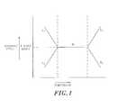
- FIG. 1is a theoretical graph showing different possible reaction regimes for different process recipes in different temperature ranges.
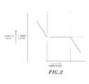
- FIGS. 2-4show different possible growth rate curves as a function of temperature for different specific chemistries.
- FIG. 5is a schematic cross section of an atomic layer deposition reactor, constructed according to a first embodiment of the invention.
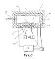
- FIG. 6is a schematic cross section of an atomic layer deposition reactor, constructed according to a second embodiment of the invention, wherein the walls are provided with a fluid recirculating system.
- FIG. 7is a schematic cross section of an atomic layer deposition reactor, constructed according to a third embodiment of the invention, wherein the substrate support is provided with a fluid recirculating system.
- FIG. 8is a schematic cross section of an atomic layer deposition reactor, constructed according to a fourth embodiment of the invention, wherein both the walls and the substrate support are provided with fluid recirculating systems.
- atomic layer depositionALD
- a suitable combination of at least two reactantsis preferably available. Even when such a suitable combination of two reactants has been selected, true self-limited atomic layer deposition will only occur in a certain temperature window.
- FIG. 1the growth of the film per cycle is given as a function of temperature.
- Wdenotes the window in which atomic layer deposition occurs.
- one monolayer of filmis deposited per full cycle. However, due to surface reconstruction or steric hindrance by large surface ligands, less than a monolayer per cycle is typically deposited.
- L 1denotes a region of increased growth per cycle at the low end of the temperature window (W), caused for certain reactants by reactant condensation.
- L 2denotes a region of decreased growth per cycle at the low end of the processing window for other reactant combinations.
- the temperature dependence described by L 2is indicative of a process with other combinations of reactants that is activation energy limited, where the reactivity of the reactants becomes too low. It should be noted that, even for chemistries exhibiting a low-temperature curve like L 2 , increased deposition will eventually occur at even lower temperatures (not shown) where condensation takes place.
- H 1indicates a situation at the high end of the temperature window where the growth per cycle increases above one monolayer. This can occur for some process recipes when the temperature is so high that thermal decomposition of one of the reactants occurs or non-volatile reaction by-products are formed.
- H 2represents a situation at the high end of the temperature window with reduced growth per cycle for other types of reactants. This may be the result of desorption or dissociation of a surface ligand that is needed to activate the surface for the next reactant. It should be noted that, even for chemistries exhibiting a high-temperature curve like H 2 , increased deposition can eventually occur at even higher temperatures (not shown) when thermal decomposition causes deposition.
- maintaining surface temperature within a certain windowis important to achieving the desired growth of a thin film on a substrate by ALD.
- the information about the growth curve for a particular reactionis typically used to select an appropriate substrate temperature.
- a substrate temperatureis chosen that falls within the window in which ALD occurs.
- the preferred embodimentstake advantage of the other information available from the growth curves to minimize deposition on the reactor walls and provide an improved ALD method and apparatus.
- the temperature of the reactor wallsis controlled independently of the substrate temperature by a separate heating or cooling system.
- the temperature of the reactor wallscan be maintained at one set point and the temperature of the substrate can be maintained at a second set point.
- Independent controldoes not mean that there is no communication between the separate heating or cooling systems.
- the ability to share information between the first and second temperature controllercan prevent undesired oscillations in temperature resulting from heat transfer from the substrate holder to the walls or vice versa.
- the walls and the substrateare both set to fall within the ALD temperature window, thereby accomplishing ALD reactions on both the substrate and the walls.
- the wall temperature and substrate temperaturedesirably set to within about 100° C. of one another, preferably within about 25° C. of one another and more preferably within about 10° C. of one another.
- the wall temperature and substrate temperaturewill generally be set to approximately the same temperature as one another. In such arrangements, at least reactant thermal decomposition, physisorption and condensation upon the walls can be controllably avoided.
- the wall temperature and substrate temperatureare arranged to have a difference in temperature that will reduce film growth upon the walls.
- the temperature of the wallswill preferably be controlled to differ from that of the substrate by greater than 10° C., in some cases greater than 20° C. or greater than 40° C. Where possible while still minimizing deposits on the walls, however, the temperature difference is minimized, since the temperature of the walls will affect the temperature of the substrate and vice versa.
- the temperature of the reaction chamber wallsis higher than the temperature of the substrate. In another embodiment the temperature of the substrate is higher than that of the reaction chamber walls.
- the walls of the reaction chamberare adjusted to a temperature that minimizes deposition (of any nature) on the walls while the substrate is adjusted to a temperature that maximizes deposition by self-limited ALD mechanisms on the substrate, depending upon the chemistry of the process recipe. In other words, the substrate temperature is maintained within the ALD window (W).
- the temperature of the reactor wallsis preferably controlled by a first temperature regulating system.
- the temperature regulating systemmaintains the reactor walls at a uniform temperature. In other arrangements, the temperature regulating system maintains different parts of the reactors walls at different temperatures.
- the first temperature regulating systemcomprises direct heaters.
- the heatersmay be resistance heaters or any other heaters known in the art.
- the first temperature regulating systemcomprises a fluid recirculating system. In the case of the fluid recirculating system, the temperature regulating system may function to heat, remove heat from or actively cool the walls of the reactor.
- the temperature of the substrateis preferably controlled by a second temperature regulating system. This is preferably accomplished by heating or cooling the substrate support.
- the substrate supportmay be a baseplate or any other substrate support known in the art. In one arrangement the entire substrate support is maintained at a uniform temperature. In other arrangements the second temperature regulating system maintains different areas of the substrate support at different temperatures. Thus it is possible to maintain different parts of the substrate at different temperatures.
- the second temperature regulating systemcomprises heaters.
- the heatersmay be resistive heaters or any heater known in the art.
- the second temperature regulating systemcomprises a fluid recirculating system.
- the temperature regulating systemmay function to heat, remove heat from or actively cool the substrate support or susceptor and thus the substrate itself.
- the temperature regulating system that controls the temperature of the substrateis preferably controllable independently from the temperature regulating system that controls the temperature of the walls, i.e., capable of being programmed with separate temperature setpoints. While the two temperature regulating systems are independently controllable, in one embodiment some data transfer between the first and second temperature controller is contemplated. For example, temperature values or PID values may be shared between the first and second temperature controller
- the temperature of the wallsis preferably set at a temperature that prevents condensation or physisorption of the reactants on the walls. This is a requirement that is foreign to conventional chemical vapor deposition where the reactants are simultaneously present in the reaction chamber. In ALD, it is essential that the reactants are sequentially and not simultaneously present in the reaction chamber. Physisorption of one reactant on the wall may disturb the ALD reaction regime, and even when this occurs only on the walls of the reactor it can be very harmful. Condensation of source chemicals on the walls can cause particle formation that can be harmful to the controlled deposition on the substrate.
- the temperature of the reactor wallsis also preferably set below the temperature at which thermal decomposition occurs.
- the actual growth rate curve for a particular reactiondepends on the combination of reactants selected.
- FIGS. 2-4some basic curves are shown.
- the growth curve shown in FIG. 2represents a situation in which growth is reduced at temperatures above the window in which ALD occurs, while growth is increased at temperatures below the window.
- the temperature of the reactor wallsis set higher than the window at which ALD occurs.
- the temperature of the reactor wallsis also preferably set below the temperature (not shown) at which the reactants thermally decompose. This will minimize unwanted deposition on the reactor walls.
- the substrateis preferably heated to a temperature that is within the window for ALD, thus allowing for the desired deposition on the substrate.
- FIG. 3represents a situation in which the properties of the reactants are such that growth is reduced at temperatures below the ALD window, while at temperatures above the window growth is increased.
- the temperature of the substratemaintained within the window for ALD while the temperature of the reactor walls is set below this.
- the temperature of the reactor wallsis preferably maintained above the temperature (not shown) at which condensation occurs, thus minimizing deposition and condensation on the reactor walls and improving the ALD deposition on the substrate.
- the substrate temperatureis preferably maintained within the ALD temperature window while the reactor wall temperature is set either higher or lower than this.
- the reactor wall temperatureis also preferably maintained above the temperature (not shown) at which condensation occurs and below the temperature (not shown) at which thermal decomposition occurs, thus minimizing accumulation of reactants and deposition on the reactor walls.
- a growth curve corresponding to FIG. 2has been obtained for the growth of ZnSe from alternating pulses of elemental Zn and Se.
- a growth of about 1 monolayer per cycleoccurs in the temperature range of 250° C. to 350° C. (Suntola, T. 1994. “Atomic Layer Epitaxy,” in Handbook of Crystal Growth 3 , Thin Films and Epitaxy, Part B: Growth Mechanisms and Dynamics, D. T. J. Hurle, Ed. Elsevier, Chapter 14, pp. 601-663).
- the temperature of the substrateis preferably set between 250° C. and 350° C. while the temperature of the reactor walls are preferably set above 350° C. (resulting in reduced growth on the walls).
- the reactor wallsare also set below the temperature at which the reactants thermally decompose. It is to be noted, however, that in this example the source chemicals are elements and in that respect they cannot thermally decompose, although Se 8 molecules may fragment into smaller selenium molecules.
- a growth curve according to FIG. 3has been reported for the atomic layer deposition of GaAs from alternating pulses of trimethylgallium and arsine.
- a growth of about 1 monolayeroccurs in the temperature range of 490° C. to 520° C. (Suntola, T. “Atomic Layer Epitaxy,” in Handbook of Crystal Growth 3, Thin Films and Epitaxy, Part B: Growth Mechanisms and Dynamics, D. T. J. Hurle, Ed. Elsevier, Chapter 14, pp. 601-663 (1994)).
- the substrate temperatureis preferably set between 490° C. and 520° C. and the temperature of the reactor walls is preferably set below 490° C. (resulting in reduced growth on the walls).
- the temperature of the reactor wallsis also preferably maintained above the temperature at which condensation of the reactants would occur.
- a growth curve according to FIG. 4has been reported for the ALD growth of SnO 2 from alternating pulses of vaporized SnCl 4 and H 2 O (Viirola and Niinistö, Thin Solid Films, 249:144-149 (1994)).
- the ALD growth ratewas maximal at a substrate temperature of about 500° C.
- the substrate temperaturewas decreased from 500° C. to 300° C.
- the growth rate of SnO 2dropped from 0.30 ⁇ /cycle to about 0.12 ⁇ /cycle.
- the wall temperatureis set at a lower level than the substrate temperature.
- the reaction chamber wall temperatureis also preferably high enough to avoid the condensation of source chemicals on the walls, which can produce particles that are harmful for thin film processes.
- the maximum possible vapor pressure of the source chemical in a chamberdepends on the coldest spot in the chamber. For example, at 92° C. the maximum vapor pressure of SnCl 4 is 400 Torr while that of water is 567 Torr.
- the reaction byproduct HClis a gas at room temperature. Consequently, with a cold spot of 92° C. the maximum possible vapor pressure of the source chemicals in the chamber is much higher than the normal operating pressure of the ALD reaction chamber, where the operating pressure is approximately in the range of 1-50 Torr. Thus, purging the surplus source chemical away from the reaction chamber should be relatively easy.
- the vapor pressure of the SnCl 4 and H 2 O source chemicals and the HCl by-productare taken into account and the reaction chamber wall temperature is preferably set well below the substrate temperature without the problem of condensation of the chemicals on the reaction chamber walls. Removal of surplus source chemicals is preferably carried out by purging with an inert gas or by pumping.
- the removal of physisorbed wateris preferably completed before any other source chemicals are introduced into the reaction chamber.
- the failure to remove physisorbed source chemicals from the reaction chamber wallsmay result in rapid uncontrolled growth of solid material on the walls and formation of solid particles that contaminate the substrate surface.
- the reaction chamber wall temperature at which physisorbed water on the walls can effectively be prevented and/or be removed during the purge period that follows the water pulseis desirably greater than about 200° C.
- the substrate temperatureis preferably set at about 500° C. while the reactor wall temperature is preferably set between about 200° C. and about 500° C., more preferably about 300° C.
- the deposition rate of MgO from Mg(thd) 2 and ozone on silicon and soda lime glass substratesshows a growth rate curve corresponding to FIG. 4.
- a maximum deposition rate of 0.27 ⁇ /cycle at 225° C.-250° C.was observed. At 170° C. the growth rate was practically zero and at 270° C. the growth rate was about 0.08 ⁇ /cycle (M. Putkonen, L.-S. Johansson, E. Rauhala and L. Niinistö, J. Mater. Chem., Vol. 9, pp. 2249-2252 (1999)).
- the reaction chamber wallsare preferably kept cooler than the susceptor or substrate support.
- the temperature of the reaction chamber wallsis preferably lowered to less than about 200° C., more preferably between about 170° C. and about 180° C.
- the substrateis preferably heated to a temperature of between about 200° C. and about 270° C., more preferably between about 225° C. and about 250° C. These temperatures will keep the walls essentially clean while the MgO thin film grows with a good ALD growth rate on the substrate.
- the temperature of the reaction chamber wallsis increased above that of the substrate.
- the reaction chamber wall temperatureis preferably increased to at least about 270° C., thus decreasing the growth rate of MgO on the walls by about 70%.
- the substrateis preferably heated to a temperature of between about 200° C. and about 270° C., more preferably between about 225° C. and about 250° C., ensuring that the ALD growth rate of MgO on the substrate will stay at the maximum level of 0.27 ⁇ /cycle.
- the walls of the reaction chamberwill need to be cleaned less frequently than in the case where the reaction chamber walls are kept at the same temperature as the substrate.
- the reaction chamber wall temperatureis preferably not set below about 170° C. because condensation of Mg(thd) 2 on the walls could occur.
- the maximum reaction chamber wall temperatureis preferably not so high that the source chemical, in this example Mg(thd) 2 , thermally decomposes on the reaction chamber walls.
- the upper limit for Mg(thd) 2is at about 400° C.-450° C.
- the substrateis preferably heated to a temperature of between about 225° C. and about 250° C.
- the wallsare preferably heated to 170° C.-200° C. or 270° C.-400° C.
- the deposition rate of CaS by ALDwas shown to be strongly dependent on the temperature when Ca(thd) 2 and H 2 S were used as source chemicals (J. Rautanen, M. Leskelä, L. Niinistö, E. Nykanen, P. Soininen, M. Uttriainen, Applied Surface Science, 82/83:553-558 (1994)).
- the deposition rate of CaS on the substrate surfacechanged from 0.12 ⁇ /cycle at 200° C. to a maximum value of 0.52 ⁇ /cycle at 350° C., possibly because the available activation energy affected the reactions.
- the substrateis preferably maintained at a temperature of 350° C.
- the reaction chamber wallsare preferably kept at a temperature above 190° C. when Ca(thd) 2 is used as a source chemical, because a suitable source temperature of Ca(thd) 2 is 190° C. and condensation of Ca(thd) 2 on the reaction chamber walls is possible below this temperature. More preferably the reaction chamber wall temperature is maintained between about 200° C. and about 290° C. to minimize the accumulation of solid material on the reaction chamber walls.
- the wallsare preferably maintained at a temperature higher than the substrate, thus reducing deposition on the walls.
- the reaction chamber wallsare preferably kept below 450° C., because thermal decomposition of Ca(thd) 2 appears to occur at temperatures of 450° C. and above.
- ALD processesmay use metal halides and ammonia as source chemicals for the deposition of metal nitride thin films, particularly in fabricating integrated circuits.
- By-productsinclude hydrogen halides.
- the hydrogen halidesmay form ammonium halides that desorb quite slowly from surfaces.
- Enhanced desorption of ammonium halides from the reaction chamber wallsis achieved in another embodiment of the present invention.
- the substrate temperatureis preferably kept at 400° C. or lower because of heat-sensitive layers or components on the substrate, the reaction chamber walls are preferably heated to temperatures above 400° C. to enhance the desorption of adsorbed reaction byproducts from the reaction chamber walls.
- the fluid recirculating systempreferably comprises a heat removal medium that is circulating through channels within the susceptor that is holding the substrate.
- Ta 2 O 5tantalum pentoxide
- H 2 Oalum pentoxide
- the deposition temperature of Ta 2 O 5is limited to about 300° C. and lower because at higher temperatures the TaCl 5 source chemical starts to etch deposited Ta 2 O 5 away and form volatile TaOCl 3 .
- This type of etchingis described in K. Kukli, M. Ritala, R. Matero, M. Leskelä, “Influence of atomic layer deposition parameters on the phase content of Ta2O 5 films,” Journal of Crystal Growth, 212:459-468 (2000).
- the deposition of Ta 2 O 5 from tantalum halide and wateris prevented on the reaction chamber walls by keeping the wall temperature above 300° C. while the substrate temperature is kept below 300° C.
- Ta 2 O 5grows by ALD on the substrate surface but the reaction chamber walls stay essentially clean.
- the temperature of the walls of the reaction chamberis also controlled to prevent harmful phenomena like condensation or decomposition from occurring on the walls.
- the wall temperatureis set at the same temperature as the substrate so that on both substrate surface and the reaction chamber wall an atomic layer deposition growth regime is realized, which will at least avoid condensation and thermal decomposition.
- the wall temperatureis preferably set at a higher value than the substrate temperature to prevent deposition on the wall.
- the wall temperaturepreferably remains below the value where thermal decomposition of a reactant can occur.
- the wall temperaturecan be selected to be higher than the substrate temperature but lower than the thermal decomposition limit, while in other arrangements the wall temperature is set lower than the substrate temperature but higher than the condensation limit.
- an apparatus for atomic layer depositioncomprises a first heater, a first temperature sensor and a first temperature controller to heat the substrate and control the substrate temperature.
- an atomic layer deposition reactoradditionally comprises a second temperature regulating system, such as a second heater, a second temperature sensor and a second temperature controller, to heat the walls of the reaction chamber and control the temperature of the walls of the reaction chamber.
- a second temperature regulating systemsuch as a second heater, a second temperature sensor and a second temperature controller
- the first and second temperature control systemscomprise resistance heaters.
- reference numeral 1indicates reaction chamber walls.
- a substrate support structure 2supports a substrate 7 .
- the support structure 2is movable relative to the walls 1 , facilitating loading and unloading substrates in an automated fashion.
- the support structurecan comprise a base plate configured to lower for access by a wafer handling robot, and to rise into sealing contact with the chamber walls 1 .
- the substrate support structure 2is provided with a first heater 3 and a first temperature sensor 4 to sense the temperature of the substrate support structure 2 .
- the first temperature sensor 4is connected to a first temperature controller 8 , which provides an input signal to a first power supply 9 to control the power applied to the first heater 3 , which is also connected to the first power supply 9 .
- a second heater 5heats the reaction chamber walls 1 and the temperature of the walls 1 is sensed by a second temperature sensor 6 , which is connected to a second temperature controller 10 .
- the second temperature controller 10provides an input signal for a second power supply 11 , connected to the second heater 5 , to control the power applied to the second heater 5 .
- the dashed line between the first temperature controller 8 and the second temperature controller 10represents a possible data transfer line. The data transfer line may be used to share temperature and PID information between the controllers, thus preventing oscillation of the temperature of the substrate support 2 and reaction chamber walls 1 .
- a plurality of temperature sensorscan be connected to each controller and that control can be split into zones, particularly within the walls.
- a plurality of heaterscan be controlled by each controller and each zone may hold a separate heater.
- the temperature sensorscan each provide an input to the temperature controller and different parts of the walls can be maintained at different temperatures.
- more than one temperature sensor and more than one heaterare present in the substrate support, allowing for different parts of the substrate to be maintained at different temperatures.
- powercan be applied to a plurality of heaters and it is possible to adjust the power level for each heater.
- the preferred chamberis located within a separate vacuum vessel.
- the vacuum vesselis not exposed to reactants, and so temperature control of the vacuum vessel walls is not critical.
- parts of the vacuum vessel wallscan be exposed to the vapor phase reactants during processing.
- those exposed parts of the vacuum vessel wallseffectively form part of the reaction chamber walls, and are preferably also maintained at a temperature that minimizes deposition.
- unexposed portions of the chamber wallsneed not have their temperature separately controlled.
- One reactant infeed line 20is shown in schematic FIG. 5 . However, for each reactant used in the process a separate reactant infeed line is preferably present.
- the gasesare exhausted through an outlet channel 30 , which is connected with a vacuum pump (not shown).
- a vacuum pumpnot shown.
- Different temperatures for substrate and reaction chamber wallscan be achieved because both the walls and the substrate support structure are inflicted with thermal losses to the environment.
- the illustrated heaters 3 , 5are embedded within the substrate support 2 and chamber walls 1 , respectively.
- the heaterscan also comprise independently controlled heating plates adjacent to the support and adjacent to the walls.
- two or more heating systemscan be radiative or inductive, such that they can remotely heat the support and walls, respectively, with independent control.
- either the reaction chamber walls, or the substrate support structure, or bothcan be provided with channels connected to a fluid recirculating system, as discussed below with respect to the further embodiments of the invention.
- the corresponding heateris a fluid heater, heating the fluid in the recirculating system.
- a fluid recirculating systemprovides not only the possibility of heating a substrate support or reactor wall, but also allows the removal of heat from the object through which the fluid is circulating. If in the case of a heat removal requirement the natural heat loss of the recirculating system is not sufficient to maintain a controlled temperature, the recirculating system can be equipped with an active cooling element instead of or in addition to the heater. This is particularly relevant to the case where the substrate temperature is controlled at a lower value than the temperature of the walls and heat is to be removed from the substrate support in order to maintain the desired substrate temperature.
- the choice of the circulating fluiddepends on the maximum allowed fluid temperature and the intended application, as will be recognized by one skilled in the art. Several possible choices are described below, but any heat transfer fluid known in the art may be used.
- DOWTHERM ATMis a eutectic mixture of diphenyl oxide and biphenyl oxide that has excellent thermal stability at 400° C.
- SYLTHERM 800TMis a non-corrosive silicone fluid that can operate more than 10 years at 400° C. without fouling the heating system.
- the heat capacity of DOWTHERM ATM2.7 J/g° C. and that of SYLTHERM 800TMis 2.2 J/g° C.
- Liquid metalsare another class of heat transfer materials that could be used as circulation fluid in the apparatus of the present invention.
- Mercury (Hg) and some eutectic alloys of alkali metals (Na, K, Rb, Cs)are liquids at room temperature. However, they either have high toxicity (Hg) or very high reactivity (Na, K, Rb, Cs).
- gallium metalhas low reactivity and it is not toxic. Pure gallium metal melts at 30° C. and has a very low vapor pressure (1 Torr at 1349° C.).
- Eutectic alloys of gallium and e.g., tin or indiumare liquids at room temperature and thus any clogging of the fluid circulation tubes is avoided when the reactor is cooled to room temperature.
- the heat capacity of Gais 0.37 J/g ⁇ ° C. If the reaction chamber is made of titanium metal (heat capacity 0.52 J/g ⁇ ° C.), cooling 1 g of titanium by 1° C. heats 1.4 g of Ga by 1° C.
- Liquid metalmay be circulated with, e.g., an electromagnetic pump that has no moving parts.
- gaseous fluidscan be applied.
- the volumetric heat capacity of gasesis less than that of fluids, in many practical cases where the heat transport requirement is not excessively high, the use of gaseous fluids is practical.
- the table belowprovides the heat capacity, density and volumetric heat capacity for several gaseous fluids.
- cooling 1 g of titanium by 1° C.would heat 0.4 liters of nitrogen or 0.6 liters of helium by 1° C. when the gas pressure is 1 atm.
- Maximum allowed gas pressuredepends on the design of the gas circulation system.
- FIG. 6shows an embodiment in which the reactor walls 1 are provided with a fluid recirculating system.
- Fluid circulation channels 16are formed within the walls 1 , and are connected to a fluid recirculating pump and a wall temperature regulator 15 via connection lines 17 .
- the second temperature controller 10provides an input signal to the fluid recirculating pump and the wall temperature regulator 15 to control the power applied to the fluid, such that the temperature of the walls 1 remains constant.
- the wall temperature regulator 15may also include a refrigerator unit (not shown) for cooling the recirculating fluid.
- the temperature of the walls 1is sensed by the second temperature sensor 6 , which is connected to the second temperature controller 10 .
- the dashed line between the first temperature controller 8 and the second temperature controller 10represents a possible data transfer line.
- the substrate support 2is provided with a fluid recirculating system.
- the systemincludes fluid recirculating channels 40 through the substrate support, connected to a fluid recirculating pump and a first temperature regulator 60 .
- the temperature of the fluid, and thus of the substrate support 2 and substrate 7is maintained by input from the first temperature controller 50 to the fluid recirculating pump and first temperature regulator 60 .
- the first temperature regulator 60may also include a refrigerator unit (not shown) for cooling the recirculating fluid.
- the walls 1have their temperature controlled by a system as described with respect to FIG. 5 .
- FIG. 8the walls 1 and the substrate support 2 are provided with independently controlled fluid recirculating systems.
- the ALD reactoris thus shown with the system of FIG. 6 for the wall 1 temperature control, and the system of FIG. 7 for substrate support 2 temperature control.
- the dashed line between the first temperature controller 50 and the second temperature controller 10represents a possible data transfer line.
Landscapes
- Chemical & Material Sciences (AREA)
- General Chemical & Material Sciences (AREA)
- Chemical Kinetics & Catalysis (AREA)
- Engineering & Computer Science (AREA)
- Materials Engineering (AREA)
- Mechanical Engineering (AREA)
- Metallurgy (AREA)
- Organic Chemistry (AREA)
- Inorganic Chemistry (AREA)
- Chemical Vapour Deposition (AREA)
- Physical Or Chemical Processes And Apparatus (AREA)
Abstract
Description
This application is related to U.S. application Ser. Nos. 09/769,562 filed Jan. 25, 2001, now U.S. Pat. No. 6,579,374, and 09/568,077 filed May 10, 2000, now U.S. Pat. No. 6,562,140.
This invention relates to the field of reactor design for atomic layer deposition of thin films onto substrates such as wafers and flat panel displays.
In atomic layer deposition (ALD), a substrate placed in a reaction space is subjected to alternating pulses of at least two different reactants suitable for producing a desired thin film on the substrate. When the substrate is exposed to a pulse of the first reactant, a monolayer of the first reactant is chemisorbed on the surface of the substrate until all of the available surface sites are occupied with an adsorbed portion of a reactant molecule and saturation occurs. The surface sites may be occupied by the whole of or by a fragment of a vapor-phase reactant molecule, such as when a metal chloride molecule chemisorbs on a surface site that has a hydroxyl group. For example, TaCl5may chemisorb as a TaCl4fragment, with HCl released as a gaseous byproduct. The reaction is chemically self-limiting because gaseous first reactant will not adsorb or react with the portion of the first reactant that has already been adsorbed on the substrate surface. The excess of the reactant is then removed by purging the reaction space with an inert gas and/or evacuating the reaction space.
Subsequently, the substrate is exposed to a pulse of the second reactant, which chemically reacts with the adsorbed portion of the first reactant molecules until the reaction is complete and the surface is covered with a monolayer of the chemisorbed portion of the second reactant. Fragments of the second reactant will be adsorbed under some reaction conditions. For example, when water is used as the second reactant it may leave a fragment of H2O, such as hydroxyl groups (—OH) on the surface. Similarly, when ammonia (NH3) is used as the second reactant it may leave fragments such as NH or NH2groups on the surface. Reaction conditions such as temperature and pressure are chosen to ensure that physisorption of more than one monolayer of the first or second reactant (or portions thereof) on the substrate cannot occur. In this way the growth of the film proceeds atomic layer by atomic layer.
In the art of atomic layer deposition, the temperature of the substrate is not considered to be very critical because the growth rate of the film is not dependent on the temperature of the substrate but rather on the sequential exposure to the different reactant pulses. In fact, relative temperature independence of the process is a primary advantage of ALD, leading to perfect step-wise coverage despite temperature non-uniformities across large substrates. The temperature is preferably high enough to prevent condensation of the reactants on the substrate and to allow the reaction to proceed at a sufficiently high rate. On the other hand, the substrate temperature preferably remains below the limit where thermal decomposition of the individual reactants occurs. For many combinations of reactants, such as metal halides and water, the reaction is able to proceed at temperatures as low as room temperature and as high as the thermal decomposition temperature limit for the reactants. Thus, a wide temperature window for atomic layer deposition is available.
Accordingly, the temperature of the wall of the reactor is not considered to be an important parameter for ALD. Both hot wall and cold wall designs have been used. In reactors with automated substrate transfer, cold wall designs are typically used. A cold wall reactor design is described in U.S. Pat. No. 5,879,465 to Genus Inc. The reactor described comprises a heater, adapted for heating a substrate supported on a support pedestal, and cooling lines for passing coolant through a portion of the body. This design results in a lower region of the reactor that is hot and an upper region of the reactor that is cool.
In conventional chemical vapor deposition (CVD), a cold-wall design is an advantage. In such a design, where only the substrate, placed on a substrate support, is heated, deposition on the cold wall is prevented. This reduces the required cleaning frequency of the system. However, in contrast, cold regions in the wall of an ALD reactor are particularly harmful for the process for a variety of reasons. First of all, increased adsorption or even condensation of the reactants on the cold region of the wall can occur. Physisorbed or condensed material sticks well to a wall at low temperature and thus may not be effectively removed from the reaction space during the purge between the two reactant pulses. This can result in extra consumption of material and accelerated contamination of the reactor wall. Again, this is contrary to conventional CVD where a reduced wall temperature results in reduced contamination of the wall. Furthermore, when the reaction space above the substrate is on the average at a much lower temperature than the substrate itself, more gas is required for purging the reaction space between the reactant pulses because of the increased gas density at low temperature.
Hot wall batch reactors for ALD are known in the art and they avoid the above-noted disadvantages of cold wall ALD reactors. However, heating of the substrates in hot wall batch reactors occurs indirectly and proceeds very slowly at the relatively moderate temperatures used for ALD. Additionally, the loading of substrates in these hot-wall batch reactors is difficult to automate, making them less suitable for production purposes.
It is an object of the present invention to provide a reactor for ALD, comprising automated substrate transfer into and out of the reactor, that avoids the above described disadvantages and provides an improved control of the ALD process. It is a further object of the invention to provide a method for atomic layer deposition in which harmful reactions on the reaction chamber walls are prevented. It is another object of the invention to provide a method for atomic layer deposition that provides a lower deposition rate on the walls of the reaction chamber than on the substrate, while avoiding harmful reactions on the walls that disturb ALD growth on the substrate.
In accordance with one aspect of the invention, an atomic layer deposition reactor, comprising a heater, temperature sensor and a temperature controller to heat the substrate and control the substrate temperature, is provided with an additional heater, temperature sensor and temperature controller to heat the walls of the reaction chamber and control the temperature of the reaction chamber walls independently from the temperature of the substrate.
In accordance with another aspect of the invention, a method is provided for atomic layer deposition of a film onto a substrate in a reaction chamber. The method includes controlling the temperature of the substrate and additionally controlling the temperature of the walls of the reaction chamber at a level close enough to the substrate temperature to prevent harmful, non-ALD reactions at the reaction chamber walls. Furthermore, the temperature of the walls can be controlled at a level higher or lower than the substrate temperature. The difference between the substrate temperature and the wall temperature is preferably selected, depending upon the chemistry of the process, to result in a deposition rate on the walls that is lower than on the substrate, while avoiding harmful reactions on the walls.
In order to realize atomic layer deposition (ALD), a suitable combination of at least two reactants is preferably available. Even when such a suitable combination of two reactants has been selected, true self-limited atomic layer deposition will only occur in a certain temperature window. InFIG. 1 , the growth of the film per cycle is given as a function of temperature. In this figure, W denotes the window in which atomic layer deposition occurs. In the ideal case, represented in the drawings, one monolayer of film is deposited per full cycle. However, due to surface reconstruction or steric hindrance by large surface ligands, less than a monolayer per cycle is typically deposited. L1 denotes a region of increased growth per cycle at the low end of the temperature window (W), caused for certain reactants by reactant condensation. L2 denotes a region of decreased growth per cycle at the low end of the processing window for other reactant combinations. The temperature dependence described by L2 is indicative of a process with other combinations of reactants that is activation energy limited, where the reactivity of the reactants becomes too low. It should be noted that, even for chemistries exhibiting a low-temperature curve like L2, increased deposition will eventually occur at even lower temperatures (not shown) where condensation takes place.
H1 indicates a situation at the high end of the temperature window where the growth per cycle increases above one monolayer. This can occur for some process recipes when the temperature is so high that thermal decomposition of one of the reactants occurs or non-volatile reaction by-products are formed. H2 represents a situation at the high end of the temperature window with reduced growth per cycle for other types of reactants. This may be the result of desorption or dissociation of a surface ligand that is needed to activate the surface for the next reactant. It should be noted that, even for chemistries exhibiting a high-temperature curve like H2, increased deposition can eventually occur at even higher temperatures (not shown) when thermal decomposition causes deposition.
As is made clear inFIG. 1 , maintaining surface temperature within a certain window, albeit a wide window, is important to achieving the desired growth of a thin film on a substrate by ALD. Conventionally, the information about the growth curve for a particular reaction is typically used to select an appropriate substrate temperature. Thus, a substrate temperature is chosen that falls within the window in which ALD occurs. The preferred embodiments take advantage of the other information available from the growth curves to minimize deposition on the reactor walls and provide an improved ALD method and apparatus.
In the preferred embodiments, the temperature of the reactor walls is controlled independently of the substrate temperature by a separate heating or cooling system. Thus the temperature of the reactor walls can be maintained at one set point and the temperature of the substrate can be maintained at a second set point. Independent control does not mean that there is no communication between the separate heating or cooling systems. Thus while being independently controllable, it is possible in some arrangements to share information concerning temperature values or PID values between a first and second temperature controller. For example, if the operation of the temperature controllers is based on PID values, with a parameter for the present temperature value, the temperature history (integration) and the future temperature (derivation), the ability to share information between the first and second temperature controller can prevent undesired oscillations in temperature resulting from heat transfer from the substrate holder to the walls or vice versa.
In some arrangements, the walls and the substrate are both set to fall within the ALD temperature window, thereby accomplishing ALD reactions on both the substrate and the walls. In this case, the wall temperature and substrate temperature desirably set to within about 100° C. of one another, preferably within about 25° C. of one another and more preferably within about 10° C. of one another. The wall temperature and substrate temperature will generally be set to approximately the same temperature as one another. In such arrangements, at least reactant thermal decomposition, physisorption and condensation upon the walls can be controllably avoided.
In other arrangements, the wall temperature and substrate temperature are arranged to have a difference in temperature that will reduce film growth upon the walls. In such a case, the temperature of the walls will preferably be controlled to differ from that of the substrate by greater than 10° C., in some cases greater than 20° C. or greater than 40° C. Where possible while still minimizing deposits on the walls, however, the temperature difference is minimized, since the temperature of the walls will affect the temperature of the substrate and vice versa.
In one embodiment the temperature of the reaction chamber walls is higher than the temperature of the substrate. In another embodiment the temperature of the substrate is higher than that of the reaction chamber walls. Thus the walls of the reaction chamber are adjusted to a temperature that minimizes deposition (of any nature) on the walls while the substrate is adjusted to a temperature that maximizes deposition by self-limited ALD mechanisms on the substrate, depending upon the chemistry of the process recipe. In other words, the substrate temperature is maintained within the ALD window (W).
The temperature of the reactor walls is preferably controlled by a first temperature regulating system. In one arrangement, the temperature regulating system maintains the reactor walls at a uniform temperature. In other arrangements, the temperature regulating system maintains different parts of the reactors walls at different temperatures.
Further, in one embodiment, the first temperature regulating system comprises direct heaters. The heaters may be resistance heaters or any other heaters known in the art. In another embodiment the first temperature regulating system comprises a fluid recirculating system. In the case of the fluid recirculating system, the temperature regulating system may function to heat, remove heat from or actively cool the walls of the reactor.
The temperature of the substrate is preferably controlled by a second temperature regulating system. This is preferably accomplished by heating or cooling the substrate support. The substrate support may be a baseplate or any other substrate support known in the art. In one arrangement the entire substrate support is maintained at a uniform temperature. In other arrangements the second temperature regulating system maintains different areas of the substrate support at different temperatures. Thus it is possible to maintain different parts of the substrate at different temperatures.
Further, in one embodiment the second temperature regulating system comprises heaters. The heaters may be resistive heaters or any heater known in the art. In another embodiment the second temperature regulating system comprises a fluid recirculating system. In the case of the fluid recirculating system, the temperature regulating system may function to heat, remove heat from or actively cool the substrate support or susceptor and thus the substrate itself. The temperature regulating system that controls the temperature of the substrate is preferably controllable independently from the temperature regulating system that controls the temperature of the walls, i.e., capable of being programmed with separate temperature setpoints. While the two temperature regulating systems are independently controllable, in one embodiment some data transfer between the first and second temperature controller is contemplated. For example, temperature values or PID values may be shared between the first and second temperature controller
In order to minimize deposition on the walls, the temperature of the walls is preferably set at a temperature that prevents condensation or physisorption of the reactants on the walls. This is a requirement that is foreign to conventional chemical vapor deposition where the reactants are simultaneously present in the reaction chamber. In ALD, it is essential that the reactants are sequentially and not simultaneously present in the reaction chamber. Physisorption of one reactant on the wall may disturb the ALD reaction regime, and even when this occurs only on the walls of the reactor it can be very harmful. Condensation of source chemicals on the walls can cause particle formation that can be harmful to the controlled deposition on the substrate. The temperature of the reactor walls is also preferably set below the temperature at which thermal decomposition occurs.
The actual growth rate curve for a particular reaction depends on the combination of reactants selected. InFIGS. 2-4 some basic curves are shown. For example, the growth curve shown inFIG. 2 represents a situation in which growth is reduced at temperatures above the window in which ALD occurs, while growth is increased at temperatures below the window. Thus, in the case of reactants that have a growth curve as shown inFIG. 2 , it is preferred to have the temperature of the reactor walls set higher than the window at which ALD occurs. However the temperature of the reactor walls is also preferably set below the temperature (not shown) at which the reactants thermally decompose. This will minimize unwanted deposition on the reactor walls. At the same time, the substrate is preferably heated to a temperature that is within the window for ALD, thus allowing for the desired deposition on the substrate.
It is also possible that deposition or growth is reduced at temperatures both above and below the ALD temperature window. This situation is depicted in FIG.4. In such a situation, the substrate temperature is preferably maintained within the ALD temperature window while the reactor wall temperature is set either higher or lower than this. The reactor wall temperature is also preferably maintained above the temperature (not shown) at which condensation occurs and below the temperature (not shown) at which thermal decomposition occurs, thus minimizing accumulation of reactants and deposition on the reactor walls.
One skilled in the art will be able to identify the type of growth curve that is representative of a particular reaction. Several examples of reactions corresponding to the curves shown inFIGS. 2-4 are described below.
A growth curve corresponding toFIG. 2 has been obtained for the growth of ZnSe from alternating pulses of elemental Zn and Se. A growth of about 1 monolayer per cycle occurs in the temperature range of 250° C. to 350° C. (Suntola, T. 1994. “Atomic Layer Epitaxy,” in Handbook ofCrystal Growth 3, Thin Films and Epitaxy, Part B: Growth Mechanisms and Dynamics, D. T. J. Hurle, Ed. Elsevier, Chapter 14, pp. 601-663). Thus, the temperature of the substrate is preferably set between 250° C. and 350° C. while the temperature of the reactor walls are preferably set above 350° C. (resulting in reduced growth on the walls). In general, the reactor walls are also set below the temperature at which the reactants thermally decompose. It is to be noted, however, that in this example the source chemicals are elements and in that respect they cannot thermally decompose, although Se8molecules may fragment into smaller selenium molecules.
A growth curve according toFIG. 3 has been reported for the atomic layer deposition of GaAs from alternating pulses of trimethylgallium and arsine. A growth of about 1 monolayer occurs in the temperature range of 490° C. to 520° C. (Suntola, T. “Atomic Layer Epitaxy,” in Handbook ofCrystal Growth 3, Thin Films and Epitaxy, Part B: Growth Mechanisms and Dynamics, D. T. J. Hurle, Ed. Elsevier, Chapter 14, pp. 601-663 (1994)).
In this situation, the substrate temperature is preferably set between 490° C. and 520° C. and the temperature of the reactor walls is preferably set below 490° C. (resulting in reduced growth on the walls). However, the temperature of the reactor walls is also preferably maintained above the temperature at which condensation of the reactants would occur.
A growth curve according toFIG. 4 has been reported for the ALD growth of SnO2from alternating pulses of vaporized SnCl4and H2O (Viirola and Niinistö, Thin Solid Films, 249:144-149 (1994)). The ALD growth rate was maximal at a substrate temperature of about 500° C. When the substrate temperature was decreased from 500° C. to 300° C., the growth rate of SnO2dropped from 0.30 Å/cycle to about 0.12 Å/cycle.
In this case, where the ALD reaction is considered thermally driven, in the sense that ALD reactions are facilitated at higher temperatures and inhibited at lower temperatures, it is preferable to set the wall temperature at a lower level than the substrate temperature. The reaction chamber wall temperature is also preferably high enough to avoid the condensation of source chemicals on the walls, which can produce particles that are harmful for thin film processes. The maximum possible vapor pressure of the source chemical in a chamber depends on the coldest spot in the chamber. For example, at 92° C. the maximum vapor pressure of SnCl4is 400 Torr while that of water is 567 Torr. The reaction byproduct HCl is a gas at room temperature. Consequently, with a cold spot of 92° C. the maximum possible vapor pressure of the source chemicals in the chamber is much higher than the normal operating pressure of the ALD reaction chamber, where the operating pressure is approximately in the range of 1-50 Torr. Thus, purging the surplus source chemical away from the reaction chamber should be relatively easy.
In one embodiment of the present invention, the vapor pressure of the SnCl4and H2O source chemicals and the HCl by-product are taken into account and the reaction chamber wall temperature is preferably set well below the substrate temperature without the problem of condensation of the chemicals on the reaction chamber walls. Removal of surplus source chemicals is preferably carried out by purging with an inert gas or by pumping.
It is also important to take into account the adsorption of water. Water adsorbs easily on surfaces at low temperatures, due to the polarity of the water molecule. At room temperature there can be 10-100 molecular layers of H2O on surfaces, possibly because of hydrogen bonds between the water molecules. The removal of physisorbed water is preferably completed before any other source chemicals are introduced into the reaction chamber. The failure to remove physisorbed source chemicals from the reaction chamber walls may result in rapid uncontrolled growth of solid material on the walls and formation of solid particles that contaminate the substrate surface. The reaction chamber wall temperature at which physisorbed water on the walls can effectively be prevented and/or be removed during the purge period that follows the water pulse is desirably greater than about 200° C.
As a result of the reaction conditions described above, in the case of ALD deposition of SnO2from vaporized SnCl4and H2O the substrate temperature is preferably set at about 500° C. while the reactor wall temperature is preferably set between about 200° C. and about 500° C., more preferably about 300° C.
The deposition rate of MgO from Mg(thd)2and ozone on silicon and soda lime glass substrates shows a growth rate curve corresponding toFIG. 4. A maximum deposition rate of 0.27 Å/cycle at 225° C.-250° C. was observed. At 170° C. the growth rate was practically zero and at 270° C. the growth rate was about 0.08 Å/cycle (M. Putkonen, L.-S. Johansson, E. Rauhala and L. Niinistö, J. Mater. Chem., Vol. 9, pp. 2249-2252 (1999)).
According to one embodiment of the present invention, the reaction chamber walls are preferably kept cooler than the susceptor or substrate support. In the case of MgO deposition, the temperature of the reaction chamber walls is preferably lowered to less than about 200° C., more preferably between about 170° C. and about 180° C. The substrate is preferably heated to a temperature of between about 200° C. and about 270° C., more preferably between about 225° C. and about 250° C. These temperatures will keep the walls essentially clean while the MgO thin film grows with a good ALD growth rate on the substrate.
According to another embodiment of the present invention the temperature of the reaction chamber walls is increased above that of the substrate. The reaction chamber wall temperature is preferably increased to at least about 270° C., thus decreasing the growth rate of MgO on the walls by about 70%. The substrate is preferably heated to a temperature of between about 200° C. and about 270° C., more preferably between about 225° C. and about 250° C., ensuring that the ALD growth rate of MgO on the substrate will stay at the maximum level of 0.27 Å/cycle.
In both of these embodiments the walls of the reaction chamber will need to be cleaned less frequently than in the case where the reaction chamber walls are kept at the same temperature as the substrate. When using Mg(thd)2the reaction chamber wall temperature is preferably not set below about 170° C. because condensation of Mg(thd)2on the walls could occur. On the other hand, the maximum reaction chamber wall temperature is preferably not so high that the source chemical, in this example Mg(thd)2, thermally decomposes on the reaction chamber walls. The upper limit for Mg(thd)2is at about 400° C.-450° C. In summary, while the substrate is preferably heated to a temperature of between about 225° C. and about 250° C., the walls are preferably heated to 170° C.-200° C. or 270° C.-400° C.
The deposition rate of CaS by ALD was shown to be strongly dependent on the temperature when Ca(thd)2and H2S were used as source chemicals (J. Rautanen, M. Leskelä, L. Niinistö, E. Nykanen, P. Soininen, M. Uttriainen, Applied Surface Science, 82/83:553-558 (1994)). The deposition rate of CaS on the substrate surface changed from 0.12 Å/cycle at 200° C. to a maximum value of 0.52 Å/cycle at 350° C., possibly because the available activation energy affected the reactions. According to one embodiment of the present invention, the substrate is preferably maintained at a temperature of 350° C. while the walls are preferably maintained at a lower temperature to reduce the deposition rate on the walls. However, the reaction chamber walls are preferably kept at a temperature above 190° C. when Ca(thd)2is used as a source chemical, because a suitable source temperature of Ca(thd)2is 190° C. and condensation of Ca(thd)2on the reaction chamber walls is possible below this temperature. More preferably the reaction chamber wall temperature is maintained between about 200° C. and about 290° C. to minimize the accumulation of solid material on the reaction chamber walls.
This process also follows the curve of FIG.4. Thus, in another embodiment the walls are preferably maintained at a temperature higher than the substrate, thus reducing deposition on the walls. However, the reaction chamber walls are preferably kept below 450° C., because thermal decomposition of Ca(thd)2appears to occur at temperatures of 450° C. and above.
ALD processes may use metal halides and ammonia as source chemicals for the deposition of metal nitride thin films, particularly in fabricating integrated circuits. By-products include hydrogen halides. The hydrogen halides may form ammonium halides that desorb quite slowly from surfaces. Enhanced desorption of ammonium halides from the reaction chamber walls is achieved in another embodiment of the present invention. Although the substrate temperature is preferably kept at 400° C. or lower because of heat-sensitive layers or components on the substrate, the reaction chamber walls are preferably heated to temperatures above 400° C. to enhance the desorption of adsorbed reaction byproducts from the reaction chamber walls. In this embodiment it may be necessary to remove heat from the substrate so that heat from the walls does not cause the substrate to exceed any temperature limit imposed by substrate materials, e.g., 400° C. for high-k materials that will be used in integrated circuits. Thermal energy is preferably actively removed from the substrate by the use of the fluid recirculating system, as described with respect toFIGS. 7 and 8 . The fluid recirculating system preferably comprises a heat removal medium that is circulating through channels within the susceptor that is holding the substrate.
Another exemplary ALD recipe to which the principles and advantages described herein can be applied is the deposition of tantalum pentoxide (Ta2O5) from TaCl5and H2O. Usually the deposition temperature of Ta2O5is limited to about 300° C. and lower because at higher temperatures the TaCl5source chemical starts to etch deposited Ta2O5away and form volatile TaOCl3. This type of etching is described in K. Kukli, M. Ritala, R. Matero, M. Leskelä, “Influence of atomic layer deposition parameters on the phase content of Ta2O5films,” Journal of Crystal Growth, 212:459-468 (2000). According to one embodiment of the present invention, the deposition of Ta2O5from tantalum halide and water is prevented on the reaction chamber walls by keeping the wall temperature above 300° C. while the substrate temperature is kept below 300° C. Ta2O5grows by ALD on the substrate surface but the reaction chamber walls stay essentially clean. As described with respect to Example 5, depending up on the reactor configuration, it may be advisable to provide plumbing capable of removing heat from the substrate support, such as illustrate inFIGS. 7 and 8 , to maintain the substrate temperature below 300° C.
These examples further demonstrate that temperature control can be important to the ALD process. Controlling the temperature of the substrate within certain limits is a prerequisite to achieving a desired result. However, as disclosed herein, the temperature of the walls of the reaction chamber is also controlled to prevent harmful phenomena like condensation or decomposition from occurring on the walls. In the simplest embodiment, the wall temperature is set at the same temperature as the substrate so that on both substrate surface and the reaction chamber wall an atomic layer deposition growth regime is realized, which will at least avoid condensation and thermal decomposition. However, in the situation of a growth curve as inFIG. 2 the wall temperature is preferably set at a higher value than the substrate temperature to prevent deposition on the wall. At the same time, the wall temperature preferably remains below the value where thermal decomposition of a reactant can occur. On the other hand, in the case of a growth curve as inFIG. 3 it is preferable to control the wall temperature at a lower value than the temperature of the substrate for the same reason of preventing or reducing the deposition onto the wall. In this case the temperature is preferably not so low that condensation of a reactant on the wall occurs. Finally, in the case of a growth curve as inFIG. 4 , the wall temperature can be selected to be higher than the substrate temperature but lower than the thermal decomposition limit, while in other arrangements the wall temperature is set lower than the substrate temperature but higher than the condensation limit.
In the art, an apparatus for atomic layer deposition comprises a first heater, a first temperature sensor and a first temperature controller to heat the substrate and control the substrate temperature. In the apparatus according to the preferred embodiments, an atomic layer deposition reactor additionally comprises a second temperature regulating system, such as a second heater, a second temperature sensor and a second temperature controller, to heat the walls of the reaction chamber and control the temperature of the walls of the reaction chamber. It will be understood from the descriptions of the preferred embodiments below that the temperature regulating systems need not always be heaters, although one of the two temperature regulators will generally be a heater.
In a first embodiment, represented inFIG. 5 , the first and second temperature control systems comprise resistance heaters. InFIG. 5 ,reference numeral 1 indicates reaction chamber walls. Asubstrate support structure 2 supports a substrate7. Advantageously, thesupport structure 2 is movable relative to thewalls 1, facilitating loading and unloading substrates in an automated fashion. For example, the support structure can comprise a base plate configured to lower for access by a wafer handling robot, and to rise into sealing contact with thechamber walls 1.
Thesubstrate support structure 2 is provided with afirst heater 3 and a first temperature sensor4 to sense the temperature of thesubstrate support structure 2. The first temperature sensor4 is connected to afirst temperature controller 8, which provides an input signal to afirst power supply 9 to control the power applied to thefirst heater 3, which is also connected to thefirst power supply 9. Asecond heater 5 heats thereaction chamber walls 1 and the temperature of thewalls 1 is sensed by asecond temperature sensor 6, which is connected to asecond temperature controller 10. Thesecond temperature controller 10 provides an input signal for asecond power supply 11, connected to thesecond heater 5, to control the power applied to thesecond heater 5. The dashed line between thefirst temperature controller 8 and thesecond temperature controller 10 represents a possible data transfer line. The data transfer line may be used to share temperature and PID information between the controllers, thus preventing oscillation of the temperature of thesubstrate support 2 andreaction chamber walls 1.
It will be understood by the skilled artisan that a plurality of temperature sensors can be connected to each controller and that control can be split into zones, particularly within the walls. In addition, a plurality of heaters can be controlled by each controller and each zone may hold a separate heater. Thus, the temperature sensors can each provide an input to the temperature controller and different parts of the walls can be maintained at different temperatures. Similarly, in another embodiment more than one temperature sensor and more than one heater are present in the substrate support, allowing for different parts of the substrate to be maintained at different temperatures. In this case power can be applied to a plurality of heaters and it is possible to adjust the power level for each heater. An analogous system for zoned control of substrate temperature (for a radiantly heated substrate) is disclosed, for example, in U.S. Pat. No. 4,836,138 to Robinson et al., issued Jun. 6, 1989.
Additionally, the preferred chamber is located within a separate vacuum vessel. In the preferred embodiments, the vacuum vessel is not exposed to reactants, and so temperature control of the vacuum vessel walls is not critical. In some arrangements, however, parts of the vacuum vessel walls can be exposed to the vapor phase reactants during processing. In such arrangements, those exposed parts of the vacuum vessel walls effectively form part of the reaction chamber walls, and are preferably also maintained at a temperature that minimizes deposition. Where not all of the chamber walls are exposed to reactants, on the other hand, unexposed portions of the chamber walls need not have their temperature separately controlled.
Onereactant infeed line 20 is shown in schematic FIG.5. However, for each reactant used in the process a separate reactant infeed line is preferably present. The gases are exhausted through anoutlet channel 30, which is connected with a vacuum pump (not shown). Different temperatures for substrate and reaction chamber walls can be achieved because both the walls and the substrate support structure are inflicted with thermal losses to the environment.
The illustratedheaters substrate support 2 andchamber walls 1, respectively. However, the skilled artisan will appreciate that the heaters can also comprise independently controlled heating plates adjacent to the support and adjacent to the walls. In still other arrangements, two or more heating systems can be radiative or inductive, such that they can remotely heat the support and walls, respectively, with independent control.
As an alternative, either the reaction chamber walls, or the substrate support structure, or both, can be provided with channels connected to a fluid recirculating system, as discussed below with respect to the further embodiments of the invention. In such arrangements, the corresponding heater is a fluid heater, heating the fluid in the recirculating system. With fluid heating systems, temperatures up to 400° C. can easily be achieved. A fluid recirculating system provides not only the possibility of heating a substrate support or reactor wall, but also allows the removal of heat from the object through which the fluid is circulating. If in the case of a heat removal requirement the natural heat loss of the recirculating system is not sufficient to maintain a controlled temperature, the recirculating system can be equipped with an active cooling element instead of or in addition to the heater. This is particularly relevant to the case where the substrate temperature is controlled at a lower value than the temperature of the walls and heat is to be removed from the substrate support in order to maintain the desired substrate temperature.
The choice of the circulating fluid depends on the maximum allowed fluid temperature and the intended application, as will be recognized by one skilled in the art. Several possible choices are described below, but any heat transfer fluid known in the art may be used.
Dow Chemical manufactures organic heat transfer fluids that can be used from room temperature up to 400° C. For example, DOWTHERM A™ is a eutectic mixture of diphenyl oxide and biphenyl oxide that has excellent thermal stability at 400° C. As another example, SYLTHERM 800™ is a non-corrosive silicone fluid that can operate more than 10 years at 400° C. without fouling the heating system. The heat capacity of DOWTHERM A™2.7 J/g° C. and that of SYLTHERM 800™ is 2.2 J/g° C.
Liquid metals are another class of heat transfer materials that could be used as circulation fluid in the apparatus of the present invention. Mercury (Hg) and some eutectic alloys of alkali metals (Na, K, Rb, Cs) are liquids at room temperature. However, they either have high toxicity (Hg) or very high reactivity (Na, K, Rb, Cs). In contrast, gallium metal has low reactivity and it is not toxic. Pure gallium metal melts at 30° C. and has a very low vapor pressure (1 Torr at 1349° C.). Eutectic alloys of gallium and e.g., tin or indium, are liquids at room temperature and thus any clogging of the fluid circulation tubes is avoided when the reactor is cooled to room temperature. The heat capacity of Ga is 0.37 J/g·° C. If the reaction chamber is made of titanium metal (heat capacity 0.52 J/g·° C.), cooling 1 g of titanium by 1° C. heats 1.4 g of Ga by 1° C. Liquid metal may be circulated with, e.g., an electromagnetic pump that has no moving parts.
As an alternative, gaseous fluids can be applied. Although the volumetric heat capacity of gases is less than that of fluids, in many practical cases where the heat transport requirement is not excessively high, the use of gaseous fluids is practical. The table below provides the heat capacity, density and volumetric heat capacity for several gaseous fluids.
| heat capacity | density | volumetric heat capacity | |||
| Gas | (J/g · ° C.) | (g/dm3) | (J/dm3· ° C.) | ||
| He | 5.19 | 0.1785 | 0.93 | ||
| N2 | 1.04 | 1.25 | 1.3 | ||
| Ar | 0.124 | 1.784 | 0.22 | ||
Based on these values, cooling 1 g of titanium by 1° C. would heat 0.4 liters of nitrogen or 0.6 liters of helium by 1° C. when the gas pressure is 1 atm. Maximum allowed gas pressure depends on the design of the gas circulation system.
InFIG. 7 thesubstrate support 2 is provided with a fluid recirculating system. The system includesfluid recirculating channels 40 through the substrate support, connected to a fluid recirculating pump and afirst temperature regulator 60. The temperature of the fluid, and thus of thesubstrate support 2 and substrate7, is maintained by input from thefirst temperature controller 50 to the fluid recirculating pump andfirst temperature regulator 60. Thefirst temperature regulator 60 may also include a refrigerator unit (not shown) for cooling the recirculating fluid. Thewalls 1 have their temperature controlled by a system as described with respect to FIG.5. InFIG. 8 , thewalls 1 and thesubstrate support 2 are provided with independently controlled fluid recirculating systems. The ALD reactor is thus shown with the system ofFIG. 6 for thewall 1 temperature control, and the system ofFIG. 7 forsubstrate support 2 temperature control. In bothFIGS. 7 and 8 , the dashed line between thefirst temperature controller 50 and thesecond temperature controller 10 represents a possible data transfer line.
Although the foregoing invention has been described in terms of certain preferred embodiments, other embodiments will become apparent to those of ordinary skill in the art in view of the disclosure herein. Accordingly, the present invention is not intended to be limited by the recitation of preferred embodiments, but is intended to be defined solely by reference to the appended claims.
Claims (20)
1. A method for growing a thin film on a substrate by exposing the substrate in a reaction chamber defined by a plurality of walls to alternate surface reactions of vapor-phase reactants, comprising:
controlling a chamber wall temperature of at least those portions of the chamber walls that are exposed to the vapor-phase reactants;
loading the substrate onto a substrate support structure inside the reaction chamber;
controlling a substrate support temperature independently of the chamber wall temperature; and
alternately and sequentially feeding at least two vapor phase reactants into the reaction chamber
wherein the substrate support temperature is maintained at a first temperature and the chamber wall temperature is maintained at a second temperature different from the substrate support temperature and, wherein the first temperature and the second temperature are within an atomic layer deposition (ALD) temperature window such that there is atomic layer deposition (ALD) growth on the substrate and the chamber wall and the difference between the first temperature and the second temperature is selected to maintain a lower rate of atomic layer deposition (ALD) film growth upon the chamber walls as compared to the substrate.
2. The method ofclaim 1 , wherein the chamber wall temperature is maintained higher than the substrate support temperature.
3. The method ofclaim 2 , wherein the chamber wall temperature is controlled at a level low enough to prevent thermal decomposition of the reactants.
4. The method ofclaim 1 , wherein the chamber wall temperature is maintained lower than the substrate support temperature.
5. The method ofclaim 4 , wherein the chamber wall temperature is controlled at a level high enough to prevent condensation of one of the reactants on the wall.
6. The method ofclaim 4 , wherein the chamber wall temperature is controlled at a level high enough to prevent physisorption of one of the reactants on the wall.
7. The method ofclaim 4 , wherein one of the reactants is water and the wall is maintained at a temperature of 200° C. or higher.
8. The method ofclaim 1 , wherein the chamber wall temperature is maintained higher than a temperature of the reactants as they enter the reaction chamber.
9. A method for growing a thin film on a substrate by exposing the substrate in a reaction chamber defined by a plurality of chamber walls to alternate surface reactions of vapor-phase reactants, comprising:
loading the substrate onto a substrate support structure inside the reaction chamber;
maintaining the substrate support at a first temperature within a first ALD temperature window by means of a first temperature controller;
maintaining at least portions of the chamber walls that are exposed to the vapor-phase reactants at a second temperature different from the first temperature by means of a second temperature controller, the second temperature being within a second ALD temperature window that encompasses the first ALD temperature window; and
alternately and sequentially feeding at least two vapor phase reactants into the reaction chamber;
wherein the second temperature is selected to lower a rate of atomic layer deposition (ALD) film growth upon the walls relative to the substrate; and
growing ALD film on the chamber walls at a lower rate as compared to the substrate.
10. The method ofclaim 9 , wherein the second temperature is maintained higher than the first temperature.
11. The method ofclaim 10 , wherein maintaining the first temperature comprises removing heat from the substrate support.
12. The method ofclaim 11 , wherein removing heat comprises circulating a fluid through the substrate support.
13. The method ofclaim 9 , wherein the second temperature is maintained lower than the first temperature.
14. A method for preventing unwanted deposition on walls of an atomic layer deposition reaction chamber, comprising alternately and sequentially feeding at least two vapor phase reactants into the reaction chamber such that there is ALD growth on the substrate and the chamber walls while controlling a temperature of the substrate and independently controlling a temperature of at least those portions of the chamber walls exposed to the reactants, such that both the temperature of the substrate and the temperature of the walls are within an ALD temperature window and a rate of deposition by self-limited atomic layer deposition on the substrate is maximized while self-limited atomic layer deposition (ALD) film growth on the walls is reduced relative to controlling a temperature of the substrate alone.
15. The method ofclaim 14 , wherein controlling the chamber wall temperature comprises heating the chamber walls.
16. The method ofclaim 14 , wherein controlling the substrate temperature comprises heating the substrate.
17. The method ofclaim 14 , wherein controlling the wall temperature comprises maintaining the wall temperature in a range to avoid condensation and physisorption of reactants upon the walls.
18. The method ofclaim 17 , wherein controlling the wall temperature comprises maintaining the wall temperature in a range to avoid thermal decomposition of reactants upon the walls.
19. The method ofclaim 18 , wherein controlling the wall temperature comprises maintaining the wall temperature in a range to reduce film growth rates upon the walls relative to deposition rates upon the substrate.
20. A method for growing a thin film on a substrate by exposing the substrate in a reaction chamber defined by a plurality of walls to alternate surface reactions of vapor-phase reactants, comprising:
controlling a chamber wall temperature of at least those portions of the chamber walls that are exposed to the vapor-phase reactants;
loading the substrate onto a substrate support structure inside the reaction chamber;
controlling a temperature of the substrate independently of the chamber wall temperature;
alternately and sequentially feeding at least two vapor phase reactants into the reaction chamber; and
maintaining the temperature of the substrate within a first ALD temperature window such that approximately one monolayer is deposited per full cycle and maintaining the chamber wall temperature within a second ALD temperature window that is either (i) above a lower temperature limit at which condensation takes place on the chamber walls and below the first ALD temperature window or (ii) below a high temperature limit at which thermal decomposition causes deposition on the chamber walls and above the first ALD temperature window.
Priority Applications (2)
| Application Number | Priority Date | Filing Date | Title |
|---|---|---|---|
| US09/801,542US6939579B2 (en) | 2001-03-07 | 2001-03-07 | ALD reactor and method with controlled wall temperature |
| JP2002060518AJP2002353154A (en) | 2001-03-07 | 2002-03-06 | Ald device and ald method |
Applications Claiming Priority (1)
| Application Number | Priority Date | Filing Date | Title |
|---|---|---|---|
| US09/801,542US6939579B2 (en) | 2001-03-07 | 2001-03-07 | ALD reactor and method with controlled wall temperature |
Publications (2)
| Publication Number | Publication Date |
|---|---|
| US20020157611A1 US20020157611A1 (en) | 2002-10-31 |
| US6939579B2true US6939579B2 (en) | 2005-09-06 |
Family
ID=25181394
Family Applications (1)
| Application Number | Title | Priority Date | Filing Date |
|---|---|---|---|
| US09/801,542Expired - LifetimeUS6939579B2 (en) | 2001-03-07 | 2001-03-07 | ALD reactor and method with controlled wall temperature |
Country Status (2)
| Country | Link |
|---|---|
| US (1) | US6939579B2 (en) |
| JP (1) | JP2002353154A (en) |
Cited By (287)
| Publication number | Priority date | Publication date | Assignee | Title |
|---|---|---|---|---|
| US20030176061A1 (en)* | 2002-03-13 | 2003-09-18 | Doan Trung Tri | Apparatuses For Treating Pluralities of Discrete Semiconductor Substrates |
| US20040175926A1 (en)* | 2003-03-07 | 2004-09-09 | Advanced Micro Devices, Inc. | Method for manufacturing a semiconductor component having a barrier-lined opening |
| US20050009266A1 (en)* | 2002-08-28 | 2005-01-13 | Micron Technology, Inc. | Systems and methods for forming refractory metal oxide layers |
| US20050019978A1 (en)* | 2002-08-28 | 2005-01-27 | Micron Technology, Inc. | Systems and methods for forming tantalum oxide layers and tantalum precursor compounds |
| US20060000413A1 (en)* | 2004-06-30 | 2006-01-05 | Sharpless Leonard J | Apparatus for an optimized plasma chamber top piece |
| US20060000551A1 (en)* | 2004-06-30 | 2006-01-05 | Saldana Miguel A | Methods and apparatus for optimal temperature control in a plasma processing system |
| US20070042117A1 (en)* | 2005-08-17 | 2007-02-22 | Applied Materials, Inc. | Method and apparatus to control semiconductor film deposition characteristics |
| US20070264342A1 (en)* | 2006-05-10 | 2007-11-15 | Medtronic, Inc. | Solvating system and sealant for medical use in the sinuses and nasal passages |
| CN101748391A (en)* | 2008-12-12 | 2010-06-23 | 东京毅力科创株式会社 | Film deposition apparatus and film deposition method |
| US7781326B2 (en)* | 2001-02-02 | 2010-08-24 | Applied Materials, Inc. | Formation of a tantalum-nitride layer |
| US8540843B2 (en) | 2004-06-30 | 2013-09-24 | Lam Research Corporation | Plasma chamber top piece assembly |
| US8637393B1 (en)* | 2012-10-26 | 2014-01-28 | Freescale Semiconductor, Inc. | Methods and structures for capping a structure with a protective coating |
| US9972565B1 (en) | 2016-06-07 | 2018-05-15 | National Technology & Engineering Solutions Of Sandia, Llc | Lateral vias for connections to buried microconductors |
| US20180174826A1 (en)* | 2016-12-15 | 2018-06-21 | Asm Ip Holding B.V. | Sequential infiltration synthesis apparatus |
| US11001925B2 (en) | 2016-12-19 | 2021-05-11 | Asm Ip Holding B.V. | Substrate processing apparatus |
| US11004977B2 (en) | 2017-07-19 | 2021-05-11 | Asm Ip Holding B.V. | Method for depositing a group IV semiconductor and related semiconductor device structures |
| US11018002B2 (en) | 2017-07-19 | 2021-05-25 | Asm Ip Holding B.V. | Method for selectively depositing a Group IV semiconductor and related semiconductor device structures |
| US11015245B2 (en) | 2014-03-19 | 2021-05-25 | Asm Ip Holding B.V. | Gas-phase reactor and system having exhaust plenum and components thereof |
| US11022879B2 (en) | 2017-11-24 | 2021-06-01 | Asm Ip Holding B.V. | Method of forming an enhanced unexposed photoresist layer |
| US11031242B2 (en) | 2018-11-07 | 2021-06-08 | Asm Ip Holding B.V. | Methods for depositing a boron doped silicon germanium film |
| USD922229S1 (en) | 2019-06-05 | 2021-06-15 | Asm Ip Holding B.V. | Device for controlling a temperature of a gas supply unit |
| US11049751B2 (en) | 2018-09-14 | 2021-06-29 | Asm Ip Holding B.V. | Cassette supply system to store and handle cassettes and processing apparatus equipped therewith |
| US11053591B2 (en) | 2018-08-06 | 2021-07-06 | Asm Ip Holding B.V. | Multi-port gas injection system and reactor system including same |
| US11056344B2 (en) | 2017-08-30 | 2021-07-06 | Asm Ip Holding B.V. | Layer forming method |
| US11069510B2 (en) | 2017-08-30 | 2021-07-20 | Asm Ip Holding B.V. | Substrate processing apparatus |
| US11081345B2 (en) | 2018-02-06 | 2021-08-03 | Asm Ip Holding B.V. | Method of post-deposition treatment for silicon oxide film |
| US11087997B2 (en) | 2018-10-31 | 2021-08-10 | Asm Ip Holding B.V. | Substrate processing apparatus for processing substrates |
| US11088002B2 (en) | 2018-03-29 | 2021-08-10 | Asm Ip Holding B.V. | Substrate rack and a substrate processing system and method |
| US11094582B2 (en) | 2016-07-08 | 2021-08-17 | Asm Ip Holding B.V. | Selective deposition method to form air gaps |
| US11094546B2 (en) | 2017-10-05 | 2021-08-17 | Asm Ip Holding B.V. | Method for selectively depositing a metallic film on a substrate |
| US11101370B2 (en) | 2016-05-02 | 2021-08-24 | Asm Ip Holding B.V. | Method of forming a germanium oxynitride film |
| US11107676B2 (en) | 2016-07-28 | 2021-08-31 | Asm Ip Holding B.V. | Method and apparatus for filling a gap |
| US11114294B2 (en) | 2019-03-08 | 2021-09-07 | Asm Ip Holding B.V. | Structure including SiOC layer and method of forming same |
| US11114283B2 (en) | 2018-03-16 | 2021-09-07 | Asm Ip Holding B.V. | Reactor, system including the reactor, and methods of manufacturing and using same |
| USD930782S1 (en) | 2019-08-22 | 2021-09-14 | Asm Ip Holding B.V. | Gas distributor |
| US11127617B2 (en) | 2017-11-27 | 2021-09-21 | Asm Ip Holding B.V. | Storage device for storing wafer cassettes for use with a batch furnace |
| US11127589B2 (en) | 2019-02-01 | 2021-09-21 | Asm Ip Holding B.V. | Method of topology-selective film formation of silicon oxide |
| USD931978S1 (en) | 2019-06-27 | 2021-09-28 | Asm Ip Holding B.V. | Showerhead vacuum transport |
| US11139308B2 (en) | 2015-12-29 | 2021-10-05 | Asm Ip Holding B.V. | Atomic layer deposition of III-V compounds to form V-NAND devices |
| US11139191B2 (en) | 2017-08-09 | 2021-10-05 | Asm Ip Holding B.V. | Storage apparatus for storing cassettes for substrates and processing apparatus equipped therewith |
| US11158513B2 (en) | 2018-12-13 | 2021-10-26 | Asm Ip Holding B.V. | Methods for forming a rhenium-containing film on a substrate by a cyclical deposition process and related semiconductor device structures |
| US11164955B2 (en) | 2017-07-18 | 2021-11-02 | Asm Ip Holding B.V. | Methods for forming a semiconductor device structure and related semiconductor device structures |
| US11171025B2 (en) | 2019-01-22 | 2021-11-09 | Asm Ip Holding B.V. | Substrate processing device |
| USD935572S1 (en) | 2019-05-24 | 2021-11-09 | Asm Ip Holding B.V. | Gas channel plate |
| US11168395B2 (en) | 2018-06-29 | 2021-11-09 | Asm Ip Holding B.V. | Temperature-controlled flange and reactor system including same |
| US11205585B2 (en) | 2016-07-28 | 2021-12-21 | Asm Ip Holding B.V. | Substrate processing apparatus and method of operating the same |
| US11217444B2 (en) | 2018-11-30 | 2022-01-04 | Asm Ip Holding B.V. | Method for forming an ultraviolet radiation responsive metal oxide-containing film |
| US11222772B2 (en) | 2016-12-14 | 2022-01-11 | Asm Ip Holding B.V. | Substrate processing apparatus |
| USD940837S1 (en) | 2019-08-22 | 2022-01-11 | Asm Ip Holding B.V. | Electrode |
| US11227789B2 (en) | 2019-02-20 | 2022-01-18 | Asm Ip Holding B.V. | Method and apparatus for filling a recess formed within a substrate surface |
| US11227782B2 (en) | 2019-07-31 | 2022-01-18 | Asm Ip Holding B.V. | Vertical batch furnace assembly |
| US11232963B2 (en) | 2018-10-03 | 2022-01-25 | Asm Ip Holding B.V. | Substrate processing apparatus and method |
| US11230766B2 (en) | 2018-03-29 | 2022-01-25 | Asm Ip Holding B.V. | Substrate processing apparatus and method |
| US11233133B2 (en) | 2015-10-21 | 2022-01-25 | Asm Ip Holding B.V. | NbMC layers |
| US11242598B2 (en) | 2015-06-26 | 2022-02-08 | Asm Ip Holding B.V. | Structures including metal carbide material, devices including the structures, and methods of forming same |
| US11244825B2 (en) | 2018-11-16 | 2022-02-08 | Asm Ip Holding B.V. | Methods for depositing a transition metal chalcogenide film on a substrate by a cyclical deposition process |
| US11251068B2 (en) | 2018-10-19 | 2022-02-15 | Asm Ip Holding B.V. | Substrate processing apparatus and substrate processing method |
| US11251040B2 (en) | 2019-02-20 | 2022-02-15 | Asm Ip Holding B.V. | Cyclical deposition method including treatment step and apparatus for same |
| US11251035B2 (en) | 2016-12-22 | 2022-02-15 | Asm Ip Holding B.V. | Method of forming a structure on a substrate |
| USD944946S1 (en) | 2019-06-14 | 2022-03-01 | Asm Ip Holding B.V. | Shower plate |
| US11270899B2 (en) | 2018-06-04 | 2022-03-08 | Asm Ip Holding B.V. | Wafer handling chamber with moisture reduction |
| US11274369B2 (en) | 2018-09-11 | 2022-03-15 | Asm Ip Holding B.V. | Thin film deposition method |
| US11282698B2 (en) | 2019-07-19 | 2022-03-22 | Asm Ip Holding B.V. | Method of forming topology-controlled amorphous carbon polymer film |
| US11286562B2 (en) | 2018-06-08 | 2022-03-29 | Asm Ip Holding B.V. | Gas-phase chemical reactor and method of using same |
| US11289326B2 (en) | 2019-05-07 | 2022-03-29 | Asm Ip Holding B.V. | Method for reforming amorphous carbon polymer film |
| US11286558B2 (en) | 2019-08-23 | 2022-03-29 | Asm Ip Holding B.V. | Methods for depositing a molybdenum nitride film on a surface of a substrate by a cyclical deposition process and related semiconductor device structures including a molybdenum nitride film |
| US11295980B2 (en) | 2017-08-30 | 2022-04-05 | Asm Ip Holding B.V. | Methods for depositing a molybdenum metal film over a dielectric surface of a substrate by a cyclical deposition process and related semiconductor device structures |
| USD947913S1 (en) | 2019-05-17 | 2022-04-05 | Asm Ip Holding B.V. | Susceptor shaft |
| US11296189B2 (en) | 2018-06-21 | 2022-04-05 | Asm Ip Holding B.V. | Method for depositing a phosphorus doped silicon arsenide film and related semiconductor device structures |
| USD948463S1 (en) | 2018-10-24 | 2022-04-12 | Asm Ip Holding B.V. | Susceptor for semiconductor substrate supporting apparatus |
| US11306395B2 (en) | 2017-06-28 | 2022-04-19 | Asm Ip Holding B.V. | Methods for depositing a transition metal nitride film on a substrate by atomic layer deposition and related deposition apparatus |
| USD949319S1 (en) | 2019-08-22 | 2022-04-19 | Asm Ip Holding B.V. | Exhaust duct |
| US11315794B2 (en) | 2019-10-21 | 2022-04-26 | Asm Ip Holding B.V. | Apparatus and methods for selectively etching films |
| US11342216B2 (en) | 2019-02-20 | 2022-05-24 | Asm Ip Holding B.V. | Cyclical deposition method and apparatus for filling a recess formed within a substrate surface |
| US11339476B2 (en) | 2019-10-08 | 2022-05-24 | Asm Ip Holding B.V. | Substrate processing device having connection plates, substrate processing method |
| US11345999B2 (en) | 2019-06-06 | 2022-05-31 | Asm Ip Holding B.V. | Method of using a gas-phase reactor system including analyzing exhausted gas |
| US11355338B2 (en) | 2019-05-10 | 2022-06-07 | Asm Ip Holding B.V. | Method of depositing material onto a surface and structure formed according to the method |
| US11361990B2 (en) | 2018-05-28 | 2022-06-14 | Asm Ip Holding B.V. | Substrate processing method and device manufactured by using the same |
| US11374112B2 (en) | 2017-07-19 | 2022-06-28 | Asm Ip Holding B.V. | Method for depositing a group IV semiconductor and related semiconductor device structures |
| US11378337B2 (en) | 2019-03-28 | 2022-07-05 | Asm Ip Holding B.V. | Door opener and substrate processing apparatus provided therewith |
| US11387120B2 (en) | 2017-09-28 | 2022-07-12 | Asm Ip Holding B.V. | Chemical dispensing apparatus and methods for dispensing a chemical to a reaction chamber |
| US11387106B2 (en) | 2018-02-14 | 2022-07-12 | Asm Ip Holding B.V. | Method for depositing a ruthenium-containing film on a substrate by a cyclical deposition process |
| US11393690B2 (en) | 2018-01-19 | 2022-07-19 | Asm Ip Holding B.V. | Deposition method |
| US11390950B2 (en) | 2017-01-10 | 2022-07-19 | Asm Ip Holding B.V. | Reactor system and method to reduce residue buildup during a film deposition process |
| US11390945B2 (en) | 2019-07-03 | 2022-07-19 | Asm Ip Holding B.V. | Temperature control assembly for substrate processing apparatus and method of using same |
| US11390946B2 (en) | 2019-01-17 | 2022-07-19 | Asm Ip Holding B.V. | Methods of forming a transition metal containing film on a substrate by a cyclical deposition process |
| US11398382B2 (en) | 2018-03-27 | 2022-07-26 | Asm Ip Holding B.V. | Method of forming an electrode on a substrate and a semiconductor device structure including an electrode |
| US11396702B2 (en) | 2016-11-15 | 2022-07-26 | Asm Ip Holding B.V. | Gas supply unit and substrate processing apparatus including the gas supply unit |
| US11401605B2 (en) | 2019-11-26 | 2022-08-02 | Asm Ip Holding B.V. | Substrate processing apparatus |
| US11410851B2 (en) | 2017-02-15 | 2022-08-09 | Asm Ip Holding B.V. | Methods for forming a metallic film on a substrate by cyclical deposition and related semiconductor device structures |
| US11411088B2 (en) | 2018-11-16 | 2022-08-09 | Asm Ip Holding B.V. | Methods for forming a metal silicate film on a substrate in a reaction chamber and related semiconductor device structures |
| US11414760B2 (en) | 2018-10-08 | 2022-08-16 | Asm Ip Holding B.V. | Substrate support unit, thin film deposition apparatus including the same, and substrate processing apparatus including the same |
| US11417545B2 (en) | 2017-08-08 | 2022-08-16 | Asm Ip Holding B.V. | Radiation shield |
| US11424119B2 (en) | 2019-03-08 | 2022-08-23 | Asm Ip Holding B.V. | Method for selective deposition of silicon nitride layer and structure including selectively-deposited silicon nitride layer |
| US11430640B2 (en) | 2019-07-30 | 2022-08-30 | Asm Ip Holding B.V. | Substrate processing apparatus |
| US11430674B2 (en) | 2018-08-22 | 2022-08-30 | Asm Ip Holding B.V. | Sensor array, apparatus for dispensing a vapor phase reactant to a reaction chamber and related methods |
| US11437241B2 (en) | 2020-04-08 | 2022-09-06 | Asm Ip Holding B.V. | Apparatus and methods for selectively etching silicon oxide films |
| US11443926B2 (en) | 2019-07-30 | 2022-09-13 | Asm Ip Holding B.V. | Substrate processing apparatus |
| US11447864B2 (en) | 2019-04-19 | 2022-09-20 | Asm Ip Holding B.V. | Layer forming method and apparatus |
| US11447861B2 (en) | 2016-12-15 | 2022-09-20 | Asm Ip Holding B.V. | Sequential infiltration synthesis apparatus and a method of forming a patterned structure |
| USD965044S1 (en) | 2019-08-19 | 2022-09-27 | Asm Ip Holding B.V. | Susceptor shaft |
| US11453943B2 (en) | 2016-05-25 | 2022-09-27 | Asm Ip Holding B.V. | Method for forming carbon-containing silicon/metal oxide or nitride film by ALD using silicon precursor and hydrocarbon precursor |
| USD965524S1 (en) | 2019-08-19 | 2022-10-04 | Asm Ip Holding B.V. | Susceptor support |
| US11469098B2 (en) | 2018-05-08 | 2022-10-11 | Asm Ip Holding B.V. | Methods for depositing an oxide film on a substrate by a cyclical deposition process and related device structures |
| US11473195B2 (en) | 2018-03-01 | 2022-10-18 | Asm Ip Holding B.V. | Semiconductor processing apparatus and a method for processing a substrate |
| US11476109B2 (en) | 2019-06-11 | 2022-10-18 | Asm Ip Holding B.V. | Method of forming an electronic structure using reforming gas, system for performing the method, and structure formed using the method |
| US11482418B2 (en) | 2018-02-20 | 2022-10-25 | Asm Ip Holding B.V. | Substrate processing method and apparatus |
| US11482412B2 (en) | 2018-01-19 | 2022-10-25 | Asm Ip Holding B.V. | Method for depositing a gap-fill layer by plasma-assisted deposition |
| US11482533B2 (en) | 2019-02-20 | 2022-10-25 | Asm Ip Holding B.V. | Apparatus and methods for plug fill deposition in 3-D NAND applications |
| US11488819B2 (en) | 2018-12-04 | 2022-11-01 | Asm Ip Holding B.V. | Method of cleaning substrate processing apparatus |
| US11488854B2 (en) | 2020-03-11 | 2022-11-01 | Asm Ip Holding B.V. | Substrate handling device with adjustable joints |
| US11495459B2 (en) | 2019-09-04 | 2022-11-08 | Asm Ip Holding B.V. | Methods for selective deposition using a sacrificial capping layer |
| US11492703B2 (en) | 2018-06-27 | 2022-11-08 | Asm Ip Holding B.V. | Cyclic deposition methods for forming metal-containing material and films and structures including the metal-containing material |
| US11501956B2 (en) | 2012-10-12 | 2022-11-15 | Asm Ip Holding B.V. | Semiconductor reaction chamber showerhead |
| US11501968B2 (en) | 2019-11-15 | 2022-11-15 | Asm Ip Holding B.V. | Method for providing a semiconductor device with silicon filled gaps |
| US11501973B2 (en) | 2018-01-16 | 2022-11-15 | Asm Ip Holding B.V. | Method for depositing a material film on a substrate within a reaction chamber by a cyclical deposition process and related device structures |
| US11499226B2 (en) | 2018-11-02 | 2022-11-15 | Asm Ip Holding B.V. | Substrate supporting unit and a substrate processing device including the same |
| US11499222B2 (en) | 2018-06-27 | 2022-11-15 | Asm Ip Holding B.V. | Cyclic deposition methods for forming metal-containing material and films and structures including the metal-containing material |
| US11515187B2 (en) | 2020-05-01 | 2022-11-29 | Asm Ip Holding B.V. | Fast FOUP swapping with a FOUP handler |
| US11515188B2 (en) | 2019-05-16 | 2022-11-29 | Asm Ip Holding B.V. | Wafer boat handling device, vertical batch furnace and method |
| US11521851B2 (en) | 2020-02-03 | 2022-12-06 | Asm Ip Holding B.V. | Method of forming structures including a vanadium or indium layer |
| US11527403B2 (en) | 2019-12-19 | 2022-12-13 | Asm Ip Holding B.V. | Methods for filling a gap feature on a substrate surface and related semiconductor structures |
| US11527400B2 (en) | 2019-08-23 | 2022-12-13 | Asm Ip Holding B.V. | Method for depositing silicon oxide film having improved quality by peald using bis(diethylamino)silane |
| US11530483B2 (en) | 2018-06-21 | 2022-12-20 | Asm Ip Holding B.V. | Substrate processing system |
| US11530876B2 (en) | 2020-04-24 | 2022-12-20 | Asm Ip Holding B.V. | Vertical batch furnace assembly comprising a cooling gas supply |
| US11532757B2 (en) | 2016-10-27 | 2022-12-20 | Asm Ip Holding B.V. | Deposition of charge trapping layers |
| US11551912B2 (en) | 2020-01-20 | 2023-01-10 | Asm Ip Holding B.V. | Method of forming thin film and method of modifying surface of thin film |
| US11551925B2 (en) | 2019-04-01 | 2023-01-10 | Asm Ip Holding B.V. | Method for manufacturing a semiconductor device |
| USD975665S1 (en) | 2019-05-17 | 2023-01-17 | Asm Ip Holding B.V. | Susceptor shaft |
| US11557474B2 (en) | 2019-07-29 | 2023-01-17 | Asm Ip Holding B.V. | Methods for selective deposition utilizing n-type dopants and/or alternative dopants to achieve high dopant incorporation |
| US11562901B2 (en) | 2019-09-25 | 2023-01-24 | Asm Ip Holding B.V. | Substrate processing method |
| US11572620B2 (en) | 2018-11-06 | 2023-02-07 | Asm Ip Holding B.V. | Methods for selectively depositing an amorphous silicon film on a substrate |
| US11587815B2 (en) | 2019-07-31 | 2023-02-21 | Asm Ip Holding B.V. | Vertical batch furnace assembly |
| US11587814B2 (en) | 2019-07-31 | 2023-02-21 | Asm Ip Holding B.V. | Vertical batch furnace assembly |
| US11587821B2 (en) | 2017-08-08 | 2023-02-21 | Asm Ip Holding B.V. | Substrate lift mechanism and reactor including same |
| USD979506S1 (en) | 2019-08-22 | 2023-02-28 | Asm Ip Holding B.V. | Insulator |
| US11594600B2 (en) | 2019-11-05 | 2023-02-28 | Asm Ip Holding B.V. | Structures with doped semiconductor layers and methods and systems for forming same |
| US11594450B2 (en) | 2019-08-22 | 2023-02-28 | Asm Ip Holding B.V. | Method for forming a structure with a hole |
| US11605528B2 (en) | 2019-07-09 | 2023-03-14 | Asm Ip Holding B.V. | Plasma device using coaxial waveguide, and substrate treatment method |
| USD980813S1 (en) | 2021-05-11 | 2023-03-14 | Asm Ip Holding B.V. | Gas flow control plate for substrate processing apparatus |
| USD980814S1 (en) | 2021-05-11 | 2023-03-14 | Asm Ip Holding B.V. | Gas distributor for substrate processing apparatus |
| US11610774B2 (en) | 2019-10-02 | 2023-03-21 | Asm Ip Holding B.V. | Methods for forming a topographically selective silicon oxide film by a cyclical plasma-enhanced deposition process |
| US11610775B2 (en) | 2016-07-28 | 2023-03-21 | Asm Ip Holding B.V. | Method and apparatus for filling a gap |
| USD981973S1 (en) | 2021-05-11 | 2023-03-28 | Asm Ip Holding B.V. | Reactor wall for substrate processing apparatus |
| US11615970B2 (en) | 2019-07-17 | 2023-03-28 | Asm Ip Holding B.V. | Radical assist ignition plasma system and method |
| US11626308B2 (en) | 2020-05-13 | 2023-04-11 | Asm Ip Holding B.V. | Laser alignment fixture for a reactor system |
| US11626316B2 (en) | 2019-11-20 | 2023-04-11 | Asm Ip Holding B.V. | Method of depositing carbon-containing material on a surface of a substrate, structure formed using the method, and system for forming the structure |
| US11629407B2 (en) | 2019-02-22 | 2023-04-18 | Asm Ip Holding B.V. | Substrate processing apparatus and method for processing substrates |
| US11629406B2 (en) | 2018-03-09 | 2023-04-18 | Asm Ip Holding B.V. | Semiconductor processing apparatus comprising one or more pyrometers for measuring a temperature of a substrate during transfer of the substrate |
| US11637014B2 (en) | 2019-10-17 | 2023-04-25 | Asm Ip Holding B.V. | Methods for selective deposition of doped semiconductor material |
| US11637011B2 (en) | 2019-10-16 | 2023-04-25 | Asm Ip Holding B.V. | Method of topology-selective film formation of silicon oxide |
| US11639811B2 (en) | 2017-11-27 | 2023-05-02 | Asm Ip Holding B.V. | Apparatus including a clean mini environment |
| US11639548B2 (en) | 2019-08-21 | 2023-05-02 | Asm Ip Holding B.V. | Film-forming material mixed-gas forming device and film forming device |
| US11644758B2 (en) | 2020-07-17 | 2023-05-09 | Asm Ip Holding B.V. | Structures and methods for use in photolithography |
| US11646197B2 (en) | 2018-07-03 | 2023-05-09 | Asm Ip Holding B.V. | Method for depositing silicon-free carbon-containing film as gap-fill layer by pulse plasma-assisted deposition |
| US11643724B2 (en) | 2019-07-18 | 2023-05-09 | Asm Ip Holding B.V. | Method of forming structures using a neutral beam |
| US11646205B2 (en) | 2019-10-29 | 2023-05-09 | Asm Ip Holding B.V. | Methods of selectively forming n-type doped material on a surface, systems for selectively forming n-type doped material, and structures formed using same |
| US11646184B2 (en) | 2019-11-29 | 2023-05-09 | Asm Ip Holding B.V. | Substrate processing apparatus |
| US11646204B2 (en) | 2020-06-24 | 2023-05-09 | Asm Ip Holding B.V. | Method for forming a layer provided with silicon |
| US11649546B2 (en) | 2016-07-08 | 2023-05-16 | Asm Ip Holding B.V. | Organic reactants for atomic layer deposition |
| US11658030B2 (en) | 2017-03-29 | 2023-05-23 | Asm Ip Holding B.V. | Method for forming doped metal oxide films on a substrate by cyclical deposition and related semiconductor device structures |
| US11658029B2 (en) | 2018-12-14 | 2023-05-23 | Asm Ip Holding B.V. | Method of forming a device structure using selective deposition of gallium nitride and system for same |
| US11658035B2 (en) | 2020-06-30 | 2023-05-23 | Asm Ip Holding B.V. | Substrate processing method |
| US11664245B2 (en) | 2019-07-16 | 2023-05-30 | Asm Ip Holding B.V. | Substrate processing device |
| US11664199B2 (en) | 2018-10-19 | 2023-05-30 | Asm Ip Holding B.V. | Substrate processing apparatus and substrate processing method |
| US11664267B2 (en) | 2019-07-10 | 2023-05-30 | Asm Ip Holding B.V. | Substrate support assembly and substrate processing device including the same |
| US11676812B2 (en) | 2016-02-19 | 2023-06-13 | Asm Ip Holding B.V. | Method for forming silicon nitride film selectively on top/bottom portions |
| US11674220B2 (en) | 2020-07-20 | 2023-06-13 | Asm Ip Holding B.V. | Method for depositing molybdenum layers using an underlayer |
| US11680839B2 (en) | 2019-08-05 | 2023-06-20 | Asm Ip Holding B.V. | Liquid level sensor for a chemical source vessel |
| USD990534S1 (en) | 2020-09-11 | 2023-06-27 | Asm Ip Holding B.V. | Weighted lift pin |
| USD990441S1 (en) | 2021-09-07 | 2023-06-27 | Asm Ip Holding B.V. | Gas flow control plate |
| US11685991B2 (en) | 2018-02-14 | 2023-06-27 | Asm Ip Holding B.V. | Method for depositing a ruthenium-containing film on a substrate by a cyclical deposition process |
| US11688603B2 (en) | 2019-07-17 | 2023-06-27 | Asm Ip Holding B.V. | Methods of forming silicon germanium structures |
| US11705333B2 (en) | 2020-05-21 | 2023-07-18 | Asm Ip Holding B.V. | Structures including multiple carbon layers and methods of forming and using same |
| US11718913B2 (en) | 2018-06-04 | 2023-08-08 | Asm Ip Holding B.V. | Gas distribution system and reactor system including same |
| US11725277B2 (en) | 2011-07-20 | 2023-08-15 | Asm Ip Holding B.V. | Pressure transmitter for a semiconductor processing environment |
| US11725280B2 (en) | 2020-08-26 | 2023-08-15 | Asm Ip Holding B.V. | Method for forming metal silicon oxide and metal silicon oxynitride layers |
| US11735422B2 (en) | 2019-10-10 | 2023-08-22 | Asm Ip Holding B.V. | Method of forming a photoresist underlayer and structure including same |
| US11742198B2 (en) | 2019-03-08 | 2023-08-29 | Asm Ip Holding B.V. | Structure including SiOCN layer and method of forming same |
| US11742189B2 (en) | 2015-03-12 | 2023-08-29 | Asm Ip Holding B.V. | Multi-zone reactor, system including the reactor, and method of using the same |
| US11767589B2 (en) | 2020-05-29 | 2023-09-26 | Asm Ip Holding B.V. | Substrate processing device |
| US11769682B2 (en) | 2017-08-09 | 2023-09-26 | Asm Ip Holding B.V. | Storage apparatus for storing cassettes for substrates and processing apparatus equipped therewith |
| US11776846B2 (en) | 2020-02-07 | 2023-10-03 | Asm Ip Holding B.V. | Methods for depositing gap filling fluids and related systems and devices |
| US11781221B2 (en) | 2019-05-07 | 2023-10-10 | Asm Ip Holding B.V. | Chemical source vessel with dip tube |
| US11781243B2 (en) | 2020-02-17 | 2023-10-10 | Asm Ip Holding B.V. | Method for depositing low temperature phosphorous-doped silicon |
| TWI818391B (en)* | 2021-09-01 | 2023-10-11 | 日商國際電氣股份有限公司 | Semiconductor device manufacturing method, substrate processing device and program |
| US11795545B2 (en) | 2014-10-07 | 2023-10-24 | Asm Ip Holding B.V. | Multiple temperature range susceptor, assembly, reactor and system including the susceptor, and methods of using the same |
| US11804364B2 (en) | 2020-05-19 | 2023-10-31 | Asm Ip Holding B.V. | Substrate processing apparatus |
| US11802338B2 (en) | 2017-07-26 | 2023-10-31 | Asm Ip Holding B.V. | Chemical treatment, deposition and/or infiltration apparatus and method for using the same |
| US11804388B2 (en) | 2018-09-11 | 2023-10-31 | Asm Ip Holding B.V. | Substrate processing apparatus and method |
| US11810788B2 (en) | 2016-11-01 | 2023-11-07 | Asm Ip Holding B.V. | Methods for forming a transition metal niobium nitride film on a substrate by atomic layer deposition and related semiconductor device structures |
| US11814747B2 (en) | 2019-04-24 | 2023-11-14 | Asm Ip Holding B.V. | Gas-phase reactor system-with a reaction chamber, a solid precursor source vessel, a gas distribution system, and a flange assembly |
| US11823876B2 (en) | 2019-09-05 | 2023-11-21 | Asm Ip Holding B.V. | Substrate processing apparatus |
| US11821078B2 (en) | 2020-04-15 | 2023-11-21 | Asm Ip Holding B.V. | Method for forming precoat film and method for forming silicon-containing film |
| US11823866B2 (en) | 2020-04-02 | 2023-11-21 | Asm Ip Holding B.V. | Thin film forming method |
| US11830730B2 (en) | 2017-08-29 | 2023-11-28 | Asm Ip Holding B.V. | Layer forming method and apparatus |
| US11830738B2 (en) | 2020-04-03 | 2023-11-28 | Asm Ip Holding B.V. | Method for forming barrier layer and method for manufacturing semiconductor device |
| US11827981B2 (en) | 2020-10-14 | 2023-11-28 | Asm Ip Holding B.V. | Method of depositing material on stepped structure |
| US11828707B2 (en) | 2020-02-04 | 2023-11-28 | Asm Ip Holding B.V. | Method and apparatus for transmittance measurements of large articles |
| US11840761B2 (en) | 2019-12-04 | 2023-12-12 | Asm Ip Holding B.V. | Substrate processing apparatus |
| US11848200B2 (en) | 2017-05-08 | 2023-12-19 | Asm Ip Holding B.V. | Methods for selectively forming a silicon nitride film on a substrate and related semiconductor device structures |
| US11873557B2 (en) | 2020-10-22 | 2024-01-16 | Asm Ip Holding B.V. | Method of depositing vanadium metal |
| US11876356B2 (en) | 2020-03-11 | 2024-01-16 | Asm Ip Holding B.V. | Lockout tagout assembly and system and method of using same |
| USD1012873S1 (en) | 2020-09-24 | 2024-01-30 | Asm Ip Holding B.V. | Electrode for semiconductor processing apparatus |
| US11885023B2 (en) | 2018-10-01 | 2024-01-30 | Asm Ip Holding B.V. | Substrate retaining apparatus, system including the apparatus, and method of using same |
| US11887857B2 (en) | 2020-04-24 | 2024-01-30 | Asm Ip Holding B.V. | Methods and systems for depositing a layer comprising vanadium, nitrogen, and a further element |
| US11885020B2 (en) | 2020-12-22 | 2024-01-30 | Asm Ip Holding B.V. | Transition metal deposition method |
| US11885013B2 (en) | 2019-12-17 | 2024-01-30 | Asm Ip Holding B.V. | Method of forming vanadium nitride layer and structure including the vanadium nitride layer |
| US11891696B2 (en) | 2020-11-30 | 2024-02-06 | Asm Ip Holding B.V. | Injector configured for arrangement within a reaction chamber of a substrate processing apparatus |
| US11898243B2 (en) | 2020-04-24 | 2024-02-13 | Asm Ip Holding B.V. | Method of forming vanadium nitride-containing layer |
| US11901179B2 (en) | 2020-10-28 | 2024-02-13 | Asm Ip Holding B.V. | Method and device for depositing silicon onto substrates |
| US11915929B2 (en) | 2019-11-26 | 2024-02-27 | Asm Ip Holding B.V. | Methods for selectively forming a target film on a substrate comprising a first dielectric surface and a second metallic surface |
| US11923181B2 (en) | 2019-11-29 | 2024-03-05 | Asm Ip Holding B.V. | Substrate processing apparatus for minimizing the effect of a filling gas during substrate processing |
| US11923190B2 (en) | 2018-07-03 | 2024-03-05 | Asm Ip Holding B.V. | Method for depositing silicon-free carbon-containing film as gap-fill layer by pulse plasma-assisted deposition |
| US11929251B2 (en) | 2019-12-02 | 2024-03-12 | Asm Ip Holding B.V. | Substrate processing apparatus having electrostatic chuck and substrate processing method |
| US11939673B2 (en) | 2018-02-23 | 2024-03-26 | Asm Ip Holding B.V. | Apparatus for detecting or monitoring for a chemical precursor in a high temperature environment |
| US11946137B2 (en) | 2020-12-16 | 2024-04-02 | Asm Ip Holding B.V. | Runout and wobble measurement fixtures |
| US11961741B2 (en) | 2020-03-12 | 2024-04-16 | Asm Ip Holding B.V. | Method for fabricating layer structure having target topological profile |
| US11959168B2 (en) | 2020-04-29 | 2024-04-16 | Asm Ip Holding B.V. | Solid source precursor vessel |
| US11967488B2 (en) | 2013-02-01 | 2024-04-23 | Asm Ip Holding B.V. | Method for treatment of deposition reactor |
| USD1023959S1 (en) | 2021-05-11 | 2024-04-23 | Asm Ip Holding B.V. | Electrode for substrate processing apparatus |
| US11976359B2 (en) | 2020-01-06 | 2024-05-07 | Asm Ip Holding B.V. | Gas supply assembly, components thereof, and reactor system including same |
| US11987881B2 (en) | 2020-05-22 | 2024-05-21 | Asm Ip Holding B.V. | Apparatus for depositing thin films using hydrogen peroxide |
| US11986868B2 (en) | 2020-02-28 | 2024-05-21 | Asm Ip Holding B.V. | System dedicated for parts cleaning |
| US11996289B2 (en) | 2020-04-16 | 2024-05-28 | Asm Ip Holding B.V. | Methods of forming structures including silicon germanium and silicon layers, devices formed using the methods, and systems for performing the methods |
| US11996309B2 (en) | 2019-05-16 | 2024-05-28 | Asm Ip Holding B.V. | Wafer boat handling device, vertical batch furnace and method |
| US11996292B2 (en) | 2019-10-25 | 2024-05-28 | Asm Ip Holding B.V. | Methods for filling a gap feature on a substrate surface and related semiconductor structures |
| US11993847B2 (en) | 2020-01-08 | 2024-05-28 | Asm Ip Holding B.V. | Injector |
| US12009224B2 (en) | 2020-09-29 | 2024-06-11 | Asm Ip Holding B.V. | Apparatus and method for etching metal nitrides |
| US12006572B2 (en) | 2019-10-08 | 2024-06-11 | Asm Ip Holding B.V. | Reactor system including a gas distribution assembly for use with activated species and method of using same |
| US12009241B2 (en) | 2019-10-14 | 2024-06-11 | Asm Ip Holding B.V. | Vertical batch furnace assembly with detector to detect cassette |
| US12020934B2 (en) | 2020-07-08 | 2024-06-25 | Asm Ip Holding B.V. | Substrate processing method |
| US12027365B2 (en) | 2020-11-24 | 2024-07-02 | Asm Ip Holding B.V. | Methods for filling a gap and related systems and devices |
| US12025484B2 (en) | 2018-05-08 | 2024-07-02 | Asm Ip Holding B.V. | Thin film forming method |
| US12033885B2 (en) | 2020-01-06 | 2024-07-09 | Asm Ip Holding B.V. | Channeled lift pin |
| US12040199B2 (en) | 2018-11-28 | 2024-07-16 | Asm Ip Holding B.V. | Substrate processing apparatus for processing substrates |
| US12040177B2 (en) | 2020-08-18 | 2024-07-16 | Asm Ip Holding B.V. | Methods for forming a laminate film by cyclical plasma-enhanced deposition processes |
| US12040184B2 (en) | 2017-10-30 | 2024-07-16 | Asm Ip Holding B.V. | Methods for forming a semiconductor structure and related semiconductor structures |
| US12040200B2 (en) | 2017-06-20 | 2024-07-16 | Asm Ip Holding B.V. | Semiconductor processing apparatus and methods for calibrating a semiconductor processing apparatus |
| US12051602B2 (en) | 2020-05-04 | 2024-07-30 | Asm Ip Holding B.V. | Substrate processing system for processing substrates with an electronics module located behind a door in a front wall of the substrate processing system |
| US12051567B2 (en) | 2020-10-07 | 2024-07-30 | Asm Ip Holding B.V. | Gas supply unit and substrate processing apparatus including gas supply unit |
| US12057314B2 (en) | 2020-05-15 | 2024-08-06 | Asm Ip Holding B.V. | Methods for silicon germanium uniformity control using multiple precursors |
| US12074022B2 (en) | 2020-08-27 | 2024-08-27 | Asm Ip Holding B.V. | Method and system for forming patterned structures using multiple patterning process |
| US12087586B2 (en) | 2020-04-15 | 2024-09-10 | Asm Ip Holding B.V. | Method of forming chromium nitride layer and structure including the chromium nitride layer |
| US12106944B2 (en) | 2020-06-02 | 2024-10-01 | Asm Ip Holding B.V. | Rotating substrate support |
| US12107005B2 (en) | 2020-10-06 | 2024-10-01 | Asm Ip Holding B.V. | Deposition method and an apparatus for depositing a silicon-containing material |
| US12112940B2 (en) | 2019-07-19 | 2024-10-08 | Asm Ip Holding B.V. | Method of forming topology-controlled amorphous carbon polymer film |
| US12125700B2 (en) | 2020-01-16 | 2024-10-22 | Asm Ip Holding B.V. | Method of forming high aspect ratio features |
| US12129545B2 (en) | 2020-12-22 | 2024-10-29 | Asm Ip Holding B.V. | Precursor capsule, a vessel and a method |
| US12131885B2 (en) | 2020-12-22 | 2024-10-29 | Asm Ip Holding B.V. | Plasma treatment device having matching box |
| US12148609B2 (en) | 2020-09-16 | 2024-11-19 | Asm Ip Holding B.V. | Silicon oxide deposition method |
| US12154824B2 (en) | 2020-08-14 | 2024-11-26 | Asm Ip Holding B.V. | Substrate processing method |
| US12159788B2 (en) | 2020-12-14 | 2024-12-03 | Asm Ip Holding B.V. | Method of forming structures for threshold voltage control |
| US12169361B2 (en) | 2019-07-30 | 2024-12-17 | Asm Ip Holding B.V. | Substrate processing apparatus and method |
| US12173402B2 (en) | 2018-02-15 | 2024-12-24 | Asm Ip Holding B.V. | Method of forming a transition metal containing film on a substrate by a cyclical deposition process, a method for supplying a transition metal halide compound to a reaction chamber, and related vapor deposition apparatus |
| US12173404B2 (en) | 2020-03-17 | 2024-12-24 | Asm Ip Holding B.V. | Method of depositing epitaxial material, structure formed using the method, and system for performing the method |
| US12195852B2 (en) | 2020-11-23 | 2025-01-14 | Asm Ip Holding B.V. | Substrate processing apparatus with an injector |
| US12211742B2 (en) | 2020-09-10 | 2025-01-28 | Asm Ip Holding B.V. | Methods for depositing gap filling fluid |
| US12209308B2 (en) | 2020-11-12 | 2025-01-28 | Asm Ip Holding B.V. | Reactor and related methods |
| US12218000B2 (en) | 2020-09-25 | 2025-02-04 | Asm Ip Holding B.V. | Semiconductor processing method |
| US12217946B2 (en) | 2020-10-15 | 2025-02-04 | Asm Ip Holding B.V. | Method of manufacturing semiconductor device, and substrate treatment apparatus using ether-CAT |
| US12218269B2 (en) | 2020-02-13 | 2025-02-04 | Asm Ip Holding B.V. | Substrate processing apparatus including light receiving device and calibration method of light receiving device |
| US12217954B2 (en) | 2020-08-25 | 2025-02-04 | Asm Ip Holding B.V. | Method of cleaning a surface |
| USD1060598S1 (en) | 2021-12-03 | 2025-02-04 | Asm Ip Holding B.V. | Split showerhead cover |
| US12221357B2 (en) | 2020-04-24 | 2025-02-11 | Asm Ip Holding B.V. | Methods and apparatus for stabilizing vanadium compounds |
| US12230531B2 (en) | 2018-04-09 | 2025-02-18 | Asm Ip Holding B.V. | Substrate supporting apparatus, substrate processing apparatus including the same, and substrate processing method |
| US12243742B2 (en) | 2020-04-21 | 2025-03-04 | Asm Ip Holding B.V. | Method for processing a substrate |
| US12241158B2 (en) | 2020-07-20 | 2025-03-04 | Asm Ip Holding B.V. | Method for forming structures including transition metal layers |
| US12243747B2 (en) | 2020-04-24 | 2025-03-04 | Asm Ip Holding B.V. | Methods of forming structures including vanadium boride and vanadium phosphide layers |
| US12243757B2 (en) | 2020-05-21 | 2025-03-04 | Asm Ip Holding B.V. | Flange and apparatus for processing substrates |
| US12240760B2 (en) | 2016-03-18 | 2025-03-04 | Asm Ip Holding B.V. | Aligned carbon nanotubes |
| US12247286B2 (en) | 2019-08-09 | 2025-03-11 | Asm Ip Holding B.V. | Heater assembly including cooling apparatus and method of using same |
| US12252785B2 (en) | 2019-06-10 | 2025-03-18 | Asm Ip Holding B.V. | Method for cleaning quartz epitaxial chambers |
| US12255053B2 (en) | 2020-12-10 | 2025-03-18 | Asm Ip Holding B.V. | Methods and systems for depositing a layer |
| US12266524B2 (en) | 2020-06-16 | 2025-04-01 | Asm Ip Holding B.V. | Method for depositing boron containing silicon germanium layers |
| US12272527B2 (en) | 2018-05-09 | 2025-04-08 | Asm Ip Holding B.V. | Apparatus for use with hydrogen radicals and method of using same |
| US12276023B2 (en) | 2017-08-04 | 2025-04-15 | Asm Ip Holding B.V. | Showerhead assembly for distributing a gas within a reaction chamber |
| US12278129B2 (en) | 2020-03-04 | 2025-04-15 | Asm Ip Holding B.V. | Alignment fixture for a reactor system |
| US12288710B2 (en) | 2020-12-18 | 2025-04-29 | Asm Ip Holding B.V. | Wafer processing apparatus with a rotatable table |
| US12322591B2 (en) | 2020-07-27 | 2025-06-03 | Asm Ip Holding B.V. | Thin film deposition process |
| US12378665B2 (en) | 2018-10-26 | 2025-08-05 | Asm Ip Holding B.V. | High temperature coatings for a preclean and etch apparatus and related methods |
| US12406846B2 (en) | 2020-05-26 | 2025-09-02 | Asm Ip Holding B.V. | Method for depositing boron and gallium containing silicon germanium layers |
| US12410515B2 (en) | 2020-01-29 | 2025-09-09 | Asm Ip Holding B.V. | Contaminant trap system for a reactor system |
| US12431354B2 (en) | 2020-07-01 | 2025-09-30 | Asm Ip Holding B.V. | Silicon nitride and silicon oxide deposition methods using fluorine inhibitor |
| US12428726B2 (en) | 2019-10-08 | 2025-09-30 | Asm Ip Holding B.V. | Gas injection system and reactor system including same |
| US12431334B2 (en) | 2020-02-13 | 2025-09-30 | Asm Ip Holding B.V. | Gas distribution assembly |
| US12442082B2 (en) | 2021-05-04 | 2025-10-14 | Asm Ip Holding B.V. | Reactor system comprising a tuning circuit |
Families Citing this family (61)
| Publication number | Priority date | Publication date | Assignee | Title |
|---|---|---|---|---|
| US8206568B2 (en)* | 1999-06-22 | 2012-06-26 | President And Fellows Of Harvard College | Material deposition techniques for control of solid state aperture surface properties |
| US7378127B2 (en)* | 2001-03-13 | 2008-05-27 | Micron Technology, Inc. | Chemical vapor deposition methods |
| US7229666B2 (en)* | 2002-01-22 | 2007-06-12 | Micron Technology, Inc. | Chemical vapor deposition method |
| US6787185B2 (en) | 2002-02-25 | 2004-09-07 | Micron Technology, Inc. | Deposition methods for improved delivery of metastable species |
| JP4067858B2 (en)* | 2002-04-16 | 2008-03-26 | 東京エレクトロン株式会社 | ALD film forming apparatus and ALD film forming method |
| US7468104B2 (en)* | 2002-05-17 | 2008-12-23 | Micron Technology, Inc. | Chemical vapor deposition apparatus and deposition method |
| US6887521B2 (en)* | 2002-08-15 | 2005-05-03 | Micron Technology, Inc. | Gas delivery system for pulsed-type deposition processes used in the manufacturing of micro-devices |
| US20050056219A1 (en)* | 2003-09-16 | 2005-03-17 | Tokyo Electron Limited | Formation of a metal-containing film by sequential gas exposure in a batch type processing system |
| US7307005B2 (en)* | 2004-06-30 | 2007-12-11 | Intel Corporation | Wafer bonding with highly compliant plate having filler material enclosed hollow core |
| US20060003548A1 (en)* | 2004-06-30 | 2006-01-05 | Kobrinsky Mauro J | Highly compliant plate for wafer bonding |
| US8486845B2 (en)* | 2005-03-21 | 2013-07-16 | Tokyo Electron Limited | Plasma enhanced atomic layer deposition system and method |
| WO2007084163A2 (en)* | 2005-04-06 | 2007-07-26 | President And Fellows Of Harvard College | Molecular characterization with carbon nanotube control |
| JP2008540840A (en)* | 2005-05-09 | 2008-11-20 | エイエスエム・ジェニテック・コリア・リミテッド | Reactor of atomic layer deposition apparatus with multiple gas inlets |
| US7407892B2 (en)* | 2005-05-11 | 2008-08-05 | Micron Technology, Inc. | Deposition methods |
| US20070102834A1 (en)* | 2005-11-07 | 2007-05-10 | Enicks Darwin G | Strain-compensated metastable compound base heterojunction bipolar transistor |
| US8226769B2 (en) | 2006-04-27 | 2012-07-24 | Applied Materials, Inc. | Substrate support with electrostatic chuck having dual temperature zones |
| US9275887B2 (en) | 2006-07-20 | 2016-03-01 | Applied Materials, Inc. | Substrate processing with rapid temperature gradient control |
| US7557328B2 (en)* | 2006-09-25 | 2009-07-07 | Tokyo Electron Limited | High rate method for stable temperature control of a substrate |
| CN101104369B (en)* | 2007-08-09 | 2013-02-13 | 温晋奕 | Vacuum coating mapping method, special equipment and product |
| JP4985449B2 (en)* | 2008-02-13 | 2012-07-25 | 東京エレクトロン株式会社 | Deposition equipment |
| US7816278B2 (en)* | 2008-03-28 | 2010-10-19 | Tokyo Electron Limited | In-situ hybrid deposition of high dielectric constant films using atomic layer deposition and chemical vapor deposition |
| US8491967B2 (en)* | 2008-09-08 | 2013-07-23 | Applied Materials, Inc. | In-situ chamber treatment and deposition process |
| US9394608B2 (en) | 2009-04-06 | 2016-07-19 | Asm America, Inc. | Semiconductor processing reactor and components thereof |
| WO2010141668A2 (en)* | 2009-06-03 | 2010-12-09 | Intermolecular, Inc. | Methods of forming strontium titanate films |
| US8802201B2 (en) | 2009-08-14 | 2014-08-12 | Asm America, Inc. | Systems and methods for thin-film deposition of metal oxides using excited nitrogen-oxygen species |
| JP5396264B2 (en)* | 2009-12-25 | 2014-01-22 | 東京エレクトロン株式会社 | Deposition equipment |
| US20110171399A1 (en)* | 2010-01-08 | 2011-07-14 | General Electric Company | Process and apparatus for continuous coating of fibrous materials |
| TWI522489B (en)* | 2011-07-26 | 2016-02-21 | Nat Applied Res Laboratories | Plasma secondary atomic layer deposition system |
| CN103046028B (en)* | 2011-10-13 | 2015-07-29 | 中国科学院微电子研究所 | Atomic layer deposition equipment based on high-precision PID (proportion integration differentiation) control temperature |
| US9017481B1 (en) | 2011-10-28 | 2015-04-28 | Asm America, Inc. | Process feed management for semiconductor substrate processing |
| US9530627B2 (en)* | 2013-09-26 | 2016-12-27 | Applied Materials, Inc. | Method for cleaning titanium alloy deposition |
| US9916958B1 (en)* | 2014-01-30 | 2018-03-13 | Radiation Monitoring Devices, Inc. | Alkali semi-metal films and method and apparatus for fabricating them |
| US10858737B2 (en) | 2014-07-28 | 2020-12-08 | Asm Ip Holding B.V. | Showerhead assembly and components thereof |
| US9890456B2 (en) | 2014-08-21 | 2018-02-13 | Asm Ip Holding B.V. | Method and system for in situ formation of gas-phase compounds |
| US11333246B2 (en)* | 2015-01-26 | 2022-05-17 | Applied Materials, Inc. | Chamber body design architecture for next generation advanced plasma technology |
| US10190213B2 (en) | 2016-04-21 | 2019-01-29 | Asm Ip Holding B.V. | Deposition of metal borides |
| US10865475B2 (en) | 2016-04-21 | 2020-12-15 | Asm Ip Holding B.V. | Deposition of metal borides and silicides |
| US10643826B2 (en) | 2016-10-26 | 2020-05-05 | Asm Ip Holdings B.V. | Methods for thermally calibrating reaction chambers |
| US10229833B2 (en) | 2016-11-01 | 2019-03-12 | Asm Ip Holding B.V. | Methods for forming a transition metal nitride film on a substrate by atomic layer deposition and related semiconductor device structures |
| US10867788B2 (en) | 2016-12-28 | 2020-12-15 | Asm Ip Holding B.V. | Method of forming a structure on a substrate |
| DE102017203910B4 (en) | 2017-03-09 | 2019-02-21 | Fraunhofer-Gesellschaft zur Förderung der angewandten Forschung e.V. | Process for separating lithium-containing mixed oxides |
| KR102457289B1 (en) | 2017-04-25 | 2022-10-21 | 에이에스엠 아이피 홀딩 비.브이. | Method for depositing a thin film and manufacturing a semiconductor device |
| US10892156B2 (en) | 2017-05-08 | 2021-01-12 | Asm Ip Holding B.V. | Methods for forming a silicon nitride film on a substrate and related semiconductor device structures |
| US10886123B2 (en) | 2017-06-02 | 2021-01-05 | Asm Ip Holding B.V. | Methods for forming low temperature semiconductor layers and related semiconductor device structures |
| WO2019012344A1 (en)* | 2017-07-14 | 2019-01-17 | King Abdullah University Of Science And Technology | Metal organic chemical vapor deposition system and method |
| KR102401446B1 (en) | 2017-08-31 | 2022-05-24 | 에이에스엠 아이피 홀딩 비.브이. | Substrate processing apparatus |
| KR102630301B1 (en) | 2017-09-21 | 2024-01-29 | 에이에스엠 아이피 홀딩 비.브이. | Method of sequential infiltration synthesis treatment of infiltrateable material and structures and devices formed using same |
| US10844484B2 (en) | 2017-09-22 | 2020-11-24 | Asm Ip Holding B.V. | Apparatus for dispensing a vapor phase reactant to a reaction chamber and related methods |
| US10910262B2 (en) | 2017-11-16 | 2021-02-02 | Asm Ip Holding B.V. | Method of selectively depositing a capping layer structure on a semiconductor device structure |
| US11018047B2 (en) | 2018-01-25 | 2021-05-25 | Asm Ip Holding B.V. | Hybrid lift pin |
| USD880437S1 (en) | 2018-02-01 | 2020-04-07 | Asm Ip Holding B.V. | Gas supply plate for semiconductor manufacturing apparatus |
| KR102501472B1 (en) | 2018-03-30 | 2023-02-20 | 에이에스엠 아이피 홀딩 비.브이. | Substrate processing method |
| KR20190129718A (en) | 2018-05-11 | 2019-11-20 | 에이에스엠 아이피 홀딩 비.브이. | Methods for forming a doped metal carbide film on a substrate and related semiconductor device structures |
| KR102686758B1 (en) | 2018-06-29 | 2024-07-18 | 에이에스엠 아이피 홀딩 비.브이. | Method for depositing a thin film and manufacturing a semiconductor device |
| US10767789B2 (en) | 2018-07-16 | 2020-09-08 | Asm Ip Holding B.V. | Diaphragm valves, valve components, and methods for forming valve components |
| US10883175B2 (en) | 2018-08-09 | 2021-01-05 | Asm Ip Holding B.V. | Vertical furnace for processing substrates and a liner for use therein |
| US10829852B2 (en) | 2018-08-16 | 2020-11-10 | Asm Ip Holding B.V. | Gas distribution device for a wafer processing apparatus |
| CN113430501A (en)* | 2021-06-18 | 2021-09-24 | 长江先进存储产业创新中心有限责任公司 | Thin film deposition apparatus and thin film deposition method |
| GB2617397B (en)* | 2022-04-08 | 2024-04-10 | Nexeon Ltd | Process for preparing electroactive materials for metal-ion batteries |
| CN116180049A (en)* | 2022-12-20 | 2023-05-30 | 盐城工学院 | Atomic layer deposition system |
| JP2024119252A (en)* | 2023-02-22 | 2024-09-03 | 東京エレクトロン株式会社 | SUBSTRATE PROCESSING METHOD, SUBSTRATE PROCESSING SYSTEM, AND PROTECTIVE FILM |
Citations (42)
| Publication number | Priority date | Publication date | Assignee | Title |
|---|---|---|---|---|
| US4058430A (en) | 1974-11-29 | 1977-11-15 | Tuomo Suntola | Method for producing compound thin films |
| US4222576A (en) | 1978-02-07 | 1980-09-16 | Modern Precision Engineers And Associates Limited | Sealing device |
| US4389973A (en) | 1980-03-18 | 1983-06-28 | Oy Lohja Ab | Apparatus for performing growth of compound thin films |
| US4413022A (en) | 1979-02-28 | 1983-11-01 | Canon Kabushiki Kaisha | Method for performing growth of compound thin films |
| US4747367A (en) | 1986-06-12 | 1988-05-31 | Crystal Specialties, Inc. | Method and apparatus for producing a constant flow, constant pressure chemical vapor deposition |
| US4761269A (en) | 1986-06-12 | 1988-08-02 | Crystal Specialties, Inc. | Apparatus for depositing material on a substrate |
| US4836138A (en) | 1987-06-18 | 1989-06-06 | Epsilon Technology, Inc. | Heating system for reaction chamber of chemical vapor deposition equipment |
| US4889319A (en) | 1987-06-05 | 1989-12-26 | Vg Instruments Group Limited | Bakeable vacuum systems |
| US4897709A (en)* | 1988-04-15 | 1990-01-30 | Hitachi, Ltd. | Titanium nitride film in contact hole with large aspect ratio |
| US4993357A (en) | 1987-12-23 | 1991-02-19 | Cs Halbleiter -Und Solartechnologie Gmbh | Apparatus for atomic layer epitaxial growth |
| US5071670A (en) | 1990-06-11 | 1991-12-10 | Kelly Michael A | Method for chemical vapor deposition under a single reactor vessel divided into separate reaction chambers each with its own depositing and exhausting means |
| US5281274A (en) | 1990-06-22 | 1994-01-25 | The United States Of America As Represented By The Secretary Of The Navy | Atomic layer epitaxy (ALE) apparatus for growing thin films of elemental semiconductors |
| US5294572A (en) | 1989-03-06 | 1994-03-15 | Asm International N.V. | Method and apparatus for depositing a layer on a substrate |
| US5306666A (en) | 1992-07-24 | 1994-04-26 | Nippon Steel Corporation | Process for forming a thin metal film by chemical vapor deposition |
| US5314574A (en) | 1992-06-26 | 1994-05-24 | Tokyo Electron Kabushiki Kaisha | Surface treatment method and apparatus |
| US5348587A (en)* | 1992-11-16 | 1994-09-20 | Materials Research Corporation | Apparatus for elimination of low temperature ammonia salts in TiCl4 NH3 CVD reaction |
| US5520743A (en) | 1992-09-03 | 1996-05-28 | Tokyo Electron Kabushiki Kaisha | Processing apparatus with means for rotating an object mounting means and a disk body located in the mounting means differently relative to each other |
| WO1996017107A1 (en) | 1994-11-28 | 1996-06-06 | Mikrokemia Oy | Method and apparatus for growing thin films |
| US5709757A (en) | 1994-08-25 | 1998-01-20 | Tokyo Electron Limited | Film forming and dry cleaning apparatus and method |
| US5711811A (en) | 1994-11-28 | 1998-01-27 | Mikrokemia Oy | Method and equipment for growing thin films |
| US5769950A (en) | 1985-07-23 | 1998-06-23 | Canon Kabushiki Kaisha | Device for forming deposited film |
| US5811762A (en)* | 1996-09-25 | 1998-09-22 | Taiwan Semiconductor Manufacturing Company, Ltd. | Heater assembly with dual temperature control for use in PVD/CVD system |
| US5855680A (en) | 1994-11-28 | 1999-01-05 | Neste Oy | Apparatus for growing thin films |
| US5879459A (en)* | 1997-08-29 | 1999-03-09 | Genus, Inc. | Vertically-stacked process reactor and cluster tool system for atomic layer deposition |
| US5879415A (en) | 1995-05-25 | 1999-03-09 | Kokusai Electric Co., Ltd. | Semiconductor fabricating apparatus, method for controlling oxygen concentration within load-lock chamber and method for generating native oxide |
| US5885353A (en) | 1996-06-21 | 1999-03-23 | Micron Technology, Inc. | Thermal conditioning apparatus |
| US5891251A (en) | 1996-08-07 | 1999-04-06 | Macleish; Joseph H. | CVD reactor having heated process chamber within isolation chamber |
| US5916365A (en) | 1996-08-16 | 1999-06-29 | Sherman; Arthur | Sequential chemical vapor deposition |
| US6042652A (en) | 1999-05-01 | 2000-03-28 | P.K. Ltd | Atomic layer deposition apparatus for depositing atomic layer on multiple substrates |
| US6054688A (en) | 1997-06-25 | 2000-04-25 | Brooks Automation, Inc. | Hybrid heater with ceramic foil serrated plate and gas assist |
| WO2000040772A1 (en) | 1999-01-04 | 2000-07-13 | Genus, Inc. | Processing chamber for atomic layer deposition processes |
| WO2000047404A1 (en) | 1999-02-12 | 2000-08-17 | Gelest, Inc. | Chemical vapor deposition of tungsten nitride |
| US6120609A (en) | 1996-10-25 | 2000-09-19 | Applied Materials, Inc. | Self-aligning lift mechanism |
| US6125859A (en) | 1997-03-05 | 2000-10-03 | Applied Materials, Inc. | Method for improved cleaning of substrate processing systems |
| US6168837B1 (en)* | 1998-09-04 | 2001-01-02 | Micron Technology, Inc. | Chemical vapor depositions process for depositing titanium silicide films from an organometallic compound |
| US6167834B1 (en) | 1986-12-19 | 2001-01-02 | Applied Materials, Inc. | Thermal CVD/PECVD reactor and use for thermal chemical vapor deposition of silicon dioxide and in-situ multi-step planarized process |
| EP1069599A2 (en) | 1999-07-15 | 2001-01-17 | MooHan Co., Ltd | Apparatus for deposition of thin films on wafers |
| US20010035127A1 (en) | 1998-10-27 | 2001-11-01 | Craig R. Metzner | Deposition reactor having vaporizing, mixing and cleaning capabilities |
| US6316098B1 (en)* | 1998-03-27 | 2001-11-13 | Yissum Research Development Company Of The Hebrew University Of Jerusalem | Molecular layer epitaxy method and compositions |
| US6350319B1 (en) | 1998-03-13 | 2002-02-26 | Semitool, Inc. | Micro-environment reactor for processing a workpiece |
| US6368954B1 (en)* | 2000-07-28 | 2002-04-09 | Advanced Micro Devices, Inc. | Method of copper interconnect formation using atomic layer copper deposition |
| US20020195056A1 (en)* | 2000-05-12 | 2002-12-26 | Gurtej Sandhu | Versatile atomic layer deposition apparatus |
- 2001
- 2001-03-07USUS09/801,542patent/US6939579B2/ennot_activeExpired - Lifetime
- 2002
- 2002-03-06JPJP2002060518Apatent/JP2002353154A/enactivePending
Patent Citations (45)
| Publication number | Priority date | Publication date | Assignee | Title |
|---|---|---|---|---|
| US4058430A (en) | 1974-11-29 | 1977-11-15 | Tuomo Suntola | Method for producing compound thin films |
| US4222576A (en) | 1978-02-07 | 1980-09-16 | Modern Precision Engineers And Associates Limited | Sealing device |
| US4413022A (en) | 1979-02-28 | 1983-11-01 | Canon Kabushiki Kaisha | Method for performing growth of compound thin films |
| US4389973A (en) | 1980-03-18 | 1983-06-28 | Oy Lohja Ab | Apparatus for performing growth of compound thin films |
| US5769950A (en) | 1985-07-23 | 1998-06-23 | Canon Kabushiki Kaisha | Device for forming deposited film |
| US4747367A (en) | 1986-06-12 | 1988-05-31 | Crystal Specialties, Inc. | Method and apparatus for producing a constant flow, constant pressure chemical vapor deposition |
| US4761269A (en) | 1986-06-12 | 1988-08-02 | Crystal Specialties, Inc. | Apparatus for depositing material on a substrate |
| US6167834B1 (en) | 1986-12-19 | 2001-01-02 | Applied Materials, Inc. | Thermal CVD/PECVD reactor and use for thermal chemical vapor deposition of silicon dioxide and in-situ multi-step planarized process |
| US4889319A (en) | 1987-06-05 | 1989-12-26 | Vg Instruments Group Limited | Bakeable vacuum systems |
| US4836138A (en) | 1987-06-18 | 1989-06-06 | Epsilon Technology, Inc. | Heating system for reaction chamber of chemical vapor deposition equipment |
| US4993357A (en) | 1987-12-23 | 1991-02-19 | Cs Halbleiter -Und Solartechnologie Gmbh | Apparatus for atomic layer epitaxial growth |
| US4897709A (en)* | 1988-04-15 | 1990-01-30 | Hitachi, Ltd. | Titanium nitride film in contact hole with large aspect ratio |
| US5294572A (en) | 1989-03-06 | 1994-03-15 | Asm International N.V. | Method and apparatus for depositing a layer on a substrate |
| US5071670A (en) | 1990-06-11 | 1991-12-10 | Kelly Michael A | Method for chemical vapor deposition under a single reactor vessel divided into separate reaction chambers each with its own depositing and exhausting means |
| US5281274A (en) | 1990-06-22 | 1994-01-25 | The United States Of America As Represented By The Secretary Of The Navy | Atomic layer epitaxy (ALE) apparatus for growing thin films of elemental semiconductors |
| US5314574A (en) | 1992-06-26 | 1994-05-24 | Tokyo Electron Kabushiki Kaisha | Surface treatment method and apparatus |
| US5306666A (en) | 1992-07-24 | 1994-04-26 | Nippon Steel Corporation | Process for forming a thin metal film by chemical vapor deposition |
| US5520743A (en) | 1992-09-03 | 1996-05-28 | Tokyo Electron Kabushiki Kaisha | Processing apparatus with means for rotating an object mounting means and a disk body located in the mounting means differently relative to each other |
| US5348587A (en)* | 1992-11-16 | 1994-09-20 | Materials Research Corporation | Apparatus for elimination of low temperature ammonia salts in TiCl4 NH3 CVD reaction |
| US5709757A (en) | 1994-08-25 | 1998-01-20 | Tokyo Electron Limited | Film forming and dry cleaning apparatus and method |
| US5855680A (en) | 1994-11-28 | 1999-01-05 | Neste Oy | Apparatus for growing thin films |
| US5711811A (en) | 1994-11-28 | 1998-01-27 | Mikrokemia Oy | Method and equipment for growing thin films |
| WO1996017107A1 (en) | 1994-11-28 | 1996-06-06 | Mikrokemia Oy | Method and apparatus for growing thin films |
| US6015590A (en)* | 1994-11-28 | 2000-01-18 | Neste Oy | Method for growing thin films |
| US5879415A (en) | 1995-05-25 | 1999-03-09 | Kokusai Electric Co., Ltd. | Semiconductor fabricating apparatus, method for controlling oxygen concentration within load-lock chamber and method for generating native oxide |
| US5885353A (en) | 1996-06-21 | 1999-03-23 | Micron Technology, Inc. | Thermal conditioning apparatus |
| US5891251A (en) | 1996-08-07 | 1999-04-06 | Macleish; Joseph H. | CVD reactor having heated process chamber within isolation chamber |
| US5916365A (en) | 1996-08-16 | 1999-06-29 | Sherman; Arthur | Sequential chemical vapor deposition |
| US5811762A (en)* | 1996-09-25 | 1998-09-22 | Taiwan Semiconductor Manufacturing Company, Ltd. | Heater assembly with dual temperature control for use in PVD/CVD system |
| US6120609A (en) | 1996-10-25 | 2000-09-19 | Applied Materials, Inc. | Self-aligning lift mechanism |
| US6174377B1 (en) | 1997-03-03 | 2001-01-16 | Genus, Inc. | Processing chamber for atomic layer deposition processes |
| US6125859A (en) | 1997-03-05 | 2000-10-03 | Applied Materials, Inc. | Method for improved cleaning of substrate processing systems |
| US6054688A (en) | 1997-06-25 | 2000-04-25 | Brooks Automation, Inc. | Hybrid heater with ceramic foil serrated plate and gas assist |
| US5879459A (en)* | 1997-08-29 | 1999-03-09 | Genus, Inc. | Vertically-stacked process reactor and cluster tool system for atomic layer deposition |
| US6350319B1 (en) | 1998-03-13 | 2002-02-26 | Semitool, Inc. | Micro-environment reactor for processing a workpiece |
| US6316098B1 (en)* | 1998-03-27 | 2001-11-13 | Yissum Research Development Company Of The Hebrew University Of Jerusalem | Molecular layer epitaxy method and compositions |
| US6168837B1 (en)* | 1998-09-04 | 2001-01-02 | Micron Technology, Inc. | Chemical vapor depositions process for depositing titanium silicide films from an organometallic compound |
| US20010035127A1 (en) | 1998-10-27 | 2001-11-01 | Craig R. Metzner | Deposition reactor having vaporizing, mixing and cleaning capabilities |
| WO2000040772A1 (en) | 1999-01-04 | 2000-07-13 | Genus, Inc. | Processing chamber for atomic layer deposition processes |
| WO2000047404A1 (en) | 1999-02-12 | 2000-08-17 | Gelest, Inc. | Chemical vapor deposition of tungsten nitride |
| US6042652A (en) | 1999-05-01 | 2000-03-28 | P.K. Ltd | Atomic layer deposition apparatus for depositing atomic layer on multiple substrates |
| US6306216B1 (en) | 1999-07-15 | 2001-10-23 | Moohan Co., Ltd. | Apparatus for deposition of thin films on wafers through atomic layer epitaxial process |
| EP1069599A2 (en) | 1999-07-15 | 2001-01-17 | MooHan Co., Ltd | Apparatus for deposition of thin films on wafers |
| US20020195056A1 (en)* | 2000-05-12 | 2002-12-26 | Gurtej Sandhu | Versatile atomic layer deposition apparatus |
| US6368954B1 (en)* | 2000-07-28 | 2002-04-09 | Advanced Micro Devices, Inc. | Method of copper interconnect formation using atomic layer copper deposition |
Non-Patent Citations (23)
| Title |
|---|
| B. Abeles et al.,"Amorphous Semiconductor Superlattices," Physical Review Letters, Vol. 51, No. 21, pp. 2003-2006 (Nov. 1983). |
| C. Düscö et al., "Deposition of Tin Oxide into Porous Silicon by Atomic Layer Epitaxy," J. Electrochem. Soc., vol. 143, No. 2, pp. 683-687 (Feb. 1996). |
| H. Sakaue et al., "Digital Chemical Vapor Deposition of SiO<SUB>2 </SUB>Using a Repetitive Reaction of Triethylsilane/Hydrogen and Oxidation," Japanese Journal of Applied Physics, vol. 30, No. 1B, pp. L124-L127 (Jan. 1990). |
| H. Viirola et al., "Controlled growth of tin dioxide thin film by atomic layer epitaxy," Thin Solid Films, vol. 249, pp. 144-149 (1994). |
| J. Min et al., "Atomic Layer Deposition of TiN Thin Films by Sequential Introduction of Ti Precursor and NH<SUB>3</SUB>," Mat. Res. Soc. Proc., vol. 514, pp. 337-342 (1998). |
| J. Min et al., Atomic Layer Deposition of TiN Films by Alternate Supply of Tetrakis (ethylmethylamino)-Titanium and Ammonia, Jpn. J. Appl. Phys., vol. 37, Part 1, No. 9A, pp. 4999-5004 (Sep. 1998). |
| J. Rautanen et al., "The effect of growth parameters on the deposition of CaS thin films by atomic layer epitaxy," Applied Surface Science, vols. 82/83, pp. 553-558 (1994). |
| K. Kukli et al., "Atomic Layer Epitaxy Growth of Tantalum Oxide Thin Films from Ta (OC<SUB>2</SUB>H<SUB>5</SUB><SUB>5 </SUB>) and H<SUB>2</SUB>O," J. Electrochem. Soc., vol. 142, No. 5, pp. 1670-1674 (May 1995). |
| K. Kukli et al., "Influence of atomic layer deposition parameters on the phase content of Ta<SUB>2</SUB>O<SUB>5 </SUB>films," Journal of Crystal Growth, vol. 212, pp. 459-468 (2000). |
| L. Hiltunen et al., "Nitrides of Titanium, Niobium, Tantalum and Molybdenum Grown as Thin Films by the Atomic Layer Epitaxy Method," Thin Solid Films, vol. 166, pp. 149-154 (1988). |
| L. Niinistö et al., "Synthesis of Oxide Thin Films and Overlayers by Atomic Layer Epitaxy for Advanced Applications," Materials Science and Engineering, vol. B41, pp. 23-29 (1996). |
| M. Leskelä et al., "Atomic Layer Epitaxy in Deposition of Various Oxide and Nitride Thin Films," Journal de Physique IV, vol. 5, pp. C5-937-C5-951 (Jun. 1995). |
| M. Putkonen, "Surface-controlled growth of magnesium oxide thin films by atomic layer epitaxy," Journal of Materials Chemistry, vol. 9, pp. 2449-2452 (1999). |
| M. Ritala et al., "Atomic Layer Epitaxy Growth of TiN Thin Films from Til<SUB>4 </SUB>and NH<SUB>3</SUB>," J. Electrochem. Soc., vol. 145, No. 8, pp. 2914-2920 (Aug. 1998). |
| M. Ritala et al., "Perfectly Conformal TiN and Al<SUB>2</SUB>O<SUB>3 </SUB>Films Deposited by Atomic Layer Deposition," Chemical Vapor Deposition, vol. 5, No. 1, pp. 7-9 (1999). |
| M. Wise et al., "Diethyldiethoxysilane as a New Precursor for SiO<SUB>2 </SUB>Growth on Silicon," Mat. Res. Soc. Symp. Proc., vol. 334, pp. 37-43 (1994). |
| O. Sneh et al, "Atomic Layer Growth of SiO<SUB>2 </SUB>on Si(100) Using SiCl<SUB>4 </SUB>and H<SUB>2</SUB>O in a Binary Reaction Sequence," Surface Science, vol. 334, pp. 135-152 (1995). |
| P. Martenson et al., "Use of Atomic Layer Epitaxy for fabrication of Si/TiN/Cu Structures," J. Vac. Sci. Technol. B, vol. 17, No. 5, pp. 2122-2128 (Sep./Oct. 1999). |
| T. Kaizuka et al., "Conformal Chemical Vapor Deposition TiN (111) Film Formation as an Underlayer of Al for Highly Reliable Interconnects," Jpn. J. Appl. Phys., vol. 33, Part 1, No. 1B, pp. 470-474 (Jan. 1994). |
| T. Suntola, "Atomic Layer Epitaxy," Materials Science Reports 4, pp. 261-312 (1989). |
| T. Suntola, "Atomic Layer Epitaxy," Thin Solid Films, vol. 216, pp. 84-89 (1992). |
| Tuomo Suntola, "Atomic Layer Epitaxy," Handbook of Crystal Growth 3. Thin Films and Epitaxy. Part B: Growth Mechanisms and Dynamics, pp. 601-663, D. T. J. Hurle, Ed., Elsevier (1994). |
| Y. Horiike et al., "Filling of Si Oxide into a Deep Trench Using Digital CVD Method," Applied Surface Science, vol. 46, pp. 168-174 (1990). |
Cited By (360)
| Publication number | Priority date | Publication date | Assignee | Title |
|---|---|---|---|---|
| US7781326B2 (en)* | 2001-02-02 | 2010-08-24 | Applied Materials, Inc. | Formation of a tantalum-nitride layer |
| US20040235302A1 (en)* | 2002-03-13 | 2004-11-25 | Doan Trung Tri | Method of atomic layer deposition on plural semiconductor substrates simultaneously |
| US20030176061A1 (en)* | 2002-03-13 | 2003-09-18 | Doan Trung Tri | Apparatuses For Treating Pluralities of Discrete Semiconductor Substrates |
| US7247581B2 (en) | 2002-03-13 | 2007-07-24 | Micron Technology, Inc. | Methods for treating pluralities of discrete semiconductor substrates |
| US7220312B2 (en) | 2002-03-13 | 2007-05-22 | Micron Technology, Inc. | Methods for treating semiconductor substrates |
| US7183208B2 (en) | 2002-03-13 | 2007-02-27 | Micron Technology, Inc. | Methods for treating pluralities of discrete semiconductor substrates |
| US20050009335A1 (en)* | 2002-03-13 | 2005-01-13 | Dean Trung Tri | Apparatuses for treating pluralities of discrete semiconductor substrates; and methods for treating pluralities of discrete semiconductor substrates |
| US20030186515A1 (en)* | 2002-03-13 | 2003-10-02 | Dean Trung Tri | Methods for simultaneously depositing layers over pluralities of discrete semiconductor substrate |
| US7112544B2 (en) | 2002-03-13 | 2006-09-26 | Micron Technology, Inc. | Method of atomic layer deposition on plural semiconductor substrates simultaneously |
| US20030176060A1 (en)* | 2002-03-13 | 2003-09-18 | Doan Trung Tri | Methods For Treating Pluralities Of Discrete Semiconductor Substrates |
| US20060057800A1 (en)* | 2002-03-13 | 2006-03-16 | Micron Technology, Inc. | Methods for treating pluralities of discrete semiconductor substrates |
| US7858815B2 (en) | 2002-08-28 | 2010-12-28 | Micron Technology, Inc. | Systems and methods for forming tantalum oxide layers and tantalum precursor compounds |
| US20050019978A1 (en)* | 2002-08-28 | 2005-01-27 | Micron Technology, Inc. | Systems and methods for forming tantalum oxide layers and tantalum precursor compounds |
| US20050009266A1 (en)* | 2002-08-28 | 2005-01-13 | Micron Technology, Inc. | Systems and methods for forming refractory metal oxide layers |
| US7368402B2 (en) | 2002-08-28 | 2008-05-06 | Micron Technology, Inc. | Systems and methods for forming tantalum oxide layers and tantalum precursor compounds |
| US20040175926A1 (en)* | 2003-03-07 | 2004-09-09 | Advanced Micro Devices, Inc. | Method for manufacturing a semiconductor component having a barrier-lined opening |
| US8540843B2 (en) | 2004-06-30 | 2013-09-24 | Lam Research Corporation | Plasma chamber top piece assembly |
| US9318349B2 (en) | 2004-06-30 | 2016-04-19 | Lam Research Corporation | Plasma chamber top piece assembly |
| US7780791B2 (en) | 2004-06-30 | 2010-08-24 | Lam Research Corporation | Apparatus for an optimized plasma chamber top piece |
| US20060000551A1 (en)* | 2004-06-30 | 2006-01-05 | Saldana Miguel A | Methods and apparatus for optimal temperature control in a plasma processing system |
| US20060000413A1 (en)* | 2004-06-30 | 2006-01-05 | Sharpless Leonard J | Apparatus for an optimized plasma chamber top piece |
| US20090211523A1 (en)* | 2005-08-17 | 2009-08-27 | Applied Materials, Inc. | Apparatus to Control Semiconductor Film Deposition Characteristics |
| US7718225B2 (en)* | 2005-08-17 | 2010-05-18 | Applied Materials, Inc. | Method to control semiconductor film deposition characteristics |
| US20070042117A1 (en)* | 2005-08-17 | 2007-02-22 | Applied Materials, Inc. | Method and apparatus to control semiconductor film deposition characteristics |
| US8991332B2 (en) | 2005-08-17 | 2015-03-31 | Applied Materials, Inc. | Apparatus to control semiconductor film deposition characteristics |
| US20070264342A1 (en)* | 2006-05-10 | 2007-11-15 | Medtronic, Inc. | Solvating system and sealant for medical use in the sinuses and nasal passages |
| CN101748391A (en)* | 2008-12-12 | 2010-06-23 | 东京毅力科创株式会社 | Film deposition apparatus and film deposition method |
| US11725277B2 (en) | 2011-07-20 | 2023-08-15 | Asm Ip Holding B.V. | Pressure transmitter for a semiconductor processing environment |
| US11501956B2 (en) | 2012-10-12 | 2022-11-15 | Asm Ip Holding B.V. | Semiconductor reaction chamber showerhead |
| US8637393B1 (en)* | 2012-10-26 | 2014-01-28 | Freescale Semiconductor, Inc. | Methods and structures for capping a structure with a protective coating |
| US11967488B2 (en) | 2013-02-01 | 2024-04-23 | Asm Ip Holding B.V. | Method for treatment of deposition reactor |
| US11015245B2 (en) | 2014-03-19 | 2021-05-25 | Asm Ip Holding B.V. | Gas-phase reactor and system having exhaust plenum and components thereof |
| US11795545B2 (en) | 2014-10-07 | 2023-10-24 | Asm Ip Holding B.V. | Multiple temperature range susceptor, assembly, reactor and system including the susceptor, and methods of using the same |
| US11742189B2 (en) | 2015-03-12 | 2023-08-29 | Asm Ip Holding B.V. | Multi-zone reactor, system including the reactor, and method of using the same |
| US11242598B2 (en) | 2015-06-26 | 2022-02-08 | Asm Ip Holding B.V. | Structures including metal carbide material, devices including the structures, and methods of forming same |
| US11233133B2 (en) | 2015-10-21 | 2022-01-25 | Asm Ip Holding B.V. | NbMC layers |
| US11139308B2 (en) | 2015-12-29 | 2021-10-05 | Asm Ip Holding B.V. | Atomic layer deposition of III-V compounds to form V-NAND devices |
| US11956977B2 (en) | 2015-12-29 | 2024-04-09 | Asm Ip Holding B.V. | Atomic layer deposition of III-V compounds to form V-NAND devices |
| US11676812B2 (en) | 2016-02-19 | 2023-06-13 | Asm Ip Holding B.V. | Method for forming silicon nitride film selectively on top/bottom portions |
| US12240760B2 (en) | 2016-03-18 | 2025-03-04 | Asm Ip Holding B.V. | Aligned carbon nanotubes |
| US11101370B2 (en) | 2016-05-02 | 2021-08-24 | Asm Ip Holding B.V. | Method of forming a germanium oxynitride film |
| US11453943B2 (en) | 2016-05-25 | 2022-09-27 | Asm Ip Holding B.V. | Method for forming carbon-containing silicon/metal oxide or nitride film by ALD using silicon precursor and hydrocarbon precursor |
| US9972565B1 (en) | 2016-06-07 | 2018-05-15 | National Technology & Engineering Solutions Of Sandia, Llc | Lateral vias for connections to buried microconductors |
| US10262931B2 (en) | 2016-06-07 | 2019-04-16 | National Technology & Engineering Solutions Of Sandia, Llc | Lateral vias for connections to buried microconductors and methods thereof |
| US11649546B2 (en) | 2016-07-08 | 2023-05-16 | Asm Ip Holding B.V. | Organic reactants for atomic layer deposition |
| US11749562B2 (en) | 2016-07-08 | 2023-09-05 | Asm Ip Holding B.V. | Selective deposition method to form air gaps |
| US11094582B2 (en) | 2016-07-08 | 2021-08-17 | Asm Ip Holding B.V. | Selective deposition method to form air gaps |
| US11694892B2 (en) | 2016-07-28 | 2023-07-04 | Asm Ip Holding B.V. | Method and apparatus for filling a gap |
| US11610775B2 (en) | 2016-07-28 | 2023-03-21 | Asm Ip Holding B.V. | Method and apparatus for filling a gap |
| US11205585B2 (en) | 2016-07-28 | 2021-12-21 | Asm Ip Holding B.V. | Substrate processing apparatus and method of operating the same |
| US11107676B2 (en) | 2016-07-28 | 2021-08-31 | Asm Ip Holding B.V. | Method and apparatus for filling a gap |
| US11532757B2 (en) | 2016-10-27 | 2022-12-20 | Asm Ip Holding B.V. | Deposition of charge trapping layers |
| US11810788B2 (en) | 2016-11-01 | 2023-11-07 | Asm Ip Holding B.V. | Methods for forming a transition metal niobium nitride film on a substrate by atomic layer deposition and related semiconductor device structures |
| US11396702B2 (en) | 2016-11-15 | 2022-07-26 | Asm Ip Holding B.V. | Gas supply unit and substrate processing apparatus including the gas supply unit |
| US11222772B2 (en) | 2016-12-14 | 2022-01-11 | Asm Ip Holding B.V. | Substrate processing apparatus |
| US20230183856A1 (en)* | 2016-12-15 | 2023-06-15 | Asm Ip Holding B.V. | Sequential infiltration synthesis apparatus |
| US11447861B2 (en) | 2016-12-15 | 2022-09-20 | Asm Ip Holding B.V. | Sequential infiltration synthesis apparatus and a method of forming a patterned structure |
| US11970766B2 (en)* | 2016-12-15 | 2024-04-30 | Asm Ip Holding B.V. | Sequential infiltration synthesis apparatus |
| US20180174826A1 (en)* | 2016-12-15 | 2018-06-21 | Asm Ip Holding B.V. | Sequential infiltration synthesis apparatus |
| US11581186B2 (en)* | 2016-12-15 | 2023-02-14 | Asm Ip Holding B.V. | Sequential infiltration synthesis apparatus |
| US11851755B2 (en) | 2016-12-15 | 2023-12-26 | Asm Ip Holding B.V. | Sequential infiltration synthesis apparatus and a method of forming a patterned structure |
| US12000042B2 (en) | 2016-12-15 | 2024-06-04 | Asm Ip Holding B.V. | Sequential infiltration synthesis apparatus and a method of forming a patterned structure |
| US11001925B2 (en) | 2016-12-19 | 2021-05-11 | Asm Ip Holding B.V. | Substrate processing apparatus |
| US11251035B2 (en) | 2016-12-22 | 2022-02-15 | Asm Ip Holding B.V. | Method of forming a structure on a substrate |
| US11390950B2 (en) | 2017-01-10 | 2022-07-19 | Asm Ip Holding B.V. | Reactor system and method to reduce residue buildup during a film deposition process |
| US12043899B2 (en) | 2017-01-10 | 2024-07-23 | Asm Ip Holding B.V. | Reactor system and method to reduce residue buildup during a film deposition process |
| US12106965B2 (en) | 2017-02-15 | 2024-10-01 | Asm Ip Holding B.V. | Methods for forming a metallic film on a substrate by cyclical deposition and related semiconductor device structures |
| US11410851B2 (en) | 2017-02-15 | 2022-08-09 | Asm Ip Holding B.V. | Methods for forming a metallic film on a substrate by cyclical deposition and related semiconductor device structures |
| US11658030B2 (en) | 2017-03-29 | 2023-05-23 | Asm Ip Holding B.V. | Method for forming doped metal oxide films on a substrate by cyclical deposition and related semiconductor device structures |
| US11848200B2 (en) | 2017-05-08 | 2023-12-19 | Asm Ip Holding B.V. | Methods for selectively forming a silicon nitride film on a substrate and related semiconductor device structures |
| US12040200B2 (en) | 2017-06-20 | 2024-07-16 | Asm Ip Holding B.V. | Semiconductor processing apparatus and methods for calibrating a semiconductor processing apparatus |
| US11976361B2 (en) | 2017-06-28 | 2024-05-07 | Asm Ip Holding B.V. | Methods for depositing a transition metal nitride film on a substrate by atomic layer deposition and related deposition apparatus |
| US11306395B2 (en) | 2017-06-28 | 2022-04-19 | Asm Ip Holding B.V. | Methods for depositing a transition metal nitride film on a substrate by atomic layer deposition and related deposition apparatus |
| US11164955B2 (en) | 2017-07-18 | 2021-11-02 | Asm Ip Holding B.V. | Methods for forming a semiconductor device structure and related semiconductor device structures |
| US11695054B2 (en) | 2017-07-18 | 2023-07-04 | Asm Ip Holding B.V. | Methods for forming a semiconductor device structure and related semiconductor device structures |
| US11374112B2 (en) | 2017-07-19 | 2022-06-28 | Asm Ip Holding B.V. | Method for depositing a group IV semiconductor and related semiconductor device structures |
| US11018002B2 (en) | 2017-07-19 | 2021-05-25 | Asm Ip Holding B.V. | Method for selectively depositing a Group IV semiconductor and related semiconductor device structures |
| US12363960B2 (en) | 2017-07-19 | 2025-07-15 | Asm Ip Holding B.V. | Method for depositing a Group IV semiconductor and related semiconductor device structures |
| US11004977B2 (en) | 2017-07-19 | 2021-05-11 | Asm Ip Holding B.V. | Method for depositing a group IV semiconductor and related semiconductor device structures |
| US11802338B2 (en) | 2017-07-26 | 2023-10-31 | Asm Ip Holding B.V. | Chemical treatment, deposition and/or infiltration apparatus and method for using the same |
| US12276023B2 (en) | 2017-08-04 | 2025-04-15 | Asm Ip Holding B.V. | Showerhead assembly for distributing a gas within a reaction chamber |
| US11417545B2 (en) | 2017-08-08 | 2022-08-16 | Asm Ip Holding B.V. | Radiation shield |
| US11587821B2 (en) | 2017-08-08 | 2023-02-21 | Asm Ip Holding B.V. | Substrate lift mechanism and reactor including same |
| US11139191B2 (en) | 2017-08-09 | 2021-10-05 | Asm Ip Holding B.V. | Storage apparatus for storing cassettes for substrates and processing apparatus equipped therewith |
| US11769682B2 (en) | 2017-08-09 | 2023-09-26 | Asm Ip Holding B.V. | Storage apparatus for storing cassettes for substrates and processing apparatus equipped therewith |
| US11830730B2 (en) | 2017-08-29 | 2023-11-28 | Asm Ip Holding B.V. | Layer forming method and apparatus |
| US11056344B2 (en) | 2017-08-30 | 2021-07-06 | Asm Ip Holding B.V. | Layer forming method |
| US11295980B2 (en) | 2017-08-30 | 2022-04-05 | Asm Ip Holding B.V. | Methods for depositing a molybdenum metal film over a dielectric surface of a substrate by a cyclical deposition process and related semiconductor device structures |
| US11581220B2 (en) | 2017-08-30 | 2023-02-14 | Asm Ip Holding B.V. | Methods for depositing a molybdenum metal film over a dielectric surface of a substrate by a cyclical deposition process and related semiconductor device structures |
| US11069510B2 (en) | 2017-08-30 | 2021-07-20 | Asm Ip Holding B.V. | Substrate processing apparatus |
| US11387120B2 (en) | 2017-09-28 | 2022-07-12 | Asm Ip Holding B.V. | Chemical dispensing apparatus and methods for dispensing a chemical to a reaction chamber |
| US11094546B2 (en) | 2017-10-05 | 2021-08-17 | Asm Ip Holding B.V. | Method for selectively depositing a metallic film on a substrate |
| US12033861B2 (en) | 2017-10-05 | 2024-07-09 | Asm Ip Holding B.V. | Method for selectively depositing a metallic film on a substrate |
| US12040184B2 (en) | 2017-10-30 | 2024-07-16 | Asm Ip Holding B.V. | Methods for forming a semiconductor structure and related semiconductor structures |
| US11022879B2 (en) | 2017-11-24 | 2021-06-01 | Asm Ip Holding B.V. | Method of forming an enhanced unexposed photoresist layer |
| US11639811B2 (en) | 2017-11-27 | 2023-05-02 | Asm Ip Holding B.V. | Apparatus including a clean mini environment |
| US11127617B2 (en) | 2017-11-27 | 2021-09-21 | Asm Ip Holding B.V. | Storage device for storing wafer cassettes for use with a batch furnace |
| US11682572B2 (en) | 2017-11-27 | 2023-06-20 | Asm Ip Holdings B.V. | Storage device for storing wafer cassettes for use with a batch furnace |
| US11501973B2 (en) | 2018-01-16 | 2022-11-15 | Asm Ip Holding B.V. | Method for depositing a material film on a substrate within a reaction chamber by a cyclical deposition process and related device structures |
| US11972944B2 (en) | 2018-01-19 | 2024-04-30 | Asm Ip Holding B.V. | Method for depositing a gap-fill layer by plasma-assisted deposition |
| US11482412B2 (en) | 2018-01-19 | 2022-10-25 | Asm Ip Holding B.V. | Method for depositing a gap-fill layer by plasma-assisted deposition |
| US12119228B2 (en) | 2018-01-19 | 2024-10-15 | Asm Ip Holding B.V. | Deposition method |
| US11393690B2 (en) | 2018-01-19 | 2022-07-19 | Asm Ip Holding B.V. | Deposition method |
| US11735414B2 (en) | 2018-02-06 | 2023-08-22 | Asm Ip Holding B.V. | Method of post-deposition treatment for silicon oxide film |
| US11081345B2 (en) | 2018-02-06 | 2021-08-03 | Asm Ip Holding B.V. | Method of post-deposition treatment for silicon oxide film |
| US11685991B2 (en) | 2018-02-14 | 2023-06-27 | Asm Ip Holding B.V. | Method for depositing a ruthenium-containing film on a substrate by a cyclical deposition process |
| US11387106B2 (en) | 2018-02-14 | 2022-07-12 | Asm Ip Holding B.V. | Method for depositing a ruthenium-containing film on a substrate by a cyclical deposition process |
| US12173402B2 (en) | 2018-02-15 | 2024-12-24 | Asm Ip Holding B.V. | Method of forming a transition metal containing film on a substrate by a cyclical deposition process, a method for supplying a transition metal halide compound to a reaction chamber, and related vapor deposition apparatus |
| US11482418B2 (en) | 2018-02-20 | 2022-10-25 | Asm Ip Holding B.V. | Substrate processing method and apparatus |
| US11939673B2 (en) | 2018-02-23 | 2024-03-26 | Asm Ip Holding B.V. | Apparatus for detecting or monitoring for a chemical precursor in a high temperature environment |
| US11473195B2 (en) | 2018-03-01 | 2022-10-18 | Asm Ip Holding B.V. | Semiconductor processing apparatus and a method for processing a substrate |
| US11629406B2 (en) | 2018-03-09 | 2023-04-18 | Asm Ip Holding B.V. | Semiconductor processing apparatus comprising one or more pyrometers for measuring a temperature of a substrate during transfer of the substrate |
| US11114283B2 (en) | 2018-03-16 | 2021-09-07 | Asm Ip Holding B.V. | Reactor, system including the reactor, and methods of manufacturing and using same |
| US11398382B2 (en) | 2018-03-27 | 2022-07-26 | Asm Ip Holding B.V. | Method of forming an electrode on a substrate and a semiconductor device structure including an electrode |
| US12020938B2 (en) | 2018-03-27 | 2024-06-25 | Asm Ip Holding B.V. | Method of forming an electrode on a substrate and a semiconductor device structure including an electrode |
| US11230766B2 (en) | 2018-03-29 | 2022-01-25 | Asm Ip Holding B.V. | Substrate processing apparatus and method |
| US11088002B2 (en) | 2018-03-29 | 2021-08-10 | Asm Ip Holding B.V. | Substrate rack and a substrate processing system and method |
| US12230531B2 (en) | 2018-04-09 | 2025-02-18 | Asm Ip Holding B.V. | Substrate supporting apparatus, substrate processing apparatus including the same, and substrate processing method |
| US12025484B2 (en) | 2018-05-08 | 2024-07-02 | Asm Ip Holding B.V. | Thin film forming method |
| US11469098B2 (en) | 2018-05-08 | 2022-10-11 | Asm Ip Holding B.V. | Methods for depositing an oxide film on a substrate by a cyclical deposition process and related device structures |
| US12272527B2 (en) | 2018-05-09 | 2025-04-08 | Asm Ip Holding B.V. | Apparatus for use with hydrogen radicals and method of using same |
| US11361990B2 (en) | 2018-05-28 | 2022-06-14 | Asm Ip Holding B.V. | Substrate processing method and device manufactured by using the same |
| US11908733B2 (en) | 2018-05-28 | 2024-02-20 | Asm Ip Holding B.V. | Substrate processing method and device manufactured by using the same |
| US11718913B2 (en) | 2018-06-04 | 2023-08-08 | Asm Ip Holding B.V. | Gas distribution system and reactor system including same |
| US11270899B2 (en) | 2018-06-04 | 2022-03-08 | Asm Ip Holding B.V. | Wafer handling chamber with moisture reduction |
| US11837483B2 (en) | 2018-06-04 | 2023-12-05 | Asm Ip Holding B.V. | Wafer handling chamber with moisture reduction |
| US11286562B2 (en) | 2018-06-08 | 2022-03-29 | Asm Ip Holding B.V. | Gas-phase chemical reactor and method of using same |
| US11530483B2 (en) | 2018-06-21 | 2022-12-20 | Asm Ip Holding B.V. | Substrate processing system |
| US11296189B2 (en) | 2018-06-21 | 2022-04-05 | Asm Ip Holding B.V. | Method for depositing a phosphorus doped silicon arsenide film and related semiconductor device structures |
| US11492703B2 (en) | 2018-06-27 | 2022-11-08 | Asm Ip Holding B.V. | Cyclic deposition methods for forming metal-containing material and films and structures including the metal-containing material |
| US11814715B2 (en) | 2018-06-27 | 2023-11-14 | Asm Ip Holding B.V. | Cyclic deposition methods for forming metal-containing material and films and structures including the metal-containing material |
| US11499222B2 (en) | 2018-06-27 | 2022-11-15 | Asm Ip Holding B.V. | Cyclic deposition methods for forming metal-containing material and films and structures including the metal-containing material |
| US11952658B2 (en) | 2018-06-27 | 2024-04-09 | Asm Ip Holding B.V. | Cyclic deposition methods for forming metal-containing material and films and structures including the metal-containing material |
| US11168395B2 (en) | 2018-06-29 | 2021-11-09 | Asm Ip Holding B.V. | Temperature-controlled flange and reactor system including same |
| US11646197B2 (en) | 2018-07-03 | 2023-05-09 | Asm Ip Holding B.V. | Method for depositing silicon-free carbon-containing film as gap-fill layer by pulse plasma-assisted deposition |
| US11923190B2 (en) | 2018-07-03 | 2024-03-05 | Asm Ip Holding B.V. | Method for depositing silicon-free carbon-containing film as gap-fill layer by pulse plasma-assisted deposition |
| US11053591B2 (en) | 2018-08-06 | 2021-07-06 | Asm Ip Holding B.V. | Multi-port gas injection system and reactor system including same |
| US11430674B2 (en) | 2018-08-22 | 2022-08-30 | Asm Ip Holding B.V. | Sensor array, apparatus for dispensing a vapor phase reactant to a reaction chamber and related methods |
| US11804388B2 (en) | 2018-09-11 | 2023-10-31 | Asm Ip Holding B.V. | Substrate processing apparatus and method |
| US11274369B2 (en) | 2018-09-11 | 2022-03-15 | Asm Ip Holding B.V. | Thin film deposition method |
| US11049751B2 (en) | 2018-09-14 | 2021-06-29 | Asm Ip Holding B.V. | Cassette supply system to store and handle cassettes and processing apparatus equipped therewith |
| US11885023B2 (en) | 2018-10-01 | 2024-01-30 | Asm Ip Holding B.V. | Substrate retaining apparatus, system including the apparatus, and method of using same |
| US11232963B2 (en) | 2018-10-03 | 2022-01-25 | Asm Ip Holding B.V. | Substrate processing apparatus and method |
| US11414760B2 (en) | 2018-10-08 | 2022-08-16 | Asm Ip Holding B.V. | Substrate support unit, thin film deposition apparatus including the same, and substrate processing apparatus including the same |
| US11664199B2 (en) | 2018-10-19 | 2023-05-30 | Asm Ip Holding B.V. | Substrate processing apparatus and substrate processing method |
| US11251068B2 (en) | 2018-10-19 | 2022-02-15 | Asm Ip Holding B.V. | Substrate processing apparatus and substrate processing method |
| USD948463S1 (en) | 2018-10-24 | 2022-04-12 | Asm Ip Holding B.V. | Susceptor for semiconductor substrate supporting apparatus |
| US12378665B2 (en) | 2018-10-26 | 2025-08-05 | Asm Ip Holding B.V. | High temperature coatings for a preclean and etch apparatus and related methods |
| US11735445B2 (en) | 2018-10-31 | 2023-08-22 | Asm Ip Holding B.V. | Substrate processing apparatus for processing substrates |
| US11087997B2 (en) | 2018-10-31 | 2021-08-10 | Asm Ip Holding B.V. | Substrate processing apparatus for processing substrates |
| US11866823B2 (en) | 2018-11-02 | 2024-01-09 | Asm Ip Holding B.V. | Substrate supporting unit and a substrate processing device including the same |
| US11499226B2 (en) | 2018-11-02 | 2022-11-15 | Asm Ip Holding B.V. | Substrate supporting unit and a substrate processing device including the same |
| US11572620B2 (en) | 2018-11-06 | 2023-02-07 | Asm Ip Holding B.V. | Methods for selectively depositing an amorphous silicon film on a substrate |
| US11031242B2 (en) | 2018-11-07 | 2021-06-08 | Asm Ip Holding B.V. | Methods for depositing a boron doped silicon germanium film |
| US11411088B2 (en) | 2018-11-16 | 2022-08-09 | Asm Ip Holding B.V. | Methods for forming a metal silicate film on a substrate in a reaction chamber and related semiconductor device structures |
| TWI887215B (en)* | 2018-11-16 | 2025-06-21 | 荷蘭商Asm Ip私人控股有限公司 | Methods for forming a metal silicate film on a substrate in a reaction chamber and related semiconductor device structures |
| US11798999B2 (en) | 2018-11-16 | 2023-10-24 | Asm Ip Holding B.V. | Methods for forming a metal silicate film on a substrate in a reaction chamber and related semiconductor device structures |
| US11244825B2 (en) | 2018-11-16 | 2022-02-08 | Asm Ip Holding B.V. | Methods for depositing a transition metal chalcogenide film on a substrate by a cyclical deposition process |
| US12094936B2 (en) | 2018-11-16 | 2024-09-17 | Asm Ip Holding B.V. | Methods for forming a metal silicate film on a substrate in a reaction chamber and related semiconductor device structures |
| US12040199B2 (en) | 2018-11-28 | 2024-07-16 | Asm Ip Holding B.V. | Substrate processing apparatus for processing substrates |
| US11217444B2 (en) | 2018-11-30 | 2022-01-04 | Asm Ip Holding B.V. | Method for forming an ultraviolet radiation responsive metal oxide-containing film |
| US11488819B2 (en) | 2018-12-04 | 2022-11-01 | Asm Ip Holding B.V. | Method of cleaning substrate processing apparatus |
| US11769670B2 (en) | 2018-12-13 | 2023-09-26 | Asm Ip Holding B.V. | Methods for forming a rhenium-containing film on a substrate by a cyclical deposition process and related semiconductor device structures |
| US11158513B2 (en) | 2018-12-13 | 2021-10-26 | Asm Ip Holding B.V. | Methods for forming a rhenium-containing film on a substrate by a cyclical deposition process and related semiconductor device structures |
| US11658029B2 (en) | 2018-12-14 | 2023-05-23 | Asm Ip Holding B.V. | Method of forming a device structure using selective deposition of gallium nitride and system for same |
| US11390946B2 (en) | 2019-01-17 | 2022-07-19 | Asm Ip Holding B.V. | Methods of forming a transition metal containing film on a substrate by a cyclical deposition process |
| US11959171B2 (en) | 2019-01-17 | 2024-04-16 | Asm Ip Holding B.V. | Methods of forming a transition metal containing film on a substrate by a cyclical deposition process |
| US11171025B2 (en) | 2019-01-22 | 2021-11-09 | Asm Ip Holding B.V. | Substrate processing device |
| US11127589B2 (en) | 2019-02-01 | 2021-09-21 | Asm Ip Holding B.V. | Method of topology-selective film formation of silicon oxide |
| US11342216B2 (en) | 2019-02-20 | 2022-05-24 | Asm Ip Holding B.V. | Cyclical deposition method and apparatus for filling a recess formed within a substrate surface |
| US11227789B2 (en) | 2019-02-20 | 2022-01-18 | Asm Ip Holding B.V. | Method and apparatus for filling a recess formed within a substrate surface |
| US11798834B2 (en) | 2019-02-20 | 2023-10-24 | Asm Ip Holding B.V. | Cyclical deposition method and apparatus for filling a recess formed within a substrate surface |
| US11482533B2 (en) | 2019-02-20 | 2022-10-25 | Asm Ip Holding B.V. | Apparatus and methods for plug fill deposition in 3-D NAND applications |
| US11251040B2 (en) | 2019-02-20 | 2022-02-15 | Asm Ip Holding B.V. | Cyclical deposition method including treatment step and apparatus for same |
| US11615980B2 (en) | 2019-02-20 | 2023-03-28 | Asm Ip Holding B.V. | Method and apparatus for filling a recess formed within a substrate surface |
| US12176243B2 (en) | 2019-02-20 | 2024-12-24 | Asm Ip Holding B.V. | Method and apparatus for filling a recess formed within a substrate surface |
| US12410522B2 (en) | 2019-02-22 | 2025-09-09 | Asm Ip Holding B.V. | Substrate processing apparatus and method for processing substrates |
| US11629407B2 (en) | 2019-02-22 | 2023-04-18 | Asm Ip Holding B.V. | Substrate processing apparatus and method for processing substrates |
| US11901175B2 (en) | 2019-03-08 | 2024-02-13 | Asm Ip Holding B.V. | Method for selective deposition of silicon nitride layer and structure including selectively-deposited silicon nitride layer |
| US11114294B2 (en) | 2019-03-08 | 2021-09-07 | Asm Ip Holding B.V. | Structure including SiOC layer and method of forming same |
| US11424119B2 (en) | 2019-03-08 | 2022-08-23 | Asm Ip Holding B.V. | Method for selective deposition of silicon nitride layer and structure including selectively-deposited silicon nitride layer |
| US11742198B2 (en) | 2019-03-08 | 2023-08-29 | Asm Ip Holding B.V. | Structure including SiOCN layer and method of forming same |
| US11378337B2 (en) | 2019-03-28 | 2022-07-05 | Asm Ip Holding B.V. | Door opener and substrate processing apparatus provided therewith |
| US11551925B2 (en) | 2019-04-01 | 2023-01-10 | Asm Ip Holding B.V. | Method for manufacturing a semiconductor device |
| US11447864B2 (en) | 2019-04-19 | 2022-09-20 | Asm Ip Holding B.V. | Layer forming method and apparatus |
| US11814747B2 (en) | 2019-04-24 | 2023-11-14 | Asm Ip Holding B.V. | Gas-phase reactor system-with a reaction chamber, a solid precursor source vessel, a gas distribution system, and a flange assembly |
| US11289326B2 (en) | 2019-05-07 | 2022-03-29 | Asm Ip Holding B.V. | Method for reforming amorphous carbon polymer film |
| US11781221B2 (en) | 2019-05-07 | 2023-10-10 | Asm Ip Holding B.V. | Chemical source vessel with dip tube |
| US11355338B2 (en) | 2019-05-10 | 2022-06-07 | Asm Ip Holding B.V. | Method of depositing material onto a surface and structure formed according to the method |
| US11996309B2 (en) | 2019-05-16 | 2024-05-28 | Asm Ip Holding B.V. | Wafer boat handling device, vertical batch furnace and method |
| US11515188B2 (en) | 2019-05-16 | 2022-11-29 | Asm Ip Holding B.V. | Wafer boat handling device, vertical batch furnace and method |
| USD947913S1 (en) | 2019-05-17 | 2022-04-05 | Asm Ip Holding B.V. | Susceptor shaft |
| USD975665S1 (en) | 2019-05-17 | 2023-01-17 | Asm Ip Holding B.V. | Susceptor shaft |
| USD935572S1 (en) | 2019-05-24 | 2021-11-09 | Asm Ip Holding B.V. | Gas channel plate |
| USD922229S1 (en) | 2019-06-05 | 2021-06-15 | Asm Ip Holding B.V. | Device for controlling a temperature of a gas supply unit |
| US11345999B2 (en) | 2019-06-06 | 2022-05-31 | Asm Ip Holding B.V. | Method of using a gas-phase reactor system including analyzing exhausted gas |
| US11453946B2 (en) | 2019-06-06 | 2022-09-27 | Asm Ip Holding B.V. | Gas-phase reactor system including a gas detector |
| US12195855B2 (en) | 2019-06-06 | 2025-01-14 | Asm Ip Holding B.V. | Gas-phase reactor system including a gas detector |
| US12252785B2 (en) | 2019-06-10 | 2025-03-18 | Asm Ip Holding B.V. | Method for cleaning quartz epitaxial chambers |
| US11476109B2 (en) | 2019-06-11 | 2022-10-18 | Asm Ip Holding B.V. | Method of forming an electronic structure using reforming gas, system for performing the method, and structure formed using the method |
| US11908684B2 (en) | 2019-06-11 | 2024-02-20 | Asm Ip Holding B.V. | Method of forming an electronic structure using reforming gas, system for performing the method, and structure formed using the method |
| USD944946S1 (en) | 2019-06-14 | 2022-03-01 | Asm Ip Holding B.V. | Shower plate |
| USD931978S1 (en) | 2019-06-27 | 2021-09-28 | Asm Ip Holding B.V. | Showerhead vacuum transport |
| US11390945B2 (en) | 2019-07-03 | 2022-07-19 | Asm Ip Holding B.V. | Temperature control assembly for substrate processing apparatus and method of using same |
| US11746414B2 (en) | 2019-07-03 | 2023-09-05 | Asm Ip Holding B.V. | Temperature control assembly for substrate processing apparatus and method of using same |
| US11605528B2 (en) | 2019-07-09 | 2023-03-14 | Asm Ip Holding B.V. | Plasma device using coaxial waveguide, and substrate treatment method |
| US11664267B2 (en) | 2019-07-10 | 2023-05-30 | Asm Ip Holding B.V. | Substrate support assembly and substrate processing device including the same |
| US12107000B2 (en) | 2019-07-10 | 2024-10-01 | Asm Ip Holding B.V. | Substrate support assembly and substrate processing device including the same |
| US11996304B2 (en) | 2019-07-16 | 2024-05-28 | Asm Ip Holding B.V. | Substrate processing device |
| US11664245B2 (en) | 2019-07-16 | 2023-05-30 | Asm Ip Holding B.V. | Substrate processing device |
| US11615970B2 (en) | 2019-07-17 | 2023-03-28 | Asm Ip Holding B.V. | Radical assist ignition plasma system and method |
| US11688603B2 (en) | 2019-07-17 | 2023-06-27 | Asm Ip Holding B.V. | Methods of forming silicon germanium structures |
| US12129548B2 (en) | 2019-07-18 | 2024-10-29 | Asm Ip Holding B.V. | Method of forming structures using a neutral beam |
| US11643724B2 (en) | 2019-07-18 | 2023-05-09 | Asm Ip Holding B.V. | Method of forming structures using a neutral beam |
| US12112940B2 (en) | 2019-07-19 | 2024-10-08 | Asm Ip Holding B.V. | Method of forming topology-controlled amorphous carbon polymer film |
| US11282698B2 (en) | 2019-07-19 | 2022-03-22 | Asm Ip Holding B.V. | Method of forming topology-controlled amorphous carbon polymer film |
| US11557474B2 (en) | 2019-07-29 | 2023-01-17 | Asm Ip Holding B.V. | Methods for selective deposition utilizing n-type dopants and/or alternative dopants to achieve high dopant incorporation |
| US11443926B2 (en) | 2019-07-30 | 2022-09-13 | Asm Ip Holding B.V. | Substrate processing apparatus |
| US11430640B2 (en) | 2019-07-30 | 2022-08-30 | Asm Ip Holding B.V. | Substrate processing apparatus |
| US12169361B2 (en) | 2019-07-30 | 2024-12-17 | Asm Ip Holding B.V. | Substrate processing apparatus and method |
| US11227782B2 (en) | 2019-07-31 | 2022-01-18 | Asm Ip Holding B.V. | Vertical batch furnace assembly |
| US11876008B2 (en) | 2019-07-31 | 2024-01-16 | Asm Ip Holding B.V. | Vertical batch furnace assembly |
| US11587814B2 (en) | 2019-07-31 | 2023-02-21 | Asm Ip Holding B.V. | Vertical batch furnace assembly |
| US11587815B2 (en) | 2019-07-31 | 2023-02-21 | Asm Ip Holding B.V. | Vertical batch furnace assembly |
| US11680839B2 (en) | 2019-08-05 | 2023-06-20 | Asm Ip Holding B.V. | Liquid level sensor for a chemical source vessel |
| US12247286B2 (en) | 2019-08-09 | 2025-03-11 | Asm Ip Holding B.V. | Heater assembly including cooling apparatus and method of using same |
| USD965044S1 (en) | 2019-08-19 | 2022-09-27 | Asm Ip Holding B.V. | Susceptor shaft |
| USD965524S1 (en) | 2019-08-19 | 2022-10-04 | Asm Ip Holding B.V. | Susceptor support |
| US11639548B2 (en) | 2019-08-21 | 2023-05-02 | Asm Ip Holding B.V. | Film-forming material mixed-gas forming device and film forming device |
| USD930782S1 (en) | 2019-08-22 | 2021-09-14 | Asm Ip Holding B.V. | Gas distributor |
| USD940837S1 (en) | 2019-08-22 | 2022-01-11 | Asm Ip Holding B.V. | Electrode |
| USD979506S1 (en) | 2019-08-22 | 2023-02-28 | Asm Ip Holding B.V. | Insulator |
| US11594450B2 (en) | 2019-08-22 | 2023-02-28 | Asm Ip Holding B.V. | Method for forming a structure with a hole |
| US12040229B2 (en) | 2019-08-22 | 2024-07-16 | Asm Ip Holding B.V. | Method for forming a structure with a hole |
| USD949319S1 (en) | 2019-08-22 | 2022-04-19 | Asm Ip Holding B.V. | Exhaust duct |
| US12033849B2 (en) | 2019-08-23 | 2024-07-09 | Asm Ip Holding B.V. | Method for depositing silicon oxide film having improved quality by PEALD using bis(diethylamino)silane |
| US11286558B2 (en) | 2019-08-23 | 2022-03-29 | Asm Ip Holding B.V. | Methods for depositing a molybdenum nitride film on a surface of a substrate by a cyclical deposition process and related semiconductor device structures including a molybdenum nitride film |
| US11527400B2 (en) | 2019-08-23 | 2022-12-13 | Asm Ip Holding B.V. | Method for depositing silicon oxide film having improved quality by peald using bis(diethylamino)silane |
| US11898242B2 (en) | 2019-08-23 | 2024-02-13 | Asm Ip Holding B.V. | Methods for forming a polycrystalline molybdenum film over a surface of a substrate and related structures including a polycrystalline molybdenum film |
| US11827978B2 (en) | 2019-08-23 | 2023-11-28 | Asm Ip Holding B.V. | Methods for depositing a molybdenum nitride film on a surface of a substrate by a cyclical deposition process and related semiconductor device structures including a molybdenum nitride film |
| US11495459B2 (en) | 2019-09-04 | 2022-11-08 | Asm Ip Holding B.V. | Methods for selective deposition using a sacrificial capping layer |
| US11823876B2 (en) | 2019-09-05 | 2023-11-21 | Asm Ip Holding B.V. | Substrate processing apparatus |
| US11562901B2 (en) | 2019-09-25 | 2023-01-24 | Asm Ip Holding B.V. | Substrate processing method |
| US12230497B2 (en) | 2019-10-02 | 2025-02-18 | Asm Ip Holding B.V. | Methods for forming a topographically selective silicon oxide film by a cyclical plasma-enhanced deposition process |
| US11610774B2 (en) | 2019-10-02 | 2023-03-21 | Asm Ip Holding B.V. | Methods for forming a topographically selective silicon oxide film by a cyclical plasma-enhanced deposition process |
| US12428726B2 (en) | 2019-10-08 | 2025-09-30 | Asm Ip Holding B.V. | Gas injection system and reactor system including same |
| US11339476B2 (en) | 2019-10-08 | 2022-05-24 | Asm Ip Holding B.V. | Substrate processing device having connection plates, substrate processing method |
| US12006572B2 (en) | 2019-10-08 | 2024-06-11 | Asm Ip Holding B.V. | Reactor system including a gas distribution assembly for use with activated species and method of using same |
| US11735422B2 (en) | 2019-10-10 | 2023-08-22 | Asm Ip Holding B.V. | Method of forming a photoresist underlayer and structure including same |
| US12009241B2 (en) | 2019-10-14 | 2024-06-11 | Asm Ip Holding B.V. | Vertical batch furnace assembly with detector to detect cassette |
| US11637011B2 (en) | 2019-10-16 | 2023-04-25 | Asm Ip Holding B.V. | Method of topology-selective film formation of silicon oxide |
| US11637014B2 (en) | 2019-10-17 | 2023-04-25 | Asm Ip Holding B.V. | Methods for selective deposition of doped semiconductor material |
| US11315794B2 (en) | 2019-10-21 | 2022-04-26 | Asm Ip Holding B.V. | Apparatus and methods for selectively etching films |
| US11996292B2 (en) | 2019-10-25 | 2024-05-28 | Asm Ip Holding B.V. | Methods for filling a gap feature on a substrate surface and related semiconductor structures |
| US11646205B2 (en) | 2019-10-29 | 2023-05-09 | Asm Ip Holding B.V. | Methods of selectively forming n-type doped material on a surface, systems for selectively forming n-type doped material, and structures formed using same |
| US11594600B2 (en) | 2019-11-05 | 2023-02-28 | Asm Ip Holding B.V. | Structures with doped semiconductor layers and methods and systems for forming same |
| US12266695B2 (en) | 2019-11-05 | 2025-04-01 | Asm Ip Holding B.V. | Structures with doped semiconductor layers and methods and systems for forming same |
| US11501968B2 (en) | 2019-11-15 | 2022-11-15 | Asm Ip Holding B.V. | Method for providing a semiconductor device with silicon filled gaps |
| US11626316B2 (en) | 2019-11-20 | 2023-04-11 | Asm Ip Holding B.V. | Method of depositing carbon-containing material on a surface of a substrate, structure formed using the method, and system for forming the structure |
| US11915929B2 (en) | 2019-11-26 | 2024-02-27 | Asm Ip Holding B.V. | Methods for selectively forming a target film on a substrate comprising a first dielectric surface and a second metallic surface |
| US11401605B2 (en) | 2019-11-26 | 2022-08-02 | Asm Ip Holding B.V. | Substrate processing apparatus |
| US11923181B2 (en) | 2019-11-29 | 2024-03-05 | Asm Ip Holding B.V. | Substrate processing apparatus for minimizing the effect of a filling gas during substrate processing |
| US11646184B2 (en) | 2019-11-29 | 2023-05-09 | Asm Ip Holding B.V. | Substrate processing apparatus |
| US11929251B2 (en) | 2019-12-02 | 2024-03-12 | Asm Ip Holding B.V. | Substrate processing apparatus having electrostatic chuck and substrate processing method |
| US11840761B2 (en) | 2019-12-04 | 2023-12-12 | Asm Ip Holding B.V. | Substrate processing apparatus |
| US11885013B2 (en) | 2019-12-17 | 2024-01-30 | Asm Ip Holding B.V. | Method of forming vanadium nitride layer and structure including the vanadium nitride layer |
| US11527403B2 (en) | 2019-12-19 | 2022-12-13 | Asm Ip Holding B.V. | Methods for filling a gap feature on a substrate surface and related semiconductor structures |
| US12119220B2 (en) | 2019-12-19 | 2024-10-15 | Asm Ip Holding B.V. | Methods for filling a gap feature on a substrate surface and related semiconductor structures |
| US11976359B2 (en) | 2020-01-06 | 2024-05-07 | Asm Ip Holding B.V. | Gas supply assembly, components thereof, and reactor system including same |
| US12033885B2 (en) | 2020-01-06 | 2024-07-09 | Asm Ip Holding B.V. | Channeled lift pin |
| US11993847B2 (en) | 2020-01-08 | 2024-05-28 | Asm Ip Holding B.V. | Injector |
| US12125700B2 (en) | 2020-01-16 | 2024-10-22 | Asm Ip Holding B.V. | Method of forming high aspect ratio features |
| US11551912B2 (en) | 2020-01-20 | 2023-01-10 | Asm Ip Holding B.V. | Method of forming thin film and method of modifying surface of thin film |
| US12410515B2 (en) | 2020-01-29 | 2025-09-09 | Asm Ip Holding B.V. | Contaminant trap system for a reactor system |
| US11521851B2 (en) | 2020-02-03 | 2022-12-06 | Asm Ip Holding B.V. | Method of forming structures including a vanadium or indium layer |
| US11828707B2 (en) | 2020-02-04 | 2023-11-28 | Asm Ip Holding B.V. | Method and apparatus for transmittance measurements of large articles |
| US11776846B2 (en) | 2020-02-07 | 2023-10-03 | Asm Ip Holding B.V. | Methods for depositing gap filling fluids and related systems and devices |
| US12218269B2 (en) | 2020-02-13 | 2025-02-04 | Asm Ip Holding B.V. | Substrate processing apparatus including light receiving device and calibration method of light receiving device |
| US12431334B2 (en) | 2020-02-13 | 2025-09-30 | Asm Ip Holding B.V. | Gas distribution assembly |
| US11781243B2 (en) | 2020-02-17 | 2023-10-10 | Asm Ip Holding B.V. | Method for depositing low temperature phosphorous-doped silicon |
| US11986868B2 (en) | 2020-02-28 | 2024-05-21 | Asm Ip Holding B.V. | System dedicated for parts cleaning |
| US12278129B2 (en) | 2020-03-04 | 2025-04-15 | Asm Ip Holding B.V. | Alignment fixture for a reactor system |
| US11488854B2 (en) | 2020-03-11 | 2022-11-01 | Asm Ip Holding B.V. | Substrate handling device with adjustable joints |
| US11837494B2 (en) | 2020-03-11 | 2023-12-05 | Asm Ip Holding B.V. | Substrate handling device with adjustable joints |
| US11876356B2 (en) | 2020-03-11 | 2024-01-16 | Asm Ip Holding B.V. | Lockout tagout assembly and system and method of using same |
| US11961741B2 (en) | 2020-03-12 | 2024-04-16 | Asm Ip Holding B.V. | Method for fabricating layer structure having target topological profile |
| US12173404B2 (en) | 2020-03-17 | 2024-12-24 | Asm Ip Holding B.V. | Method of depositing epitaxial material, structure formed using the method, and system for performing the method |
| US11823866B2 (en) | 2020-04-02 | 2023-11-21 | Asm Ip Holding B.V. | Thin film forming method |
| US11830738B2 (en) | 2020-04-03 | 2023-11-28 | Asm Ip Holding B.V. | Method for forming barrier layer and method for manufacturing semiconductor device |
| US11437241B2 (en) | 2020-04-08 | 2022-09-06 | Asm Ip Holding B.V. | Apparatus and methods for selectively etching silicon oxide films |
| US12087586B2 (en) | 2020-04-15 | 2024-09-10 | Asm Ip Holding B.V. | Method of forming chromium nitride layer and structure including the chromium nitride layer |
| US11821078B2 (en) | 2020-04-15 | 2023-11-21 | Asm Ip Holding B.V. | Method for forming precoat film and method for forming silicon-containing film |
| US11996289B2 (en) | 2020-04-16 | 2024-05-28 | Asm Ip Holding B.V. | Methods of forming structures including silicon germanium and silicon layers, devices formed using the methods, and systems for performing the methods |
| US12243742B2 (en) | 2020-04-21 | 2025-03-04 | Asm Ip Holding B.V. | Method for processing a substrate |
| US12130084B2 (en) | 2020-04-24 | 2024-10-29 | Asm Ip Holding B.V. | Vertical batch furnace assembly comprising a cooling gas supply |
| US11898243B2 (en) | 2020-04-24 | 2024-02-13 | Asm Ip Holding B.V. | Method of forming vanadium nitride-containing layer |
| US12221357B2 (en) | 2020-04-24 | 2025-02-11 | Asm Ip Holding B.V. | Methods and apparatus for stabilizing vanadium compounds |
| US11887857B2 (en) | 2020-04-24 | 2024-01-30 | Asm Ip Holding B.V. | Methods and systems for depositing a layer comprising vanadium, nitrogen, and a further element |
| US11530876B2 (en) | 2020-04-24 | 2022-12-20 | Asm Ip Holding B.V. | Vertical batch furnace assembly comprising a cooling gas supply |
| US12243747B2 (en) | 2020-04-24 | 2025-03-04 | Asm Ip Holding B.V. | Methods of forming structures including vanadium boride and vanadium phosphide layers |
| US11959168B2 (en) | 2020-04-29 | 2024-04-16 | Asm Ip Holding B.V. | Solid source precursor vessel |
| US11515187B2 (en) | 2020-05-01 | 2022-11-29 | Asm Ip Holding B.V. | Fast FOUP swapping with a FOUP handler |
| US11798830B2 (en) | 2020-05-01 | 2023-10-24 | Asm Ip Holding B.V. | Fast FOUP swapping with a FOUP handler |
| US12051602B2 (en) | 2020-05-04 | 2024-07-30 | Asm Ip Holding B.V. | Substrate processing system for processing substrates with an electronics module located behind a door in a front wall of the substrate processing system |
| US11626308B2 (en) | 2020-05-13 | 2023-04-11 | Asm Ip Holding B.V. | Laser alignment fixture for a reactor system |
| US12057314B2 (en) | 2020-05-15 | 2024-08-06 | Asm Ip Holding B.V. | Methods for silicon germanium uniformity control using multiple precursors |
| US11804364B2 (en) | 2020-05-19 | 2023-10-31 | Asm Ip Holding B.V. | Substrate processing apparatus |
| US12243757B2 (en) | 2020-05-21 | 2025-03-04 | Asm Ip Holding B.V. | Flange and apparatus for processing substrates |
| US11705333B2 (en) | 2020-05-21 | 2023-07-18 | Asm Ip Holding B.V. | Structures including multiple carbon layers and methods of forming and using same |
| US11987881B2 (en) | 2020-05-22 | 2024-05-21 | Asm Ip Holding B.V. | Apparatus for depositing thin films using hydrogen peroxide |
| US12406846B2 (en) | 2020-05-26 | 2025-09-02 | Asm Ip Holding B.V. | Method for depositing boron and gallium containing silicon germanium layers |
| US11767589B2 (en) | 2020-05-29 | 2023-09-26 | Asm Ip Holding B.V. | Substrate processing device |
| US12106944B2 (en) | 2020-06-02 | 2024-10-01 | Asm Ip Holding B.V. | Rotating substrate support |
| US12266524B2 (en) | 2020-06-16 | 2025-04-01 | Asm Ip Holding B.V. | Method for depositing boron containing silicon germanium layers |
| US11646204B2 (en) | 2020-06-24 | 2023-05-09 | Asm Ip Holding B.V. | Method for forming a layer provided with silicon |
| US11658035B2 (en) | 2020-06-30 | 2023-05-23 | Asm Ip Holding B.V. | Substrate processing method |
| US12431354B2 (en) | 2020-07-01 | 2025-09-30 | Asm Ip Holding B.V. | Silicon nitride and silicon oxide deposition methods using fluorine inhibitor |
| US12020934B2 (en) | 2020-07-08 | 2024-06-25 | Asm Ip Holding B.V. | Substrate processing method |
| US12055863B2 (en) | 2020-07-17 | 2024-08-06 | Asm Ip Holding B.V. | Structures and methods for use in photolithography |
| US11644758B2 (en) | 2020-07-17 | 2023-05-09 | Asm Ip Holding B.V. | Structures and methods for use in photolithography |
| US12241158B2 (en) | 2020-07-20 | 2025-03-04 | Asm Ip Holding B.V. | Method for forming structures including transition metal layers |
| US11674220B2 (en) | 2020-07-20 | 2023-06-13 | Asm Ip Holding B.V. | Method for depositing molybdenum layers using an underlayer |
| US12322591B2 (en) | 2020-07-27 | 2025-06-03 | Asm Ip Holding B.V. | Thin film deposition process |
| US12154824B2 (en) | 2020-08-14 | 2024-11-26 | Asm Ip Holding B.V. | Substrate processing method |
| US12040177B2 (en) | 2020-08-18 | 2024-07-16 | Asm Ip Holding B.V. | Methods for forming a laminate film by cyclical plasma-enhanced deposition processes |
| US12217954B2 (en) | 2020-08-25 | 2025-02-04 | Asm Ip Holding B.V. | Method of cleaning a surface |
| US11725280B2 (en) | 2020-08-26 | 2023-08-15 | Asm Ip Holding B.V. | Method for forming metal silicon oxide and metal silicon oxynitride layers |
| US12074022B2 (en) | 2020-08-27 | 2024-08-27 | Asm Ip Holding B.V. | Method and system for forming patterned structures using multiple patterning process |
| US12211742B2 (en) | 2020-09-10 | 2025-01-28 | Asm Ip Holding B.V. | Methods for depositing gap filling fluid |
| USD990534S1 (en) | 2020-09-11 | 2023-06-27 | Asm Ip Holding B.V. | Weighted lift pin |
| US12148609B2 (en) | 2020-09-16 | 2024-11-19 | Asm Ip Holding B.V. | Silicon oxide deposition method |
| USD1012873S1 (en) | 2020-09-24 | 2024-01-30 | Asm Ip Holding B.V. | Electrode for semiconductor processing apparatus |
| US12218000B2 (en) | 2020-09-25 | 2025-02-04 | Asm Ip Holding B.V. | Semiconductor processing method |
| US12009224B2 (en) | 2020-09-29 | 2024-06-11 | Asm Ip Holding B.V. | Apparatus and method for etching metal nitrides |
| US12107005B2 (en) | 2020-10-06 | 2024-10-01 | Asm Ip Holding B.V. | Deposition method and an apparatus for depositing a silicon-containing material |
| US12051567B2 (en) | 2020-10-07 | 2024-07-30 | Asm Ip Holding B.V. | Gas supply unit and substrate processing apparatus including gas supply unit |
| US11827981B2 (en) | 2020-10-14 | 2023-11-28 | Asm Ip Holding B.V. | Method of depositing material on stepped structure |
| US12217946B2 (en) | 2020-10-15 | 2025-02-04 | Asm Ip Holding B.V. | Method of manufacturing semiconductor device, and substrate treatment apparatus using ether-CAT |
| US11873557B2 (en) | 2020-10-22 | 2024-01-16 | Asm Ip Holding B.V. | Method of depositing vanadium metal |
| US11901179B2 (en) | 2020-10-28 | 2024-02-13 | Asm Ip Holding B.V. | Method and device for depositing silicon onto substrates |
| US12209308B2 (en) | 2020-11-12 | 2025-01-28 | Asm Ip Holding B.V. | Reactor and related methods |
| US12195852B2 (en) | 2020-11-23 | 2025-01-14 | Asm Ip Holding B.V. | Substrate processing apparatus with an injector |
| US12027365B2 (en) | 2020-11-24 | 2024-07-02 | Asm Ip Holding B.V. | Methods for filling a gap and related systems and devices |
| US11891696B2 (en) | 2020-11-30 | 2024-02-06 | Asm Ip Holding B.V. | Injector configured for arrangement within a reaction chamber of a substrate processing apparatus |
| US12255053B2 (en) | 2020-12-10 | 2025-03-18 | Asm Ip Holding B.V. | Methods and systems for depositing a layer |
| US12159788B2 (en) | 2020-12-14 | 2024-12-03 | Asm Ip Holding B.V. | Method of forming structures for threshold voltage control |
| US11946137B2 (en) | 2020-12-16 | 2024-04-02 | Asm Ip Holding B.V. | Runout and wobble measurement fixtures |
| US12288710B2 (en) | 2020-12-18 | 2025-04-29 | Asm Ip Holding B.V. | Wafer processing apparatus with a rotatable table |
| US12131885B2 (en) | 2020-12-22 | 2024-10-29 | Asm Ip Holding B.V. | Plasma treatment device having matching box |
| US12129545B2 (en) | 2020-12-22 | 2024-10-29 | Asm Ip Holding B.V. | Precursor capsule, a vessel and a method |
| US11885020B2 (en) | 2020-12-22 | 2024-01-30 | Asm Ip Holding B.V. | Transition metal deposition method |
| US12442082B2 (en) | 2021-05-04 | 2025-10-14 | Asm Ip Holding B.V. | Reactor system comprising a tuning circuit |
| USD981973S1 (en) | 2021-05-11 | 2023-03-28 | Asm Ip Holding B.V. | Reactor wall for substrate processing apparatus |
| USD1023959S1 (en) | 2021-05-11 | 2024-04-23 | Asm Ip Holding B.V. | Electrode for substrate processing apparatus |
| USD980814S1 (en) | 2021-05-11 | 2023-03-14 | Asm Ip Holding B.V. | Gas distributor for substrate processing apparatus |
| USD980813S1 (en) | 2021-05-11 | 2023-03-14 | Asm Ip Holding B.V. | Gas flow control plate for substrate processing apparatus |
| TWI818391B (en)* | 2021-09-01 | 2023-10-11 | 日商國際電氣股份有限公司 | Semiconductor device manufacturing method, substrate processing device and program |
| USD990441S1 (en) | 2021-09-07 | 2023-06-27 | Asm Ip Holding B.V. | Gas flow control plate |
| USD1060598S1 (en) | 2021-12-03 | 2025-02-04 | Asm Ip Holding B.V. | Split showerhead cover |
| US12444599B2 (en) | 2021-12-08 | 2025-10-14 | Asm Ip Holding B.V. | Method for forming an ultraviolet radiation responsive metal oxide-containing film |
Also Published As
| Publication number | Publication date |
|---|---|
| US20020157611A1 (en) | 2002-10-31 |
| JP2002353154A (en) | 2002-12-06 |
Similar Documents
| Publication | Publication Date | Title |
|---|---|---|
| US6939579B2 (en) | ALD reactor and method with controlled wall temperature | |
| US11976361B2 (en) | Methods for depositing a transition metal nitride film on a substrate by atomic layer deposition and related deposition apparatus | |
| US20250171898A1 (en) | Heater assembly including cooling apparatus and method of using same | |
| KR101390425B1 (en) | Temperature-controlled Purge gate valve for Chemical Vapor Deposition Chamber | |
| KR101094913B1 (en) | Manufacturing Process System for Forming Group III-V Semiconductor Materials | |
| JP6117169B2 (en) | Gallium trichloride injection system | |
| KR101353334B1 (en) | Abatement of reaction gases from gallium nitride deposition | |
| JP5575483B2 (en) | Mass production equipment for III-V semiconductor materials | |
| KR100417893B1 (en) | Method of forming a thin film using atomic layer deposition | |
| US20050136657A1 (en) | Film-formation method for semiconductor process | |
| KR100474565B1 (en) | Method and apparatus for supplying a source gas | |
| EP1674592A2 (en) | Thin film processing system with different processing chambers | |
| US9481943B2 (en) | Gallium trichloride injection scheme | |
| KR20130115256A (en) | Method for forming ge-sb-te film and storage medium | |
| JP2004047634A (en) | Method and apparatus for depositing film | |
| US20250006493A1 (en) | Method of processing substrate, method of manufacturing semiconductor device, recording medium, and substrate processing apparatus | |
| JP3713380B2 (en) | Method and apparatus for forming thin film | |
| JP2024110439A (en) | Substrate processing method | |
| JP2018160487A (en) | Method and device for forming gallium nitride film |
Legal Events
| Date | Code | Title | Description |
|---|---|---|---|
| AS | Assignment | Owner name:ASM MICROCHEMISTY OY, FINLAND Free format text:ASSIGNMENT OF ASSIGNORS INTEREST;ASSIGNORS:BONDESTAM, NIKLAS;LINDFORS, SVEN;REEL/FRAME:011610/0908 Effective date:20010305 | |
| AS | Assignment | Owner name:ASM INTERNATIONAL N.V., NETHERLANDS Free format text:ASSIGNMENT OF ASSIGNORS INTEREST;ASSIGNOR:ASM MICROCHEMISTRY OY;REEL/FRAME:014852/0964 Effective date:20031126 | |
| STCF | Information on status: patent grant | Free format text:PATENTED CASE | |
| FEPP | Fee payment procedure | Free format text:PAYOR NUMBER ASSIGNED (ORIGINAL EVENT CODE: ASPN); ENTITY STATUS OF PATENT OWNER: LARGE ENTITY | |
| FPAY | Fee payment | Year of fee payment:4 | |
| FPAY | Fee payment | Year of fee payment:8 | |
| FPAY | Fee payment | Year of fee payment:12 |