US6939206B2 - Method and apparatus of sealing wafer backside for full-face electrochemical plating - Google Patents
Method and apparatus of sealing wafer backside for full-face electrochemical platingDownload PDFInfo
- Publication number
- US6939206B2 US6939206B2US10/159,295US15929502AUS6939206B2US 6939206 B2US6939206 B2US 6939206B2US 15929502 AUS15929502 AUS 15929502AUS 6939206 B2US6939206 B2US 6939206B2
- Authority
- US
- United States
- Prior art keywords
- substrate
- processing
- backside
- sealing member
- seal
- Prior art date
- Legal status (The legal status is an assumption and is not a legal conclusion. Google has not performed a legal analysis and makes no representation as to the accuracy of the status listed.)
- Expired - Lifetime, expires
Links
- 238000007789sealingMethods0.000titleclaimsabstractdescription219
- 238000000034methodMethods0.000titleclaimsdescription67
- 238000007747platingMethods0.000titledescription4
- 238000004140cleaningMethods0.000claimsabstractdescription38
- 230000002093peripheral effectEffects0.000claimsabstractdescription27
- 239000000758substrateSubstances0.000claimsdescription216
- 239000012528membraneSubstances0.000claimsdescription32
- 239000000463materialSubstances0.000claimsdescription22
- 238000000151depositionMethods0.000claimsdescription17
- 230000008021depositionEffects0.000claimsdescription15
- 238000005498polishingMethods0.000claimsdescription15
- 239000004020conductorSubstances0.000claimsdescription14
- 239000003792electrolyteSubstances0.000claimsdescription12
- 239000000126substanceSubstances0.000claimsdescription10
- 230000007246mechanismEffects0.000claimsdescription9
- 238000001035dryingMethods0.000claimsdescription8
- 239000002002slurrySubstances0.000claimsdescription7
- 229920001971elastomerPolymers0.000claimsdescription5
- 238000004070electrodepositionMethods0.000claimsdescription5
- 239000000806elastomerSubstances0.000claimsdescription3
- 238000005530etchingMethods0.000claimsdescription3
- 230000000717retained effectEffects0.000claimsdescription3
- 238000003825pressingMethods0.000claimsdescription2
- 238000006073displacement reactionMethods0.000claims1
- 238000000866electrolytic etchingMethods0.000claims1
- 230000008569processEffects0.000description26
- 239000012530fluidSubstances0.000description23
- 239000000243solutionSubstances0.000description23
- 239000007789gasSubstances0.000description17
- RYGMFSIKBFXOCR-UHFFFAOYSA-NCopperChemical compound[Cu]RYGMFSIKBFXOCR-UHFFFAOYSA-N0.000description8
- 239000010949copperSubstances0.000description8
- 229910052802copperInorganic materials0.000description7
- 239000007788liquidSubstances0.000description7
- 238000011109contaminationMethods0.000description5
- 239000004065semiconductorSubstances0.000description5
- 239000000969carrierSubstances0.000description4
- 239000000356contaminantSubstances0.000description4
- 238000005137deposition processMethods0.000description4
- 239000010410layerSubstances0.000description4
- 229910045601alloyInorganic materials0.000description3
- 239000000956alloySubstances0.000description3
- 230000006835compressionEffects0.000description3
- 238000007906compressionMethods0.000description3
- 239000012050conventional carrierSubstances0.000description3
- 229910000881Cu alloyInorganic materials0.000description2
- VYPSYNLAJGMNEJ-UHFFFAOYSA-NSilicium dioxideChemical compoundO=[Si]=OVYPSYNLAJGMNEJ-UHFFFAOYSA-N0.000description2
- RTAQQCXQSZGOHL-UHFFFAOYSA-NTitaniumChemical compound[Ti]RTAQQCXQSZGOHL-UHFFFAOYSA-N0.000description2
- 230000004888barrier functionEffects0.000description2
- 239000011229interlayerSubstances0.000description2
- 238000004519manufacturing processMethods0.000description2
- 230000004048modificationEffects0.000description2
- 238000012986modificationMethods0.000description2
- 230000001590oxidative effectEffects0.000description2
- 230000037361pathwayEffects0.000description2
- 239000004033plasticSubstances0.000description2
- 229910052719titaniumInorganic materials0.000description2
- 239000010936titaniumSubstances0.000description2
- IJGRMHOSHXDMSA-UHFFFAOYSA-NAtomic nitrogenChemical compoundN#NIJGRMHOSHXDMSA-UHFFFAOYSA-N0.000description1
- XUIMIQQOPSSXEZ-UHFFFAOYSA-NSiliconChemical compound[Si]XUIMIQQOPSSXEZ-UHFFFAOYSA-N0.000description1
- 229910000831SteelInorganic materials0.000description1
- 229920006362Teflon®Polymers0.000description1
- 239000000853adhesiveSubstances0.000description1
- 230000001070adhesive effectEffects0.000description1
- 230000000740bleeding effectEffects0.000description1
- 230000008859changeEffects0.000description1
- 239000002131composite materialSubstances0.000description1
- 230000001627detrimental effectEffects0.000description1
- 229910001873dinitrogenInorganic materials0.000description1
- 230000000694effectsEffects0.000description1
- 239000013013elastic materialSubstances0.000description1
- 239000008151electrolyte solutionSubstances0.000description1
- 238000005516engineering processMethods0.000description1
- HQQADJVZYDDRJT-UHFFFAOYSA-Nethene;prop-1-eneChemical groupC=C.CC=CHQQADJVZYDDRJT-UHFFFAOYSA-N0.000description1
- 238000005429filling processMethods0.000description1
- 229910052737goldInorganic materials0.000description1
- 239000011810insulating materialSubstances0.000description1
- 229910052745leadInorganic materials0.000description1
- 229910052751metalInorganic materials0.000description1
- 239000002184metalSubstances0.000description1
- 229910052759nickelInorganic materials0.000description1
- 150000004767nitridesChemical class0.000description1
- 229910052763palladiumInorganic materials0.000description1
- 229910052697platinumInorganic materials0.000description1
- 230000002265preventionEffects0.000description1
- 229910052710siliconInorganic materials0.000description1
- 239000010703siliconSubstances0.000description1
- 235000012239silicon dioxideNutrition0.000description1
- 239000000377silicon dioxideSubstances0.000description1
- 229910052709silverInorganic materials0.000description1
- 239000010959steelSubstances0.000description1
- 229910052715tantalumInorganic materials0.000description1
- GUVRBAGPIYLISA-UHFFFAOYSA-Ntantalum atomChemical compound[Ta]GUVRBAGPIYLISA-UHFFFAOYSA-N0.000description1
- 229910052718tinInorganic materials0.000description1
- WFKWXMTUELFFGS-UHFFFAOYSA-NtungstenChemical compound[W]WFKWXMTUELFFGS-UHFFFAOYSA-N0.000description1
- 229910052721tungstenInorganic materials0.000description1
- 239000010937tungstenSubstances0.000description1
Images


Classifications
- H—ELECTRICITY
- H01—ELECTRIC ELEMENTS
- H01L—SEMICONDUCTOR DEVICES NOT COVERED BY CLASS H10
- H01L21/00—Processes or apparatus adapted for the manufacture or treatment of semiconductor or solid state devices or of parts thereof
- H—ELECTRICITY
- H01—ELECTRIC ELEMENTS
- H01L—SEMICONDUCTOR DEVICES NOT COVERED BY CLASS H10
- H01L21/00—Processes or apparatus adapted for the manufacture or treatment of semiconductor or solid state devices or of parts thereof
- H01L21/67—Apparatus specially adapted for handling semiconductor or electric solid state devices during manufacture or treatment thereof; Apparatus specially adapted for handling wafers during manufacture or treatment of semiconductor or electric solid state devices or components ; Apparatus not specifically provided for elsewhere
- H01L21/67005—Apparatus not specifically provided for elsewhere
- H01L21/67011—Apparatus for manufacture or treatment
- H01L21/67126—Apparatus for sealing, encapsulating, glassing, decapsulating or the like
- B—PERFORMING OPERATIONS; TRANSPORTING
- B24—GRINDING; POLISHING
- B24B—MACHINES, DEVICES, OR PROCESSES FOR GRINDING OR POLISHING; DRESSING OR CONDITIONING OF ABRADING SURFACES; FEEDING OF GRINDING, POLISHING, OR LAPPING AGENTS
- B24B37/00—Lapping machines or devices; Accessories
- B24B37/27—Work carriers
- B24B37/30—Work carriers for single side lapping of plane surfaces
- C—CHEMISTRY; METALLURGY
- C25—ELECTROLYTIC OR ELECTROPHORETIC PROCESSES; APPARATUS THEREFOR
- C25D—PROCESSES FOR THE ELECTROLYTIC OR ELECTROPHORETIC PRODUCTION OF COATINGS; ELECTROFORMING; APPARATUS THEREFOR
- C25D17/00—Constructional parts, or assemblies thereof, of cells for electrolytic coating
- C25D17/001—Apparatus specially adapted for electrolytic coating of wafers, e.g. semiconductors or solar cells
- C—CHEMISTRY; METALLURGY
- C25—ELECTROLYTIC OR ELECTROPHORETIC PROCESSES; APPARATUS THEREFOR
- C25D—PROCESSES FOR THE ELECTROLYTIC OR ELECTROPHORETIC PRODUCTION OF COATINGS; ELECTROFORMING; APPARATUS THEREFOR
- C25D17/00—Constructional parts, or assemblies thereof, of cells for electrolytic coating
- C25D17/004—Sealing devices
- C—CHEMISTRY; METALLURGY
- C25—ELECTROLYTIC OR ELECTROPHORETIC PROCESSES; APPARATUS THEREFOR
- C25D—PROCESSES FOR THE ELECTROLYTIC OR ELECTROPHORETIC PRODUCTION OF COATINGS; ELECTROFORMING; APPARATUS THEREFOR
- C25D17/00—Constructional parts, or assemblies thereof, of cells for electrolytic coating
- C25D17/06—Suspending or supporting devices for articles to be coated
- C—CHEMISTRY; METALLURGY
- C25—ELECTROLYTIC OR ELECTROPHORETIC PROCESSES; APPARATUS THEREFOR
- C25D—PROCESSES FOR THE ELECTROLYTIC OR ELECTROPHORETIC PRODUCTION OF COATINGS; ELECTROFORMING; APPARATUS THEREFOR
- C25D7/00—Electroplating characterised by the article coated
- C25D7/12—Semiconductors
- C25D7/123—Semiconductors first coated with a seed layer or a conductive layer
- H—ELECTRICITY
- H01—ELECTRIC ELEMENTS
- H01L—SEMICONDUCTOR DEVICES NOT COVERED BY CLASS H10
- H01L21/00—Processes or apparatus adapted for the manufacture or treatment of semiconductor or solid state devices or of parts thereof
- H01L21/67—Apparatus specially adapted for handling semiconductor or electric solid state devices during manufacture or treatment thereof; Apparatus specially adapted for handling wafers during manufacture or treatment of semiconductor or electric solid state devices or components ; Apparatus not specifically provided for elsewhere
- H01L21/68—Apparatus specially adapted for handling semiconductor or electric solid state devices during manufacture or treatment thereof; Apparatus specially adapted for handling wafers during manufacture or treatment of semiconductor or electric solid state devices or components ; Apparatus not specifically provided for elsewhere for positioning, orientation or alignment
- H—ELECTRICITY
- H01—ELECTRIC ELEMENTS
- H01L—SEMICONDUCTOR DEVICES NOT COVERED BY CLASS H10
- H01L21/00—Processes or apparatus adapted for the manufacture or treatment of semiconductor or solid state devices or of parts thereof
- H01L21/67—Apparatus specially adapted for handling semiconductor or electric solid state devices during manufacture or treatment thereof; Apparatus specially adapted for handling wafers during manufacture or treatment of semiconductor or electric solid state devices or components ; Apparatus not specifically provided for elsewhere
- H01L21/683—Apparatus specially adapted for handling semiconductor or electric solid state devices during manufacture or treatment thereof; Apparatus specially adapted for handling wafers during manufacture or treatment of semiconductor or electric solid state devices or components ; Apparatus not specifically provided for elsewhere for supporting or gripping
- H01L21/6838—Apparatus specially adapted for handling semiconductor or electric solid state devices during manufacture or treatment thereof; Apparatus specially adapted for handling wafers during manufacture or treatment of semiconductor or electric solid state devices or components ; Apparatus not specifically provided for elsewhere for supporting or gripping with gripping and holding devices using a vacuum; Bernoulli devices
- H—ELECTRICITY
- H01—ELECTRIC ELEMENTS
- H01L—SEMICONDUCTOR DEVICES NOT COVERED BY CLASS H10
- H01L21/00—Processes or apparatus adapted for the manufacture or treatment of semiconductor or solid state devices or of parts thereof
- H01L21/67—Apparatus specially adapted for handling semiconductor or electric solid state devices during manufacture or treatment thereof; Apparatus specially adapted for handling wafers during manufacture or treatment of semiconductor or electric solid state devices or components ; Apparatus not specifically provided for elsewhere
- H01L21/67005—Apparatus not specifically provided for elsewhere
- H01L21/67011—Apparatus for manufacture or treatment
- H01L21/67017—Apparatus for fluid treatment
- H01L21/67028—Apparatus for fluid treatment for cleaning followed by drying, rinsing, stripping, blasting or the like
- H01L21/6704—Apparatus for fluid treatment for cleaning followed by drying, rinsing, stripping, blasting or the like for wet cleaning or washing
- H—ELECTRICITY
- H01—ELECTRIC ELEMENTS
- H01L—SEMICONDUCTOR DEVICES NOT COVERED BY CLASS H10
- H01L21/00—Processes or apparatus adapted for the manufacture or treatment of semiconductor or solid state devices or of parts thereof
- H01L21/67—Apparatus specially adapted for handling semiconductor or electric solid state devices during manufacture or treatment thereof; Apparatus specially adapted for handling wafers during manufacture or treatment of semiconductor or electric solid state devices or components ; Apparatus not specifically provided for elsewhere
- H01L21/67005—Apparatus not specifically provided for elsewhere
- H01L21/67011—Apparatus for manufacture or treatment
- H01L21/6715—Apparatus for applying a liquid, a resin, an ink or the like
Definitions
- the present inventiongenerally relates to semiconductor processing technologies and, more particularly, to a versatile wafer carrier.
- Conventional semiconductor devicesgenerally include a semiconductor substrate, usually a silicon substrate, and a plurality of sequentially formed dielectric interlayers such as silicon dioxide and conductive paths or interconnects made of conductive materials.
- the interconnectsare usually formed by filling a conductive material in trenches etched into the dielectric interlayers.
- multiple levels of interconnect networkslaterally extend with respect to the substrate surface.
- the interconnects formed in different layerscan be electrically connected using vias or contacts.
- a conductive material filling process of such features, i.e., via openings, trenches, pads or contactscan be carried out by depositing a conductive material over the substrate including such features.
- Copper and copper alloyshave recently received considerable attention as interconnect materials because of their superior electromigration and low resistivity characteristics.
- the preferred method of copper depositionis electrodeposition. During fabrication, copper or another conductive material is deposited on a substrate that has been previously coated with a conductor, typically a barrier layer and then a seed layer. Typical seed layers are made of copper and its alloys. Typical barrier materials generally include tungsten, tantalum, titanium, their alloys, and their nitrides.
- the deposition processcan be carried out using a variety of processes.
- a removal processsuch as an etching, an electro polishing or a chemical mechanical polishing (CMP) step, may be employed.
- Such removal processesremove the conductive materials off the surface of the wafer, particularly the field regions, thereby leaving the conductive materials primarily disposed within the features, such as vias, trenches and the like.
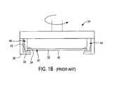
- a carrier headAs shown in FIG. 1A , a conventional carrier head 10 having a rotatable shaft 12 holds a wafer 14 during the electrodeposition process.
- the wafer 14is placed on a surface 16 of a carrier base 18 (chuck) of the carrier head 10 .
- the carrier head 10secures the wafer 14 to the surface 16 of the base 18 of the carrier head 10 by applying vacuum to the back of the wafer and using clamps 20 .
- the vacuumis applied using vacuum lines 22 extending through the carrier base 18 and the body of the carrier head 10 .
- Clamps 20may also seal electrical contacts 24 to the wafer 14 .
- no deposition or material removaloccurs at the edge of the wafer.
- the carrier headis immersed into a solution, typically an electrolyte in a deposition and certain material removal processes, or a slurry in a CMP material removal process, for example.
- a solutiontypically an electrolyte in a deposition and certain material removal processes, or a slurry in a CMP material removal process, for example.
- a padwill be included.
- leakages to the backside of the wafercontaminate the wafer backside and the electrical contacts. Removal of contaminants from the wafer backside requires an extra process step that is time consuming and increases manufacturing costs.
- FIG. 1BAnother conventional wafer carrier design does not use vacuum suction on the back of the wafer to retain the wafer on the carrier and attempts to reduce contamination of the wafer backside and wafer edge during processing.
- the back surface 30 of the wafer 32is pressed against an o-ring 34 to form a seal between the back surface 30 of the wafer and the o-ring 34 .
- a clamp 36 including a seal 38seals a perimeter of the front surface 40 of the wafer 32 while housing the plurality of contacts 42 to the front surface 40 .
- a region 44 behind the sealcan be pressurized with gas to further prevent contamination at the wafer backside. In such designs, because of the clamp around the periphery of the wafer, no deposition or material removal occurs at the edge of the wafer.
- Yet another conventional CMP headis similar to the head shown in FIG. 1A , but it holds the wafer from the back side by vacuum when positioning the wafer for processing and from the circumference of the wafer by a retaining ring during processing, thereby fully exposing the front surface of the wafer. While the CMP process is done over the front surface of the wafer, the slurry from the CMP process can nevertheless migrate toward the back surface of the wafer.
- the present inventionattains the above objects, considered singly or in combination, among others, by providing a wafer carrier that includes a plurality of concentric sealing members to provide a better seal, with the outer seal preferably being independently vertically movable to allow cleaning of a peripheral backside of the wafer to occur while the wafer is still attached to the wafer carrier and a plurality of vacuum openings that are disposed only adjacent to an inner side of the inner seal at a location corresponding to the backside periphery of the wafer.
- a sealing memberwhich is alternatively an o-ring, gasket, or inflatable member is used in combination with the vacuum holes positioned as described above to assist in preventing the processing liquids and contaminants resulting therefrom from reaching the backside inner region of the wafer as well as minimize irregularities in polishing that are caused by using a vacuum to attach a backside of a wafer to a wafer carrier.
- sealing mechanismhaving at least three annularly disposed sealing members is described.
- the above-described characteristics of the wafer carriercan be used on different wafer carriers that are used in various processing environments.
- FIGS. 1A and 1Billustrate various conventional carrier heads
- FIG. 2illustrates an exemplary processing system on which carrier heads according to the present invention may be used.
- FIGS. 3A and 3Billustrate more detailed views of wafer carriers according to two embodiments of the present invention
- FIGS. 4A and 4Billustrate injected gas and process fluid flow using the wafer carriers according the two embodiments illustrated in FIGS. 3A and 3B of the present invention
- FIG. 5illustrates a gasket member used in the embodiment of the present invention illustrated in FIGS. 3B and 4B ;
- FIGS. 6A and 6Billustrate usage of the gasket member illustrated in FIG. 5 in more detail
- FIGS. 7A and 7Billustrate another embodiment of a the present invention using an inflatable gasket member
- FIGS. 8A-8Dillustrate another embodiment of the present invention using a pair of concentric gasket members
- FIGS. 9A-9Cillustrate another embodiment of the present invention using a pair of concentric gasket members
- FIGS. 10A-10Cillustrate another embodiment of the present invention using a pair of concentric gasket members that are positioned at a periphery of the backside of the wafer and vacuum openings that are only adjacent an inner region of the inner gasket member;
- FIGS. 11A-11Cillustrate a method of creating various carriers using a replaceable support pad
- FIGS. 12A-12Billustrates other embodiments in which a thin, expandable membrane is used to protect between annular housings.
- FIG. 2shows an exemplary processing system 100 .
- the system 100may, for example, include a cathode assembly 102 and an anode assembly 104 and can then deposit a conductive material such as copper on a workpiece or substrate, such as semiconductor wafer.
- the system 100may, for example, have the polarity of the anode and cathode reversed, or instead use other processing chemicals.
- the wafer carrier described hereincan be used in a CMP process with CMP solutions, such as a CMP slurry. It should be understood that the particular process in which the present invention is used is not of particular importance. What is significant, as illustrated hereinafter, is prevention of contamination of a processing solution from reaching a backside of a wafer. And in certain embodiments, also allowing for full face processing of the wafer to occur.
- the wafer holding assembly 102 of the system 100includes a wafer carrier 106 , shown in FIG. 2 holding an exemplary wafer 108 , which can be referred to as the cathode during deposition, the anode during electropolishing, or just the wafer if a process that does not require a current flow/voltage differential to exist.
- a front surface 112 of the wafer 108is connected to a negative terminal of a power supply (not shown) by electrical contact members 114 .
- electropolishingfor example, the front surface 112 of the wafer 108 is connected to a positive terminal of a power supply (not shown) by electrical contact members 114 .
- the wafer carrier 106holds the wafer 108 from a back surface 113 of the wafer 108 using vacuum suction.
- the wafer 108is held by the wafer carrier 106 so that a front surface 112 of the wafer 108 is fully exposed.
- the wafer carrier 106 and hence the wafer 108are moved by rotating a carrier shaft 110 about a rotation axis 115 or vertical axis and/or by laterally translating the carrier shaft 110 .
- the electrode assembly 104 of the system 100will typically have a different type of electrode 116 , depending upon whether assembly 104 is being used for deposition or electropolishing.
- the electrode 116is an anode, preferably a consumable copper anode, and when used for electropolishing, the electrode 116 is a cathode, and is preferably not consumable.
- the electrode 116may preferably be placed into an enclosure such as an electrode cup 118 .
- the electrode 116may have holes that allow the electrolyte to flow therethrough (not shown).
- the electrode cup 118may have bleeding openings (not shown) to control the amount of the flow of solution, such as electrolyte when used for deposition and certain electropolishing techniques, or slurry if CMP is being used, for example.
- the solution 120is pumped into the electrode cup 118 through a liquid inlet 130 to reach and wet the front surface 112 of the wafer 108 .
- the solution 120flows in the direction of arrows and wets the front surface 112 of the wafer 108 .
- the solution 120is an electrolyte that is used to deposit material on the front surface 112 of the wafer 108 under applied appropriate potential or remove material from the front surface 112 of the wafer 108 under applied appropriate potential.
- the wafer front surface 112is preferably rotated as is known.
- electrical contact members 114contact wafer 108 on a contact region 126 , as shown in FIG. 2 .
- the contact region 126is a peripheral ring region on the front surface of the wafer that has a portion thereof that is always exposed over the edge of the electrode cup 118 as the wafer is rotated.
- FIGS. 3A and 3Beach illustrate a side view with a cut-away of the wafer carrier 106 of embodiments of the present invention in further detail. As will become apparent, the difference between the embodiments illustrated in FIGS. 3A and 3B is the type of sealing member 154 that is used.
- the wafer carrier 106comprises a carrier body 140 having a lower and upper end 142 and 144 .
- the lower end 142 of the carrier 106comprises a carrier base 146 , chuck, upon which the wafer 108 is held.
- the carrier basemay be made of variety of materials, such as plastic, steel or titanium.
- the carrier ring 147can have a surface portion that extends below the surface of the wafer that contacts the support pad 166 described further below to prevent lateral movement of the wafer 108 beyond the surface portion that extends below the backside surface of the wafer 108 .
- the carrier base 146is preferably surrounded by a carrier ring 147 .
- the carrier ringmay be constructed separately or may be an integral part of the carrier base.
- the carrier ringmay be made of plastic or any material that is stable in the process solutions.
- the wafer carrier 106is rotated or moved through the shaft 110 .
- a bottom surface 148 of the carrier base 146preferably disk shaped, includes a first surface portion 150 and a second surface portion 152 .
- the first surface portion 150is a peripheral surface surrounding the second surface portion 152 that is an inner region.
- the first and second surface portions 150 , 152 of the bottom surface 148are established by a sealing member 154 of the present invention, described hereinafter.
- the sealing member 154is placed into a circular groove 156 formed in the bottom surface 148 and between the first and second surfaces 150 , 152 defines an inner region of the base 146 , and, when the sealing member 154 contacts the back side of the wafer 108 , establishes a backside inner region of the wafer 108 .
- Fluid lines 158connect a fluid supply to a plurality of outlet ports 159 on the first surface portion 150 of the bottom surface 148 , as described further hereinafter.
- the outlet ports 159are radially distributed around the first surface 150 , such that the outlet ports are formed concentrically around the sealing member 154 .
- a lower end 160 of the fluid lines 158may run between the carrier base 146 and the carrier ring 147 .
- the fluid lines 158are used to blow a gas, preferably a non-oxidizing gas, onto a peripheral back edge 162 of the back surface 113 of the wafer 108 .
- the non-oxidizing gasmay preferably be nitrogen gas.
- Holesmay have any number and varied diameters, but preferably a diameter in the range of 0.5-1 mm found most preferable. In the preferred embodiment, at 16-64 holes are disposed around the edge of the wafer carrier, for wafer sizes of between 200 and 300 mm.
- the number of such holescan vary, and, instead of holes, a continuous slit or slits, or another shaped opening can be used instead.
- the gas flow ratecan vary, with a flow rate preferably between 10-60 liters per minute.
- the gas emitted from ports 159continuously sweeps the peripheral back edge 162 and provides another seal that assists in preventing liquid, such as electrolyte, from reaching behind the wafer 108 and causing unwanted contamination.
- the wafer 108is retained by the carrier base 146 by the application of vacuum suction.
- a number of vacuum lines 164are connected to the second surface 152 of the carrier base 146 .
- a support pad 166 or a backing padis preferably, but not necessarily, attached on the second surface portion 152 to maintain the wafer in a substantially flat state while under the applied vacuum suction.
- the vacuum lines 164continue through holes in the support pad 166 .
- the wafermay be held using a suction cup.
- the sealing member 154In order for the seal to be created, the sealing member 154 must extend past the support pad 166 , typically by an amount that is in the range of 50-100 microns, so that the seal can be properly formed. As described hereinafter, the sealing member 154 will be relatively much softer than the support pad 166 .
- the other componentssuch as mechanical components of the wafer carrier 106 may be conventionally constructed and well known in the art.
- the carrier head 106may be provided with some form of gimbal mechanism and cooperating mechanical components. Such conventional components need not be further described.
- the wafer 108is placed on the carrier base 146 as shown in FIGS. 3A and 3B , using a wafer handling system (not shown).
- the wafer 108is aligned with the sealing member 154 and under the applied vacuum, the sealing member 154 seals the space confined between the second surface portion 152 and the back 113 of the wafer, thereby retaining the wafer 108 on the wafer carrier 106 and fully exposing the front surface 112 of the wafer 108 .
- vacuum levels in the range of 400-650 Torrwere employed.
- gasis blown through the ports 159 onto the peripheral back edge 162 as the wafer is processed during deposition, in an amount as described above.
- the gas flow from the ports 159in the direction of the arrow 168 , sweeps away the electrolyte 120 flowing in the direction of the arrow 170 (delivered to the frontside of the wafer 108 through pad 200 that contains channels 202 therein) and assists in preventing the electrolyte solution from reaching the peripheral back edge 162 of the wafer 108 .
- the wafer carrier of the present inventionadvantageously prevents the electrolyte from reaching the back surface 113 of the wafer 108 while rotating the wafer 108 relative to the pad 200 and fully exposing the front surface 112 of the wafer to the processing solutions.
- the sealing member 154is designed such that the sealing function is efficiently achieved with the application of minimum vacuum suction.
- the sealing member 154 A illustrated in FIGS. 3A and 4Ais an o-ring made of an insulating material.
- the o-ring 154 Amay or may not be hollow inside, but as shown in FIG. 4A , it will tend to retain its shape under pressure. It has been found that preferably the o-ring 154 A is hollow, having a diameter of 1-4 mm, and a thickness of between 0.5 and 1.5 mm.
- the hollow o-ringthere is softness to the hollow o-ring, such that it has a durometer rating of less than 70, and preferably within the range of 30-50 durometers, in contrast to typical o-rings that are much harder, and have a higher durometer rating, and support pads 166 that will have a durometer rating (which is a hardness rating) that typically are at least 5 times greater than that of the hollow o-ring.
- This softnessadvantageously allows for the desired seal to occur, without the detrimental side effect of causing bowing on the wafer due to the pressure of a hard seal exerting too much pressure onto the backside of the wafer.
- the o-ring 154 Aparticularly when hollow, is preferably made of an ethylene propylene material.
- the gasket 154 B illustrated in FIGS. 3B and 4Bis an alternative to the o-ring 154 A.
- the gasket 154 Bhas a circular body 300 having a bulb shape cross section.
- the body 300has a first portion 302 or an attachment portion and a second portion 304 or a sealing portion.
- the sealing portion 304may preferably be slanted outwardly to offer more sealing surface when the vacuum is applied, which will be described more fully below.
- FIG. 6Ashows the gasket 154 B in cross section and with no compressive force applied upon it or no wafer held on it.
- the gasket 154 Bis placed on the wafer carrier by inserting the attachment portion 302 into the circular groove 156 .
- the sealing portion 304 of the gasket 154 Bdefines a sealing surface 306 which is a slanted surface generally facing the back surface 113 of the wafer 108 .
- the sealing portion 304is a compression distance, denoted with ‘h’, higher than the top of the support pad 166 .
- the compression distancemay be in the range of 0.1 mm to 0.3 mm, preferably 0.2 mm. In sealing stage, the compression distance ‘h’ is reduced to zero, allowing full usage of the sealing surface 306 .
- FIG. 6Bshows the gasket 154 B when sealing the back surface 113 of the wafer 108 .
- the wafer 108presses against the sealing surface 306 and causes the sealing portion 304 to collapse thereby achieving sealing function.
- the gasket 154 Bachieves sealing function with ease, i.e., by the collapse of the sealing portion 306 and with providing larger sealing surface.
- the gasket 154 Bcan be made of an elastic material such as elastomer.
- an elastic materialsuch as elastomer.
- KalrezTMwhich can be available from DuPont. It is understood, however, that although in the preferred embodiment the gasket member of the present invention is described above, the gasket member may be made of any compressible material, membrane, or tube, or the like, as long as it performs the above given sealing functions, and is within the scope of the present invention.
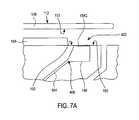
- a gasket member 154 Cmay be an inflatable membrane.
- FIG. 7Ashows the inflatable membrane in deflated stage.
- the inflatable membrane 154 Cis attached to and seals the perimeter edge of opening 402 of the circular grove 156 .
- the circular grooveis connected to a fluid line 404 through at least one inlet port 406 so that a fluid such as air can be used to inflate the inflatable membrane 154 C.
- the fluid line 404is further connected to a fluid supply system (not shown) such that the fluid pressure can be controlled.
- FIG. 7Bshows the inflatable member 154 C in inflated stage and when sealing the back surface 113 of the wafer 108 .
- the wafer 108presses against the inflatable membrane thereby achieving sealing function.
- the inflatable member 154 Cmay be made of any rubber or elastomer material.
- FIGS. 8A-8Dillustrate another embodiment of the present invention using a pair of concentric sealing members.
- a carrier head 500comprises a carrier body 502 and a carrier base 504 where a wafer or other workpiece 505 is held.
- the carrier head 500is rotated or moved through the shaft 508 .
- the carrier base 504comprises a bottom surface 506 that is preferably a surface that conforms to the shape of the workpiece, typically circular for a wafer.
- a first sealing member 508 and a second sealing member 509are concentrically placed adjacent outer circumference 510 of the bottom surface 506 .
- the first sealing member 508is preferably an inflatable gasket membrane having a circular strip shape.
- the membrane 508is attached to the bottom surface 506 of the carrier base 504 from its inner and outer circumferential edges 512 and 514 , respectively, such that an inner pocket 516 of the membrane 508 is formed.
- the inner pocket 516 of the membrane 508is connected to a fluid source (not shown), such as a gas source, through fluid lines 518 .
- a fluid sourcenot shown
- the fluid from the fluid lines 518is used to inflate the inflatable membrane 508 during the process.
- the second sealing member 509is preferably made such as one of the sealing members 154 described above. In a particularly preferred embodiment, the second sealing member is made as the hollow o-ring 154 A as described in FIGS.
- the second sealing member 509is preferably placed in a circular groove 520 .
- a support member 522may be concentrically placed within the circular area formed by the o-ring 509 .
- a number of vacuum lines 524are formed through the carrier base 504 and through the support member 522 so that when the wafer 505 is placed on the support member 522 , vacuum suction can be created on back side 526 of the wafer 505 , which is sealed by the second sealing member 509 .
- the back side 526 of the wafer 505is placed on the o-ring 509 and vacuum suction is applied to hold the wafer 505 on the carrier 500 . It is understood that in this embodiment, front surface 528 of the wafer 505 is fully exposed.
- the inflatable membrane 508is inflated by supplying gas into the inner pocket 516 . In inflated state the inflatable membrane 509 effectively seals edge region 530 of the wafer 505 .
- both the inflatable membrane 508 and the o-ring 509form a double seal along the circumference/edge of the wafer 505 .
- Such combinationadvantageously prevents leakage of the process solutions, such as electrolyte, through both the inflatable member 508 , and the o-ring 509 and prevents contamination of the backside 526 of the wafer as well as of the support member 522 .
- this edge region 530can be easily cleaned, such as during a cleaning step after a plating step, as explained hereinafter.
- the first sealing member 508is preferably an inflatable member.
- the first sealing member 508when an inflatable member, can be deflated, as shown. This exposes a potentially contaminated edge region 530 while the wafer is still being held by the carrier 500 and the vacuum suction is still being applied to the area sealed by the o-ring 509 .
- cleaning of the edge region 530can occur by applying a cleaning fluid or fluids (such as either a liquid cleaning fluid, or both a liquid cleaning fluid and thereafter a gas such as air for drying) in the direction of arrow 5 into the edge region 530 from a cleaning system (not shown) into the area that had previously been protected to the inflated inflatable member 508 .
- a cleaning fluid or fluidssuch as either a liquid cleaning fluid, or both a liquid cleaning fluid and thereafter a gas such as air for drying
- the carrier 500may also be spun.
- the first sealing member 508is preferably an inflatable membrane, for the reasons described above, other alternative seals, for example an o-ring, can also be used.
- FIGS. 9A-9Cillustrate another embodiment of the present invention using a pair of concentric gasket members.
- This embodimentis similar to the FIG. 8 embodiment, as shown in the overview of FIG. 9A , in using a first seal member 908 and a concentric second seal member 909 to provide a seal for the backside of the wafer 905 within the interior region formed by the second seal member 909 , which interior region includes a support member 922 .
- the backside of the wafer 905is preferably held on the second sealing member 909 and the support member 922 through the usage of a vacuum that is applied through vacuum lines 924 .
- FIG. 9A-9Cillustrate another embodiment of the present invention using a pair of concentric gasket members.
- This embodimentis similar to the FIG. 8 embodiment, as shown in the overview of FIG. 9A , in using a first seal member 908 and a concentric second seal member 909 to provide a seal for the backside of the wafer 905 within the interior region formed by the second seal member 909 ,
- the first sealing member 908is preferably an o-ring, which may or may not be hollow inside, but preferably has a softness that is softer than that of the second sealing member 909 .
- the seal with the first sealing member 908is also formed by having a vertically moveable annular housing 904 on the outside of the carrier head 900 .
- the vertical movabilitycan be achieved in a variety of manners, including a motorized sprocket along the inner radius of the annular housing 904 , other mechanical mechanisms, or otherwise.
- FIG. 9Billustrates in more detail the sealed position, in which both the first seal member 908 and the second seal member 909 provide the sealing function.
- the vertically moveable annular housing 904is moved downward, to establish the seal between the first sealing member 908 and the wafer 905 .
- the waferis processed in the chemical environment when both sealing members 908 and 909 seal the wafer 905 .
- there is no carrier ring with a surface portion that extends below the backside surface of the wafer 905as is shown in FIG. 3A , to assist in preventing lateral movement of the wafer 905 , and thus, the vacuum applied through vacuum lines 924 is solely used to prevent lateral movement of the wafer 905 relative to the carrier head 900 .
- the vertically moveable annular housingIn the unsealed position, which allows a cleaning fluid, or gas, to be injected into the backside of the wafer outside of the second sealing member 909 , as shown by the arrows in FIG. 9C , the vertically moveable annular housing is moved upward, thereby disengaging the first sealing member 908 and providing a gap through which the cleaning fluid or gas can be injected to the peripheral backside of the wafer 905 , outside of the second sealing member 909 .
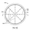
- FIGS. 10A-Billustrate another embodiment of the present invention using a pair of concentric seal members 1008 and 1009 that are positioned at a periphery of the backside of the wafer 1005 and vacuum openings 1025 that are only adjacent an inner region of the inner seal member 1009 . No such openings 1025 are located in further within the inner region of the wafer 1005 .
- This embodimentis similar to the FIG. 9 embodiment, as shown in the overview of FIG. 10A , in using a first seal member 1008 and a concentric second seal member 1009 to provide a seal for the backside of the wafer 1005 within the interior region formed by the second seal member 909 , which interior region includes a support member 1022 .
- the backside of the wafer 1005is preferably held on the second sealing member 1009 and the support member 1022 through the usage of a vacuum that is applied through vacuum lines 1024 , except that the vacuum openings 1025 are only adjacent an inner region of the inner seal member 1009 .
- the vacuum lines 1024can be formed in a variety of manners, with either independent lines to each vacuum opening, but more preferably using a plurality of grooves 1026 that are formed in a bottom surface 1058 of the carrier base 1046 , which grooves have disposed thereover the support pad 1022 , which support pad has the openings 1025 disposed at locations at the periphery as mentioned above, which each align with a groove 1026 .
- each of the grooves 1026forms a portion of the vacuum line 1024 . It is noted that it is preferable for each of the grooves 1026 to terminate at its outer end 1026 A such that the vacuum therefrom is not applied to the second sealing member 1009 .
- FIG. 10Billustrates in more detail the sealed position, in which both the first seal member 1008 and the second seal member 1009 provide the seal.
- the vertically moveable annular housing 1004is moved downward, to establish the seal between the first sealing member 1008 and the wafer 1005 .
- the waferis processed in the chemical environment when both sealing members 1008 (which is disposed on the annular housing 1004 ) and 1009 seal the wafer 1005 . It is noted that there is no carrier ring with a surface portion that extends below the backside surface of the wafer 1005 , as is shown in FIG.
- the vacuum applied through vacuum lines 1024 to the vacuum openings 1025 that are adjacent the inner region of the sealing member 1009is solely used to prevent lateral movement of the wafer 1005 relative to the carrier head 1000 .
- the vertically moveable annular housing 1004 shown in FIG. 10Bis moved upward just as the annular housing 904 is moved upward as illustrated in FIG. 9C , thereby disengaging the first sealing member 1008 and providing a gap through which the cleaning fluid or gas can be injected to the peripheral backside of the wafer 1005 , outside of the second sealing member 1009 .
- a modification of the embodiment illustrated in FIGS. 10A and 10Bwhich will provide sealing without certain of the cleaning advantages, is to use only a single seal, such as the sealing member 1009 , without an outer annular housing 1004 or the first sealing member 1008 .
- irregularities in polishingthat are caused by using a vacuum to attach the backside of a wafer 1105 to the wafer carrier head 1100 are minimized.
- FIG. 10Cillustrates another support plate 1022 A, which support plate is modified from the support plate 1022 illustrated in FIGS. 10A-B , and, as will be described herein, thus allows a method to efficiently configure a wafer carrier head to obtain a desired vacuum opening arrangement.
- the peripheral openings 1025are made in the support pad 1022 , and the support pad 1022 attached to a bottom surface 1058 of the carrier base 1046 , such as by using an adhesive, such that the grooves 1026 along with the support pad 1022 disposed thereover, will form the vacuum lines 1024 .
- the openings 1025 within the support pad 1022 at peripheral locations corresponding to the grooves 1126are then used to create the local pressure only at the periphery of the wafer 1005 , as described above with reference to FIGS. 10A-B .
- openings 1025are instead desired at various locations over the entire backside surface of the wafer 1005 , then, as illustrated in FIG. 10C , openings 1025 A that are disposed within the inner region of the support pad 1022 A that also intersect with the grooves 1126 can be formed for the creation of local pressure at each such location.
- the same workpiece carrier 1000can have one support pad 1022 with openings 1025 in one set of locations that is then taken off, with another support pad 1022 A subsequently added that has openings 1025 A in different locations, to change the local vacuum profile by only changing the support pad 1022 .
- any other type of supportsuch as a hard inert metal surface obtained from a plate with openings that correspond to the grooves as noted above could also be used to establish the surface that contacts the wafer and allow for the openings, in the desired configurations as discussed above, to exist that will provide the local vacuum profile.
- grooves in conjunction with a support padare described as one manner of providing a pathway for the pressure to the openings, any variety of ways could be used to establish the pathway.
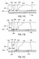
- FIGS. 11A-11Cillustrates another preferred embodiment, which provides a multi-stage seal. For purposes of description, three stages are illustrated, and preferably only three stages are used, although more stages could be added if desired.
- FIG. 3in addition to the annular housing 1104 containing the second seal member 1108 , which annular housing 1104 and seal 1108 correspond to the annular housing 904 and seal 908 illustrated in FIG. 9 , there is included another annular housing 1106 with a third seal member 1107 , which can move vertically with respect to the wafer 1105 independently of the movement of the annular housing 1104 . It is noted, however, that two or more annular housings, such as 1104 and 1106 , can, particularly if more than three annular housings are used, be moved together in synchronism.
- the wafer 1105 illustrated in FIG. 11Ais attached to the wafer carrier 1100 using a vacuum and the three seal members 1107 , 1108 and 1109 , based upon the same principles as described above. Once attached, the frontside of the wafer 1105 can be processed. As a result of processing, chemical deposits from the processing will build up in the area 1150 as shown.
- cleaning the wafer 1105can be initiated, which cleaning will include directing a cleaning solution to the backside of the wafer to clean away residue 1150 after the annular housing 1106 has been moved away from the wafer 1105 to break the seal between the seal member 1107 and the wafer 1105 as described above.
- the waferwill be rotated by the wafer carrier 1100 while the cleaning solution is directed to the bevel edge of the wafer 1105 .
- the wafer 1105can continue to be rotated to dry substantially the entire surface of the wafer 1105 . As shown in FIG. 11B , however, a small amount of residual cleaning solution will typically remain at location 1160 where the seal between the sealing member 1108 and the wafer 1105 exists. If the embodiment described in FIG. 9 was used, this small amount of cleaning solution would remain where the seal 909 contacts the wafer 905 , which small amount would remain even after spin drying the wafer 905 . In this embodiment, as shown in FIG. 11C , with the multi-stage seal, the seal 1108 can be broken with the wafer 1105 by moving the annular housing 1104 .
- any residual cleaning solution 1160 that remains on the wafer 1105can be removed by spin drying the wafer 1105 . With no residual cleaning solution on the wafer 1105 , when the seal 1109 is thereafter broken and the wafer 1105 removed, it will have dried with no residual cleaning solution thereon.
- the vacuum suctioncan be eliminated and pressure applied through the vacuum lines or openings, such as vacuum line 1124 illustrated.
- an annular housingsuch as annular housing 1106
- an annular housing 1106that ha has previously been raised can be lowered, such that the associated seal, such as sealing member 1107 , will touch the wafer 1105 , and pressure from the annular housing 1106 can be applied to assist in removing the wafer 1105 from the wafer carrier.
- the vacuum suctioncan be eliminated, and then the force from the annular housing, such as annular housing 1106 , can be used to remove the wafer 1105 from the wafer carrier.
- movable annular housingsare illustrated as being used to create the intermittently permanent sealing, other intermittent permanent seals can be used, such as the inflatable membrane described previously with respect to FIGS. 8A-8C .
- FIG. 12Aillustrates another embodiment in which a thin, expandable membrane is used to protect between annular housings.
- FIG. 12uses the same reference designations as FIG. 11A , and further illustrates thin, expandable membranes 1130 and 1132 , made from a material such as rubber, or from the same material that is used to make the seal.
- These membranes 1130 and 1132are shown as being attached between adjacent o-rings 1107 and 1108 , and also 1108 and 1109 respectively. They can also be attached at any location between adjacent annular housings, and are used to protect the areas between adjacent annular housings such as 1134 and 1136 as shown.
- These membranescan be used with our without the support pad 1122 being located between the adjacent o-rings, or other types of adjacent sealing members.
- eachis preferably coated with a material that allows for chemical compatibility with the process being performed, such as Teflon® for chemical compatibility with plating that uses an electrolyte as well as cleaning with conventional cleaning solutions.
Landscapes
- Engineering & Computer Science (AREA)
- Chemical & Material Sciences (AREA)
- Organic Chemistry (AREA)
- Metallurgy (AREA)
- Materials Engineering (AREA)
- Electrochemistry (AREA)
- Chemical Kinetics & Catalysis (AREA)
- Computer Hardware Design (AREA)
- Power Engineering (AREA)
- Microelectronics & Electronic Packaging (AREA)
- Physics & Mathematics (AREA)
- Manufacturing & Machinery (AREA)
- General Physics & Mathematics (AREA)
- Condensed Matter Physics & Semiconductors (AREA)
- Life Sciences & Earth Sciences (AREA)
- Sustainable Development (AREA)
- Mechanical Engineering (AREA)
- Container, Conveyance, Adherence, Positioning, Of Wafer (AREA)
- Weting (AREA)
- Electroplating Methods And Accessories (AREA)
Abstract
Description
Claims (48)
Priority Applications (6)
| Application Number | Priority Date | Filing Date | Title |
|---|---|---|---|
| US10/159,295US6939206B2 (en) | 2001-03-12 | 2002-05-31 | Method and apparatus of sealing wafer backside for full-face electrochemical plating |
| TW092114826ATW200401390A (en) | 2002-05-31 | 2003-05-30 | Method and apparatus of sealing wafer backside for full-face electrochemical plating |
| PCT/US2003/017228WO2003103025A2 (en) | 2002-05-31 | 2003-05-30 | Method and apparatus of sealing wafer backside for full-face electrochemical plating |
| JP2004510014AJP2005528794A (en) | 2002-05-31 | 2003-05-30 | Method and apparatus for sealing the back side of a wafer for full surface electrochemical plating |
| AU2003238863AAU2003238863A1 (en) | 2002-05-31 | 2003-05-30 | Method and apparatus of sealing wafer backside for full-face electrochemical plating |
| KR1020047019506AKR20050033553A (en) | 2002-05-31 | 2003-05-30 | Method and apparatus of sealing wafer backside for full-face electrochemical plating |
Applications Claiming Priority (3)
| Application Number | Priority Date | Filing Date | Title |
|---|---|---|---|
| US27540601P | 2001-03-12 | 2001-03-12 | |
| US09/910,686US6855037B2 (en) | 2001-03-12 | 2001-07-20 | Method of sealing wafer backside for full-face electrochemical plating |
| US10/159,295US6939206B2 (en) | 2001-03-12 | 2002-05-31 | Method and apparatus of sealing wafer backside for full-face electrochemical plating |
Related Parent Applications (1)
| Application Number | Title | Priority Date | Filing Date |
|---|---|---|---|
| US09/910,686Continuation-In-PartUS6855037B2 (en) | 2001-03-12 | 2001-07-20 | Method of sealing wafer backside for full-face electrochemical plating |
Publications (2)
| Publication Number | Publication Date |
|---|---|
| US20030008602A1 US20030008602A1 (en) | 2003-01-09 |
| US6939206B2true US6939206B2 (en) | 2005-09-06 |
Family
ID=29709664
Family Applications (1)
| Application Number | Title | Priority Date | Filing Date |
|---|---|---|---|
| US10/159,295Expired - LifetimeUS6939206B2 (en) | 2001-03-12 | 2002-05-31 | Method and apparatus of sealing wafer backside for full-face electrochemical plating |
Country Status (6)
| Country | Link |
|---|---|
| US (1) | US6939206B2 (en) |
| JP (1) | JP2005528794A (en) |
| KR (1) | KR20050033553A (en) |
| AU (1) | AU2003238863A1 (en) |
| TW (1) | TW200401390A (en) |
| WO (1) | WO2003103025A2 (en) |
Cited By (20)
| Publication number | Priority date | Publication date | Assignee | Title |
|---|---|---|---|---|
| US20050202765A1 (en)* | 2004-03-05 | 2005-09-15 | Strasbaugh | Independent edge control for CMP carriers |
| US20070261907A1 (en)* | 2006-05-01 | 2007-11-15 | Yamaha Hatsudoki Kabushiki Kaisha | Exhaust device and vehicle with exhaust device |
| US20080043334A1 (en)* | 2006-08-18 | 2008-02-21 | Mirage Innovations Ltd. | Diffractive optical relay and method for manufacturing the same |
| EP1942364A1 (en) | 2005-09-14 | 2008-07-09 | Mirage Innovations Ltd. | Diffractive optical relay and method for manufacturing the same |
| US20080166952A1 (en)* | 2005-02-25 | 2008-07-10 | Shin-Etsu Handotai Co., Ltd | Carrier For Double-Side Polishing Apparatus, Double-Side Polishing Apparatus And Double-Side Polishing Method Using The Same |
| US20090093127A1 (en)* | 2003-11-26 | 2009-04-09 | Stephan Bradl | Treatment of a Substrate with a Liquid Medium |
| US20090097122A1 (en)* | 2005-09-14 | 2009-04-16 | Mirage Innovations Ltd | Diffractive Optical Device and System |
| US20090128902A1 (en)* | 2005-11-03 | 2009-05-21 | Yehuda Niv | Binocular Optical Relay Device |
| US20090203300A1 (en)* | 2004-03-09 | 2009-08-13 | Speedfam Co., Ltd. | Carrier for holding an object to be polished |
| US20090305615A1 (en)* | 2006-07-18 | 2009-12-10 | Shin-Etsu Handotai Co., Ltd | Carrier for double-side polishing apparatus, double-side polishing apparatus using the same, and double-side polishing method |
| US20100178202A1 (en)* | 2006-06-16 | 2010-07-15 | Shigemi Isobe | Fluidized-bed apparatus |
| US20100177388A1 (en)* | 2006-08-23 | 2010-07-15 | Mirage Innovations Ltd. | Diffractive optical relay device with improved color uniformity |
| US20100302644A1 (en)* | 2007-09-18 | 2010-12-02 | Mirage Innovations Ltd | Slanted optical device |
| US20110104995A1 (en)* | 2008-02-27 | 2011-05-05 | Shin-Etsu Handotai Co., Ltd. | Carrier for a double-side polishing apparatus, double-side polishing apparatus using this carrier, and double-side polishing method |
| USRE42992E1 (en) | 2003-02-19 | 2011-12-06 | Mirage Innovations Ltd. | Chromatic planar optic display system |
| US20120052774A1 (en)* | 2010-08-31 | 2012-03-01 | Norihiko Moriya | Polishing apparatus |
| US20120088366A1 (en)* | 2010-10-05 | 2012-04-12 | Strasbaugh | CMP Retaining Ring with Soft Retaining Ring Insert |
| US20140091537A1 (en)* | 2012-10-02 | 2014-04-03 | Disco Corporation | Chuck table |
| US20170053822A1 (en)* | 2015-08-23 | 2017-02-23 | Camtek Ltd. | Warped wafers vacuum chuck |
| US20170069524A1 (en)* | 2015-09-03 | 2017-03-09 | Disco Corporation | Chuck table |
Families Citing this family (254)
| Publication number | Priority date | Publication date | Assignee | Title |
|---|---|---|---|---|
| JP2006233296A (en)* | 2005-02-25 | 2006-09-07 | Yamamoto Mekki Shikenki:Kk | Fixture for electroplating |
| KR100898793B1 (en)* | 2005-12-29 | 2009-05-20 | 엘지디스플레이 주식회사 | Substrate bonding device for liquid crystal display device |
| US7993457B1 (en)* | 2007-01-23 | 2011-08-09 | Novellus Systems, Inc. | Deposition sub-chamber with variable flow |
| JP5393039B2 (en)* | 2008-03-06 | 2014-01-22 | 株式会社荏原製作所 | Polishing equipment |
| JP5690985B2 (en)* | 2009-12-24 | 2015-04-01 | セイコーエプソン株式会社 | Support apparatus and etching method |
| TWI410527B (en)* | 2010-05-06 | 2013-10-01 | Taiwan Semiconductor Mfg | Electroplating apparatus and method for plating conducting layer on substrate |
| ES2351138B1 (en)* | 2010-05-18 | 2011-11-21 | Viva Developments S.L. | ELECTROMECHANICAL GENERATOR CELL AND PROCEDURE FOR OBTAINING THE SAME |
| JP5775339B2 (en)* | 2011-03-22 | 2015-09-09 | 株式会社Screenホールディングス | Substrate processing equipment |
| AT511627B1 (en)* | 2011-07-01 | 2015-05-15 | Mechatronic Systemtechnik Gmbh | DEVICE FOR HOLDING A SURFACE SUBSTRATE |
| US20130023129A1 (en) | 2011-07-20 | 2013-01-24 | Asm America, Inc. | Pressure transmitter for a semiconductor processing environment |
| NL2009549A (en)* | 2011-10-27 | 2013-05-07 | Asml Netherlands Bv | Lithographic apparatus and substrate handling method. |
| JP6186124B2 (en)* | 2012-12-14 | 2017-08-23 | 東京応化工業株式会社 | Transfer arm, transfer device, and transfer method |
| US20160376700A1 (en) | 2013-02-01 | 2016-12-29 | Asm Ip Holding B.V. | System for treatment of deposition reactor |
| US9353439B2 (en) | 2013-04-05 | 2016-05-31 | Lam Research Corporation | Cascade design showerhead for transient uniformity |
| US10941490B2 (en) | 2014-10-07 | 2021-03-09 | Asm Ip Holding B.V. | Multiple temperature range susceptor, assembly, reactor and system including the susceptor, and methods of using the same |
| US10276355B2 (en) | 2015-03-12 | 2019-04-30 | Asm Ip Holding B.V. | Multi-zone reactor, system including the reactor, and method of using the same |
| NL2014625B1 (en)* | 2015-04-13 | 2017-01-06 | Suss Microtec Lithography Gmbh | Wafer treating device and sealing ring for a wafer treating device. |
| US10023959B2 (en) | 2015-05-26 | 2018-07-17 | Lam Research Corporation | Anti-transient showerhead |
| CN107408530A (en)* | 2015-11-19 | 2017-11-28 | 日本特殊陶业株式会社 | Vacuum chuck |
| US11139308B2 (en) | 2015-12-29 | 2021-10-05 | Asm Ip Holding B.V. | Atomic layer deposition of III-V compounds to form V-NAND devices |
| US10529554B2 (en) | 2016-02-19 | 2020-01-07 | Asm Ip Holding B.V. | Method for forming silicon nitride film selectively on sidewalls or flat surfaces of trenches |
| JP6546550B2 (en)* | 2016-03-09 | 2019-07-17 | 日本特殊陶業株式会社 | Vacuum adsorption member and vacuum adsorption method |
| US10343920B2 (en) | 2016-03-18 | 2019-07-09 | Asm Ip Holding B.V. | Aligned carbon nanotubes |
| US11453943B2 (en) | 2016-05-25 | 2022-09-27 | Asm Ip Holding B.V. | Method for forming carbon-containing silicon/metal oxide or nitride film by ALD using silicon precursor and hydrocarbon precursor |
| JP6789006B2 (en)* | 2016-06-03 | 2020-11-25 | 日本特殊陶業株式会社 | Vacuum suction device |
| JP6725326B2 (en)* | 2016-06-03 | 2020-07-15 | 日本特殊陶業株式会社 | Vacuum chuck and method of manufacturing vacuum chuck |
| US9859151B1 (en) | 2016-07-08 | 2018-01-02 | Asm Ip Holding B.V. | Selective film deposition method to form air gaps |
| US10612137B2 (en) | 2016-07-08 | 2020-04-07 | Asm Ip Holdings B.V. | Organic reactants for atomic layer deposition |
| US9887082B1 (en) | 2016-07-28 | 2018-02-06 | Asm Ip Holding B.V. | Method and apparatus for filling a gap |
| US9812320B1 (en) | 2016-07-28 | 2017-11-07 | Asm Ip Holding B.V. | Method and apparatus for filling a gap |
| US11532757B2 (en) | 2016-10-27 | 2022-12-20 | Asm Ip Holding B.V. | Deposition of charge trapping layers |
| US10714350B2 (en) | 2016-11-01 | 2020-07-14 | ASM IP Holdings, B.V. | Methods for forming a transition metal niobium nitride film on a substrate by atomic layer deposition and related semiconductor device structures |
| US10453726B2 (en) | 2016-11-10 | 2019-10-22 | Applied Materials, Inc. | Electronic device manufacturing load port apparatus, systems, and methods |
| KR102546317B1 (en) | 2016-11-15 | 2023-06-21 | 에이에스엠 아이피 홀딩 비.브이. | Gas supply unit and substrate processing apparatus including the same |
| US11447861B2 (en) | 2016-12-15 | 2022-09-20 | Asm Ip Holding B.V. | Sequential infiltration synthesis apparatus and a method of forming a patterned structure |
| US11581186B2 (en) | 2016-12-15 | 2023-02-14 | Asm Ip Holding B.V. | Sequential infiltration synthesis apparatus |
| US11390950B2 (en) | 2017-01-10 | 2022-07-19 | Asm Ip Holding B.V. | Reactor system and method to reduce residue buildup during a film deposition process |
| US10468261B2 (en) | 2017-02-15 | 2019-11-05 | Asm Ip Holding B.V. | Methods for forming a metallic film on a substrate by cyclical deposition and related semiconductor device structures |
| JP6829118B2 (en)* | 2017-03-16 | 2021-02-10 | 株式会社日本製鋼所 | Laser irradiation device, laser irradiation method, and manufacturing method of semiconductor device |
| US10770286B2 (en) | 2017-05-08 | 2020-09-08 | Asm Ip Holdings B.V. | Methods for selectively forming a silicon nitride film on a substrate and related semiconductor device structures |
| US12040200B2 (en) | 2017-06-20 | 2024-07-16 | Asm Ip Holding B.V. | Semiconductor processing apparatus and methods for calibrating a semiconductor processing apparatus |
| US11306395B2 (en) | 2017-06-28 | 2022-04-19 | Asm Ip Holding B.V. | Methods for depositing a transition metal nitride film on a substrate by atomic layer deposition and related deposition apparatus |
| KR20190009245A (en) | 2017-07-18 | 2019-01-28 | 에이에스엠 아이피 홀딩 비.브이. | Methods for forming a semiconductor device structure and related semiconductor device structures |
| US11374112B2 (en) | 2017-07-19 | 2022-06-28 | Asm Ip Holding B.V. | Method for depositing a group IV semiconductor and related semiconductor device structures |
| US10590535B2 (en) | 2017-07-26 | 2020-03-17 | Asm Ip Holdings B.V. | Chemical treatment, deposition and/or infiltration apparatus and method for using the same |
| TWI815813B (en) | 2017-08-04 | 2023-09-21 | 荷蘭商Asm智慧財產控股公司 | Showerhead assembly for distributing a gas within a reaction chamber |
| US10692741B2 (en) | 2017-08-08 | 2020-06-23 | Asm Ip Holdings B.V. | Radiation shield |
| US10770336B2 (en) | 2017-08-08 | 2020-09-08 | Asm Ip Holding B.V. | Substrate lift mechanism and reactor including same |
| US11769682B2 (en) | 2017-08-09 | 2023-09-26 | Asm Ip Holding B.V. | Storage apparatus for storing cassettes for substrates and processing apparatus equipped therewith |
| US11830730B2 (en) | 2017-08-29 | 2023-11-28 | Asm Ip Holding B.V. | Layer forming method and apparatus |
| US11295980B2 (en) | 2017-08-30 | 2022-04-05 | Asm Ip Holding B.V. | Methods for depositing a molybdenum metal film over a dielectric surface of a substrate by a cyclical deposition process and related semiconductor device structures |
| US10658205B2 (en) | 2017-09-28 | 2020-05-19 | Asm Ip Holdings B.V. | Chemical dispensing apparatus and methods for dispensing a chemical to a reaction chamber |
| US10403504B2 (en) | 2017-10-05 | 2019-09-03 | Asm Ip Holding B.V. | Method for selectively depositing a metallic film on a substrate |
| US10923344B2 (en) | 2017-10-30 | 2021-02-16 | Asm Ip Holding B.V. | Methods for forming a semiconductor structure and related semiconductor structures |
| WO2019103613A1 (en) | 2017-11-27 | 2019-05-31 | Asm Ip Holding B.V. | A storage device for storing wafer cassettes for use with a batch furnace |
| CN111344522B (en) | 2017-11-27 | 2022-04-12 | 阿斯莫Ip控股公司 | Including clean mini-environment device |
| US10872771B2 (en) | 2018-01-16 | 2020-12-22 | Asm Ip Holding B. V. | Method for depositing a material film on a substrate within a reaction chamber by a cyclical deposition process and related device structures |
| KR102695659B1 (en) | 2018-01-19 | 2024-08-14 | 에이에스엠 아이피 홀딩 비.브이. | Method for depositing a gap filling layer by plasma assisted deposition |
| TWI799494B (en) | 2018-01-19 | 2023-04-21 | 荷蘭商Asm 智慧財產控股公司 | Deposition method |
| US11081345B2 (en) | 2018-02-06 | 2021-08-03 | Asm Ip Holding B.V. | Method of post-deposition treatment for silicon oxide film |
| US10896820B2 (en) | 2018-02-14 | 2021-01-19 | Asm Ip Holding B.V. | Method for depositing a ruthenium-containing film on a substrate by a cyclical deposition process |
| WO2019158960A1 (en) | 2018-02-14 | 2019-08-22 | Asm Ip Holding B.V. | A method for depositing a ruthenium-containing film on a substrate by a cyclical deposition process |
| US10731249B2 (en) | 2018-02-15 | 2020-08-04 | Asm Ip Holding B.V. | Method of forming a transition metal containing film on a substrate by a cyclical deposition process, a method for supplying a transition metal halide compound to a reaction chamber, and related vapor deposition apparatus |
| KR102636427B1 (en) | 2018-02-20 | 2024-02-13 | 에이에스엠 아이피 홀딩 비.브이. | Substrate processing method and apparatus |
| US10975470B2 (en) | 2018-02-23 | 2021-04-13 | Asm Ip Holding B.V. | Apparatus for detecting or monitoring for a chemical precursor in a high temperature environment |
| US11473195B2 (en) | 2018-03-01 | 2022-10-18 | Asm Ip Holding B.V. | Semiconductor processing apparatus and a method for processing a substrate |
| KR102646467B1 (en) | 2018-03-27 | 2024-03-11 | 에이에스엠 아이피 홀딩 비.브이. | Method of forming an electrode on a substrate and a semiconductor device structure including an electrode |
| KR102600229B1 (en) | 2018-04-09 | 2023-11-10 | 에이에스엠 아이피 홀딩 비.브이. | Substrate supporting device, substrate processing apparatus including the same and substrate processing method |
| US12025484B2 (en) | 2018-05-08 | 2024-07-02 | Asm Ip Holding B.V. | Thin film forming method |
| US12272527B2 (en) | 2018-05-09 | 2025-04-08 | Asm Ip Holding B.V. | Apparatus for use with hydrogen radicals and method of using same |
| DE102018111858A1 (en)* | 2018-05-17 | 2019-11-21 | Nexwafe Gmbh | Device and method for one-sided etching of a semiconductor layer of a workpiece |
| KR102596988B1 (en) | 2018-05-28 | 2023-10-31 | 에이에스엠 아이피 홀딩 비.브이. | Method of processing a substrate and a device manufactured by the same |
| US11201079B2 (en) | 2018-05-30 | 2021-12-14 | Taiwan Semiconductor Manufacturing Company, Ltd. | Wafer chuck |
| US11718913B2 (en) | 2018-06-04 | 2023-08-08 | Asm Ip Holding B.V. | Gas distribution system and reactor system including same |
| US10797133B2 (en) | 2018-06-21 | 2020-10-06 | Asm Ip Holding B.V. | Method for depositing a phosphorus doped silicon arsenide film and related semiconductor device structures |
| KR102568797B1 (en) | 2018-06-21 | 2023-08-21 | 에이에스엠 아이피 홀딩 비.브이. | Substrate processing system |
| TWI873894B (en) | 2018-06-27 | 2025-02-21 | 荷蘭商Asm Ip私人控股有限公司 | Cyclic deposition methods for forming metal-containing material and films and structures including the metal-containing material |
| KR102854019B1 (en) | 2018-06-27 | 2025-09-02 | 에이에스엠 아이피 홀딩 비.브이. | Periodic deposition method for forming a metal-containing material and films and structures comprising the metal-containing material |
| US10755922B2 (en) | 2018-07-03 | 2020-08-25 | Asm Ip Holding B.V. | Method for depositing silicon-free carbon-containing film as gap-fill layer by pulse plasma-assisted deposition |
| US10388513B1 (en) | 2018-07-03 | 2019-08-20 | Asm Ip Holding B.V. | Method for depositing silicon-free carbon-containing film as gap-fill layer by pulse plasma-assisted deposition |
| US11430674B2 (en) | 2018-08-22 | 2022-08-30 | Asm Ip Holding B.V. | Sensor array, apparatus for dispensing a vapor phase reactant to a reaction chamber and related methods |
| US11024523B2 (en) | 2018-09-11 | 2021-06-01 | Asm Ip Holding B.V. | Substrate processing apparatus and method |
| KR102707956B1 (en) | 2018-09-11 | 2024-09-19 | 에이에스엠 아이피 홀딩 비.브이. | Method for deposition of a thin film |
| CN110970344B (en) | 2018-10-01 | 2024-10-25 | Asmip控股有限公司 | Substrate holding apparatus, system comprising the same and method of using the same |
| KR102592699B1 (en) | 2018-10-08 | 2023-10-23 | 에이에스엠 아이피 홀딩 비.브이. | Substrate support unit and apparatuses for depositing thin film and processing the substrate including the same |
| KR102546322B1 (en) | 2018-10-19 | 2023-06-21 | 에이에스엠 아이피 홀딩 비.브이. | Substrate processing apparatus and substrate processing method |
| US12378665B2 (en) | 2018-10-26 | 2025-08-05 | Asm Ip Holding B.V. | High temperature coatings for a preclean and etch apparatus and related methods |
| US11087997B2 (en) | 2018-10-31 | 2021-08-10 | Asm Ip Holding B.V. | Substrate processing apparatus for processing substrates |
| KR102748291B1 (en) | 2018-11-02 | 2024-12-31 | 에이에스엠 아이피 홀딩 비.브이. | Substrate support unit and substrate processing apparatus including the same |
| US11572620B2 (en) | 2018-11-06 | 2023-02-07 | Asm Ip Holding B.V. | Methods for selectively depositing an amorphous silicon film on a substrate |
| US10818758B2 (en) | 2018-11-16 | 2020-10-27 | Asm Ip Holding B.V. | Methods for forming a metal silicate film on a substrate in a reaction chamber and related semiconductor device structures |
| US12040199B2 (en) | 2018-11-28 | 2024-07-16 | Asm Ip Holding B.V. | Substrate processing apparatus for processing substrates |
| KR102636428B1 (en) | 2018-12-04 | 2024-02-13 | 에이에스엠 아이피 홀딩 비.브이. | A method for cleaning a substrate processing apparatus |
| US11158513B2 (en) | 2018-12-13 | 2021-10-26 | Asm Ip Holding B.V. | Methods for forming a rhenium-containing film on a substrate by a cyclical deposition process and related semiconductor device structures |
| TWI874340B (en) | 2018-12-14 | 2025-03-01 | 荷蘭商Asm Ip私人控股有限公司 | Method of forming device structure, structure formed by the method and system for performing the method |
| TWI866480B (en) | 2019-01-17 | 2024-12-11 | 荷蘭商Asm Ip 私人控股有限公司 | Methods of forming a transition metal containing film on a substrate by a cyclical deposition process |
| TWI845607B (en) | 2019-02-20 | 2024-06-21 | 荷蘭商Asm Ip私人控股有限公司 | Cyclical deposition method and apparatus for filling a recess formed within a substrate surface |
| TWI873122B (en) | 2019-02-20 | 2025-02-21 | 荷蘭商Asm Ip私人控股有限公司 | Method of filling a recess formed within a surface of a substrate, semiconductor structure formed according to the method, and semiconductor processing apparatus |
| TWI838458B (en) | 2019-02-20 | 2024-04-11 | 荷蘭商Asm Ip私人控股有限公司 | Apparatus and methods for plug fill deposition in 3-d nand applications |
| TWI842826B (en) | 2019-02-22 | 2024-05-21 | 荷蘭商Asm Ip私人控股有限公司 | Substrate processing apparatus and method for processing substrate |
| US11742198B2 (en) | 2019-03-08 | 2023-08-29 | Asm Ip Holding B.V. | Structure including SiOCN layer and method of forming same |
| KR102858005B1 (en) | 2019-03-08 | 2025-09-09 | 에이에스엠 아이피 홀딩 비.브이. | Method for Selective Deposition of Silicon Nitride Layer and Structure Including Selectively-Deposited Silicon Nitride Layer |
| JP2020167398A (en) | 2019-03-28 | 2020-10-08 | エーエスエム・アイピー・ホールディング・ベー・フェー | Door openers and substrate processing equipment provided with door openers |
| KR102809999B1 (en) | 2019-04-01 | 2025-05-19 | 에이에스엠 아이피 홀딩 비.브이. | Method of manufacturing semiconductor device |
| KR20200123380A (en) | 2019-04-19 | 2020-10-29 | 에이에스엠 아이피 홀딩 비.브이. | Layer forming method and apparatus |
| KR20200125453A (en) | 2019-04-24 | 2020-11-04 | 에이에스엠 아이피 홀딩 비.브이. | Gas-phase reactor system and method of using same |
| KR20200130121A (en) | 2019-05-07 | 2020-11-18 | 에이에스엠 아이피 홀딩 비.브이. | Chemical source vessel with dip tube |
| KR20200130652A (en) | 2019-05-10 | 2020-11-19 | 에이에스엠 아이피 홀딩 비.브이. | Method of depositing material onto a surface and structure formed according to the method |
| JP7598201B2 (en) | 2019-05-16 | 2024-12-11 | エーエスエム・アイピー・ホールディング・ベー・フェー | Wafer boat handling apparatus, vertical batch furnace and method |
| JP7612342B2 (en) | 2019-05-16 | 2025-01-14 | エーエスエム・アイピー・ホールディング・ベー・フェー | Wafer boat handling apparatus, vertical batch furnace and method |
| USD975665S1 (en) | 2019-05-17 | 2023-01-17 | Asm Ip Holding B.V. | Susceptor shaft |
| USD947913S1 (en) | 2019-05-17 | 2022-04-05 | Asm Ip Holding B.V. | Susceptor shaft |
| KR20200141002A (en) | 2019-06-06 | 2020-12-17 | 에이에스엠 아이피 홀딩 비.브이. | Method of using a gas-phase reactor system including analyzing exhausted gas |
| JP7304742B2 (en)* | 2019-06-06 | 2023-07-07 | 東京エレクトロン株式会社 | Substrate processing equipment |
| KR20200141931A (en) | 2019-06-10 | 2020-12-21 | 에이에스엠 아이피 홀딩 비.브이. | Method for cleaning quartz epitaxial chambers |
| KR20200143254A (en) | 2019-06-11 | 2020-12-23 | 에이에스엠 아이피 홀딩 비.브이. | Method of forming an electronic structure using an reforming gas, system for performing the method, and structure formed using the method |
| KR20210005515A (en) | 2019-07-03 | 2021-01-14 | 에이에스엠 아이피 홀딩 비.브이. | Temperature control assembly for substrate processing apparatus and method of using same |
| JP7499079B2 (en) | 2019-07-09 | 2024-06-13 | エーエスエム・アイピー・ホールディング・ベー・フェー | Plasma device using coaxial waveguide and substrate processing method |
| CN112216646A (en) | 2019-07-10 | 2021-01-12 | Asm Ip私人控股有限公司 | Substrate supporting assembly and substrate processing device comprising same |
| KR20210010307A (en) | 2019-07-16 | 2021-01-27 | 에이에스엠 아이피 홀딩 비.브이. | Substrate processing apparatus |
| KR102860110B1 (en) | 2019-07-17 | 2025-09-16 | 에이에스엠 아이피 홀딩 비.브이. | Methods of forming silicon germanium structures |
| KR20210010816A (en) | 2019-07-17 | 2021-01-28 | 에이에스엠 아이피 홀딩 비.브이. | Radical assist ignition plasma system and method |
| US11643724B2 (en) | 2019-07-18 | 2023-05-09 | Asm Ip Holding B.V. | Method of forming structures using a neutral beam |
| KR20210010817A (en) | 2019-07-19 | 2021-01-28 | 에이에스엠 아이피 홀딩 비.브이. | Method of Forming Topology-Controlled Amorphous Carbon Polymer Film |
| JP6999614B2 (en)* | 2019-07-26 | 2022-01-18 | 株式会社バルカー | Support member |
| TWI851767B (en) | 2019-07-29 | 2024-08-11 | 荷蘭商Asm Ip私人控股有限公司 | Methods for selective deposition utilizing n-type dopants and/or alternative dopants to achieve high dopant incorporation |
| CN112309899A (en) | 2019-07-30 | 2021-02-02 | Asm Ip私人控股有限公司 | Substrate processing apparatus |
| US12169361B2 (en) | 2019-07-30 | 2024-12-17 | Asm Ip Holding B.V. | Substrate processing apparatus and method |
| CN112309900A (en) | 2019-07-30 | 2021-02-02 | Asm Ip私人控股有限公司 | Substrate processing apparatus |
| US11227782B2 (en) | 2019-07-31 | 2022-01-18 | Asm Ip Holding B.V. | Vertical batch furnace assembly |
| US11587814B2 (en) | 2019-07-31 | 2023-02-21 | Asm Ip Holding B.V. | Vertical batch furnace assembly |
| US11587815B2 (en) | 2019-07-31 | 2023-02-21 | Asm Ip Holding B.V. | Vertical batch furnace assembly |
| CN112323048B (en) | 2019-08-05 | 2024-02-09 | Asm Ip私人控股有限公司 | Liquid level sensor for chemical source container |
| CN112342526A (en) | 2019-08-09 | 2021-02-09 | Asm Ip私人控股有限公司 | Heater assembly including cooling device and method of using same |
| USD965044S1 (en) | 2019-08-19 | 2022-09-27 | Asm Ip Holding B.V. | Susceptor shaft |
| USD965524S1 (en) | 2019-08-19 | 2022-10-04 | Asm Ip Holding B.V. | Susceptor support |
| JP2021031769A (en) | 2019-08-21 | 2021-03-01 | エーエスエム アイピー ホールディング ビー.ブイ. | Production apparatus of mixed gas of film deposition raw material and film deposition apparatus |
| USD979506S1 (en) | 2019-08-22 | 2023-02-28 | Asm Ip Holding B.V. | Insulator |
| KR20210024423A (en) | 2019-08-22 | 2021-03-05 | 에이에스엠 아이피 홀딩 비.브이. | Method for forming a structure with a hole |
| KR20210024420A (en) | 2019-08-23 | 2021-03-05 | 에이에스엠 아이피 홀딩 비.브이. | Method for depositing silicon oxide film having improved quality by peald using bis(diethylamino)silane |
| US11286558B2 (en) | 2019-08-23 | 2022-03-29 | Asm Ip Holding B.V. | Methods for depositing a molybdenum nitride film on a surface of a substrate by a cyclical deposition process and related semiconductor device structures including a molybdenum nitride film |
| KR102806450B1 (en) | 2019-09-04 | 2025-05-12 | 에이에스엠 아이피 홀딩 비.브이. | Methods for selective deposition using a sacrificial capping layer |
| KR102733104B1 (en) | 2019-09-05 | 2024-11-22 | 에이에스엠 아이피 홀딩 비.브이. | Substrate processing apparatus |
| US11562901B2 (en) | 2019-09-25 | 2023-01-24 | Asm Ip Holding B.V. | Substrate processing method |
| CN112593212B (en) | 2019-10-02 | 2023-12-22 | Asm Ip私人控股有限公司 | Method for forming topologically selective silicon oxide film by cyclic plasma enhanced deposition process |
| KR20210042810A (en) | 2019-10-08 | 2021-04-20 | 에이에스엠 아이피 홀딩 비.브이. | Reactor system including a gas distribution assembly for use with activated species and method of using same |
| TWI846953B (en) | 2019-10-08 | 2024-07-01 | 荷蘭商Asm Ip私人控股有限公司 | Substrate processing device |
| TW202128273A (en) | 2019-10-08 | 2021-08-01 | 荷蘭商Asm Ip私人控股有限公司 | Gas injection system, reactor system, and method of depositing material on surface of substratewithin reaction chamber |
| TWI846966B (en) | 2019-10-10 | 2024-07-01 | 荷蘭商Asm Ip私人控股有限公司 | Method of forming a photoresist underlayer and structure including same |
| US12009241B2 (en) | 2019-10-14 | 2024-06-11 | Asm Ip Holding B.V. | Vertical batch furnace assembly with detector to detect cassette |
| TWI834919B (en) | 2019-10-16 | 2024-03-11 | 荷蘭商Asm Ip私人控股有限公司 | Method of topology-selective film formation of silicon oxide |
| US11637014B2 (en) | 2019-10-17 | 2023-04-25 | Asm Ip Holding B.V. | Methods for selective deposition of doped semiconductor material |
| KR102845724B1 (en) | 2019-10-21 | 2025-08-13 | 에이에스엠 아이피 홀딩 비.브이. | Apparatus and methods for selectively etching films |
| KR20210050453A (en) | 2019-10-25 | 2021-05-07 | 에이에스엠 아이피 홀딩 비.브이. | Methods for filling a gap feature on a substrate surface and related semiconductor structures |
| US11646205B2 (en) | 2019-10-29 | 2023-05-09 | Asm Ip Holding B.V. | Methods of selectively forming n-type doped material on a surface, systems for selectively forming n-type doped material, and structures formed using same |
| KR20210054983A (en) | 2019-11-05 | 2021-05-14 | 에이에스엠 아이피 홀딩 비.브이. | Structures with doped semiconductor layers and methods and systems for forming same |
| US11501968B2 (en) | 2019-11-15 | 2022-11-15 | Asm Ip Holding B.V. | Method for providing a semiconductor device with silicon filled gaps |
| KR102861314B1 (en) | 2019-11-20 | 2025-09-17 | 에이에스엠 아이피 홀딩 비.브이. | Method of depositing carbon-containing material on a surface of a substrate, structure formed using the method, and system for forming the structure |
| CN112951697B (en) | 2019-11-26 | 2025-07-29 | Asmip私人控股有限公司 | Substrate processing apparatus |
| US11450529B2 (en) | 2019-11-26 | 2022-09-20 | Asm Ip Holding B.V. | Methods for selectively forming a target film on a substrate comprising a first dielectric surface and a second metallic surface |
| CN112885692B (en) | 2019-11-29 | 2025-08-15 | Asmip私人控股有限公司 | Substrate processing apparatus |
| CN120432376A (en) | 2019-11-29 | 2025-08-05 | Asm Ip私人控股有限公司 | Substrate processing apparatus |
| JP7527928B2 (en) | 2019-12-02 | 2024-08-05 | エーエスエム・アイピー・ホールディング・ベー・フェー | Substrate processing apparatus and substrate processing method |
| KR20210070898A (en) | 2019-12-04 | 2021-06-15 | 에이에스엠 아이피 홀딩 비.브이. | Substrate processing apparatus |
| JP7358222B2 (en)* | 2019-12-06 | 2023-10-10 | 株式会社ディスコ | Plate-shaped object holder |
| KR20210078405A (en) | 2019-12-17 | 2021-06-28 | 에이에스엠 아이피 홀딩 비.브이. | Method of forming vanadium nitride layer and structure including the vanadium nitride layer |
| KR20210080214A (en) | 2019-12-19 | 2021-06-30 | 에이에스엠 아이피 홀딩 비.브이. | Methods for filling a gap feature on a substrate and related semiconductor structures |
| JP7279629B2 (en)* | 2019-12-24 | 2023-05-23 | 株式会社デンソー | Photoelectrochemical etching device |
| JP7636892B2 (en) | 2020-01-06 | 2025-02-27 | エーエスエム・アイピー・ホールディング・ベー・フェー | Channeled Lift Pins |
| JP7730637B2 (en) | 2020-01-06 | 2025-08-28 | エーエスエム・アイピー・ホールディング・ベー・フェー | Gas delivery assembly, components thereof, and reactor system including same |
| US11993847B2 (en) | 2020-01-08 | 2024-05-28 | Asm Ip Holding B.V. | Injector |
| KR20210093163A (en) | 2020-01-16 | 2021-07-27 | 에이에스엠 아이피 홀딩 비.브이. | Method of forming high aspect ratio features |
| KR102675856B1 (en) | 2020-01-20 | 2024-06-17 | 에이에스엠 아이피 홀딩 비.브이. | Method of forming thin film and method of modifying surface of thin film |
| TWI889744B (en) | 2020-01-29 | 2025-07-11 | 荷蘭商Asm Ip私人控股有限公司 | Contaminant trap system, and baffle plate stack |
| TW202513845A (en) | 2020-02-03 | 2025-04-01 | 荷蘭商Asm Ip私人控股有限公司 | Semiconductor structures and methods for forming the same |
| KR20210100010A (en) | 2020-02-04 | 2021-08-13 | 에이에스엠 아이피 홀딩 비.브이. | Method and apparatus for transmittance measurements of large articles |
| US11776846B2 (en) | 2020-02-07 | 2023-10-03 | Asm Ip Holding B.V. | Methods for depositing gap filling fluids and related systems and devices |
| TW202146691A (en) | 2020-02-13 | 2021-12-16 | 荷蘭商Asm Ip私人控股有限公司 | Gas distribution assembly, shower plate assembly, and method of adjusting conductance of gas to reaction chamber |
| KR20210103956A (en) | 2020-02-13 | 2021-08-24 | 에이에스엠 아이피 홀딩 비.브이. | Substrate processing apparatus including light receiving device and calibration method of light receiving device |
| TWI855223B (en) | 2020-02-17 | 2024-09-11 | 荷蘭商Asm Ip私人控股有限公司 | Method for growing phosphorous-doped silicon layer |
| CN113410160A (en) | 2020-02-28 | 2021-09-17 | Asm Ip私人控股有限公司 | System specially used for cleaning parts |
| KR20210113043A (en) | 2020-03-04 | 2021-09-15 | 에이에스엠 아이피 홀딩 비.브이. | Alignment fixture for a reactor system |
| KR20210116240A (en) | 2020-03-11 | 2021-09-27 | 에이에스엠 아이피 홀딩 비.브이. | Substrate handling device with adjustable joints |
| US11876356B2 (en) | 2020-03-11 | 2024-01-16 | Asm Ip Holding B.V. | Lockout tagout assembly and system and method of using same |
| KR102775390B1 (en) | 2020-03-12 | 2025-02-28 | 에이에스엠 아이피 홀딩 비.브이. | Method for Fabricating Layer Structure Having Target Topological Profile |
| US12173404B2 (en) | 2020-03-17 | 2024-12-24 | Asm Ip Holding B.V. | Method of depositing epitaxial material, structure formed using the method, and system for performing the method |
| KR102755229B1 (en) | 2020-04-02 | 2025-01-14 | 에이에스엠 아이피 홀딩 비.브이. | Thin film forming method |
| TWI887376B (en) | 2020-04-03 | 2025-06-21 | 荷蘭商Asm Ip私人控股有限公司 | Method for manufacturing semiconductor device |
| TWI888525B (en) | 2020-04-08 | 2025-07-01 | 荷蘭商Asm Ip私人控股有限公司 | Apparatus and methods for selectively etching silcon oxide films |
| KR20210127620A (en) | 2020-04-13 | 2021-10-22 | 에이에스엠 아이피 홀딩 비.브이. | method of forming a nitrogen-containing carbon film and system for performing the method |
| KR20210128343A (en) | 2020-04-15 | 2021-10-26 | 에이에스엠 아이피 홀딩 비.브이. | Method of forming chromium nitride layer and structure including the chromium nitride layer |
| US11821078B2 (en) | 2020-04-15 | 2023-11-21 | Asm Ip Holding B.V. | Method for forming precoat film and method for forming silicon-containing film |
| US11996289B2 (en) | 2020-04-16 | 2024-05-28 | Asm Ip Holding B.V. | Methods of forming structures including silicon germanium and silicon layers, devices formed using the methods, and systems for performing the methods |
| KR20210130646A (en) | 2020-04-21 | 2021-11-01 | 에이에스엠 아이피 홀딩 비.브이. | Method for processing a substrate |
| TW202208671A (en) | 2020-04-24 | 2022-03-01 | 荷蘭商Asm Ip私人控股有限公司 | Methods of forming structures including vanadium boride and vanadium phosphide layers |
| KR102866804B1 (en) | 2020-04-24 | 2025-09-30 | 에이에스엠 아이피 홀딩 비.브이. | Vertical batch furnace assembly comprising a cooling gas supply |
| KR20210132600A (en) | 2020-04-24 | 2021-11-04 | 에이에스엠 아이피 홀딩 비.브이. | Methods and systems for depositing a layer comprising vanadium, nitrogen, and a further element |
| CN113555279A (en) | 2020-04-24 | 2021-10-26 | Asm Ip私人控股有限公司 | Methods of forming vanadium nitride-containing layers and structures comprising the same |
| KR20210132612A (en) | 2020-04-24 | 2021-11-04 | 에이에스엠 아이피 홀딩 비.브이. | Methods and apparatus for stabilizing vanadium compounds |
| KR102783898B1 (en) | 2020-04-29 | 2025-03-18 | 에이에스엠 아이피 홀딩 비.브이. | Solid source precursor vessel |
| KR20210134869A (en) | 2020-05-01 | 2021-11-11 | 에이에스엠 아이피 홀딩 비.브이. | Fast FOUP swapping with a FOUP handler |
| JP7726664B2 (en) | 2020-05-04 | 2025-08-20 | エーエスエム・アイピー・ホールディング・ベー・フェー | Substrate processing system for processing a substrate |
| KR20210137395A (en) | 2020-05-07 | 2021-11-17 | 에이에스엠 아이피 홀딩 비.브이. | Apparatus and methods for performing an in-situ etch of reaction chambers with fluorine-based radicals |
| KR102788543B1 (en) | 2020-05-13 | 2025-03-27 | 에이에스엠 아이피 홀딩 비.브이. | Laser alignment fixture for a reactor system |
| TW202146699A (en) | 2020-05-15 | 2021-12-16 | 荷蘭商Asm Ip私人控股有限公司 | Method of forming a silicon germanium layer, semiconductor structure, semiconductor device, method of forming a deposition layer, and deposition system |
| KR20210143653A (en) | 2020-05-19 | 2021-11-29 | 에이에스엠 아이피 홀딩 비.브이. | Substrate processing apparatus |
| KR102795476B1 (en) | 2020-05-21 | 2025-04-11 | 에이에스엠 아이피 홀딩 비.브이. | Structures including multiple carbon layers and methods of forming and using same |
| KR20210145079A (en) | 2020-05-21 | 2021-12-01 | 에이에스엠 아이피 홀딩 비.브이. | Flange and apparatus for processing substrates |
| TWI873343B (en) | 2020-05-22 | 2025-02-21 | 荷蘭商Asm Ip私人控股有限公司 | Reaction system for forming thin film on substrate |
| KR20210146802A (en) | 2020-05-26 | 2021-12-06 | 에이에스엠 아이피 홀딩 비.브이. | Method for depositing boron and gallium containing silicon germanium layers |
| TWI876048B (en) | 2020-05-29 | 2025-03-11 | 荷蘭商Asm Ip私人控股有限公司 | Substrate processing device |
| TW202212620A (en) | 2020-06-02 | 2022-04-01 | 荷蘭商Asm Ip私人控股有限公司 | Apparatus for processing substrate, method of forming film, and method of controlling apparatus for processing substrate |
| TW202208659A (en) | 2020-06-16 | 2022-03-01 | 荷蘭商Asm Ip私人控股有限公司 | Method for depositing boron containing silicon germanium layers |
| TW202218133A (en) | 2020-06-24 | 2022-05-01 | 荷蘭商Asm Ip私人控股有限公司 | Method for forming a layer provided with silicon |
| TWI873359B (en) | 2020-06-30 | 2025-02-21 | 荷蘭商Asm Ip私人控股有限公司 | Substrate processing method |
| TW202202649A (en) | 2020-07-08 | 2022-01-16 | 荷蘭商Asm Ip私人控股有限公司 | Substrate processing method |
| KR20220010438A (en) | 2020-07-17 | 2022-01-25 | 에이에스엠 아이피 홀딩 비.브이. | Structures and methods for use in photolithography |
| TWI878570B (en) | 2020-07-20 | 2025-04-01 | 荷蘭商Asm Ip私人控股有限公司 | Method and system for depositing molybdenum layers |
| KR20220011092A (en) | 2020-07-20 | 2022-01-27 | 에이에스엠 아이피 홀딩 비.브이. | Method and system for forming structures including transition metal layers |
| US12322591B2 (en) | 2020-07-27 | 2025-06-03 | Asm Ip Holding B.V. | Thin film deposition process |
| KR20220021863A (en) | 2020-08-14 | 2022-02-22 | 에이에스엠 아이피 홀딩 비.브이. | Method for processing a substrate |
| US12040177B2 (en) | 2020-08-18 | 2024-07-16 | Asm Ip Holding B.V. | Methods for forming a laminate film by cyclical plasma-enhanced deposition processes |
| TW202228863A (en) | 2020-08-25 | 2022-08-01 | 荷蘭商Asm Ip私人控股有限公司 | Method for cleaning a substrate, method for selectively depositing, and reaction system |
| US11725280B2 (en) | 2020-08-26 | 2023-08-15 | Asm Ip Holding B.V. | Method for forming metal silicon oxide and metal silicon oxynitride layers |
| TW202229601A (en) | 2020-08-27 | 2022-08-01 | 荷蘭商Asm Ip私人控股有限公司 | Method of forming patterned structures, method of manipulating mechanical property, device structure, and substrate processing system |
| USD990534S1 (en) | 2020-09-11 | 2023-06-27 | Asm Ip Holding B.V. | Weighted lift pin |
| KR20220036866A (en) | 2020-09-16 | 2022-03-23 | 에이에스엠 아이피 홀딩 비.브이. | Silicon oxide deposition method |
| USD1012873S1 (en) | 2020-09-24 | 2024-01-30 | Asm Ip Holding B.V. | Electrode for semiconductor processing apparatus |
| TWI889903B (en) | 2020-09-25 | 2025-07-11 | 荷蘭商Asm Ip私人控股有限公司 | Semiconductor processing method |
| US12009224B2 (en) | 2020-09-29 | 2024-06-11 | Asm Ip Holding B.V. | Apparatus and method for etching metal nitrides |
| KR20220045900A (en) | 2020-10-06 | 2022-04-13 | 에이에스엠 아이피 홀딩 비.브이. | Deposition method and an apparatus for depositing a silicon-containing material |
| CN114293174A (en) | 2020-10-07 | 2022-04-08 | Asm Ip私人控股有限公司 | Gas supply unit and substrate processing apparatus including the same |
| TW202229613A (en) | 2020-10-14 | 2022-08-01 | 荷蘭商Asm Ip私人控股有限公司 | Method of depositing material on stepped structure |
| TW202232565A (en) | 2020-10-15 | 2022-08-16 | 荷蘭商Asm Ip私人控股有限公司 | Method of manufacturing semiconductor device, and substrate treatment apparatus using ether-cat |
| TW202217037A (en) | 2020-10-22 | 2022-05-01 | 荷蘭商Asm Ip私人控股有限公司 | Method of depositing vanadium metal, structure, device and a deposition assembly |
| TW202223136A (en) | 2020-10-28 | 2022-06-16 | 荷蘭商Asm Ip私人控股有限公司 | Method for forming layer on substrate, and semiconductor processing system |
| TW202229620A (en) | 2020-11-12 | 2022-08-01 | 特文特大學 | Deposition system, method for controlling reaction condition, method for depositing |
| TW202229795A (en) | 2020-11-23 | 2022-08-01 | 荷蘭商Asm Ip私人控股有限公司 | A substrate processing apparatus with an injector |
| TW202235649A (en) | 2020-11-24 | 2022-09-16 | 荷蘭商Asm Ip私人控股有限公司 | Methods for filling a gap and related systems and devices |
| TW202235675A (en) | 2020-11-30 | 2022-09-16 | 荷蘭商Asm Ip私人控股有限公司 | Injector, and substrate processing apparatus |
| US12255053B2 (en) | 2020-12-10 | 2025-03-18 | Asm Ip Holding B.V. | Methods and systems for depositing a layer |
| TW202233884A (en) | 2020-12-14 | 2022-09-01 | 荷蘭商Asm Ip私人控股有限公司 | Method of forming structures for threshold voltage control |
| US11946137B2 (en) | 2020-12-16 | 2024-04-02 | Asm Ip Holding B.V. | Runout and wobble measurement fixtures |
| TW202232639A (en) | 2020-12-18 | 2022-08-16 | 荷蘭商Asm Ip私人控股有限公司 | Wafer processing apparatus with a rotatable table |
| TW202226899A (en) | 2020-12-22 | 2022-07-01 | 荷蘭商Asm Ip私人控股有限公司 | Plasma treatment device having matching box |
| TW202231903A (en) | 2020-12-22 | 2022-08-16 | 荷蘭商Asm Ip私人控股有限公司 | Transition metal deposition method, transition metal layer, and deposition assembly for depositing transition metal on substrate |
| TW202242184A (en) | 2020-12-22 | 2022-11-01 | 荷蘭商Asm Ip私人控股有限公司 | Precursor capsule, precursor vessel, vapor deposition assembly, and method of loading solid precursor into precursor vessel |
| USD980813S1 (en) | 2021-05-11 | 2023-03-14 | Asm Ip Holding B.V. | Gas flow control plate for substrate processing apparatus |
| USD981973S1 (en) | 2021-05-11 | 2023-03-28 | Asm Ip Holding B.V. | Reactor wall for substrate processing apparatus |
| USD980814S1 (en) | 2021-05-11 | 2023-03-14 | Asm Ip Holding B.V. | Gas distributor for substrate processing apparatus |
| USD1023959S1 (en) | 2021-05-11 | 2024-04-23 | Asm Ip Holding B.V. | Electrode for substrate processing apparatus |
| USD990441S1 (en) | 2021-09-07 | 2023-06-27 | Asm Ip Holding B.V. | Gas flow control plate |
| USD1060598S1 (en) | 2021-12-03 | 2025-02-04 | Asm Ip Holding B.V. | Split showerhead cover |
| JP7729214B2 (en)* | 2022-01-20 | 2025-08-26 | 株式会社デンソー | surface processing equipment |
Citations (21)
| Publication number | Priority date | Publication date | Assignee | Title |
|---|---|---|---|---|
| US4043894A (en) | 1976-05-20 | 1977-08-23 | Burroughs Corporation | Electrochemical anodization fixture for semiconductor wafers |
| US5096536A (en) | 1990-06-12 | 1992-03-17 | Micron Technology, Inc. | Method and apparatus useful in the plasma etching of semiconductor materials |
| US5294257A (en)* | 1991-10-28 | 1994-03-15 | International Business Machines Corporation | Edge masking spin tool |
| US5374594A (en) | 1990-07-16 | 1994-12-20 | Novellus Systems, Inc. | Gas-based backside protection during substrate processing |
| US5635083A (en)* | 1993-08-06 | 1997-06-03 | Intel Corporation | Method and apparatus for chemical-mechanical polishing using pneumatic pressure applied to the backside of a substrate |
| US5655677A (en)* | 1995-03-03 | 1997-08-12 | Translogic Corporation | Sealed carrier vessel for pneumatic transport system |
| US5773953A (en) | 1995-03-10 | 1998-06-30 | Canon Kabushiki Kaisha | Substrate transfer system |
| US5795215A (en)* | 1995-06-09 | 1998-08-18 | Applied Materials, Inc. | Method and apparatus for using a retaining ring to control the edge effect |
| US5797789A (en) | 1996-03-28 | 1998-08-25 | Shin-Etsu Handotai Co., Ltd. | Polishing system |
| US5804507A (en) | 1995-10-27 | 1998-09-08 | Applied Materials, Inc. | Radially oscillating carousel processing system for chemical mechanical polishing |
| US5911619A (en)* | 1997-03-26 | 1999-06-15 | International Business Machines Corporation | Apparatus for electrochemical mechanical planarization |
| US5925411A (en) | 1990-07-16 | 1999-07-20 | Siliconix Incorporated | Gas-based substrate deposition protection |
| US6024630A (en)* | 1995-06-09 | 2000-02-15 | Applied Materials, Inc. | Fluid-pressure regulated wafer polishing head |
| US6149727A (en) | 1997-10-08 | 2000-11-21 | Dainippon Screen Mfg. Co., Ltd. | Substrate processing apparatus |
| EP1067590A2 (en) | 1999-07-09 | 2001-01-10 | Applied Materials, Inc. | Electroplating system |
| US6228233B1 (en)* | 1998-11-30 | 2001-05-08 | Applied Materials, Inc. | Inflatable compliant bladder assembly |
| EP1197292A2 (en) | 2000-10-11 | 2002-04-17 | Ebara Corporation | Substrate holding apparatus |
| US20020061716A1 (en) | 2000-03-31 | 2002-05-23 | Speedfam-Ipec Corporation | Workpiece carrier with adjustable pressure zones and barriers |
| US6402851B1 (en)* | 2000-05-19 | 2002-06-11 | International Business Machines Corporation | Lanthanide oxide dissolution from glass surface |
| US6502833B1 (en)* | 1999-06-30 | 2003-01-07 | Nichias Corporation | Metal C-shaped ring gasket |
| US6638145B2 (en)* | 2001-08-31 | 2003-10-28 | Koninklijke Philips Electronics N.V. | Constant pH polish and scrub |
Family Cites Families (1)
| Publication number | Priority date | Publication date | Assignee | Title |
|---|---|---|---|---|
| US6855037B2 (en)* | 2001-03-12 | 2005-02-15 | Asm-Nutool, Inc. | Method of sealing wafer backside for full-face electrochemical plating |
- 2002
- 2002-05-31USUS10/159,295patent/US6939206B2/ennot_activeExpired - Lifetime
- 2003
- 2003-05-30AUAU2003238863Apatent/AU2003238863A1/ennot_activeAbandoned
- 2003-05-30JPJP2004510014Apatent/JP2005528794A/enactivePending
- 2003-05-30TWTW092114826Apatent/TW200401390A/enunknown
- 2003-05-30KRKR1020047019506Apatent/KR20050033553A/ennot_activeWithdrawn
- 2003-05-30WOPCT/US2003/017228patent/WO2003103025A2/enactiveApplication Filing
Patent Citations (22)
| Publication number | Priority date | Publication date | Assignee | Title |
|---|---|---|---|---|
| US4043894A (en) | 1976-05-20 | 1977-08-23 | Burroughs Corporation | Electrochemical anodization fixture for semiconductor wafers |
| US5096536A (en) | 1990-06-12 | 1992-03-17 | Micron Technology, Inc. | Method and apparatus useful in the plasma etching of semiconductor materials |
| US5374594A (en) | 1990-07-16 | 1994-12-20 | Novellus Systems, Inc. | Gas-based backside protection during substrate processing |
| US5925411A (en) | 1990-07-16 | 1999-07-20 | Siliconix Incorporated | Gas-based substrate deposition protection |
| US5294257A (en)* | 1991-10-28 | 1994-03-15 | International Business Machines Corporation | Edge masking spin tool |
| US5635083A (en)* | 1993-08-06 | 1997-06-03 | Intel Corporation | Method and apparatus for chemical-mechanical polishing using pneumatic pressure applied to the backside of a substrate |
| US5655677A (en)* | 1995-03-03 | 1997-08-12 | Translogic Corporation | Sealed carrier vessel for pneumatic transport system |
| US5773953A (en) | 1995-03-10 | 1998-06-30 | Canon Kabushiki Kaisha | Substrate transfer system |
| US5795215A (en)* | 1995-06-09 | 1998-08-18 | Applied Materials, Inc. | Method and apparatus for using a retaining ring to control the edge effect |
| US6290577B1 (en) | 1995-06-09 | 2001-09-18 | Applied Materials, Inc. | Fluid pressure regulated wafer polishing head |
| US6024630A (en)* | 1995-06-09 | 2000-02-15 | Applied Materials, Inc. | Fluid-pressure regulated wafer polishing head |
| US5804507A (en) | 1995-10-27 | 1998-09-08 | Applied Materials, Inc. | Radially oscillating carousel processing system for chemical mechanical polishing |
| US5797789A (en) | 1996-03-28 | 1998-08-25 | Shin-Etsu Handotai Co., Ltd. | Polishing system |
| US5911619A (en)* | 1997-03-26 | 1999-06-15 | International Business Machines Corporation | Apparatus for electrochemical mechanical planarization |
| US6149727A (en) | 1997-10-08 | 2000-11-21 | Dainippon Screen Mfg. Co., Ltd. | Substrate processing apparatus |
| US6228233B1 (en)* | 1998-11-30 | 2001-05-08 | Applied Materials, Inc. | Inflatable compliant bladder assembly |
| US6502833B1 (en)* | 1999-06-30 | 2003-01-07 | Nichias Corporation | Metal C-shaped ring gasket |
| EP1067590A2 (en) | 1999-07-09 | 2001-01-10 | Applied Materials, Inc. | Electroplating system |
| US20020061716A1 (en) | 2000-03-31 | 2002-05-23 | Speedfam-Ipec Corporation | Workpiece carrier with adjustable pressure zones and barriers |
| US6402851B1 (en)* | 2000-05-19 | 2002-06-11 | International Business Machines Corporation | Lanthanide oxide dissolution from glass surface |
| EP1197292A2 (en) | 2000-10-11 | 2002-04-17 | Ebara Corporation | Substrate holding apparatus |
| US6638145B2 (en)* | 2001-08-31 | 2003-10-28 | Koninklijke Philips Electronics N.V. | Constant pH polish and scrub |
Non-Patent Citations (1)
| Title |
|---|
| International Search Report mailed Mar. 16, 2004, PCT/US03/17228. |
Cited By (33)
| Publication number | Priority date | Publication date | Assignee | Title |
|---|---|---|---|---|
| USRE42992E1 (en) | 2003-02-19 | 2011-12-06 | Mirage Innovations Ltd. | Chromatic planar optic display system |
| US8759230B2 (en)* | 2003-11-26 | 2014-06-24 | Infineon Technologies Ag | Treatment of a substrate with a liquid medium |
| US20090093127A1 (en)* | 2003-11-26 | 2009-04-09 | Stephan Bradl | Treatment of a Substrate with a Liquid Medium |
| US20050202765A1 (en)* | 2004-03-05 | 2005-09-15 | Strasbaugh | Independent edge control for CMP carriers |
| US7063604B2 (en)* | 2004-03-05 | 2006-06-20 | Strasbaugh | Independent edge control for CMP carriers |
| US20070010181A1 (en)* | 2004-03-05 | 2007-01-11 | Strasbaugh | Independent edge control for CMP carriers |
| US20090203300A1 (en)* | 2004-03-09 | 2009-08-13 | Speedfam Co., Ltd. | Carrier for holding an object to be polished |
| US20080166952A1 (en)* | 2005-02-25 | 2008-07-10 | Shin-Etsu Handotai Co., Ltd | Carrier For Double-Side Polishing Apparatus, Double-Side Polishing Apparatus And Double-Side Polishing Method Using The Same |
| US20090097122A1 (en)* | 2005-09-14 | 2009-04-16 | Mirage Innovations Ltd | Diffractive Optical Device and System |
| US20090128911A1 (en)* | 2005-09-14 | 2009-05-21 | Moti Itzkovitch | Diffraction Grating With a Spatially Varying Duty-Cycle |
| EP1942364A1 (en) | 2005-09-14 | 2008-07-09 | Mirage Innovations Ltd. | Diffractive optical relay and method for manufacturing the same |
| US20090128902A1 (en)* | 2005-11-03 | 2009-05-21 | Yehuda Niv | Binocular Optical Relay Device |
| CN101067392B (en)* | 2006-05-01 | 2011-05-04 | 雅马哈发动机株式会社 | Exhaust device and vehicle with exhaust device |
| US20070261907A1 (en)* | 2006-05-01 | 2007-11-15 | Yamaha Hatsudoki Kabushiki Kaisha | Exhaust device and vehicle with exhaust device |
| US7810610B2 (en)* | 2006-05-01 | 2010-10-12 | Yamaha Hatsudoki Kabushiki Kaisha | Exhaust device including elastically deformable annular member and vehicle with exhaust device |
| US20100178202A1 (en)* | 2006-06-16 | 2010-07-15 | Shigemi Isobe | Fluidized-bed apparatus |
| US20090305615A1 (en)* | 2006-07-18 | 2009-12-10 | Shin-Etsu Handotai Co., Ltd | Carrier for double-side polishing apparatus, double-side polishing apparatus using the same, and double-side polishing method |
| US20080043334A1 (en)* | 2006-08-18 | 2008-02-21 | Mirage Innovations Ltd. | Diffractive optical relay and method for manufacturing the same |
| US20100177388A1 (en)* | 2006-08-23 | 2010-07-15 | Mirage Innovations Ltd. | Diffractive optical relay device with improved color uniformity |
| US20100302644A1 (en)* | 2007-09-18 | 2010-12-02 | Mirage Innovations Ltd | Slanted optical device |
| US20110104995A1 (en)* | 2008-02-27 | 2011-05-05 | Shin-Etsu Handotai Co., Ltd. | Carrier for a double-side polishing apparatus, double-side polishing apparatus using this carrier, and double-side polishing method |
| US9327382B2 (en)* | 2008-02-27 | 2016-05-03 | Shin-Etsu Handotai Co., Ltd. | Carrier for a double-side polishing apparatus, double-side polishing apparatus using this carrier, and double-side polishing method |
| US20120052774A1 (en)* | 2010-08-31 | 2012-03-01 | Norihiko Moriya | Polishing apparatus |
| US8888563B2 (en)* | 2010-08-31 | 2014-11-18 | Fujikoshi Machinery Corp. | Polishing head capable of continuously varying pressure distribution between pressure regions for uniform polishing |
| US20120088366A1 (en)* | 2010-10-05 | 2012-04-12 | Strasbaugh | CMP Retaining Ring with Soft Retaining Ring Insert |
| US20140287657A1 (en)* | 2010-10-05 | 2014-09-25 | Strasbaugh | Cmp retaining ring with soft retaining ring insert |
| US8740673B2 (en)* | 2010-10-05 | 2014-06-03 | Strasbaugh | CMP retaining ring with soft retaining ring insert |
| US9193030B2 (en)* | 2010-10-05 | 2015-11-24 | Strasbaugh | CMP retaining ring with soft retaining ring insert |
| US20140091537A1 (en)* | 2012-10-02 | 2014-04-03 | Disco Corporation | Chuck table |
| US9381577B2 (en)* | 2012-10-02 | 2016-07-05 | Disco Corporation | Chuck table |
| US20170053822A1 (en)* | 2015-08-23 | 2017-02-23 | Camtek Ltd. | Warped wafers vacuum chuck |
| US20170069524A1 (en)* | 2015-09-03 | 2017-03-09 | Disco Corporation | Chuck table |
| US10090186B2 (en)* | 2015-09-03 | 2018-10-02 | Disco Corporation | Chuck table |
Also Published As
| Publication number | Publication date |
|---|---|
| AU2003238863A8 (en) | 2003-12-19 |
| KR20050033553A (en) | 2005-04-12 |
| WO2003103025A2 (en) | 2003-12-11 |
| WO2003103025A3 (en) | 2004-04-29 |
| JP2005528794A (en) | 2005-09-22 |
| TW200401390A (en) | 2004-01-16 |
| US20030008602A1 (en) | 2003-01-09 |
| AU2003238863A1 (en) | 2003-12-19 |
Similar Documents
| Publication | Publication Date | Title |
|---|---|---|
| US6939206B2 (en) | Method and apparatus of sealing wafer backside for full-face electrochemical plating | |
| US6855037B2 (en) | Method of sealing wafer backside for full-face electrochemical plating | |
| US6908540B2 (en) | Method and apparatus for encapsulation of an edge of a substrate during an electro-chemical deposition process | |
| US6612915B1 (en) | Work piece carrier head for plating and polishing | |
| US6776693B2 (en) | Method and apparatus for face-up substrate polishing | |
| US6033478A (en) | Wafer support with improved temperature control | |
| US9752248B2 (en) | Methods and apparatuses for dynamically tunable wafer-edge electroplating | |
| KR100283771B1 (en) | Chemical mechanical polishing apparatus and method of mechanical polishing apparatus | |
| EP1601006B1 (en) | An apparatus and a method for processing a fluid meniscus | |
| JP3527169B2 (en) | Thermally Annealable Copper Electrochemical Deposition Equipment | |
| US7309407B2 (en) | Method and apparatus for forming an electrical contact with a semiconductor substrate | |
| KR20020093145A (en) | Anode assembly for plating and planarizing a conductive layer | |
| US6716084B2 (en) | Carrier head for holding a wafer and allowing processing on a front face thereof to occur | |
| WO1999025905A9 (en) | Clamshell apparatus for electrochemically treating semiconductor wafers | |
| US6478937B2 (en) | Substrate holder system with substrate extension apparatus and associated method | |
| JP2005501395A5 (en) | ||
| US20040173454A1 (en) | Apparatus and method for electro chemical plating using backsid electrical contacte | |
| US6454864B2 (en) | Two-piece chuck | |
| US20030019741A1 (en) | Method and apparatus for sealing a substrate surface during an electrochemical deposition process | |
| US20140083862A1 (en) | Electroplating apparatus with contact ring deplating | |
| US7189313B2 (en) | Substrate support with fluid retention band | |
| US6863794B2 (en) | Method and apparatus for forming metal layers | |
| US20090061617A1 (en) | Edge bead removal process with ecmp technology |
Legal Events
| Date | Code | Title | Description |
|---|---|---|---|
| AS | Assignment | Owner name:NUTOOL, INC., CALIFORNIA Free format text:ASSIGNMENT OF ASSIGNORS INTEREST;ASSIGNORS:ASHJAEE, JALAL;BASOL, BULENT M.;TALIEH, HOMAYOUN;AND OTHERS;REEL/FRAME:013262/0562 Effective date:20020711 | |
| AS | Assignment | Owner name:ASM NUTOOL, INC., CALIFORNIA Free format text:CHANGE OF NAME;ASSIGNOR:NUTOOL, INC.;REEL/FRAME:015701/0786 Effective date:20040729 | |
| STCF | Information on status: patent grant | Free format text:PATENTED CASE | |
| AS | Assignment | Owner name:NOVELLUS SYSTEMS, INC.,CALIFORNIA Free format text:ASSIGNMENT OF ASSIGNORS INTEREST;ASSIGNOR:ASM NUTOOL, INC.;REEL/FRAME:019000/0080 Effective date:20061204 Owner name:NOVELLUS SYSTEMS, INC., CALIFORNIA Free format text:ASSIGNMENT OF ASSIGNORS INTEREST;ASSIGNOR:ASM NUTOOL, INC.;REEL/FRAME:019000/0080 Effective date:20061204 | |
| FEPP | Fee payment procedure | Free format text:PAYOR NUMBER ASSIGNED (ORIGINAL EVENT CODE: ASPN); ENTITY STATUS OF PATENT OWNER: LARGE ENTITY | |
| FPAY | Fee payment | Year of fee payment:4 | |
| FPAY | Fee payment | Year of fee payment:8 | |
| FPAY | Fee payment | Year of fee payment:12 |