US6937102B2 - Low bias current/temperature compensation current mirror for linear power amplifier - Google Patents
Low bias current/temperature compensation current mirror for linear power amplifierDownload PDFInfo
- Publication number
- US6937102B2 US6937102B2US10/208,636US20863602AUS6937102B2US 6937102 B2US6937102 B2US 6937102B2US 20863602 AUS20863602 AUS 20863602AUS 6937102 B2US6937102 B2US 6937102B2
- Authority
- US
- United States
- Prior art keywords
- signal
- class
- output
- temperature
- mode
- Prior art date
- Legal status (The legal status is an assumption and is not a legal conclusion. Google has not performed a legal analysis and makes no representation as to the accuracy of the status listed.)
- Expired - Lifetime, expires
Links
- 238000000034methodMethods0.000claimsdescription10
- 230000001419dependent effectEffects0.000claims4
- 238000012544monitoring processMethods0.000claims1
- 230000000087stabilizing effectEffects0.000claims1
- 230000008859changeEffects0.000description6
- 230000008901benefitEffects0.000description5
- 230000003321amplificationEffects0.000description4
- 230000001413cellular effectEffects0.000description4
- 238000003199nucleic acid amplification methodMethods0.000description4
- 239000003990capacitorSubstances0.000description3
- 230000007423decreaseEffects0.000description3
- 230000005669field effectEffects0.000description3
- JBRZTFJDHDCESZ-UHFFFAOYSA-NAsGaChemical compound[As]#[Ga]JBRZTFJDHDCESZ-UHFFFAOYSA-N0.000description2
- 238000013459approachMethods0.000description2
- 238000004891communicationMethods0.000description2
- 230000006835compressionEffects0.000description2
- 238000007906compressionMethods0.000description2
- 229910001218Gallium arsenideInorganic materials0.000description1
- 230000005540biological transmissionEffects0.000description1
- 230000008878couplingEffects0.000description1
- 238000010168coupling processMethods0.000description1
- 238000005859coupling reactionMethods0.000description1
- 230000003247decreasing effectEffects0.000description1
- 238000013461designMethods0.000description1
- 239000000463materialSubstances0.000description1
- 238000012986modificationMethods0.000description1
- 230000004048modificationEffects0.000description1
- 230000008707rearrangementEffects0.000description1
- 230000003595spectral effectEffects0.000description1
Images


Classifications
- H—ELECTRICITY
- H03—ELECTRONIC CIRCUITRY
- H03F—AMPLIFIERS
- H03F1/00—Details of amplifiers with only discharge tubes, only semiconductor devices or only unspecified devices as amplifying elements
- H03F1/02—Modifications of amplifiers to raise the efficiency, e.g. gliding Class A stages, use of an auxiliary oscillation
- H03F1/0205—Modifications of amplifiers to raise the efficiency, e.g. gliding Class A stages, use of an auxiliary oscillation in transistor amplifiers
- H03F1/0261—Modifications of amplifiers to raise the efficiency, e.g. gliding Class A stages, use of an auxiliary oscillation in transistor amplifiers with control of the polarisation voltage or current, e.g. gliding Class A
- H03F1/0272—Modifications of amplifiers to raise the efficiency, e.g. gliding Class A stages, use of an auxiliary oscillation in transistor amplifiers with control of the polarisation voltage or current, e.g. gliding Class A by using a signal derived from the output signal
- H—ELECTRICITY
- H03—ELECTRONIC CIRCUITRY
- H03F—AMPLIFIERS
- H03F1/00—Details of amplifiers with only discharge tubes, only semiconductor devices or only unspecified devices as amplifying elements
- H03F1/30—Modifications of amplifiers to reduce influence of variations of temperature or supply voltage or other physical parameters
- H03F1/301—Modifications of amplifiers to reduce influence of variations of temperature or supply voltage or other physical parameters in MOSFET amplifiers
- H—ELECTRICITY
- H03—ELECTRONIC CIRCUITRY
- H03F—AMPLIFIERS
- H03F2200/00—Indexing scheme relating to amplifiers
- H03F2200/18—Indexing scheme relating to amplifiers the bias of the gate of a FET being controlled by a control signal
- H—ELECTRICITY
- H03—ELECTRONIC CIRCUITRY
- H03F—AMPLIFIERS
- H03F2200/00—Indexing scheme relating to amplifiers
- H03F2200/504—Indexing scheme relating to amplifiers the supply voltage or current being continuously controlled by a controlling signal, e.g. the controlling signal of a transistor implemented as variable resistor in a supply path for, an IC-block showed amplifier
- H—ELECTRICITY
- H03—ELECTRONIC CIRCUITRY
- H03F—AMPLIFIERS
- H03F2200/00—Indexing scheme relating to amplifiers
- H03F2200/99—A diode as rectifier being used as a detecting circuit in an amplifying circuit
Definitions
- This inventionrelates to amplifier circuitry and, more particularly, to a low bias current and temperature compensation current mirror for use in a linear power amplifier.
- Power amplifiersare categorized into several classes of operation. Some of these classes include Class-A, Class-B and Class-AB.
- a Class A power amplifieris defined as an amplifier with or without negative feedback, and in its ideal case is characterized with the greatest fidelity in faithfully amplifying an input signal with the least distortion. It conducts output current throughout 100% of the input signal waveform. In other words it exhibits a conduction angle of exactly 2 ⁇ radians. In most cases it exhibits the greatest gain of all power amplifier classes.
- Another characteristic of the Class A amplifieris that its DC bias point is generally selected to be at 1 ⁇ 2 the transistor's peak current capability and 1 ⁇ 2 its peak voltage capability. It is however the least efficient of all the classes of amplifiers, in as much that in ideal cases the power delivered to the load is typically only 50% of the D.C. power used.
- a Class AB amplifieris defined in the ideal case as a power amplifier that has an output current flow for more than half, but less than all, of the input cycle. In other words it exhibits a conduction angle between ⁇ and 2 ⁇ radians. See, e.g., Gilbilisco, Stan, Ed. Amateur Radio Encyclopedia, TAB Books, 1994. Another characteristic of a Class AB amplifier is that it is generally biased at less than 1 ⁇ 2 of the transistor's peak current capability. The advantages of a Class AB amplifier include improved high power efficiency over a Class A type amplifier and improved efficiency at low drive levels. The drawbacks of Class AB power amplifiers include the generation of an output signal which is not an exact linear reproduction of the input waveform, lower gain than that of a Class A type, continuous current drain, and lower efficiency compared to other amplifier types.
- An ideal Class B amplifieris defined as an amplifier that has output current flow for 1 ⁇ 2 the cycle of the input signal wave form. In other words it exhibits a conduction angle of ⁇ radians.
- the advantages of a Class B amplifierare improved high power efficiency over Class A and AB type amplifiers and improved efficiency at low drive levels.
- the drawbacks of a Class B amplifierinclude even higher distortion and lower gain compared to Class A and AB amplifiers.
- Class A, AB and B amplifiersare typically used in the transmitters of cellular mobile terminals.
- the Class selectedis often dictated by the communications standard employed by the terminal.
- a GSM type handsetwill utilize a Class B amplifier stage as the final amplifier of the transmitter. This is because the GMSK standard employed in a GSM handset embeds the voice or data being transmitted in the phase angle of the signal, which is sometimes referred to as a constant envelope signal. Such signals are more tolerant to amplitude distortion during the amplification and transmission process.
- One benefit of using a Class B amplifier in these handsetsis that it results in longer battery life and thus longer talk times.
- the final amplifier in the transmitter chainis typically a Class AB type amplifier. This is because the data or voice being transmitted is encoded in both the amplitude and phase of the signal. This results in a signal with a non-constant envelope, requiring a transmitter having a minimal amount of both amplitude and phase distortion.
- Class AB operationimproves power efficiency at the cost of some linearity of signal amplification, it has become the amplifier class of choice for non-constant envelope mobile cellular and PCS transmitters. Unlike the Class B type amplifier, the Class AB requires a quiescent current bias. And although it exhibits better efficiency at low drive levels than a Class A type amplifier, the optimum low drive efficiency is limited by the linearity requirement under higher drive. In general, as power efficiency improves under high drive, linearity will suffer. The inverse relationship of efficiency at high drive, low quiescent bias, high efficiency at low drive and the need for high drive linearity makes the selection of a quiescent bias point a critical design parameter. The operation of the Bipolar or FET transistors at low quiescent bias points also exposes the amplifier to greater variability in performance at both low and high operating temperatures.
- a power amplifier for use in mobile terminal equipment such as cellular or PCS communication devices employing a non-constant envelope modulation schemeshould amplify the input signal linearly with minimal distortion of the signal and with optimum efficiency across a wide range of drive levels.
- the present inventioncomprises an amplifier biasing circuit.
- the biasing circuitis configured to set a bias point to operate the amplifier in a deep Class AB mode or an almost Class B mode (i.e., a mode substantially close to a Class B mode) during low drive level (quiescent current) conditions.
- the depth of the Class AB modeis bounded by the worst case allowable distortion at those drive levels.
- the biasing circuitdynamically adjusts the bias point in such a manner that the amplifier operates in a Class AB mode and allows the amplifier to accommodate high drive levels, again bounded by the worst case allowable distortion.
- Other parametersmay be used alternatively or in addition to drive level to adjust the amplification mode. For example, distortion levels may be detected, by means that would be apparent to those of ordinary skill in this field, and may be used to adjust the bias point or other parameters in order to dynamically modify the amplification mode.
- the present inventioncomprises a circuit to achieve temperature compensation.
- the temperature compensation circuitis configured to adjust the bias point of the amplifier over a temperature range.
- the inventionis directed to a monolithic integrated circuit comprising the biasing circuit.
- the inventionis a method of dynamically adjusting the bias points of a multi-stage amplifying circuit, comprising the steps of detecting the drive level at a driver stage of the amplifying circuit and dynamically adjusting the bias points of a single stage or all of the stages of the entire multi-stage amplifying circuit.
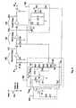
- FIG. 1is a block schematic of a preferred embodiment of the present invention
- FIG. 2is a detailed schematic of a preferred embodiment of the present invention.
- FIG. 3Ashows the characteristics of the V tss versus peak AC swing
- FIG. 3Bshows the output power P OUT , Gain, and efficiency characteristics of a temperature compensated power amplifier device constructed according to the principles of the present invention, and contrasted with uncompensated devices;
- FIG. 4is a characteristic of five devices in accordance with the present invention wherein the bias current I dq is shown as temperature varies between ⁇ 30° C. and +110° C.
- FIG. 1illustrates a linear power amplifier including the novel dynamic bias features of the present invention.
- the amplifierincludes a pre-amplifier stage 110 , a driver amplifier stage 120 , and an output amplifier stage 130 .
- the output of the driver amplifier stage 120is coupled to a driver output detector 140 .
- a bias adjustor circuit 150 in accordance with the present inventionis coupled to the driver ouptut detector 140 .
- the output of the bias adjustor circuit 150is coupled to the three-stage amplifier circuit via a coupling circuit comprising resistors R′ and R′′.
- resistors R′ and R′′are each 2K ⁇ .
- Temperature compensation circuit 160is coupled to the bias adjustor circuit 150 .
- Each of the three stages 110 , 120 , 130is preferably comprised of a depletion mode Gallium Arsenide (GaAs) Field Effect Transistor (FET) gain amplifier.
- GaAsGallium Arsenide
- FETField Effect Transistor
- the depletion mode FET current characteristicsare such that it draws maximum current (I dss ) when its gate-to-source voltage (V gs ) is zero, and minimum current (zero) when its gate-to-source voltage is negative Vp.
- the various modes of operationi.e., Class A, Class B and Class AB, are achieved by applying a suitable amount of gate-to-source voltage.
- the modes of operationcan be defined by the percentage of the maximum current drawn at each stage.
- the pre-amplifier stage 110is designed to operate in a Class A mode and primarily functions as a gain stage.
- the driver amplifier 120is configured to operate in a Class AB mode.
- the output amplifier 130is configured to operate in a Class AB mode or substantially close to a Class B mode.
- the driver output detector circuit 140comprises diode D 1 , resistor R 1 , capacitor C 1 , filter capacitor C 2 and resistive divider comprising resistors R 2 and R 3 .
- the dynamic bias adjustor circuit 150preferably comprises a pair of Field Effect Transistors (FET) Q 3 and Q 4 considered a reference Field Effect Transistor.
- Q 3is bias-coupled to the driver output detector circuit 140 .
- the drain of Q 3is preferably coupled to a current limiting resistor R o .
- the source of Q 3is coupled to ground. In an alternative embodiment, the source of Q 3 is coupled to ground via a resistor of suitable size.
- a source-follower circuitpreferably comprising FET Q 5 is coupled to both Q 3 and Q 4 (the reference FET).
- the source followeris provided with a reference voltage, V refB , applied at the gate of Q 5 .
- a plurality of diodes and resistorsform a level-shifting circuit 170 .
- four diodes D 2 , D 3 , D 4 , D 5 and resistor Rsform a level-shifting circuit 170 to produce a combined voltage level drop of about 2.6V.
- a FET Q 6with its gate and source tied together acts as a current source establishing the current through diodes D 2 , D 3 , D 4 and D 5 . It is operatively coupled to the level-shifting circuit 170 as shown.
- the temperature compensation circuit 160preferably comprises an FET Q 7 and a plurality of diodes connected to its gate. In a preferred embodiment, two diodes, D 6 and D 7 are used.
- One aspect of the present inventionis that a master-slave relationship is established between the driver stage 120 and the output stage 130 of the multi-stage power amplifier of FIG. 1 .
- the driver stage 120detects a need to generate a larger AC output voltage, it instructs itself and the other stages in the power amplifier to alter their operating modes from a deep Class AB or B mode to a Class AB mode.
- the multi-stage power amplifierdynamically adjusts its bias point to deliver optimum efficiency across a broad range of drive level conditions. It has been found that this approach additionally reduces the required idle (quiescent) current by about 60%. Further, this invention minimizes or extends the gain compression characteristics typically exhibited by fixed Class AB or Class B mode power amplifiers.
- the present inventioncontrols and stabilizes the bias point of a multi-stage power amplifier over a wide temperature range of ⁇ 30° C. to +110° C.
- the driver output detector circuit 140detects the alternating voltage (AC) signal swing at the driver output and generates a negative Direct Current (DC) voltage proportional to the peak AC swing V ac (i.e., the voltage range from peak-to-peak).
- the capacitor C 1filters out the fundamental frequency component of V ac and the resistive divider comprising resistors R 2 and R 3 determines the slope of the relationship between the peak AC voltage V ac and the DC output voltage (V tss ), as well as the maximum value that V tss can reach.
- FIG. 3Ashows the characteristics of the V tss versus peak AC power (P in ).
- V tssobtained at the driver output detector is applied to the gate of Q 3 .
- This gate voltagecontrols current I l through Resistor R o .
- Change in the current I lresults in a change in the voltage V refB applied at the source follower Q 5 .
- the output of the source follower Q 5is level-shifted by the level-shifting circuit 170 to the appropriate gate-to-source voltage V gs .
- V gsis used to set the operating mode of the three stages 110 , 120 and 130 of the power amplifier.
- V tssis also very small or zero.
- This voltage, V tssis applied to the gate of the transistor Q 3 .
- the drop in V refBforces the gate-to-source voltage, V gs , for all the stages, to become more negative, thereby making them draw less current.
- the driver's peak AC output voltage V acincreases.
- the driver output detector 140will begin to generate a negative voltage proportional to the peak AC output voltage.
- this voltagebecomes more and more negative and approaches the maximum level of DC voltage, which is determined by the resistor R 2 .
- the transistor Q 3draws less current, causing an increase in the voltage V refB .
- This increase in voltagein turn increases the voltage Vgs, thereby shifting the bias point of the amplifier stages toward a Class AB mode.
- a further feature of the circuit presented hereis temperature compensation circuit 160 .
- the plurality of diodes D 6 and D 7are configured to bias the transistor Q 7 close to pinch off (Vp), i.e., the point at which Q 7 permits current flow.
- Vppinch off
- a negative voltage, supplied by a series resistor Rref connected to Vssis also used to bias the transistor Q 7 .
- the operating point of transistor Q 7is similar to that of the output stage 130 of the amplifier.
- Diodes D 6 and D 7are selected such that they establish the required rate of change in the voltage drop across them versus temperature.
- Transistor Q 7 and resistor Rrefare selected such that the required slope in temperature compensation is achieved.
- FIG. 3Bshows the output power P OUT , Gain, and efficiency characteristics of a temperature-compensated power amplifier constructed according to the principles of the present invention.
- FIG. 4illustrates the variation of the bias current I dq versus temperature for five devices in accordance with the present invention, wherein the bias current I dq is shown as temperature varies between ⁇ 30° C. and +110° C. The figure illustrates that the amplifier's bias point can be controlled using the temperature compensation circuit described above. Also shown for comparison are plots for two uncompensated circuits in which the bias point changes linearly with temperature.
- a bias adjustment in accordance with the present inventioncan be achieved by detecting increases or decreases in distortion of the output signal (e.g., by comparing the input signal to the output signal).
- the instantaneous output AC swingcan be detected and the bias point can be dynamically adjusted in order to minimize gain compression (i.e., change from Class B mode to Class AB mode). This would result in reduced AM—AM distortion during the high instantaneous voltage peaks.
- the output AC voltage swingcan be detected to monitor substantial changes in output loading conditions. Variations in load conditions can result in substantial increases in peak output AC voltage swings that can be excessive and cause permanent damage to the output stage. These peak AC swings can be detected and an appropriate bias point change can be applied in order to either turn off the power amplifier or substantially reduce the overall power amplifier gain (i.e., change from Class AB mode to Class B mode).
Landscapes
- Engineering & Computer Science (AREA)
- Power Engineering (AREA)
- Amplifiers (AREA)
Abstract
Description
Claims (16)
Priority Applications (1)
| Application Number | Priority Date | Filing Date | Title |
|---|---|---|---|
| US10/208,636US6937102B2 (en) | 1999-08-10 | 2002-07-29 | Low bias current/temperature compensation current mirror for linear power amplifier |
Applications Claiming Priority (3)
| Application Number | Priority Date | Filing Date | Title |
|---|---|---|---|
| US14809999P | 1999-08-10 | 1999-08-10 | |
| US09/634,628US6559722B1 (en) | 1999-08-10 | 2000-08-08 | Low bias current/temperature compensation current mirror for linear power amplifier |
| US10/208,636US6937102B2 (en) | 1999-08-10 | 2002-07-29 | Low bias current/temperature compensation current mirror for linear power amplifier |
Related Parent Applications (1)
| Application Number | Title | Priority Date | Filing Date |
|---|---|---|---|
| US09/634,628ContinuationUS6559722B1 (en) | 1999-08-10 | 2000-08-08 | Low bias current/temperature compensation current mirror for linear power amplifier |
Publications (2)
| Publication Number | Publication Date |
|---|---|
| US20030006845A1 US20030006845A1 (en) | 2003-01-09 |
| US6937102B2true US6937102B2 (en) | 2005-08-30 |
Family
ID=26845516
Family Applications (2)
| Application Number | Title | Priority Date | Filing Date |
|---|---|---|---|
| US09/634,628Expired - LifetimeUS6559722B1 (en) | 1999-08-10 | 2000-08-08 | Low bias current/temperature compensation current mirror for linear power amplifier |
| US10/208,636Expired - LifetimeUS6937102B2 (en) | 1999-08-10 | 2002-07-29 | Low bias current/temperature compensation current mirror for linear power amplifier |
Family Applications Before (1)
| Application Number | Title | Priority Date | Filing Date |
|---|---|---|---|
| US09/634,628Expired - LifetimeUS6559722B1 (en) | 1999-08-10 | 2000-08-08 | Low bias current/temperature compensation current mirror for linear power amplifier |
Country Status (1)
| Country | Link |
|---|---|
| US (2) | US6559722B1 (en) |
Cited By (25)
| Publication number | Priority date | Publication date | Assignee | Title |
|---|---|---|---|---|
| US20040176053A1 (en)* | 2001-03-21 | 2004-09-09 | Kiichi Yamashita | Mobile telecommunication apparatus having a power amplifier which operates stably during changes in control voltage and temperature |
| US20050264361A1 (en)* | 2004-06-01 | 2005-12-01 | Vladimir Prodanov | Automatic biasing of a power device for linear operation |
| US20060099919A1 (en)* | 2004-10-22 | 2006-05-11 | Parkervision, Inc. | Systems and methods for vector power amplification |
| US20060290424A1 (en)* | 2005-06-28 | 2006-12-28 | Raul Salvi | Linear power efficient radio frequency (RF) driver system and method with power level control |
| US20070003291A1 (en)* | 2005-06-09 | 2007-01-04 | Kasper Bryon L | Distortion cancellation in a transimpedance amplifier circuit |
| US20070247217A1 (en)* | 2006-04-24 | 2007-10-25 | Sorrells David F | Systems and methods of rf power transmission, modulation, and amplification, including embodiments for amplifier class transitioning |
| US20080204145A1 (en)* | 2007-02-27 | 2008-08-28 | Gee Samuel Dow | Bias control circuit and method of controlling bias of rf power amplifier |
| US20080218270A1 (en)* | 2007-03-07 | 2008-09-11 | Gary Hau | Multi-mode power amplifier with low gain variation over temperature |
| US7620129B2 (en) | 2007-01-16 | 2009-11-17 | Parkervision, Inc. | RF power transmission, modulation, and amplification, including embodiments for generating vector modulation control signals |
| US20090298415A1 (en)* | 2008-06-02 | 2009-12-03 | Qualcomm Incorporated | Methods and apparatus for power reduction in a transceiver |
| US7885682B2 (en) | 2006-04-24 | 2011-02-08 | Parkervision, Inc. | Systems and methods of RF power transmission, modulation, and amplification, including architectural embodiments of same |
| US7911272B2 (en) | 2007-06-19 | 2011-03-22 | Parkervision, Inc. | Systems and methods of RF power transmission, modulation, and amplification, including blended control embodiments |
| US20110187459A1 (en)* | 2010-02-02 | 2011-08-04 | Mitsubishi Electric Corporation | Emitter-follower type bias circuit |
| US8013675B2 (en) | 2007-06-19 | 2011-09-06 | Parkervision, Inc. | Combiner-less multiple input single output (MISO) amplification with blended control |
| US8031804B2 (en) | 2006-04-24 | 2011-10-04 | Parkervision, Inc. | Systems and methods of RF tower transmission, modulation, and amplification, including embodiments for compensating for waveform distortion |
| US8315336B2 (en) | 2007-05-18 | 2012-11-20 | Parkervision, Inc. | Systems and methods of RF power transmission, modulation, and amplification, including a switching stage embodiment |
| US8319558B1 (en)* | 2008-10-14 | 2012-11-27 | Rf Micro Devices, Inc. | Bias-based linear high efficiency radio frequency amplifier |
| US8334722B2 (en) | 2007-06-28 | 2012-12-18 | Parkervision, Inc. | Systems and methods of RF power transmission, modulation and amplification |
| US8755454B2 (en) | 2011-06-02 | 2014-06-17 | Parkervision, Inc. | Antenna control |
| US9106316B2 (en) | 2005-10-24 | 2015-08-11 | Parkervision, Inc. | Systems and methods of RF power transmission, modulation, and amplification |
| US9438189B2 (en) | 2012-07-26 | 2016-09-06 | Qualcomm Incorporated | Low voltage multi-stage amplifier |
| US9608677B2 (en) | 2005-10-24 | 2017-03-28 | Parker Vision, Inc | Systems and methods of RF power transmission, modulation, and amplification |
| US9973180B2 (en) | 2015-12-30 | 2018-05-15 | Industrial Technology Research Institute | Output stage circuit |
| US10278131B2 (en) | 2013-09-17 | 2019-04-30 | Parkervision, Inc. | Method, apparatus and system for rendering an information bearing function of time |
| US11165392B2 (en) | 2018-08-01 | 2021-11-02 | Skyworks Solutions, Inc. | Variable power amplifier bias impedance |
Families Citing this family (61)
| Publication number | Priority date | Publication date | Assignee | Title |
|---|---|---|---|---|
| CN1302615C (en)* | 2000-08-28 | 2007-02-28 | 三菱电机株式会社 | Multistage amplifier |
| US6749335B2 (en)* | 2002-05-17 | 2004-06-15 | Sun Microsystems, Inc. | Adjustment and calibration system for post-fabrication treatment of on-chip temperature sensor |
| US6791418B2 (en)* | 2002-10-02 | 2004-09-14 | Koninklijke Philips Electronics N.V. | Capacitor coupled dynamic bias boosting circuit for a power amplifier |
| US20040072554A1 (en)* | 2002-10-15 | 2004-04-15 | Triquint Semiconductor, Inc. | Automatic-bias amplifier circuit |
| DE60313668T2 (en)* | 2002-12-16 | 2008-01-31 | Koninklijke Philips Electronics N.V. | SELF-ADAPTIVE VOLTAGE SWITCHING TO ENABLE DYNAMIC CONTROL OF CENTRAL HEAT IN A LINEAR POWER AMPLIFIER |
| US6831517B1 (en) | 2002-12-23 | 2004-12-14 | Intersil Americas, Inc. | Bias-management system and method for programmable RF power amplifier |
| US7145385B2 (en) | 2003-12-05 | 2006-12-05 | Telefonaktiebolaget Lm Ericsson (Publ) | Single chip power amplifier and envelope modulator |
| EP1719244B1 (en)* | 2004-02-17 | 2009-10-28 | TELEFONAKTIEBOLAGET LM ERICSSON (publ) | Dynamically biased amplifier |
| US6975172B2 (en)* | 2004-05-03 | 2005-12-13 | Peavey Electronics Corporation | Smart voltage rail reduction audio amplifier |
| WO2006079941A1 (en)* | 2005-01-25 | 2006-08-03 | Nxp B.V. | Synchronized temperature protection for class-ab amplifiers |
| US7276973B2 (en)* | 2005-06-29 | 2007-10-02 | Skyworks Solutions, Inc. | Automatic bias control circuit for linear power amplifiers |
| KR101411050B1 (en)* | 2006-04-24 | 2014-06-25 | 파커비전, 인크. | Systems and methods of rf power transmission, modulation, and amplification |
| US7890065B1 (en)* | 2006-09-01 | 2011-02-15 | Anadigics, Inc. | Temperature compensated power detector |
| TWI334689B (en)* | 2007-03-22 | 2010-12-11 | Novatek Microelectronics Corp | Dynamic biasing amplifier apparatus, dynamic biasing apparatus and method |
| GB0715254D0 (en) | 2007-08-03 | 2007-09-12 | Wolfson Ltd | Amplifier circuit |
| US7899416B2 (en)* | 2007-11-14 | 2011-03-01 | Crestcom, Inc. | RF transmitter with heat compensation and method therefor |
| US8854019B1 (en) | 2008-09-25 | 2014-10-07 | Rf Micro Devices, Inc. | Hybrid DC/DC power converter with charge-pump and buck converter |
| US9166471B1 (en) | 2009-03-13 | 2015-10-20 | Rf Micro Devices, Inc. | 3D frequency dithering for DC-to-DC converters used in multi-mode cellular transmitters |
| US8315576B2 (en) | 2009-05-05 | 2012-11-20 | Rf Micro Devices, Inc. | Capacitive compensation of cascaded directional couplers |
| US8548398B2 (en) | 2010-02-01 | 2013-10-01 | Rf Micro Devices, Inc. | Envelope power supply calibration of a multi-mode radio frequency power amplifier |
| US8538355B2 (en) | 2010-04-19 | 2013-09-17 | Rf Micro Devices, Inc. | Quadrature power amplifier architecture |
| US8989685B2 (en) | 2010-04-20 | 2015-03-24 | Rf Micro Devices, Inc. | Look-up table based configuration of multi-mode multi-band radio frequency power amplifier circuitry |
| US8542061B2 (en) | 2010-04-20 | 2013-09-24 | Rf Micro Devices, Inc. | Charge pump based power amplifier envelope power supply and bias power supply |
| US8947157B2 (en) | 2010-04-20 | 2015-02-03 | Rf Micro Devices, Inc. | Voltage multiplier charge pump buck |
| US8559898B2 (en) | 2010-04-20 | 2013-10-15 | Rf Micro Devices, Inc. | Embedded RF PA temperature compensating bias transistor |
| US8892063B2 (en) | 2010-04-20 | 2014-11-18 | Rf Micro Devices, Inc. | Linear mode and non-linear mode quadrature PA circuitry |
| US8712349B2 (en) | 2010-04-20 | 2014-04-29 | Rf Micro Devices, Inc. | Selecting a converter operating mode of a PA envelope power supply |
| US8706063B2 (en) | 2010-04-20 | 2014-04-22 | Rf Micro Devices, Inc. | PA envelope power supply undershoot compensation |
| US9553550B2 (en) | 2010-04-20 | 2017-01-24 | Qorvo Us, Inc. | Multiband RF switch ground isolation |
| US8831544B2 (en) | 2010-04-20 | 2014-09-09 | Rf Micro Devices, Inc. | Dynamic device switching (DDS) of an in-phase RF PA stage and a quadrature-phase RF PA stage |
| US9008597B2 (en) | 2010-04-20 | 2015-04-14 | Rf Micro Devices, Inc. | Direct current (DC)-DC converter having a multi-stage output filter |
| US8699973B2 (en) | 2010-04-20 | 2014-04-15 | Rf Micro Devices, Inc. | PA bias power supply efficiency optimization |
| US8731498B2 (en) | 2010-04-20 | 2014-05-20 | Rf Micro Devices, Inc. | Temperature correcting an envelope power supply signal for RF PA circuitry |
| US8958763B2 (en) | 2010-04-20 | 2015-02-17 | Rf Micro Devices, Inc. | PA bias power supply undershoot compensation |
| US8515361B2 (en) | 2010-04-20 | 2013-08-20 | Rf Micro Devices, Inc. | Frequency correction of a programmable frequency oscillator by propagation delay compensation |
| US9214865B2 (en) | 2010-04-20 | 2015-12-15 | Rf Micro Devices, Inc. | Voltage compatible charge pump buck and buck power supplies |
| US8942650B2 (en) | 2010-04-20 | 2015-01-27 | Rf Micro Devices, Inc. | RF PA linearity requirements based converter operating mode selection |
| US8571492B2 (en) | 2010-04-20 | 2013-10-29 | Rf Micro Devices, Inc. | DC-DC converter current sensing |
| US8913971B2 (en) | 2010-04-20 | 2014-12-16 | Rf Micro Devices, Inc. | Selecting PA bias levels of RF PA circuitry during a multislot burst |
| US8983407B2 (en)* | 2010-04-20 | 2015-03-17 | Rf Micro Devices, Inc. | Selectable PA bias temperature compensation circuitry |
| US8565694B2 (en) | 2010-04-20 | 2013-10-22 | Rf Micro Devices, Inc. | Split current current digital-to-analog converter (IDAC) for dynamic device switching (DDS) of an RF PA stage |
| US9362825B2 (en) | 2010-04-20 | 2016-06-07 | Rf Micro Devices, Inc. | Look-up table based configuration of a DC-DC converter |
| US9577590B2 (en) | 2010-04-20 | 2017-02-21 | Qorvo Us, Inc. | Dual inductive element charge pump buck and buck power supplies |
| US8811920B2 (en) | 2010-04-20 | 2014-08-19 | Rf Micro Devices, Inc. | DC-DC converter semiconductor die structure |
| US8942651B2 (en) | 2010-04-20 | 2015-01-27 | Rf Micro Devices, Inc. | Cascaded converged power amplifier |
| US9184701B2 (en) | 2010-04-20 | 2015-11-10 | Rf Micro Devices, Inc. | Snubber for a direct current (DC)-DC converter |
| US9030256B2 (en) | 2010-04-20 | 2015-05-12 | Rf Micro Devices, Inc. | Overlay class F choke |
| US9900204B2 (en) | 2010-04-20 | 2018-02-20 | Qorvo Us, Inc. | Multiple functional equivalence digital communications interface |
| US9214900B2 (en) | 2010-04-20 | 2015-12-15 | Rf Micro Devices, Inc. | Interference reduction between RF communications bands |
| US8983410B2 (en) | 2010-04-20 | 2015-03-17 | Rf Micro Devices, Inc. | Configurable 2-wire/3-wire serial communications interface |
| US8913967B2 (en) | 2010-04-20 | 2014-12-16 | Rf Micro Devices, Inc. | Feedback based buck timing of a direct current (DC)-DC converter |
| US9048787B2 (en) | 2010-04-20 | 2015-06-02 | Rf Micro Devices, Inc. | Combined RF detector and RF attenuator with concurrent outputs |
| US9077405B2 (en) | 2010-04-20 | 2015-07-07 | Rf Micro Devices, Inc. | High efficiency path based power amplifier circuitry |
| US8842399B2 (en) | 2010-04-20 | 2014-09-23 | Rf Micro Devices, Inc. | ESD protection of an RF PA semiconductor die using a PA controller semiconductor die |
| US8811921B2 (en) | 2010-04-20 | 2014-08-19 | Rf Micro Devices, Inc. | Independent PA biasing of a driver stage and a final stage |
| US9065505B2 (en) | 2012-01-31 | 2015-06-23 | Rf Micro Devices, Inc. | Optimal switching frequency for envelope tracking power supply |
| US9960740B2 (en)* | 2015-06-18 | 2018-05-01 | Raytheon Company | Bias circuitry for depletion mode amplifiers |
| US9634613B1 (en)* | 2016-03-18 | 2017-04-25 | Raytheon Company | Bias circuit having reduced power consumption |
| DE102017210759B4 (en)* | 2017-06-27 | 2019-04-18 | Fraunhofer-Gesellschaft zur Förderung der angewandten Forschung e.V. | Adaptive amplifier circuit to optimize the efficiency of a communication front-end |
| CN112803905B (en)* | 2021-04-14 | 2021-09-28 | 广州慧智微电子有限公司 | Compensation circuit |
| US20240235501A9 (en)* | 2022-10-20 | 2024-07-11 | Macom Technology Solutions Holdings, Inc. | Adaptive temperature peaking control for wideband amplifiers |
Citations (21)
| Publication number | Priority date | Publication date | Assignee | Title |
|---|---|---|---|---|
| US3984783A (en) | 1975-03-27 | 1976-10-05 | Motorola, Inc. | Amplifier |
| US4077013A (en) | 1976-06-04 | 1978-02-28 | Norlin Music, Incorporated | Audio power amplifier with automatic bias control |
| US4317083A (en) | 1979-03-19 | 1982-02-23 | Rca Corporation | Bias adjustment responsive to signal power |
| US4340867A (en) | 1980-11-05 | 1982-07-20 | Gte Laboratories Incorporated | Inverter amplifier |
| US4924194A (en) | 1989-05-19 | 1990-05-08 | Motorola, Inc. | RF power amplifier |
| US4956567A (en) | 1989-02-13 | 1990-09-11 | Texas Instruments Incorporated | Temperature compensated bias circuit |
| US5136257A (en) | 1988-12-08 | 1992-08-04 | Hewlett-Packard Company | RF amplifier bias circuit |
| US5311143A (en) | 1992-07-02 | 1994-05-10 | Motorola, Inc. | RF amplifier bias control method and apparatus |
| US5442321A (en) | 1993-07-08 | 1995-08-15 | Anadigics, Inc. | Automatic transimpedance control amplifier |
| US5646573A (en) | 1995-02-28 | 1997-07-08 | Anadigics, Inc. | Automatic gain-control transimpedence amplifier |
| US5757236A (en) | 1996-07-01 | 1998-05-26 | Motorola, Inc. | Amplifier bias circuit and method |
| US5774017A (en) | 1996-06-03 | 1998-06-30 | Anadigics, Inc. | Multiple-band amplifier |
| US5892400A (en) | 1995-12-15 | 1999-04-06 | Anadigics, Inc. | Amplifier using a single polarity power supply and including depletion mode FET and negative voltage generator |
| US5923215A (en) | 1996-06-13 | 1999-07-13 | The Whitaker Corporation | Linearized amplifier |
| US5942946A (en) | 1997-10-10 | 1999-08-24 | Industrial Technology Research Institute | RF power amplifier with high efficiency and a wide range of gain control |
| US5982236A (en) | 1997-01-21 | 1999-11-09 | Matsushita Electric Industrial Co., Ltd. | High-frequency power amplifier |
| US6020787A (en)* | 1995-06-07 | 2000-02-01 | Motorola, Inc. | Method and apparatus for amplifying a signal |
| US6194968B1 (en) | 1999-05-10 | 2001-02-27 | Tyco Electronics Logistics Ag | Temperature and process compensating circuit and controller for an RF power amplifier |
| US6201440B1 (en)* | 1998-06-23 | 2001-03-13 | Nec Corporation | Power amplifier and control circuit thereof |
| US6204731B1 (en) | 1998-12-05 | 2001-03-20 | Institute Of Microelectronics | Power amplifier |
| US6314008B1 (en) | 2000-10-16 | 2001-11-06 | Jianwen Bao | Adjustable low spurious signal DC-DC converter |
Family Cites Families (1)
| Publication number | Priority date | Publication date | Assignee | Title |
|---|---|---|---|---|
| JPH06334541A (en)* | 1993-05-25 | 1994-12-02 | Sony Corp | Radio transmitter |
- 2000
- 2000-08-08USUS09/634,628patent/US6559722B1/ennot_activeExpired - Lifetime
- 2002
- 2002-07-29USUS10/208,636patent/US6937102B2/ennot_activeExpired - Lifetime
Patent Citations (25)
| Publication number | Priority date | Publication date | Assignee | Title |
|---|---|---|---|---|
| US3984783A (en) | 1975-03-27 | 1976-10-05 | Motorola, Inc. | Amplifier |
| US4077013A (en) | 1976-06-04 | 1978-02-28 | Norlin Music, Incorporated | Audio power amplifier with automatic bias control |
| US4317083A (en) | 1979-03-19 | 1982-02-23 | Rca Corporation | Bias adjustment responsive to signal power |
| US4340867A (en) | 1980-11-05 | 1982-07-20 | Gte Laboratories Incorporated | Inverter amplifier |
| US5136257A (en) | 1988-12-08 | 1992-08-04 | Hewlett-Packard Company | RF amplifier bias circuit |
| US4956567A (en) | 1989-02-13 | 1990-09-11 | Texas Instruments Incorporated | Temperature compensated bias circuit |
| US4924194A (en) | 1989-05-19 | 1990-05-08 | Motorola, Inc. | RF power amplifier |
| US5311143A (en) | 1992-07-02 | 1994-05-10 | Motorola, Inc. | RF amplifier bias control method and apparatus |
| US5442321A (en) | 1993-07-08 | 1995-08-15 | Anadigics, Inc. | Automatic transimpedance control amplifier |
| US5602510A (en) | 1993-07-08 | 1997-02-11 | Anadigics, Inc. | Automatic transimpedance control amplifier having a variable impedance feedback |
| US5646573A (en) | 1995-02-28 | 1997-07-08 | Anadigics, Inc. | Automatic gain-control transimpedence amplifier |
| US6020787A (en)* | 1995-06-07 | 2000-02-01 | Motorola, Inc. | Method and apparatus for amplifying a signal |
| US5892400A (en) | 1995-12-15 | 1999-04-06 | Anadigics, Inc. | Amplifier using a single polarity power supply and including depletion mode FET and negative voltage generator |
| US5952860A (en) | 1995-12-15 | 1999-09-14 | Anadigics, Inc. | Amplifier using a single polarity power supply |
| US6242986B1 (en) | 1996-06-03 | 2001-06-05 | Anadigics, Inc. | Multiple-band amplifier |
| US5774017A (en) | 1996-06-03 | 1998-06-30 | Anadigics, Inc. | Multiple-band amplifier |
| US20010011926A1 (en) | 1996-06-03 | 2001-08-09 | Anadigics, Inc. | Multiple-band amplifier |
| US5923215A (en) | 1996-06-13 | 1999-07-13 | The Whitaker Corporation | Linearized amplifier |
| US5757236A (en) | 1996-07-01 | 1998-05-26 | Motorola, Inc. | Amplifier bias circuit and method |
| US5982236A (en) | 1997-01-21 | 1999-11-09 | Matsushita Electric Industrial Co., Ltd. | High-frequency power amplifier |
| US5942946A (en) | 1997-10-10 | 1999-08-24 | Industrial Technology Research Institute | RF power amplifier with high efficiency and a wide range of gain control |
| US6201440B1 (en)* | 1998-06-23 | 2001-03-13 | Nec Corporation | Power amplifier and control circuit thereof |
| US6204731B1 (en) | 1998-12-05 | 2001-03-20 | Institute Of Microelectronics | Power amplifier |
| US6194968B1 (en) | 1999-05-10 | 2001-02-27 | Tyco Electronics Logistics Ag | Temperature and process compensating circuit and controller for an RF power amplifier |
| US6314008B1 (en) | 2000-10-16 | 2001-11-06 | Jianwen Bao | Adjustable low spurious signal DC-DC converter |
Non-Patent Citations (3)
| Title |
|---|
| Sato et al., "Intelligent RF Power Module Using Automatic Bias Control (ABC) System for PCS CDMA Application" IEEE MTT-S International Microwave Symposium Digest, Jun. 1998. |
| U.S. Appl. No. 09/668,181, filed Sep. 22, 2000, van Saders et al. |
| U.S. Appl. No. 09/875,117, filed Jun. 6, 2001, Liwinski. |
Cited By (85)
| Publication number | Priority date | Publication date | Assignee | Title |
|---|---|---|---|---|
| US20040176053A1 (en)* | 2001-03-21 | 2004-09-09 | Kiichi Yamashita | Mobile telecommunication apparatus having a power amplifier which operates stably during changes in control voltage and temperature |
| US7084705B2 (en)* | 2004-06-01 | 2006-08-01 | Agere Systems Inc. | Automatic biasing of a power device for linear operation |
| US20050264361A1 (en)* | 2004-06-01 | 2005-12-01 | Vladimir Prodanov | Automatic biasing of a power device for linear operation |
| US8280321B2 (en) | 2004-10-22 | 2012-10-02 | Parkervision, Inc. | Systems and methods of RF power transmission, modulation, and amplification, including Cartesian-Polar-Cartesian-Polar (CPCP) embodiments |
| US9197164B2 (en) | 2004-10-22 | 2015-11-24 | Parkervision, Inc. | RF power transmission, modulation, and amplification, including direct cartesian 2-branch embodiments |
| US8639196B2 (en) | 2004-10-22 | 2014-01-28 | Parkervision, Inc. | Control modules |
| US7184723B2 (en) | 2004-10-22 | 2007-02-27 | Parkervision, Inc. | Systems and methods for vector power amplification |
| US8626093B2 (en) | 2004-10-22 | 2014-01-07 | Parkervision, Inc. | RF power transmission, modulation, and amplification embodiments |
| US8577313B2 (en) | 2004-10-22 | 2013-11-05 | Parkervision, Inc. | Systems and methods of RF power transmission, modulation, and amplification, including output stage protection circuitry |
| US7327803B2 (en) | 2004-10-22 | 2008-02-05 | Parkervision, Inc. | Systems and methods for vector power amplification |
| US8913974B2 (en) | 2004-10-22 | 2014-12-16 | Parkervision, Inc. | RF power transmission, modulation, and amplification, including direct cartesian 2-branch embodiments |
| US8447248B2 (en) | 2004-10-22 | 2013-05-21 | Parkervision, Inc. | RF power transmission, modulation, and amplification, including power control of multiple input single output (MISO) amplifiers |
| US8433264B2 (en) | 2004-10-22 | 2013-04-30 | Parkervision, Inc. | Multiple input single output (MISO) amplifier having multiple transistors whose output voltages substantially equal the amplifier output voltage |
| US8428527B2 (en) | 2004-10-22 | 2013-04-23 | Parkervision, Inc. | RF power transmission, modulation, and amplification, including direct cartesian 2-branch embodiments |
| US7421036B2 (en) | 2004-10-22 | 2008-09-02 | Parkervision, Inc. | Systems and methods of RF power transmission, modulation, and amplification, including transfer function embodiments |
| US8406711B2 (en) | 2004-10-22 | 2013-03-26 | Parkervision, Inc. | Systems and methods of RF power transmission, modulation, and amplification, including a Cartesian-Polar-Cartesian-Polar (CPCP) embodiment |
| US9768733B2 (en) | 2004-10-22 | 2017-09-19 | Parker Vision, Inc. | Multiple input single output device with vector signal and bias signal inputs |
| US8351870B2 (en) | 2004-10-22 | 2013-01-08 | Parkervision, Inc. | Systems and methods of RF power transmission, modulation, and amplification, including cartesian 4-branch embodiments |
| US7466760B2 (en) | 2004-10-22 | 2008-12-16 | Parkervision, Inc. | Systems and methods of RF power transmission, modulation, and amplification, including transfer function embodiments |
| US7526261B2 (en) | 2004-10-22 | 2009-04-28 | Parkervision, Inc. | RF power transmission, modulation, and amplification, including cartesian 4-branch embodiments |
| US20060099919A1 (en)* | 2004-10-22 | 2006-05-11 | Parkervision, Inc. | Systems and methods for vector power amplification |
| US9143088B2 (en) | 2004-10-22 | 2015-09-22 | Parkervision, Inc. | Control modules |
| US9166528B2 (en) | 2004-10-22 | 2015-10-20 | Parkervision, Inc. | RF power transmission, modulation, and amplification embodiments |
| US7639072B2 (en) | 2004-10-22 | 2009-12-29 | Parkervision, Inc. | Controlling a power amplifier to transition among amplifier operational classes according to at least an output signal waveform trajectory |
| US7647030B2 (en) | 2004-10-22 | 2010-01-12 | Parkervision, Inc. | Multiple input single output (MISO) amplifier with circuit branch output tracking |
| US7672650B2 (en) | 2004-10-22 | 2010-03-02 | Parkervision, Inc. | Systems and methods of RF power transmission, modulation, and amplification, including multiple input single output (MISO) amplifier embodiments comprising harmonic control circuitry |
| US8781418B2 (en) | 2004-10-22 | 2014-07-15 | Parkervision, Inc. | Power amplification based on phase angle controlled reference signal and amplitude control signal |
| US7835709B2 (en) | 2004-10-22 | 2010-11-16 | Parkervision, Inc. | RF power transmission, modulation, and amplification using multiple input single output (MISO) amplifiers to process phase angle and magnitude information |
| US7844235B2 (en) | 2004-10-22 | 2010-11-30 | Parkervision, Inc. | RF power transmission, modulation, and amplification, including harmonic control embodiments |
| US8233858B2 (en) | 2004-10-22 | 2012-07-31 | Parkervision, Inc. | RF power transmission, modulation, and amplification embodiments, including control circuitry for controlling power amplifier output stages |
| US7932776B2 (en) | 2004-10-22 | 2011-04-26 | Parkervision, Inc. | RF power transmission, modulation, and amplification embodiments |
| US7945224B2 (en) | 2004-10-22 | 2011-05-17 | Parkervision, Inc. | Systems and methods of RF power transmission, modulation, and amplification, including waveform distortion compensation embodiments |
| US9197163B2 (en) | 2004-10-22 | 2015-11-24 | Parkvision, Inc. | Systems, and methods of RF power transmission, modulation, and amplification, including embodiments for output stage protection |
| US20070003291A1 (en)* | 2005-06-09 | 2007-01-04 | Kasper Bryon L | Distortion cancellation in a transimpedance amplifier circuit |
| US20060290424A1 (en)* | 2005-06-28 | 2006-12-28 | Raul Salvi | Linear power efficient radio frequency (RF) driver system and method with power level control |
| US7250817B2 (en)* | 2005-06-28 | 2007-07-31 | Motorola, Inc. | Linear power efficient radio frequency (RF) driver system and method with power level control |
| US9614484B2 (en) | 2005-10-24 | 2017-04-04 | Parkervision, Inc. | Systems and methods of RF power transmission, modulation, and amplification, including control functions to transition an output of a MISO device |
| US9094085B2 (en) | 2005-10-24 | 2015-07-28 | Parkervision, Inc. | Control of MISO node |
| US9608677B2 (en) | 2005-10-24 | 2017-03-28 | Parker Vision, Inc | Systems and methods of RF power transmission, modulation, and amplification |
| US9419692B2 (en) | 2005-10-24 | 2016-08-16 | Parkervision, Inc. | Antenna control |
| US9106316B2 (en) | 2005-10-24 | 2015-08-11 | Parkervision, Inc. | Systems and methods of RF power transmission, modulation, and amplification |
| US9705540B2 (en) | 2005-10-24 | 2017-07-11 | Parker Vision, Inc. | Control of MISO node |
| US7750733B2 (en) | 2006-04-24 | 2010-07-06 | Parkervision, Inc. | Systems and methods of RF power transmission, modulation, and amplification, including embodiments for extending RF transmission bandwidth |
| US9106500B2 (en) | 2006-04-24 | 2015-08-11 | Parkervision, Inc. | Systems and methods of RF power transmission, modulation, and amplification, including embodiments for error correction |
| US7885682B2 (en) | 2006-04-24 | 2011-02-08 | Parkervision, Inc. | Systems and methods of RF power transmission, modulation, and amplification, including architectural embodiments of same |
| US20070247217A1 (en)* | 2006-04-24 | 2007-10-25 | Sorrells David F | Systems and methods of rf power transmission, modulation, and amplification, including embodiments for amplifier class transitioning |
| US7929989B2 (en) | 2006-04-24 | 2011-04-19 | Parkervision, Inc. | Systems and methods of RF power transmission, modulation, and amplification, including architectural embodiments of same |
| US8050353B2 (en) | 2006-04-24 | 2011-11-01 | Parkervision, Inc. | Systems and methods of RF power transmission, modulation, and amplification, including embodiments for compensating for waveform distortion |
| US7378902B2 (en) | 2006-04-24 | 2008-05-27 | Parkervision, Inc | Systems and methods of RF power transmission, modulation, and amplification, including embodiments for gain and phase control |
| US8036306B2 (en) | 2006-04-24 | 2011-10-11 | Parkervision, Inc. | Systems and methods of RF power transmission, modulation and amplification, including embodiments for compensating for waveform distortion |
| US7423477B2 (en) | 2006-04-24 | 2008-09-09 | Parkervision, Inc. | Systems and methods of RF power transmission, modulation, and amplification, including embodiments for amplifier class transitioning |
| US8059749B2 (en) | 2006-04-24 | 2011-11-15 | Parkervision, Inc. | Systems and methods of RF power transmission, modulation, and amplification, including embodiments for compensating for waveform distortion |
| US8031804B2 (en) | 2006-04-24 | 2011-10-04 | Parkervision, Inc. | Systems and methods of RF tower transmission, modulation, and amplification, including embodiments for compensating for waveform distortion |
| US7414469B2 (en) | 2006-04-24 | 2008-08-19 | Parkervision, Inc. | Systems and methods of RF power transmission, modulation, and amplification, including embodiments for amplifier class transitioning |
| US7937106B2 (en) | 2006-04-24 | 2011-05-03 | ParkerVision, Inc, | Systems and methods of RF power transmission, modulation, and amplification, including architectural embodiments of same |
| US8026764B2 (en) | 2006-04-24 | 2011-09-27 | Parkervision, Inc. | Generation and amplification of substantially constant envelope signals, including switching an output among a plurality of nodes |
| US7949365B2 (en) | 2006-04-24 | 2011-05-24 | Parkervision, Inc. | Systems and methods of RF power transmission, modulation, and amplification, including architectural embodiments of same |
| US7355470B2 (en) | 2006-04-24 | 2008-04-08 | Parkervision, Inc. | Systems and methods of RF power transmission, modulation, and amplification, including embodiments for amplifier class transitioning |
| US8913691B2 (en) | 2006-08-24 | 2014-12-16 | Parkervision, Inc. | Controlling output power of multiple-input single-output (MISO) device |
| US7620129B2 (en) | 2007-01-16 | 2009-11-17 | Parkervision, Inc. | RF power transmission, modulation, and amplification, including embodiments for generating vector modulation control signals |
| US7439806B2 (en)* | 2007-02-27 | 2008-10-21 | Avago Technologies General Ip (Singapore) Pte. Ltd. | Bias control circuit and method of controlling bias of RF power amplifier |
| US20080204145A1 (en)* | 2007-02-27 | 2008-08-28 | Gee Samuel Dow | Bias control circuit and method of controlling bias of rf power amplifier |
| US7554407B2 (en) | 2007-03-07 | 2009-06-30 | Fairchild Semiconductor Corporation | Multi-mode power amplifier with low gain variation over temperature |
| US20080218270A1 (en)* | 2007-03-07 | 2008-09-11 | Gary Hau | Multi-mode power amplifier with low gain variation over temperature |
| US8548093B2 (en) | 2007-05-18 | 2013-10-01 | Parkervision, Inc. | Power amplification based on frequency control signal |
| US8315336B2 (en) | 2007-05-18 | 2012-11-20 | Parkervision, Inc. | Systems and methods of RF power transmission, modulation, and amplification, including a switching stage embodiment |
| US8502600B2 (en) | 2007-06-19 | 2013-08-06 | Parkervision, Inc. | Combiner-less multiple input single output (MISO) amplification with blended control |
| US8013675B2 (en) | 2007-06-19 | 2011-09-06 | Parkervision, Inc. | Combiner-less multiple input single output (MISO) amplification with blended control |
| US8766717B2 (en) | 2007-06-19 | 2014-07-01 | Parkervision, Inc. | Systems and methods of RF power transmission, modulation, and amplification, including varying weights of control signals |
| US8461924B2 (en) | 2007-06-19 | 2013-06-11 | Parkervision, Inc. | Systems and methods of RF power transmission, modulation, and amplification, including embodiments for controlling a transimpedance node |
| US8410849B2 (en) | 2007-06-19 | 2013-04-02 | Parkervision, Inc. | Systems and methods of RF power transmission, modulation, and amplification, including blended control embodiments |
| US7911272B2 (en) | 2007-06-19 | 2011-03-22 | Parkervision, Inc. | Systems and methods of RF power transmission, modulation, and amplification, including blended control embodiments |
| US8334722B2 (en) | 2007-06-28 | 2012-12-18 | Parkervision, Inc. | Systems and methods of RF power transmission, modulation and amplification |
| US8884694B2 (en) | 2007-06-28 | 2014-11-11 | Parkervision, Inc. | Systems and methods of RF power transmission, modulation, and amplification |
| US8565669B2 (en) | 2008-06-02 | 2013-10-22 | Qualcomm, Incorporated | Methods and apparatus for power reduction in a transceiver |
| US20090298415A1 (en)* | 2008-06-02 | 2009-12-03 | Qualcomm Incorporated | Methods and apparatus for power reduction in a transceiver |
| US8319558B1 (en)* | 2008-10-14 | 2012-11-27 | Rf Micro Devices, Inc. | Bias-based linear high efficiency radio frequency amplifier |
| US8138836B2 (en)* | 2010-02-02 | 2012-03-20 | Mitsubishi Electric Corporation | Emitter-follower type bias circuit |
| US20110187459A1 (en)* | 2010-02-02 | 2011-08-04 | Mitsubishi Electric Corporation | Emitter-follower type bias circuit |
| US8755454B2 (en) | 2011-06-02 | 2014-06-17 | Parkervision, Inc. | Antenna control |
| US9438189B2 (en) | 2012-07-26 | 2016-09-06 | Qualcomm Incorporated | Low voltage multi-stage amplifier |
| US10278131B2 (en) | 2013-09-17 | 2019-04-30 | Parkervision, Inc. | Method, apparatus and system for rendering an information bearing function of time |
| US9973180B2 (en) | 2015-12-30 | 2018-05-15 | Industrial Technology Research Institute | Output stage circuit |
| US11165392B2 (en) | 2018-08-01 | 2021-11-02 | Skyworks Solutions, Inc. | Variable power amplifier bias impedance |
| US11894808B2 (en) | 2018-08-01 | 2024-02-06 | Skyworks Solutions, Inc. | Power amplifier with variable bias impedance |
Also Published As
| Publication number | Publication date |
|---|---|
| US6559722B1 (en) | 2003-05-06 |
| US20030006845A1 (en) | 2003-01-09 |
Similar Documents
| Publication | Publication Date | Title |
|---|---|---|
| US6937102B2 (en) | Low bias current/temperature compensation current mirror for linear power amplifier | |
| KR101124914B1 (en) | System and method for current-mode amplitude modulation | |
| US7928799B2 (en) | Power amplifying apparatus and mobile communication terminal | |
| US11929721B2 (en) | Power amplifier module | |
| US6404284B1 (en) | Amplifier bias adjustment circuit to maintain high-output third-order intermodulation distortion performance | |
| US6313705B1 (en) | Bias network for high efficiency RF linear power amplifier | |
| US7288987B2 (en) | RF amplifier employing active load linearization | |
| US7295064B2 (en) | Doherty amplifier | |
| US7102427B2 (en) | Amplifier and radio frequency power amplifier using the same | |
| US7728662B2 (en) | Saturated power amplifier with selectable and variable output power levels | |
| US6236266B1 (en) | Bias circuit and bias supply method for a multistage power amplifier | |
| US7649413B2 (en) | High-frequency power amplifier improved in size and cost | |
| US9350300B2 (en) | Power amplifier | |
| US20060244523A1 (en) | Power control and modulation of switched-mode power amplifiers with one or more stages | |
| US7218175B1 (en) | Dynamic feedback linearization | |
| US6819180B2 (en) | Radio frequency power amplifier adaptive bias control circuit | |
| US7288992B2 (en) | Bias circuit for a bipolar transistor | |
| EP1469592B1 (en) | Apparatus for and method of controlling the base bias voltage of an HBT | |
| US7265627B2 (en) | Self adaptable bias circuit for enabling dynamic control of quiescent current in a linear power amplifier | |
| US20040095192A1 (en) | Radio frequency power amplifier adaptive bias control circuit | |
| JPH11220338A (en) | High frequency power amplifier | |
| US6600344B1 (en) | Predistortion circuit for RF detector | |
| KR20230117527A (en) | Power amplifier using multi-path common-mode feedback loop | |
| CN114584077A (en) | Bias circuit of Doherty power amplifier | |
| US6107872A (en) | Adaptive control of RF power amplifier power supply voltage |
Legal Events
| Date | Code | Title | Description |
|---|---|---|---|
| STCF | Information on status: patent grant | Free format text:PATENTED CASE | |
| CC | Certificate of correction | ||
| FPAY | Fee payment | Year of fee payment:4 | |
| FPAY | Fee payment | Year of fee payment:8 | |
| AS | Assignment | Owner name:ANADIGICS, INC., NEW JERSEY Free format text:ASSIGNMENT OF ASSIGNORS INTEREST;ASSIGNORS:LOPEZ, OSVALDO J.;BAYRUNS, ROBERT;SINGH, MAHENDRA;SIGNING DATES FROM 20001205 TO 20010827;REEL/FRAME:033987/0750 | |
| AS | Assignment | Owner name:SILICON VALLEY BANK, MASSACHUSETTS Free format text:SECURITY AGREEMENT;ASSIGNOR:ANADIGICS, INC.;REEL/FRAME:034056/0641 Effective date:20141024 | |
| AS | Assignment | Owner name:II-IV INCORPORATED, PENNSYLVANIA Free format text:INTELLECTUAL PROPERTY SECURITY AGREEMENT;ASSIGNOR:ANADIGICS, INC.;REEL/FRAME:037973/0226 Effective date:20160226 Owner name:ANADIGICS, INC., NEW JERSEY Free format text:RELEASE BY SECURED PARTY;ASSIGNOR:SILICON VALLEY BANK;REEL/FRAME:037973/0133 Effective date:20160301 | |
| AS | Assignment | Owner name:ANADIGICS, INC., NEW JERSEY Free format text:RELEASE BY SECURED PARTY;ASSIGNOR:II-VI INCORPORATED;REEL/FRAME:038119/0312 Effective date:20160315 | |
| AS | Assignment | Owner name:II-VI INCORPORATED, PENNSYLVANIA Free format text:CORRECTIVE ASSIGNMENT TO CORRECT THE ASSIGNEE'S NAME PREVIOUSLY RECORDED AT REEL: 037973 FRAME: 0226. ASSIGNOR(S) HEREBY CONFIRMS THE SECURITY AGREEMENT;ASSIGNOR:ANADIGICS, INC.;REEL/FRAME:038744/0835 Effective date:20160226 | |
| AS | Assignment | Owner name:SILICON VALLEY BANK, MASSACHUSETTS Free format text:CORRECTIVE ASSIGNMENT TO CORRECT THE ERRONEOUS NUMBER 6790900 AND REPLACE IT WITH 6760900 PREVIOUSLY RECORDED ON REEL 034056 FRAME 0641. ASSIGNOR(S) HEREBY CONFIRMS THE SECURITY AGREEMENT;ASSIGNOR:ANADIGICS, INC.;REEL/FRAME:040660/0967 Effective date:20141024 | |
| FPAY | Fee payment | Year of fee payment:12 | |
| AS | Assignment | Owner name:II-VI OPTOELECTRONIC DEVICES, INC., NEW JERSEY Free format text:CHANGE OF NAME;ASSIGNOR:ANADIGICS, INC.;REEL/FRAME:042381/0761 Effective date:20160729 | |
| AS | Assignment | Owner name:SKYWORKS SOLUTIONS, INC., MASSACHUSETTS Free format text:ASSIGNMENT OF ASSIGNORS INTEREST;ASSIGNOR:II-VI OPTOELECTRONIC DEVICES, INC.;REEL/FRAME:042551/0708 Effective date:20170308 |