US6936860B2 - Light emitting diode having an insulating substrate - Google Patents
Light emitting diode having an insulating substrateDownload PDFInfo
- Publication number
- US6936860B2 US6936860B2US10/063,822US6382202AUS6936860B2US 6936860 B2US6936860 B2US 6936860B2US 6382202 AUS6382202 AUS 6382202AUS 6936860 B2US6936860 B2US 6936860B2
- Authority
- US
- United States
- Prior art keywords
- type
- layer
- ohmic contact
- contact electrode
- insulating substrate
- Prior art date
- Legal status (The legal status is an assumption and is not a legal conclusion. Google has not performed a legal analysis and makes no representation as to the accuracy of the status listed.)
- Expired - Lifetime
Links
- 239000000758substrateSubstances0.000titleclaimsabstractdescription33
- 238000005253claddingMethods0.000claimsabstractdescription23
- 239000000463materialSubstances0.000claimsabstractdescription9
- JMASRVWKEDWRBT-UHFFFAOYSA-NGallium nitrideChemical compound[Ga]#NJMASRVWKEDWRBT-UHFFFAOYSA-N0.000claimsdescription11
- 229910052594sapphireInorganic materials0.000claimsdescription5
- 239000010980sapphireSubstances0.000claimsdescription5
- 239000004065semiconductorSubstances0.000claims12
- 229910052755nonmetalInorganic materials0.000claims7
- BEQNOZDXPONEMR-UHFFFAOYSA-Ncadmium;oxotinChemical compound[Cd].[Sn]=OBEQNOZDXPONEMR-UHFFFAOYSA-N0.000claims4
- AMGQUBHHOARCQH-UHFFFAOYSA-Nindium;oxotinChemical compound[In].[Sn]=OAMGQUBHHOARCQH-UHFFFAOYSA-N0.000claims4
- 239000007769metal materialSubstances0.000claims1
- 229910002601GaNInorganic materials0.000description6
- 238000000034methodMethods0.000description5
- 238000004519manufacturing processMethods0.000description3
- 229910002704AlGaNInorganic materials0.000description2
- PXHVJJICTQNCMI-UHFFFAOYSA-NNickelChemical compound[Ni]PXHVJJICTQNCMI-UHFFFAOYSA-N0.000description2
- 238000010586diagramMethods0.000description2
- 230000008020evaporationEffects0.000description2
- 238000001704evaporationMethods0.000description2
- 230000005641tunnelingEffects0.000description2
- 229910000838Al alloyInorganic materials0.000description1
- 229910001020Au alloyInorganic materials0.000description1
- RTAQQCXQSZGOHL-UHFFFAOYSA-NTitaniumChemical compound[Ti]RTAQQCXQSZGOHL-UHFFFAOYSA-N0.000description1
- 230000004075alterationEffects0.000description1
- UQZIWOQVLUASCR-UHFFFAOYSA-Nalumane;titaniumChemical compound[AlH3].[Ti]UQZIWOQVLUASCR-UHFFFAOYSA-N0.000description1
- 229910052782aluminiumInorganic materials0.000description1
- XAGFODPZIPBFFR-UHFFFAOYSA-NaluminiumChemical compound[Al]XAGFODPZIPBFFR-UHFFFAOYSA-N0.000description1
- 238000004891communicationMethods0.000description1
- 238000013500data storageMethods0.000description1
- 230000000694effectsEffects0.000description1
- PCHJSUWPFVWCPO-UHFFFAOYSA-NgoldChemical compound[Au]PCHJSUWPFVWCPO-UHFFFAOYSA-N0.000description1
- 229910052737goldInorganic materials0.000description1
- 239000010931goldSubstances0.000description1
- 239000003353gold alloySubstances0.000description1
- MSNOMDLPLDYDME-UHFFFAOYSA-Ngold nickelChemical compound[Ni].[Au]MSNOMDLPLDYDME-UHFFFAOYSA-N0.000description1
- 238000005286illuminationMethods0.000description1
- 238000012986modificationMethods0.000description1
- 230000004048modificationEffects0.000description1
- 229910052759nickelInorganic materials0.000description1
- 230000003287optical effectEffects0.000description1
- 239000010936titaniumSubstances0.000description1
- 229910052719titaniumInorganic materials0.000description1
Images

Classifications
- H—ELECTRICITY
- H10—SEMICONDUCTOR DEVICES; ELECTRIC SOLID-STATE DEVICES NOT OTHERWISE PROVIDED FOR
- H10H—INORGANIC LIGHT-EMITTING SEMICONDUCTOR DEVICES HAVING POTENTIAL BARRIERS
- H10H20/00—Individual inorganic light-emitting semiconductor devices having potential barriers, e.g. light-emitting diodes [LED]
- H10H20/80—Constructional details
- H10H20/81—Bodies
- H10H20/811—Bodies having quantum effect structures or superlattices, e.g. tunnel junctions
- H—ELECTRICITY
- H10—SEMICONDUCTOR DEVICES; ELECTRIC SOLID-STATE DEVICES NOT OTHERWISE PROVIDED FOR
- H10H—INORGANIC LIGHT-EMITTING SEMICONDUCTOR DEVICES HAVING POTENTIAL BARRIERS
- H10H20/00—Individual inorganic light-emitting semiconductor devices having potential barriers, e.g. light-emitting diodes [LED]
- H10H20/80—Constructional details
- H10H20/81—Bodies
- H10H20/816—Bodies having carrier transport control structures, e.g. highly-doped semiconductor layers or current-blocking structures
- H—ELECTRICITY
- H10—SEMICONDUCTOR DEVICES; ELECTRIC SOLID-STATE DEVICES NOT OTHERWISE PROVIDED FOR
- H10H—INORGANIC LIGHT-EMITTING SEMICONDUCTOR DEVICES HAVING POTENTIAL BARRIERS
- H10H20/00—Individual inorganic light-emitting semiconductor devices having potential barriers, e.g. light-emitting diodes [LED]
- H10H20/80—Constructional details
- H10H20/81—Bodies
- H10H20/822—Materials of the light-emitting regions
- H10H20/824—Materials of the light-emitting regions comprising only Group III-V materials, e.g. GaP
- H10H20/825—Materials of the light-emitting regions comprising only Group III-V materials, e.g. GaP containing nitrogen, e.g. GaN
- H10H20/8252—Materials of the light-emitting regions comprising only Group III-V materials, e.g. GaP containing nitrogen, e.g. GaN characterised by the dopants
Definitions
- the present inventionrelates to a light emitting diode (LED), and more particularly, to a light emitting diode having an insulating substrate.
- LEDlight emitting diode
- LEDsLight emitting diodes
- optical display devicesincluding optical display devices, traffic lights, data storage equipment, communication devices, illumination apparatuses, and medical treatment equipment.
- One of the main goals of engineers who design LEDsis to increase the brightness of the light emitted from LEDs.
- U.S. Pat. No. 5,563,422discloses a gallium nitride (GaN)-based LED in FIG. 10.
- the LEDhas a p-type ohmic contact electrode 56 made of nickel, gold or a nickel-gold alloy.
- the LEDalso has an n-type ohmic contact electrode 57 made of titanium, aluminum, or a titanium-aluminum alloy. Since the electrodes 56 and 57 are made of different materials, two evaporation processes and two photolithographic processes are required to form the electrodes 56 and 57, respectively.
- the LEDincludes an insulating substrate; a buffer layer positioned on the insulating substrate; an n + -type contact layer positioned on the buffer layer, the contact layer having a first surface and a second surface; an n-type cladding layer positioned on the first surface of the n + -type contact layer; a light-emitting layer positioned on the n-type cladding layer; a p-type cladding layer positioned on the light-emitting layer; a p-type contact layer positioned on the p-type cladding layer; an n + -type reverse-tunneling layer positioned on the p-type contact layer; a p-type transparent ohmic contact electrode positioned on the n + -type reverse-tunneling layer; and an n-type transparent ohmic contact electrode positioned on the second surface of the n + -type contact layer.
- the p-type ohmic contact electrode and the n-type ohmic contact electrodeare made of the same materials, thus only an evaporation process and a photolithographic process are required for simultaneously forming the p-type ohmic contact electrode and the n-type ohmic contact electrode to reduce the production costs of the LED.
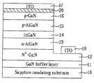
- FIG. 1is a schematic diagram of an LED having an insulating substrate according to a better embodiment of the present invention.
- FIG. 1a schematic diagram of an LED having an insulating substrate according to a better embodiment of the present invention.
- the LEDincludes a stacked structure, which is composed of a sapphire insulating substrate 10 , a GaN buffer layer 11 positioned on the insulating substrate 10 , an n + -type GaN contact layer 12 positioned on the buffer layer 11 , an n-type AlGaN cladding layer 13 positioned on the n + -type contact layer 12 , an InGaN light-emitting layer 14 with a multiple-quantum well (MQW) structure positioned on the n-type cladding layer 13 , a p-type AlGaN cladding layer 15 positioned on the light-emitting layer 14 , a p-type GaN contact layer 16 positioned on the p-type cladding layer 15 , and an n + -type InGaN reverse-tunneling layer 20 positioned on the p-type contact layer 16 .
- n + -type contact layer 12Since sapphire is dielectric, a portion of the stacked structure of the LED has to be etched, exposing a portion of the n + -type contact layer 12 . Following this, an ITO layer is formed on the exposed surface of the LED. A photolithographic process is then used to form a p-type transparent ohmic contact electrode 17 on the n + -type reverse-tunneling layer 20 , and form an n-type transparent ohmic contact electrode 19 on the exposed portion of the n + -type contact layer 12 , respectively.
- the n + -type reverse-tunneling layer 20has a high carrier concentration of approximately 1.5 ⁇ 10 20 cm ⁇ 3 , a thickness of approximately 20 angstroms, and provides high transparency.
- the p-n junction between the reverse-tunneling layer 20 and the contact layer 16 , and the p-n junction between the cladding layers 15 and 13must be in opposite bias conditions to induce electron tunneling through the reverse-tunneling layer 20 according to a tunneling effect.
- the p-n junction between the reverse-tunneling layer 20 and the contact layer 16is in a forward bias condition
- the p-n junction between the cladding layers 15 and 13must be in a reverse bias condition.
- the p-n junction between the reverse-tunneling layer 20 and the contact layer 16is in a reverse bias condition
- the p-n junction between the cladding layers 15 and 13must be in a forward bias condition.
- the multiple-quantum well structure for the InGaN light-emitting layer 14can be replaced with a single-quantum well structure.
- the GaN buffer layer 11 and/or the p-type contact layer 16can be optional to be removed from the LED structure.
- the n+-type GaN contact layer 12can be replaced by an n-type GaN layer.
- the p-type transparent ohmic contact electrode 17 and the n-type transparent ohmic contact electrode 19 of the LED of the present inventionare made of the same materials, such as ITO, CTO or TiWN. Therefore, the manufacturing procedures of LEDs are simplified, and the production costs are effectively reduced according to the present invention.
Landscapes
- Led Devices (AREA)
- Electrodes Of Semiconductors (AREA)
Abstract
Description
1. Field of the Invention
The present invention relates to a light emitting diode (LED), and more particularly, to a light emitting diode having an insulating substrate.
2. Description of the Prior Art
Light emitting diodes (LEDs) are employed in a wide variety of applications including optical display devices, traffic lights, data storage equipment, communication devices, illumination apparatuses, and medical treatment equipment. One of the main goals of engineers who design LEDs is to increase the brightness of the light emitted from LEDs.
U.S. Pat. No. 5,563,422 discloses a gallium nitride (GaN)-based LED in FIG. 10. The LED has a p-type ohmic contact electrode 56 made of nickel, gold or a nickel-gold alloy. The LED also has an n-type ohmic contact electrode 57 made of titanium, aluminum, or a titanium-aluminum alloy. Since the electrodes 56 and 57 are made of different materials, two evaporation processes and two photolithographic processes are required to form the electrodes 56 and 57, respectively.
It is an objective of the claimed invention to provide an LED having a p-type ohmic contact electrode and an n-type ohmic contact electrode made of the same materials.
According to the claimed invention, the LED includes an insulating substrate; a buffer layer positioned on the insulating substrate; an n+-type contact layer positioned on the buffer layer, the contact layer having a first surface and a second surface; an n-type cladding layer positioned on the first surface of the n+-type contact layer; a light-emitting layer positioned on the n-type cladding layer; a p-type cladding layer positioned on the light-emitting layer; a p-type contact layer positioned on the p-type cladding layer; an n+-type reverse-tunneling layer positioned on the p-type contact layer; a p-type transparent ohmic contact electrode positioned on the n+-type reverse-tunneling layer; and an n-type transparent ohmic contact electrode positioned on the second surface of the n+-type contact layer. The p-type transparent ohmic contact electrode and the n-type transparent ohmic contact electrode are made of the same materials.
It is an advantage of the claimed invention that the p-type ohmic contact electrode and the n-type ohmic contact electrode are made of the same materials, thus only an evaporation process and a photolithographic process are required for simultaneously forming the p-type ohmic contact electrode and the n-type ohmic contact electrode to reduce the production costs of the LED.
These and other objectives of the claimed invention will no doubt become obvious to those of ordinary skill in the art after reading the following detailed description of the preferred embodiment that is illustrated in the various figures and drawings.
Please refer toFIG. 1 of a schematic diagram of an LED having an insulating substrate according to a better embodiment of the present invention. The LED includes a stacked structure, which is composed of asapphire insulating substrate 10, aGaN buffer layer 11 positioned on theinsulating substrate 10, an n+-typeGaN contact layer 12 positioned on thebuffer layer 11, an n-typeAlGaN cladding layer 13 positioned on the n+-type contact layer 12, an InGaN light-emittinglayer 14 with a multiple-quantum well (MQW) structure positioned on the n-type cladding layer 13, a p-typeAlGaN cladding layer 15 positioned on the light-emittinglayer 14, a p-typeGaN contact layer 16 positioned on the p-type cladding layer 15, and an n+-type InGaN reverse-tunneling layer 20 positioned on the p-type contact layer 16.
Since sapphire is dielectric, a portion of the stacked structure of the LED has to be etched, exposing a portion of the n+-type contact layer 12. Following this, an ITO layer is formed on the exposed surface of the LED. A photolithographic process is then used to form a p-type transparentohmic contact electrode 17 on the n+-type reverse-tunneling layer 20, and form an n-type transparentohmic contact electrode 19 on the exposed portion of the n+-type contact layer 12, respectively.
In a better embodiment of the present invention, the n+-type reverse-tunneling layer 20 has a high carrier concentration of approximately 1.5×1020cm−3, a thickness of approximately20 angstroms, and provides high transparency. The p-n junction between the reverse-tunneling layer 20 and thecontact layer 16, and the p-n junction between thecladding layers tunneling layer 20 according to a tunneling effect. For example, when p-n junction between the reverse-tunneling layer 20 and thecontact layer 16 is in a forward bias condition, the p-n junction between thecladding layers tunneling layer 20 and thecontact layer 16 is in a reverse bias condition, the p-n junction between thecladding layers
In addition, in other embodiments of the present invention, the multiple-quantum well structure for the InGaN light-emitting layer 14 can be replaced with a single-quantum well structure. TheGaN buffer layer 11 and/or the p-type contact layer 16 can be optional to be removed from the LED structure. The n+-typeGaN contact layer 12 can be replaced by an n-type GaN layer.
In contrast to the prior art, the p-type transparentohmic contact electrode 17 and the n-type transparentohmic contact electrode 19 of the LED of the present invention are made of the same materials, such as ITO, CTO or TiWN. Therefore, the manufacturing procedures of LEDs are simplified, and the production costs are effectively reduced according to the present invention.
Those skilled in the art will readily observe that numerous modifications and alterations of the device may be made while retaining the teachings of the invention. Accordingly, the above disclosure should be construed as limited only by the metes and bounds of the appended claims.
Claims (14)
1. A light emitting diode comprising:
an insulating substrate;
a semiconductor stack positioned over the insulating substrate, the semiconductor stack comprising a first surface and a second surface, a distance between the first surface and the insulating substrate is greater than a distance between the second surface and the insulating substrate;
a reverse-tunneling layer over the first surface, the reverse-tunneling layer being a gallium nitride (GaN) based semiconductor;
a first transparent ohmic contact electrode positioned directly on the reverse-tunneling layer, the first transparent ohmic contact electrode comprising an oxide; and
a second transparent ohmic contact electrode positioned over the second surface.
2. The light emitting diode ofclaim 1 , wherein the insulating substrate comprises sapphire, and the first transparent ohmic contact electrode and the second transparent ohmic contact electrode comprise the same non-metal material.
3. The light emitting diode ofclaim 1 , wherein the first transparent ohmic contact electrode or the second transparent ohmic contact electrode comprises at least one selected from a group comprising indium tin oxide (ITO) and cadmium tin oxide (CTO).
4. A light emitting diode comprising:
an insulating substrate;
a buffer layer positioned on the insulating substrate;
an n+-type contact layer positioned on the buffer layer, the contact layer comprising a first surface and a second surface;
an n-type cladding layer positioned on the first surface of the n+-type contact layer;
a light-emitting layer positioned on the n-type cladding layer;
a p-type cladding layer positioned on the light-emitting layer;
a p-type contact layer positioned on the p-type cladding layer;
an n+-type reverse-tunneling layer positioned on the p-type contact layer;
a p-type transparent ohmic contact electrode positioned on the n+-type reverse-tunneling layer; and
an n-type transparent ohmic contact electrode positioned on the second surface of the n+-type contact layer;
wherein the p-type transparent ohmic contact electrode and the n-type transparent ohmic contact electrode comprise the same materials.
5. The light emitting diode ofclaim 4 , wherein the insulating substrate comprises sapphire.
6. The light emitting diode ofclaim 4 , wherein the p-type transparent ohmic contact electrode and the n-type transparent ohmic contact electrode are made of at least one selected from a group comprising indium tin oxide and cadmium tin oxide.
7. A light emitting diode comprising:
an insulating substrate;
a semiconductor light emitting stack positioned over the insulating substrate, the semiconductor light emitting stack comprising a first surface and a second surface, a distance between the first surface and the insulating substrate is greater than a distance between the second surface and the insulating substrate;
a reverse-tunneling layer over the first surface, the reverse-tunneling layer being a gallium nitride (GaN) based semiconductor;
a first non-metal transparent ohmic contact electrode positioned over the reverse-tunneling layer; and
a second non-metal transparent ohmic contact electrode positioned over the second surface,
wherein the first non-metal transparent ohmic contact electrode and the second non-metal transparent ohmic contact electrode comprise the same oxide material.
8. The light emitting diode ofclaim 7 , wherein the first non-metal transparent ohmic contact electrode and the second non-metal transparent ohmic contact electrode comprise at least one selected from a group comprising indium tin oxide (ITO) and cadmium tin oxide (CTO).
9. A light emitting diode comprising:
an insulating substrate;
a semiconductor stack positioned over the insulating substrate, the semiconductor stack comprising a first surface and a second surface, a distance between the first surface and the insulating substrate is greater than a distance between the second surface and the insulating substrate;
a reverse-tunneling layer, which is a gallium nitride (GaN) based semiconductor that has a carrier concentration of approximately 1.5×1020cm−3, over the first surface;
a first transparent ohmic contact electrode directly on the reverse-tunneling layer, the first transparent ohmic contact electrode comprising an oxide; and
a second transparent ohmic contact electrode over the second surface.
10. The light emitting diode ofclaim 9 , wherein the reverse-tunneling layer has a thickness of approximately 20 angstroms.
11. A light emitting diode comprising:
an insulating substrate;
a semiconductor stack positioned over the insulating substrate, the semiconductor stack comprising a first surface and a second surface, a distance between the first surface and the insulating substrate is greater than a distance between the second surface and the insulating substrate;
a reverse-tunneling layer over the first surface, the reverse-tunneling layer being a gallium nitride (GaN) based semiconductor; and
a first transparent ohmic contact electrode directly on the reverse-tunneling layer, the first transparent ohmic contact electrode comprising an oxide.
12. A light emitting diode comprising:
an insulating substrate;
a buffer layer positioned on the insulating substrate;
an n-type contact layer positioned on the buffer layer, the contact layer comprising a first surface and a second surface;
an n-type cladding layer positioned on the first surface of the n-type contact layer;
a light-emitting layer positioned on the n-type cladding layer;
a p-type cladding layer positioned on the light-emitting layer;
a p-type contact layer positioned on the p-type cladding layer;
an n+-type reverse-tunneling layer positioned on the p-type contact layer;
a p-type transparent ohmic contact electrode positioned on the n+-type reverse-tunneling layer; and
an n-type transparent ohmic contact electrode positioned on the second surface of the n+-type contact layer;
wherein the p-type transparent ohmic contact electrode and the n-type transparent ohmic contact electrode comprise the same materials.
13. The light emitting diode ofclaim 12 , wherein the insulating substrate comprises sapphire.
14. The light emitting diode ofclaim 12 , wherein the p-type transparent ohmic contact electrode and the n-type transparent ohmic contact electrode are made of at least one selected from a group comprising indium tin oxide and cadmium tin oxide.
Applications Claiming Priority (2)
| Application Number | Priority Date | Filing Date | Title |
|---|---|---|---|
| TW090113284ATW493287B (en) | 2001-05-30 | 2001-05-30 | Light emitting diode structure with non-conductive substrate |
| TW090113284 | 2001-05-30 |
Publications (2)
| Publication Number | Publication Date |
|---|---|
| US20020179918A1 US20020179918A1 (en) | 2002-12-05 |
| US6936860B2true US6936860B2 (en) | 2005-08-30 |
Family
ID=21678407
Family Applications (1)
| Application Number | Title | Priority Date | Filing Date |
|---|---|---|---|
| US10/063,822Expired - LifetimeUS6936860B2 (en) | 2001-05-30 | 2002-05-16 | Light emitting diode having an insulating substrate |
Country Status (3)
| Country | Link |
|---|---|
| US (1) | US6936860B2 (en) |
| JP (1) | JP3786898B2 (en) |
| TW (1) | TW493287B (en) |
Cited By (17)
| Publication number | Priority date | Publication date | Assignee | Title |
|---|---|---|---|---|
| US20050191179A1 (en)* | 2004-02-27 | 2005-09-01 | Mu-Jen Lai | Structure and manufacturing of gallium nitride light emitting diode |
| US20060243988A1 (en)* | 2005-05-02 | 2006-11-02 | Nichia Corporation | Nitride semiconductor element |
| US20070252135A1 (en)* | 2004-08-26 | 2007-11-01 | Lee Suk H | Nitride Semiconductor Light Emitting Device and Fabrication Method Thereof |
| US20090095975A1 (en)* | 2006-03-09 | 2009-04-16 | Sumsung Electo-Mechanics Co., Ltd. | Light emitting diode package |
| US20100015742A1 (en)* | 2008-07-18 | 2010-01-21 | Au Optronics Corporation | Method for fabricating light emitting diode chip |
| US20100065816A1 (en)* | 2003-07-18 | 2010-03-18 | Seong Jae Kim | Light emitting diode and fabrication method thereof |
| US20100155754A1 (en)* | 2006-02-16 | 2010-06-24 | Sumitomo Chemical Company, Limited | Group III Nitride Semiconductor Light Emitting Device and Method for Producing the Same |
| US7772604B2 (en) | 2006-01-05 | 2010-08-10 | Illumitex | Separate optical device for directing light from an LED |
| US7789531B2 (en) | 2006-10-02 | 2010-09-07 | Illumitex, Inc. | LED system and method |
| US7829358B2 (en) | 2008-02-08 | 2010-11-09 | Illumitex, Inc. | System and method for emitter layer shaping |
| US20110042645A1 (en)* | 2005-07-06 | 2011-02-24 | Lg Innotek Co., Ltd. | Nitride semiconductor led and fabrication method thereof |
| US8115217B2 (en) | 2008-12-11 | 2012-02-14 | Illumitex, Inc. | Systems and methods for packaging light-emitting diode devices |
| US20130017639A1 (en)* | 2011-07-12 | 2013-01-17 | Toyoda Gosei Co., Ltd. | Method for producing a group iii nitride semiconductor light-emitting device |
| US8449128B2 (en) | 2009-08-20 | 2013-05-28 | Illumitex, Inc. | System and method for a lens and phosphor layer |
| US20130175553A1 (en)* | 2012-01-06 | 2013-07-11 | Phostek, Inc. | Light-emitting diode device |
| US8585253B2 (en) | 2009-08-20 | 2013-11-19 | Illumitex, Inc. | System and method for color mixing lens array |
| US12087877B2 (en) | 2021-02-05 | 2024-09-10 | Toyoda Gosei Co., Ltd. | Light-emitting element |
Families Citing this family (53)
| Publication number | Priority date | Publication date | Assignee | Title |
|---|---|---|---|---|
| TW546859B (en)* | 2002-09-20 | 2003-08-11 | Formosa Epitaxy Inc | Structure and manufacturing method of GaN light emitting diode |
| US20050082575A1 (en)* | 2002-10-29 | 2005-04-21 | Lung-Chien Chen | Structure and manufacturing method for GaN light emitting diodes |
| TW577184B (en)* | 2002-12-26 | 2004-02-21 | Epistar Corp | Light emitting layer having voltage/resistance interdependent layer |
| US7358539B2 (en)* | 2003-04-09 | 2008-04-15 | Lumination Llc | Flip-chip light emitting diode with indium-tin-oxide based reflecting contacts |
| KR100525545B1 (en) | 2003-06-25 | 2005-10-31 | 엘지이노텍 주식회사 | Nitride semiconductor LED and fabrication method for thereof |
| US7560750B2 (en)* | 2003-06-26 | 2009-07-14 | Kyocera Corporation | Solar cell device |
| JP2007504639A (en)* | 2003-08-29 | 2007-03-01 | オスラム オプト セミコンダクターズ ゲゼルシャフト ミット ベシュレンクテル ハフツング | Radiation emission semiconductor device |
| CN100345314C (en)* | 2004-01-18 | 2007-10-24 | 泰谷光电科技股份有限公司 | Method for manufacturing gallium nitride transparent conductive oxide film ohmic electrode |
| KR100486614B1 (en)* | 2004-03-05 | 2005-05-03 | 에피밸리 주식회사 | Ⅲ-Nitride compound semiconductor light emitting device with low contact resistance |
| KR20050093319A (en)* | 2004-03-18 | 2005-09-23 | 삼성전기주식회사 | Nitride-based semiconductor led having improved luminous efficiency and fabrication method thereof |
| US7385226B2 (en)* | 2004-03-24 | 2008-06-10 | Epistar Corporation | Light-emitting device |
| TWI237402B (en) | 2004-03-24 | 2005-08-01 | Epistar Corp | High luminant device |
| JP2006295104A (en) | 2004-07-23 | 2006-10-26 | Semiconductor Energy Lab Co Ltd | LIGHT EMITTING ELEMENT AND LIGHT EMITTING DEVICE USING THE SAME |
| CN100524850C (en)* | 2004-09-23 | 2009-08-05 | 璨圆光电股份有限公司 | Gallium Nitride Light Emitting Diode Structure |
| JP2006156590A (en)* | 2004-11-26 | 2006-06-15 | Mitsubishi Cable Ind Ltd | Light emitting diode |
| KR100661709B1 (en)* | 2004-12-23 | 2006-12-26 | 엘지이노텍 주식회사 | Nitride semiconductor light emitting device and manufacturing method |
| US8097897B2 (en) | 2005-06-21 | 2012-01-17 | Epistar Corporation | High-efficiency light-emitting device and manufacturing method thereof |
| US9508902B2 (en) | 2005-02-21 | 2016-11-29 | Epistar Corporation | Optoelectronic semiconductor device |
| JP4967243B2 (en)* | 2005-03-08 | 2012-07-04 | 三菱化学株式会社 | GaN-based light emitting diode and light emitting device |
| US7804100B2 (en)* | 2005-03-14 | 2010-09-28 | Philips Lumileds Lighting Company, Llc | Polarization-reversed III-nitride light emitting device |
| JP2006261358A (en)* | 2005-03-17 | 2006-09-28 | Fujitsu Ltd | Semiconductor light emitting device |
| JP4956902B2 (en)* | 2005-03-18 | 2012-06-20 | 三菱化学株式会社 | GaN-based light emitting diode and light emitting device using the same |
| KR100609117B1 (en)* | 2005-05-03 | 2006-08-08 | 삼성전기주식회사 | Nitride-based semiconductor light emitting device and its manufacturing method |
| JP2006313773A (en)* | 2005-05-06 | 2006-11-16 | Sumitomo Electric Ind Ltd | Semiconductor device and manufacturing method thereof |
| KR100878433B1 (en)* | 2005-05-18 | 2009-01-13 | 삼성전기주식회사 | Method for manufacturing ohmic contact layer of light emitting device and method for manufacturing light emitting device using same |
| US8405106B2 (en) | 2006-10-17 | 2013-03-26 | Epistar Corporation | Light-emitting device |
| TW200717843A (en)* | 2005-10-19 | 2007-05-01 | Epistar Corp | Light-emitting element with high-light-extracting-efficiency |
| US9530940B2 (en) | 2005-10-19 | 2016-12-27 | Epistar Corporation | Light-emitting device with high light extraction |
| US8928022B2 (en) | 2006-10-17 | 2015-01-06 | Epistar Corporation | Light-emitting device |
| WO2007136097A1 (en)* | 2006-05-23 | 2007-11-29 | Meijo University | Semiconductor light emitting element |
| JP2008034822A (en) | 2006-06-28 | 2008-02-14 | Nichia Chem Ind Ltd | Semiconductor light emitting device |
| CN100514775C (en)* | 2006-09-20 | 2009-07-15 | 中国科学院半导体研究所 | A method for making GaN base laser tube core |
| DE102006057747B4 (en) | 2006-09-27 | 2015-10-15 | Osram Opto Semiconductors Gmbh | Semiconductor body and semiconductor chip with a semiconductor body |
| DE102007018307A1 (en)* | 2007-01-26 | 2008-07-31 | Osram Opto Semiconductors Gmbh | Semiconductor chip and method for producing a semiconductor chip |
| CN102779918B (en) | 2007-02-01 | 2015-09-02 | 日亚化学工业株式会社 | Semiconductor light-emitting elements |
| JP2008244161A (en)* | 2007-03-27 | 2008-10-09 | Toyoda Gosei Co Ltd | Method for forming electrode of group III nitride compound semiconductor light emitting device |
| KR20080089859A (en)* | 2007-04-02 | 2008-10-08 | 엘지이노텍 주식회사 | Nitride semiconductor light emitting device and manufacturing method thereof |
| DE102007035687A1 (en)* | 2007-07-30 | 2009-02-05 | Osram Opto Semiconductors Gmbh | Optoelectronic component with a stack of layers |
| JP5126884B2 (en)* | 2008-01-16 | 2013-01-23 | シャープ株式会社 | Nitride semiconductor light emitting device and method for manufacturing nitride semiconductor light emitting device |
| JP2010003804A (en)* | 2008-06-19 | 2010-01-07 | Sharp Corp | Nitride semiconductor light-emitting diode element and method of manufacturing the same |
| TWI399868B (en)* | 2009-01-17 | 2013-06-21 | Semi Photonics Co Ltd | Methods for manufacturing light emitting diode having high reflective contact |
| JP5633560B2 (en) | 2010-03-23 | 2014-12-03 | 日亜化学工業株式会社 | Nitride semiconductor light emitting device |
| US20110291147A1 (en) | 2010-05-25 | 2011-12-01 | Yongjun Jeff Hu | Ohmic contacts for semiconductor structures |
| KR101201597B1 (en)* | 2011-03-25 | 2012-11-14 | 주식회사 퀀텀디바이스 | Light emitting device and manufacturing method thereof |
| US20120267658A1 (en)* | 2011-04-20 | 2012-10-25 | Invenlux Limited | Large-area light-emitting device and method for fabricating the same |
| JP5321656B2 (en)* | 2011-08-05 | 2013-10-23 | 三菱化学株式会社 | GaN-based light emitting diode and light emitting device |
| JP5304855B2 (en)* | 2011-08-12 | 2013-10-02 | 三菱化学株式会社 | GaN-based light emitting diode and light emitting device using the same |
| KR20130079873A (en)* | 2012-01-03 | 2013-07-11 | 엘지이노텍 주식회사 | Light emitting device and lighting system including the same |
| JP2013179176A (en)* | 2012-02-28 | 2013-09-09 | Mitsubishi Chemicals Corp | Nitride semiconductor chip manufacturing method |
| JP5811413B2 (en)* | 2013-03-21 | 2015-11-11 | ウシオ電機株式会社 | LED element |
| TWI730096B (en)* | 2016-05-20 | 2021-06-11 | 荷蘭商露明控股公司 | Light emitting devices and methods for growing the same |
| JP6727185B2 (en) | 2017-12-28 | 2020-07-22 | 日機装株式会社 | Nitride semiconductor light emitting device |
| TWI750664B (en) | 2020-05-19 | 2021-12-21 | 錼創顯示科技股份有限公司 | Micro light emitting diode chip |
Citations (9)
| Publication number | Priority date | Publication date | Assignee | Title |
|---|---|---|---|---|
| JPH08102550A (en) | 1994-09-30 | 1996-04-16 | Rohm Co Ltd | Semiconductor light emitting element |
| JPH0974246A (en) | 1995-09-07 | 1997-03-18 | Mitsubishi Electric Corp | Semiconductor laser |
| US5889295A (en)* | 1996-02-26 | 1999-03-30 | Kabushiki Kaisha Toshiba | Semiconductor device |
| US5900650A (en)* | 1995-08-31 | 1999-05-04 | Kabushiki Kaisha Toshiba | Semiconductor device and method of manufacturing the same |
| US6020602A (en)* | 1996-09-10 | 2000-02-01 | Kabushiki Kaisha Toshba | GaN based optoelectronic device and method for manufacturing the same |
| US6078064A (en)* | 1998-05-04 | 2000-06-20 | Epistar Co. | Indium gallium nitride light emitting diode |
| US6121635A (en)* | 1997-04-15 | 2000-09-19 | Kabushiki Kaisha Toshiba | Semiconductor light-emitting element having transparent electrode and current blocking layer, and semiconductor light-emitting including the same |
| US6121634A (en)* | 1997-02-21 | 2000-09-19 | Kabushiki Kaisha Toshiba | Nitride semiconductor light emitting device and its manufacturing method |
| US6288416B1 (en)* | 1995-03-17 | 2001-09-11 | Toyoda Gosei Co., Ltd. | Light-emitting semiconductor device using group III nitride compound |
- 2001
- 2001-05-30TWTW090113284Apatent/TW493287B/ennot_activeIP Right Cessation
- 2002
- 2002-05-16USUS10/063,822patent/US6936860B2/ennot_activeExpired - Lifetime
- 2002-05-29JPJP2002156095Apatent/JP3786898B2/ennot_activeExpired - Lifetime
Patent Citations (9)
| Publication number | Priority date | Publication date | Assignee | Title |
|---|---|---|---|---|
| JPH08102550A (en) | 1994-09-30 | 1996-04-16 | Rohm Co Ltd | Semiconductor light emitting element |
| US6288416B1 (en)* | 1995-03-17 | 2001-09-11 | Toyoda Gosei Co., Ltd. | Light-emitting semiconductor device using group III nitride compound |
| US5900650A (en)* | 1995-08-31 | 1999-05-04 | Kabushiki Kaisha Toshiba | Semiconductor device and method of manufacturing the same |
| JPH0974246A (en) | 1995-09-07 | 1997-03-18 | Mitsubishi Electric Corp | Semiconductor laser |
| US5889295A (en)* | 1996-02-26 | 1999-03-30 | Kabushiki Kaisha Toshiba | Semiconductor device |
| US6020602A (en)* | 1996-09-10 | 2000-02-01 | Kabushiki Kaisha Toshba | GaN based optoelectronic device and method for manufacturing the same |
| US6121634A (en)* | 1997-02-21 | 2000-09-19 | Kabushiki Kaisha Toshiba | Nitride semiconductor light emitting device and its manufacturing method |
| US6121635A (en)* | 1997-04-15 | 2000-09-19 | Kabushiki Kaisha Toshiba | Semiconductor light-emitting element having transparent electrode and current blocking layer, and semiconductor light-emitting including the same |
| US6078064A (en)* | 1998-05-04 | 2000-06-20 | Epistar Co. | Indium gallium nitride light emitting diode |
Cited By (50)
| Publication number | Priority date | Publication date | Assignee | Title |
|---|---|---|---|---|
| US8674337B2 (en) | 2003-07-18 | 2014-03-18 | Lg Innotek Co., Ltd. | Gallium nitride based light emitting diode and fabrication method thereof |
| US7884388B2 (en)* | 2003-07-18 | 2011-02-08 | Lg Innotek Co., Ltd | Light emitting diode having a first GaN layer and a first semiconductor layer each having a predetermined thickness and fabrication method therof |
| US20100136732A1 (en)* | 2003-07-18 | 2010-06-03 | Seong Jae Kim | Light emitting diode and fabrication method thereof |
| US7989235B2 (en)* | 2003-07-18 | 2011-08-02 | Lg Innotek Co., Ltd | Light emitting diode and fabrication method thereof |
| US9362454B2 (en) | 2003-07-18 | 2016-06-07 | Lg Innotek Co., Ltd. | Gallium nitride based light emitting diode |
| US8927960B2 (en) | 2003-07-18 | 2015-01-06 | Lg Innotek Co., Ltd. | Gallium nitride based light emitting diode |
| US8680571B2 (en) | 2003-07-18 | 2014-03-25 | Lg Innotek Co., Ltd. | Gallium nitride based light emitting diode |
| US20100065816A1 (en)* | 2003-07-18 | 2010-03-18 | Seong Jae Kim | Light emitting diode and fabrication method thereof |
| US7208752B2 (en)* | 2004-02-27 | 2007-04-24 | Supernova Optoelectronics Corporation | Structure and manufacturing of gallium nitride light emitting diode |
| US20050191179A1 (en)* | 2004-02-27 | 2005-09-01 | Mu-Jen Lai | Structure and manufacturing of gallium nitride light emitting diode |
| US20070252135A1 (en)* | 2004-08-26 | 2007-11-01 | Lee Suk H | Nitride Semiconductor Light Emitting Device and Fabrication Method Thereof |
| US8053794B2 (en) | 2004-08-26 | 2011-11-08 | Lg Innotek Co., Ltd | Nitride semiconductor light emitting device and fabrication method thereof |
| US20060243988A1 (en)* | 2005-05-02 | 2006-11-02 | Nichia Corporation | Nitride semiconductor element |
| US8076694B2 (en) | 2005-05-02 | 2011-12-13 | Nichia Corporation | Nitride semiconductor element having a silicon substrate and a current passing region |
| US20110042645A1 (en)* | 2005-07-06 | 2011-02-24 | Lg Innotek Co., Ltd. | Nitride semiconductor led and fabrication method thereof |
| US8089082B2 (en) | 2005-07-06 | 2012-01-03 | Lg Innotek Co., Ltd. | Nitride semiconductor LED and fabrication method thereof |
| US9574743B2 (en) | 2006-01-05 | 2017-02-21 | Illumitex, Inc. | Separate optical device for directing light from an LED |
| US8896003B2 (en) | 2006-01-05 | 2014-11-25 | Illumitex, Inc. | Separate optical device for directing light from an LED |
| US7772604B2 (en) | 2006-01-05 | 2010-08-10 | Illumitex | Separate optical device for directing light from an LED |
| US7968896B2 (en) | 2006-01-05 | 2011-06-28 | Illumitex, Inc. | Separate optical device for directing light from an LED |
| US8097891B2 (en) | 2006-02-16 | 2012-01-17 | Sumitomo Chemical Company, Limited | Group III nitride semiconductor light emitting device and method for producing the same |
| US20100155754A1 (en)* | 2006-02-16 | 2010-06-24 | Sumitomo Chemical Company, Limited | Group III Nitride Semiconductor Light Emitting Device and Method for Producing the Same |
| US20090095975A1 (en)* | 2006-03-09 | 2009-04-16 | Sumsung Electo-Mechanics Co., Ltd. | Light emitting diode package |
| US7789531B2 (en) | 2006-10-02 | 2010-09-07 | Illumitex, Inc. | LED system and method |
| US8087960B2 (en) | 2006-10-02 | 2012-01-03 | Illumitex, Inc. | LED system and method |
| US8263993B2 (en) | 2008-02-08 | 2012-09-11 | Illumitex, Inc. | System and method for emitter layer shaping |
| US7829358B2 (en) | 2008-02-08 | 2010-11-09 | Illumitex, Inc. | System and method for emitter layer shaping |
| US8173466B2 (en) | 2008-07-18 | 2012-05-08 | Lextar Electronics Corp. | Method for fabricating LED chip comprising reduced mask count and lift-off processing |
| US20100015742A1 (en)* | 2008-07-18 | 2010-01-21 | Au Optronics Corporation | Method for fabricating light emitting diode chip |
| US8173465B2 (en) | 2008-07-18 | 2012-05-08 | Lextar Electronics Corp. | Method for fabricating LED chip comprising reduced mask count and lift-off processing |
| US8173467B2 (en) | 2008-07-18 | 2012-05-08 | Lextar Electronics Corp. | Method for fabricating LED chip comprising reduced mask count and lift-off processing |
| US7927901B2 (en) | 2008-07-18 | 2011-04-19 | Lextar Electronics Corp. | Method for fabricating LED chip comprising reduced mask count and lift-off processing |
| US8173468B2 (en) | 2008-07-18 | 2012-05-08 | Lextar Electronics Corp. | Method for fabricating LED chip comprising reduced mask count and lift-off processing |
| US8178377B2 (en) | 2008-07-18 | 2012-05-15 | Lextar Electronics Corp. | Method for fabricating lED chip comprising reduced mask count |
| US8178376B2 (en) | 2008-07-18 | 2012-05-15 | Lextar Electronics Corp. | Method for fabricating LED chip comprising reduced mask count and lift-off processing |
| US20110165706A1 (en)* | 2008-07-18 | 2011-07-07 | Lextar Electronics Corp. | Method for Fabricating LED Chip Comprising Reduced Mask Count and Lift-Off Processing |
| US20110159613A1 (en)* | 2008-07-18 | 2011-06-30 | Lextar Electronics Corp. | Method for Fabricating LED Chip Comprising Reduced Mask Count and Lift-Off Processing |
| US20110159623A1 (en)* | 2008-07-18 | 2011-06-30 | Lextar Electronics Corp. | Method for Fabricating LED Chip Comprising Reduced Mask Count and Lift-Off Processing |
| US20110159614A1 (en)* | 2008-07-18 | 2011-06-30 | Lextar Electronics Corp. | Method for Fabricating LED Chip Comprising Reduced Mask Count and Lift-Off Processing |
| US20110159612A1 (en)* | 2008-07-18 | 2011-06-30 | Lextar Electronics Corp. | Method for Fabricating LED Chip Comprising Reduced Mask Count and Lift-Off Processing |
| US20110165705A1 (en)* | 2008-07-18 | 2011-07-07 | Lextar Electronics Corp. | Method for Fabricating LED Chip Comprising Reduced Mask Count and Lift-Off Processing |
| US8115217B2 (en) | 2008-12-11 | 2012-02-14 | Illumitex, Inc. | Systems and methods for packaging light-emitting diode devices |
| US8585253B2 (en) | 2009-08-20 | 2013-11-19 | Illumitex, Inc. | System and method for color mixing lens array |
| US9086211B2 (en) | 2009-08-20 | 2015-07-21 | Illumitex, Inc. | System and method for color mixing lens array |
| US8449128B2 (en) | 2009-08-20 | 2013-05-28 | Illumitex, Inc. | System and method for a lens and phosphor layer |
| US8980657B2 (en)* | 2011-07-12 | 2015-03-17 | Toyoda Gosei Co., Ltd. | Method for producing a group III nitride semiconductor light-emitting device |
| US20130017639A1 (en)* | 2011-07-12 | 2013-01-17 | Toyoda Gosei Co., Ltd. | Method for producing a group iii nitride semiconductor light-emitting device |
| US20130175553A1 (en)* | 2012-01-06 | 2013-07-11 | Phostek, Inc. | Light-emitting diode device |
| US9130103B2 (en)* | 2012-01-06 | 2015-09-08 | Phostek, Inc. | Light-emitting diode device |
| US12087877B2 (en) | 2021-02-05 | 2024-09-10 | Toyoda Gosei Co., Ltd. | Light-emitting element |
Also Published As
| Publication number | Publication date |
|---|---|
| US20020179918A1 (en) | 2002-12-05 |
| JP3786898B2 (en) | 2006-06-14 |
| TW493287B (en) | 2002-07-01 |
| JP2003060236A (en) | 2003-02-28 |
Similar Documents
| Publication | Publication Date | Title |
|---|---|---|
| US6936860B2 (en) | Light emitting diode having an insulating substrate | |
| US7385226B2 (en) | Light-emitting device | |
| US9299884B2 (en) | Light emitting device and light emitting device package including the same | |
| KR101953716B1 (en) | Light emitting device, light emitting device package, and lighting system | |
| US8344353B2 (en) | Light emitting diode having a transparent substrate | |
| JP5911198B2 (en) | Light emitting element | |
| CN104201267B (en) | Luminescent device, light emitting device package and illuminator | |
| KR20050036737A (en) | Nitride light emitting device | |
| US20120175592A1 (en) | Light-emitting device | |
| KR101990095B1 (en) | Light emitting device, method for fabricating the same, and light emitting device package | |
| JP2014135490A (en) | Light-emitting element | |
| KR101916020B1 (en) | Light emitting device, method for fabricating the same, and light emitting device package | |
| KR101843420B1 (en) | Light emitting device, method for fabricating the same, and light emitting device package | |
| JP2006013500A (en) | Light emitting device | |
| KR20130009040A (en) | Light emitting device, method of fabricating light emitting device, light emitting device package, and light unit | |
| KR102199998B1 (en) | Light emitting device | |
| US20240290912A1 (en) | Light emitting diode and light emitting device | |
| KR20130038061A (en) | Light emitting device, method of fabricating light emitting device, light emitting device package, and light unit | |
| KR100710087B1 (en) | Formation method of light emitting diode | |
| KR102404760B1 (en) | Light emitting device | |
| CN118431364A (en) | Light emitting diodes and light emitting devices | |
| KR101856215B1 (en) | Light emitting device and light emitting device package | |
| KR101826980B1 (en) | Light emitting device, method for fabricating the same, and light emitting device package | |
| CN118173683A (en) | Light emitting diode and light emitting device | |
| KR20140090823A (en) | Light emitting device, light emitting device package, and light unit |
Legal Events
| Date | Code | Title | Description |
|---|---|---|---|
| AS | Assignment | Owner name:EPISTAR CORPORATION, TAIWAN Free format text:ASSIGNMENT OF ASSIGNORS INTEREST;ASSIGNORS:SUNG, SHU-WEN;KU, CHIN-FU;LIU, CHIA-CHENG;AND OTHERS;REEL/FRAME:012696/0780 Effective date:20020430 | |
| AS | Assignment | Owner name:EPISTAR CORPORATION, TAIWAN Free format text:ASSIGNMENT OF ASSIGNORS INTEREST;ASSIGNORS:OU, CHEN;CHANG, CHUAN-MING;REEL/FRAME:015936/0975 Effective date:20050418 | |
| STCF | Information on status: patent grant | Free format text:PATENTED CASE | |
| FPAY | Fee payment | Year of fee payment:4 | |
| AS | Assignment | Owner name:FORMOSA EPITAXY INCORPORATION,TAIWAN Free format text:DECLARATION;ASSIGNOR:EPISTAR CORPORATION;REEL/FRAME:024523/0799 Effective date:20100604 | |
| FPAY | Fee payment | Year of fee payment:8 | |
| FPAY | Fee payment | Year of fee payment:12 |