US6936849B1 - Silicon carbide gate transistor - Google Patents
Silicon carbide gate transistorDownload PDFInfo
- Publication number
- US6936849B1 US6936849B1US08/903,486US90348697AUS6936849B1US 6936849 B1US6936849 B1US 6936849B1US 90348697 AUS90348697 AUS 90348697AUS 6936849 B1US6936849 B1US 6936849B1
- Authority
- US
- United States
- Prior art keywords
- silicon carbide
- gate
- memory device
- region
- channel
- Prior art date
- Legal status (The legal status is an assumption and is not a legal conclusion. Google has not performed a legal analysis and makes no representation as to the accuracy of the status listed.)
- Expired - Fee Related
Links
Images


Classifications
- H—ELECTRICITY
- H01—ELECTRIC ELEMENTS
- H01L—SEMICONDUCTOR DEVICES NOT COVERED BY CLASS H10
- H01L21/00—Processes or apparatus adapted for the manufacture or treatment of semiconductor or solid state devices or of parts thereof
- H01L21/02—Manufacture or treatment of semiconductor devices or of parts thereof
- H01L21/04—Manufacture or treatment of semiconductor devices or of parts thereof the devices having potential barriers, e.g. a PN junction, depletion layer or carrier concentration layer
- H01L21/18—Manufacture or treatment of semiconductor devices or of parts thereof the devices having potential barriers, e.g. a PN junction, depletion layer or carrier concentration layer the devices having semiconductor bodies comprising elements of Group IV of the Periodic Table or AIIIBV compounds with or without impurities, e.g. doping materials
- H01L21/28—Manufacture of electrodes on semiconductor bodies using processes or apparatus not provided for in groups H01L21/20 - H01L21/268
- H01L21/28008—Making conductor-insulator-semiconductor electrodes
- H01L21/28255—Making conductor-insulator-semiconductor electrodes the insulator being formed after the semiconductor body, the semiconductor belonging to Group IV and not being elemental silicon, e.g. Ge, SiGe, SiGeC
- H—ELECTRICITY
- H10—SEMICONDUCTOR DEVICES; ELECTRIC SOLID-STATE DEVICES NOT OTHERWISE PROVIDED FOR
- H10D—INORGANIC ELECTRIC SEMICONDUCTOR DEVICES
- H10D30/00—Field-effect transistors [FET]
- H10D30/60—Insulated-gate field-effect transistors [IGFET]
- H—ELECTRICITY
- H10—SEMICONDUCTOR DEVICES; ELECTRIC SOLID-STATE DEVICES NOT OTHERWISE PROVIDED FOR
- H10D—INORGANIC ELECTRIC SEMICONDUCTOR DEVICES
- H10D84/00—Integrated devices formed in or on semiconductor substrates that comprise only semiconducting layers, e.g. on Si wafers or on GaAs-on-Si wafers
- H10D84/01—Manufacture or treatment
- H10D84/0123—Integrating together multiple components covered by H10D12/00 or H10D30/00, e.g. integrating multiple IGBTs
- H10D84/0126—Integrating together multiple components covered by H10D12/00 or H10D30/00, e.g. integrating multiple IGBTs the components including insulated gates, e.g. IGFETs
- H10D84/0165—Integrating together multiple components covered by H10D12/00 or H10D30/00, e.g. integrating multiple IGBTs the components including insulated gates, e.g. IGFETs the components including complementary IGFETs, e.g. CMOS devices
- H10D84/0172—Manufacturing their gate conductors
- H—ELECTRICITY
- H10—SEMICONDUCTOR DEVICES; ELECTRIC SOLID-STATE DEVICES NOT OTHERWISE PROVIDED FOR
- H10D—INORGANIC ELECTRIC SEMICONDUCTOR DEVICES
- H10D84/00—Integrated devices formed in or on semiconductor substrates that comprise only semiconducting layers, e.g. on Si wafers or on GaAs-on-Si wafers
- H10D84/01—Manufacture or treatment
- H10D84/02—Manufacture or treatment characterised by using material-based technologies
- H10D84/03—Manufacture or treatment characterised by using material-based technologies using Group IV technology, e.g. silicon technology or silicon-carbide [SiC] technology
- H10D84/038—Manufacture or treatment characterised by using material-based technologies using Group IV technology, e.g. silicon technology or silicon-carbide [SiC] technology using silicon technology, e.g. SiGe
- Y—GENERAL TAGGING OF NEW TECHNOLOGICAL DEVELOPMENTS; GENERAL TAGGING OF CROSS-SECTIONAL TECHNOLOGIES SPANNING OVER SEVERAL SECTIONS OF THE IPC; TECHNICAL SUBJECTS COVERED BY FORMER USPC CROSS-REFERENCE ART COLLECTIONS [XRACs] AND DIGESTS
- Y10—TECHNICAL SUBJECTS COVERED BY FORMER USPC
- Y10S—TECHNICAL SUBJECTS COVERED BY FORMER USPC CROSS-REFERENCE ART COLLECTIONS [XRACs] AND DIGESTS
- Y10S438/00—Semiconductor device manufacturing: process
- Y10S438/931—Silicon carbide semiconductor
Definitions
- the present inventionrelates generally to integrated circuits, and particularly to a silicon carbide gate field-effect transistor and complementary metal-oxide-semiconductor (CMOS) compatible method of fabrication.
- CMOScomplementary metal-oxide-semiconductor
- FETsField-effect transistors
- CMOScomplementary metal-oxide-semiconductor
- a standard CMOS processis typically used to fabricate FETs that each have a gate electrode that is composed of n-type conductively doped polycrystalline silicon (polysilicon) material.
- the intrinsic properties of the polysilicon gate materialaffect operating characteristics of the FET that is fabricated using a standard CMOS process.
- Siliconmonocrystalline and polycrystalline
- E genergy band gap
- ⁇electron affinity
- ⁇electron affinity
- V Tturn-on threshold voltage
- the V T magnitudemust be downwardly adjusted by doping the channel region that underlies the gate electrode of the FET.
- Doping to adjust the V T magnitudetypically includes the ion-implantation of acceptor dopants, such as boron, through the polysilicon gate material and an underlying gate insulator into the channel region of the underlying silicon substrate.
- acceptor dopantssuch as boron
- V T magnitude adjustment by ion-implantationis particularly difficult to carry out in semiconductor-on-insulator (SOI) and other thin film transistor technology.
- SOIsemiconductor-on-insulator
- the FET channel regionis formed in a semiconductor layer that is formed upon an insulating region of the substrate.
- the semiconductor layermay be only 1000 ⁇ thick, making it difficult to obtain a sufficiently sharply defined dopant distribution through ion-implantation.
- polysilicon gate FETsAnother drawback of polysilicon gate FETs is that their intrinsic characteristics are likely to change during subsequent high temperature process steps.
- the polysilicon gateis typically doped with boron impurities that have a high diffusivity in polysilicon. Because of this high diffusion rate, the boron impurities that are introduced into the polysilicon gate electrode of the FET diffuse through the underlying gate oxide during subsequent high temperature processing steps. As a result, the V T magnitude the FETs may change during these subsequent high temperature processing steps.
- Halvis et al.U.S. Pat. No. 5,369,040 discloses a charge-coupled device (CCD) photodetector which has transparent gate MOS imaging transistors fabricated from polysilicon with the addition of up to 50% carbon, and preferably about 10% carbon, which makes the gate material more transparent to the visible portion of the energy spectrum.
- CCDcharge-coupled device
- the Halvis et al. patentis directed to improving gate transmissivity to allow a greater portion of incident light in the visible spectrum to penetrate the gate.
- Halvis et al.did not recognize the need to improve the gate characteristics of FETs by lowering V T magnitudes or stabilizing V T magnitudes over subsequent thermal processing steps.
- Halvis et al.does not disclose or suggest the use of carbon in a field-effect transistor gate in the absence of incident light.
- the above described needsare unresolved in the art of fabrication of FETs using CMOS processes.
- One aspect of the present inventionprovides a field-effect transistor (FET) having an electrically interconnected gate formed of polycrystalline or microcrystalline silicon carbide (SiC) material.
- the SiC gate materialhas a lower electron affinity and a higher work function than a polysilicon gate material.
- the characteristics of the SiC gate FETinclude a lower threshold voltage (V T ) magnitude and a lower tunneling barrier voltage as compared to polysilicon gate FETs.
- Another aspect of the inventionprovides a method for fabricating a transistor including an electrically interconnected SiC gate.
- Source and drain regionsare fabricated in a silicon substrate, separated from each other and defining a channel region therebetween.
- An insulating regionis fabricated over the channel region.
- a SiC gateis fabricated over the insulating region.
- SiC gate fabricationincludes depositing an SiC layer on the insulating region using low pressure chemical vapor deposition (LPCVD) and etching the SiC material to a desired pattern using a reactive ion etch (RIE) process.
- LPCVDlow pressure chemical vapor deposition
- RIEreactive ion etch
- the SiC gate FETprovides lower V T magnitudes, allowing integrated circuit operation at lower power supply voltages.
- the lower power supply voltageprovides advantages including lower power consumption and ease in downward scaling of transistor dimensions without unacceptably increasing electric fields.
- the lower V T magnitudesalso enable higher switching speeds and improved performance.
- the SiC gate FETalso provides lower V T magnitudes without adjustment by ion-implantation. This is particularly useful for semiconductor-on-insulator (SOI) and other thin film transistor devices in which an adequately sharply defined dopant distribution is difficult to obtain by ion-implantation V T adjustment.
- SOIsemiconductor-on-insulator
- the SiC gate FETalso provides V T magnitudes that are stable in spite of subsequent thermal processing steps.
- the SiC gate FETfurther provides more optimal V T magnitudes for n-channel FETs (e.g., enhancement rather than depletion mode).
- FIG. 1is a cross-sectional view, illustrating generally one embodiment of a transistor according to one aspect of the invention, including a silicon carbide (SiC) gate.
- SiCsilicon carbide
- FIG. 1Ais a cross-sectional view, illustrating generally one embodiment of a transistor according to one aspect of the invention, including a silicon carbide (SiC) gate and a semiconductor surface layer formed on an underlying insulating portion.
- SiCsilicon carbide
- FIG. 2is a graph, illustrating generally barrier height versus tunneling distance for a SiC gate transistor.
- FIGS. 3A-3Hillustrate generally examples of process steps for fabricating n-channel and p-channel SiC gate transistors.
- FIG. 4is a simplified block diagram, illustrating generally one embodiment of a semiconductor memory device incorporating SiC gate transistors.
- wafer and substrate used in the following descriptioninclude any semiconductor-based structure having an exposed surface with which to form the integrated circuit structure of the invention. Wafer and substrate are used interchangeably to refer to semiconductor structures during processing, and may include other layers that have been fabricated thereupon.
- Both wafer and substrateinclude doped and undoped semiconductors, epitaxial semiconductor layers supported by a base semiconductor or insulator, as well as other semiconductor structures well known to one skilled in the art.
- doped and undoped semiconductorsepitaxial semiconductor layers supported by a base semiconductor or insulator, as well as other semiconductor structures well known to one skilled in the art.
- the following detailed descriptionis, therefore, not to be taken in a limiting sense, and the scope of the present invention is defined only by the appended claims.
- the present inventiondiscloses a field-effect transistor (FET) having a gate that is formed of a polycrystalline or microcrystalline silicon carbide (SiC) material, which includes any material that incorporates both silicon and carbon into the gate region of a FET.
- the SiC gate FETincludes characteristics such as, for example, a lower electron affinity and a higher work function than a conventional polycrystalline silicon (polysilicon) gate FET.
- the FET gateis electrically interconnected or otherwise driven by an input signal.
- the SiC gate FETprovides lower threshold voltage (V T ) magnitudes, allowing operation at lower power supply voltages. This, in turn, allows lower power consumption, and facilitates the downward scaling of transistor dimensions without increasing electric fields unacceptably.
- the lower V T magnitudesalso enable higher switching speeds and improved performance.
- the SiC gate FETalso provides lower V T magnitudes without adjustment by ion-implantation. This is particularly useful for semiconductor-on-insulator (SOI) and other thin film transistor devices in which a sufficiently sharp doping profile is difficult to obtain by ion-implantation.
- the SiC gate FETalso includes V T magnitudes that are stable in spite of subsequent thermal processing steps.
- the SiC gate FETfurther provides more optimal threshold voltage magnitudes for n-channel FETs (e.g., enhancement rather than depletion mode).
- the SiC gate FETfurther provides floating gate transistors having lower tunneling barriers, such as described in Forbes U.S. Pat. No. 5,801,401 issued Sep.
- Flash Memory with Microcrystalline Silicon Carbide Film Floating Gatewhich is assigned to the assignee of the present application and which is herein incorporated by reference. This allows faster storage and removal of charge from the floating gates, and is particularly useful for speeding erasing and writing operations in flash electrically erasable and programmable read-only memories (EEPROMs) and other applications.
- EEPROMselectrically erasable and programmable read-only memories
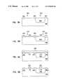
- FIG. 1is a cross-sectional view illustrating generally, by way of example, one embodiment of a n-channel FET provided by the invention.
- the FETincludes a source region 102 , a drain region 104 and a gate region 106 .
- source 102 and drain 104are fabricated by forming highly doped (n+) regions in a lightly doped (p ⁇ ) silicon semiconductor substrate 108 .
- substrate 108includes a thin semiconductor surface layer formed on an underlying insulating portion, such as in a SOI or other thin film transistor process technology.
- Source 102 and drain 104are separated by a predetermined length in which a channel region 110 is formed.
- gate 106is formed of SiC material.
- the silicon carbide material forming gate 106is described more generally as Si 1 ⁇ x C x .
- the SiC gate materialis approximately stoichiometric, i.e., x ⁇ 0.5.
- other embodiments of the inventioncould include less carbon, i.e., x ⁇ 0.5, or more carbon, i.e., x>0.5.
- one embodiment of the SiC gate materialis illustrated by 0.1 ⁇ x ⁇ 0.5.
- Another example embodimentis illustrated by way of example, but not by way of limitation, by 0.4 ⁇ x ⁇ 0.6.
- the SiC gate materialcan include either or both polycrystalline or microcrystalline embodiments of the SiC gate material.
- an insulating layersuch as silicon dioxide (oxide) 114 or other insulating layer, is formed by chemical vapor deposition (CVD).
- Oxide 114isolates gate 106 from other layers, such as layer 112 .
- gate 106is oxidized to form at least a portion of oxide 114 to isolate gate 106 from other layers such as layer 112 .
- layer 112is a polysilicon control gate in a floating gate transistor in an electrically erasable and programmable read-only memory (EEPROM) memory cell.
- EEPROMelectrically erasable and programmable read-only memory
- gate 106is floating (electrically isolated) for charge storage thereupon, such as by known EEPROM techniques.
- layer 112is a metal or other conductive interconnection line that is located above gate 106 .
- Gate 106is isolated from channel 110 by an insulating layer such as thin oxide layer 118 , or any other suitable dielectric material.
- thin oxide layer 118is a gate oxide layer that can be approximately 100 angstroms ( ⁇ ) thick, such as for conventional FET operation.
- thin oxide layer 118is a tunnel oxide material that can be approximately 50-100 ⁇ thick.
- the SiC gate 106has particular advantages over polysilicon gates used in FETs fabricated using a conventional complementary metal-oxide-semiconductor (CMOS) process due to different characteristics of the SiC material.
- CMOScomplementary metal-oxide-semiconductor
- SiCis a wide bandgap semiconductor material with a bandgap energy of about 2.1 eV, in contrast to silicon (monocrystalline or polycrystalline), which has a bandgap energy of about 1.2 eV.
- SiChas an electron affinity of about 3.7 to 3.8 eV, in contrast to silicon, which has an electron affinity of about 4.2 eV.
- the smaller electron affinity of the SiC gate 106 materialreduces the barrier potential at the interface between gate 106 and thin oxide layer 118 .
- thin oxide layer 118is a tunnel oxide in a floating gate transistor EEPROM memory cell
- the lower electron affinity of SiCreduces the tunneling distance and increases the tunneling probability. This speeds the write and erase operations of storing and removing charge by Fowler-Nordheim tunneling to and from the gate 106 , which is a floating gate. This is particularly advantageous for “flash” EEPROMs in which many floating gate transistor memory cells must be erased simultaneously. The large charge that must be transported by Fowler-Nordheim tunneling during the erasure of a flash EEPROM typically results in relatively long erasure times. By reducing the tunneling distance and increasing the tunneling probability, the SiC gate 106 reduces erasure times in flash EEPROMs.
- P-type SiCalso has a larger work function than polysilicon, providing other advantages for a FET having a SiC gate 106 , particularly in an electrically interconnected or driven gate embodiment of the present invention.
- large work function gatesprovide advantages for FETs fabricated using SOI starting material and process technology.
- p-channel polysilicon gate FETstypically operate as fully depleted thin film transistor devices and require V T magnitude adjustment by ion-implantation.
- V T magnitude adjustment by ion-implantationis difficult because the semiconductor layer may be only 1000 ⁇ thick, making it difficult to obtain a sufficiently sharply defined dopant distribution through ion-implantation.
- the p-type SiC gatehas a larger work function than polysilicon, thereby providing reduced V T magnitudes for p-channel FETs without adjustment by ion-implantation.
- the reduced V T magnitudes of the p-channel FETsadvantageously allows operation at lower power supply voltages. This, in turn, lowers power consumption and facilitates the downward scaling of FET dimensions without increasing electric fields unacceptably.
- the reduced V T magnitudesalso enable higher switching speeds and improved integrated circuit performance.
- the V T magnitudes obtained according to the present inventionare stable in spite of subsequent thermal processing steps, since no migratory dopants are ion-implanted to adjust the p-channel V T magnitude. Such lower V T magnitudes and accompanying advantages are difficult to achieve by other integrated circuit manufacturing techniques.
- p-type SiC gatesalso provide advantages for n-channel FETs. For example, while polysilicon gate FETs tend to result in depletion mode n-channel V T magnitudes, ptype SiC gates more easily provide enhancement mode operation, which is often a more desirable device characteristic for designing integrated circuits.
- FIG. 1Ais a cross-sectional view illustrating generally, by way of example, another embodiment of an n-channel FET 128 provided by the invention.
- a source region 102 and a drain region 104are formed in a thin semiconductor surface layer 130 that is formed on an underlying insulating portion 132 .
- the other elements of the FET 128are similar to the corresponding elements in the n-channel FET shown in FIG. 1 , and have retained the same reference numerals for purposes of brevity.
- FIG. 2illustrates generally how the smaller electron affinity provides a smaller barrier potential.
- the smaller barrier potentialreduces the distance that electrons stored on the gate have to traverse by Fowler-Nordheim tunneling to be stored upon or removed from the polycrystalline or microcrystalline SiC gate 106 .
- the reduced tunneling distanceallows easier charge transfer, such as during writing or erasing data in a floating gate transistor in a flash EEPROM memory cell.
- “do”represents the tunneling distance of a typical polysilicon floating gate transistor due to the barrier height represented by the dashed line “OLD”.
- the tunneling distance “dn”corresponds to a SiC gate and its smaller barrier height represented by the dashed line “SNEW”.
- the increased tunneling probability of the SiC gate 106advantageously provides faster programming and erasure times for SiC gate floating gate transistors in flash EEPROM memories. Flash EEPROM memories using lower V T magnitude SiC gate floating gate transistors also operate at lower power supply voltages, as described above.
- the transistor of FIG. 1illustrates generally, by way of example, an n-channel FET that includes an SiC gate.
- the transistorcan be formed on substrate 108 using an n-well CMOS process, enabling monolithic CMOS fabrication of n-channel and p-channel FETs on a common substrate.
- both the n-channel and the p-channel FETsinclude a polycrystalline or microcrystalline SiC gate.
- the FET illustrated in FIG. 1could also represent a p-channel FET.
- Applications of the p-channel and n-channel SiC gate FETsinclude any application in which conventionally formed polysilicon gate FETs are used.
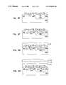
- FIGS. 3A-3Hillustrate generally examples of process steps for fabricating n-channel and p-channel SiC gate transistors according to the present invention.
- the n-channel and p-channel FETscan be produced on a silicon or other semiconductor substrate, an SOI substrate, or any other suitable substrate 108 . Only the process steps that differ from conventional CMOS process technology are described in detail.
- substrate 108undergoes conventional CMOS processing up to the formation of the gate structure, including formation of field oxide 300 for defining active regions 302 , and the formation of well regions, such as n-well 304 in which p-channel transistors will be fabricated.
- an insulating layersuch as thin oxide layer 118 is formed on substrate 108 , such as by dry thermal oxidation, including over the portions of the active area regions 302 in which n-channel and p-channel FETs are formed.
- thin oxide layer 118is a gate oxide layer that can be approximately 100 angstroms ( ⁇ ) thick.
- thin oxide layer 118is a tunnel oxide material that can be approximately 50-100 ⁇ thick.
- a thin film 306 of conductively doped polycrystalline or microcrystalline SiCis then deposited, such as by chemical vapor deposition (CVD) over the entire wafer, including over thin oxide layer 118 .
- the chemical composition of thin film 306may be different for the particular deposition conditions of the polycrystalline and microcrystalline SiC, as illustrated by way of the particular examples described above.
- n+ doped (e.g., phosphorus as dopant) gate regionsfor both p-channel and n-channel FETs, even thought p+ doped (e.g., boron as dopant) gate regions would provide more desirable operating characteristics. This is because boron easily diffuses out of the polysilicon gate regions during subsequent high temperature processing steps.
- one aspect of the present inventionis that it allows formation of n+ doped or p+ doped SiC gate regions. Since the diffusion rate of the boron dopant is lower in SiC than in polysilicon, boron can be used as a dopant in the SiC gate material.
- one advantage of the present inventionis that the V T magnitudes in the SiC gate FETs are less affected by subsequent high temperature process steps than those of conventional polysilicon gate FETs. This allows greater control of the V T magnitudes in the SiC gate FETs of the present invention.
- SiC film 306is deposited using low-pressure chemical vapor deposition (LPCVD), providing the structure illustrated in FIG. 3 C.
- LPCVDlow-pressure chemical vapor deposition
- the LPCVD processuses either a hot-wall reactor or a cold-wall reactor with a reactive gas, such as a mixture of Si(CH 3 ) 4 and Ar. Examples of such processes are disclosed in an article by Y. Yamaguchi et al., entitled “Properties of Heteroepitaxial 3C-SiC Films Grown by LPCVD”, in the 8 th-International Conference on Solid-State Sensors and Actuators and Eurosensors IX. Digest of Technical Papers, page 3. vol. (934+1030+85), pages 190-3, Vol.
- SiC film 306can be deposited using other techniques such as, for example, enhanced CVD techniques known to those skilled in the art including low pressure rapid thermal chemical vapor deposition (LP-RTCVD), or by decomposition of hexamethyl disalene using ArF excimer laser irradiation, or by low temperature molecular beam epitaxy (MBE).
- LP-RTCVDlow pressure rapid thermal chemical vapor deposition
- MBElow temperature molecular beam epitaxy
- SiC film 306examples include reactive magnetron sputtering, DC plasma discharge, ion-beam assisted deposition, ion-beam synthesis of amorphous SiC films, laser crystallization of amorphous SiC, laser reactive ablation deposition, and epitaxial growth by vacuum anneal.
- the conductivity of the SiC film 306can be changed by ion implantation during subsequent process steps, such as during the self-aligned formation of source/drain regions for the n-channel and p-channel FETs.
- SiC film 306is patterned and etched, together with the underlying thin oxide layer 118 , to form SiC gate 106 .
- SiC film 306is patterned using standard techniques and is etched using plasma etching, reactive ion etching (RIE) or a combination of these or other suitable methods.
- RIEreactive ion etching
- SiC film 306can be etched by RIE in a distributed cyclotron resonance reactor using a SF 6 /O2 gas mixture using SiO 2 as a mask with a selectivity of 6.5.
- Such processis known in the art and is disclosed, for example, in an article by F. Lanois, entitled “Angle Etch Control for Silicon Power Devices”, which appeared in Applied Physics Letters ; Vol 69, No.
- SiC film 306can be etched by RIE using the mixture SF 6 and O2 and F 2 /Ar/O 2 .
- An example of such a processis disclosed in an article by N. J. Dartnell, et al., entitled “Reactive Ion Etching of Silicon Carbide” in Vacuum , Vol. 46, No. 4, pages 349-355, 1955.
- the etch rate of SiC film 306can be significantly increased by using magnetron enhanced RIE.
- FIG. 3Eillustrates one embodiment in which SiC gate 106 is oxidized after formation, providing a thin layer 310 represented by the dashed line in FIG. 3 E.
- SiC gate 106can be oxidized, for example, by plasma oxidation similar to reoxidation of polycrystalline silicon. During the oxidation process, the carbon is oxidized as carbon monoxide or carbon dioxide and vaporizes, leaving the thin layer 310 of silicon oxide over SiC gate 106 .
- thin layer 310is used as, or as a portion of, an intergate dielectric between floating and control gates in a floating gate transistor embodiment of the present invention.
- FIG. 3Fillustrates generally a self-aligned embodiment of the formation of n-channel FET source/drain regions 312 and p-channel FET source/drain regions 314 for the p-channel FET.
- the doping of SiC gate 106can be changed by ion implantation, such as during the formation of n-channel FET source/drain regions 312 or p-channel FET source/drain regions 314 for the p-channel FET.
- a p-type SiC film 306can be deposited, and its doping then changed to n+ by leaving SiC gate 106 unmasked during the formation of the n+ source/drain regions 312 for the n-channel FET.
- FIG. 3Gillustrates generally the formation of an insulating layer, such as oxide 114 or other suitable insulator, after formation of n-channel FET source/drain regions 312 and p-channel FET source/drain regions 314 for the p-channel FET.
- oxide 114is deposited over the upper surface of the integrated circuit structure using a standard CVD process.
- Oxide 114isolates SiC gate 106 from other gates such as, for example, an overlying control gate layer 112 where SiC gate 106 is a floating gate in a floating gate transistor EEPROM memory cell.
- Oxide 114also isolates SiC gate 106 from any other conductive layer 112 , such as polysilicon layers, gates, metal lines, etc., that are fabricated above and over SiC gate 106 during subsequent process steps. Insulating layer 116 is produced on the structure in a conventional manner.
- FIG. 4is a simplified block diagram illustrating generally one embodiment of a memory 400 system incorporating SiC gate FETs according to one aspect of the present invention.
- the SiC gate FETsare used in various applications within memory 400 including, for example, in logic and output driver circuits.
- the SiC gate FETscan also function as memory cell access FETs, such as in a dynamic random access memory (DRAM) embodiment of memory 400 , or as other memory elements therein.
- memory 400is a flash EEPROM
- the SiC gate FETsare floating gate transistors that are used for nonvolatile storage of data as charge on the SiC floating gates.
- the SiC gate FETscan also be used in other types of memory systems, including SDRAM, SLDRAM and RDRAM devices, or in programmable logic arrays (PLAs), or in any other application in which transistors are used.
- PDAsprogrammable logic arrays
- FIG. 4illustrates, by way of example but not by way of limitation, a flash EEPROM memory 400 comprising a memory array 402 of multiple memory cells.
- Row decoder 404 and column decoder 406decode addresses provided on address lines 408 to access addressed SiC gate floating gate transistors in the memory cells in memory array 402 .
- Command and control circuitry 410controls the operation of memory 400 in response to control signals received on control lines 416 from a processor 401 or other memory controller during read, write, and erase operations.
- the floating SiC gates of the floating gate transistors in memory array 402advantageously reduce the tunneling distance and increase the tunneling probabilities, thereby speeding write and erase operations of memory 400 .
- Thisis particularly advantageous for “flash” EEPROMs in which many floating gate transistor memory cells must be erased simultaneously, which normally results in relatively long erasure times.
- the present inventionprovides a FET having a polycrystalline or microcrystalline SiC gate.
- the SiC gate FET characteristicsinclude a lower electron affinity and higher work function than a conventional polysilicon gate FET.
- the SiC gate FETprovides lower V T magnitudes, allowing operation at lower power supply voltages. This, in turn, lowers power consumption and facilitates downward scaling of transistor dimensions without increasing electric fields unacceptably.
- the lower V T magnitudesalso enable higher switching speeds and improved performance.
- the SiC gate FETalso provides lower V T magnitudes without adjustment by ion-implantation. This aspect of the invention is particularly useful for SOI, thin film transistors, and any other devices in which ion-implantation may not yield a sufficiently sharp dopant distribution.
- the SiC gate FETprovides V T magnitudes that are stable in spite of subsequent thermal processing steps.
- the SiC gate FETalso provides more optimal threshold voltage magnitudes for n-channel FETs (e.g., enhancement rather than depletion mode).
- the SiC gate FEThas an electrically interconnected or driven gate.
- the SiC gate FETfurther provides floating gate transistors that allow faster storage and erasure such as, for example, used in flash EEPROMs.
Landscapes
- Engineering & Computer Science (AREA)
- Physics & Mathematics (AREA)
- Condensed Matter Physics & Semiconductors (AREA)
- General Physics & Mathematics (AREA)
- Manufacturing & Machinery (AREA)
- Computer Hardware Design (AREA)
- Microelectronics & Electronic Packaging (AREA)
- Power Engineering (AREA)
- Thin Film Transistor (AREA)
- Semiconductor Memories (AREA)
- Non-Volatile Memory (AREA)
Abstract
Description
Claims (44)
Priority Applications (3)
| Application Number | Priority Date | Filing Date | Title |
|---|---|---|---|
| US08/903,486US6936849B1 (en) | 1997-07-29 | 1997-07-29 | Silicon carbide gate transistor |
| US09/133,943US6297521B1 (en) | 1997-07-29 | 1998-08-14 | Graded anti-reflective coating for IC lithography |
| US09/259,870US6835638B1 (en) | 1997-07-29 | 1999-03-01 | Silicon carbide gate transistor and fabrication process |
Applications Claiming Priority (1)
| Application Number | Priority Date | Filing Date | Title |
|---|---|---|---|
| US08/903,486US6936849B1 (en) | 1997-07-29 | 1997-07-29 | Silicon carbide gate transistor |
Related Child Applications (1)
| Application Number | Title | Priority Date | Filing Date |
|---|---|---|---|
| US09/259,870DivisionUS6835638B1 (en) | 1997-07-29 | 1999-03-01 | Silicon carbide gate transistor and fabrication process |
Publications (1)
| Publication Number | Publication Date |
|---|---|
| US6936849B1true US6936849B1 (en) | 2005-08-30 |
Family
ID=33541748
Family Applications (2)
| Application Number | Title | Priority Date | Filing Date |
|---|---|---|---|
| US08/903,486Expired - Fee RelatedUS6936849B1 (en) | 1997-07-29 | 1997-07-29 | Silicon carbide gate transistor |
| US09/259,870Expired - Fee RelatedUS6835638B1 (en) | 1997-07-29 | 1999-03-01 | Silicon carbide gate transistor and fabrication process |
Family Applications After (1)
| Application Number | Title | Priority Date | Filing Date |
|---|---|---|---|
| US09/259,870Expired - Fee RelatedUS6835638B1 (en) | 1997-07-29 | 1999-03-01 | Silicon carbide gate transistor and fabrication process |
Country Status (1)
| Country | Link |
|---|---|
| US (2) | US6936849B1 (en) |
Cited By (13)
| Publication number | Priority date | Publication date | Assignee | Title |
|---|---|---|---|---|
| US20010011900A1 (en)* | 1998-08-21 | 2001-08-09 | Hembree David R. | Methods of processing wafers and methods of communicating signals with respect to a wafer |
| US20030001191A1 (en)* | 1997-07-29 | 2003-01-02 | Micron Technology, Inc. | Dynamic electrically alterable programmable read only memory device |
| US20030059960A1 (en)* | 1998-02-27 | 2003-03-27 | Salman Akram | Methods of semiconductor processing |
| US20050146934A1 (en)* | 1997-07-29 | 2005-07-07 | Micron Technology, Inc. | Transistor with variable electron affinity gate and methods of fabrication and use |
| US20050219912A1 (en)* | 2002-04-15 | 2005-10-06 | Philippe Gendrier | Electrically erasable and programmable, non-volatile semiconductor memory device having a single layer of gate material, and corresponding memory plane |
| US20060017095A1 (en)* | 1997-07-29 | 2006-01-26 | Micron Technology, Inc. | Carburized silicon gate insulators for integrated circuits |
| US20060024878A1 (en)* | 1997-07-29 | 2006-02-02 | Micron Technology, Inc. | Deaprom having amorphous silicon carbide gate insulator |
| US20070051301A1 (en)* | 2005-02-22 | 2007-03-08 | Taisuke Hirooka | Method of manufacturing sic single crystal wafer |
| US20090258464A1 (en)* | 2008-04-09 | 2009-10-15 | International Business Machines Corporation | Methods for manufacturing a high voltage junction field effect transistor using a hybrid orientation technology wafer |
| US20090256174A1 (en)* | 2008-04-09 | 2009-10-15 | International Business Machines Corporation | Device structures for a high voltage junction field effect transistor manufactured using a hybrid orientation technology wafer and design structures for a high voltage integrated circuit |
| CN101303239B (en)* | 2007-05-10 | 2010-05-26 | 北方工业大学 | A sensor and its adjustment method |
| US20110001181A1 (en)* | 2009-07-06 | 2011-01-06 | Byoungsun Ju | Nonvolatile Memory Devices |
| US20110132448A1 (en)* | 2010-02-08 | 2011-06-09 | Suniva, Inc. | Solar cells and methods of fabrication thereof |
Families Citing this family (9)
| Publication number | Priority date | Publication date | Assignee | Title |
|---|---|---|---|---|
| US7081414B2 (en)* | 2003-05-23 | 2006-07-25 | Applied Materials, Inc. | Deposition-selective etch-deposition process for dielectric film gapfill |
| US7064050B2 (en)* | 2003-11-28 | 2006-06-20 | International Business Machines Corporation | Metal carbide gate structure and method of fabrication |
| US7045419B2 (en)* | 2003-12-12 | 2006-05-16 | Macronix International Co., Ltd. | Elimination of the fast-erase phenomena in flash memory |
| JPWO2007086196A1 (en)* | 2006-01-30 | 2009-06-18 | 住友電気工業株式会社 | Method for manufacturing silicon carbide semiconductor device |
| DE102007008562A1 (en)* | 2007-02-21 | 2008-08-28 | Qimonda Ag | Field effect transistor arrangement |
| US9018108B2 (en) | 2013-01-25 | 2015-04-28 | Applied Materials, Inc. | Low shrinkage dielectric films |
| US20170069497A1 (en)* | 2014-05-07 | 2017-03-09 | Tokyo Electron Limited | Plasma etching method |
| US9727123B1 (en) | 2016-05-13 | 2017-08-08 | Cypress Semiconductor Corporation | Configurable and power-optimized integrated gate-driver for USB power-delivery and type-C SoCs |
| CN107731929B (en)* | 2017-09-28 | 2019-12-13 | 信利(惠州)智能显示有限公司 | Method for manufacturing thin film transistor |
Citations (116)
| Publication number | Priority date | Publication date | Assignee | Title |
|---|---|---|---|---|
| US3792465A (en) | 1971-12-30 | 1974-02-12 | Texas Instruments Inc | Charge transfer solid state display |
| US4113515A (en) | 1975-06-04 | 1978-09-12 | U.S. Philips Corporation | Semiconductor manufacturing method using buried nitride formed by a nitridation treatment in the presence of active nitrogen |
| US4118795A (en) | 1976-08-27 | 1978-10-03 | Texas Instruments Incorporated | Two-phase CCD regenerator - I/O circuits |
| JPS57126175U (en) | 1981-01-27 | 1982-08-06 | ||
| US4384349A (en) | 1979-10-01 | 1983-05-17 | Texas Instruments Incorporated | High density electrically erasable floating gate dual-injection programmable memory device |
| US4460670A (en) | 1981-11-26 | 1984-07-17 | Canon Kabushiki Kaisha | Photoconductive member with α-Si and C, N or O and dopant |
| US4462150A (en) | 1981-11-10 | 1984-07-31 | Tokyo Shibaura Denki Kabushiki Kaisha | Method of forming energy beam activated conductive regions between circuit elements |
| US4473836A (en) | 1982-05-03 | 1984-09-25 | Dalsa Inc. | Integrable large dynamic range photodetector element for linear and area integrated circuit imaging arrays |
| US4507673A (en) | 1979-10-13 | 1985-03-26 | Tokyo Shibaura Denki Kabushiki Kaisha | Semiconductor memory device |
| JPS6024678Y2 (en) | 1980-12-01 | 1985-07-24 | 株式会社ダイフク | Conveyance device using a trolley |
| JPS60242678A (en) | 1984-05-17 | 1985-12-02 | Seiko Epson Corp | semiconductor storage device |
| JPS60184681U (en) | 1984-05-16 | 1985-12-07 | 株式会社 キングジム | slip holder |
| US4598305A (en) | 1984-06-18 | 1986-07-01 | Xerox Corporation | Depletion mode thin film semiconductor photodetectors |
| US4657699A (en) | 1984-12-17 | 1987-04-14 | E. I. Du Pont De Nemours And Company | Resistor compositions |
| JPS62122275U (en) | 1986-01-24 | 1987-08-03 | ||
| US4736317A (en)* | 1985-07-17 | 1988-04-05 | Syracuse University | Microprogram-coupled multiple-microprocessor module with 32-bit byte width formed of 8-bit byte width microprocessors |
| US4738729A (en) | 1984-10-19 | 1988-04-19 | Toshihiko Yoshida | Amorphous silicon semiconductor solar cell |
| US4768072A (en) | 1984-01-20 | 1988-08-30 | Fuji Electric Corporate Research And Development Co., Ltd. | Multilayer semiconductor device having an amorphous carbon and silicon layer |
| US4769686A (en) | 1983-04-01 | 1988-09-06 | Hitachi, Ltd. | Semiconductor device |
| JPS63219172A (en) | 1987-03-06 | 1988-09-12 | Hosiden Electronics Co Ltd | Thin-film transistor |
| JPS63181473U (en) | 1987-05-12 | 1988-11-22 | ||
| JPS63289960A (en)* | 1987-05-22 | 1988-11-28 | Fujitsu Ltd | Field-effect semiconductor device |
| US4816883A (en) | 1986-07-10 | 1989-03-28 | Sgs Microelettronica S.P.A. | Nonvolatile, semiconductor memory device |
| JPH01115162A (en) | 1987-10-29 | 1989-05-08 | Matsushita Electric Ind Co Ltd | Thin film transistor and its manufacturing method |
| US4841349A (en) | 1984-11-16 | 1989-06-20 | Fujitsu Limited | Semiconductor photodetector device with light responsive PN junction gate |
| US4849797A (en) | 1987-01-23 | 1989-07-18 | Hosiden Electronics Co., Ltd. | Thin film transistor |
| US4893273A (en) | 1985-03-28 | 1990-01-09 | Kabushiki Kaisha Toshiba | Semiconductor memory device for storing image data |
| US4897710A (en) | 1986-08-18 | 1990-01-30 | Sharp Kabushiki Kaisha | Semiconductor device |
| US4980303A (en) | 1987-08-19 | 1990-12-25 | Fujitsu Limited | Manufacturing method of a Bi-MIS semiconductor device |
| US4994401A (en) | 1987-01-16 | 1991-02-19 | Hosiden Electronics Co., Ltd. | Method of making a thin film transistor |
| US5049950A (en) | 1987-07-14 | 1991-09-17 | Sharp Kabushiki Kaisha | MIS structure photosensor |
| JPH03222367A (en) | 1990-01-26 | 1991-10-01 | Fujitsu Ltd | Insulated gate type field effect transistor |
| US5111430A (en) | 1989-06-22 | 1992-05-05 | Nippon Telegraph And Telephone Corporation | Non-volatile memory with hot carriers transmitted to floating gate through control gate |
| US5145741A (en) | 1989-06-05 | 1992-09-08 | Quick Nathaniel R | Converting ceramic materials to electrical conductors and semiconductors |
| JPH0456769B2 (en) | 1985-09-27 | 1992-09-09 | Ube Industries | |
| US5189504A (en) | 1989-12-11 | 1993-02-23 | Nippon Telegraph And Telephone Corporation | Semiconductor device of MOS structure having p-type gate electrode |
| US5235195A (en) | 1990-08-08 | 1993-08-10 | Minnesota Mining And Manufacturing Company | Solid state electromagnetic radiation detector with planarization layer |
| US5260593A (en) | 1991-12-10 | 1993-11-09 | Micron Technology, Inc. | Semiconductor floating gate device having improved channel-floating gate interaction |
| US5293560A (en) | 1988-06-08 | 1994-03-08 | Eliyahou Harari | Multi-state flash EEPROM system using incremental programing and erasing methods |
| US5298796A (en) | 1992-07-08 | 1994-03-29 | The United States Of America As Represented By The Administrator Of The National Aeronautics And Space Administration | Nonvolatile programmable neural network synaptic array |
| US5317535A (en) | 1992-06-19 | 1994-05-31 | Intel Corporation | Gate/source disturb protection for sixteen-bit flash EEPROM memory arrays |
| US5336361A (en) | 1990-03-23 | 1994-08-09 | Matsushita Electric Industrial Co., Ltd. | Method of manufacturing an MIS-type semiconductor device |
| JPH06224431A (en) | 1993-01-26 | 1994-08-12 | Sharp Corp | Thin-film transistor and liquid crystal display panel |
| JPH06302828A (en) | 1993-04-14 | 1994-10-28 | Matsushita Electric Ind Co Ltd | Nonvolatile semiconductor memory device |
| US5360491A (en) | 1993-04-07 | 1994-11-01 | The United States Of America As Represented By The United States Department Of Energy | β-silicon carbide protective coating and method for fabricating same |
| US5367306A (en)* | 1993-06-04 | 1994-11-22 | Hollon Blake D | GPS integrated ELT system |
| US5366713A (en) | 1992-06-03 | 1994-11-22 | Showa Shell Sekiyu K.K. | Method of forming p-type silicon carbide |
| US5369040A (en)* | 1992-05-18 | 1994-11-29 | Westinghouse Electric Corporation | Method of making transparent polysilicon gate for imaging arrays |
| US5371383A (en) | 1993-05-14 | 1994-12-06 | Kobe Steel Usa Inc. | Highly oriented diamond film field-effect transistor |
| US5388069A (en) | 1992-03-19 | 1995-02-07 | Fujitsu Limited | Nonvolatile semiconductor memory device for preventing erroneous operation caused by over-erase phenomenon |
| US5393999A (en) | 1993-02-22 | 1995-02-28 | Texas Instruments Incorporated | SiC power MOSFET device structure |
| US5407845A (en) | 1992-10-15 | 1995-04-18 | Fujitsu Limited | Method of manufacturing thin film transistors in a liquid crystal display apparatus |
| US5409501A (en) | 1991-07-15 | 1995-04-25 | Henkel Kommanditgesellschaft Auf Aktien | Dilutable aluminum triformate tanning agents in the form of highly concentrated, storable aqueous solutions and their use |
| JPH07115191A (en)* | 1993-02-23 | 1995-05-02 | Kobe Steel Ltd | Diamond field effect transistor and its manufacture |
| US5415126A (en) | 1993-08-16 | 1995-05-16 | Dow Corning Corporation | Method of forming crystalline silicon carbide coatings at low temperatures |
| US5424993A (en) | 1993-11-15 | 1995-06-13 | Micron Technology, Inc. | Programming method for the selective healing of over-erased cells on a flash erasable programmable read-only memory device |
| US5425860A (en) | 1993-04-07 | 1995-06-20 | The Regents Of The University Of California | Pulsed energy synthesis and doping of silicon carbide |
| US5438544A (en) | 1993-03-19 | 1995-08-01 | Fujitsu Limited | Non-volatile semiconductor memory device with function of bringing memory cell transistors to overerased state, and method of writing data in the device |
| US5441901A (en) | 1993-10-05 | 1995-08-15 | Motorola, Inc. | Method for forming a carbon doped silicon semiconductor device having a narrowed bandgap characteristic |
| JPH07226507A (en) | 1994-02-10 | 1995-08-22 | Fujitsu Ltd | Semiconductor device and manufacturing method thereof |
| US5449941A (en) | 1991-10-29 | 1995-09-12 | Semiconductor Energy Laboratory Co., Ltd. | Semiconductor memory device |
| US5455432A (en)* | 1994-10-11 | 1995-10-03 | Kobe Steel Usa | Diamond semiconductor device with carbide interlayer |
| US5465249A (en) | 1991-11-26 | 1995-11-07 | Cree Research, Inc. | Nonvolatile random access memory device having transistor and capacitor made in silicon carbide substrate |
| EP0681333A1 (en) | 1994-04-29 | 1995-11-08 | International Business Machines Corporation | Low voltage memory |
| US5467306A (en) | 1993-10-04 | 1995-11-14 | Texas Instruments Incorporated | Method of using source bias to increase threshold voltages and/or to correct for over-erasure of flash eproms |
| US5477485A (en) | 1995-02-22 | 1995-12-19 | National Semiconductor Corporation | Method for programming a single EPROM or FLASH memory cell to store multiple levels of data that utilizes a floating substrate |
| US5493140A (en) | 1993-07-05 | 1996-02-20 | Sharp Kabushiki Kaisha | Nonvolatile memory cell and method of producing the same |
| US5530581A (en) | 1995-05-31 | 1996-06-25 | Eic Laboratories, Inc. | Protective overlayer material and electro-optical coating using same |
| US5557122A (en) | 1995-05-12 | 1996-09-17 | Alliance Semiconductors Corporation | Semiconductor electrode having improved grain structure and oxide growth properties |
| US5557114A (en) | 1995-01-12 | 1996-09-17 | International Business Machines Corporation | Optical fet |
| JPH08255878A (en) | 1995-03-16 | 1996-10-01 | Fujitsu Ltd | Floating gate transistor and manufacturing method thereof |
| US5562769A (en) | 1991-12-20 | 1996-10-08 | Kobe Steel Usa, Inc. | Methods of forming diamond semiconductor devices and layers on nondiamond substrates |
| US5604357A (en) | 1994-07-12 | 1997-02-18 | Matsushita Electric Industrial Co., Ltd. | Semiconductor nonvolatile memory with resonance tunneling |
| US5623442A (en) | 1993-07-13 | 1997-04-22 | Nkk Corporation | Memory cells and memory devices with a storage capacitor of parasitic capacitance and information storing method using the same |
| US5623160A (en) | 1995-09-14 | 1997-04-22 | Liberkowski; Janusz B. | Signal-routing or interconnect substrate, structure and apparatus |
| US5654208A (en) | 1995-04-10 | 1997-08-05 | Abb Research Ltd. | Method for producing a semiconductor device having a semiconductor layer of SiC comprising a masking step |
| US5661312A (en) | 1995-03-30 | 1997-08-26 | Motorola | Silicon carbide MOSFET |
| US5670790A (en) | 1995-09-21 | 1997-09-23 | Kabushikik Kaisha Toshiba | Electronic device |
| US5672889A (en) | 1995-03-15 | 1997-09-30 | General Electric Company | Vertical channel silicon carbide metal-oxide-semiconductor field effect transistor with self-aligned gate for microwave and power applications, and method of making |
| US5698869A (en) | 1994-09-13 | 1997-12-16 | Kabushiki Kaisha Toshiba | Insulated-gate transistor having narrow-bandgap-source |
| US5714766A (en) | 1995-09-29 | 1998-02-03 | International Business Machines Corporation | Nano-structure memory device |
| US5719410A (en) | 1993-12-28 | 1998-02-17 | Kabushiki Kaisha Toshiba | Semiconductor device wiring or electrode |
| US5734181A (en) | 1995-09-14 | 1998-03-31 | Kabushiki Kaisha Toshiba | Semiconductor device and manufacturing method therefor |
| US5740104A (en) | 1997-01-29 | 1998-04-14 | Micron Technology, Inc. | Multi-state flash memory cell and method for programming single electron differences |
| US5754477A (en) | 1997-01-29 | 1998-05-19 | Micron Technology, Inc. | Differential flash memory cell and method for programming |
| US5786250A (en) | 1997-03-14 | 1998-07-28 | Micron Technology, Inc. | Method of making a capacitor |
| US5798548A (en) | 1995-05-18 | 1998-08-25 | Sanyo Electric Co., Ltd. | Semiconductor device having multiple control gates |
| US5801401A (en) | 1997-01-29 | 1998-09-01 | Micron Technology, Inc. | Flash memory with microcrystalline silicon carbide film floating gate |
| US5808336A (en) | 1994-05-13 | 1998-09-15 | Canon Kabushiki Kaisha | Storage device |
| US5828101A (en) | 1995-03-30 | 1998-10-27 | Kabushiki Kaisha Toshiba | Three-terminal semiconductor device and related semiconductor devices |
| US5846859A (en) | 1995-03-14 | 1998-12-08 | Samsung Electronics Co., Ltd. | Method for manufacturing a semiconductor memory device having capacitive storage |
| US5858811A (en) | 1994-11-28 | 1999-01-12 | Nec Corporation | Method for fabricating charge coupled device (CCD) as semiconductor device of MOS structure |
| US5861346A (en) | 1995-07-27 | 1999-01-19 | Regents Of The University Of California | Process for forming silicon carbide films and microcomponents |
| US5877041A (en) | 1997-06-30 | 1999-03-02 | Harris Corporation | Self-aligned power field effect transistor in silicon carbide |
| US5886368A (en)* | 1997-07-29 | 1999-03-23 | Micron Technology, Inc. | Transistor with silicon oxycarbide gate and methods of fabrication and use |
| US5886376A (en) | 1996-07-01 | 1999-03-23 | International Business Machines Corporation | EEPROM having coplanar on-insulator FET and control gate |
| US5886379A (en) | 1996-05-16 | 1999-03-23 | Lg Semicon Co., Ltd. | Semiconductor memory device with increased coupling ratio |
| US5898197A (en) | 1996-06-06 | 1999-04-27 | Sanyo Electric Co., Ltd. | Non-volatile semiconductor memory devices |
| US5907775A (en) | 1997-04-11 | 1999-05-25 | Vanguard International Semiconductor Corporation | Non-volatile memory device with high gate coupling ratio and manufacturing process therefor |
| US5912837A (en) | 1996-10-28 | 1999-06-15 | Micron Technology, Inc. | Bitline disturb reduction |
| US5926740A (en) | 1997-10-27 | 1999-07-20 | Micron Technology, Inc. | Graded anti-reflective coating for IC lithography |
| US5976926A (en) | 1996-11-12 | 1999-11-02 | Micron Technology, Inc. | Static memory cell and method of manufacturing a static memory cell |
| US5990531A (en) | 1995-12-28 | 1999-11-23 | Philips Electronics N.A. Corporation | Methods of making high voltage GaN-AlN based semiconductor devices and semiconductor devices made |
| US6018166A (en) | 1996-12-31 | 2000-01-25 | Industrial Technology Research Institute | Polysilicon carbon source/drain heterojunction thin-film transistor |
| US6031263A (en) | 1997-07-29 | 2000-02-29 | Micron Technology, Inc. | DEAPROM and transistor with gallium nitride or gallium aluminum nitride gate |
| US6034001A (en) | 1991-10-16 | 2000-03-07 | Kulite Semiconductor Products, Inc. | Method for etching of silicon carbide semiconductor using selective etching of different conductivity types |
| US6075259A (en) | 1994-11-14 | 2000-06-13 | North Carolina State University | Power semiconductor devices that utilize buried insulating regions to achieve higher than parallel-plane breakdown voltages |
| US6084248A (en) | 1996-06-28 | 2000-07-04 | Seiko Epson Corporation | Thin film transistor, manufacturing method thereof, and circuit and liquid crystal display device using the thin film transistor |
| US6093937A (en) | 1996-02-23 | 2000-07-25 | Semiconductor Energy Laboratory Co. Ltd. | Semiconductor thin film, semiconductor device and manufacturing method thereof |
| US6099574A (en) | 1996-12-19 | 2000-08-08 | Kabushiki Kaisha Toshiba | Method and apparatus for obtaining structure of semiconductor devices and memory for storing program for obtaining the same |
| US6130147A (en) | 1994-04-07 | 2000-10-10 | Sdl, Inc. | Methods for forming group III-V arsenide-nitride semiconductor materials |
| US6144581A (en) | 1996-07-24 | 2000-11-07 | California Institute Of Technology | pMOS EEPROM non-volatile data storage |
| US6163066A (en) | 1997-02-07 | 2000-12-19 | Micron Technology, Inc. | Porous silicon dioxide insulator |
| US6166768A (en) | 1994-01-28 | 2000-12-26 | California Institute Of Technology | Active pixel sensor array with simple floating gate pixels |
| US6271566B1 (en) | 1997-03-25 | 2001-08-07 | Toshiba Corporation | Semiconductor device having a carbon containing insulation layer formed under the source/drain |
| US6365919B1 (en) | 1998-09-02 | 2002-04-02 | Infineon Technologies Ag | Silicon carbide junction field effect transistor |
Family Cites Families (9)
| Publication number | Priority date | Publication date | Assignee | Title |
|---|---|---|---|---|
| JPS57126175A (en) | 1981-01-29 | 1982-08-05 | Kanegafuchi Chem Ind Co Ltd | Amorphous silicon carbide/amorophous silicon hetero junction optoelectric element |
| JPS6024678A (en) | 1983-07-21 | 1985-02-07 | Fujitsu Ltd | Image reading device |
| JPS60184681A (en) | 1984-03-02 | 1985-09-20 | Sharp Corp | Method for forming amorphous silicon carbide film for coating |
| JPS62122275A (en) | 1985-11-22 | 1987-06-03 | Mitsubishi Electric Corp | MIS type semiconductor device |
| GB2194905B (en) | 1986-07-21 | 1990-09-12 | Honda Motor Co Ltd | Fitting fly wheels and ignition coils to engines |
| JPS63181473A (en) | 1987-01-23 | 1988-07-26 | Hosiden Electronics Co Ltd | Thin-film transistor |
| JPH02203564A (en) | 1989-01-31 | 1990-08-13 | Sharp Corp | Silicon carbide semiconductor device |
| JPH0456769A (en) | 1990-06-22 | 1992-02-24 | Nippon Steel Corp | Formation of amorphous silicon carbide film containing microcrystal |
| JP3222367B2 (en) | 1995-10-11 | 2001-10-29 | 株式会社山武 | Temperature measurement circuit |
- 1997
- 1997-07-29USUS08/903,486patent/US6936849B1/ennot_activeExpired - Fee Related
- 1999
- 1999-03-01USUS09/259,870patent/US6835638B1/ennot_activeExpired - Fee Related
Patent Citations (127)
| Publication number | Priority date | Publication date | Assignee | Title |
|---|---|---|---|---|
| US3792465A (en) | 1971-12-30 | 1974-02-12 | Texas Instruments Inc | Charge transfer solid state display |
| US4113515A (en) | 1975-06-04 | 1978-09-12 | U.S. Philips Corporation | Semiconductor manufacturing method using buried nitride formed by a nitridation treatment in the presence of active nitrogen |
| US4118795A (en) | 1976-08-27 | 1978-10-03 | Texas Instruments Incorporated | Two-phase CCD regenerator - I/O circuits |
| US4384349A (en) | 1979-10-01 | 1983-05-17 | Texas Instruments Incorporated | High density electrically erasable floating gate dual-injection programmable memory device |
| US4507673A (en) | 1979-10-13 | 1985-03-26 | Tokyo Shibaura Denki Kabushiki Kaisha | Semiconductor memory device |
| JPS6024678Y2 (en) | 1980-12-01 | 1985-07-24 | 株式会社ダイフク | Conveyance device using a trolley |
| JPS57126175U (en) | 1981-01-27 | 1982-08-06 | ||
| US4462150A (en) | 1981-11-10 | 1984-07-31 | Tokyo Shibaura Denki Kabushiki Kaisha | Method of forming energy beam activated conductive regions between circuit elements |
| US4460670A (en) | 1981-11-26 | 1984-07-17 | Canon Kabushiki Kaisha | Photoconductive member with α-Si and C, N or O and dopant |
| US4473836A (en) | 1982-05-03 | 1984-09-25 | Dalsa Inc. | Integrable large dynamic range photodetector element for linear and area integrated circuit imaging arrays |
| US4769686A (en) | 1983-04-01 | 1988-09-06 | Hitachi, Ltd. | Semiconductor device |
| US4768072A (en) | 1984-01-20 | 1988-08-30 | Fuji Electric Corporate Research And Development Co., Ltd. | Multilayer semiconductor device having an amorphous carbon and silicon layer |
| JPS60184681U (en) | 1984-05-16 | 1985-12-07 | 株式会社 キングジム | slip holder |
| JPS60242678A (en) | 1984-05-17 | 1985-12-02 | Seiko Epson Corp | semiconductor storage device |
| US4598305A (en) | 1984-06-18 | 1986-07-01 | Xerox Corporation | Depletion mode thin film semiconductor photodetectors |
| US4738729A (en) | 1984-10-19 | 1988-04-19 | Toshihiko Yoshida | Amorphous silicon semiconductor solar cell |
| US4841349A (en) | 1984-11-16 | 1989-06-20 | Fujitsu Limited | Semiconductor photodetector device with light responsive PN junction gate |
| US4657699A (en) | 1984-12-17 | 1987-04-14 | E. I. Du Pont De Nemours And Company | Resistor compositions |
| US4893273A (en) | 1985-03-28 | 1990-01-09 | Kabushiki Kaisha Toshiba | Semiconductor memory device for storing image data |
| US4736317A (en)* | 1985-07-17 | 1988-04-05 | Syracuse University | Microprogram-coupled multiple-microprocessor module with 32-bit byte width formed of 8-bit byte width microprocessors |
| JPH0456769B2 (en) | 1985-09-27 | 1992-09-09 | Ube Industries | |
| JPS62122275U (en) | 1986-01-24 | 1987-08-03 | ||
| US4816883A (en) | 1986-07-10 | 1989-03-28 | Sgs Microelettronica S.P.A. | Nonvolatile, semiconductor memory device |
| US4897710A (en) | 1986-08-18 | 1990-01-30 | Sharp Kabushiki Kaisha | Semiconductor device |
| US4994401A (en) | 1987-01-16 | 1991-02-19 | Hosiden Electronics Co., Ltd. | Method of making a thin film transistor |
| US4849797A (en) | 1987-01-23 | 1989-07-18 | Hosiden Electronics Co., Ltd. | Thin film transistor |
| JPS63219172A (en) | 1987-03-06 | 1988-09-12 | Hosiden Electronics Co Ltd | Thin-film transistor |
| JPS63181473U (en) | 1987-05-12 | 1988-11-22 | ||
| JPS63289960A (en)* | 1987-05-22 | 1988-11-28 | Fujitsu Ltd | Field-effect semiconductor device |
| EP0291951B1 (en) | 1987-05-22 | 1993-08-04 | Fujitsu Limited | A semiconductor field effect transistor using single crystalline silicon carbide as a gate insulating layer |
| US5049950A (en) | 1987-07-14 | 1991-09-17 | Sharp Kabushiki Kaisha | MIS structure photosensor |
| US4980303A (en) | 1987-08-19 | 1990-12-25 | Fujitsu Limited | Manufacturing method of a Bi-MIS semiconductor device |
| JPH01115162A (en) | 1987-10-29 | 1989-05-08 | Matsushita Electric Ind Co Ltd | Thin film transistor and its manufacturing method |
| US5293560A (en) | 1988-06-08 | 1994-03-08 | Eliyahou Harari | Multi-state flash EEPROM system using incremental programing and erasing methods |
| US5145741A (en) | 1989-06-05 | 1992-09-08 | Quick Nathaniel R | Converting ceramic materials to electrical conductors and semiconductors |
| US5111430A (en) | 1989-06-22 | 1992-05-05 | Nippon Telegraph And Telephone Corporation | Non-volatile memory with hot carriers transmitted to floating gate through control gate |
| US5189504A (en) | 1989-12-11 | 1993-02-23 | Nippon Telegraph And Telephone Corporation | Semiconductor device of MOS structure having p-type gate electrode |
| JPH03222367A (en) | 1990-01-26 | 1991-10-01 | Fujitsu Ltd | Insulated gate type field effect transistor |
| US5336361A (en) | 1990-03-23 | 1994-08-09 | Matsushita Electric Industrial Co., Ltd. | Method of manufacturing an MIS-type semiconductor device |
| US5235195A (en) | 1990-08-08 | 1993-08-10 | Minnesota Mining And Manufacturing Company | Solid state electromagnetic radiation detector with planarization layer |
| US5409501A (en) | 1991-07-15 | 1995-04-25 | Henkel Kommanditgesellschaft Auf Aktien | Dilutable aluminum triformate tanning agents in the form of highly concentrated, storable aqueous solutions and their use |
| US6034001A (en) | 1991-10-16 | 2000-03-07 | Kulite Semiconductor Products, Inc. | Method for etching of silicon carbide semiconductor using selective etching of different conductivity types |
| US5629222A (en) | 1991-10-29 | 1997-05-13 | Semiconductor Energy Laboratory Co., Ltd. | Method of forming semiconductor memory device by selectively forming an insulating film on the drain region |
| US5449941A (en) | 1991-10-29 | 1995-09-12 | Semiconductor Energy Laboratory Co., Ltd. | Semiconductor memory device |
| US5465249A (en) | 1991-11-26 | 1995-11-07 | Cree Research, Inc. | Nonvolatile random access memory device having transistor and capacitor made in silicon carbide substrate |
| US5260593A (en) | 1991-12-10 | 1993-11-09 | Micron Technology, Inc. | Semiconductor floating gate device having improved channel-floating gate interaction |
| US5580380A (en) | 1991-12-20 | 1996-12-03 | North Carolina State University | Method for forming a diamond coated field emitter and device produced thereby |
| US5562769A (en) | 1991-12-20 | 1996-10-08 | Kobe Steel Usa, Inc. | Methods of forming diamond semiconductor devices and layers on nondiamond substrates |
| US5388069A (en) | 1992-03-19 | 1995-02-07 | Fujitsu Limited | Nonvolatile semiconductor memory device for preventing erroneous operation caused by over-erase phenomenon |
| US5369040A (en)* | 1992-05-18 | 1994-11-29 | Westinghouse Electric Corporation | Method of making transparent polysilicon gate for imaging arrays |
| US5366713A (en) | 1992-06-03 | 1994-11-22 | Showa Shell Sekiyu K.K. | Method of forming p-type silicon carbide |
| US5317535A (en) | 1992-06-19 | 1994-05-31 | Intel Corporation | Gate/source disturb protection for sixteen-bit flash EEPROM memory arrays |
| US5298796A (en) | 1992-07-08 | 1994-03-29 | The United States Of America As Represented By The Administrator Of The National Aeronautics And Space Administration | Nonvolatile programmable neural network synaptic array |
| US5407845A (en) | 1992-10-15 | 1995-04-18 | Fujitsu Limited | Method of manufacturing thin film transistors in a liquid crystal display apparatus |
| JPH06224431A (en) | 1993-01-26 | 1994-08-12 | Sharp Corp | Thin-film transistor and liquid crystal display panel |
| US5393999A (en) | 1993-02-22 | 1995-02-28 | Texas Instruments Incorporated | SiC power MOSFET device structure |
| JPH07115191A (en)* | 1993-02-23 | 1995-05-02 | Kobe Steel Ltd | Diamond field effect transistor and its manufacture |
| US5438544A (en) | 1993-03-19 | 1995-08-01 | Fujitsu Limited | Non-volatile semiconductor memory device with function of bringing memory cell transistors to overerased state, and method of writing data in the device |
| US5360491A (en) | 1993-04-07 | 1994-11-01 | The United States Of America As Represented By The United States Department Of Energy | β-silicon carbide protective coating and method for fabricating same |
| US5425860A (en) | 1993-04-07 | 1995-06-20 | The Regents Of The University Of California | Pulsed energy synthesis and doping of silicon carbide |
| JPH06302828A (en) | 1993-04-14 | 1994-10-28 | Matsushita Electric Ind Co Ltd | Nonvolatile semiconductor memory device |
| US5371383A (en) | 1993-05-14 | 1994-12-06 | Kobe Steel Usa Inc. | Highly oriented diamond film field-effect transistor |
| US5367306A (en)* | 1993-06-04 | 1994-11-22 | Hollon Blake D | GPS integrated ELT system |
| US5493140A (en) | 1993-07-05 | 1996-02-20 | Sharp Kabushiki Kaisha | Nonvolatile memory cell and method of producing the same |
| US5623442A (en) | 1993-07-13 | 1997-04-22 | Nkk Corporation | Memory cells and memory devices with a storage capacitor of parasitic capacitance and information storing method using the same |
| US5415126A (en) | 1993-08-16 | 1995-05-16 | Dow Corning Corporation | Method of forming crystalline silicon carbide coatings at low temperatures |
| US5467306A (en) | 1993-10-04 | 1995-11-14 | Texas Instruments Incorporated | Method of using source bias to increase threshold voltages and/or to correct for over-erasure of flash eproms |
| US5441901A (en) | 1993-10-05 | 1995-08-15 | Motorola, Inc. | Method for forming a carbon doped silicon semiconductor device having a narrowed bandgap characteristic |
| US5424993A (en) | 1993-11-15 | 1995-06-13 | Micron Technology, Inc. | Programming method for the selective healing of over-erased cells on a flash erasable programmable read-only memory device |
| US5719410A (en) | 1993-12-28 | 1998-02-17 | Kabushiki Kaisha Toshiba | Semiconductor device wiring or electrode |
| US6100193A (en) | 1993-12-28 | 2000-08-08 | Kabushiki Kaisha Toshiba | Method of manufacturing a semiconductor device |
| US6166768A (en) | 1994-01-28 | 2000-12-26 | California Institute Of Technology | Active pixel sensor array with simple floating gate pixels |
| JPH07226507A (en) | 1994-02-10 | 1995-08-22 | Fujitsu Ltd | Semiconductor device and manufacturing method thereof |
| US6130147A (en) | 1994-04-07 | 2000-10-10 | Sdl, Inc. | Methods for forming group III-V arsenide-nitride semiconductor materials |
| US5508543A (en) | 1994-04-29 | 1996-04-16 | International Business Machines Corporation | Low voltage memory |
| EP0681333A1 (en) | 1994-04-29 | 1995-11-08 | International Business Machines Corporation | Low voltage memory |
| US5808336A (en) | 1994-05-13 | 1998-09-15 | Canon Kabushiki Kaisha | Storage device |
| US5604357A (en) | 1994-07-12 | 1997-02-18 | Matsushita Electric Industrial Co., Ltd. | Semiconductor nonvolatile memory with resonance tunneling |
| US5698869A (en) | 1994-09-13 | 1997-12-16 | Kabushiki Kaisha Toshiba | Insulated-gate transistor having narrow-bandgap-source |
| US5455432A (en)* | 1994-10-11 | 1995-10-03 | Kobe Steel Usa | Diamond semiconductor device with carbide interlayer |
| US6075259A (en) | 1994-11-14 | 2000-06-13 | North Carolina State University | Power semiconductor devices that utilize buried insulating regions to achieve higher than parallel-plane breakdown voltages |
| US5858811A (en) | 1994-11-28 | 1999-01-12 | Nec Corporation | Method for fabricating charge coupled device (CCD) as semiconductor device of MOS structure |
| US5789276A (en) | 1995-01-12 | 1998-08-04 | International Business Machines Corporation | Optical FET |
| US5557114A (en) | 1995-01-12 | 1996-09-17 | International Business Machines Corporation | Optical fet |
| US5477485A (en) | 1995-02-22 | 1995-12-19 | National Semiconductor Corporation | Method for programming a single EPROM or FLASH memory cell to store multiple levels of data that utilizes a floating substrate |
| US5846859A (en) | 1995-03-14 | 1998-12-08 | Samsung Electronics Co., Ltd. | Method for manufacturing a semiconductor memory device having capacitive storage |
| US5672889A (en) | 1995-03-15 | 1997-09-30 | General Electric Company | Vertical channel silicon carbide metal-oxide-semiconductor field effect transistor with self-aligned gate for microwave and power applications, and method of making |
| JPH08255878A (en) | 1995-03-16 | 1996-10-01 | Fujitsu Ltd | Floating gate transistor and manufacturing method thereof |
| US5661312A (en) | 1995-03-30 | 1997-08-26 | Motorola | Silicon carbide MOSFET |
| US5828101A (en) | 1995-03-30 | 1998-10-27 | Kabushiki Kaisha Toshiba | Three-terminal semiconductor device and related semiconductor devices |
| US5654208A (en) | 1995-04-10 | 1997-08-05 | Abb Research Ltd. | Method for producing a semiconductor device having a semiconductor layer of SiC comprising a masking step |
| US5557122A (en) | 1995-05-12 | 1996-09-17 | Alliance Semiconductors Corporation | Semiconductor electrode having improved grain structure and oxide growth properties |
| US5798548A (en) | 1995-05-18 | 1998-08-25 | Sanyo Electric Co., Ltd. | Semiconductor device having multiple control gates |
| US5530581A (en) | 1995-05-31 | 1996-06-25 | Eic Laboratories, Inc. | Protective overlayer material and electro-optical coating using same |
| US5861346A (en) | 1995-07-27 | 1999-01-19 | Regents Of The University Of California | Process for forming silicon carbide films and microcomponents |
| US5734181A (en) | 1995-09-14 | 1998-03-31 | Kabushiki Kaisha Toshiba | Semiconductor device and manufacturing method therefor |
| US5623160A (en) | 1995-09-14 | 1997-04-22 | Liberkowski; Janusz B. | Signal-routing or interconnect substrate, structure and apparatus |
| US5670790A (en) | 1995-09-21 | 1997-09-23 | Kabushikik Kaisha Toshiba | Electronic device |
| US5714766A (en) | 1995-09-29 | 1998-02-03 | International Business Machines Corporation | Nano-structure memory device |
| US5990531A (en) | 1995-12-28 | 1999-11-23 | Philips Electronics N.A. Corporation | Methods of making high voltage GaN-AlN based semiconductor devices and semiconductor devices made |
| US6093937A (en) | 1996-02-23 | 2000-07-25 | Semiconductor Energy Laboratory Co. Ltd. | Semiconductor thin film, semiconductor device and manufacturing method thereof |
| US5886379A (en) | 1996-05-16 | 1999-03-23 | Lg Semicon Co., Ltd. | Semiconductor memory device with increased coupling ratio |
| US5898197A (en) | 1996-06-06 | 1999-04-27 | Sanyo Electric Co., Ltd. | Non-volatile semiconductor memory devices |
| US6084248A (en) | 1996-06-28 | 2000-07-04 | Seiko Epson Corporation | Thin film transistor, manufacturing method thereof, and circuit and liquid crystal display device using the thin film transistor |
| US5886376A (en) | 1996-07-01 | 1999-03-23 | International Business Machines Corporation | EEPROM having coplanar on-insulator FET and control gate |
| US6144581A (en) | 1996-07-24 | 2000-11-07 | California Institute Of Technology | pMOS EEPROM non-volatile data storage |
| US5912837A (en) | 1996-10-28 | 1999-06-15 | Micron Technology, Inc. | Bitline disturb reduction |
| US5976926A (en) | 1996-11-12 | 1999-11-02 | Micron Technology, Inc. | Static memory cell and method of manufacturing a static memory cell |
| US6099574A (en) | 1996-12-19 | 2000-08-08 | Kabushiki Kaisha Toshiba | Method and apparatus for obtaining structure of semiconductor devices and memory for storing program for obtaining the same |
| US6018166A (en) | 1996-12-31 | 2000-01-25 | Industrial Technology Research Institute | Polysilicon carbon source/drain heterojunction thin-film transistor |
| US5989958A (en) | 1997-01-29 | 1999-11-23 | Micron Technology, Inc. | Flash memory with microcrystalline silicon carbide film floating gate |
| US5754477A (en) | 1997-01-29 | 1998-05-19 | Micron Technology, Inc. | Differential flash memory cell and method for programming |
| US5740104A (en) | 1997-01-29 | 1998-04-14 | Micron Technology, Inc. | Multi-state flash memory cell and method for programming single electron differences |
| US6166401A (en) | 1997-01-29 | 2000-12-26 | Micron Technology, Inc. | Flash memory with microcrystalline silicon carbide film floating gate |
| US5801401A (en) | 1997-01-29 | 1998-09-01 | Micron Technology, Inc. | Flash memory with microcrystalline silicon carbide film floating gate |
| US6163066A (en) | 1997-02-07 | 2000-12-19 | Micron Technology, Inc. | Porous silicon dioxide insulator |
| US5786250A (en) | 1997-03-14 | 1998-07-28 | Micron Technology, Inc. | Method of making a capacitor |
| US6271566B1 (en) | 1997-03-25 | 2001-08-07 | Toshiba Corporation | Semiconductor device having a carbon containing insulation layer formed under the source/drain |
| US5907775A (en) | 1997-04-11 | 1999-05-25 | Vanguard International Semiconductor Corporation | Non-volatile memory device with high gate coupling ratio and manufacturing process therefor |
| US5877041A (en) | 1997-06-30 | 1999-03-02 | Harris Corporation | Self-aligned power field effect transistor in silicon carbide |
| US6031263A (en) | 1997-07-29 | 2000-02-29 | Micron Technology, Inc. | DEAPROM and transistor with gallium nitride or gallium aluminum nitride gate |
| US5886368A (en)* | 1997-07-29 | 1999-03-23 | Micron Technology, Inc. | Transistor with silicon oxycarbide gate and methods of fabrication and use |
| US6297521B1 (en) | 1997-07-29 | 2001-10-02 | Micron Technology, Inc. | Graded anti-reflective coating for IC lithography |
| US6307775B1 (en) | 1997-07-29 | 2001-10-23 | Micron Technology, Inc. | Deaprom and transistor with gallium nitride or gallium aluminum nitride gate |
| US6309907B1 (en) | 1997-07-29 | 2001-10-30 | Micron Technology, Inc. | Method of fabricating transistor with silicon oxycarbide gate |
| US5926740A (en) | 1997-10-27 | 1999-07-20 | Micron Technology, Inc. | Graded anti-reflective coating for IC lithography |
| US6365919B1 (en) | 1998-09-02 | 2002-04-02 | Infineon Technologies Ag | Silicon carbide junction field effect transistor |
Non-Patent Citations (143)
| Title |
|---|
| Akasaki, I., et al., "Effects of AlN Buffer Layer on Crystallographic Structure and on Electrical and Optical Properties of GaN and Ga (1-x ) Al (x) N [0<x (<or=) 0.4] Films Grown on Sapphire Substrate by MOVPE", J, Crycstal Growth, 98, 209-219, (1989). |
| Akasaki, I., et al., "Effects of AlN Buffer Layer on Crystallographic Structure and on Electrical and Optical Properties of GaN and Ga (1-x ) Al (×) N [0<× (<or=) 0.4] Films Grown on Sapphire Substrate by MOVPE", J, Crycstal Growth, 98, 209-219, (1989). |
| Alok, D., et al., "Electrical Properties of Thermal Oxide Grown on N-type 6H-Silicon Carbide", Applied Physcis Letters, 64, 2845-2846, (May 23, 1994). |
| Andrieux, M., et al., "Interface and Adhesion of PACVD SiC Based Films on Metals", Supp. Le Vide: science, technique et applications, 279, 212-214, (1996). |
| Bachmann, P., et al., "Influence on Surface Modifications on the Electronic Properties of CVD Diamond Films", Diamond and Related Materials, 5, 1378-1383, (1996). |
| Baglee, D., "Characteristics & Reliability of 100 Angstrom Oxides", IEEE 22nd Annual Proc.: Reliability Physics, Las Vegas, 152-155, (Apr. 3-5, 1984). |
| Beheim, G., et al., "Magnetron Plasma Etching of SiC for Microstructures", Proc: SPIE-Integrated Optics and Microstructures III, San Jose, CA, 82-86, (Jan. 29, 1996). |
| Beltram, F. , et al., "GaAlAs/GaAs Floating-Gate Memory Devices with Grade-Gap Injector Grown by Molecular-Beam Epitaxy", IEEE Transactions on Electron Devices, 35, Abstract No. VA-7, (Dec. 1988), 2451. |
| Beltram, F. , et al., "Memory phenomena in heterojunction structures: Evidence for suppressed thermionic emission", Appl. Phys. Lett., 53(5), (1988), pp. 376-378. |
| Bengtsson, S., et al., "Applications of Aluminum Nitride Films Deposited by Reactive Sputtering to Silicon-On-Insulator Materials", Japanese J. Applied Physics, 35, 4175-4181, (1996). |
| Benjamin, M., et al., "UV Photoemission Study of Heteroepitaxial AlGaN Films Grown on 6H-SiC", Applied Surface Science, 104/105, 455-460, (1996). |
| Bermudez, V., et al., "The Growth and Properties of Al and AlN Films on GaN (0001)-(1x1)", J. Applied Physics, 79, 110-119, (Jan. 1996). |
| Bermudez, V., et al., "The Growth and Properties of Al and AlN Films on GaN (0001)-(1×1)", J. Applied Physics, 79, 110-119, (Jan. 1996). |
| Boeringer, Daniel W., et al., "Avalanche amplification of multiple resonant tunneling through parallel silicon microcrystallites", Physical Rev. B, 51, (1995), 13337-13343. |
| Burns, S.,et al. , In: Principles of Electronic Circuits, West Publishing Company,(1987),p. 380. |
| Burns, S.G. ,et al. , In: Principles of Electronic Circuits, West Publishing Co., St. Paul, MN,(1987),382-383. |
| Capasso, F.,et al. , "New Floating-Gate AlGaAs/GaAs Memory Devices with Graded-Gad Electron Injector and Long Retention Times", IEEE Electron Device Letters, (1988),pp. 377-379. |
| Casey, H., et al., "Low Interface Trap Density for Remote Plasma Deposited SiO2 on n-type GaN", Applied Phys. Lett., 68, 1850-1852, (Mar. 1996). |
| Chang, C., et al., "Novel Passivation Dielectrics-The Boron- or Phosphorus-Doped Hydrogenated Amorphous Silicon Carbide Films", Journal of the Electrochemical Society, 132, 418-422, (Feb. 1985). |
| Choi, J., et al., "Effect of Deposition Conditions and Pretreatments on the Microstructure of MPECVD Diamond Thin Films", Materials Chemistry and Physics, 45, 176-179, (1996). |
| Clarke, G., et al., "The Infrared Properties of Magnetron-Sputtered Diamond-Like Thin Films", Thin Solid Films, 280, 130-135, (1996). |
| Compagnini, G., et al., "Spectroscopic Characterization of Annealed Si (1-x) C (x) Films", J. Materials Res., 11, 2269-2273, (Sep. 1996). |
| Compagnini, G., et al., "Spectroscopic Characterization of Annealed Si (1-x) C (×) Films", J. Materials Res., 11, 2269-2273, (Sep. 1996). |
| Dartnell, N., et al., "Reactive Ion Etching of Silicon Carbide (Si (x) C (1-x))", Vacuum, 46, 349-355, (1995). |
| Dartnell, N., et al., "Reactive Ion Etching of Silicon Carbide (Si (×) C (1-x))", Vacuum, 46, 349-355, (1995). |
| Demichelis et al., "Influence of Doping on the Structural and Optoelectronic Properties of Amorphous and Microcrystalline Silicon Carbide", J. Appl. Phys, 72 (4) Aug. 15, 1992, pp. 1327-1333.* |
| Demichelis, F., et al., "Influence of Doping on the Structural and Optoelectronic Properties of Amorphous and Microcrystalline Silicon Carbide", Journal of Applied Physics, 72, 1327-1333, (Aug. 15, 1992). |
| Demichelis, F., et al., "Physical Properties of Undoped and Doped Microcrystalline SiC:H Deposited By PECVD", Materials Research Society Symposium Proceedings, 219, Anaheim, CA, 413-418, (Apr. 30-May 3, 1991). |
| Dipert, B., et al., "Flash Memory Goes Mainstream", IEEE Spectrum, 30, 48-52, (1993). |
| Edelberge, E. , et al., "Visible Luminescence from Nanocrystalline silicon films produced by plasma enhanced chemical vapor deposition", Appl. Phys. Lett., 68, (1996), 1415-1417. |
| Fissel, A., et al., "Epitaxial Growth of SiC Thin Films on Si-stabilized alpha-SiC (0001) at Low Temperatures by Solid-source Molecular Beam Epitaxy", Journal of Crystal Growth, 154, 72-80, (1995). |
| Friedrichs, P., et al., "Interface Properties of Metal-Oxide-Semiconductor Structures on N-Type 6H and 4H-SiC", J. Applied Physics, 79, 7814-7819, (May 15, 1996). |
| Fujii, T., et al., "Bonding Structures in Highly Photoconductive a-SiC:H Films Deposited by Hybrid-Plasma Chemical Vapor Deposition", Journal of Non-Crystalline Solids, 198-200, 577-581, (1996). |
| Goetzberger, A., et al., Applied Solid State Science: Advances in Materials and Device Research, R. Wolfe, ed., Academic Press, New York, Including p. 233, (1969). |
| Graul, J., et al., "Growth Mechanism of Polycrystalline beta-SiC Layers on Silicon Substrate", Applied Phys. Lett., 21, 67-69, (Jul. 1972). |
| Hamakawa, Y., et al., "Optoelectronics and Photovoltaic Applications of Microcrystalline SiC", Materials Research Society Symposium Proceedings, 164, Boston, MA, 291-301, (Nov. 29-Dec. 1, 1989). |
| He, Z., et al., "Ion-beam-assisted Deposition of Si-carbide Films", Thin Solid Films, 260, 32-37, (1995). |
| Hu, G., "Will Flash Memory Replace Hard Disk Drive?", IEEE Electron Devices Meeting, Session 24, (Dec. 13, 1994). |
| Hwang, J., et al., "High Mobility beta-SiC Epilayer Prepared by Low-pressure Rapid Thermal Chemical Vapor Deposition on a (100) Silicon Substrate", Thin Solid Films, 272, 4-6, (1996). |
| Hybertsen, Mark S., "Absorption and Emission of Light in Nanoscale Silicon Structures", Phys. Rev. Lett., 72, (1994), 1514-1517. |
| Jou, s., et al., "Electron Emission Characterization of Diamond Thin Films Grown from a Solid Carbon Source", Thin Solid Films, 280, 256-261, (1996). |
| Kato, Masataka , et al., "Read-Disturb Degradation Mechanism due to Electron Trapping in the Tunnel Oxide for Low-voltage Flash Memories", IEEE Electron Device Meeting, (1994), 45-48. |
| Kothandaraman, M., et al., "Reactive Ion Etching of Trenches in 6H-SiC", J. Electronic Materials, 25, 875-878, (1996). |
| Kumbhar, A., et al., "Growth of Clean Amorphous Silicon-Carbon Alloy Films by Hot-Filament Assisted Chemical Vapor Deposition Technique", Applied Phys. Lett, 66, 1741-1743, (Apr. 1995). |
| Lakshmi, E., et al., "Interface-State Characteristics of GaN/GaAs MIS Capacitors", Solid-State Electronics, 25, 811-815, (1982). |
| Lanois, F., et al., "Angle Etch Control for Silicon Carbide Power Devices", Applied Phys. Lett., 69, 236-238, (Jul. 1996). |
| Lau, S., et al., "Optoelectronic Properties of Highly Conductive Microcrystalline SiC Produced by Laser Crystallization of Amorphous SiC", J. of Non-Crystalline Solids, 198-200, 907-910, (1996). |
| Leggieri, G., et al., "Laser Ablation Deposition of Silicon Carbide Films", Applied Surface Science, 96-98, 866-869, (1996). |
| Lei, T., et al., "Epitaxial Growth and Characterization of Zinc-Blende Gallium Nitride on (001) Silicon", J. Appl. Phys., 71, 4933-4943, (May 1992). |
| Lin, B. , et al., "Dramatic Reduction of Sidegating in MODFET's", IEEE Transactions on Electron Devices, 35, Abstract No. VA-6,(1988),p. 2451. |
| Liu, J., et al., "Formation of SiC Films on Silicon Field Emitters", Materials Res. Soc. Symp. Proc., 311, San Francisco, CA, (Apr. 13-15, 1993). |
| Liu, J., et al., "Modification of Si Field Emitter Surfaces by Chemical Conversion to SiC", J. Vac. Sci. Technology, B 12, 717-721, (1994). |
| Lott, J. , et al., "Anisotropic thermionic emission of electrons contained in GaAs/AlAs floating gate devices structures", Appl. Phys. Lett., 55(12), (1989),pp. 1226-1228. |
| Lott, J. A., et al., "Charge Storage in InAlAs/InGaAs/InP Floating Gate Heterostructures", Electronics Letters, 26, (Jul. 5, 1990),972-973. |
| Luo, J., et al., "Localized Epitaxial Growth of Hexagonal and Cubic SiC Films on Si by Vacuum Annealing", Applied Phys. Lett., 69, 916-918, (Aug. 1996). |
| Martins, R., et al., "Transport Properties of Doped Silicon Oxycarbide Microcrystalline Films Produced by Spatial Separation Techniques", Solar Energy Materials and Solar Cells, 41-42, 493-517 (1996). |
| Martins, R., et al., "Wide Band Gap Microcrystalline Silicon Thin Films", Diffusion and Defect Data : Solid State Phenomena, 44-46, Part 1, Scitec Publications, 299-346, (1995). |
| Maury, F., et al., "Chemical Vapor Co-Deposition of C and SiC at Moderate Temperature for the Synthesis of Compositionally Modulated Si (x ) C (1-x) Ceramic Layers", Surface and Coatings Technology, 76-77, 119-125, (1995). |
| McLane, G., et al., "High Etch Rates of SiC in Magnetron Enhanced SF (6) Plasmas", Applied Phys. Lett., 68, 3755-3757, (Jun. 1996). |
| Mogab, C., et al., "Conversion of Si to Epitaxial SiC by Reaction with C (2) H (2)", J. Applied Physics, 45, 1075-1084, (Mar. 1974). |
| Mohammad, S. N., et al., "Emerging Galium Nitride Based Devices", Proceedings of the IEEE, 83, (Oct. 1995), 1306-1355. |
| Molnar, R., et al., "Growth of Gallium Nitride by Electron-Cyclotron Resonance Plasma-Assisted Molecular-Beam Epitaxy: The Role of Charged Species", J. Appl. Phys., 76, 4587-4595, (1994). |
| Muller, K., et al., "Trench Storage Node Technology for Gigabit DRAM Generations", Digest IEEE Int. Electron Devices Meeting, San Francisco, CA, 594-597, (Dec. 1996). |
| Nakamura, J. , et al., "CMOS Active Pixel Image Sensor with Simple Floating Gate Pixels", IEEE Transactions on Electron Devices, 42, (1995), 1693-1694. |
| Nemanich, P., et al., "Diamond Negative Electron Affinity Surfaces, Structures and Devices", Proc. : Third International Conference on Applications of Diamond Films and Related Materials, 1, Gaithersburg, MD, 17-24, (1995). |
| Nemanich, R., et al., "Negative Electron Affinity Surfaces of Aluminu Nitride and Diamond", Diamond and Related Materials, 5, 790-796, (1996). |
| Neudeck, P. , et al., "Electrical Characterization of a JFET-Accessed GaAs Dynamic RAM Cell", IEEE Electron Device Letters, 10(11), (1989), pp. 477-480. |
| Ng, K., In: Complete Guide To Semiconductor Devices, McGraw-Hill, Inc. New York,(1995),pp. 322-328, 605-608. |
| Ouyang, M., et al., "Deposition of Diamond-Like Carbon Films via Excimer Laser Ablation of Polybutadiene", Materials Science and Engineering, B39, 228-231, (1996). |
| Pankove, J., "Photoelectric Emission", In: Optical Processes in Semiconductors, Dover Publications Inc., New York, 287-301, (1971). |
| Pankove, J., et al., "Photoemission from GaN", Applied Phys. Lett., 25, 53-55, (1974). |
| Papadas, C., et al., "Modeling of the Intrinsic Retention Characteristics of FLOTOX EEPROM Cells Under Elevated Temperature Conditions", IEEE Transaction on Electron Devices, 42, 678-682, (Apr. 1995). |
| Patuwathavithane, C., et al., "Oxidation Studies for 6H-SiC", Proc: 4th Int. Conf. on Amorphous and Crystalline Silicon Carbide IV, Santa Clara, CA, 163-169, (Oct. 9-11, 1991). |
| Pereyra, I., et al., "Wide Gap a-Si (1-x) C (x) : H Thin Films Obtained Under Starving Plasma Deposition Conditions", J. Non-Crystalline Solids, 201, 100-118, (1996). |
| Pollack, S., "Electron Transport Through Insulating Thin Films", Appl. Solid-State Science, 1, 345-355, (1969). |
| Prendergast, J., "FLASH of DRAM: Memory Choice for the Future", IEEE Electron Device Meeting, Session 25, Phoenix, AZ, (1995). |
| Qian, Q. , et al., "MultiDay Dynamic Storage of Holes at the AlAs/GaAs Interface", IEEE Electron Device Letters, EDL-7(11), (1986),pp. 607-609. |
| Rahman, M., et al., "Preparation and Electrical Properties of An Amorphous SiC/ Crystalline Si p (+) n Heterostructure", Japanese J. Applied Physics, 23, 515-524, (May 1984). |
| Renlund, G., et al., "Silicon Oxycarbide Glasses: Part I. Preparation and Chemistry", Journal of Materials Research, 6, 2716-2722, (Dec. 1991). |
| Renlund, G., et al., "Silicon Oxycarbide Glasses: Part II. Structure and Properties", Journal of Materials Research, 6, 2723-2734, (Dec. 1991). |
| Ruska, W. S., "Microelectronic Processing", McGraw-Hill Book Co., (1987),281. |
| Sakata, I., et al., "Amorphous silicon/amorphous silicon carbide heterojunctions applied to memory device structures", Electronics Letters, vol. 30, No. 9, 688-689, (Apr. 28, 1994). |
| Schmidt, I., et al., "Low Temperature Diamond Growth Using Fluorinated Hydrocarbons", Diamond and Related Materials, 5, 1318-1322, (1996). |
| Schoenfeld, O. , et al., "Formation of Si Quantum dots in Nanocrystalline silicon", Proc. 7th Int. Conf. on Modulated Semiconductor Structures, Madrid, (1995),605-608. |
| Serre, C., et al., "Ion-Beam Synthesis of Amorphous SiC Films: Structural Analysis and Recrystallization", J. Appl. Phys., 79, 6907-6913, (May 1996). |
| Sharma, B., et al., "Heterojunction Devices", In: Semiconductor Heterojunctions, Pergamon Press New York,(1974),pp. 133-137. |
| Sim, S., et al., "A New Planar Stacked Technology (PST) for Scaled and Embedded DRAMs", Digest IEEE Int. Electron Devices Meeting, San Francisco, CA, 504-507, (Dec. 1996). |
| Streetman, B. , In: Solid State Electronic Devices, 4th Edition, Prentice Hall, New Jersey,(1995),pp. 217-219, 392-394. |
| Suzaki, Y., et al., "Quantum Size Effects of a Si ( :H) /a-SiC ( :H) Multilayer Films Prepared by rf Sputtering", Abstracts of Papers Published in the Int. J. Japenese Soc. for Precision Engineering, 28, Abstract of Paper in vol. 60, 182, (Jun. 1994). |
| Svirkova, N., et al., "Deposition Conditions and Density-of-States Spectrum of a-Si (1-x) C (x) :H Films Obtained by Sputtering", Semiconductors, 28, 1164-1169, (Dec. 1994). |
| Sze, S. M., In: Physics of Semiconductor Devices, Wiley-Interscience, New York,(1969),p. 496-497. |
| Sze, S. M., In: Physics of Semiconductor Devices. 2nd Edition, John Wiley & Sons, New York,(1981),pp. 122-129,700-703, 708-710,763-765. |
| Sze, S., Physics of Semiconductors, 2nd Edition., John Wiley & Sons, Pub., New York, ISBN 0471056618, (1981). |
| Tarui, Y., "Flash Memory Features Simple Structure, Superior Integration", Jee, 30, 84-87, (Sep. 1993). |
| Tenhover, M. et al., "DC-Magnetron Sputtered Silicon Carbide", Materials Res. Soc. Symp. Proc., 356, Boston, MA, 227-232, (Nov. 28-Dec. 2, 1994). |
| Thomas, J., et al., "Plasma Etching and Surface Analysis of a-SiC :H Films Deposited by Low Temperature Plasma Enhanced Chemical Vapor Deposition", Materials Res. Soc. Symp. Proc., 334, Boston, MA, 445-450, (Nov. 29-Dec. 2, 1993). |
| Tiwari, S., et al., "A silicon nanocrystal based memory", Appl. Physics Lett., 68, 1377-1379, (1996). |
| Tiwari, S., et al., "Volatile and Non-Volatile Memories in Silicon with Nano-Crystal Storage", Abstract of IEEE Int. Electron Devices Meeting, Washington, DC, 521-524, (Dec. 1995). |
| Tsu, R. , et al., "Tunneling in Nanoscale Silicon Particles Embedded in an a-SlO2 Matrix", Abstract, IEEE Device Research Conference, (1996),pp. 178-179. |
| Tsu, Raphael, et al., "Slow Conductance oscillations in nanoscale silicon clusters of quantum dots", Appl. Phys. Lett., 65, (1994),842-844. |
| Tucker, C., et al., "Ion-beam-assisted Deposition of Nonhydrogenated a-Si:C Films", Can. J. Physics, 74, 97-101, (1996). |
| U.S. Appl. No. 08/902,098, filed Jul. 29, 1997, Deaprom and Transistor with Gallium Nitride or Gallium Aluminum Nitride Gate. |
| U.S. Appl. No. 08/902,132, filed Jul. 29, 1997, Transistor with Silicon Oxycarbide Gate and Methods of Fabrication and Use. |
| U.S. Appl. No. 08/902,133, filed Jul. 29, 1997, Dynamic Electrically Alterable Programmable Read Only Memory Device. |
| U.S. Appl. No. 08/902,133, filed Jul. 29, 1997, Memory Device. |
| U.S. Appl. No. 08/902,843, filed Jul. 29, 1997, Deaprom Having Amorphous Silicon Carbide Gate Insulator. |
| U.S. Appl. No. 08/902843, filed Jul. 29, 1997, Deaprom Having Amorphous Silicon Carbide Gate Insulator. |
| U.S. Appl. No. 08/903,452, filed Jul. 29, 1997, Transistor with Variable Electron Affinity Gate and Methods of Fabrication and Use. |
| U.S. Appl. No. 08/903,453, filed Jul. 29, 1997, Carburized Silicon Gate Insulators for Integrated Circuits. |
| U.S. Appl. No. 09/134,713, filed Aug. 14, 1998, Deaprom Having Amorphous Silicon Carbide Gate Insulator. |
| U.S. Appl. No. 09/135,413, filed Aug. 14, 1998, Method for Operating a Deaprom Having an Amorphous Silicon Carbide Gate Insulator. |
| U.S. Appl. No. 09/135,413, filed Aug. 14, 1998, Method for Operating a Memory Device Having an Amorphous Silicon Carbide Gate Insulator. |
| U.S. Appl. No. 09/138,294, filed Aug. 21, 1998, Transistor with Silicon Oxycarbide Gate and Methods of Fabrication and Use. |
| U.S. Appl. No. 09/140,978, filed Aug. 27, 1998, Deaprom and Transistor with Gallium Nitride or Gallium Aluminum Nitride Gate. |
| U.S. Appl. No. 09/141,392, filed Aug. 27, 1998, Deaprom and Transistor with Gallium Nitride or Gallium Aluminum Nitride Gate. |
| U.S. Appl. No. 09/256,643, filed Feb. 23, 1999, Transistor with Variable Electron Affinity Gate and Methods of Fabrication and Use. |
| U.S. Appl. No. 09/258,467, filed Feb. 26, 1999, Carburized Silicon Gate Insulators for Integrated Circuits. |
| U.S. Appl. No. 09/259,870, filed Mar. 1, 1999, Fabrication of Silicon Carbide Gate Transistor. |
| U.S. Appl. No. 09/259,870, filed Mar. 1, 1999, Silicon Carbide Gate Transistor and Fabrication Process. |
| U.S. Appl. No. 09/650,553, filed Aug. 30, 2000, Carburized Silicon Gate Insulators for Integrated Circuits. |
| U.S. Appl. No. 09/652,420, filed Aug. 31, 2000, Transistor with Variable Electron Affinity Gate and Methods of Fabrication and Use. |
| U.S. Appl. No. 09/691,004, filed Oct. 18, 2000, Transistor with Variable Electron Affinity Gate and Methods of Fabrication and Use. |
| U.S. Appl. No. 09/883,795, filed Jun. 18, 2001, Method of Forming a Device with a Gallium Nitride or Gallium Aluminum Nitride Gate. |
| U.S. Appl. No. 10/047,181, filed Oct. 23, 2001, Memory Device with Gallium Nitride or Gallium Aluminum Nitride Gate. |
| U.S. Appl. No. 10/231,687, filed Aug. 29, 2002, Memory Device. |
| U.S. Appl. No. 10/461,593, filed Jun. 11, 2003, Memory Device. |
| U.S. Appl. No. 10/789,203, filed Feb. 27, 2004, Operating a Memory Device. |
| van der Weide, J., et al., "Negative-electron-affinity Effects on the Diamond (100) Surface", Physical Review B [Condensed Matter], 50, 5803-5806, (Aug. 15, 1994). |
| Vodakov, Y., et al., "Diffusion and Solubility of Impurities in Silicon Carbide", In: Silicon Carbide, R.C. Marshall, et al., eds., Univ. of South Carolina Press, 508-519, (1973). |
| Wahab, Q., et al., "3C-SiC / Si / 3C-SiC Epitaxial Trilayer Films Deposited on Si (111) Substrates by Reactive Magnetron Sputtering", J. Materials Res., 10, 1349-1351, (Jun. 1995). |
| Watanabe, A., et al., "SiC Thin Film Preparation by ArF Excimer Laser Chemical Vapor Deposition. Part 1: Rate of Photolysis of Alkylsilanes by ArF Excimer Laser and their Decomposition Products", Thin Solid Films, 274, 70-75, (1996). |
| Wolf, "Semiconductor Memory Process Integration", Silicon Processing for the VLSI Era vol. 2: Process Integration, Lattice Press, California, (1990), pp. 623-626. |
| Wolf, S. , Silicon Processing for the VLSI Era, vol. 3, Lattice Press, Sunset Beach, CA,(1995),311-312. |
| Wolf, S., "Semiconductor Memory Process Integration", Silicon Processing for The VLSI Era, vol. 2: Process Integration, (1990),pp. 623-628. |
| Wolter S., et al., "Textured Growth of Diamond on Silicon via in situ Carburization and Bias-Enhanced Nucleation", Appl. Phys. Lett., 62, 1215-1217, (Mar. 1993). |
| Wu, K., et al., "The Growth and Characterization of Silicon/Silicon Carbide Heteroepitaxial Films on Silicon Substrates by Rapid Thermal Chemical Vapor Deposition", Japanese J. Appl. Phys., 35, 3636-3840, (1996). |
| Yamaguchi, Y., et al., "Properties of Heteroepitaxial 3C-SiC Films Growth by LPCVD", Digest of Tech. Papers: 8th Int. Conf. on Solid-State Sensors and Actuators and Eurosensors IX, vol. 2, Stockholm, Sweden, 190-193, (Jun. 1995). |
| Yamanashi, H., et al., "Deposition of Silicon Compound Thin Films in DC Discharge Plasma Using Hydrogen-Hexamethyldisilane Gas Mixture", Proc.: Int. Symp. on Surfaces and Thin Films of Electronic Materials. Bull. of the Res. Institute of Electronics, Shizuoka University, 30, 95-98, (1995). |
| Ye, Qiu-Yi , et al., "Resonant Tunneling via Microcrystalline-silicon quantum confinement", Physical Rev. B, 44, (1991), 1806-1811. |
| Yee, A., et al., "The Effect of Nitrogen on Pulsed Laser Deposition of Amorphous Silicon Carbide Films: Properties and Structure", J. Materials Research, 11, 1979-1986, (1996). |
| Yoder, M., "Wide Bandgap Semiconductor Materials and Devices", IEEE Transactions on Electron Devices, 43, 1633-1636, (Oct. 1996). |
| Zhao, X. , et al., "Nanocrystalline Si: a material constructed by Si quantum dots", 1st Int. Conf. on Low Dimensional Structures and Devices, Singapore, (1995),467-471. |
| Zirinsky, S., et al., "Electrical Resistivity of Amorphous Silicon Resistor Films", Extented Abstracts of the Spring Meeting of the Electrochemical Society, Washington, DC, pp. 147-149, (1971). |
Cited By (27)
| Publication number | Priority date | Publication date | Assignee | Title |
|---|---|---|---|---|
| US7154153B1 (en) | 1997-07-29 | 2006-12-26 | Micron Technology, Inc. | Memory device |
| US7169666B2 (en) | 1997-07-29 | 2007-01-30 | Micron Technology, Inc. | Method of forming a device having a gate with a selected electron affinity |
| US7242049B2 (en) | 1997-07-29 | 2007-07-10 | Micron Technology, Inc. | Memory device |
| US20030205754A1 (en)* | 1997-07-29 | 2003-11-06 | Micron Technology, Inc. | Dynamic electrically alterable programmable read only memory device |
| US20040164341A1 (en)* | 1997-07-29 | 2004-08-26 | Micron Technology, Inc. | Operating a memory device |
| US7141824B2 (en) | 1997-07-29 | 2006-11-28 | Micron Technology, Inc. | Transistor with variable electron affinity gate |
| US20050146934A1 (en)* | 1997-07-29 | 2005-07-07 | Micron Technology, Inc. | Transistor with variable electron affinity gate and methods of fabrication and use |
| US20030001191A1 (en)* | 1997-07-29 | 2003-01-02 | Micron Technology, Inc. | Dynamic electrically alterable programmable read only memory device |
| US20060017095A1 (en)* | 1997-07-29 | 2006-01-26 | Micron Technology, Inc. | Carburized silicon gate insulators for integrated circuits |
| US20060024878A1 (en)* | 1997-07-29 | 2006-02-02 | Micron Technology, Inc. | Deaprom having amorphous silicon carbide gate insulator |
| US7109548B2 (en) | 1997-07-29 | 2006-09-19 | Micron Technology, Inc. | Operating a memory device |
| US20040164372A1 (en)* | 1998-02-27 | 2004-08-26 | Salman Akram | Methods of sensing temperature of an electronic device workpiece |
| US20030059960A1 (en)* | 1998-02-27 | 2003-03-27 | Salman Akram | Methods of semiconductor processing |
| US7419299B2 (en) | 1998-02-27 | 2008-09-02 | Micron Technology, Inc. | Methods of sensing temperature of an electronic device workpiece |
| US20010011900A1 (en)* | 1998-08-21 | 2001-08-09 | Hembree David R. | Methods of processing wafers and methods of communicating signals with respect to a wafer |
| US20050219912A1 (en)* | 2002-04-15 | 2005-10-06 | Philippe Gendrier | Electrically erasable and programmable, non-volatile semiconductor memory device having a single layer of gate material, and corresponding memory plane |
| US7333362B2 (en)* | 2002-04-15 | 2008-02-19 | Stmicroelectronics Sa | Electrically erasable and programmable, non-volatile semiconductor memory device having a single layer of gate material, and corresponding memory plane |
| US20070051301A1 (en)* | 2005-02-22 | 2007-03-08 | Taisuke Hirooka | Method of manufacturing sic single crystal wafer |
| US7641736B2 (en)* | 2005-02-22 | 2010-01-05 | Hitachi Metals, Ltd. | Method of manufacturing SiC single crystal wafer |
| CN101303239B (en)* | 2007-05-10 | 2010-05-26 | 北方工业大学 | A sensor and its adjustment method |
| US20090256174A1 (en)* | 2008-04-09 | 2009-10-15 | International Business Machines Corporation | Device structures for a high voltage junction field effect transistor manufactured using a hybrid orientation technology wafer and design structures for a high voltage integrated circuit |
| US20090258464A1 (en)* | 2008-04-09 | 2009-10-15 | International Business Machines Corporation | Methods for manufacturing a high voltage junction field effect transistor using a hybrid orientation technology wafer |
| US7791105B2 (en) | 2008-04-09 | 2010-09-07 | International Business Machines Corporation | Device structures for a high voltage junction field effect transistor manufactured using a hybrid orientation technology wafer and design structures for a high voltage integrated circuit |
| US20110001181A1 (en)* | 2009-07-06 | 2011-01-06 | Byoungsun Ju | Nonvolatile Memory Devices |
| US8232590B2 (en) | 2009-07-06 | 2012-07-31 | Samsung Electronics Co., Ltd. | Nonvolatile memory devices |
| US20110132448A1 (en)* | 2010-02-08 | 2011-06-09 | Suniva, Inc. | Solar cells and methods of fabrication thereof |
| US8241945B2 (en) | 2010-02-08 | 2012-08-14 | Suniva, Inc. | Solar cells and methods of fabrication thereof |
Also Published As
| Publication number | Publication date |
|---|---|
| US6835638B1 (en) | 2004-12-28 |
Similar Documents
| Publication | Publication Date | Title |
|---|---|---|
| US6936849B1 (en) | Silicon carbide gate transistor | |
| US6731531B1 (en) | Carburized silicon gate insulators for integrated circuits | |
| US7154153B1 (en) | Memory device | |
| US5453388A (en) | Method of making an EEPROM | |
| US6596585B2 (en) | Method of manufacturing semiconductor device | |
| US6351017B1 (en) | High voltage transistor with modified field implant mask | |
| US5587332A (en) | Method of making flash memory cell | |
| US6746893B1 (en) | Transistor with variable electron affinity gate and methods of fabrication and use | |
| US7790516B2 (en) | Method of manufacturing at least one semiconductor component and memory cells | |
| US6232634B1 (en) | Non-volatile memory cell and method for manufacturing same | |
| US7141824B2 (en) | Transistor with variable electron affinity gate | |
| US6750502B1 (en) | Technique to quench electrical defects in aluminum oxide film | |
| EP0105802A2 (en) | Programmable read only memory | |
| US6369421B1 (en) | EEPROM having stacked dielectric to increase programming speed | |
| EP0601747B1 (en) | Nonvolatile memory device and method for manufacturing same | |
| US6461984B1 (en) | Semiconductor device using N2O plasma oxide and a method of fabricating the same | |
| US4735919A (en) | Method of making a floating gate memory cell | |
| JP3288399B2 (en) | Erasable programmable storage device | |
| US6329247B1 (en) | Nonvolatile semiconductor memory device and manufacturing method thereof | |
| US6812521B1 (en) | Method and apparatus for improved performance of flash memory cell devices | |
| US6177322B1 (en) | High voltage transistor with high gated diode breakdown voltage | |
| US5838616A (en) | Gate edge aligned EEPROM transistor | |
| US4683640A (en) | Method of making a floating gate memory cell | |
| US20020098648A1 (en) | Method for fabricating a nonvolatile semiconductor memory cell | |
| US6458664B2 (en) | Method for fabricating a field-effect transistor having an anti-punch-through implantation region |
Legal Events
| Date | Code | Title | Description |
|---|---|---|---|
| AS | Assignment | Owner name:MICRON TECHNOLOGY, INC., IDAHO Free format text:ASSIGNMENT OF ASSIGNORS INTEREST;ASSIGNORS:FORBES, LEONARD;AHN, KIE Y.;REEL/FRAME:008668/0146;SIGNING DATES FROM 19970617 TO 19970618 | |
| FEPP | Fee payment procedure | Free format text:PAYOR NUMBER ASSIGNED (ORIGINAL EVENT CODE: ASPN); ENTITY STATUS OF PATENT OWNER: LARGE ENTITY | |
| CC | Certificate of correction | ||
| FPAY | Fee payment | Year of fee payment:4 | |
| FPAY | Fee payment | Year of fee payment:8 | |
| AS | Assignment | Owner name:U.S. BANK NATIONAL ASSOCIATION, AS COLLATERAL AGENT, CALIFORNIA Free format text:SECURITY INTEREST;ASSIGNOR:MICRON TECHNOLOGY, INC.;REEL/FRAME:038669/0001 Effective date:20160426 Owner name:U.S. BANK NATIONAL ASSOCIATION, AS COLLATERAL AGEN Free format text:SECURITY INTEREST;ASSIGNOR:MICRON TECHNOLOGY, INC.;REEL/FRAME:038669/0001 Effective date:20160426 | |
| AS | Assignment | Owner name:MORGAN STANLEY SENIOR FUNDING, INC., AS COLLATERAL AGENT, MARYLAND Free format text:PATENT SECURITY AGREEMENT;ASSIGNOR:MICRON TECHNOLOGY, INC.;REEL/FRAME:038954/0001 Effective date:20160426 Owner name:MORGAN STANLEY SENIOR FUNDING, INC., AS COLLATERAL Free format text:PATENT SECURITY AGREEMENT;ASSIGNOR:MICRON TECHNOLOGY, INC.;REEL/FRAME:038954/0001 Effective date:20160426 | |
| REMI | Maintenance fee reminder mailed | ||
| AS | Assignment | Owner name:U.S. BANK NATIONAL ASSOCIATION, AS COLLATERAL AGENT, CALIFORNIA Free format text:CORRECTIVE ASSIGNMENT TO CORRECT THE REPLACE ERRONEOUSLY FILED PATENT #7358718 WITH THE CORRECT PATENT #7358178 PREVIOUSLY RECORDED ON REEL 038669 FRAME 0001. ASSIGNOR(S) HEREBY CONFIRMS THE SECURITY INTEREST;ASSIGNOR:MICRON TECHNOLOGY, INC.;REEL/FRAME:043079/0001 Effective date:20160426 Owner name:U.S. BANK NATIONAL ASSOCIATION, AS COLLATERAL AGEN Free format text:CORRECTIVE ASSIGNMENT TO CORRECT THE REPLACE ERRONEOUSLY FILED PATENT #7358718 WITH THE CORRECT PATENT #7358178 PREVIOUSLY RECORDED ON REEL 038669 FRAME 0001. ASSIGNOR(S) HEREBY CONFIRMS THE SECURITY INTEREST;ASSIGNOR:MICRON TECHNOLOGY, INC.;REEL/FRAME:043079/0001 Effective date:20160426 | |
| LAPS | Lapse for failure to pay maintenance fees | Free format text:PATENT EXPIRED FOR FAILURE TO PAY MAINTENANCE FEES (ORIGINAL EVENT CODE: EXP.) | |
| STCH | Information on status: patent discontinuation | Free format text:PATENT EXPIRED DUE TO NONPAYMENT OF MAINTENANCE FEES UNDER 37 CFR 1.362 | |
| FP | Lapsed due to failure to pay maintenance fee | Effective date:20170830 | |
| AS | Assignment | Owner name:MICRON TECHNOLOGY, INC., IDAHO Free format text:RELEASE BY SECURED PARTY;ASSIGNOR:U.S. BANK NATIONAL ASSOCIATION, AS COLLATERAL AGENT;REEL/FRAME:047243/0001 Effective date:20180629 | |
| AS | Assignment | Owner name:MICRON TECHNOLOGY, INC., IDAHO Free format text:RELEASE BY SECURED PARTY;ASSIGNOR:MORGAN STANLEY SENIOR FUNDING, INC., AS COLLATERAL AGENT;REEL/FRAME:050937/0001 Effective date:20190731 |