US6936538B2 - Method and apparatus for depositing tungsten after surface treatment to improve film characteristics - Google Patents
Method and apparatus for depositing tungsten after surface treatment to improve film characteristicsDownload PDFInfo
- Publication number
- US6936538B2 US6936538B2US10/196,514US19651402AUS6936538B2US 6936538 B2US6936538 B2US 6936538B2US 19651402 AUS19651402 AUS 19651402AUS 6936538 B2US6936538 B2US 6936538B2
- Authority
- US
- United States
- Prior art keywords
- layer
- tungsten
- substrate
- processing chamber
- tungsten layer
- Prior art date
- Legal status (The legal status is an assumption and is not a legal conclusion. Google has not performed a legal analysis and makes no representation as to the accuracy of the status listed.)
- Expired - Fee Related
Links
- WFKWXMTUELFFGS-UHFFFAOYSA-NtungstenChemical compound[W]WFKWXMTUELFFGS-UHFFFAOYSA-N0.000titleclaimsabstractdescription112
- 229910052721tungstenInorganic materials0.000titleclaimsabstractdescription112
- 239000010937tungstenSubstances0.000titleclaimsabstractdescription112
- 238000000034methodMethods0.000titleclaimsabstractdescription74
- 238000000151depositionMethods0.000titleclaimsdescription77
- 238000004381surface treatmentMethods0.000title1
- 239000000758substrateSubstances0.000claimsabstractdescription88
- 230000006911nucleationEffects0.000claimsabstractdescription41
- 238000010899nucleationMethods0.000claimsabstractdescription41
- 230000008021depositionEffects0.000claimsabstractdescription39
- 150000001875compoundsChemical class0.000claimsabstractdescription24
- 239000003638chemical reducing agentSubstances0.000claimsabstractdescription19
- 239000007789gasSubstances0.000claimsdescription62
- 238000010926purgeMethods0.000claimsdescription27
- 230000008569processEffects0.000claimsdescription25
- RTAQQCXQSZGOHL-UHFFFAOYSA-NTitaniumChemical compound[Ti]RTAQQCXQSZGOHL-UHFFFAOYSA-N0.000claimsdescription19
- 239000010936titaniumSubstances0.000claimsdescription19
- 229910052719titaniumInorganic materials0.000claimsdescription19
- 230000004888barrier functionEffects0.000claimsdescription9
- BLRPTPMANUNPDV-UHFFFAOYSA-NSilaneChemical compound[SiH4]BLRPTPMANUNPDV-UHFFFAOYSA-N0.000claimsdescription7
- NRTOMJZYCJJWKI-UHFFFAOYSA-NTitanium nitrideChemical compound[Ti]#NNRTOMJZYCJJWKI-UHFFFAOYSA-N0.000claimsdescription5
- 229910052786argonInorganic materials0.000claimsdescription4
- 229910000077silaneInorganic materials0.000claimsdescription4
- 239000001257hydrogenSubstances0.000claimsdescription3
- 229910052739hydrogenInorganic materials0.000claimsdescription3
- 125000004435hydrogen atomChemical class[H]*0.000claimsdescription3
- XYFCBTPGUUZFHI-UHFFFAOYSA-NPhosphineChemical compoundPXYFCBTPGUUZFHI-UHFFFAOYSA-N0.000claims14
- 229910000073phosphorus hydrideInorganic materials0.000claims7
- 239000003870refractory metalSubstances0.000abstractdescription22
- YCKRFDGAMUMZLT-UHFFFAOYSA-NFluorine atomChemical compound[F]YCKRFDGAMUMZLT-UHFFFAOYSA-N0.000abstractdescription10
- 229910052731fluorineInorganic materials0.000abstractdescription10
- 239000011737fluorineSubstances0.000abstractdescription10
- 239000000126substanceSubstances0.000abstractdescription5
- 239000013626chemical specieSubstances0.000abstractdescription3
- 230000009467reductionEffects0.000abstractdescription3
- -1WF6Chemical class0.000abstractdescription2
- 239000010410layerSubstances0.000description162
- NXHILIPIEUBEPD-UHFFFAOYSA-Htungsten hexafluorideChemical compoundF[W](F)(F)(F)(F)FNXHILIPIEUBEPD-UHFFFAOYSA-H0.000description23
- 239000012159carrier gasSubstances0.000description22
- 238000005229chemical vapour depositionMethods0.000description21
- NJPPVKZQTLUDBO-UHFFFAOYSA-NnovaluronChemical compoundC1=C(Cl)C(OC(F)(F)C(OC(F)(F)F)F)=CC=C1NC(=O)NC(=O)C1=C(F)C=CC=C1FNJPPVKZQTLUDBO-UHFFFAOYSA-N0.000description16
- 238000000231atomic layer depositionMethods0.000description15
- 239000002356single layerSubstances0.000description13
- 239000004065semiconductorSubstances0.000description11
- 125000004429atomChemical group0.000description10
- 230000015572biosynthetic processEffects0.000description9
- 238000006243chemical reactionMethods0.000description6
- 230000008901benefitEffects0.000description5
- 238000005137deposition processMethods0.000description5
- 230000007246mechanismEffects0.000description5
- 239000000203mixtureSubstances0.000description5
- 238000001179sorption measurementMethods0.000description5
- 238000004891communicationMethods0.000description4
- 230000006870functionEffects0.000description4
- 230000001419dependent effectEffects0.000description3
- 239000003446ligandSubstances0.000description3
- 238000004519manufacturing processMethods0.000description3
- 239000000463materialSubstances0.000description3
- 238000005240physical vapour depositionMethods0.000description3
- 239000012713reactive precursorSubstances0.000description3
- XKRFYHLGVUSROY-UHFFFAOYSA-NArgonChemical compound[Ar]XKRFYHLGVUSROY-UHFFFAOYSA-N0.000description2
- VYPSYNLAJGMNEJ-UHFFFAOYSA-NSilicium dioxideChemical compoundO=[Si]=OVYPSYNLAJGMNEJ-UHFFFAOYSA-N0.000description2
- XUIMIQQOPSSXEZ-UHFFFAOYSA-NSiliconChemical compound[Si]XUIMIQQOPSSXEZ-UHFFFAOYSA-N0.000description2
- ATJFFYVFTNAWJD-UHFFFAOYSA-NTinChemical compound[Sn]ATJFFYVFTNAWJD-UHFFFAOYSA-N0.000description2
- 238000003877atomic layer epitaxyMethods0.000description2
- 238000004590computer programMethods0.000description2
- 239000004020conductorSubstances0.000description2
- 238000005086pumpingMethods0.000description2
- 229910052710siliconInorganic materials0.000description2
- 239000010703siliconSubstances0.000description2
- RYGMFSIKBFXOCR-UHFFFAOYSA-NCopperChemical compound[Cu]RYGMFSIKBFXOCR-UHFFFAOYSA-N0.000description1
- UFHFLCQGNIYNRP-UHFFFAOYSA-NHydrogenChemical compound[H][H]UFHFLCQGNIYNRP-UHFFFAOYSA-N0.000description1
- 229910003074TiCl4Inorganic materials0.000description1
- 229910008940W(CO)6Inorganic materials0.000description1
- 230000009286beneficial effectEffects0.000description1
- 230000033228biological regulationEffects0.000description1
- 239000006227byproductSubstances0.000description1
- 229910052681coesiteInorganic materials0.000description1
- 229910052802copperInorganic materials0.000description1
- 239000010949copperSubstances0.000description1
- 229910052906cristobaliteInorganic materials0.000description1
- 230000001351cycling effectEffects0.000description1
- 238000000354decomposition reactionMethods0.000description1
- 239000003989dielectric materialSubstances0.000description1
- 238000006073displacement reactionMethods0.000description1
- 230000000694effectsEffects0.000description1
- 238000005516engineering processMethods0.000description1
- 239000012530fluidSubstances0.000description1
- 230000004907fluxEffects0.000description1
- 239000008246gaseous mixtureSubstances0.000description1
- 239000011521glassSubstances0.000description1
- 239000011261inert gasSubstances0.000description1
- 238000002347injectionMethods0.000description1
- 239000007924injectionSubstances0.000description1
- 229910001512metal fluorideInorganic materials0.000description1
- 238000000206photolithographyMethods0.000description1
- 238000004375physisorptionMethods0.000description1
- 239000002243precursorSubstances0.000description1
- 238000004886process controlMethods0.000description1
- 238000002310reflectometryMethods0.000description1
- 229920006395saturated elastomerPolymers0.000description1
- 239000000377silicon dioxideSubstances0.000description1
- 229910052682stishoviteInorganic materials0.000description1
- 238000003860storageMethods0.000description1
- MNWRORMXBIWXCI-UHFFFAOYSA-Ntetrakis(dimethylamido)titaniumChemical compoundCN(C)[Ti](N(C)C)(N(C)C)N(C)CMNWRORMXBIWXCI-UHFFFAOYSA-N0.000description1
- XJDNKRIXUMDJCW-UHFFFAOYSA-Jtitanium tetrachlorideChemical compoundCl[Ti](Cl)(Cl)ClXJDNKRIXUMDJCW-UHFFFAOYSA-J0.000description1
- MAKDTFFYCIMFQP-UHFFFAOYSA-Ntitanium tungstenChemical compound[Ti].[W]MAKDTFFYCIMFQP-UHFFFAOYSA-N0.000description1
- 238000012876topographyMethods0.000description1
- 229910052905tridymiteInorganic materials0.000description1
- 239000011800void materialSubstances0.000description1
Images


Classifications
- C—CHEMISTRY; METALLURGY
- C23—COATING METALLIC MATERIAL; COATING MATERIAL WITH METALLIC MATERIAL; CHEMICAL SURFACE TREATMENT; DIFFUSION TREATMENT OF METALLIC MATERIAL; COATING BY VACUUM EVAPORATION, BY SPUTTERING, BY ION IMPLANTATION OR BY CHEMICAL VAPOUR DEPOSITION, IN GENERAL; INHIBITING CORROSION OF METALLIC MATERIAL OR INCRUSTATION IN GENERAL
- C23C—COATING METALLIC MATERIAL; COATING MATERIAL WITH METALLIC MATERIAL; SURFACE TREATMENT OF METALLIC MATERIAL BY DIFFUSION INTO THE SURFACE, BY CHEMICAL CONVERSION OR SUBSTITUTION; COATING BY VACUUM EVAPORATION, BY SPUTTERING, BY ION IMPLANTATION OR BY CHEMICAL VAPOUR DEPOSITION, IN GENERAL
- C23C16/00—Chemical coating by decomposition of gaseous compounds, without leaving reaction products of surface material in the coating, i.e. chemical vapour deposition [CVD] processes
- C23C16/44—Chemical coating by decomposition of gaseous compounds, without leaving reaction products of surface material in the coating, i.e. chemical vapour deposition [CVD] processes characterised by the method of coating
- C23C16/455—Chemical coating by decomposition of gaseous compounds, without leaving reaction products of surface material in the coating, i.e. chemical vapour deposition [CVD] processes characterised by the method of coating characterised by the method used for introducing gases into reaction chamber or for modifying gas flows in reaction chamber
- C23C16/45523—Pulsed gas flow or change of composition over time
- C23C16/45525—Atomic layer deposition [ALD]
- C—CHEMISTRY; METALLURGY
- C23—COATING METALLIC MATERIAL; COATING MATERIAL WITH METALLIC MATERIAL; CHEMICAL SURFACE TREATMENT; DIFFUSION TREATMENT OF METALLIC MATERIAL; COATING BY VACUUM EVAPORATION, BY SPUTTERING, BY ION IMPLANTATION OR BY CHEMICAL VAPOUR DEPOSITION, IN GENERAL; INHIBITING CORROSION OF METALLIC MATERIAL OR INCRUSTATION IN GENERAL
- C23C—COATING METALLIC MATERIAL; COATING MATERIAL WITH METALLIC MATERIAL; SURFACE TREATMENT OF METALLIC MATERIAL BY DIFFUSION INTO THE SURFACE, BY CHEMICAL CONVERSION OR SUBSTITUTION; COATING BY VACUUM EVAPORATION, BY SPUTTERING, BY ION IMPLANTATION OR BY CHEMICAL VAPOUR DEPOSITION, IN GENERAL
- C23C16/00—Chemical coating by decomposition of gaseous compounds, without leaving reaction products of surface material in the coating, i.e. chemical vapour deposition [CVD] processes
- C23C16/02—Pretreatment of the material to be coated
- C23C16/0272—Deposition of sub-layers, e.g. to promote the adhesion of the main coating
- C23C16/0281—Deposition of sub-layers, e.g. to promote the adhesion of the main coating of metallic sub-layers
- C—CHEMISTRY; METALLURGY
- C23—COATING METALLIC MATERIAL; COATING MATERIAL WITH METALLIC MATERIAL; CHEMICAL SURFACE TREATMENT; DIFFUSION TREATMENT OF METALLIC MATERIAL; COATING BY VACUUM EVAPORATION, BY SPUTTERING, BY ION IMPLANTATION OR BY CHEMICAL VAPOUR DEPOSITION, IN GENERAL; INHIBITING CORROSION OF METALLIC MATERIAL OR INCRUSTATION IN GENERAL
- C23C—COATING METALLIC MATERIAL; COATING MATERIAL WITH METALLIC MATERIAL; SURFACE TREATMENT OF METALLIC MATERIAL BY DIFFUSION INTO THE SURFACE, BY CHEMICAL CONVERSION OR SUBSTITUTION; COATING BY VACUUM EVAPORATION, BY SPUTTERING, BY ION IMPLANTATION OR BY CHEMICAL VAPOUR DEPOSITION, IN GENERAL
- C23C16/00—Chemical coating by decomposition of gaseous compounds, without leaving reaction products of surface material in the coating, i.e. chemical vapour deposition [CVD] processes
- C23C16/06—Chemical coating by decomposition of gaseous compounds, without leaving reaction products of surface material in the coating, i.e. chemical vapour deposition [CVD] processes characterised by the deposition of metallic material
- C23C16/08—Chemical coating by decomposition of gaseous compounds, without leaving reaction products of surface material in the coating, i.e. chemical vapour deposition [CVD] processes characterised by the deposition of metallic material from metal halides
- C23C16/14—Deposition of only one other metal element
- C—CHEMISTRY; METALLURGY
- C23—COATING METALLIC MATERIAL; COATING MATERIAL WITH METALLIC MATERIAL; CHEMICAL SURFACE TREATMENT; DIFFUSION TREATMENT OF METALLIC MATERIAL; COATING BY VACUUM EVAPORATION, BY SPUTTERING, BY ION IMPLANTATION OR BY CHEMICAL VAPOUR DEPOSITION, IN GENERAL; INHIBITING CORROSION OF METALLIC MATERIAL OR INCRUSTATION IN GENERAL
- C23C—COATING METALLIC MATERIAL; COATING MATERIAL WITH METALLIC MATERIAL; SURFACE TREATMENT OF METALLIC MATERIAL BY DIFFUSION INTO THE SURFACE, BY CHEMICAL CONVERSION OR SUBSTITUTION; COATING BY VACUUM EVAPORATION, BY SPUTTERING, BY ION IMPLANTATION OR BY CHEMICAL VAPOUR DEPOSITION, IN GENERAL
- C23C16/00—Chemical coating by decomposition of gaseous compounds, without leaving reaction products of surface material in the coating, i.e. chemical vapour deposition [CVD] processes
- C23C16/44—Chemical coating by decomposition of gaseous compounds, without leaving reaction products of surface material in the coating, i.e. chemical vapour deposition [CVD] processes characterised by the method of coating
- C23C16/455—Chemical coating by decomposition of gaseous compounds, without leaving reaction products of surface material in the coating, i.e. chemical vapour deposition [CVD] processes characterised by the method of coating characterised by the method used for introducing gases into reaction chamber or for modifying gas flows in reaction chamber
- C23C16/45523—Pulsed gas flow or change of composition over time
- C23C16/45525—Atomic layer deposition [ALD]
- C23C16/45527—Atomic layer deposition [ALD] characterized by the ALD cycle, e.g. different flows or temperatures during half-reactions, unusual pulsing sequence, use of precursor mixtures or auxiliary reactants or activations
- C23C16/45529—Atomic layer deposition [ALD] characterized by the ALD cycle, e.g. different flows or temperatures during half-reactions, unusual pulsing sequence, use of precursor mixtures or auxiliary reactants or activations specially adapted for making a layer stack of alternating different compositions or gradient compositions
- H—ELECTRICITY
- H01—ELECTRIC ELEMENTS
- H01L—SEMICONDUCTOR DEVICES NOT COVERED BY CLASS H10
- H01L21/00—Processes or apparatus adapted for the manufacture or treatment of semiconductor or solid state devices or of parts thereof
- H01L21/02—Manufacture or treatment of semiconductor devices or of parts thereof
- H01L21/04—Manufacture or treatment of semiconductor devices or of parts thereof the devices having potential barriers, e.g. a PN junction, depletion layer or carrier concentration layer
- H01L21/18—Manufacture or treatment of semiconductor devices or of parts thereof the devices having potential barriers, e.g. a PN junction, depletion layer or carrier concentration layer the devices having semiconductor bodies comprising elements of Group IV of the Periodic Table or AIIIBV compounds with or without impurities, e.g. doping materials
- H01L21/28—Manufacture of electrodes on semiconductor bodies using processes or apparatus not provided for in groups H01L21/20 - H01L21/268
- H01L21/283—Deposition of conductive or insulating materials for electrodes conducting electric current
- H01L21/285—Deposition of conductive or insulating materials for electrodes conducting electric current from a gas or vapour, e.g. condensation
- H01L21/28506—Deposition of conductive or insulating materials for electrodes conducting electric current from a gas or vapour, e.g. condensation of conductive layers
- H01L21/28512—Deposition of conductive or insulating materials for electrodes conducting electric current from a gas or vapour, e.g. condensation of conductive layers on semiconductor bodies comprising elements of Group IV of the Periodic Table
- H01L21/28556—Deposition of conductive or insulating materials for electrodes conducting electric current from a gas or vapour, e.g. condensation of conductive layers on semiconductor bodies comprising elements of Group IV of the Periodic Table by chemical means, e.g. CVD, LPCVD, PECVD, laser CVD
- H01L21/28562—Selective deposition
- H—ELECTRICITY
- H01—ELECTRIC ELEMENTS
- H01L—SEMICONDUCTOR DEVICES NOT COVERED BY CLASS H10
- H01L21/00—Processes or apparatus adapted for the manufacture or treatment of semiconductor or solid state devices or of parts thereof
- H01L21/70—Manufacture or treatment of devices consisting of a plurality of solid state components formed in or on a common substrate or of parts thereof; Manufacture of integrated circuit devices or of parts thereof
- H01L21/71—Manufacture of specific parts of devices defined in group H01L21/70
- H01L21/768—Applying interconnections to be used for carrying current between separate components within a device comprising conductors and dielectrics
- H01L21/76838—Applying interconnections to be used for carrying current between separate components within a device comprising conductors and dielectrics characterised by the formation and the after-treatment of the conductors
- H01L21/76841—Barrier, adhesion or liner layers
- H01L21/76843—Barrier, adhesion or liner layers formed in openings in a dielectric
- H—ELECTRICITY
- H01—ELECTRIC ELEMENTS
- H01L—SEMICONDUCTOR DEVICES NOT COVERED BY CLASS H10
- H01L21/00—Processes or apparatus adapted for the manufacture or treatment of semiconductor or solid state devices or of parts thereof
- H01L21/70—Manufacture or treatment of devices consisting of a plurality of solid state components formed in or on a common substrate or of parts thereof; Manufacture of integrated circuit devices or of parts thereof
- H01L21/71—Manufacture of specific parts of devices defined in group H01L21/70
- H01L21/768—Applying interconnections to be used for carrying current between separate components within a device comprising conductors and dielectrics
- H01L21/76838—Applying interconnections to be used for carrying current between separate components within a device comprising conductors and dielectrics characterised by the formation and the after-treatment of the conductors
- H01L21/76841—Barrier, adhesion or liner layers
- H01L21/76871—Layers specifically deposited to enhance or enable the nucleation of further layers, i.e. seed layers
- H01L21/76876—Layers specifically deposited to enhance or enable the nucleation of further layers, i.e. seed layers for deposition from the gas phase, e.g. CVD
- H—ELECTRICITY
- H01—ELECTRIC ELEMENTS
- H01L—SEMICONDUCTOR DEVICES NOT COVERED BY CLASS H10
- H01L21/00—Processes or apparatus adapted for the manufacture or treatment of semiconductor or solid state devices or of parts thereof
- H01L21/70—Manufacture or treatment of devices consisting of a plurality of solid state components formed in or on a common substrate or of parts thereof; Manufacture of integrated circuit devices or of parts thereof
- H01L21/71—Manufacture of specific parts of devices defined in group H01L21/70
- H01L21/768—Applying interconnections to be used for carrying current between separate components within a device comprising conductors and dielectrics
- H01L21/76838—Applying interconnections to be used for carrying current between separate components within a device comprising conductors and dielectrics characterised by the formation and the after-treatment of the conductors
- H01L21/76877—Filling of holes, grooves or trenches, e.g. vias, with conductive material
- H—ELECTRICITY
- H01—ELECTRIC ELEMENTS
- H01L—SEMICONDUCTOR DEVICES NOT COVERED BY CLASS H10
- H01L2221/00—Processes or apparatus adapted for the manufacture or treatment of semiconductor or solid state devices or of parts thereof covered by H01L21/00
- H01L2221/10—Applying interconnections to be used for carrying current between separate components within a device
- H01L2221/1068—Formation and after-treatment of conductors
- H01L2221/1073—Barrier, adhesion or liner layers
- H01L2221/1084—Layers specifically deposited to enhance or enable the nucleation of further layers, i.e. seed layers
- H01L2221/1089—Stacks of seed layers
Definitions
- Embodiments of the inventionrelate to the processing of semiconductor substrates. More particularly, embodiments of the invention relate to improvements in the process of depositing refractory metal layers on semiconductor substrates.
- CVDChemical Vapor Deposition
- ALDAtomic Layer Deposition
- ALEAtomic Layer Epitaxy
- ALDemploys chemisorption to deposit a saturated monolayer of reactive precursor molecules on a substrate surface. This is achieved by alternatingly pulsing an appropriate reactive precursor into a deposition chamber. Each injection of a reactive precursor is separated by an inert gas purge to provide an adsorbed atomic layer to previously deposited layers to form a uniform layer on the substrate. The cycle is repeated to form the layer to a desired thickness.
- a drawback with ALD techniquesis that the deposition rate is much lower than typical CVD techniques by at least one order of magnitude.
- tungstenby traditional CVD methods, however, is attendant with several disadvantages. For example, blanket deposition of a tungsten layer on a semiconductor wafer is time-consuming at temperatures below 400° C. The deposition rate of tungsten may be improved by increasing the deposition temperature between approximately 500° C. to 550° C.; however, temperatures in this higher range may compromise the structural and operational integrity of the underlying portions of the integrated circuit being formed. Use of tungsten has also complicated photolithography steps during the manufacturing process as it results in a relatively rough surface having a reflectivity of 20% or less than that of a silicon substrate. Finally, tungsten has, proven difficult to deposit uniformly. Variance in film thickness of greater than 1% has been shown, thereby causing poor control of the resistivity of the layer. Several prior attempts to overcome the aforementioned drawbacks have been attempted.
- a methodis disclosed to improve, inter alia, uniformity of tungsten layers by varying the deposition chemistry.
- the methodincludes, in pertinent part, formation of a nucleation layer over an intermediate barrier layer before depositing the tungsten layer via bulk deposition.
- the nucleation layeris formed from a gaseous mixture of tungsten hexafluoride, hydrogen, silane and argon.
- the nucleation layeris described as providing a layer of growth sites to promote uniform deposition of a tungsten layer thereon.
- the benefits provided by the nucleation layerare described as being dependent upon the barrier layer present.
- the tungsten layer's thickness uniformityis improved as much as 15%.
- the barrier layer formed from sputtered tungsten or sputtered titanium tungstenthe benefits provided by the nucleation layer are not as pronounced.
- a method and system to form a refractory metal layer over a substrateincludes introduction of a reductant, such as PH 3 or B 2 H 6 , followed by introduction of a tungsten containing compound, such as WF 6 , to form a tungsten layer.
- a reductantsuch as PH 3 or B 2 H 6
- a tungsten containing compoundsuch as WF 6
- the reductantreduces the fluorine content of the tungsten layer while improving the step coverage and resistivity of the tungsten layer.
- the improved characteristics of the tungsten filmare attributable to the chemical affinity between the reductants and the tungsten containing compound.
- the chemical affinityprovides better surface mobility of the adsorbed chemical species and better reduction of WF 6 at the nucleation stage of the tungsten layer.
- the methodcan further include sequentially introducing a reductant, such as PH 3 or B 2 H 6 , and a tungsten containing compound to deposit a tungsten layer.
- a reductantsuch as PH 3 or B 2 H 6
- a tungsten containing compoundto deposit a tungsten layer.
- the formed tungsten layercan be used as a nucleation layer followed by bulk deposition of a tungsten layer utilizing standard CVD techniques. Alternatively, the formed tungsten layer can be used to fill an aperture.
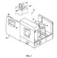
- FIG. 1is a perspective view of one embodiment of a semiconductor processing system in accordance with the present invention
- FIG. 2is a schematic cross-sectional view of one embodiment of the processing chambers shown above in FIG. 1 .
- FIG. 3is a schematic cross-sectional view of a substrate showing one possible mechanism of adsorption of a reductant over a substrate during sequential deposition.
- FIG. 4is a schematic cross-sectional view of a substrate showing one possible mechanism of adsorption of a refractory metal containing compound over the substrate after introduction of the reductant.
- FIG. 5is a graphical representation showing the concentration of gases present in a processing chamber, such as processing chamber as shown above in FIG. 2 .
- FIG. 6is a graphical representation showing the relationship between the number of ALD cycles and the thickness of a layer formed on a substrate employing sequential deposition techniques, in accordance with the present invention.
- FIG. 7is a graphical representation showing the relationship between the number of sequential deposition cycles and the resistivity of a layer formed on a substrate employing sequential deposition techniques, in accordance with the present invention.
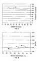
- FIG. 8is a graphical representation showing the relationship between the deposition rate of a layer formed on a substrate employing sequential deposition techniques and the temperature of the substrate.
- FIG. 9is a graphical representation showing the relationship between the resistivity of a layer formed on a substrate employing sequential deposition techniques and the temperature of the substrate, in accordance with the present invention.
- FIG. 10is a schematic cross-sectional view of one embodiment of a patterned substrate having a nucleation layer formed thereon employing sequential deposition techniques, in accordance with the present invention.
- FIG. 11is a schematic cross-sectional view of one embodiment of the substrate, shown above in FIG. 10 , with a refractory metal layer formed atop of the nucleation layer employing CVD, in accordance with the present invention.
- FIG. 12is a graphical representation showing the concentration of gases present in a processing chamber, such as the processing chamber as shown above in FIG. 2 , in accordance with an alternative embodiment of the present invention.
- FIG. 13is a graphical representation showing the concentration of gases present in a processing chamber, such as processing chamber as shown above in FIG. 2 , in accordance with an alternative embodiment of the present invention.
- FIG. 14is a graphical representation showing the fluorine content versus depth of a refractory metal layer formed on a substrate employing ALD, either Ar or N 2 being a carrier gas.
- FIG. 15is a graphical representation showing the fluorine content versus depth of a refractory metal layer formed on a substrate employing ALD with H 2 being a carrier gas.
- FIG. 16is a schematic cross-sectional view of one embodiment of a substrate shown above in FIGS. 3 and 4 upon which a layer of either PH 3 or B 2 H 6 is disposed between a substrate and a tungsten layer, in accordance with one embodiment of the present invention.
- FIG. 17is a graphical representation showing the concentration of gases present in a processing chamber, such as processing chamber as shown above in FIG. 2 , in accordance with one embodiment of the present invention.
- FIG. 18is a schematic cross-sectional view of one embodiment of a substrate shown above in FIGS. 3 and 4 in which a titanium-containing layer is deposited between a substrate and a layer of either PH 3 or B 2 H 6 , in accordance with the present invention.
- an exemplary wafer processing systemincludes one or more processing chambers 12 and 14 disposed in a common work area 16 surrounded by a wall 18 .
- Processing chambers 12 and 14are in data communication with a controller 22 that is connected to one or more monitors, shown as 24 and 26 .
- the monitorstypically display common information concerning the process associated with processing chambers 12 and 14 .
- One of the monitors 26is mounted on wall 18 , with the remaining monitor 24 being disposed in work area 16 .
- Operational control of processing chambers 12 and 14may be achieved by the use of a light pen, associated with one of the monitors 24 and 26 , to communicate with controller 22 .
- light pen 28is associated with monitor 24 and facilitates communication with controller 22 through monitor 24 .
- Light pen 39facilitates communication with controller 22 through monitor 26 .
- each of processing chambers 12 and 14includes a housing 30 having a base wall 32 , a cover 34 disposed opposite to base wall 32 , and a sidewall 36 extending therebetween.
- Housing 30defines a chamber 37
- a pedestal 38is disposed within processing chamber 37 to support a substrate 42 , such as a semiconductor wafer.
- Pedestal 38may be mounted to move between cover 34 and base wall 32 , using a displacement mechanism (not shown), but the position thereof is typically fixed.
- Supplies of processing gases 39 a , 39 b and 39 care in fluid communication with processing chamber 37 via a showerhead 40 . Regulation of the flow of gases from supplies 39 a , 39 b and 39 c is effectuated via flow valves 41 .
- substrate 42may be heated to a desired temperature prior to layer deposition via a heater embedded within pedestal 38 .
- pedestal 38may be resistively heated by applying an electric current from AC power supply 43 to heater element 44 .
- Substrate 42is, in turn, heated by pedestal 38 , and can be maintained within a desired process temperature range of, for example, about 20° C. to about 750° C.
- a temperature sensor 46such as a thermocouple, is also embedded in wafer support pedestal 38 to monitor the temperature of pedestal 38 in a conventional manner.
- the measured temperaturemay be used in a feedback loop to control the electrical current applied to heater element 44 by power supply 43 such that the substrate temperature can be maintained or controlled at a desired temperature that is suitable for the particular process application.
- pedestal 38may be heated using radiant heat (not shown).
- a vacuum pump 48is used to evacuate processing chamber 37 and to help maintain the proper gas flows and pressure inside processing chamber 37 .
- processing chambers 12 and 14may operate to deposit refractory metal layers on the substrate employing sequential deposition techniques.
- sequential deposition techniquesincludes atomic layer deposition (ALD).
- substrateincludes the substrate, such as semiconductor substrates and glass substrates, as well as layers formed thereover, such as dielectric layers (i.e., SiO 2 ) and barrier layers (i.e., titanium, titanium nitride and the like).
- FIG. 3is a schematic cross-sectional view of a substrate showing one possible mechanism of adsorption of a reductant over a substrate during sequential deposition.
- adsorptionor “adsorb” as used herein are defined to include chemisorption, physisorption, or any attractive and/or bonding forces which may be at work and/or which may contribute to the bonding, reaction, adherence, or occupation of a portion of an exposed surface of a substrate structure.
- a second batch of processing gas, “Bb y ,”is introduced into processing chamber 37 .
- the “a” ligand present on the substrate surfacereacts with the “b” ligand and “B” atom, releasing molecules, for example, “ab” and “aA,” which move away from substrate 42 and are subsequently pumped from processing chamber 37 .
- a surface comprising a layer of B compoundremains upon substrate 42 and exposed to processing chamber 37 , shown in FIG. 4 .
- the composition of the layer of B compoundmay be a monolayer or less of atoms typically formed employing ALD techniques. In other embodiments, more than a monolayer of B compound may be formed during each cycle.
- the layer of compound Bmay include a layer of multiple atoms (i.e. other atoms besides atoms of B).
- the first batch and/or the second batch of processing gasesmay include a mixture of process gases, each of which has atoms that would adhere to substrate 42 . The process proceeds cycle after cycle, until the desired thickness is achieved.
- the reductant “Aa x ”may comprise B 2 H 6 or PH 3 and the refractory metal containing compound, Bb y , may comprise WF 6 .
- Some possible reactionsare shown below in reference to chemical reaction (1) and chemical reaction (2).
- Other by-productsinclude but are not limited to H 2 , HF, F 2 .
- Other reactionsare also possible, such as decomposition reactions.
- other reductantsmay be used, such as SiH 4 .
- other tungsten containing gasesmay be used, such as W(CO) 6 .
- the purge gasincludes Ar, He, N 2 , H 2 , other suitable gases, and combinations thereof.
- One or more purge gasmay be used.
- FIG. 5is a graphical representation of one embodiment of gases present in a processing chamber utilizing two purge gases Ar and N 2 . Each of the processing gases was flowed into processing chamber 37 with a carrier gas, which in this example was one of the purge gases. WF 6 is introduced with Ar and B 2 H 6 is introduced with N 2 . It should be understood, however, that the purge gas may differ from the carrier gas, discussed more fully below.
- One cycle of the ALD technique in accordance with the present inventionincludes flowing the purge gas, N 2 , into processing chamber 37 during time t 1 , which is approximately about 0.01 to about 15 seconds before B 2 H 6 is flowed into processing chamber 37 .
- the processing gas B 2 H 6is flowed into processing chamber 37 for a time in the range of about 0.01 to about 15 seconds, along with a carrier gas, which in this example is N 2 .
- a carrier gaswhich in this example is N 2 .
- the flow of B 2 H 6terminates and the flow of N 2 continues during time t 3 for an additional time in the range of about 0.01 to about 15 seconds, purging the processing chamber of B 2 H 6 .
- processing chamber 37is pumped so as to remove most, if not all, gases.
- the carrier gas Aris introduced for a time in the range of about 0.01 to about 15 seconds during time t 5 , after which time the process gas WF 6 is introduced into processing chamber 37 , along with the carrier gas Ar during time t 6 .
- the time t 6lasts between about 0.01 to about 15 seconds.
- the flow of the processing gas WF 6 into processing chamber 37is terminated approximately about 0.01 to about 15 seconds after it commenced.
- the flow of Arcontinues for an additional time in the range of 0.01 to 15 seconds, during time t 7 .
- processing chamber 37is pumped so as to remove most, if not all, gases therein, during time t 8 .
- time t 8lasts approximately about 0 to about 30 seconds, thereby concluding one cycle of the sequential deposition technique, in accordance with the present invention.
- the cyclemay be repeated to deposit a tungsten layer to a desired thickness.
- the benefits of employing the sequential deposition techniqueare many fold, including flux-independence of layer formation that provides uniformity of deposition independent of the size of a substrate. For example, the measured difference of the layer uniformity and thickness measured between a 200 mm substrate and a 300 mm substrate deposited in the same chamber is negligible. This is due to the self-limiting characteristics of the sequential deposition techniques. Further, this technique contributes to improved step coverage over complex topography.
- the thickness of the layer Bmay be easily controlled while minimizing the resistance of the same by employing sequential deposition techniques.
- FIG. 6it is seen in the slope of line 50 that the thickness of the tungsten layer B is proportional to the number of cycles employed to form the same.
- the resistivity of the tungsten layeris relatively independent of the thickness of the layer, as shown by the slope of line 52 in FIG. 7 .
- the thickness of a refractory metal layermaybe easily controlled as a function of the cycling of the process gases introduced into the processing chamber with a negligible effect on the resistivity.
- FIG. 8is a graphical representation showing the relationship between the deposition rate of a layer formed on a substrate employing sequential deposition techniques and the temperature of the substrate. Control of the deposition rate was found to be dependent upon the temperature of substrate 42 . As shown by the slope of line 54 , increasing the temperature of substrate 42 increased the deposition rate of the tungsten layer B. The graph shows that less than a monolayer, a monolayer, or more than a monolayer of a tungsten layer may be formed depending on the substrate temperature utilized. For example, at 56 , the deposition rate is shown to be approximately 2 ⁇ /cycle at 250° C. However at point 58 the deposition rate is approximately 5 ⁇ /cycle at a temperate of 450° C.
- the resistivity of the tungsten layeris virtually independent of the layer thickness, as shown by the slope of curve 59 , shown in FIG. 9 .
- the deposition rate of the tungsten layermay be controlled as a function of temperature without compromising the resistivity of the same.
- a bulk deposition of the refractory metal layermay be included in the deposition process.
- the bulk deposition of the refractory metaloccurs after the nucleation layer is formed in a common processing chamber.
- nucleation of a tungsten layeroccurs in chamber 12 employing the sequential deposition techniques discussed above, with substrate 42 being heated in the range of about 200° C. to about 400° C., and processing chamber 37 being pressurized in the range of about 1 to about 10 Torr.
- a nucleation layer 60 of approximately about 120 to about 200 ⁇is formed on a patterned substrate 42 , shown in FIG. 10 .
- Nucleation layers of about 100 ⁇ or less, about 50 ⁇ or less, or about 25 ⁇ or lesshave also been found to be effective in providing good step coverage over apertures having an aspect ratio of about 6:1 or greater.
- substrate 42includes a barrier layer 61 and a patterned layer having a plurality of vias 63 .
- the nucleation layeris formed adjacent to the patterned layer covering vias 63 .
- forming nucleation layer 60employing ALD techniques provides good step coverage.
- sequential deposition techniquesmay be performed for both nucleation and bulk deposition.
- a bulk deposition of tungsten onto nucleation layer 60occurs using CVD techniques, while substrate 42 is disposed in the same processing chamber 12 , shown in FIG. 1 .
- the bulk depositionmay be performed using recipes well known in the art.
- a tungsten layer 65 providing a complete plug fillis achieved on the patterned layer with vias having aspect ratios of approximately 6:1, shown in FIG. 11 .
- a bifurcated deposition processmay be practiced in which nucleation of the refractory metal layer occurs in a chamber that is different from the chamber in which the remaining portion of the refractory metal layer is formed.
- nucleation of a tungsten layeroccurs in chamber 12 employing the sequential deposition techniques, such as ALD, discussed above.
- substrate 42is heated in the range of about 200° C. to about 400° C. and chamber 37 is pressurized in the range of about 1 to about 10 Torr.
- a nucleation layer 60 of approximately 120 to 200 ⁇is formed on a patterned substrate 42 , shown in FIG. 10 .
- substrate 42includes a barrier layer 61 and a patterned layer having a plurality of vias 63 .
- the nucleation layeris formed adjacent to the patterned layer covering the vias 63 .
- forming the nucleation layer 60employing sequential deposition techniques provides improved step coverage.
- sequential deposition techniquesare employed for bulk deposition of tungsten onto nucleation layer 60 occurs while substrate 42 is disposed in processing chamber 14 , shown in FIG. 1 .
- the bulk depositionmaybe performed using recipes disclosed herein.
- CVD techniquesare employed for bulk deposition of tungsten onto nucleation layer 60 occurs while substrate 42 is disposed in processing chamber 14 , shown in FIG. 1 .
- the bulk depositionmaybe performed using recipes well known in the art. Whether sequential deposition or CVD deposition techniques are employed, a tungsten layer 65 providing a complete plug fill is achieved on the patterned layer with vias having aspect ratios of approximately 6:1, shown in FIG. 11 . Implementing the bifurcated deposition process discussed above may decrease the time required to form a tungsten layer having improved characteristics. Utilizing CVD deposition techniques for bulk deposition may further increase throughput.
- the carrier gasmay differ from the purge gas, as shown in FIG. 12 .
- the purge gas, which is introduced at time intervals t 1 , t 3 , t 5 and t 7comprises Ar.
- the carrier gas, which is introduced at time intervals t 2 and t 6comprises of N 2 .
- the gases introduced into the processing chamberinclude a mixture of B 2 H 6 and N 2 , and a time interval t 6 , the gas mixture includes WF 6 and N 2 .
- the pump process during time intervals t 4 and t 8is identical to the pump process discussed above with respect to FIG. 5 .
- FIG. 12shows a time intervals t 1 , t 3 , t 5 and t 7 .
- the carrier gas, which is introduced at time intervals t 2 and t 6comprises of N 2 .
- the gases introduced into the processing chamberinclude a mixture of B 2 H 6 and N 2 , and a time interval t 6 , the gas mixture includes WF 6 and N
- the carrier gas during time intervals t 2 and t 6comprises H 2 , with the purge gas introduced at time intervals t 1 , t 3 , t 5 and t 7 comprising of Ar.
- the pump processes at time intervals t 4 and t 8are as discussed above, As a result, at time interval t 2 the gas mixture introduced into processing chamber 37 comprises of B 2 H 6 and H 2 , and WF 6 , and H 2 at time interval t 6 .
- An advantage realized by employing the H 2 carrier gasis that the stability of the tungsten layer B may be improved. Specifically, by comparing curve 66 in FIG. 14 with curve 68 in FIG. 15 , it is seen that the concentration of fluorine in the nucleation layer 60 , shown in FIG. 10 , is much less when H 2 is employed as the carrier gas, as compared with use of N 2 or Ar as a carrier gas.
- the apex and nadir of curve 66show that the fluorine concentration reaches levels in excess of 1 ⁇ 10 21 atoms per cubic centimeter and only as low as just below 1 ⁇ 10 19 atoms per cubic centimeter.
- Curve 68shows that the fluorine concentration is well below 1 ⁇ 10 21 atoms per cubic centimeter at the apex and well below 1 ⁇ 10 17 atoms per cubic centimeter at the nadir.
- employing H 2 as the carrier gasprovides a much more stable film, i.e., the probability of fluorine diffusing into the substrate, or adjacent layer is reduced.
- the stability of the nucleation layer, as well as the resistivity of the same,may be controlled as a function of the carrier gas employed. This is also true when a refractory metal layer is deposited entirely employing ALD techniques, i.e., without using other deposition techniques, such as CVD.
- adsorbing a layer 70 , shown in FIG. 16 , of either PH 3 or B 2 H 6 prior to introduction of the tungsten containing compoundforms a tungsten layer 72 with reduced fluorine content, improved step coverage, and improved resistivity.
- the improved characteristics of the tungsten filmare believed to be attributable to the chemical affinity between the PH 3 or B 2 H 6 layer and the WF 6 layer. This provides better surface mobility of the adsorbed chemical species and better reduction of WF 6 at the nucleation stage of the tungsten layer. This has proven beneficial when depositing a tungsten layer adjacent to a titanium containing adhesion layer formed from titanium, Ti, or titanium nitride, TiN.
- Layer 70is preferably a monolayer, but in other embodiments may be less than or more than a monolayer.
- Layer 70 in the film stack, shown in FIG. 16shows the formation of the tungsten layer 72 . It is understood that layer 70 may or may not be consumed during formation of the tungsten layer 72 .
- a plurality of layers 70 and tungsten layers 72may be deposited to form a tungsten layer to a desired thickness.
- layer 70is deposited on substrate 74 that includes a wafer 76 that may be formed from any material suitable for semiconductor processing, such as silicon.
- a wafer 76may be formed from any material suitable for semiconductor processing, such as silicon.
- One or more layers, shown as layer 74may be present on wafer 76 .
- Layer 78may be formed from any suitable material, included dielectric or conductive materials.
- Layer 78includes a void 80 , exposing a region 82 of wafer 76 .
- FIG. 18is a detailed cross-sectional view of a substrate in which a titanium-containing adhesion layer is formed between a substrate and a layer of either PH 3 or B 2 H 6 during the fabrication of a W layer adjacent to the titanium-containing adhesion layer.
- the titanium-containing adhesion layermay be formed employing standard CVD techniques.
- the titanium-containing adhesion layeris formed employing sequential deposition techniques.
- processing gas Aa xis selected from the group including H 2 , B 2 H 6 , SiH 4 and NH 3 .
- Processing gas Bb yis a titanium-containing gas selected from the group that includes TDMAT, TDEAT and TiCl 4 .
- Ar and N 2 purge gasesare preferably employed, although other purge gas may be used.
- each of the processing gasesis flowed into processing chamber 37 with a carrier gas, which in this example, is one of the purge gases. It should be understood, however, that the purge gas may differ from the carrier gas, discussed more fully below.
- One cycle of the sequential deposition techniqueincludes flowing a purge gas into processing chamber 37 during time t 1 before the titanium-containing gas is flowed into processing chamber 37 .
- time t 2the titanium-containing processing gas is flowed into the processing chamber 37 , along with a carrier gas.
- the flow of titanium-containing gasterminates and the flow of the carrier gas continues during time t 3 , purging the processing chamber of the titanium-containing processing gas.
- the processing chamber 37is pumped so as to remove all gases.
- a carrier gasis introduced during time t 5 , after which time the reducing process gas is introduced into the processing chamber 37 along with the carrier gas, during time t 6 .
- the flow of the reducing process gas into processing chamber 37is subsequently terminated.
- the flow of carrier gascontinues, during time t 7 .
- processing chamber 37is pumped so as to remove all gases therein, during time t 8 , thereby concluding one cycle of the sequential deposition technique in accordance with the present invention.
- the aforementioned cycleis repeated multiple times until titanium-containing layer reaches a desired thickness.
- layer 86in this example formed from PH 3 or B 2 H 6 , is deposited adjacent thereto employing sequential deposition techniques, as discussed above.
- a layer of tungsten 88shown in FIG. 18 , is disposed adjacent to layer 86 using the sequential deposition technique or standard CVD techniques, both of which are discussed above.
- Layer 86is preferably a monolayer, but in other embodiments may be less than or more than a monolayer.
- Layer 86 in the film stack, shown in FIG. 18shows the formation of the tungsten layer 88 . It is understood that layer 86 may or may not be consumed during formation of the tungsten layer 88 . It is also understood that a plurality of layers 86 and tungsten layers 66 may be deposited to form a tungsten layer to a desired thickness. If desired, a copper layer maybe deposited atop of tungsten layer 88 . In this manner, tungsten may function as a barrier layer.
- controller 22includes a central processing unit (CPU) 90 , a volatile memory, such as a random access memory (RAM) 92 and permanent storage media, such as a floppy disk drive for use with a floppy diskette, or hard disk drive 94 .
- the computer program codecan be written in any conventional computer readable programming language; for example, 68000 assembly language, C, C++, Pascal, Fortran and the like. Suitable program code is entered into a single file, or multiple files, using a conventional text editor and stored or embodied in a computer-readable medium, such as hard disk drive 94 .
- the codeis compiled and the resultant compiler code is then linked with an object code of precompiled Windows® library routines.
- the system userinvokes the object code, causing the CPU 90 to load the code in RAM 92 .
- the CPU 90then reads and executes the code to perform the tasks identified in the program.
Landscapes
- Chemical & Material Sciences (AREA)
- Engineering & Computer Science (AREA)
- General Chemical & Material Sciences (AREA)
- Chemical Kinetics & Catalysis (AREA)
- Physics & Mathematics (AREA)
- Manufacturing & Machinery (AREA)
- Metallurgy (AREA)
- Organic Chemistry (AREA)
- Materials Engineering (AREA)
- Condensed Matter Physics & Semiconductors (AREA)
- General Physics & Mathematics (AREA)
- Mechanical Engineering (AREA)
- Computer Hardware Design (AREA)
- Microelectronics & Electronic Packaging (AREA)
- Power Engineering (AREA)
- Chemical Vapour Deposition (AREA)
- Electrodes Of Semiconductors (AREA)
- Internal Circuitry In Semiconductor Integrated Circuit Devices (AREA)
Abstract
Description
This application claims benefit of U.S. Provisional Patent Application Ser. No. 60/305,765, filed Jul. 16, 2001, which is herein incorporated by reference.
1. Field of the Invention
Embodiments of the invention relate to the processing of semiconductor substrates. More particularly, embodiments of the invention relate to improvements in the process of depositing refractory metal layers on semiconductor substrates.
2. Description of the Related Art
The semiconductor processing industry continues to strive for larger production yields while increasing the uniformity of layers deposited on substrates having larger surface areas. These same factors in combination with new materials also provide higher density of circuits per unit area of the substrate. As circuit density increases, the need for greater uniformity and process control regarding layer thickness rises. As a result, various technologies have been developed to deposit layers on substrates in a cost-effective manner, while maintaining control over the characteristics of the layer. Chemical Vapor Deposition (CVD) is one of the most common deposition processes employed for depositing layers on a substrate. CVD is a flux-dependent deposition technique that requires precise control of the substrate temperature and precursors introduced into the processing chamber in order to produce a desired layer of uniform thickness. These requirements become more critical as substrate size increases (e.g., from 200 mm diameter substrates to 300 mm substrates), creating a need for more complexity in chamber design and gas flow technique to maintain adequate uniformity.
A variant of CVD that demonstrates superior step coverage compared to CVD, is Atomic Layer Deposition (ALD). ALD is based upon Atomic Layer Epitaxy (ALE) that was employed originally to fabricate electroluminescent displays. ALD employs chemisorption to deposit a saturated monolayer of reactive precursor molecules on a substrate surface. This is achieved by alternatingly pulsing an appropriate reactive precursor into a deposition chamber. Each injection of a reactive precursor is separated by an inert gas purge to provide an adsorbed atomic layer to previously deposited layers to form a uniform layer on the substrate. The cycle is repeated to form the layer to a desired thickness. A drawback with ALD techniques is that the deposition rate is much lower than typical CVD techniques by at least one order of magnitude.
Formation of film layers at a high deposition rate while providing adequate step coverage are conflicting characteristics often necessitating sacrificing one to obtain the other. This conflict is true particularly when refractory metal layers are deposited to cover apertures or vias during formation of contacts that interconnect adjacent metallic layers separated by dielectric layers. Historically, CVD techniques have been employed to deposit conductive material such as refractory metals in order to inexpensively and quickly fill vias. Due to the increasing density of semiconductor circuitry, tungsten has been used based upon superior step coverage to fill these high aspect ratio structures. As a result, deposition of tungsten employing CVD techniques enjoys wide application in semiconductor processing due to the high throughput of the process and good step coverage.
Depositing tungsten by traditional CVD methods, however, is attendant with several disadvantages. For example, blanket deposition of a tungsten layer on a semiconductor wafer is time-consuming at temperatures below 400° C. The deposition rate of tungsten may be improved by increasing the deposition temperature between approximately 500° C. to 550° C.; however, temperatures in this higher range may compromise the structural and operational integrity of the underlying portions of the integrated circuit being formed. Use of tungsten has also complicated photolithography steps during the manufacturing process as it results in a relatively rough surface having a reflectivity of 20% or less than that of a silicon substrate. Finally, tungsten has, proven difficult to deposit uniformly. Variance in film thickness of greater than 1% has been shown, thereby causing poor control of the resistivity of the layer. Several prior attempts to overcome the aforementioned drawbacks have been attempted.
For example, in U.S. Pat. No. 5,028,565 to Chang et al., which is assigned to the assignee of the present invention, a method is disclosed to improve, inter alia, uniformity of tungsten layers by varying the deposition chemistry. The method includes, in pertinent part, formation of a nucleation layer over an intermediate barrier layer before depositing the tungsten layer via bulk deposition. The nucleation layer is formed from a gaseous mixture of tungsten hexafluoride, hydrogen, silane and argon. The nucleation layer is described as providing a layer of growth sites to promote uniform deposition of a tungsten layer thereon. The benefits provided by the nucleation layer are described as being dependent upon the barrier layer present. For example, were the barrier layer formed from titanium nitride, the tungsten layer's thickness uniformity is improved as much as 15%. Were the barrier layer formed from sputtered tungsten or sputtered titanium tungsten, the benefits provided by the nucleation layer are not as pronounced.
A need exists, therefore, to provide techniques to improve the characteristics of refractory metal layers deposited on semiconductor substrates.
A method and system to form a refractory metal layer over a substrate includes introduction of a reductant, such as PH3or B2H6, followed by introduction of a tungsten containing compound, such as WF6, to form a tungsten layer. It is believed that the reductant reduces the fluorine content of the tungsten layer while improving the step coverage and resistivity of the tungsten layer. It is believed that the improved characteristics of the tungsten film are attributable to the chemical affinity between the reductants and the tungsten containing compound. The chemical affinity provides better surface mobility of the adsorbed chemical species and better reduction of WF6at the nucleation stage of the tungsten layer.
The method can further include sequentially introducing a reductant, such as PH3or B2H6, and a tungsten containing compound to deposit a tungsten layer. The formed tungsten layer can be used as a nucleation layer followed by bulk deposition of a tungsten layer utilizing standard CVD techniques. Alternatively, the formed tungsten layer can be used to fill an aperture.
Referring toFIG. 1 , an exemplary wafer processing system includes one ormore processing chambers common work area 16 surrounded by awall 18.Processing chambers controller 22 that is connected to one or more monitors, shown as24 and26. The monitors typically display common information concerning the process associated withprocessing chambers monitors 26 is mounted onwall 18, with the remainingmonitor 24 being disposed inwork area 16. Operational control ofprocessing chambers monitors controller 22. For example,light pen 28 is associated withmonitor 24 and facilitates communication withcontroller 22 throughmonitor 24.Light pen 39 facilitates communication withcontroller 22 throughmonitor 26.
Referring both toFIGS. 1 and 2 , each of processingchambers housing 30 having abase wall 32, acover 34 disposed opposite tobase wall 32, and asidewall 36 extending therebetween.Housing 30 defines achamber 37, and apedestal 38 is disposed withinprocessing chamber 37 to support asubstrate 42, such as a semiconductor wafer.Pedestal 38 may be mounted to move betweencover 34 andbase wall 32, using a displacement mechanism (not shown), but the position thereof is typically fixed. Supplies of processing gases39a,39band39care in fluid communication withprocessing chamber 37 via ashowerhead 40. Regulation of the flow of gases from supplies39a,39band39cis effectuated viaflow valves 41.
Depending on the specific process,substrate 42 may be heated to a desired temperature prior to layer deposition via a heater embedded withinpedestal 38. For example,pedestal 38 may be resistively heated by applying an electric current fromAC power supply 43 toheater element 44.Substrate 42 is, in turn, heated bypedestal 38, and can be maintained within a desired process temperature range of, for example, about 20° C. to about 750° C.A temperature sensor 46, such as a thermocouple, is also embedded inwafer support pedestal 38 to monitor the temperature ofpedestal 38 in a conventional manner. For example, the measured temperature may be used in a feedback loop to control the electrical current applied toheater element 44 bypower supply 43 such that the substrate temperature can be maintained or controlled at a desired temperature that is suitable for the particular process application. Optionally,pedestal 38 may be heated using radiant heat (not shown). Avacuum pump 48 is used to evacuateprocessing chamber 37 and to help maintain the proper gas flows and pressure inside processingchamber 37.
Referring toFIGS. 1 and 2 , one or both ofprocessing chambers
Not wishing to be bound by theory,FIG. 3 is a schematic cross-sectional view of a substrate showing one possible mechanism of adsorption of a reductant over a substrate during sequential deposition. The terms “adsorption” or “adsorb” as used herein are defined to include chemisorption, physisorption, or any attractive and/or bonding forces which may be at work and/or which may contribute to the bonding, reaction, adherence, or occupation of a portion of an exposed surface of a substrate structure. During the sequential deposition technique, in accordance with the present invention, a batch of a first processing gas, in this case “Aax,” results in a layer of “A” being deposited onsubstrate 42 having a surface of ligand “a” exposed to processingchamber 37. Layer “A” may be a monolayer, more than a monolayer, or less than a monolayer. Thereafter, a purge gas enters processingchamber 37 to purge gas “Aax,” which has not been incorporated into the layer of A.FIG. 4 is a schematic cross-sectional view of a substrate showing one possible mechanism of adsorption of a refractory metal containing compound over the substrate after introduction of the reductant. After purging gas “Aax” from processingchamber 37, a second batch of processing gas, “Bby,” is introduced intoprocessing chamber 37. The “a” ligand present on the substrate surface reacts with the “b” ligand and “B” atom, releasing molecules, for example, “ab” and “aA,” which move away fromsubstrate 42 and are subsequently pumped from processingchamber 37. In this manner, a surface comprising a layer of B compound remains uponsubstrate 42 and exposed to processingchamber 37, shown in FIG.4. The composition of the layer of B compound may be a monolayer or less of atoms typically formed employing ALD techniques. In other embodiments, more than a monolayer of B compound may be formed during each cycle. Alternatively, the layer of compound B may include a layer of multiple atoms (i.e. other atoms besides atoms of B). In such a case, the first batch and/or the second batch of processing gases may include a mixture of process gases, each of which has atoms that would adhere tosubstrate 42. The process proceeds cycle after cycle, until the desired thickness is achieved.
Referring to bothFIGS. 3 and 4 , although any type of processing gas may be employed, in the present example, the reductant “Aax” may comprise B2H6or PH3and the refractory metal containing compound, Bby, may comprise WF6. Some possible reactions are shown below in reference to chemical reaction (1) and chemical reaction (2).
B2H6(g)+WF6(g)→W(s)+2BF3(g) (1)
PH3(g)+WF6(g)→W(s)+PF3(g) (2)
Other by-products include but are not limited to H2, HF, F2. Other reactions are also possible, such as decomposition reactions. In other embodiments, other reductants may be used, such as SiH4. Similarly, in other embodiments, other tungsten containing gases may be used, such as W(CO)6.
The purge gas includes Ar, He, N2, H2, other suitable gases, and combinations thereof. One or more purge gas may be used.FIG. 5 is a graphical representation of one embodiment of gases present in a processing chamber utilizing two purge gases Ar and N2. Each of the processing gases was flowed intoprocessing chamber 37 with a carrier gas, which in this example was one of the purge gases. WF6is introduced with Ar and B2H6is introduced with N2. It should be understood, however, that the purge gas may differ from the carrier gas, discussed more fully below. One cycle of the ALD technique in accordance with the present invention includes flowing the purge gas, N2, intoprocessing chamber 37 during time t1, which is approximately about 0.01 to about 15 seconds before B2H6is flowed intoprocessing chamber 37. During time t2, the processing gas B2H6is flowed intoprocessing chamber 37 for a time in the range of about 0.01 to about 15 seconds, along with a carrier gas, which in this example is N2. After about 0.01 to about 15 seconds have lapsed, the flow of B2H6terminates and the flow of N2continues during time t3for an additional time in the range of about 0.01 to about 15 seconds, purging the processing chamber of B2H6. During time t4which lasts approximately about 0 to about 30 seconds, processingchamber 37 is pumped so as to remove most, if not all, gases. After pumping ofprocess chamber 37, the carrier gas Ar is introduced for a time in the range of about 0.01 to about 15 seconds during time t5, after which time the process gas WF6is introduced intoprocessing chamber 37, along with the carrier gas Ar during time t6. The time t6lasts between about 0.01 to about 15 seconds. The flow of the processing gas WF6intoprocessing chamber 37 is terminated approximately about 0.01 to about 15 seconds after it commenced. After the flow of WF6intoprocessing chamber 37 terminates, the flow of Ar continues for an additional time in the range of 0.01 to 15 seconds, during time t7. Thereafter, processingchamber 37 is pumped so as to remove most, if not all, gases therein, during time t8. As before, time t8lasts approximately about 0 to about 30 seconds, thereby concluding one cycle of the sequential deposition technique, in accordance with the present invention. The cycle may be repeated to deposit a tungsten layer to a desired thickness.
The benefits of employing the sequential deposition technique are many fold, including flux-independence of layer formation that provides uniformity of deposition independent of the size of a substrate. For example, the measured difference of the layer uniformity and thickness measured between a 200 mm substrate and a 300 mm substrate deposited in the same chamber is negligible. This is due to the self-limiting characteristics of the sequential deposition techniques. Further, this technique contributes to improved step coverage over complex topography.
In addition, the thickness of the layer B, shown inFIG. 4 , may be easily controlled while minimizing the resistance of the same by employing sequential deposition techniques. With reference toFIG. 6 , it is seen in the slope ofline 50 that the thickness of the tungsten layer B is proportional to the number of cycles employed to form the same. The resistivity of the tungsten layer, however, is relatively independent of the thickness of the layer, as shown by the slope ofline 52 in FIG.7. Thus, employing sequential deposition techniques, the thickness of a refractory metal layer maybe easily controlled as a function of the cycling of the process gases introduced into the processing chamber with a negligible effect on the resistivity.
To that end, a bulk deposition of the refractory metal layer may be included in the deposition process. Typically, the bulk deposition of the refractory metal occurs after the nucleation layer is formed in a common processing chamber. Specifically, in the present example, nucleation of a tungsten layer occurs inchamber 12 employing the sequential deposition techniques discussed above, withsubstrate 42 being heated in the range of about 200° C. to about 400° C., andprocessing chamber 37 being pressurized in the range of about 1 to about 10 Torr. Anucleation layer 60 of approximately about 120 to about 200 Å is formed on a patternedsubstrate 42, shown in FIG.10. Nucleation layers of about 100 Å or less, about 50 Å or less, or about 25 Å or less have also been found to be effective in providing good step coverage over apertures having an aspect ratio of about 6:1 or greater. As shown,substrate 42 includes abarrier layer 61 and a patterned layer having a plurality ofvias 63. The nucleation layer is formed adjacent to the patternedlayer covering vias 63. As shown, formingnucleation layer 60 employing ALD techniques provides good step coverage. In another embodiment, sequential deposition techniques may be performed for both nucleation and bulk deposition. In still another embodiment, to decrease the time required to form a complete layer of tungsten, a bulk deposition of tungsten ontonucleation layer 60 occurs using CVD techniques, whilesubstrate 42 is disposed in thesame processing chamber 12, shown in FIG.1. The bulk deposition may be performed using recipes well known in the art. In this manner, atungsten layer 65 providing a complete plug fill is achieved on the patterned layer with vias having aspect ratios of approximately 6:1, shown in FIG.11.
In an alternative embodiment, a bifurcated deposition process may be practiced in which nucleation of the refractory metal layer occurs in a chamber that is different from the chamber in which the remaining portion of the refractory metal layer is formed. Specifically, in the present example, nucleation of a tungsten layer occurs inchamber 12 employing the sequential deposition techniques, such as ALD, discussed above. To that end,substrate 42 is heated in the range of about 200° C. to about 400° C. andchamber 37 is pressurized in the range of about 1 to about 10 Torr. Anucleation layer 60 of approximately 120 to 200 Å is formed on a patternedsubstrate 42, shown in FIG.10. Nucleation layers of about 100 Å or less, about 50 Å or less, or about 25 Å or less have also been found to be effective in providing good step coverage over apertures having an aspect ratio of about 6:1 or greater. As shown,substrate 42 includes abarrier layer 61 and a patterned layer having a plurality ofvias 63. The nucleation layer is formed adjacent to the patterned layer covering thevias 63. As shown, forming thenucleation layer 60 employing sequential deposition techniques provides improved step coverage.
In one embodiment, sequential deposition techniques are employed for bulk deposition of tungsten ontonucleation layer 60 occurs whilesubstrate 42 is disposed in processingchamber 14, shown in FIG.1. The bulk deposition maybe performed using recipes disclosed herein. In another embodiment, CVD techniques are employed for bulk deposition of tungsten ontonucleation layer 60 occurs whilesubstrate 42 is disposed in processingchamber 14, shown in FIG.1. The bulk deposition maybe performed using recipes well known in the art. Whether sequential deposition or CVD deposition techniques are employed, atungsten layer 65 providing a complete plug fill is achieved on the patterned layer with vias having aspect ratios of approximately 6:1, shown in FIG.11. Implementing the bifurcated deposition process discussed above may decrease the time required to form a tungsten layer having improved characteristics. Utilizing CVD deposition techniques for bulk deposition may further increase throughput.
As mentioned above, in an alternate embodiment of the present invention, the carrier gas may differ from the purge gas, as shown in FIG.12. The purge gas, which is introduced at time intervals t1, t3, t5and t7comprises Ar. The carrier gas, which is introduced at time intervals t2and t6, comprises of N2. Thus, at time interval t2the gases introduced into the processing chamber include a mixture of B2H6and N2, and a time interval t6, the gas mixture includes WF6and N2. The pump process during time intervals t4and t8is identical to the pump process discussed above with respect to FIG.5. In yet another embodiment, shown inFIG. 13 , the carrier gas during time intervals t2and t6comprises H2, with the purge gas introduced at time intervals t1, t3, t5and t7comprising of Ar. The pump processes at time intervals t4and t8are as discussed above, As a result, at time interval t2the gas mixture introduced intoprocessing chamber 37 comprises of B2H6and H2, and WF6, and H2at time interval t6.
An advantage realized by employing the H2carrier gas is that the stability of the tungsten layer B may be improved. Specifically, by comparingcurve 66 inFIG. 14 withcurve 68 inFIG. 15 , it is seen that the concentration of fluorine in thenucleation layer 60, shown inFIG. 10 , is much less when H2is employed as the carrier gas, as compared with use of N2or Ar as a carrier gas.
Referring to bothFIGS. 14 and 15 , the apex and nadir ofcurve 66 show that the fluorine concentration reaches levels in excess of 1×10²¹atoms per cubic centimeter and only as low as just below 1×10¹⁹atoms per cubic centimeter.Curve 68, however, shows that the fluorine concentration is well below 1×10²¹atoms per cubic centimeter at the apex and well below 1×10¹⁷atoms per cubic centimeter at the nadir. Thus, employing H2as the carrier gas provides a much more stable film, i.e., the probability of fluorine diffusing into the substrate, or adjacent layer is reduced. This also reduces the resistance of the refractory metal layer by avoiding the formation of a metal fluoride that may result from the increased fluorine concentration. Thus, the stability of the nucleation layer, as well as the resistivity of the same, may be controlled as a function of the carrier gas employed. This is also true when a refractory metal layer is deposited entirely employing ALD techniques, i.e., without using other deposition techniques, such as CVD.
In addition, adsorbing alayer 70, shown inFIG. 16 , of either PH3or B2H6prior to introduction of the tungsten containing compound forms atungsten layer 72 with reduced fluorine content, improved step coverage, and improved resistivity. This was found to be the case where the tungsten containing compound is introduced over a layer of PH3or B2H6employing sequential deposition techniques or employing standard CVD techniques using either tungsten hexafluoride, WF6, and silane, SiH4, or tungsten hexafluoride, WF6, and molecular hydrogen, H2, chemistries. The improved characteristics of the tungsten film are believed to be attributable to the chemical affinity between the PH3or B2H6layer and the WF6layer. This provides better surface mobility of the adsorbed chemical species and better reduction of WF6at the nucleation stage of the tungsten layer. This has proven beneficial when depositing a tungsten layer adjacent to a titanium containing adhesion layer formed from titanium, Ti, or titanium nitride, TiN.Layer 70 is preferably a monolayer, but in other embodiments may be less than or more than a monolayer.Layer 70 in the film stack, shown inFIG. 16 , shows the formation of thetungsten layer 72. It is understood thatlayer 70 may or may not be consumed during formation of thetungsten layer 72. It is also understood that a plurality oflayers 70 andtungsten layers 72 may be deposited to form a tungsten layer to a desired thickness. As shown,layer 70 is deposited onsubstrate 74 that includes awafer 76 that may be formed from any material suitable for semiconductor processing, such as silicon. One or more layers, shown aslayer 74, may be present onwafer 76.Layer 78 may be formed from any suitable material, included dielectric or conductive materials.Layer 78 includes a void80, exposing a region82 ofwafer 76.
Referring toFIGS. 2 and 17 , each of the processing gases is flowed intoprocessing chamber 37 with a carrier gas, which in this example, is one of the purge gases. It should be understood, however, that the purge gas may differ from the carrier gas, discussed more fully below. One cycle of the sequential deposition technique, in accordance with the present invention, includes flowing a purge gas into processingchamber 37 during time t1before the titanium-containing gas is flowed intoprocessing chamber 37. During time t2, the titanium-containing processing gas is flowed into theprocessing chamber 37, along with a carrier gas. After t2has lapsed, the flow of titanium-containing gas terminates and the flow of the carrier gas continues during time t3, purging the processing chamber of the titanium-containing processing gas. During time t4, theprocessing chamber 37 is pumped so as to remove all gases. After pumping ofprocess chamber 37, a carrier gas is introduced during time t5, after which time the reducing process gas is introduced into theprocessing chamber 37 along with the carrier gas, during time t6. The flow of the reducing process gas into processingchamber 37 is subsequently terminated. After the flow of reducing process gas into processingchamber 37 terminates, the flow of carrier gas continues, during time t7. Thereafter, processingchamber 37 is pumped so as to remove all gases therein, during time t8, thereby concluding one cycle of the sequential deposition technique in accordance with the present invention. The aforementioned cycle is repeated multiple times until titanium-containing layer reaches a desired thickness. For example, in reference toFIG. 18 , afterTiN layer 84 reaches a desired thickness,layer 86, in this example formed from PH3or B2H6, is deposited adjacent thereto employing sequential deposition techniques, as discussed above. Thereafter, a layer of tungsten88, shown inFIG. 18 , is disposed adjacent to layer86 using the sequential deposition technique or standard CVD techniques, both of which are discussed above.Layer 86 is preferably a monolayer, but in other embodiments may be less than or more than a monolayer.Layer 86 in the film stack, shown inFIG. 18 , shows the formation of the tungsten layer88. It is understood thatlayer 86 may or may not be consumed during formation of the tungsten layer88. It is also understood that a plurality oflayers 86 andtungsten layers 66 may be deposited to form a tungsten layer to a desired thickness. If desired, a copper layer maybe deposited atop of tungsten layer88. In this manner, tungsten may function as a barrier layer.
Referring again toFIG. 2 , the process for depositing the tungsten layer may be controlled using a computer program product that is executed bycontroller 22. To that end,controller 22 includes a central processing unit (CPU)90, a volatile memory, such as a random access memory (RAM)92 and permanent storage media, such as a floppy disk drive for use with a floppy diskette, orhard disk drive 94. The computer program code can be written in any conventional computer readable programming language; for example, 68000 assembly language, C, C++, Pascal, Fortran and the like. Suitable program code is entered into a single file, or multiple files, using a conventional text editor and stored or embodied in a computer-readable medium, such ashard disk drive 94. If the entered code text is in a high level language, the code is compiled and the resultant compiler code is then linked with an object code of precompiled Windows® library routines. To execute the linked and compiled object code, the system user invokes the object code, causing theCPU 90 to load the code inRAM 92. TheCPU 90 then reads and executes the code to perform the tasks identified in the program.
Although the invention has been described in terms of specific embodiments, one skilled in the art will recognize that various changes to the reaction conditions, i.e., temperature, pressure, film thickness and the like can be substituted and are meant to be included herein. Additionally, while the bifurcated deposition process has been described as occurring in a common system, the bulk deposition may occur in a processing chamber of a mainframe deposition system that is different from the mainframe deposition system in which the processing chamber is located that is employed to deposit the nucleation layer. Finally, other refractory metals may be deposited, in addition to tungsten, and other deposition techniques may be employed in lieu of CVD. For example, physical vapor deposition (PVD) techniques, or a combination of both CVD and PVD techniques may be employed. The scope of the invention should not be based upon the foregoing description. Rather, the scope of the invention should be determined based upon the claims recited herein, including the full scope of equivalents thereof.
Claims (22)
1. A method of sequential deposition of a tungsten nucleation layer and a bulk tungsten layer over a substrate in a processing chamber, comprising:
introducing a pulse of reducing gas comprising phosphine;
introducing a tungsten containing compound to form the nucleation layer; and:
forming the bulk tungsten layer over the tungsten nucleation layer.
2. A method of depositing a tungsten layer over a substrate in a processing chamber, comprising:
adsorbing a layer over the substrate comprising phosphine; and
introducing a tungsten containing compound to form a tungsten layer, wherein introducing the tungsten containing compound comprises introducing the tungsten containing compound in a sequential deposition technique.
3. A method of forming a tungsten layer over a substrate in a processing chamber, comprising:
presoaking the substrate with phosphine to form a presoak layer over the substrate; and
forming a tungsten layer over the presoak layer by sequentially introducing pulses of a tungsten-containing compound and pulses of a reductant.
4. The method ofclaim 3 , wherein the substrate is presoaked and the tungsten layer is formed in the same processing chamber.
5. The method ofclaim 3 , wherein the reductant is selected from the group consisting of hydrogen, silane, diborane and phosphine.
6. The method ofclaim 3 , further comprising introducing a purge gas at least partially between the pulses of the reductant and the pulses of the tungsten containing compound.
7. The method ofclaim 3 , wherein the substrate comprises a titanium-containing layer and the presoak layer is formed over the titanium-containing layer.
8. The method ofclaim 3 , wherein the tungsten layer is a tungsten nucleation layer.
9. The method ofclaim 8 , further comprising forming a bulk tungsten layer over the tungsten nucleation layer.
10. A method of forming a tungsten layer on a substrate in a processing chamber, comprising:
presoaking the substrate with phosphine to form a presoak layer on the substrate; and
forming the tungsten layer on the presoak layer by an ALD process comprising:
flowing a tungsten-containing compound into the processing chamber;
chemisorbing the tungsten-containing compound to the presoak layer;
purging the processing chamber with a purge gas;
flowing a reductant selected from the group consisting of hydrogen, silane, diborane and phosphine into the processing chamber; and
purging the processing chamber with the purge gas.
11. The method ofclaim 10 , wherein the substrate is presoaked and the tungsten layer is formed in the same processing chamber.
12. The method ofclaim 10 , wherein the reductant is diborane.
13. The method ofclaim 10 , wherein the purge gas is selected from the group consisting of Ar, He, H2, N2and combinations thereof.
14. The method ofclaim 10 , wherein the substrate comprises a titanium-containing layer and the presoak layer is formed over the titanium-containing layer.
15. The method ofclaim 10 , wherein the tungsten layer is a tungsten nucleation layer.
16. The method ofclaim 15 , further comprising forming a bulk tungsten layer over the tungsten nucleation layer.
17. The method ofclaim 8 , wherein the bulk tungsten layer is deposited by a process selected from the group consisting of ALD, CVD, PVD or combinations thereof.
18. The method ofclaim 16 , wherein the bulk tungsten layer is deposited by a process selected from the group consisting of ALD, CVD, PVD or combinations thereof.
19. A method of forming a tungsten layer on a substrate in a processing chamber, comprising:
sequentially pulsing a tungsten containing compound and phosphine by an ALD process to deposit a nucleation tungsten layer; and
forming a bulk tungsten layer over the nucleation tungsten layer.
20. The method ofclaim 19 , wherein the ALD process further comprises a purge gas selected from the group consisting of Ar, He, H2, N2and combinations thereof.
21. The method ofclaim 20 , wherein the nucleation tungsten layer is deposited on a barrier layer selected from the group consisting of titanium, titanium nitride and combinations thereof.
22. The method ofclaim 21 , wherein the bulk tungsten layer is deposited by a process selected from the group consisting of ALD, CVD, PVD or combinations thereof.
Priority Applications (6)
| Application Number | Priority Date | Filing Date | Title |
|---|---|---|---|
| US10/196,514US6936538B2 (en) | 2001-07-16 | 2002-07-15 | Method and apparatus for depositing tungsten after surface treatment to improve film characteristics |
| US11/038,592US7405158B2 (en) | 2000-06-28 | 2005-01-19 | Methods for depositing tungsten layers employing atomic layer deposition techniques |
| US11/130,515US7238552B2 (en) | 2001-07-16 | 2005-05-17 | Method and apparatus for depositing tungsten after surface treatment to improve film characteristics |
| US11/768,647US7749815B2 (en) | 2001-07-16 | 2007-06-26 | Methods for depositing tungsten after surface treatment |
| US12/179,002US7745333B2 (en) | 2000-06-28 | 2008-07-24 | Methods for depositing tungsten layers employing atomic layer deposition techniques |
| US12/239,046US7732327B2 (en) | 2000-06-28 | 2008-09-26 | Vapor deposition of tungsten materials |
Applications Claiming Priority (2)
| Application Number | Priority Date | Filing Date | Title |
|---|---|---|---|
| US30576501P | 2001-07-16 | 2001-07-16 | |
| US10/196,514US6936538B2 (en) | 2001-07-16 | 2002-07-15 | Method and apparatus for depositing tungsten after surface treatment to improve film characteristics |
Related Child Applications (3)
| Application Number | Title | Priority Date | Filing Date |
|---|---|---|---|
| US09/605,593Continuation-In-PartUS6551929B1 (en) | 2000-06-28 | 2000-06-28 | Bifurcated deposition process for depositing refractory metal layers employing atomic layer deposition and chemical vapor deposition techniques |
| US11/038,592Continuation-In-PartUS7405158B2 (en) | 2000-06-28 | 2005-01-19 | Methods for depositing tungsten layers employing atomic layer deposition techniques |
| US11/130,515ContinuationUS7238552B2 (en) | 2001-07-16 | 2005-05-17 | Method and apparatus for depositing tungsten after surface treatment to improve film characteristics |
Publications (2)
| Publication Number | Publication Date |
|---|---|
| US20030013300A1 US20030013300A1 (en) | 2003-01-16 |
| US6936538B2true US6936538B2 (en) | 2005-08-30 |
Family
ID=23182239
Family Applications (3)
| Application Number | Title | Priority Date | Filing Date |
|---|---|---|---|
| US10/196,514Expired - Fee RelatedUS6936538B2 (en) | 2000-06-28 | 2002-07-15 | Method and apparatus for depositing tungsten after surface treatment to improve film characteristics |
| US11/130,515Expired - LifetimeUS7238552B2 (en) | 2001-07-16 | 2005-05-17 | Method and apparatus for depositing tungsten after surface treatment to improve film characteristics |
| US11/768,647Expired - Fee RelatedUS7749815B2 (en) | 2001-07-16 | 2007-06-26 | Methods for depositing tungsten after surface treatment |
Family Applications After (2)
| Application Number | Title | Priority Date | Filing Date |
|---|---|---|---|
| US11/130,515Expired - LifetimeUS7238552B2 (en) | 2001-07-16 | 2005-05-17 | Method and apparatus for depositing tungsten after surface treatment to improve film characteristics |
| US11/768,647Expired - Fee RelatedUS7749815B2 (en) | 2001-07-16 | 2007-06-26 | Methods for depositing tungsten after surface treatment |
Country Status (4)
| Country | Link |
|---|---|
| US (3) | US6936538B2 (en) |
| JP (1) | JP4705325B2 (en) |
| TW (1) | TW567544B (en) |
| WO (1) | WO2003009360A2 (en) |
Cited By (78)
| Publication number | Priority date | Publication date | Assignee | Title |
|---|---|---|---|---|
| US20040247788A1 (en)* | 2001-10-10 | 2004-12-09 | Hongbin Fang | Method for depositing refractory metal layers employing sequential deposition techniques |
| US20050046028A1 (en)* | 2003-09-02 | 2005-03-03 | Jung Byung Hyun | Semiconductor device and method for fabricating the same |
| US20050250321A1 (en)* | 2004-05-06 | 2005-11-10 | Eui-Seong Hwang | Method for fabricating semiconductor device having diffusion barrier layer |
| US20050287807A1 (en)* | 2001-07-16 | 2005-12-29 | Applied Materials, Inc. | Formation of composite tungsten films |
| US20060006542A1 (en)* | 2004-07-09 | 2006-01-12 | Han-Choon Lee | Semiconductor device and method for manufacturing the same |
| US20060094238A1 (en)* | 2003-01-21 | 2006-05-04 | Novellus Systems, Inc. | Deposition of tungsten nitride |
| US7115494B2 (en) | 2000-06-28 | 2006-10-03 | Applied Materials, Inc. | Method and system for controlling the presence of fluorine in refractory metal layers |
| US7208413B2 (en) | 2000-06-27 | 2007-04-24 | Applied Materials, Inc. | Formation of boride barrier layers using chemisorption techniques |
| US7211508B2 (en) | 2003-06-18 | 2007-05-01 | Applied Materials, Inc. | Atomic layer deposition of tantalum based barrier materials |
| US7220673B2 (en) | 2000-06-28 | 2007-05-22 | Applied Materials, Inc. | Method for depositing tungsten-containing layers by vapor deposition techniques |
| US7238552B2 (en) | 2001-07-16 | 2007-07-03 | Applied Materials, Inc. | Method and apparatus for depositing tungsten after surface treatment to improve film characteristics |
| US20080045010A1 (en)* | 2003-08-26 | 2008-02-21 | Novellus Systems, Inc. | Reducing silicon attack and improving resistivity of tungsten nitride film |
| US7416979B2 (en) | 2001-07-25 | 2008-08-26 | Applied Materials, Inc. | Deposition methods for barrier and tungsten materials |
| US7429516B2 (en) | 2002-02-26 | 2008-09-30 | Applied Materials, Inc. | Tungsten nitride atomic layer deposition processes |
| US20080254623A1 (en)* | 2001-05-22 | 2008-10-16 | Novellus Systems, Inc. | Methods for growing low-resistivity tungsten for high aspect ratio and small features |
| US7470611B2 (en) | 1998-10-01 | 2008-12-30 | Applied Materials, Inc. | In situ deposition of a low K dielectric layer, barrier layer, etch stop, and anti-reflective coating for damascene application |
| US20090004848A1 (en)* | 2007-06-28 | 2009-01-01 | Choon Hwan Kim | Method for fabricating interconnection in semiconductor device |
| US7473638B2 (en) | 2002-01-26 | 2009-01-06 | Applied Materials, Inc. | Plasma-enhanced cyclic layer deposition process for barrier layers |
| US7494908B2 (en) | 2001-09-26 | 2009-02-24 | Applied Materials, Inc. | Apparatus for integration of barrier layer and seed layer |
| US20090149022A1 (en)* | 2007-12-05 | 2009-06-11 | Novellus Systems, Inc. | Method for improving uniformity and adhesion of low resistivity tungsten film |
| US20090163025A1 (en)* | 2007-12-21 | 2009-06-25 | Novellus Systems, Inc. | Methods for forming all tungsten contacts and lines |
| US7611990B2 (en) | 2001-07-25 | 2009-11-03 | Applied Materials, Inc. | Deposition methods for barrier and tungsten materials |
| US7655567B1 (en) | 2007-07-24 | 2010-02-02 | Novellus Systems, Inc. | Methods for improving uniformity and resistivity of thin tungsten films |
| US20100035427A1 (en)* | 2001-05-22 | 2010-02-11 | Novellus Systems, Inc. | Methods for growing low-resistivity tungsten film |
| US20100055904A1 (en)* | 2008-08-29 | 2010-03-04 | Novellus Systems Inc. | Method for reducing tungsten roughness and improving reflectivity |
| US7682946B2 (en) | 2005-11-04 | 2010-03-23 | Applied Materials, Inc. | Apparatus and process for plasma-enhanced atomic layer deposition |
| US7695563B2 (en) | 2001-07-13 | 2010-04-13 | Applied Materials, Inc. | Pulsed deposition process for tungsten nucleation |
| US7732327B2 (en) | 2000-06-28 | 2010-06-08 | Applied Materials, Inc. | Vapor deposition of tungsten materials |
| US20100159694A1 (en)* | 2008-06-12 | 2010-06-24 | Novellus Systems Inc. | Method for depositing thin tungsten film with low resistivity and robust micro-adhesion characteristics |
| US7745333B2 (en) | 2000-06-28 | 2010-06-29 | Applied Materials, Inc. | Methods for depositing tungsten layers employing atomic layer deposition techniques |
| US20100167527A1 (en)* | 2008-12-31 | 2010-07-01 | Applied Materials, Inc. | Method of depositing tungsten film with reduced resistivity and improved surface morphology |
| US7781326B2 (en)* | 2001-02-02 | 2010-08-24 | Applied Materials, Inc. | Formation of a tantalum-nitride layer |
| US20100267230A1 (en)* | 2009-04-16 | 2010-10-21 | Anand Chandrashekar | Method for forming tungsten contacts and interconnects with small critical dimensions |
| US7867914B2 (en) | 2002-04-16 | 2011-01-11 | Applied Materials, Inc. | System and method for forming an integrated barrier layer |
| US20110059608A1 (en)* | 2009-09-09 | 2011-03-10 | Novellus Systems, Inc. | Method for improving adhesion of low resistivity tungsten/tungsten nitride layers |
| US7964505B2 (en) | 2005-01-19 | 2011-06-21 | Applied Materials, Inc. | Atomic layer deposition of tungsten materials |
| US8062977B1 (en) | 2008-01-31 | 2011-11-22 | Novellus Systems, Inc. | Ternary tungsten-containing resistive thin films |
| US8110489B2 (en) | 2001-07-25 | 2012-02-07 | Applied Materials, Inc. | Process for forming cobalt-containing materials |
| US8187970B2 (en) | 2001-07-25 | 2012-05-29 | Applied Materials, Inc. | Process for forming cobalt and cobalt silicide materials in tungsten contact applications |
| US8709948B2 (en) | 2010-03-12 | 2014-04-29 | Novellus Systems, Inc. | Tungsten barrier and seed for copper filled TSV |
| US8853080B2 (en) | 2012-09-09 | 2014-10-07 | Novellus Systems, Inc. | Method for depositing tungsten film with low roughness and low resistivity |
| US8975184B2 (en) | 2012-07-27 | 2015-03-10 | Novellus Systems, Inc. | Methods of improving tungsten contact resistance in small critical dimension features |
| US9034760B2 (en) | 2012-06-29 | 2015-05-19 | Novellus Systems, Inc. | Methods of forming tensile tungsten films and compressive tungsten films |
| US9051641B2 (en) | 2001-07-25 | 2015-06-09 | Applied Materials, Inc. | Cobalt deposition on barrier surfaces |
| US9076843B2 (en) | 2001-05-22 | 2015-07-07 | Novellus Systems, Inc. | Method for producing ultra-thin tungsten layers with improved step coverage |
| US9153486B2 (en) | 2013-04-12 | 2015-10-06 | Lam Research Corporation | CVD based metal/semiconductor OHMIC contact for high volume manufacturing applications |
| US9159571B2 (en) | 2009-04-16 | 2015-10-13 | Lam Research Corporation | Tungsten deposition process using germanium-containing reducing agent |
| US9240347B2 (en) | 2012-03-27 | 2016-01-19 | Novellus Systems, Inc. | Tungsten feature fill |
| US9589808B2 (en) | 2013-12-19 | 2017-03-07 | Lam Research Corporation | Method for depositing extremely low resistivity tungsten |
| US9613818B2 (en) | 2015-05-27 | 2017-04-04 | Lam Research Corporation | Deposition of low fluorine tungsten by sequential CVD process |
| US9754824B2 (en) | 2015-05-27 | 2017-09-05 | Lam Research Corporation | Tungsten films having low fluorine content |
| US20170309490A1 (en)* | 2014-09-24 | 2017-10-26 | Hitachi Kokusai Electric Inc. | Method of manufacturing semiconductor device |
| US9953984B2 (en) | 2015-02-11 | 2018-04-24 | Lam Research Corporation | Tungsten for wordline applications |
| US9972694B2 (en) | 2015-10-20 | 2018-05-15 | Taiwan Semiconductor Manufacturing Company, Ltd. | Atomic layer deposition methods and structures thereof |
| US9978605B2 (en) | 2015-05-27 | 2018-05-22 | Lam Research Corporation | Method of forming low resistivity fluorine free tungsten film without nucleation |
| US9978601B2 (en) | 2015-10-20 | 2018-05-22 | Taiwan Semiconductor Manufacturing Co., Ltd. | Methods for pre-deposition treatment of a work-function metal layer |
| US9997405B2 (en) | 2014-09-30 | 2018-06-12 | Lam Research Corporation | Feature fill with nucleation inhibition |
| US10256142B2 (en) | 2009-08-04 | 2019-04-09 | Novellus Systems, Inc. | Tungsten feature fill with nucleation inhibition |
| US10636705B1 (en) | 2018-11-29 | 2020-04-28 | Applied Materials, Inc. | High pressure annealing of metal gate structures |
| US11009339B2 (en) | 2018-08-23 | 2021-05-18 | Applied Materials, Inc. | Measurement of thickness of thermal barrier coatings using 3D imaging and surface subtraction methods for objects with complex geometries |
| US11015252B2 (en) | 2018-04-27 | 2021-05-25 | Applied Materials, Inc. | Protection of components from corrosion |
| US11028480B2 (en) | 2018-03-19 | 2021-06-08 | Applied Materials, Inc. | Methods of protecting metallic components against corrosion using chromium-containing thin films |
| US11348795B2 (en) | 2017-08-14 | 2022-05-31 | Lam Research Corporation | Metal fill process for three-dimensional vertical NAND wordline |
| US11466364B2 (en) | 2019-09-06 | 2022-10-11 | Applied Materials, Inc. | Methods for forming protective coatings containing crystallized aluminum oxide |
| US11519066B2 (en) | 2020-05-21 | 2022-12-06 | Applied Materials, Inc. | Nitride protective coatings on aerospace components and methods for making the same |
| US11549175B2 (en) | 2018-05-03 | 2023-01-10 | Lam Research Corporation | Method of depositing tungsten and other metals in 3D NAND structures |
| US11694912B2 (en) | 2017-08-18 | 2023-07-04 | Applied Materials, Inc. | High pressure and high temperature anneal chamber |
| US11697879B2 (en) | 2019-06-14 | 2023-07-11 | Applied Materials, Inc. | Methods for depositing sacrificial coatings on aerospace components |
| US11705337B2 (en) | 2017-05-25 | 2023-07-18 | Applied Materials, Inc. | Tungsten defluorination by high pressure treatment |
| US11732353B2 (en) | 2019-04-26 | 2023-08-22 | Applied Materials, Inc. | Methods of protecting aerospace components against corrosion and oxidation |
| US11739429B2 (en) | 2020-07-03 | 2023-08-29 | Applied Materials, Inc. | Methods for refurbishing aerospace components |
| US11794382B2 (en) | 2019-05-16 | 2023-10-24 | Applied Materials, Inc. | Methods for depositing anti-coking protective coatings on aerospace components |
| US11972952B2 (en) | 2018-12-14 | 2024-04-30 | Lam Research Corporation | Atomic layer deposition on 3D NAND structures |
| US11976002B2 (en) | 2021-01-05 | 2024-05-07 | Applied Materials, Inc. | Methods for encapsulating silver mirrors on optical structures |
| US12002679B2 (en) | 2019-04-11 | 2024-06-04 | Lam Research Corporation | High step coverage tungsten deposition |
| US12077858B2 (en) | 2019-08-12 | 2024-09-03 | Lam Research Corporation | Tungsten deposition |
| US12237221B2 (en) | 2019-05-22 | 2025-02-25 | Lam Research Corporation | Nucleation-free tungsten deposition |
| US12444651B2 (en) | 2022-06-28 | 2025-10-14 | Novellus Systems, Inc. | Tungsten feature fill with nucleation inhibition |
Families Citing this family (60)
| Publication number | Priority date | Publication date | Assignee | Title |
|---|---|---|---|---|
| US20020036780A1 (en)* | 2000-09-27 | 2002-03-28 | Hiroaki Nakamura | Image processing apparatus |
| US6596643B2 (en)* | 2001-05-07 | 2003-07-22 | Applied Materials, Inc. | CVD TiSiN barrier for copper integration |
| US6849545B2 (en) | 2001-06-20 | 2005-02-01 | Applied Materials, Inc. | System and method to form a composite film stack utilizing sequential deposition techniques |
| US20070009658A1 (en)* | 2001-07-13 | 2007-01-11 | Yoo Jong H | Pulse nucleation enhanced nucleation technique for improved step coverage and better gap fill for WCVD process |
| US20080268635A1 (en)* | 2001-07-25 | 2008-10-30 | Sang-Ho Yu | Process for forming cobalt and cobalt silicide materials in copper contact applications |
| JP4032872B2 (en)* | 2001-08-14 | 2008-01-16 | 東京エレクトロン株式会社 | Method for forming tungsten film |
| US20030059538A1 (en)* | 2001-09-26 | 2003-03-27 | Applied Materials, Inc. | Integration of barrier layer and seed layer |
| US7049226B2 (en) | 2001-09-26 | 2006-05-23 | Applied Materials, Inc. | Integration of ALD tantalum nitride for copper metallization |
| US6916398B2 (en)* | 2001-10-26 | 2005-07-12 | Applied Materials, Inc. | Gas delivery apparatus and method for atomic layer deposition |
| US7081271B2 (en)* | 2001-12-07 | 2006-07-25 | Applied Materials, Inc. | Cyclical deposition of refractory metal silicon nitride |
| US6998014B2 (en) | 2002-01-26 | 2006-02-14 | Applied Materials, Inc. | Apparatus and method for plasma assisted deposition |
| US7041335B2 (en)* | 2002-06-04 | 2006-05-09 | Applied Materials, Inc. | Titanium tantalum nitride silicide layer |
| US6838125B2 (en)* | 2002-07-10 | 2005-01-04 | Applied Materials, Inc. | Method of film deposition using activated precursor gases |
| US20040074438A1 (en)* | 2002-10-22 | 2004-04-22 | Taiwan Semiconductor Manufacturing Company | Novel method to reduce resistivity of atomic layer tungsten chemical vapor depositon |
| US7262133B2 (en)* | 2003-01-07 | 2007-08-28 | Applied Materials, Inc. | Enhancement of copper line reliability using thin ALD tan film to cap the copper line |
| US7244683B2 (en)* | 2003-01-07 | 2007-07-17 | Applied Materials, Inc. | Integration of ALD/CVD barriers with porous low k materials |
| JP3956049B2 (en)* | 2003-03-07 | 2007-08-08 | 東京エレクトロン株式会社 | Method for forming tungsten film |
| CN1777697B (en)* | 2003-04-23 | 2011-06-22 | 集勒思公司 | Transient Enhanced Atomic Layer Deposition |
| US20050069641A1 (en)* | 2003-09-30 | 2005-03-31 | Tokyo Electron Limited | Method for depositing metal layers using sequential flow deposition |
| US6924223B2 (en)* | 2003-09-30 | 2005-08-02 | Tokyo Electron Limited | Method of forming a metal layer using an intermittent precursor gas flow process |
| US20050252449A1 (en) | 2004-05-12 | 2005-11-17 | Nguyen Son T | Control of gas flow and delivery to suppress the formation of particles in an MOCVD/ALD system |
| US20060062917A1 (en)* | 2004-05-21 | 2006-03-23 | Shankar Muthukrishnan | Vapor deposition of hafnium silicate materials with tris(dimethylamino)silane |
| US8323754B2 (en)* | 2004-05-21 | 2012-12-04 | Applied Materials, Inc. | Stabilization of high-k dielectric materials |
| US20060153995A1 (en)* | 2004-05-21 | 2006-07-13 | Applied Materials, Inc. | Method for fabricating a dielectric stack |
| US20060019033A1 (en)* | 2004-05-21 | 2006-01-26 | Applied Materials, Inc. | Plasma treatment of hafnium-containing materials |
| US7138337B2 (en)* | 2004-11-30 | 2006-11-21 | Taiwan Semiconductor Manufacturing Company, Ltd. | Methods of forming tungsten contacts by chemical vapor deposition |
| US7429402B2 (en)* | 2004-12-10 | 2008-09-30 | Applied Materials, Inc. | Ruthenium as an underlayer for tungsten film deposition |
| US7335594B1 (en)* | 2005-04-27 | 2008-02-26 | Spansion Llc | Method for manufacturing a memory device having a nanocrystal charge storage region |
| JP4945937B2 (en)* | 2005-07-01 | 2012-06-06 | 東京エレクトロン株式会社 | Tungsten film forming method, film forming apparatus, and storage medium |
| US20070020890A1 (en)* | 2005-07-19 | 2007-01-25 | Applied Materials, Inc. | Method and apparatus for semiconductor processing |
| US20070065578A1 (en)* | 2005-09-21 | 2007-03-22 | Applied Materials, Inc. | Treatment processes for a batch ALD reactor |
| US20070099422A1 (en)* | 2005-10-28 | 2007-05-03 | Kapila Wijekoon | Process for electroless copper deposition |
| US20070252299A1 (en)* | 2006-04-27 | 2007-11-01 | Applied Materials, Inc. | Synchronization of precursor pulsing and wafer rotation |
| US7798096B2 (en)* | 2006-05-05 | 2010-09-21 | Applied Materials, Inc. | Plasma, UV and ion/neutral assisted ALD or CVD in a batch tool |
| US20070259111A1 (en)* | 2006-05-05 | 2007-11-08 | Singh Kaushal K | Method and apparatus for photo-excitation of chemicals for atomic layer deposition of dielectric film |
| TWI395335B (en)* | 2006-06-30 | 2013-05-01 | Applied Materials Inc | Formation of nanocrystals |
| US7521379B2 (en)* | 2006-10-09 | 2009-04-21 | Applied Materials, Inc. | Deposition and densification process for titanium nitride barrier layers |
| US8821637B2 (en)* | 2007-01-29 | 2014-09-02 | Applied Materials, Inc. | Temperature controlled lid assembly for tungsten nitride deposition |
| US20080273410A1 (en)* | 2007-05-04 | 2008-11-06 | Jaydeb Goswami | Tungsten digitlines |
| CN101308794B (en)* | 2007-05-15 | 2010-09-15 | 应用材料股份有限公司 | Atomic Layer Deposition of Tungsten Materials |
| US20090087550A1 (en)* | 2007-09-27 | 2009-04-02 | Tokyo Electron Limited | Sequential flow deposition of a tungsten silicide gate electrode film |
| KR100939777B1 (en)* | 2007-11-30 | 2010-01-29 | 주식회사 하이닉스반도체 | Tungsten film formation method and wiring formation method of semiconductor device using same |
| US8491967B2 (en)* | 2008-09-08 | 2013-07-23 | Applied Materials, Inc. | In-situ chamber treatment and deposition process |
| US20100062149A1 (en) | 2008-09-08 | 2010-03-11 | Applied Materials, Inc. | Method for tuning a deposition rate during an atomic layer deposition process |
| US9969622B2 (en) | 2012-07-26 | 2018-05-15 | Lam Research Corporation | Ternary tungsten boride nitride films and methods for forming same |
| KR101971547B1 (en)* | 2013-01-03 | 2019-04-24 | 주식회사 원익아이피에스 | Metal Layer Fabrication Method for Semiconductor Device |
| US8859417B2 (en) | 2013-01-03 | 2014-10-14 | Globalfoundries Inc. | Gate electrode(s) and contact structure(s), and methods of fabrication thereof |
| US9728584B2 (en) | 2013-06-11 | 2017-08-08 | Micron Technology, Inc. | Three dimensional memory array with select device |
| KR102397797B1 (en)* | 2015-05-27 | 2022-05-12 | 램 리써치 코포레이션 | Deposition of low fluorine tungsten by sequential cvd process |
| CN109576672A (en)* | 2017-09-28 | 2019-04-05 | 北京北方华创微电子装备有限公司 | A kind of Atomic layer deposition method |
| JP7018748B2 (en)* | 2017-11-28 | 2022-02-14 | 東京エレクトロン株式会社 | Film formation method and calculation method of film formation conditions |
| JP7138518B2 (en) | 2018-08-31 | 2022-09-16 | 東京エレクトロン株式会社 | Film forming method and film forming system |
| JP7233188B2 (en)* | 2018-09-20 | 2023-03-06 | 東京エレクトロン株式会社 | Film forming method and film forming apparatus |
| TWI887287B (en)* | 2019-10-29 | 2025-06-21 | 美商應用材料股份有限公司 | Methods to grow low resistivity metal containing films |
| US11798845B2 (en)* | 2020-10-28 | 2023-10-24 | Applied Materials, Inc. | Methods and apparatus for low resistivity and stress tungsten gap fill |
| TWI847128B (en)* | 2021-04-23 | 2024-07-01 | 美商恩特葛瑞斯股份有限公司 | High quantum efficiency dry resist for low exposure dose of euv radiation |
| EP4401113A1 (en)* | 2021-09-08 | 2024-07-17 | Kokusai Electric Corporation | Semiconductor device production method, substrate processing method, substrate processing device, and recording medium |
| US20230134230A1 (en)* | 2021-11-01 | 2023-05-04 | Applied Materials, Inc. | Methods and apparatus for tungsten gap fill |
| CN114958036B (en)* | 2022-06-30 | 2023-12-01 | 丰田自动车株式会社 | Pearlescent pigment and preparation method thereof |
| WO2024215508A1 (en)* | 2023-04-14 | 2024-10-17 | Applied Materials, Inc. | Methods of growing metal-containing films |
Citations (154)
| Publication number | Priority date | Publication date | Assignee | Title |
|---|---|---|---|---|
| US4486487A (en) | 1982-05-10 | 1984-12-04 | Oy Lohja Ab | Combination film, in particular for thin film electroluminescent structures |
| US4951601A (en)* | 1986-12-19 | 1990-08-28 | Applied Materials, Inc. | Multi-chamber integrated process system |
| JPH02246161A (en) | 1989-03-17 | 1990-10-01 | Fujitsu Ltd | Thin-film transistor |
| US5306666A (en) | 1992-07-24 | 1994-04-26 | Nippon Steel Corporation | Process for forming a thin metal film by chemical vapor deposition |
| JPH07300649A (en) | 1994-04-27 | 1995-11-14 | Kobe Steel Ltd | Hard film excellent in wear resistance and oxidation resistance and high hardness member |
| WO1996017107A1 (en) | 1994-11-28 | 1996-06-06 | Mikrokemia Oy | Method and apparatus for growing thin films |
| US5526244A (en) | 1993-05-24 | 1996-06-11 | Bishop; Vernon R. | Overhead luminaire |
| US5711811A (en) | 1994-11-28 | 1998-01-27 | Mikrokemia Oy | Method and equipment for growing thin films |
| US5804488A (en) | 1995-08-24 | 1998-09-08 | Taiwan Semiconductor Manufacturing Company, Ltd. | Method of forming a tungsten silicide capacitor having a high breakdown voltage |
| JPH10308283A (en) | 1997-03-04 | 1998-11-17 | Denso Corp | El element and its manufacture |
| WO1998051838A1 (en) | 1997-05-16 | 1998-11-19 | Applied Materials, Inc. | Low resistivity w using b2h¿6? |
| WO1999001595A1 (en) | 1997-07-04 | 1999-01-14 | Asm Microchemistry Ltd | Method and apparatus for growing thin films |
| WO1999029924A1 (en) | 1997-12-09 | 1999-06-17 | Asm Microchemistry Ltd. | Method for coating inner surfaces of equipment |
| US5916365A (en) | 1996-08-16 | 1999-06-29 | Sherman; Arthur | Sequential chemical vapor deposition |
| JP2000031387A (en) | 1998-07-14 | 2000-01-28 | Fuji Electric Co Ltd | Method of manufacturing dielectric thin film capacitor |
| JP2000058777A (en) | 1998-08-12 | 2000-02-25 | Samsung Electronics Co Ltd | Capacitor having alumina / aluminum nitride composite dielectric film formed by atomic layer deposition method and method of manufacturing the same |
| WO2000015865A1 (en) | 1998-09-11 | 2000-03-23 | Asm Microchemistry Oy | Method for growing oxide thin films containing barium and strontium |
| US6042652A (en) | 1999-05-01 | 2000-03-28 | P.K. Ltd | Atomic layer deposition apparatus for depositing atomic layer on multiple substrates |
| WO2000016377A3 (en) | 1998-09-10 | 2000-06-08 | Genitech Co Ltd | Method for forming a three-component nitride film containing metal and silicon |
| JP2000178735A (en) | 1998-12-18 | 2000-06-27 | Tokyo Electron Ltd | Method of forming tungsten film |
| WO2000054320A1 (en) | 1999-03-11 | 2000-09-14 | Genus, Inc. | Radical-assisted sequential cvd |
| WO2000063957A1 (en) | 1999-04-06 | 2000-10-26 | Genitech, Inc. | Method of forming a thin film |
| US6139700A (en) | 1997-10-01 | 2000-10-31 | Samsung Electronics Co., Ltd. | Method of and apparatus for forming a metal interconnection in the contact hole of a semiconductor device |
| WO2000079576A1 (en) | 1999-06-19 | 2000-12-28 | Genitech, Inc. | Chemical deposition reactor and method of forming a thin film using the same |
| US6174809B1 (en) | 1997-12-31 | 2001-01-16 | Samsung Electronics, Co., Ltd. | Method for forming metal layer using atomic layer deposition |
| WO2001015220A1 (en) | 1999-08-24 | 2001-03-01 | Asm America, Inc. | Method for bottomless deposition of barrier layers in integrated circuit metallization schemes |
| US6197683B1 (en) | 1997-09-29 | 2001-03-06 | Samsung Electronics Co., Ltd. | Method of forming metal nitride film by chemical vapor deposition and method of forming metal contact of semiconductor device using the same |
| US6203613B1 (en) | 1999-10-19 | 2001-03-20 | International Business Machines Corporation | Atomic layer deposition with nitrate containing precursors |
| US6207487B1 (en) | 1998-10-13 | 2001-03-27 | Samsung Electronics Co., Ltd. | Method for forming dielectric film of capacitor having different thicknesses partly |
| US6218298B1 (en) | 1999-05-19 | 2001-04-17 | Infineon Technologies North America Corp. | Tungsten-filled deep trenches |
| WO2001027347A1 (en) | 1999-10-15 | 2001-04-19 | Asm Microchemistry Oy | Method of depositing transition metal nitride thin films |
| WO2001027346A1 (en) | 1999-10-15 | 2001-04-19 | Asm Microchemistry Oy | Method of modifying source chemicals in an ald process |
| JP2001111000A (en) | 1999-08-14 | 2001-04-20 | Samsung Electronics Co Ltd | Semiconductor device and manufacturing method thereof |
| WO2001029891A1 (en) | 1999-10-15 | 2001-04-26 | Asm America, Inc. | Conformal lining layers for damascene metallization |
| WO2001029893A1 (en) | 1999-10-15 | 2001-04-26 | Asm America, Inc. | Method for depositing nanolaminate thin films on sensitive surfaces |
| WO2001029280A1 (en) | 1999-10-15 | 2001-04-26 | Asm America, Inc. | Deposition of transition metal carbides |
| GB2355727A (en) | 1999-10-06 | 2001-05-02 | Samsung Electronics Co Ltd | Atomic layer deposition method |
| US20010000868A1 (en) | 1998-10-06 | 2001-05-10 | Hitachi, Ltd. | Throttle apparatus for an internal combustion engine |
| JP2001172767A (en) | 1999-10-14 | 2001-06-26 | Asm Microchemistry Oy | Oxide thin film growth method |
| US20010009695A1 (en) | 2000-01-18 | 2001-07-26 | Saanila Ville Antero | Process for growing metalloid thin films |
| US20010009140A1 (en) | 1999-05-10 | 2001-07-26 | Niklas Bondestam | Apparatus for fabrication of thin films |
| US6270572B1 (en) | 1998-08-07 | 2001-08-07 | Samsung Electronics Co., Ltd. | Method for manufacturing thin film using atomic layer deposition |
| JP2001220294A (en) | 2000-02-04 | 2001-08-14 | Denso Corp | Method for forming film by atomic layer epitaxial growing method |
| US6284646B1 (en) | 1997-08-19 | 2001-09-04 | Samsung Electronics Co., Ltd | Methods of forming smooth conductive layers for integrated circuit devices |
| US6287965B1 (en) | 1997-07-28 | 2001-09-11 | Samsung Electronics Co, Ltd. | Method of forming metal layer using atomic layer deposition and semiconductor device having the metal layer as barrier metal layer or upper or lower electrode of capacitor |
| JP2001254181A (en) | 2000-01-06 | 2001-09-18 | Tokyo Electron Ltd | Film depositing apparatus and film depositing method |
| US20010024387A1 (en) | 1999-12-03 | 2001-09-27 | Ivo Raaijmakers | Conformal thin films over textured capacitor electrodes |
| US20010028924A1 (en) | 1996-08-16 | 2001-10-11 | Arthur Sherman | Sequential chemical vapor deposition |
| US20010029094A1 (en) | 1998-09-17 | 2001-10-11 | Yoon Mee-Young | Semiconductor device fabrication method using an interface control layer to improve a metal interconnection layer |
| US6305314B1 (en) | 1999-03-11 | 2001-10-23 | Genvs, Inc. | Apparatus and concept for minimizing parasitic chemical vapor deposition during atomic layer deposition |
| US20010034123A1 (en) | 2000-04-20 | 2001-10-25 | In-Sang Jeon | Method of manufacturing a barrier metal layer using atomic layer deposition |
| US20010041250A1 (en) | 2000-03-07 | 2001-11-15 | Werkhoven Christian J. | Graded thin films |
| GB2355747B (en) | 1999-11-01 | 2001-12-12 | Baker Hughes Inc | Journal bearing for earth-boring bit |
| US20010050039A1 (en) | 2000-06-07 | 2001-12-13 | Park Chang-Soo | Method of forming a thin film using atomic layer deposition method |
| US6333260B1 (en) | 1998-06-24 | 2001-12-25 | Samsung Electronics Co., Ltd. | Semiconductor device having improved metal line structure and manufacturing method therefor |
| US20010054730A1 (en) | 2000-06-07 | 2001-12-27 | Samsung Electronics Co., Ltd. | Metal-insulator-metal capacitor and manufacturing method thereof |
| US20010054769A1 (en) | 2000-05-15 | 2001-12-27 | Ivo Raaijmakers | Protective layers prior to alternating layer deposition |
| EP1167569A1 (en) | 2000-06-24 | 2002-01-02 | IPS Limited | Apparatus and method for depositing thin film on wafer using atomic layer deposition |
| US20020000598A1 (en) | 1999-12-08 | 2002-01-03 | Sang-Bom Kang | Semiconductor devices having metal layers as barrier layers on upper or lower electrodes of capacitors |
| WO2002001628A2 (en) | 2000-06-27 | 2002-01-03 | Applied Materials, Inc. | Formation of boride barrier layers using chemisorption techniques |
| US20020004293A1 (en) | 2000-05-15 | 2002-01-10 | Soininen Pekka J. | Method of growing electrical conductors |
| US20020007790A1 (en) | 2000-07-22 | 2002-01-24 | Park Young-Hoon | Atomic layer deposition (ALD) thin film deposition equipment having cleaning apparatus and cleaning method |
| US20020019121A1 (en) | 2000-06-20 | 2002-02-14 | Pyo Sung Gyu | Method of forming a metal wiring in a semiconductor device |
| US6348376B2 (en) | 1997-09-29 | 2002-02-19 | Samsung Electronics Co., Ltd. | Method of forming metal nitride film by chemical vapor deposition and method of forming metal contact and capacitor of semiconductor device using the same |
| US20020021544A1 (en) | 2000-08-11 | 2002-02-21 | Hag-Ju Cho | Integrated circuit devices having dielectric regions protected with multi-layer insulation structures and methods of fabricating same |
| US6355561B1 (en) | 2000-11-21 | 2002-03-12 | Micron Technology, Inc. | ALD method to improve surface coverage |
| US20020037630A1 (en) | 2000-06-08 | 2002-03-28 | Micron Technology, Inc. | Methods for forming and integrated circuit structures containing ruthenium and tungsten containing layers |
| US6368954B1 (en) | 2000-07-28 | 2002-04-09 | Advanced Micro Devices, Inc. | Method of copper interconnect formation using atomic layer copper deposition |
| US6369430B1 (en) | 2001-04-02 | 2002-04-09 | Motorola, Inc. | Method of preventing two neighboring contacts from a short-circuit caused by a void between them and device having the same |
| US6372598B2 (en) | 1998-06-16 | 2002-04-16 | Samsung Electronics Co., Ltd. | Method of forming selective metal layer and method of forming capacitor and filling contact hole using the same |
| US20020048880A1 (en) | 2000-08-09 | 2002-04-25 | Joo-Won Lee | Method of manufacturing a semiconductor device including metal contact and capacitor |
| US20020048635A1 (en) | 1998-10-16 | 2002-04-25 | Kim Yeong-Kwan | Method for manufacturing thin film |
| US20020060363A1 (en) | 1997-05-14 | 2002-05-23 | Applied Materials, Inc. | Reliability barrier integration for Cu application |
| US20020068458A1 (en) | 2000-12-06 | 2002-06-06 | Chiang Tony P. | Method for integrated in-situ cleaning and susequent atomic layer deposition within a single processing chamber |
| US20020076507A1 (en) | 2000-12-15 | 2002-06-20 | Chiang Tony P. | Process sequence for atomic layer deposition |
| US20020076837A1 (en) | 2000-11-30 | 2002-06-20 | Juha Hujanen | Thin films for magnetic device |
| US20020074588A1 (en) | 2000-12-20 | 2002-06-20 | Kyu-Mann Lee | Ferroelectric capacitors for integrated circuit memory devices and methods of manufacturing same |
| US20020076481A1 (en) | 2000-12-15 | 2002-06-20 | Chiang Tony P. | Chamber pressure state-based control for a reactor |
| US20020076508A1 (en) | 2000-12-15 | 2002-06-20 | Chiang Tony P. | Varying conductance out of a process region to control gas flux in an ALD reactor |
| US20020073924A1 (en) | 2000-12-15 | 2002-06-20 | Chiang Tony P. | Gas introduction system for a reactor |
| US20020086111A1 (en) | 2001-01-03 | 2002-07-04 | Byun Jeong Soo | Method of forming refractory metal nitride layers using chemisorption techniques |
| US20020086507A1 (en) | 2000-12-29 | 2002-07-04 | Park Dae Gyu | Method of forming a metal gate in a semiconductor device |
| US6416822B1 (en) | 2000-12-06 | 2002-07-09 | Angstrom Systems, Inc. | Continuous method for depositing a film by modulated ion-induced atomic layer deposition (MII-ALD) |
| US6420189B1 (en) | 2001-04-27 | 2002-07-16 | Advanced Micro Devices, Inc. | Superconducting damascene interconnected for integrated circuit |
| US6423619B1 (en) | 2001-11-30 | 2002-07-23 | Motorola, Inc. | Transistor metal gate structure that minimizes non-planarity effects and method of formation |
| US6428859B1 (en) | 2000-12-06 | 2002-08-06 | Angstron Systems, Inc. | Sequential method for depositing a film by modulated ion-induced atomic layer deposition (MII-ALD) |
| US20020106846A1 (en) | 2001-02-02 | 2002-08-08 | Applied Materials, Inc. | Formation of a tantalum-nitride layer |
| US20020106536A1 (en) | 2001-02-02 | 2002-08-08 | Jongho Lee | Dielectric layer for semiconductor device and method of manufacturing the same |
| US20020105088A1 (en) | 2001-02-08 | 2002-08-08 | Samsung Electronics Co., Ltd. | Semiconductor device having multilayer interconnection structure and manfacturing method thereof |
| US20020104481A1 (en) | 2000-12-06 | 2002-08-08 | Chiang Tony P. | System and method for modulated ion-induced atomic layer deposition (MII-ALD) |
| US20020109168A1 (en) | 2001-02-12 | 2002-08-15 | Samsung Electronics Co., Ltd. | Ferroelectric memory device and method of forming the same |
| US20020117399A1 (en) | 2001-02-23 | 2002-08-29 | Applied Materials, Inc. | Atomically thin highly resistive barrier layer in a copper via |
| US20020121697A1 (en) | 2000-08-30 | 2002-09-05 | Marsh Eugene P. | Process for the formation of RuSixOy-containing barrier layers for high-k dielectrics |
| US20020121241A1 (en) | 2001-03-02 | 2002-09-05 | Nguyen Anh N. | Processing chamber and method of distributing process fluids therein to facilitate sequential deposition of films |
| US20020121342A1 (en) | 2001-03-02 | 2002-09-05 | Nguyen Anh N. | Lid assembly for a processing system to facilitate sequential deposition techniques |
| US6447933B1 (en) | 2001-04-30 | 2002-09-10 | Advanced Micro Devices, Inc. | Formation of alloy material using alternating depositions of alloy doping element and bulk material |
| US20020135071A1 (en) | 2001-01-17 | 2002-09-26 | Sang-Bom Kang | Integrated circuit device contact plugs having a liner layer that exerts compressive stress thereon and methods of manufacturing same |
| US6458701B1 (en) | 1999-10-20 | 2002-10-01 | Samsung Electronics Co., Ltd. | Method for forming metal layer of semiconductor device using metal halide gas |
| WO2001017692A9 (en) | 1999-09-08 | 2002-10-03 | Asm Inc | Improved apparatus and method for growth of a thin film |
| US20020144655A1 (en) | 2001-04-05 | 2002-10-10 | Chiang Tony P. | Gas valve system for a reactor |
| US20020144657A1 (en) | 2001-04-05 | 2002-10-10 | Chiang Tony P. | ALD reactor employing electrostatic chuck |
| US6468924B2 (en) | 2000-12-06 | 2002-10-22 | Samsung Electronics Co., Ltd. | Methods of forming thin films by atomic layer deposition |
| US6475276B1 (en) | 1999-10-15 | 2002-11-05 | Asm Microchemistry Oy | Production of elemental thin films using a boron-containing reducing agent |
| US20020164423A1 (en) | 2001-03-19 | 2002-11-07 | Chiang Tony P. | Continuous method for depositing a film by modulated ion-induced atomic layer deposition (MII-ALD) |
| US20020162506A1 (en) | 2000-11-29 | 2002-11-07 | Ofer Sneh | Apparatus and concept for minimizing parasitic chemical vapor deposition during atomic layer deposition |
| US6478872B1 (en) | 1999-01-18 | 2002-11-12 | Samsung Electronics Co., Ltd. | Method of delivering gas into reaction chamber and shower head used to deliver gas |
| US20020177282A1 (en) | 2001-05-23 | 2002-11-28 | Samsung Electronics Co., Ltd. | Method of forming semiconductor device having a GAA type transistor |
| US20020182320A1 (en) | 2001-03-16 | 2002-12-05 | Markku Leskela | Method for preparing metal nitride thin films |
| US20020187631A1 (en) | 2000-12-06 | 2002-12-12 | Ki-Bum Kim | Copper interconnect structure having stuffed diffusion barrier |
| US20020197863A1 (en) | 2001-06-20 | 2002-12-26 | Mak Alfred W. | System and method to form a composite film stack utilizing sequential deposition techniques |
| US20020197402A1 (en) | 2000-12-06 | 2002-12-26 | Chiang Tony P. | System for depositing a film by modulated ion-induced atomic layer deposition (MII-ALD) |
| US20030013320A1 (en) | 2001-05-31 | 2003-01-16 | Samsung Electronics Co., Ltd. | Method of forming a thin film using atomic layer deposition |
| US20030013300A1 (en) | 2001-07-16 | 2003-01-16 | Applied Materials, Inc. | Method and apparatus for depositing tungsten after surface treatment to improve film characteristics |
| US20030042630A1 (en) | 2001-09-05 | 2003-03-06 | Babcoke Jason E. | Bubbler for gas delivery |
| US20030049942A1 (en) | 2001-08-31 | 2003-03-13 | Suvi Haukka | Low temperature gate stack |
| US20030049931A1 (en) | 2001-09-19 | 2003-03-13 | Applied Materials, Inc. | Formation of refractory metal nitrides using chemisorption techniques |
| US20030053799A1 (en) | 2001-09-14 | 2003-03-20 | Lei Lawrence C. | Apparatus and method for vaporizing solid precursor for CVD or atomic layer deposition |
| US6548424B2 (en) | 2000-04-14 | 2003-04-15 | Asm Microchemistry Oy | Process for producing oxide thin films |
| US20030072975A1 (en) | 2001-10-02 | 2003-04-17 | Shero Eric J. | Incorporation of nitrogen into high k dielectric film |
| US6551929B1 (en) | 2000-06-28 | 2003-04-22 | Applied Materials, Inc. | Bifurcated deposition process for depositing refractory metal layers employing atomic layer deposition and chemical vapor deposition techniques |
| US20030082301A1 (en) | 2001-10-26 | 2003-05-01 | Applied Materials, Inc. | Enhanced copper growth with ultrathin barrier layer for high performance interconnects |
| US20030082296A1 (en) | 2001-09-14 | 2003-05-01 | Kai Elers | Metal nitride deposition by ALD with reduction pulse |
| US20030082300A1 (en) | 2001-02-12 | 2003-05-01 | Todd Michael A. | Improved Process for Deposition of Semiconductor Films |
| US6573180B2 (en)* | 2001-03-23 | 2003-06-03 | Samsung Electronics Co., Ltd. | PECVD method of forming a tungsten silicide layer on a polysilicon layer |
| US20030104126A1 (en) | 2001-10-10 | 2003-06-05 | Hongbin Fang | Method for depositing refractory metal layers employing sequential deposition techniques |
| US6576565B1 (en)* | 2002-02-14 | 2003-06-10 | Infineon Technologies, Ag | RTCVD process and reactor for improved conformality and step-coverage |
| US20030116087A1 (en) | 2001-12-21 | 2003-06-26 | Nguyen Anh N. | Chamber hardware design for titanium nitride atomic layer deposition |
| US20030121342A1 (en) | 2000-05-04 | 2003-07-03 | Gerhard Buri | Shifting device for a transmission comprising two layshafts |
| US20030121241A1 (en) | 1999-12-30 | 2003-07-03 | Jeffrey Belke | Device for a flotation machine |
| US20030123216A1 (en) | 2001-12-27 | 2003-07-03 | Yoon Hyungsuk A. | Deposition of tungsten for the formation of conformal tungsten silicide |
| US20030143839A1 (en) | 2000-05-15 | 2003-07-31 | Ivo Raaijmakers | Sealing porous structures |
| US20030143328A1 (en) | 2002-01-26 | 2003-07-31 | Applied Materials, Inc. | Apparatus and method for plasma assisted deposition |
| US20030143841A1 (en) | 2002-01-26 | 2003-07-31 | Yang Michael X. | Integration of titanium and titanium nitride layers |
| US20030153181A1 (en) | 2002-02-11 | 2003-08-14 | Applied Materials, Inc. | Deposition of tungsten films |
| US6607976B2 (en) | 2001-09-25 | 2003-08-19 | Applied Materials, Inc. | Copper interconnect barrier layer structure and formation method |
| US20030161952A1 (en) | 2002-02-26 | 2003-08-28 | Applied Materials, Inc. | Cyclical deposition of tungsten nitride for metal oxide gate electrode |
| US20030165615A1 (en) | 2002-01-29 | 2003-09-04 | Titta Aaltonen | Process for producing metal thin films by ALD |
| US20030168750A1 (en) | 2002-03-11 | 2003-09-11 | Cem Basceri | MIM capacitor with metal nitride electrode materials and method of formation |
| US20030173586A1 (en) | 2001-04-02 | 2003-09-18 | Masaru Moriwaki | Semiconductor device and method for manufacture thereof |
| US20030190804A1 (en) | 2002-04-09 | 2003-10-09 | Glenn W. Benjamin | Simultaneous cyclical deposition in different processing regions |
| US20030190423A1 (en) | 2002-04-08 | 2003-10-09 | Applied Materials, Inc. | Multiple precursor cyclical deposition system |
| US20030194825A1 (en) | 2002-04-10 | 2003-10-16 | Kam Law | Deposition of gate metallization for active matrix liquid crystal display (AMLCD) applications |
| US20030194493A1 (en) | 2002-04-16 | 2003-10-16 | Applied Materials, Inc. | Multi-station deposition apparatus and method |
| US6635965B1 (en) | 2001-05-22 | 2003-10-21 | Novellus Systems, Inc. | Method for producing ultra-thin tungsten layers with improved step coverage |
| US20030203616A1 (en) | 2002-04-24 | 2003-10-30 | Applied Materials, Inc. | Atomic layer deposition of tungsten barrier layers using tungsten carbonyls and boranes for copper metallization |
| US20030224217A1 (en) | 2002-05-31 | 2003-12-04 | Applied Materials, Inc. | Metal nitride formation |
| US20040009307A1 (en) | 2000-06-08 | 2004-01-15 | Won-Yong Koh | Thin film forming method |
| US20040013577A1 (en) | 2002-07-17 | 2004-01-22 | Seshadri Ganguli | Method and apparatus for providing gas to a processing chamber |
| US20040014315A1 (en) | 2001-07-16 | 2004-01-22 | Applied Materials, Inc. | Formation of composite tungsten films |
| US20040011504A1 (en) | 2002-07-17 | 2004-01-22 | Ku Vincent W. | Method and apparatus for gas temperature control in a semiconductor processing system |
| US20040015300A1 (en) | 2002-07-22 | 2004-01-22 | Seshadri Ganguli | Method and apparatus for monitoring solid precursor delivery |
| US20040018304A1 (en) | 2002-07-10 | 2004-01-29 | Applied Materials, Inc. | Method of film deposition using activated precursor gases |
| US20040041320A1 (en) | 2002-08-30 | 2004-03-04 | Honda Giken Kogyo Kabushiki Kaisha | Hydraulic shock absorber mounting structure |
| WO2002045871A9 (en) | 2000-12-06 | 2004-04-15 | Angstron Systems Inc | System and method for modulated ion-induced atomic layer deposition (mii-ald) |
Family Cites Families (54)
| Publication number | Priority date | Publication date | Assignee | Title |
|---|---|---|---|---|
| JPH0666287B2 (en) | 1988-07-25 | 1994-08-24 | 富士通株式会社 | Method for manufacturing semiconductor device |
| US5028565A (en) | 1989-08-25 | 1991-07-02 | Applied Materials, Inc. | Process for CVD deposition of tungsten layer on semiconductor wafer |
| JPH0474865A (en)* | 1990-07-12 | 1992-03-10 | Fujitsu Ltd | Production of semiconductor |
| JPH05206081A (en)* | 1992-01-28 | 1993-08-13 | Sony Corp | Dry etching method |
| JP3415207B2 (en)* | 1992-07-24 | 2003-06-09 | 東京エレクトロン株式会社 | Metal thin film formation method by chemical vapor deposition |
| JPH0794425A (en)* | 1993-09-24 | 1995-04-07 | Toshiba Corp | Metal thin film forming method and metal thin film forming apparatus |
| JP3358328B2 (en)* | 1994-10-27 | 2002-12-16 | ソニー株式会社 | Method of forming high melting point metal film |
| KR0167248B1 (en) | 1995-07-24 | 1999-02-01 | 문정환 | Method of pretreatment of semiconductor substrate |
| US6335280B1 (en) | 1997-01-13 | 2002-01-01 | Asm America, Inc. | Tungsten silicide deposition process |
| US6309713B1 (en) | 1997-06-30 | 2001-10-30 | Applied Materials, Inc. | Deposition of tungsten nitride by plasma enhanced chemical vapor deposition |
| US6162715A (en) | 1997-06-30 | 2000-12-19 | Applied Materials, Inc. | Method of forming gate electrode connection structure by in situ chemical vapor deposition of tungsten and tungsten nitride |
| US7829144B2 (en) | 1997-11-05 | 2010-11-09 | Tokyo Electron Limited | Method of forming a metal film for electrode |
| US6861356B2 (en) | 1997-11-05 | 2005-03-01 | Tokyo Electron Limited | Method of forming a barrier film and method of forming wiring structure and electrodes of semiconductor device having a barrier film |
| JPH11195621A (en) | 1997-11-05 | 1999-07-21 | Tokyo Electron Ltd | Barrier metal, method of forming the same, gate electrode and method of forming the same |
| US6099904A (en) | 1997-12-02 | 2000-08-08 | Applied Materials, Inc. | Low resistivity W using B2 H6 nucleation step |
| US6374831B1 (en) | 1999-02-04 | 2002-04-23 | Applied Materials, Inc. | Accelerated plasma clean |
| US6958174B1 (en) | 1999-03-15 | 2005-10-25 | Regents Of The University Of Colorado | Solid material comprising a thin metal film on its surface and methods for producing the same |
| US6555183B2 (en)* | 1999-06-11 | 2003-04-29 | Applied Materials, Inc. | Plasma treatment of a titanium nitride film formed by chemical vapor deposition |
| US6524952B1 (en) | 1999-06-25 | 2003-02-25 | Applied Materials, Inc. | Method of forming a titanium silicide layer on a substrate |
| US6309966B1 (en) | 1999-09-03 | 2001-10-30 | Motorola, Inc. | Apparatus and method of a low pressure, two-step nucleation tungsten deposition |
| US6326297B1 (en) | 1999-09-30 | 2001-12-04 | Novellus Systems, Inc. | Method of making a tungsten nitride barrier layer with improved adhesion and stability using a silicon layer |
| US6534404B1 (en) | 1999-11-24 | 2003-03-18 | Novellus Systems, Inc. | Method of depositing diffusion barrier for copper interconnect in integrated circuit |
| US6274484B1 (en) | 2000-03-17 | 2001-08-14 | Taiwan Semiconductor Manufacturing Company | Fabrication process for low resistivity tungsten layer with good adhesion to insulator layers |
| US7101795B1 (en) | 2000-06-28 | 2006-09-05 | Applied Materials, Inc. | Method and apparatus for depositing refractory metal layers employing sequential deposition techniques to form a nucleation layer |
| US7405158B2 (en) | 2000-06-28 | 2008-07-29 | Applied Materials, Inc. | Methods for depositing tungsten layers employing atomic layer deposition techniques |
| TW511135B (en) | 2000-12-06 | 2002-11-21 | Angstron Systems Inc | Method for integrated in-situ cleaning and subsequent atomic layer deposition within a single processing chamber |
| US7262125B2 (en) | 2001-05-22 | 2007-08-28 | Novellus Systems, Inc. | Method of forming low-resistivity tungsten interconnects |
| US7141494B2 (en) | 2001-05-22 | 2006-11-28 | Novellus Systems, Inc. | Method for reducing tungsten film roughness and improving step coverage |
| US7005372B2 (en) | 2003-01-21 | 2006-02-28 | Novellus Systems, Inc. | Deposition of tungsten nitride |
| US7211144B2 (en) | 2001-07-13 | 2007-05-01 | Applied Materials, Inc. | Pulsed nucleation deposition of tungsten layers |
| US20070009658A1 (en) | 2001-07-13 | 2007-01-11 | Yoo Jong H | Pulse nucleation enhanced nucleation technique for improved step coverage and better gap fill for WCVD process |
| US20030029715A1 (en) | 2001-07-25 | 2003-02-13 | Applied Materials, Inc. | An Apparatus For Annealing Substrates In Physical Vapor Deposition Systems |
| JP2005504885A (en) | 2001-07-25 | 2005-02-17 | アプライド マテリアルズ インコーポレイテッド | Barrier formation using a novel sputter deposition method |
| US6548906B2 (en) | 2001-08-22 | 2003-04-15 | Agere Systems Inc. | Method for reducing a metal seam in an interconnect structure and a device manufactured thereby |
| KR20030025494A (en) | 2001-09-21 | 2003-03-29 | 삼성전자주식회사 | Semiconductor device having contact between ruthenium layer and metal layer and method for manufacturing the same |
| JP3891817B2 (en)* | 2001-10-19 | 2007-03-14 | 本田技研工業株式会社 | transmission |
| US6809026B2 (en) | 2001-12-21 | 2004-10-26 | Applied Materials, Inc. | Selective deposition of a barrier layer on a metal film |
| US6777352B2 (en) | 2002-02-11 | 2004-08-17 | Applied Materials, Inc. | Variable flow deposition apparatus and method in semiconductor substrate processing |
| US20030157760A1 (en) | 2002-02-20 | 2003-08-21 | Applied Materials, Inc. | Deposition of tungsten films for dynamic random access memory (DRAM) applications |
| US7279432B2 (en) | 2002-04-16 | 2007-10-09 | Applied Materials, Inc. | System and method for forming an integrated barrier layer |
| KR100476926B1 (en) | 2002-07-02 | 2005-03-17 | 삼성전자주식회사 | Method for forming dual gate of semiconductor device |
| US7524374B2 (en) | 2002-07-17 | 2009-04-28 | Applied Materials, Inc. | Method and apparatus for generating a precursor for a semiconductor processing system |
| US7300038B2 (en) | 2002-07-23 | 2007-11-27 | Advanced Technology Materials, Inc. | Method and apparatus to help promote contact of gas with vaporized material |
| US6915592B2 (en) | 2002-07-29 | 2005-07-12 | Applied Materials, Inc. | Method and apparatus for generating gas to a processing chamber |
| US6790773B1 (en) | 2002-08-28 | 2004-09-14 | Novellus Systems, Inc. | Process for forming barrier/seed structures for integrated circuits |
| US20040065255A1 (en) | 2002-10-02 | 2004-04-08 | Applied Materials, Inc. | Cyclical layer deposition system |
| US6821563B2 (en) | 2002-10-02 | 2004-11-23 | Applied Materials, Inc. | Gas distribution system for cyclical layer deposition |
| CN1795290B (en) | 2003-05-27 | 2010-06-16 | 应用材料股份有限公司 | A method and apparatus for producing a precursor usable in a semiconductor processing system |
| US7211508B2 (en) | 2003-06-18 | 2007-05-01 | Applied Materials, Inc. | Atomic layer deposition of tantalum based barrier materials |
| JP2008521261A (en) | 2004-11-22 | 2008-06-19 | アプライド マテリアルズ インコーポレイテッド | Substrate processing apparatus using batch processing chamber |
| US7429402B2 (en) | 2004-12-10 | 2008-09-30 | Applied Materials, Inc. | Ruthenium as an underlayer for tungsten film deposition |
| US7265048B2 (en) | 2005-03-01 | 2007-09-04 | Applied Materials, Inc. | Reduction of copper dewetting by transition metal deposition |
| US20070020890A1 (en) | 2005-07-19 | 2007-01-25 | Applied Materials, Inc. | Method and apparatus for semiconductor processing |
| TWI332532B (en) | 2005-11-04 | 2010-11-01 | Applied Materials Inc | Apparatus and process for plasma-enhanced atomic layer deposition |
- 2002
- 2002-07-15USUS10/196,514patent/US6936538B2/ennot_activeExpired - Fee Related
- 2002-07-16JPJP2003514605Apatent/JP4705325B2/ennot_activeExpired - Fee Related
- 2002-07-16TWTW091115883Apatent/TW567544B/ennot_activeIP Right Cessation
- 2002-07-16WOPCT/US2002/022487patent/WO2003009360A2/enactiveApplication Filing
- 2005
- 2005-05-17USUS11/130,515patent/US7238552B2/ennot_activeExpired - Lifetime
- 2007
- 2007-06-26USUS11/768,647patent/US7749815B2/ennot_activeExpired - Fee Related
Patent Citations (206)
| Publication number | Priority date | Publication date | Assignee | Title |
|---|---|---|---|---|
| US6482262B1 (en) | 1959-10-10 | 2002-11-19 | Asm Microchemistry Oy | Deposition of transition metal carbides |
| US4486487A (en) | 1982-05-10 | 1984-12-04 | Oy Lohja Ab | Combination film, in particular for thin film electroluminescent structures |
| US4951601A (en)* | 1986-12-19 | 1990-08-28 | Applied Materials, Inc. | Multi-chamber integrated process system |
| JPH02246161A (en) | 1989-03-17 | 1990-10-01 | Fujitsu Ltd | Thin-film transistor |
| US5374570A (en) | 1989-03-17 | 1994-12-20 | Fujitsu Limited | Method of manufacturing active matrix display device using insulation layer formed by the ale method |
| US5306666A (en) | 1992-07-24 | 1994-04-26 | Nippon Steel Corporation | Process for forming a thin metal film by chemical vapor deposition |
| US5526244A (en) | 1993-05-24 | 1996-06-11 | Bishop; Vernon R. | Overhead luminaire |
| JPH07300649A (en) | 1994-04-27 | 1995-11-14 | Kobe Steel Ltd | Hard film excellent in wear resistance and oxidation resistance and high hardness member |
| US6015590A (en) | 1994-11-28 | 2000-01-18 | Neste Oy | Method for growing thin films |
| WO1996017107A1 (en) | 1994-11-28 | 1996-06-06 | Mikrokemia Oy | Method and apparatus for growing thin films |
| US5711811A (en) | 1994-11-28 | 1998-01-27 | Mikrokemia Oy | Method and equipment for growing thin films |
| US20020041931A1 (en) | 1994-11-28 | 2002-04-11 | Tuomo Suntola | Method for growing thin films |
| US5804488A (en) | 1995-08-24 | 1998-09-08 | Taiwan Semiconductor Manufacturing Company, Ltd. | Method of forming a tungsten silicide capacitor having a high breakdown voltage |
| US5916365A (en) | 1996-08-16 | 1999-06-29 | Sherman; Arthur | Sequential chemical vapor deposition |
| US20010028924A1 (en) | 1996-08-16 | 2001-10-11 | Arthur Sherman | Sequential chemical vapor deposition |
| US6342277B1 (en) | 1996-08-16 | 2002-01-29 | Licensee For Microelectronics: Asm America, Inc. | Sequential chemical vapor deposition |
| US20020031618A1 (en) | 1996-08-16 | 2002-03-14 | Arthur Sherman | Sequential chemical vapor deposition |
| JPH10308283A (en) | 1997-03-04 | 1998-11-17 | Denso Corp | El element and its manufacture |
| US6207302B1 (en) | 1997-03-04 | 2001-03-27 | Denso Corporation | Electroluminescent device and method of producing the same |
| US20020060363A1 (en) | 1997-05-14 | 2002-05-23 | Applied Materials, Inc. | Reliability barrier integration for Cu application |
| WO1998051838A1 (en) | 1997-05-16 | 1998-11-19 | Applied Materials, Inc. | Low resistivity w using b2h¿6? |
| WO1999001595A1 (en) | 1997-07-04 | 1999-01-14 | Asm Microchemistry Ltd | Method and apparatus for growing thin films |
| US6287965B1 (en) | 1997-07-28 | 2001-09-11 | Samsung Electronics Co, Ltd. | Method of forming metal layer using atomic layer deposition and semiconductor device having the metal layer as barrier metal layer or upper or lower electrode of capacitor |
| US6284646B1 (en) | 1997-08-19 | 2001-09-04 | Samsung Electronics Co., Ltd | Methods of forming smooth conductive layers for integrated circuit devices |
| US6197683B1 (en) | 1997-09-29 | 2001-03-06 | Samsung Electronics Co., Ltd. | Method of forming metal nitride film by chemical vapor deposition and method of forming metal contact of semiconductor device using the same |
| US6348376B2 (en) | 1997-09-29 | 2002-02-19 | Samsung Electronics Co., Ltd. | Method of forming metal nitride film by chemical vapor deposition and method of forming metal contact and capacitor of semiconductor device using the same |
| US6139700A (en) | 1997-10-01 | 2000-10-31 | Samsung Electronics Co., Ltd. | Method of and apparatus for forming a metal interconnection in the contact hole of a semiconductor device |
| US6416577B1 (en) | 1997-12-09 | 2002-07-09 | Asm Microchemistry Ltd. | Method for coating inner surfaces of equipment |
| WO1999029924A1 (en) | 1997-12-09 | 1999-06-17 | Asm Microchemistry Ltd. | Method for coating inner surfaces of equipment |
| US6174809B1 (en) | 1997-12-31 | 2001-01-16 | Samsung Electronics, Co., Ltd. | Method for forming metal layer using atomic layer deposition |
| US6372598B2 (en) | 1998-06-16 | 2002-04-16 | Samsung Electronics Co., Ltd. | Method of forming selective metal layer and method of forming capacitor and filling contact hole using the same |
| US6333260B1 (en) | 1998-06-24 | 2001-12-25 | Samsung Electronics Co., Ltd. | Semiconductor device having improved metal line structure and manufacturing method therefor |
| JP2000031387A (en) | 1998-07-14 | 2000-01-28 | Fuji Electric Co Ltd | Method of manufacturing dielectric thin film capacitor |
| US6270572B1 (en) | 1998-08-07 | 2001-08-07 | Samsung Electronics Co., Ltd. | Method for manufacturing thin film using atomic layer deposition |
| JP2000058777A (en) | 1998-08-12 | 2000-02-25 | Samsung Electronics Co Ltd | Capacitor having alumina / aluminum nitride composite dielectric film formed by atomic layer deposition method and method of manufacturing the same |
| WO2000016377A3 (en) | 1998-09-10 | 2000-06-08 | Genitech Co Ltd | Method for forming a three-component nitride film containing metal and silicon |
| WO2000015865A1 (en) | 1998-09-11 | 2000-03-23 | Asm Microchemistry Oy | Method for growing oxide thin films containing barium and strontium |
| US20010029094A1 (en) | 1998-09-17 | 2001-10-11 | Yoon Mee-Young | Semiconductor device fabrication method using an interface control layer to improve a metal interconnection layer |
| US6358829B2 (en) | 1998-09-17 | 2002-03-19 | Samsung Electronics Company., Ltd. | Semiconductor device fabrication method using an interface control layer to improve a metal interconnection layer |
| US20010000868A1 (en) | 1998-10-06 | 2001-05-10 | Hitachi, Ltd. | Throttle apparatus for an internal combustion engine |
| US6207487B1 (en) | 1998-10-13 | 2001-03-27 | Samsung Electronics Co., Ltd. | Method for forming dielectric film of capacitor having different thicknesses partly |
| US20020048635A1 (en) | 1998-10-16 | 2002-04-25 | Kim Yeong-Kwan | Method for manufacturing thin film |
| JP2000178735A (en) | 1998-12-18 | 2000-06-27 | Tokyo Electron Ltd | Method of forming tungsten film |
| US6478872B1 (en) | 1999-01-18 | 2002-11-12 | Samsung Electronics Co., Ltd. | Method of delivering gas into reaction chamber and shower head used to deliver gas |
| US20010002280A1 (en) | 1999-03-11 | 2001-05-31 | Ofer Sneh | Radical-assisted sequential CVD |
| US6200893B1 (en) | 1999-03-11 | 2001-03-13 | Genus, Inc | Radical-assisted sequential CVD |
| US6451695B2 (en) | 1999-03-11 | 2002-09-17 | Genus, Inc. | Radical-assisted sequential CVD |
| US6451119B2 (en) | 1999-03-11 | 2002-09-17 | Genus, Inc. | Apparatus and concept for minimizing parasitic chemical vapor deposition during atomic layer deposition |
| US6305314B1 (en) | 1999-03-11 | 2001-10-23 | Genvs, Inc. | Apparatus and concept for minimizing parasitic chemical vapor deposition during atomic layer deposition |
| US6475910B1 (en) | 1999-03-11 | 2002-11-05 | Genus, Inc. | Radical-assisted sequential CVD |
| WO2000054320A1 (en) | 1999-03-11 | 2000-09-14 | Genus, Inc. | Radical-assisted sequential cvd |
| WO2000063957A1 (en) | 1999-04-06 | 2000-10-26 | Genitech, Inc. | Method of forming a thin film |
| US6042652A (en) | 1999-05-01 | 2000-03-28 | P.K. Ltd | Atomic layer deposition apparatus for depositing atomic layer on multiple substrates |
| US20010009140A1 (en) | 1999-05-10 | 2001-07-26 | Niklas Bondestam | Apparatus for fabrication of thin films |
| US6218298B1 (en) | 1999-05-19 | 2001-04-17 | Infineon Technologies North America Corp. | Tungsten-filled deep trenches |
| WO2000079576A1 (en) | 1999-06-19 | 2000-12-28 | Genitech, Inc. | Chemical deposition reactor and method of forming a thin film using the same |
| JP2001111000A (en) | 1999-08-14 | 2001-04-20 | Samsung Electronics Co Ltd | Semiconductor device and manufacturing method thereof |
| WO2001015220A1 (en) | 1999-08-24 | 2001-03-01 | Asm America, Inc. | Method for bottomless deposition of barrier layers in integrated circuit metallization schemes |
| US20020155722A1 (en) | 1999-08-24 | 2002-10-24 | Alessandra Satta | Method for bottomless deposition of barrier layers in integrated circuit metallization schemes |
| US6391785B1 (en) | 1999-08-24 | 2002-05-21 | Interuniversitair Microelektronica Centrum (Imec) | Method for bottomless deposition of barrier layers in integrated circuit metallization schemes |
| WO2001017692A9 (en) | 1999-09-08 | 2002-10-03 | Asm Inc | Improved apparatus and method for growth of a thin film |
| US6511539B1 (en) | 1999-09-08 | 2003-01-28 | Asm America, Inc. | Apparatus and method for growth of a thin film |
| US20030089308A1 (en) | 1999-09-08 | 2003-05-15 | Ivo Raaijmakers | Apparatus and method for growth of a thin film |
| US20030101927A1 (en) | 1999-09-08 | 2003-06-05 | Ivo Raaijmakers | Apparatus and method for growth of a thin film |
| GB2355727A (en) | 1999-10-06 | 2001-05-02 | Samsung Electronics Co Ltd | Atomic layer deposition method |
| US6632279B1 (en) | 1999-10-14 | 2003-10-14 | Asm Microchemistry, Oy | Method for growing thin oxide films |
| JP2001172767A (en) | 1999-10-14 | 2001-06-26 | Asm Microchemistry Oy | Oxide thin film growth method |
| US20030031807A1 (en) | 1999-10-15 | 2003-02-13 | Kai-Erik Elers | Deposition of transition metal carbides |
| WO2001027347A1 (en) | 1999-10-15 | 2001-04-19 | Asm Microchemistry Oy | Method of depositing transition metal nitride thin films |
| WO2001029280A1 (en) | 1999-10-15 | 2001-04-26 | Asm America, Inc. | Deposition of transition metal carbides |
| US6475276B1 (en) | 1999-10-15 | 2002-11-05 | Asm Microchemistry Oy | Production of elemental thin films using a boron-containing reducing agent |
| WO2001027346A1 (en) | 1999-10-15 | 2001-04-19 | Asm Microchemistry Oy | Method of modifying source chemicals in an ald process |
| WO2001029891A1 (en) | 1999-10-15 | 2001-04-26 | Asm America, Inc. | Conformal lining layers for damascene metallization |
| US20020187256A1 (en) | 1999-10-15 | 2002-12-12 | Kai-Erik Elers | Method of producing elemental thin films |
| WO2001029893A1 (en) | 1999-10-15 | 2001-04-26 | Asm America, Inc. | Method for depositing nanolaminate thin films on sensitive surfaces |
| US6203613B1 (en) | 1999-10-19 | 2001-03-20 | International Business Machines Corporation | Atomic layer deposition with nitrate containing precursors |
| US6458701B1 (en) | 1999-10-20 | 2002-10-01 | Samsung Electronics Co., Ltd. | Method for forming metal layer of semiconductor device using metal halide gas |
| GB2355747B (en) | 1999-11-01 | 2001-12-12 | Baker Hughes Inc | Journal bearing for earth-boring bit |
| US20010024387A1 (en) | 1999-12-03 | 2001-09-27 | Ivo Raaijmakers | Conformal thin films over textured capacitor electrodes |
| US20020000598A1 (en) | 1999-12-08 | 2002-01-03 | Sang-Bom Kang | Semiconductor devices having metal layers as barrier layers on upper or lower electrodes of capacitors |
| US20030121241A1 (en) | 1999-12-30 | 2003-07-03 | Jeffrey Belke | Device for a flotation machine |
| JP2001254181A (en) | 2000-01-06 | 2001-09-18 | Tokyo Electron Ltd | Film depositing apparatus and film depositing method |
| US20010009695A1 (en) | 2000-01-18 | 2001-07-26 | Saanila Ville Antero | Process for growing metalloid thin films |
| US6599572B2 (en) | 2000-01-18 | 2003-07-29 | Asm Microchemistry Oy | Process for growing metalloid thin films utilizing boron-containing reducing agents |
| US20030186495A1 (en) | 2000-01-18 | 2003-10-02 | Saanila Ville Antero | Process for growing metal or metal carbide thin films utilizing boron-containing reducing agents |
| JP2001220294A (en) | 2000-02-04 | 2001-08-14 | Denso Corp | Method for forming film by atomic layer epitaxial growing method |
| US6534395B2 (en) | 2000-03-07 | 2003-03-18 | Asm Microchemistry Oy | Method of forming graded thin films using alternating pulses of vapor phase reactants |
| US20010041250A1 (en) | 2000-03-07 | 2001-11-15 | Werkhoven Christian J. | Graded thin films |
| US20030032281A1 (en) | 2000-03-07 | 2003-02-13 | Werkhoven Christiaan J. | Graded thin films |
| WO2001066832A3 (en) | 2000-03-07 | 2002-02-14 | Asm Inc | Graded thin films |
| US20030129826A1 (en) | 2000-03-07 | 2003-07-10 | Werkhoven Christiaan J. | Graded thin films |
| US6548424B2 (en) | 2000-04-14 | 2003-04-15 | Asm Microchemistry Oy | Process for producing oxide thin films |
| US20020081844A1 (en) | 2000-04-20 | 2002-06-27 | In-Sang Jeon | Method of manufacturing a barrier metal layer using atomic layer deposition |
| US6399491B2 (en) | 2000-04-20 | 2002-06-04 | Samsung Electronics Co., Ltd. | Method of manufacturing a barrier metal layer using atomic layer deposition |
| US20010034123A1 (en) | 2000-04-20 | 2001-10-25 | In-Sang Jeon | Method of manufacturing a barrier metal layer using atomic layer deposition |
| US20030121342A1 (en) | 2000-05-04 | 2003-07-03 | Gerhard Buri | Shifting device for a transmission comprising two layshafts |
| US20030054631A1 (en) | 2000-05-15 | 2003-03-20 | Ivo Raaijmakers | Protective layers prior to alternating layer deposition |
| US6482733B2 (en) | 2000-05-15 | 2002-11-19 | Asm Microchemistry Oy | Protective layers prior to alternating layer deposition |
| US20010054769A1 (en) | 2000-05-15 | 2001-12-27 | Ivo Raaijmakers | Protective layers prior to alternating layer deposition |
| US6482740B2 (en) | 2000-05-15 | 2002-11-19 | Asm Microchemistry Oy | Method of growing electrical conductors by reducing metal oxide film with organic compound containing -OH, -CHO, or -COOH |
| US6686271B2 (en) | 2000-05-15 | 2004-02-03 | Asm International N.V. | Protective layers prior to alternating layer deposition |
| US20030143839A1 (en) | 2000-05-15 | 2003-07-31 | Ivo Raaijmakers | Sealing porous structures |
| US20020004293A1 (en) | 2000-05-15 | 2002-01-10 | Soininen Pekka J. | Method of growing electrical conductors |
| US20030134508A1 (en) | 2000-05-15 | 2003-07-17 | Ivo Raaijmakers | Controlled conformality with alternating layer deposition |
| US20010050039A1 (en) | 2000-06-07 | 2001-12-13 | Park Chang-Soo | Method of forming a thin film using atomic layer deposition method |
| US20010054730A1 (en) | 2000-06-07 | 2001-12-27 | Samsung Electronics Co., Ltd. | Metal-insulator-metal capacitor and manufacturing method thereof |
| US20020055235A1 (en) | 2000-06-08 | 2002-05-09 | Micron Technology, Inc., | Methods for forming and integrated circuit structures containing ruthenium and tungsten containing layers |
| US20040009307A1 (en) | 2000-06-08 | 2004-01-15 | Won-Yong Koh | Thin film forming method |
| US20020037630A1 (en) | 2000-06-08 | 2002-03-28 | Micron Technology, Inc. | Methods for forming and integrated circuit structures containing ruthenium and tungsten containing layers |
| US20020019121A1 (en) | 2000-06-20 | 2002-02-14 | Pyo Sung Gyu | Method of forming a metal wiring in a semiconductor device |
| US20020052097A1 (en) | 2000-06-24 | 2002-05-02 | Park Young-Hoon | Apparatus and method for depositing thin film on wafer using atomic layer deposition |
| US20020094689A1 (en) | 2000-06-24 | 2002-07-18 | Park Young-Hoon | Apparatus and method for depositing thin film on wafer using atomic layer deposition |
| EP1167569A1 (en) | 2000-06-24 | 2002-01-02 | IPS Limited | Apparatus and method for depositing thin film on wafer using atomic layer deposition |
| US6620723B1 (en) | 2000-06-27 | 2003-09-16 | Applied Materials, Inc. | Formation of boride barrier layers using chemisorption techniques |
| US20040018723A1 (en) | 2000-06-27 | 2004-01-29 | Applied Materials, Inc. | Formation of boride barrier layers using chemisorption techniques |
| WO2002001628A2 (en) | 2000-06-27 | 2002-01-03 | Applied Materials, Inc. | Formation of boride barrier layers using chemisorption techniques |
| US6551929B1 (en) | 2000-06-28 | 2003-04-22 | Applied Materials, Inc. | Bifurcated deposition process for depositing refractory metal layers employing atomic layer deposition and chemical vapor deposition techniques |
| US20020007790A1 (en) | 2000-07-22 | 2002-01-24 | Park Young-Hoon | Atomic layer deposition (ALD) thin film deposition equipment having cleaning apparatus and cleaning method |
| US6368954B1 (en) | 2000-07-28 | 2002-04-09 | Advanced Micro Devices, Inc. | Method of copper interconnect formation using atomic layer copper deposition |
| US20020048880A1 (en) | 2000-08-09 | 2002-04-25 | Joo-Won Lee | Method of manufacturing a semiconductor device including metal contact and capacitor |
| US20020021544A1 (en) | 2000-08-11 | 2002-02-21 | Hag-Ju Cho | Integrated circuit devices having dielectric regions protected with multi-layer insulation structures and methods of fabricating same |
| US20020121697A1 (en) | 2000-08-30 | 2002-09-05 | Marsh Eugene P. | Process for the formation of RuSixOy-containing barrier layers for high-k dielectrics |
| US20020061612A1 (en) | 2000-11-21 | 2002-05-23 | Gurtej Sandhu | Novel film composition |
| US20020090829A1 (en) | 2000-11-21 | 2002-07-11 | Gurtej Sandhu | ALD method to improve surface coverage |
| US6596636B2 (en)* | 2000-11-21 | 2003-07-22 | Micron Technology, Inc. | ALD method to improve surface coverage |
| US6355561B1 (en) | 2000-11-21 | 2002-03-12 | Micron Technology, Inc. | ALD method to improve surface coverage |
| US20020162506A1 (en) | 2000-11-29 | 2002-11-07 | Ofer Sneh | Apparatus and concept for minimizing parasitic chemical vapor deposition during atomic layer deposition |
| US20020076837A1 (en) | 2000-11-30 | 2002-06-20 | Juha Hujanen | Thin films for magnetic device |
| WO2002045167A3 (en) | 2000-11-30 | 2003-05-30 | Asm Microchemistry Oy | Thin films for magnetic devices |
| US6428859B1 (en) | 2000-12-06 | 2002-08-06 | Angstron Systems, Inc. | Sequential method for depositing a film by modulated ion-induced atomic layer deposition (MII-ALD) |
| US20020187631A1 (en) | 2000-12-06 | 2002-12-12 | Ki-Bum Kim | Copper interconnect structure having stuffed diffusion barrier |
| US6468924B2 (en) | 2000-12-06 | 2002-10-22 | Samsung Electronics Co., Ltd. | Methods of forming thin films by atomic layer deposition |
| US6569501B2 (en) | 2000-12-06 | 2003-05-27 | Angstron Systems, Inc. | Sequential method for depositing a film by modulated ion-induced atomic layer deposition (MII-ALD) |
| US20020068458A1 (en) | 2000-12-06 | 2002-06-06 | Chiang Tony P. | Method for integrated in-situ cleaning and susequent atomic layer deposition within a single processing chamber |
| WO2002067319A8 (en) | 2000-12-06 | 2004-02-26 | Asm Int | Copper interconnect structure having diffusion barrier |
| US20020104481A1 (en) | 2000-12-06 | 2002-08-08 | Chiang Tony P. | System and method for modulated ion-induced atomic layer deposition (MII-ALD) |
| US20020164421A1 (en) | 2000-12-06 | 2002-11-07 | Chiang Tony P. | Sequential method for depositing a film by modulated ion-induced atomic layer deposition (MII-ALD) |
| WO2002045871A9 (en) | 2000-12-06 | 2004-04-15 | Angstron Systems Inc | System and method for modulated ion-induced atomic layer deposition (mii-ald) |
| US6416822B1 (en) | 2000-12-06 | 2002-07-09 | Angstrom Systems, Inc. | Continuous method for depositing a film by modulated ion-induced atomic layer deposition (MII-ALD) |
| US20020197402A1 (en) | 2000-12-06 | 2002-12-26 | Chiang Tony P. | System for depositing a film by modulated ion-induced atomic layer deposition (MII-ALD) |
| US20020076481A1 (en) | 2000-12-15 | 2002-06-20 | Chiang Tony P. | Chamber pressure state-based control for a reactor |
| US20020073924A1 (en) | 2000-12-15 | 2002-06-20 | Chiang Tony P. | Gas introduction system for a reactor |
| US20020076508A1 (en) | 2000-12-15 | 2002-06-20 | Chiang Tony P. | Varying conductance out of a process region to control gas flux in an ALD reactor |
| US20020076507A1 (en) | 2000-12-15 | 2002-06-20 | Chiang Tony P. | Process sequence for atomic layer deposition |
| US20020074588A1 (en) | 2000-12-20 | 2002-06-20 | Kyu-Mann Lee | Ferroelectric capacitors for integrated circuit memory devices and methods of manufacturing same |
| US20020086507A1 (en) | 2000-12-29 | 2002-07-04 | Park Dae Gyu | Method of forming a metal gate in a semiconductor device |
| US20020086111A1 (en) | 2001-01-03 | 2002-07-04 | Byun Jeong Soo | Method of forming refractory metal nitride layers using chemisorption techniques |
| US20020135071A1 (en) | 2001-01-17 | 2002-09-26 | Sang-Bom Kang | Integrated circuit device contact plugs having a liner layer that exerts compressive stress thereon and methods of manufacturing same |
| US20020106846A1 (en) | 2001-02-02 | 2002-08-08 | Applied Materials, Inc. | Formation of a tantalum-nitride layer |
| US20020106536A1 (en) | 2001-02-02 | 2002-08-08 | Jongho Lee | Dielectric layer for semiconductor device and method of manufacturing the same |
| US20020105088A1 (en) | 2001-02-08 | 2002-08-08 | Samsung Electronics Co., Ltd. | Semiconductor device having multilayer interconnection structure and manfacturing method thereof |
| US20030082300A1 (en) | 2001-02-12 | 2003-05-01 | Todd Michael A. | Improved Process for Deposition of Semiconductor Films |
| US20020109168A1 (en) | 2001-02-12 | 2002-08-15 | Samsung Electronics Co., Ltd. | Ferroelectric memory device and method of forming the same |
| US20020117399A1 (en) | 2001-02-23 | 2002-08-29 | Applied Materials, Inc. | Atomically thin highly resistive barrier layer in a copper via |
| US20020121342A1 (en) | 2001-03-02 | 2002-09-05 | Nguyen Anh N. | Lid assembly for a processing system to facilitate sequential deposition techniques |
| US20020121241A1 (en) | 2001-03-02 | 2002-09-05 | Nguyen Anh N. | Processing chamber and method of distributing process fluids therein to facilitate sequential deposition of films |
| US6660126B2 (en) | 2001-03-02 | 2003-12-09 | Applied Materials, Inc. | Lid assembly for a processing system to facilitate sequential deposition techniques |
| US20020182320A1 (en) | 2001-03-16 | 2002-12-05 | Markku Leskela | Method for preparing metal nitride thin films |
| US20020164423A1 (en) | 2001-03-19 | 2002-11-07 | Chiang Tony P. | Continuous method for depositing a film by modulated ion-induced atomic layer deposition (MII-ALD) |
| US6573180B2 (en)* | 2001-03-23 | 2003-06-03 | Samsung Electronics Co., Ltd. | PECVD method of forming a tungsten silicide layer on a polysilicon layer |
| US20030173586A1 (en) | 2001-04-02 | 2003-09-18 | Masaru Moriwaki | Semiconductor device and method for manufacture thereof |
| US6369430B1 (en) | 2001-04-02 | 2002-04-09 | Motorola, Inc. | Method of preventing two neighboring contacts from a short-circuit caused by a void between them and device having the same |
| US6630201B2 (en) | 2001-04-05 | 2003-10-07 | Angstron Systems, Inc. | Adsorption process for atomic layer deposition |
| US20020144657A1 (en) | 2001-04-05 | 2002-10-10 | Chiang Tony P. | ALD reactor employing electrostatic chuck |
| US20020146511A1 (en) | 2001-04-05 | 2002-10-10 | Chiang Tony P. | Chemisorption technique for atomic layer deposition |
| US20020144655A1 (en) | 2001-04-05 | 2002-10-10 | Chiang Tony P. | Gas valve system for a reactor |
| US6420189B1 (en) | 2001-04-27 | 2002-07-16 | Advanced Micro Devices, Inc. | Superconducting damascene interconnected for integrated circuit |
| US6447933B1 (en) | 2001-04-30 | 2002-09-10 | Advanced Micro Devices, Inc. | Formation of alloy material using alternating depositions of alloy doping element and bulk material |
| US6635965B1 (en) | 2001-05-22 | 2003-10-21 | Novellus Systems, Inc. | Method for producing ultra-thin tungsten layers with improved step coverage |
| US20020177282A1 (en) | 2001-05-23 | 2002-11-28 | Samsung Electronics Co., Ltd. | Method of forming semiconductor device having a GAA type transistor |
| US20030013320A1 (en) | 2001-05-31 | 2003-01-16 | Samsung Electronics Co., Ltd. | Method of forming a thin film using atomic layer deposition |
| US20020197863A1 (en) | 2001-06-20 | 2002-12-26 | Mak Alfred W. | System and method to form a composite film stack utilizing sequential deposition techniques |
| US20040014315A1 (en) | 2001-07-16 | 2004-01-22 | Applied Materials, Inc. | Formation of composite tungsten films |
| US20030013300A1 (en) | 2001-07-16 | 2003-01-16 | Applied Materials, Inc. | Method and apparatus for depositing tungsten after surface treatment to improve film characteristics |
| US20030049942A1 (en) | 2001-08-31 | 2003-03-13 | Suvi Haukka | Low temperature gate stack |
| US20030042630A1 (en) | 2001-09-05 | 2003-03-06 | Babcoke Jason E. | Bubbler for gas delivery |
| US20030053799A1 (en) | 2001-09-14 | 2003-03-20 | Lei Lawrence C. | Apparatus and method for vaporizing solid precursor for CVD or atomic layer deposition |
| US20030082296A1 (en) | 2001-09-14 | 2003-05-01 | Kai Elers | Metal nitride deposition by ALD with reduction pulse |
| US20030049931A1 (en) | 2001-09-19 | 2003-03-13 | Applied Materials, Inc. | Formation of refractory metal nitrides using chemisorption techniques |
| US6607976B2 (en) | 2001-09-25 | 2003-08-19 | Applied Materials, Inc. | Copper interconnect barrier layer structure and formation method |
| US20030072975A1 (en) | 2001-10-02 | 2003-04-17 | Shero Eric J. | Incorporation of nitrogen into high k dielectric film |
| US20030104126A1 (en) | 2001-10-10 | 2003-06-05 | Hongbin Fang | Method for depositing refractory metal layers employing sequential deposition techniques |
| US20030082301A1 (en) | 2001-10-26 | 2003-05-01 | Applied Materials, Inc. | Enhanced copper growth with ultrathin barrier layer for high performance interconnects |
| US6423619B1 (en) | 2001-11-30 | 2002-07-23 | Motorola, Inc. | Transistor metal gate structure that minimizes non-planarity effects and method of formation |
| US20030116087A1 (en) | 2001-12-21 | 2003-06-26 | Nguyen Anh N. | Chamber hardware design for titanium nitride atomic layer deposition |
| US20030123216A1 (en) | 2001-12-27 | 2003-07-03 | Yoon Hyungsuk A. | Deposition of tungsten for the formation of conformal tungsten silicide |
| US20030143328A1 (en) | 2002-01-26 | 2003-07-31 | Applied Materials, Inc. | Apparatus and method for plasma assisted deposition |
| US20030143841A1 (en) | 2002-01-26 | 2003-07-31 | Yang Michael X. | Integration of titanium and titanium nitride layers |
| US20030165615A1 (en) | 2002-01-29 | 2003-09-04 | Titta Aaltonen | Process for producing metal thin films by ALD |
| US20030153181A1 (en) | 2002-02-11 | 2003-08-14 | Applied Materials, Inc. | Deposition of tungsten films |
| US6576565B1 (en)* | 2002-02-14 | 2003-06-10 | Infineon Technologies, Ag | RTCVD process and reactor for improved conformality and step-coverage |
| US20030161952A1 (en) | 2002-02-26 | 2003-08-28 | Applied Materials, Inc. | Cyclical deposition of tungsten nitride for metal oxide gate electrode |
| US20030205729A1 (en) | 2002-03-11 | 2003-11-06 | Cem Basceri | MIM capacitor with metal nitride electrode materials and method of formation |
| US20030168750A1 (en) | 2002-03-11 | 2003-09-11 | Cem Basceri | MIM capacitor with metal nitride electrode materials and method of formation |
| US20030190423A1 (en) | 2002-04-08 | 2003-10-09 | Applied Materials, Inc. | Multiple precursor cyclical deposition system |
| US20030190804A1 (en) | 2002-04-09 | 2003-10-09 | Glenn W. Benjamin | Simultaneous cyclical deposition in different processing regions |
| US20030194825A1 (en) | 2002-04-10 | 2003-10-16 | Kam Law | Deposition of gate metallization for active matrix liquid crystal display (AMLCD) applications |
| US20030194493A1 (en) | 2002-04-16 | 2003-10-16 | Applied Materials, Inc. | Multi-station deposition apparatus and method |
| US20030203616A1 (en) | 2002-04-24 | 2003-10-30 | Applied Materials, Inc. | Atomic layer deposition of tungsten barrier layers using tungsten carbonyls and boranes for copper metallization |
| US20030224217A1 (en) | 2002-05-31 | 2003-12-04 | Applied Materials, Inc. | Metal nitride formation |
| US20040018304A1 (en) | 2002-07-10 | 2004-01-29 | Applied Materials, Inc. | Method of film deposition using activated precursor gases |
| US20040011504A1 (en) | 2002-07-17 | 2004-01-22 | Ku Vincent W. | Method and apparatus for gas temperature control in a semiconductor processing system |
| US20040014320A1 (en) | 2002-07-17 | 2004-01-22 | Applied Materials, Inc. | Method and apparatus of generating PDMAT precursor |
| US20040013577A1 (en) | 2002-07-17 | 2004-01-22 | Seshadri Ganguli | Method and apparatus for providing gas to a processing chamber |
| US20040015300A1 (en) | 2002-07-22 | 2004-01-22 | Seshadri Ganguli | Method and apparatus for monitoring solid precursor delivery |
| US20040041320A1 (en) | 2002-08-30 | 2004-03-04 | Honda Giken Kogyo Kabushiki Kaisha | Hydraulic shock absorber mounting structure |
Non-Patent Citations (26)
| Title |
|---|
| George, et al. "Surface Chemistry for Atomic Layer Growth," J. Phys. Chem. 1996, 100, 13121-13131. |
| Hwang, et al., Nanometer-Size alpha-PbO<SUB>2</SUB>-Type in Garnet: A Thermobarometer for Ultrahigh-Pressure Metamorphism, Science vol. 288 Apr. 14, 2000. |
| Hwang, et al., Nanometer-Size α-PbO2-Type in Garnet: A Thermobarometer for Ultrahigh-Pressure Metamorphism, Science vol. 288 Apr. 14, 2000. |
| Klaus, et al. "Atomic Layer Deposition of SiO<SUB>2 </SUB>Using Catalyzed and Uncatalyzed Self-Limiting Surface Reactions," Surface Review and Letters, vol. 6, Nos. 3 & 4 (1999). |
| Klaus, et al. "Atomically Controlled Growth of Tungsten and Tungsten Nitride Using Sequential Surface Reactions," Applied Surface Science, 162-163 (2000) 479-491. |
| Klaus, et al. "Atomic Layer Deposition of SiO2 Using Catalyzed and Uncatalyzed Self-Limiting Surface Reactions," Surface Review and Letters, vol. 6, Nos. 3 & 4 (1999). |
| Lee, San-Hyeob, et al., "Pulsed Nucleation for Ultra-High Aspect Ratio Tungsten Plugfill," Materials Research Society, 2002, 649-653. |
| Martensson, et al. "Use of Atomic Layer Epitaxy for Fabrication of Si/TiN/Cu Structures," J. Vac. Sci. Technol. B 17(5), Sep./Oct. 1999. |
| Min, et al. "Chemical Vapor Deposition of Ti-Si-N Films With Alternating Source Supply," Mat. Reo. Soc. Symp. Proc. vol. (1999). |
| Min, et al. "Metal-organic Atomic-layer Deposition of Titanium-silicon-nitride films," Applied Physics Letters, vol. 75, No. 11 (Sep. 13, 1999). |
| Min, et al., "Atomic Layer Deposition of TiN Thin Films by Sequential Introduction of Ti Precursor and NH3," Mat. Res. Soc. Symp. Proc. vol. 514 (1998). |
| Niinisto, et al. "Synthesis of Oxide Thin Films and Overlayers by Atomic Layer Epitaxy for Advanced Applications," Materials Science and Engineering B41 (1996) 23-29. |
| Proceedings of the IEEE 1998 International Interconnect Technology Conference Digest of Technical Papers, Jun. 1998. |
| Ritala, et al. "Atomic Force Microscopy Study of Titanium Dioxide Thin Films Grown by Atomic Layer Epitaxy," Thin Solid Films, vol. 228, No. 1-2 (May 15, 1993), pp. 32-35. |
| Ritala, et al. "Atomic Layer Epitaxy Grown of TiN Thin Films from Til<SUB>4</SUB>and NH<SUB>3</SUB>," J. Electrochem. Soc., vol. 145, No. 8, Aug. 1998. |
| Ritala, et al. "Atomic Layer Epitaxy Growth of TiN Thin Films," J. Electrochem. Soc., vol. 142, No. 8, Aug. 1995. |
| Ritala, et al. "Effects of Intermediate Zinc Pulses on Properties of TiN and NbN Films Deposited by Atomic Layer Epitaxy," Applied Surface Science 120 (1997). |
| Ritala, et al. "Growth of Titanium Dioxide Thin Films by Atomic Layer Epitaxy," Thin Solid Films, vol. 225, No. 1-2 (Mar. 25, 1993) pp. 288-295. |
| Ritala, et al. "Perfectly Conformal TiN and Al<SUB>2</SUB>O<SUB>z </SUB>Films Deposited by Atomic Layer Deposition," Chem. Vap. Deposition 1999, 5, No. 1. |
| Ritala, et al. "Surface Roughness Reduction in Atomic Layer Epitaxy Growth of Titanium Dioxide Thin Films," Thin Solid Films, 249 (1994). |
| Ritala, et al. "Atomic Layer Epitaxy Grown of TiN Thin Films from Til4and NH3," J. Electrochem. Soc., vol. 145, No. 8, Aug. 1998. |
| Ritala, et al. "Perfectly Conformal TiN and Al2Oz Films Deposited by Atomic Layer Deposition," Chem. Vap. Deposition 1999, 5, No. 1. |
| Rossnagel, et al. "Plasma-enhanced Atomic Layer Deposition of Ta and Tl for Interconnect Diffusion Barriers," J. Vacuum Sci. & Tech. B., vol. 18, No. 4 (Jul. 2000), pp. 2016-2020. |
| Wolf and Tauber; "Silicon Processing for the VLSI Era vol. 1: Process Technology"; p. 375; 1986; Lattice Press; Sunset Beach, CA.* |
| Yang, et al., "Atomic Layer Deposition of Tungsten Film from WF<SUB>6</SUB>/B<SUB>2</SUB>H<SUB>6</SUB>: Nucleation Layer for Advanced Semiconductor Devices," Conference Proceedings ULSI XVII (2002) Materials Research Society. |
| Yang, et al., "Atomic Layer Deposition of Tungsten Film from WF6/B2H6: Nucleation Layer for Advanced Semiconductor Devices," Conference Proceedings ULSI XVII (2002) Materials Research Society. |
Cited By (133)
| Publication number | Priority date | Publication date | Assignee | Title |
|---|---|---|---|---|
| US7670945B2 (en) | 1998-10-01 | 2010-03-02 | Applied Materials, Inc. | In situ deposition of a low κ dielectric layer, barrier layer, etch stop, and anti-reflective coating for damascene application |
| US7470611B2 (en) | 1998-10-01 | 2008-12-30 | Applied Materials, Inc. | In situ deposition of a low K dielectric layer, barrier layer, etch stop, and anti-reflective coating for damascene application |
| US7208413B2 (en) | 2000-06-27 | 2007-04-24 | Applied Materials, Inc. | Formation of boride barrier layers using chemisorption techniques |
| US7501344B2 (en) | 2000-06-27 | 2009-03-10 | Applied Materials, Inc. | Formation of boride barrier layers using chemisorption techniques |
| US7501343B2 (en) | 2000-06-27 | 2009-03-10 | Applied Materials, Inc. | Formation of boride barrier layers using chemisorption techniques |
| US7465665B2 (en) | 2000-06-28 | 2008-12-16 | Applied Materials, Inc. | Method for depositing tungsten-containing layers by vapor deposition techniques |
| US7745333B2 (en) | 2000-06-28 | 2010-06-29 | Applied Materials, Inc. | Methods for depositing tungsten layers employing atomic layer deposition techniques |
| US7674715B2 (en) | 2000-06-28 | 2010-03-09 | Applied Materials, Inc. | Method for forming tungsten materials during vapor deposition processes |
| US7709385B2 (en) | 2000-06-28 | 2010-05-04 | Applied Materials, Inc. | Method for depositing tungsten-containing layers by vapor deposition techniques |
| US7220673B2 (en) | 2000-06-28 | 2007-05-22 | Applied Materials, Inc. | Method for depositing tungsten-containing layers by vapor deposition techniques |
| US7235486B2 (en) | 2000-06-28 | 2007-06-26 | Applied Materials, Inc. | Method for forming tungsten materials during vapor deposition processes |
| US7465666B2 (en) | 2000-06-28 | 2008-12-16 | Applied Materials, Inc. | Method for forming tungsten materials during vapor deposition processes |
| US7732327B2 (en) | 2000-06-28 | 2010-06-08 | Applied Materials, Inc. | Vapor deposition of tungsten materials |
| US7846840B2 (en)* | 2000-06-28 | 2010-12-07 | Applied Materials, Inc. | Method for forming tungsten materials during vapor deposition processes |
| US7115494B2 (en) | 2000-06-28 | 2006-10-03 | Applied Materials, Inc. | Method and system for controlling the presence of fluorine in refractory metal layers |
| US7781326B2 (en)* | 2001-02-02 | 2010-08-24 | Applied Materials, Inc. | Formation of a tantalum-nitride layer |
| US20080254623A1 (en)* | 2001-05-22 | 2008-10-16 | Novellus Systems, Inc. | Methods for growing low-resistivity tungsten for high aspect ratio and small features |
| US8048805B2 (en) | 2001-05-22 | 2011-11-01 | Novellus Systems, Inc. | Methods for growing low-resistivity tungsten film |
| US20100035427A1 (en)* | 2001-05-22 | 2010-02-11 | Novellus Systems, Inc. | Methods for growing low-resistivity tungsten film |
| US7955972B2 (en)* | 2001-05-22 | 2011-06-07 | Novellus Systems, Inc. | Methods for growing low-resistivity tungsten for high aspect ratio and small features |
| US9583385B2 (en) | 2001-05-22 | 2017-02-28 | Novellus Systems, Inc. | Method for producing ultra-thin tungsten layers with improved step coverage |
| US9076843B2 (en) | 2001-05-22 | 2015-07-07 | Novellus Systems, Inc. | Method for producing ultra-thin tungsten layers with improved step coverage |
| US8409985B2 (en) | 2001-05-22 | 2013-04-02 | Novellus Systems, Inc. | Methods for growing low-resistivity tungsten for high aspect ratio and small features |
| US20110223763A1 (en)* | 2001-05-22 | 2011-09-15 | Lana Hiului Chan | Methods for growing low-resistivity tungsten for high aspect ratio and small features |
| US7695563B2 (en) | 2001-07-13 | 2010-04-13 | Applied Materials, Inc. | Pulsed deposition process for tungsten nucleation |
| US7238552B2 (en) | 2001-07-16 | 2007-07-03 | Applied Materials, Inc. | Method and apparatus for depositing tungsten after surface treatment to improve film characteristics |
| US20050287807A1 (en)* | 2001-07-16 | 2005-12-29 | Applied Materials, Inc. | Formation of composite tungsten films |
| US7605083B2 (en) | 2001-07-16 | 2009-10-20 | Applied Materials, Inc. | Formation of composite tungsten films |
| US7749815B2 (en) | 2001-07-16 | 2010-07-06 | Applied Materials, Inc. | Methods for depositing tungsten after surface treatment |
| US7384867B2 (en) | 2001-07-16 | 2008-06-10 | Applied Materials, Inc. | Formation of composite tungsten films |
| US8187970B2 (en) | 2001-07-25 | 2012-05-29 | Applied Materials, Inc. | Process for forming cobalt and cobalt silicide materials in tungsten contact applications |
| US8563424B2 (en) | 2001-07-25 | 2013-10-22 | Applied Materials, Inc. | Process for forming cobalt and cobalt silicide materials in tungsten contact applications |
| US7611990B2 (en) | 2001-07-25 | 2009-11-03 | Applied Materials, Inc. | Deposition methods for barrier and tungsten materials |
| US7416979B2 (en) | 2001-07-25 | 2008-08-26 | Applied Materials, Inc. | Deposition methods for barrier and tungsten materials |
| US9209074B2 (en) | 2001-07-25 | 2015-12-08 | Applied Materials, Inc. | Cobalt deposition on barrier surfaces |
| US8110489B2 (en) | 2001-07-25 | 2012-02-07 | Applied Materials, Inc. | Process for forming cobalt-containing materials |
| US9051641B2 (en) | 2001-07-25 | 2015-06-09 | Applied Materials, Inc. | Cobalt deposition on barrier surfaces |
| US7494908B2 (en) | 2001-09-26 | 2009-02-24 | Applied Materials, Inc. | Apparatus for integration of barrier layer and seed layer |
| US20040247788A1 (en)* | 2001-10-10 | 2004-12-09 | Hongbin Fang | Method for depositing refractory metal layers employing sequential deposition techniques |
| US7473638B2 (en) | 2002-01-26 | 2009-01-06 | Applied Materials, Inc. | Plasma-enhanced cyclic layer deposition process for barrier layers |
| US7732325B2 (en) | 2002-01-26 | 2010-06-08 | Applied Materials, Inc. | Plasma-enhanced cyclic layer deposition process for barrier layers |
| US7745329B2 (en) | 2002-02-26 | 2010-06-29 | Applied Materials, Inc. | Tungsten nitride atomic layer deposition processes |
| US7429516B2 (en) | 2002-02-26 | 2008-09-30 | Applied Materials, Inc. | Tungsten nitride atomic layer deposition processes |
| US7867914B2 (en) | 2002-04-16 | 2011-01-11 | Applied Materials, Inc. | System and method for forming an integrated barrier layer |
| US7691749B2 (en) | 2003-01-21 | 2010-04-06 | Novellus Systems, Inc. | Deposition of tungsten nitride |
| US20060094238A1 (en)* | 2003-01-21 | 2006-05-04 | Novellus Systems, Inc. | Deposition of tungsten nitride |
| US7595263B2 (en) | 2003-06-18 | 2009-09-29 | Applied Materials, Inc. | Atomic layer deposition of barrier materials |
| US7211508B2 (en) | 2003-06-18 | 2007-05-01 | Applied Materials, Inc. | Atomic layer deposition of tantalum based barrier materials |
| US7754604B2 (en) | 2003-08-26 | 2010-07-13 | Novellus Systems, Inc. | Reducing silicon attack and improving resistivity of tungsten nitride film |
| US20080045010A1 (en)* | 2003-08-26 | 2008-02-21 | Novellus Systems, Inc. | Reducing silicon attack and improving resistivity of tungsten nitride film |
| US20050046028A1 (en)* | 2003-09-02 | 2005-03-03 | Jung Byung Hyun | Semiconductor device and method for fabricating the same |
| US7259092B2 (en)* | 2003-09-02 | 2007-08-21 | Dongbu Electronics Co., Ltd. | Semiconductor device and method for fabricating the same |
| US20050250321A1 (en)* | 2004-05-06 | 2005-11-10 | Eui-Seong Hwang | Method for fabricating semiconductor device having diffusion barrier layer |
| US20060006542A1 (en)* | 2004-07-09 | 2006-01-12 | Han-Choon Lee | Semiconductor device and method for manufacturing the same |
| US7407881B2 (en) | 2004-07-09 | 2008-08-05 | Dongbu Electronics Co., Ltd. | Semiconductor device and method for manufacturing the same |
| US20080277790A1 (en)* | 2004-07-09 | 2008-11-13 | Han-Choon Lee | Semiconductor Device |
| US7964505B2 (en) | 2005-01-19 | 2011-06-21 | Applied Materials, Inc. | Atomic layer deposition of tungsten materials |
| US9032906B2 (en) | 2005-11-04 | 2015-05-19 | Applied Materials, Inc. | Apparatus and process for plasma-enhanced atomic layer deposition |
| US7850779B2 (en) | 2005-11-04 | 2010-12-14 | Applied Materisals, Inc. | Apparatus and process for plasma-enhanced atomic layer deposition |
| US7682946B2 (en) | 2005-11-04 | 2010-03-23 | Applied Materials, Inc. | Apparatus and process for plasma-enhanced atomic layer deposition |
| US20090004848A1 (en)* | 2007-06-28 | 2009-01-01 | Choon Hwan Kim | Method for fabricating interconnection in semiconductor device |
| US8101521B1 (en) | 2007-07-24 | 2012-01-24 | Novellus Systems, Inc. | Methods for improving uniformity and resistivity of thin tungsten films |
| US7655567B1 (en) | 2007-07-24 | 2010-02-02 | Novellus Systems, Inc. | Methods for improving uniformity and resistivity of thin tungsten films |
| US20090149022A1 (en)* | 2007-12-05 | 2009-06-11 | Novellus Systems, Inc. | Method for improving uniformity and adhesion of low resistivity tungsten film |
| US7772114B2 (en) | 2007-12-05 | 2010-08-10 | Novellus Systems, Inc. | Method for improving uniformity and adhesion of low resistivity tungsten film |
| US8329576B2 (en) | 2007-12-05 | 2012-12-11 | Novellus Systems, Inc. | Method for improving uniformity and adhesion of low resistivity tungsten film |
| US8053365B2 (en) | 2007-12-21 | 2011-11-08 | Novellus Systems, Inc. | Methods for forming all tungsten contacts and lines |
| US8367546B2 (en) | 2007-12-21 | 2013-02-05 | Novellus Systems, Inc. | Methods for forming all tungsten contacts and lines |
| US20090163025A1 (en)* | 2007-12-21 | 2009-06-25 | Novellus Systems, Inc. | Methods for forming all tungsten contacts and lines |
| US8062977B1 (en) | 2008-01-31 | 2011-11-22 | Novellus Systems, Inc. | Ternary tungsten-containing resistive thin films |
| US8058170B2 (en) | 2008-06-12 | 2011-11-15 | Novellus Systems, Inc. | Method for depositing thin tungsten film with low resistivity and robust micro-adhesion characteristics |
| US20100159694A1 (en)* | 2008-06-12 | 2010-06-24 | Novellus Systems Inc. | Method for depositing thin tungsten film with low resistivity and robust micro-adhesion characteristics |
| US8409987B2 (en) | 2008-06-12 | 2013-04-02 | Novellus Systems, Inc. | Method for depositing thin tungsten film with low resistivity and robust micro-adhesion characteristics |
| US8551885B2 (en) | 2008-08-29 | 2013-10-08 | Novellus Systems, Inc. | Method for reducing tungsten roughness and improving reflectivity |
| US20100055904A1 (en)* | 2008-08-29 | 2010-03-04 | Novellus Systems Inc. | Method for reducing tungsten roughness and improving reflectivity |
| US8071478B2 (en) | 2008-12-31 | 2011-12-06 | Applied Materials, Inc. | Method of depositing tungsten film with reduced resistivity and improved surface morphology |
| US20100167527A1 (en)* | 2008-12-31 | 2010-07-01 | Applied Materials, Inc. | Method of depositing tungsten film with reduced resistivity and improved surface morphology |
| US8623733B2 (en) | 2009-04-16 | 2014-01-07 | Novellus Systems, Inc. | Methods for depositing ultra thin low resistivity tungsten film for small critical dimension contacts and interconnects |
| US9236297B2 (en) | 2009-04-16 | 2016-01-12 | Novellus Systems, Inc. | Low tempature tungsten film deposition for small critical dimension contacts and interconnects |
| US9673146B2 (en) | 2009-04-16 | 2017-06-06 | Novellus Systems, Inc. | Low temperature tungsten film deposition for small critical dimension contacts and interconnects |
| US20100267230A1 (en)* | 2009-04-16 | 2010-10-21 | Anand Chandrashekar | Method for forming tungsten contacts and interconnects with small critical dimensions |
| US9159571B2 (en) | 2009-04-16 | 2015-10-13 | Lam Research Corporation | Tungsten deposition process using germanium-containing reducing agent |
| US9653353B2 (en) | 2009-08-04 | 2017-05-16 | Novellus Systems, Inc. | Tungsten feature fill |
| US10256142B2 (en) | 2009-08-04 | 2019-04-09 | Novellus Systems, Inc. | Tungsten feature fill with nucleation inhibition |
| US10103058B2 (en) | 2009-08-04 | 2018-10-16 | Novellus Systems, Inc. | Tungsten feature fill |
| US8207062B2 (en) | 2009-09-09 | 2012-06-26 | Novellus Systems, Inc. | Method for improving adhesion of low resistivity tungsten/tungsten nitride layers |
| US20110059608A1 (en)* | 2009-09-09 | 2011-03-10 | Novellus Systems, Inc. | Method for improving adhesion of low resistivity tungsten/tungsten nitride layers |
| US8709948B2 (en) | 2010-03-12 | 2014-04-29 | Novellus Systems, Inc. | Tungsten barrier and seed for copper filled TSV |
| US9240347B2 (en) | 2012-03-27 | 2016-01-19 | Novellus Systems, Inc. | Tungsten feature fill |
| US9034760B2 (en) | 2012-06-29 | 2015-05-19 | Novellus Systems, Inc. | Methods of forming tensile tungsten films and compressive tungsten films |
| US8975184B2 (en) | 2012-07-27 | 2015-03-10 | Novellus Systems, Inc. | Methods of improving tungsten contact resistance in small critical dimension features |
| US8853080B2 (en) | 2012-09-09 | 2014-10-07 | Novellus Systems, Inc. | Method for depositing tungsten film with low roughness and low resistivity |
| US9153486B2 (en) | 2013-04-12 | 2015-10-06 | Lam Research Corporation | CVD based metal/semiconductor OHMIC contact for high volume manufacturing applications |
| US9589808B2 (en) | 2013-12-19 | 2017-03-07 | Lam Research Corporation | Method for depositing extremely low resistivity tungsten |
| US20170309490A1 (en)* | 2014-09-24 | 2017-10-26 | Hitachi Kokusai Electric Inc. | Method of manufacturing semiconductor device |
| US9997405B2 (en) | 2014-09-30 | 2018-06-12 | Lam Research Corporation | Feature fill with nucleation inhibition |
| US9953984B2 (en) | 2015-02-11 | 2018-04-24 | Lam Research Corporation | Tungsten for wordline applications |
| US10529722B2 (en) | 2015-02-11 | 2020-01-07 | Lam Research Corporation | Tungsten for wordline applications |
| US10546751B2 (en) | 2015-05-27 | 2020-01-28 | Lam Research Corporation | Forming low resistivity fluorine free tungsten film without nucleation |
| US9754824B2 (en) | 2015-05-27 | 2017-09-05 | Lam Research Corporation | Tungsten films having low fluorine content |
| US9613818B2 (en) | 2015-05-27 | 2017-04-04 | Lam Research Corporation | Deposition of low fluorine tungsten by sequential CVD process |
| US9978605B2 (en) | 2015-05-27 | 2018-05-22 | Lam Research Corporation | Method of forming low resistivity fluorine free tungsten film without nucleation |
| US9978601B2 (en) | 2015-10-20 | 2018-05-22 | Taiwan Semiconductor Manufacturing Co., Ltd. | Methods for pre-deposition treatment of a work-function metal layer |
| US20180261678A1 (en)* | 2015-10-20 | 2018-09-13 | Taiwan Semiconductor Manufacturing Co., Ltd. | Atomic layer deposition methods and structures thereof |
| US9972694B2 (en) | 2015-10-20 | 2018-05-15 | Taiwan Semiconductor Manufacturing Company, Ltd. | Atomic layer deposition methods and structures thereof |
| US10658488B2 (en)* | 2015-10-20 | 2020-05-19 | Taiwan Semiconductor Manufacturing Co., Ltd. | Atomic layer deposition methods and structures thereof |
| US10923576B2 (en) | 2015-10-20 | 2021-02-16 | Taiwan Semiconductor Manufacturing Co., Ltd. | Atomic layer deposition methods and structures thereof |
| US11705337B2 (en) | 2017-05-25 | 2023-07-18 | Applied Materials, Inc. | Tungsten defluorination by high pressure treatment |
| US11348795B2 (en) | 2017-08-14 | 2022-05-31 | Lam Research Corporation | Metal fill process for three-dimensional vertical NAND wordline |
| US11694912B2 (en) | 2017-08-18 | 2023-07-04 | Applied Materials, Inc. | High pressure and high temperature anneal chamber |
| US11028480B2 (en) | 2018-03-19 | 2021-06-08 | Applied Materials, Inc. | Methods of protecting metallic components against corrosion using chromium-containing thin films |
| US11384648B2 (en) | 2018-03-19 | 2022-07-12 | Applied Materials, Inc. | Methods for depositing coatings on aerospace components |
| US11560804B2 (en) | 2018-03-19 | 2023-01-24 | Applied Materials, Inc. | Methods for depositing coatings on aerospace components |
| US11603767B2 (en) | 2018-03-19 | 2023-03-14 | Applied Materials, Inc. | Methods of protecting metallic components against corrosion using chromium-containing thin films |
| US11753726B2 (en) | 2018-04-27 | 2023-09-12 | Applied Materials, Inc. | Protection of components from corrosion |
| US11761094B2 (en) | 2018-04-27 | 2023-09-19 | Applied Materials, Inc. | Protection of components from corrosion |
| US11015252B2 (en) | 2018-04-27 | 2021-05-25 | Applied Materials, Inc. | Protection of components from corrosion |
| US11753727B2 (en) | 2018-04-27 | 2023-09-12 | Applied Materials, Inc. | Protection of components from corrosion |
| US11549175B2 (en) | 2018-05-03 | 2023-01-10 | Lam Research Corporation | Method of depositing tungsten and other metals in 3D NAND structures |
| US11009339B2 (en) | 2018-08-23 | 2021-05-18 | Applied Materials, Inc. | Measurement of thickness of thermal barrier coatings using 3D imaging and surface subtraction methods for objects with complex geometries |
| US10636705B1 (en) | 2018-11-29 | 2020-04-28 | Applied Materials, Inc. | High pressure annealing of metal gate structures |
| US11972952B2 (en) | 2018-12-14 | 2024-04-30 | Lam Research Corporation | Atomic layer deposition on 3D NAND structures |
| US12002679B2 (en) | 2019-04-11 | 2024-06-04 | Lam Research Corporation | High step coverage tungsten deposition |
| US11732353B2 (en) | 2019-04-26 | 2023-08-22 | Applied Materials, Inc. | Methods of protecting aerospace components against corrosion and oxidation |
| US11794382B2 (en) | 2019-05-16 | 2023-10-24 | Applied Materials, Inc. | Methods for depositing anti-coking protective coatings on aerospace components |
| US12237221B2 (en) | 2019-05-22 | 2025-02-25 | Lam Research Corporation | Nucleation-free tungsten deposition |
| US11697879B2 (en) | 2019-06-14 | 2023-07-11 | Applied Materials, Inc. | Methods for depositing sacrificial coatings on aerospace components |
| US12077858B2 (en) | 2019-08-12 | 2024-09-03 | Lam Research Corporation | Tungsten deposition |
| US11466364B2 (en) | 2019-09-06 | 2022-10-11 | Applied Materials, Inc. | Methods for forming protective coatings containing crystallized aluminum oxide |
| US11519066B2 (en) | 2020-05-21 | 2022-12-06 | Applied Materials, Inc. | Nitride protective coatings on aerospace components and methods for making the same |
| US11739429B2 (en) | 2020-07-03 | 2023-08-29 | Applied Materials, Inc. | Methods for refurbishing aerospace components |
| US11976002B2 (en) | 2021-01-05 | 2024-05-07 | Applied Materials, Inc. | Methods for encapsulating silver mirrors on optical structures |
| US12444651B2 (en) | 2022-06-28 | 2025-10-14 | Novellus Systems, Inc. | Tungsten feature fill with nucleation inhibition |
Also Published As
| Publication number | Publication date |
|---|---|
| US7749815B2 (en) | 2010-07-06 |
| US20080014724A1 (en) | 2008-01-17 |
| TW567544B (en) | 2003-12-21 |
| WO2003009360A2 (en) | 2003-01-30 |
| US7238552B2 (en) | 2007-07-03 |
| WO2003009360B1 (en) | 2003-12-04 |
| JP4705325B2 (en) | 2011-06-22 |
| US20030013300A1 (en) | 2003-01-16 |
| WO2003009360A3 (en) | 2003-10-30 |
| JP2004536225A (en) | 2004-12-02 |
| US20050208763A1 (en) | 2005-09-22 |
Similar Documents
| Publication | Publication Date | Title |
|---|---|---|
| US6936538B2 (en) | Method and apparatus for depositing tungsten after surface treatment to improve film characteristics | |
| US7235486B2 (en) | Method for forming tungsten materials during vapor deposition processes | |
| US7709385B2 (en) | Method for depositing tungsten-containing layers by vapor deposition techniques | |
| US6849545B2 (en) | System and method to form a composite film stack utilizing sequential deposition techniques | |
| US7867896B2 (en) | Sequential deposition of tantalum nitride using a tantalum-containing precursor and a nitrogen-containing precursor | |
| US20100167527A1 (en) | Method of depositing tungsten film with reduced resistivity and improved surface morphology |
Legal Events
| Date | Code | Title | Description |
|---|---|---|---|
| AS | Assignment | Owner name:APPLIED MATERIALS, INC., CALIFORNIA Free format text:ASSIGNMENT OF ASSIGNORS INTEREST;ASSIGNOR:BYUN, JEONG SOO;REEL/FRAME:013124/0208 Effective date:20020715 | |
| FPAY | Fee payment | Year of fee payment:4 | |
| FPAY | Fee payment | Year of fee payment:8 | |
| REMI | Maintenance fee reminder mailed | ||
| LAPS | Lapse for failure to pay maintenance fees | Free format text:PATENT EXPIRED FOR FAILURE TO PAY MAINTENANCE FEES (ORIGINAL EVENT CODE: EXP.) | |
| STCH | Information on status: patent discontinuation | Free format text:PATENT EXPIRED DUE TO NONPAYMENT OF MAINTENANCE FEES UNDER 37 CFR 1.362 | |
| FP | Lapsed due to failure to pay maintenance fee | Effective date:20170830 |