US6936531B2 - Process of fabricating a chip structure - Google Patents
Process of fabricating a chip structureDownload PDFInfo
- Publication number
- US6936531B2 US6936531B2US10/690,250US69025003AUS6936531B2US 6936531 B2US6936531 B2US 6936531B2US 69025003 AUS69025003 AUS 69025003AUS 6936531 B2US6936531 B2US 6936531B2
- Authority
- US
- United States
- Prior art keywords
- layer
- process according
- conductive
- dielectric sub
- metal
- Prior art date
- Legal status (The legal status is an assumption and is not a legal conclusion. Google has not performed a legal analysis and makes no representation as to the accuracy of the status listed.)
- Expired - Lifetime
Links
- 238000000034methodMethods0.000titledescription53
- 230000008569processEffects0.000titledescription51
- 229910052751metalInorganic materials0.000abstractdescription158
- 239000002184metalSubstances0.000abstractdescription158
- 238000002161passivationMethods0.000abstractdescription39
- 239000000758substrateSubstances0.000abstractdescription33
- 239000000945fillerSubstances0.000abstractdescription16
- 239000010410layerSubstances0.000description217
- 150000002739metalsChemical class0.000description34
- 229920002120photoresistant polymerPolymers0.000description26
- 238000004519manufacturing processMethods0.000description11
- 239000000463materialSubstances0.000description11
- 230000007704transitionEffects0.000description11
- RYGMFSIKBFXOCR-UHFFFAOYSA-NCopperChemical compound[Cu]RYGMFSIKBFXOCR-UHFFFAOYSA-N0.000description9
- 229910052802copperInorganic materials0.000description9
- 239000010949copperSubstances0.000description9
- 238000004544sputter depositionMethods0.000description8
- 239000011368organic materialSubstances0.000description7
- -1silicon nitride compoundChemical class0.000description7
- PXHVJJICTQNCMI-UHFFFAOYSA-NNickelChemical compound[Ni]PXHVJJICTQNCMI-UHFFFAOYSA-N0.000description6
- PCHJSUWPFVWCPO-UHFFFAOYSA-NgoldChemical compound[Au]PCHJSUWPFVWCPO-UHFFFAOYSA-N0.000description6
- 239000010931goldSubstances0.000description6
- 229910052737goldInorganic materials0.000description6
- 239000003989dielectric materialSubstances0.000description5
- 238000009713electroplatingMethods0.000description5
- 229910052814silicon oxideInorganic materials0.000description5
- 239000004642PolyimideSubstances0.000description4
- 229910052581Si3N4Inorganic materials0.000description4
- 229910052782aluminiumInorganic materials0.000description4
- XAGFODPZIPBFFR-UHFFFAOYSA-NaluminiumChemical compound[Al]XAGFODPZIPBFFR-UHFFFAOYSA-N0.000description4
- UMIVXZPTRXBADB-UHFFFAOYSA-NbenzocyclobuteneChemical compoundC1=CC=C2CCC2=C1UMIVXZPTRXBADB-UHFFFAOYSA-N0.000description4
- 230000007423decreaseEffects0.000description4
- 238000005530etchingMethods0.000description4
- 238000003475laminationMethods0.000description4
- 238000000206photolithographyMethods0.000description4
- 229920001721polyimidePolymers0.000description4
- 238000004528spin coatingMethods0.000description4
- VYZAMTAEIAYCRO-UHFFFAOYSA-NChromiumChemical compound[Cr]VYZAMTAEIAYCRO-UHFFFAOYSA-N0.000description3
- RTAQQCXQSZGOHL-UHFFFAOYSA-NTitaniumChemical compound[Ti]RTAQQCXQSZGOHL-UHFFFAOYSA-N0.000description3
- 229910052804chromiumInorganic materials0.000description3
- 239000011651chromiumSubstances0.000description3
- 150000002484inorganic compoundsChemical class0.000description3
- 229910010272inorganic materialInorganic materials0.000description3
- 229910052759nickelInorganic materials0.000description3
- 150000002894organic compoundsChemical class0.000description3
- 239000010936titaniumSubstances0.000description3
- 229910052719titaniumInorganic materials0.000description3
- MAKDTFFYCIMFQP-UHFFFAOYSA-Ntitanium tungstenChemical compound[Ti].[W]MAKDTFFYCIMFQP-UHFFFAOYSA-N0.000description3
- 230000008901benefitEffects0.000description2
- 239000003990capacitorSubstances0.000description2
- 230000000694effectsEffects0.000description2
- 239000000806elastomerSubstances0.000description2
- 229920001971elastomerPolymers0.000description2
- 238000005429filling processMethods0.000description2
- 238000001459lithographyMethods0.000description2
- 238000012986modificationMethods0.000description2
- 230000004048modificationEffects0.000description2
- 239000005360phosphosilicate glassSubstances0.000description2
- 239000004065semiconductorSubstances0.000description2
- 229910052710siliconInorganic materials0.000description2
- 239000010703siliconSubstances0.000description2
- 239000002344surface layerSubstances0.000description2
- WFKWXMTUELFFGS-UHFFFAOYSA-NtungstenChemical compound[W]WFKWXMTUELFFGS-UHFFFAOYSA-N0.000description2
- 229910052721tungstenInorganic materials0.000description2
- 239000010937tungstenSubstances0.000description2
- VYPSYNLAJGMNEJ-UHFFFAOYSA-NSilicium dioxideChemical compoundO=[Si]=OVYPSYNLAJGMNEJ-UHFFFAOYSA-N0.000description1
- 239000002131composite materialSubstances0.000description1
- 238000010276constructionMethods0.000description1
- 238000007772electroless platingMethods0.000description1
- 238000005516engineering processMethods0.000description1
- 230000008570general processEffects0.000description1
- 150000002500ionsChemical class0.000description1
- 238000010030laminatingMethods0.000description1
- 229920002521macromoleculePolymers0.000description1
- 230000003071parasitic effectEffects0.000description1
- 230000000149penetrating effectEffects0.000description1
- 229920000052poly(p-xylylene)Polymers0.000description1
- 229920000642polymerPolymers0.000description1
- HQVNEWCFYHHQES-UHFFFAOYSA-Nsilicon nitrideChemical compoundN12[Si]34N5[Si]62N3[Si]51N64HQVNEWCFYHHQES-UHFFFAOYSA-N0.000description1
- 239000002356single layerSubstances0.000description1
Images


Classifications
- H—ELECTRICITY
- H10—SEMICONDUCTOR DEVICES; ELECTRIC SOLID-STATE DEVICES NOT OTHERWISE PROVIDED FOR
- H10D—INORGANIC ELECTRIC SEMICONDUCTOR DEVICES
- H10D1/00—Resistors, capacitors or inductors
- H10D1/20—Inductors
- H—ELECTRICITY
- H01—ELECTRIC ELEMENTS
- H01L—SEMICONDUCTOR DEVICES NOT COVERED BY CLASS H10
- H01L21/00—Processes or apparatus adapted for the manufacture or treatment of semiconductor or solid state devices or of parts thereof
- H01L21/70—Manufacture or treatment of devices consisting of a plurality of solid state components formed in or on a common substrate or of parts thereof; Manufacture of integrated circuit devices or of parts thereof
- H01L21/71—Manufacture of specific parts of devices defined in group H01L21/70
- H01L21/768—Applying interconnections to be used for carrying current between separate components within a device comprising conductors and dielectrics
- H01L21/76838—Applying interconnections to be used for carrying current between separate components within a device comprising conductors and dielectrics characterised by the formation and the after-treatment of the conductors
- H—ELECTRICITY
- H01—ELECTRIC ELEMENTS
- H01L—SEMICONDUCTOR DEVICES NOT COVERED BY CLASS H10
- H01L23/00—Details of semiconductor or other solid state devices
- H01L23/52—Arrangements for conducting electric current within the device in operation from one component to another, i.e. interconnections, e.g. wires, lead frames
- H01L23/522—Arrangements for conducting electric current within the device in operation from one component to another, i.e. interconnections, e.g. wires, lead frames including external interconnections consisting of a multilayer structure of conductive and insulating layers inseparably formed on the semiconductor body
- H01L23/5222—Capacitive arrangements or effects of, or between wiring layers
- H01L23/5223—Capacitor integral with wiring layers
- H—ELECTRICITY
- H01—ELECTRIC ELEMENTS
- H01L—SEMICONDUCTOR DEVICES NOT COVERED BY CLASS H10
- H01L23/00—Details of semiconductor or other solid state devices
- H01L23/52—Arrangements for conducting electric current within the device in operation from one component to another, i.e. interconnections, e.g. wires, lead frames
- H01L23/522—Arrangements for conducting electric current within the device in operation from one component to another, i.e. interconnections, e.g. wires, lead frames including external interconnections consisting of a multilayer structure of conductive and insulating layers inseparably formed on the semiconductor body
- H01L23/5227—Inductive arrangements or effects of, or between, wiring layers
- H—ELECTRICITY
- H01—ELECTRIC ELEMENTS
- H01L—SEMICONDUCTOR DEVICES NOT COVERED BY CLASS H10
- H01L23/00—Details of semiconductor or other solid state devices
- H01L23/52—Arrangements for conducting electric current within the device in operation from one component to another, i.e. interconnections, e.g. wires, lead frames
- H01L23/522—Arrangements for conducting electric current within the device in operation from one component to another, i.e. interconnections, e.g. wires, lead frames including external interconnections consisting of a multilayer structure of conductive and insulating layers inseparably formed on the semiconductor body
- H01L23/5228—Resistive arrangements or effects of, or between, wiring layers
- H—ELECTRICITY
- H01—ELECTRIC ELEMENTS
- H01L—SEMICONDUCTOR DEVICES NOT COVERED BY CLASS H10
- H01L23/00—Details of semiconductor or other solid state devices
- H01L23/52—Arrangements for conducting electric current within the device in operation from one component to another, i.e. interconnections, e.g. wires, lead frames
- H01L23/522—Arrangements for conducting electric current within the device in operation from one component to another, i.e. interconnections, e.g. wires, lead frames including external interconnections consisting of a multilayer structure of conductive and insulating layers inseparably formed on the semiconductor body
- H01L23/528—Layout of the interconnection structure
- H01L23/5286—Arrangements of power or ground buses
- H—ELECTRICITY
- H01—ELECTRIC ELEMENTS
- H01L—SEMICONDUCTOR DEVICES NOT COVERED BY CLASS H10
- H01L23/00—Details of semiconductor or other solid state devices
- H01L23/52—Arrangements for conducting electric current within the device in operation from one component to another, i.e. interconnections, e.g. wires, lead frames
- H01L23/522—Arrangements for conducting electric current within the device in operation from one component to another, i.e. interconnections, e.g. wires, lead frames including external interconnections consisting of a multilayer structure of conductive and insulating layers inseparably formed on the semiconductor body
- H01L23/532—Arrangements for conducting electric current within the device in operation from one component to another, i.e. interconnections, e.g. wires, lead frames including external interconnections consisting of a multilayer structure of conductive and insulating layers inseparably formed on the semiconductor body characterised by the materials
- H01L23/5329—Insulating materials
- H01L23/53295—Stacked insulating layers
- H—ELECTRICITY
- H01—ELECTRIC ELEMENTS
- H01L—SEMICONDUCTOR DEVICES NOT COVERED BY CLASS H10
- H01L23/00—Details of semiconductor or other solid state devices
- H01L23/58—Structural electrical arrangements for semiconductor devices not otherwise provided for, e.g. in combination with batteries
- H01L23/60—Protection against electrostatic charges or discharges, e.g. Faraday shields
- H—ELECTRICITY
- H01—ELECTRIC ELEMENTS
- H01L—SEMICONDUCTOR DEVICES NOT COVERED BY CLASS H10
- H01L24/00—Arrangements for connecting or disconnecting semiconductor or solid-state bodies; Methods or apparatus related thereto
- H01L24/01—Means for bonding being attached to, or being formed on, the surface to be connected, e.g. chip-to-package, die-attach, "first-level" interconnects; Manufacturing methods related thereto
- H01L24/10—Bump connectors ; Manufacturing methods related thereto
- H01L24/11—Manufacturing methods
- H—ELECTRICITY
- H01—ELECTRIC ELEMENTS
- H01L—SEMICONDUCTOR DEVICES NOT COVERED BY CLASS H10
- H01L24/00—Arrangements for connecting or disconnecting semiconductor or solid-state bodies; Methods or apparatus related thereto
- H01L24/01—Means for bonding being attached to, or being formed on, the surface to be connected, e.g. chip-to-package, die-attach, "first-level" interconnects; Manufacturing methods related thereto
- H01L24/10—Bump connectors ; Manufacturing methods related thereto
- H01L24/12—Structure, shape, material or disposition of the bump connectors prior to the connecting process
- H01L24/13—Structure, shape, material or disposition of the bump connectors prior to the connecting process of an individual bump connector
- H—ELECTRICITY
- H10—SEMICONDUCTOR DEVICES; ELECTRIC SOLID-STATE DEVICES NOT OTHERWISE PROVIDED FOR
- H10D—INORGANIC ELECTRIC SEMICONDUCTOR DEVICES
- H10D1/00—Resistors, capacitors or inductors
- H10D1/40—Resistors
- H10D1/47—Resistors having no potential barriers
- H—ELECTRICITY
- H10—SEMICONDUCTOR DEVICES; ELECTRIC SOLID-STATE DEVICES NOT OTHERWISE PROVIDED FOR
- H10D—INORGANIC ELECTRIC SEMICONDUCTOR DEVICES
- H10D84/00—Integrated devices formed in or on semiconductor substrates that comprise only semiconducting layers, e.g. on Si wafers or on GaAs-on-Si wafers
- H10D84/201—Integrated devices formed in or on semiconductor substrates that comprise only semiconducting layers, e.g. on Si wafers or on GaAs-on-Si wafers characterised by the integration of only components covered by H10D1/00 or H10D8/00, e.g. RLC circuits
- H10D84/204—Integrated devices formed in or on semiconductor substrates that comprise only semiconducting layers, e.g. on Si wafers or on GaAs-on-Si wafers characterised by the integration of only components covered by H10D1/00 or H10D8/00, e.g. RLC circuits of combinations of diodes or capacitors or resistors
- H—ELECTRICITY
- H01—ELECTRIC ELEMENTS
- H01L—SEMICONDUCTOR DEVICES NOT COVERED BY CLASS H10
- H01L21/00—Processes or apparatus adapted for the manufacture or treatment of semiconductor or solid state devices or of parts thereof
- H01L21/70—Manufacture or treatment of devices consisting of a plurality of solid state components formed in or on a common substrate or of parts thereof; Manufacture of integrated circuit devices or of parts thereof
- H01L21/71—Manufacture of specific parts of devices defined in group H01L21/70
- H01L21/768—Applying interconnections to be used for carrying current between separate components within a device comprising conductors and dielectrics
- H01L21/76801—Applying interconnections to be used for carrying current between separate components within a device comprising conductors and dielectrics characterised by the formation and the after-treatment of the dielectrics, e.g. smoothing
- H01L21/76802—Applying interconnections to be used for carrying current between separate components within a device comprising conductors and dielectrics characterised by the formation and the after-treatment of the dielectrics, e.g. smoothing by forming openings in dielectrics
- H01L21/76807—Applying interconnections to be used for carrying current between separate components within a device comprising conductors and dielectrics characterised by the formation and the after-treatment of the dielectrics, e.g. smoothing by forming openings in dielectrics for dual damascene structures
- H—ELECTRICITY
- H01—ELECTRIC ELEMENTS
- H01L—SEMICONDUCTOR DEVICES NOT COVERED BY CLASS H10
- H01L21/00—Processes or apparatus adapted for the manufacture or treatment of semiconductor or solid state devices or of parts thereof
- H01L21/70—Manufacture or treatment of devices consisting of a plurality of solid state components formed in or on a common substrate or of parts thereof; Manufacture of integrated circuit devices or of parts thereof
- H01L21/71—Manufacture of specific parts of devices defined in group H01L21/70
- H01L21/768—Applying interconnections to be used for carrying current between separate components within a device comprising conductors and dielectrics
- H01L21/76838—Applying interconnections to be used for carrying current between separate components within a device comprising conductors and dielectrics characterised by the formation and the after-treatment of the conductors
- H01L21/76885—By forming conductive members before deposition of protective insulating material, e.g. pillars, studs
- H—ELECTRICITY
- H01—ELECTRIC ELEMENTS
- H01L—SEMICONDUCTOR DEVICES NOT COVERED BY CLASS H10
- H01L2224/00—Indexing scheme for arrangements for connecting or disconnecting semiconductor or solid-state bodies and methods related thereto as covered by H01L24/00
- H01L2224/01—Means for bonding being attached to, or being formed on, the surface to be connected, e.g. chip-to-package, die-attach, "first-level" interconnects; Manufacturing methods related thereto
- H01L2224/02—Bonding areas; Manufacturing methods related thereto
- H01L2224/023—Redistribution layers [RDL] for bonding areas
- H01L2224/0231—Manufacturing methods of the redistribution layers
- H01L2224/02311—Additive methods
- H—ELECTRICITY
- H01—ELECTRIC ELEMENTS
- H01L—SEMICONDUCTOR DEVICES NOT COVERED BY CLASS H10
- H01L2224/00—Indexing scheme for arrangements for connecting or disconnecting semiconductor or solid-state bodies and methods related thereto as covered by H01L24/00
- H01L2224/01—Means for bonding being attached to, or being formed on, the surface to be connected, e.g. chip-to-package, die-attach, "first-level" interconnects; Manufacturing methods related thereto
- H01L2224/02—Bonding areas; Manufacturing methods related thereto
- H01L2224/023—Redistribution layers [RDL] for bonding areas
- H01L2224/0231—Manufacturing methods of the redistribution layers
- H01L2224/02313—Subtractive methods
- H—ELECTRICITY
- H01—ELECTRIC ELEMENTS
- H01L—SEMICONDUCTOR DEVICES NOT COVERED BY CLASS H10
- H01L2224/00—Indexing scheme for arrangements for connecting or disconnecting semiconductor or solid-state bodies and methods related thereto as covered by H01L24/00
- H01L2224/01—Means for bonding being attached to, or being formed on, the surface to be connected, e.g. chip-to-package, die-attach, "first-level" interconnects; Manufacturing methods related thereto
- H01L2224/02—Bonding areas; Manufacturing methods related thereto
- H01L2224/04—Structure, shape, material or disposition of the bonding areas prior to the connecting process
- H01L2224/0401—Bonding areas specifically adapted for bump connectors, e.g. under bump metallisation [UBM]
- H—ELECTRICITY
- H01—ELECTRIC ELEMENTS
- H01L—SEMICONDUCTOR DEVICES NOT COVERED BY CLASS H10
- H01L2224/00—Indexing scheme for arrangements for connecting or disconnecting semiconductor or solid-state bodies and methods related thereto as covered by H01L24/00
- H01L2224/01—Means for bonding being attached to, or being formed on, the surface to be connected, e.g. chip-to-package, die-attach, "first-level" interconnects; Manufacturing methods related thereto
- H01L2224/02—Bonding areas; Manufacturing methods related thereto
- H01L2224/04—Structure, shape, material or disposition of the bonding areas prior to the connecting process
- H01L2224/04042—Bonding areas specifically adapted for wire connectors, e.g. wirebond pads
- H—ELECTRICITY
- H01—ELECTRIC ELEMENTS
- H01L—SEMICONDUCTOR DEVICES NOT COVERED BY CLASS H10
- H01L2224/00—Indexing scheme for arrangements for connecting or disconnecting semiconductor or solid-state bodies and methods related thereto as covered by H01L24/00
- H01L2224/01—Means for bonding being attached to, or being formed on, the surface to be connected, e.g. chip-to-package, die-attach, "first-level" interconnects; Manufacturing methods related thereto
- H01L2224/02—Bonding areas; Manufacturing methods related thereto
- H01L2224/04—Structure, shape, material or disposition of the bonding areas prior to the connecting process
- H01L2224/05—Structure, shape, material or disposition of the bonding areas prior to the connecting process of an individual bonding area
- H01L2224/0554—External layer
- H01L2224/05541—Structure
- H01L2224/05548—Bonding area integrally formed with a redistribution layer on the semiconductor or solid-state body
- H—ELECTRICITY
- H01—ELECTRIC ELEMENTS
- H01L—SEMICONDUCTOR DEVICES NOT COVERED BY CLASS H10
- H01L2224/00—Indexing scheme for arrangements for connecting or disconnecting semiconductor or solid-state bodies and methods related thereto as covered by H01L24/00
- H01L2224/01—Means for bonding being attached to, or being formed on, the surface to be connected, e.g. chip-to-package, die-attach, "first-level" interconnects; Manufacturing methods related thereto
- H01L2224/10—Bump connectors; Manufacturing methods related thereto
- H01L2224/12—Structure, shape, material or disposition of the bump connectors prior to the connecting process
- H01L2224/13—Structure, shape, material or disposition of the bump connectors prior to the connecting process of an individual bump connector
- H01L2224/13001—Core members of the bump connector
- H01L2224/13099—Material
- H—ELECTRICITY
- H01—ELECTRIC ELEMENTS
- H01L—SEMICONDUCTOR DEVICES NOT COVERED BY CLASS H10
- H01L24/00—Arrangements for connecting or disconnecting semiconductor or solid-state bodies; Methods or apparatus related thereto
- H01L24/01—Means for bonding being attached to, or being formed on, the surface to be connected, e.g. chip-to-package, die-attach, "first-level" interconnects; Manufacturing methods related thereto
- H01L24/02—Bonding areas ; Manufacturing methods related thereto
- H01L24/04—Structure, shape, material or disposition of the bonding areas prior to the connecting process
- H01L24/05—Structure, shape, material or disposition of the bonding areas prior to the connecting process of an individual bonding area
- H—ELECTRICITY
- H01—ELECTRIC ELEMENTS
- H01L—SEMICONDUCTOR DEVICES NOT COVERED BY CLASS H10
- H01L24/00—Arrangements for connecting or disconnecting semiconductor or solid-state bodies; Methods or apparatus related thereto
- H01L24/01—Means for bonding being attached to, or being formed on, the surface to be connected, e.g. chip-to-package, die-attach, "first-level" interconnects; Manufacturing methods related thereto
- H01L24/10—Bump connectors ; Manufacturing methods related thereto
- H—ELECTRICITY
- H01—ELECTRIC ELEMENTS
- H01L—SEMICONDUCTOR DEVICES NOT COVERED BY CLASS H10
- H01L2924/00—Indexing scheme for arrangements or methods for connecting or disconnecting semiconductor or solid-state bodies as covered by H01L24/00
- H01L2924/01—Chemical elements
- H01L2924/01006—Carbon [C]
- H—ELECTRICITY
- H01—ELECTRIC ELEMENTS
- H01L—SEMICONDUCTOR DEVICES NOT COVERED BY CLASS H10
- H01L2924/00—Indexing scheme for arrangements or methods for connecting or disconnecting semiconductor or solid-state bodies as covered by H01L24/00
- H01L2924/01—Chemical elements
- H01L2924/01013—Aluminum [Al]
- H—ELECTRICITY
- H01—ELECTRIC ELEMENTS
- H01L—SEMICONDUCTOR DEVICES NOT COVERED BY CLASS H10
- H01L2924/00—Indexing scheme for arrangements or methods for connecting or disconnecting semiconductor or solid-state bodies as covered by H01L24/00
- H01L2924/01—Chemical elements
- H01L2924/01015—Phosphorus [P]
- H—ELECTRICITY
- H01—ELECTRIC ELEMENTS
- H01L—SEMICONDUCTOR DEVICES NOT COVERED BY CLASS H10
- H01L2924/00—Indexing scheme for arrangements or methods for connecting or disconnecting semiconductor or solid-state bodies as covered by H01L24/00
- H01L2924/01—Chemical elements
- H01L2924/01019—Potassium [K]
- H—ELECTRICITY
- H01—ELECTRIC ELEMENTS
- H01L—SEMICONDUCTOR DEVICES NOT COVERED BY CLASS H10
- H01L2924/00—Indexing scheme for arrangements or methods for connecting or disconnecting semiconductor or solid-state bodies as covered by H01L24/00
- H01L2924/01—Chemical elements
- H01L2924/01022—Titanium [Ti]
- H—ELECTRICITY
- H01—ELECTRIC ELEMENTS
- H01L—SEMICONDUCTOR DEVICES NOT COVERED BY CLASS H10
- H01L2924/00—Indexing scheme for arrangements or methods for connecting or disconnecting semiconductor or solid-state bodies as covered by H01L24/00
- H01L2924/01—Chemical elements
- H01L2924/01023—Vanadium [V]
- H—ELECTRICITY
- H01—ELECTRIC ELEMENTS
- H01L—SEMICONDUCTOR DEVICES NOT COVERED BY CLASS H10
- H01L2924/00—Indexing scheme for arrangements or methods for connecting or disconnecting semiconductor or solid-state bodies as covered by H01L24/00
- H01L2924/01—Chemical elements
- H01L2924/01024—Chromium [Cr]
- H—ELECTRICITY
- H01—ELECTRIC ELEMENTS
- H01L—SEMICONDUCTOR DEVICES NOT COVERED BY CLASS H10
- H01L2924/00—Indexing scheme for arrangements or methods for connecting or disconnecting semiconductor or solid-state bodies as covered by H01L24/00
- H01L2924/01—Chemical elements
- H01L2924/01029—Copper [Cu]
- H—ELECTRICITY
- H01—ELECTRIC ELEMENTS
- H01L—SEMICONDUCTOR DEVICES NOT COVERED BY CLASS H10
- H01L2924/00—Indexing scheme for arrangements or methods for connecting or disconnecting semiconductor or solid-state bodies as covered by H01L24/00
- H01L2924/01—Chemical elements
- H01L2924/01033—Arsenic [As]
- H—ELECTRICITY
- H01—ELECTRIC ELEMENTS
- H01L—SEMICONDUCTOR DEVICES NOT COVERED BY CLASS H10
- H01L2924/00—Indexing scheme for arrangements or methods for connecting or disconnecting semiconductor or solid-state bodies as covered by H01L24/00
- H01L2924/01—Chemical elements
- H01L2924/01074—Tungsten [W]
- H—ELECTRICITY
- H01—ELECTRIC ELEMENTS
- H01L—SEMICONDUCTOR DEVICES NOT COVERED BY CLASS H10
- H01L2924/00—Indexing scheme for arrangements or methods for connecting or disconnecting semiconductor or solid-state bodies as covered by H01L24/00
- H01L2924/01—Chemical elements
- H01L2924/01078—Platinum [Pt]
- H—ELECTRICITY
- H01—ELECTRIC ELEMENTS
- H01L—SEMICONDUCTOR DEVICES NOT COVERED BY CLASS H10
- H01L2924/00—Indexing scheme for arrangements or methods for connecting or disconnecting semiconductor or solid-state bodies as covered by H01L24/00
- H01L2924/01—Chemical elements
- H01L2924/01079—Gold [Au]
- H—ELECTRICITY
- H01—ELECTRIC ELEMENTS
- H01L—SEMICONDUCTOR DEVICES NOT COVERED BY CLASS H10
- H01L2924/00—Indexing scheme for arrangements or methods for connecting or disconnecting semiconductor or solid-state bodies as covered by H01L24/00
- H01L2924/049—Nitrides composed of metals from groups of the periodic table
- H01L2924/0495—5th Group
- H01L2924/04953—TaN
- H—ELECTRICITY
- H01—ELECTRIC ELEMENTS
- H01L—SEMICONDUCTOR DEVICES NOT COVERED BY CLASS H10
- H01L2924/00—Indexing scheme for arrangements or methods for connecting or disconnecting semiconductor or solid-state bodies as covered by H01L24/00
- H01L2924/10—Details of semiconductor or other solid state devices to be connected
- H01L2924/11—Device type
- H01L2924/12—Passive devices, e.g. 2 terminal devices
- H01L2924/1204—Optical Diode
- H01L2924/12044—OLED
- H—ELECTRICITY
- H01—ELECTRIC ELEMENTS
- H01L—SEMICONDUCTOR DEVICES NOT COVERED BY CLASS H10
- H01L2924/00—Indexing scheme for arrangements or methods for connecting or disconnecting semiconductor or solid-state bodies as covered by H01L24/00
- H01L2924/10—Details of semiconductor or other solid state devices to be connected
- H01L2924/11—Device type
- H01L2924/14—Integrated circuits
- H—ELECTRICITY
- H01—ELECTRIC ELEMENTS
- H01L—SEMICONDUCTOR DEVICES NOT COVERED BY CLASS H10
- H01L2924/00—Indexing scheme for arrangements or methods for connecting or disconnecting semiconductor or solid-state bodies as covered by H01L24/00
- H01L2924/15—Details of package parts other than the semiconductor or other solid state devices to be connected
- H01L2924/151—Die mounting substrate
- H01L2924/1517—Multilayer substrate
- H01L2924/15172—Fan-out arrangement of the internal vias
- H01L2924/15174—Fan-out arrangement of the internal vias in different layers of the multilayer substrate
- H—ELECTRICITY
- H01—ELECTRIC ELEMENTS
- H01L—SEMICONDUCTOR DEVICES NOT COVERED BY CLASS H10
- H01L2924/00—Indexing scheme for arrangements or methods for connecting or disconnecting semiconductor or solid-state bodies as covered by H01L24/00
- H01L2924/19—Details of hybrid assemblies other than the semiconductor or other solid state devices to be connected
- H01L2924/1901—Structure
- H01L2924/1904—Component type
- H01L2924/19041—Component type being a capacitor
- H—ELECTRICITY
- H01—ELECTRIC ELEMENTS
- H01L—SEMICONDUCTOR DEVICES NOT COVERED BY CLASS H10
- H01L2924/00—Indexing scheme for arrangements or methods for connecting or disconnecting semiconductor or solid-state bodies as covered by H01L24/00
- H01L2924/30—Technical effects
- H01L2924/301—Electrical effects
- H01L2924/30105—Capacitance
- H—ELECTRICITY
- H10—SEMICONDUCTOR DEVICES; ELECTRIC SOLID-STATE DEVICES NOT OTHERWISE PROVIDED FOR
- H10D—INORGANIC ELECTRIC SEMICONDUCTOR DEVICES
- H10D89/00—Aspects of integrated devices not covered by groups H10D84/00 - H10D88/00
- H10D89/60—Integrated devices comprising arrangements for electrical or thermal protection, e.g. protection circuits against electrostatic discharge [ESD]
- H10D89/601—Integrated devices comprising arrangements for electrical or thermal protection, e.g. protection circuits against electrostatic discharge [ESD] for devices having insulated gate electrodes, e.g. for IGFETs or IGBTs
- Y—GENERAL TAGGING OF NEW TECHNOLOGICAL DEVELOPMENTS; GENERAL TAGGING OF CROSS-SECTIONAL TECHNOLOGIES SPANNING OVER SEVERAL SECTIONS OF THE IPC; TECHNICAL SUBJECTS COVERED BY FORMER USPC CROSS-REFERENCE ART COLLECTIONS [XRACs] AND DIGESTS
- Y10—TECHNICAL SUBJECTS COVERED BY FORMER USPC
- Y10T—TECHNICAL SUBJECTS COVERED BY FORMER US CLASSIFICATION
- Y10T29/00—Metal working
- Y10T29/49—Method of mechanical manufacture
- Y10T29/49002—Electrical device making
- Y10T29/49117—Conductor or circuit manufacturing
- Y10T29/49124—On flat or curved insulated base, e.g., printed circuit, etc.
- Y—GENERAL TAGGING OF NEW TECHNOLOGICAL DEVELOPMENTS; GENERAL TAGGING OF CROSS-SECTIONAL TECHNOLOGIES SPANNING OVER SEVERAL SECTIONS OF THE IPC; TECHNICAL SUBJECTS COVERED BY FORMER USPC CROSS-REFERENCE ART COLLECTIONS [XRACs] AND DIGESTS
- Y10—TECHNICAL SUBJECTS COVERED BY FORMER USPC
- Y10T—TECHNICAL SUBJECTS COVERED BY FORMER US CLASSIFICATION
- Y10T29/00—Metal working
- Y10T29/49—Method of mechanical manufacture
- Y10T29/49002—Electrical device making
- Y10T29/49117—Conductor or circuit manufacturing
- Y10T29/49204—Contact or terminal manufacturing
Definitions
- the inventionrelates in general to a chip structure and a process for forming the same. More particularly, the invention relates to a chip structure for improving the resistance-capacitance delay and a forming process thereof.
- FIG. 1is a cross-sectional view showing a conventional chip structure with interconnections.
- a chip structure 100is provided with a substrate 110 , an built-up layer 120 and a passivation layer 130 .
- electric devices 114such as transistors, on a surface 112 of the substrate 110 , wherein the substrate 110 is made of, for example, silicon.
- the built-up layer 120provided with a dielectric body 122 and an interconnection scheme 124 is formed on the surface 112 of the substrate 110 .
- the interconnection scheme 124interlaces inside the dielectric body 122 and is electrically connected to the electric devices 114 .
- the interconnection scheme 124includes many conductive pads 126 exposed outside the dielectric body 122 and the interconnection scheme 124 can electrically connect with external circuits through the conductive pads 126 .
- the dielectric body 122is made of, for instance, silicon nitride or silicon oxide.
- the passivation layer 130is deposited on the built-up layer 120 , and has many openings respectively exposing the conductive pads 126 .
- the interconnection scheme 124includes at least one metal layer that can serve as a power bus or a ground bus. The power bus or the ground bus is connected to at least one of the conductive pads 126 through which the power bus or the ground bus can electrically connect with external circuits.
- RC delayis easily generated because the line width of the interconnection scheme 124 is extremely fine, about below 0.3 microns, the thickness of the interconnection scheme 124 is extremely thin, and the dielectric constant of the dielectric body 122 is extremely high, about 4. Therefore, the chip efficiency drops off.
- the RC delayeven usually occurs with respect to a power bus, a ground bus or other metal lines transmitting common signals.
- the production of the interconnection scheme 124 with extremely fine line widthis necessarily performed using facilities with high accuracy. This causes production costs to dramatically rise.
- the present inventionis related to a R.O.C. patent application Ser. No.88120548, filed Nov. 25, 1999, by M. S. Lin, issued Sep. 1, 2001, now R.O.C. Pat. No.140721.
- R.O.C. patent application Ser. No.88120548claims the priority of pending U.S. patent application Ser. No. 09/251,183 and the subject matter thereof is disclosed in pending U.S. patent application Ser. No. 09/251,183.
- the present inventionis related to a R.O.C. patent application Ser. No.90100176, filed Jan. 4, 2001, by M. S. Lin and J. Y. Lee, now pending.
- No.90100176is disclosed in pending U.S. patent application Ser. No. 09/691,497.
- the present inventionis related to a Japanese patent application Ser. No.200156759, filed Mar. 1, 2001, by M. S. Lin and J. Y. Lee, now pending.
- the present inventionis related to a European patent application Ser. No. 01480077.5, filed Aug. 27, 2001, by M. S. Lin and J. Y. Lee, now pending.
- the present inventionis related to a Singaporean patent application Ser. No. 200101847-2, filed Mar. 23, 2001, by M. S. Lin and J. Y. Lee, now pending.
- Japanese patent application Ser. No.200156759, European patent application Ser. No. 01480077.5, and Singaporean patent application Ser. No. 200101847-2claim the priority of pending U.S. patent application Ser. No. 09/691,497 and the subject matter of them is disclosed in pending U.S. patent application Ser. No. 09/691,
- an objective of the present inventionis to provide a chip structure and a process for forming the same that improves resistance-capacitance delay and reduces energy loss of the chip.
- Another objective of the present inventionis to provide a chip structure and a process for forming the same that can be produced using facilities with low accuracy. Therefore, production costs can substantially reduce.
- the present inventionprovides a chip structure that comprises a substrate, a first built-up layer, a passivation layer and a second built-up layer.
- the substrateincludes many electric devices placed on a surface of the substrate.
- the first built-up layeris located on the substrate.
- the first built-up layeris provided with a first dielectric body and a first interconnection scheme, wherein the first interconnection scheme interlaces inside the first dielectric body and is electrically connected to the electric devices.
- the first interconnection schemeis constructed from first metal layers and plugs, wherein the neighboring first metal layers are electrically connected through the plugs.
- the passivation layeris disposed on the first built-up layer and is provided with openings exposing the first interconnection scheme.
- the second built-up layeris formed on the passivation layer.
- the second built-up layeris provided with a second dielectric body and a second interconnection scheme, wherein the second interconnection scheme interlaces inside the second dielectric body and is electrically connected to the first interconnection scheme.
- the second interconnection schemeis constructed from at least one second metal layer and at least one via metal filler, wherein the second metal layer is electrically connected to the via metal filler.
- the thickness, width, and cross-sectional area of the traces of the second metal layerare respectively larger than those of the first metal layers.
- the first dielectric bodyis constructed from at least one first dielectric layer
- the second dielectric bodyis constructed from at least one second dielectric layer.
- the individual second dielectric layeris thicker than the individual first dielectric layer.
- the thickness of the traces of the second metal layerranges from 1 micron to 50 microns; the width of the traces of the second metal layer ranges from 1 micron to 1 centimeter; the cross sectional area of the traces of the second metal layer ranges from 1 square micron to 0.5 square millimeters.
- the first dielectric bodyis made of, for example, an inorganic compound, such as a silicon nitride compound or a silicon oxide compound.
- the second dielectric bodyis made of, for example, an organic compound, such as polyimide (PI), benzocyclobutene (BCB), porous dielectric material, or elastomer.
- the above chip structurefurther includes at least one electrostatic discharge (ESD) circuit and at least one transitional device that are electrically connected to the first interconnection scheme.
- the transitional devicecan be a driver, a receiver or an I/O circuit.
- the first interconnection schemeinclude at least one first conductive pad, at least one second conductive pad, and at least one linking trace, wherein the openings of the passivation layer expose the first conductive pad and the second conductive pad.
- the second conductive padis electrically connected to the second interconnection scheme.
- the first conductive padis exposed to the outside.
- the linking traceconnects the first conductive pad with the second conductive pad and is shorter than 5,000 microns.
- the chip structure of the present inventioncan decline the resistance-capacitance delay, the power of the chip, and the temperature generated by the driving chip since the cross sectional area, the width and the thickness of the traces of the second metal layer are extremely large, since the cross sectional area of the via metal filler is also extremely large, since the second interconnection scheme can be made of low-resistance material, such as copper or gold, since the thickness of the individual second dielectric layer is also extremely large, and since the second dielectric body can be made of organic material, the dielectric constant of which is very low, approximately between 1 ⁇ 3, the practical value depending on the applied organic material.
- the chip structure of the present inventioncan simplify a design of a substrate board due to the node layout redistribution, fitting the design of the substrate board, of the chip structure by the second interconnection scheme and, besides, the application of the fewer nodes to which ground voltage or power voltage is applied.
- the node layout redistribution of various chips by the second interconnection schemecauses the above various chips to be provided with the same node layout
- the node layout, matching the same node layout of the above various chips, of the substrate boardcan be standardized. Therefore, the cost of fabricating the substrate board substantially drops off.
- the second interconnection schemecan be produced using facilities with low accuracy. Therefore, production costs of the chip structure can substantially be reduced.
- the present inventionprovides a process for making the above chip structure.
- the process for fabricating a chip structurecomprises the following steps.
- Step 1A wafer is provided with a plurality of electric devices, an interconnection scheme and a passivation layer. Both the electric devices and the interconnection scheme are arranged inside the wafer.
- the interconnection schemeis electrically connected with the electric devices.
- the passivation layeris disposed on a surface layer of the wafer.
- the passivation layerhas at least one opening exposing the interconnection scheme. The largest width of the opening of the passivation ranges from 0.5 microns to 200 microns
- Step 2A conductive layer is formed over the passivation layer of the wafer by, for example, a sputtering process, and the conductive layer is electrically connected with the interconnection scheme.
- Step 3A photoresist is formed onto the conductive layer, and the photoresist has at least one opening exposing the conductive layer.
- Step 4At least one conductive metal is filled into the opening of the photoresist by, for example, a electroplating process, and the conductive metal is disposed over the conductive layer.
- Step 5The photoresist is removed.
- Step 6The conductive layer exposed to the outside is removed by, for example, an etching process, and the conductive layer deposited under the conductive metal remains. A signal is transmitted from one of the electric devices to the interconnection scheme, then passes through the passivation layer, and finally is transmitted to the conductive metal, and further, the signal is transmitted from the conductive metal to the interconnection scheme with passing through the passivation layer, and finally is transmitted to the other one or more of the electric devices.
- the process for fabricating the above chip structurefurther comprises the following steps:
- Step 7A dielectric sub-layer is formed over the passivation layer and covers the formed conductive metal.
- the dielectric sub-layerhas at least one opening exposing the conductive metal formed at a lower portion.
- Step 8At least other one conductive layer is formed on the dielectric sub-layer and into the opening of the dielectric sub-layer by, for example, a sputtering process.
- the other conductive layeris electrically connected with the metal layer exposed by the opening of the dielectric sub-layer.
- Step 9A photoresist is formed onto the other conductive layer, and the photoresist having at least one opening exposing the other conductive layer.
- Step 10At least other one conductive metal is filled into the opening of the photoresist by, for example, an electroplating process, and the other conductive metal disposed over the other conductive layer.
- Step 11The photoresist is removed.
- Step 12The other conductive layer exposed to the outside is removed by, for example, an etching process, and the other conductive layer deposited under the other conductive metal remains.
- the sequential steps 7-12are repeated at least one time.
- the present inventionprovides another process for making the above chip structure.
- the process for fabricating a chip structurecomprises the following steps.
- Step 1A wafer is provided with a plurality of electric devices, an interconnection scheme and a passivation layer. Both the electric devices and the interconnection scheme are arranged inside the wafer. The interconnection scheme is electrically connected with the electric devices.
- the passivation layeris disposed on a surface layer of the wafer. The passivation layer has at least one opening exposing the interconnection scheme.
- Step 2At least one conductive metal is formed over the passivation layer of the wafer by, for example, a sputtering process, and the conductive metal is electrically connected with the interconnection scheme.
- Step 3A photoresist is formed onto the conductive metal, and the photoresist is patterned to expose the conductive metal to the outside.
- Step 4The conductive metal exposed to the outside is removed, and the conductive metal deposited under the photoresist remains.
- Step 5The photoresist is removed.
- the process for fabricating the above chip structurefurther comprises the following steps:
- Step 6A dielectric sub-layer is formed over the passivation layer and covers the formed conductive metal.
- the dielectric sub-layerhas at least one opening exposing the conductive metal formed at a lower portion.
- Step 7At least other one conductive metal is formed over the passivation layer of the wafer by, for example, a sputtering process, and the other conductive metal electrically is connected with the conductive metal formed at a lower portion.
- Step 8A photoresist is formed onto the other conductive metal, and the photoresist is patterned to expose the other conductive metal to the outside.
- Step 9The other conductive metal exposed to the outside is removed, and the other conductive metal deposited under the photoresist remains.
- Step 10The photoresist is removed.
- the sequential steps 6-10are repeated at least one time.
- FIG. 1is a cross-sectional view schematically showing a conventional chip structure with interconnections.
- FIG. 2is a cross-sectional view schematically showing a chip structure according to a first embodiment of the present invention.
- FIG. 3is a cross-sectional view schematically showing a chip structure according to a second embodiment of the present invention.
- FIG. 4is a cross-sectional view schematically showing a chip structure according to a third embodiment of the present invention.
- FIG. 5is a cross-sectional view schematically showing a chip structure according to a forth embodiment of the present invention.
- FIG. 6is a cross-sectional view schematically showing a chip structure according to a fifth embodiment of the present invention.
- FIG. 7is a cross-sectional view schematically showing a chip structure according to a sixth embodiment of the present invention.
- FIG. 8is a cross-sectional view schematically showing a chip structure according to a seventh embodiment of the present invention.
- FIGS. 9-15are various cross-sectional views schematically showing a process of fabricating a chip structure according to an embodiment of the present invention.
- FIGS. 16-22are various cross-sectional views schematically showing a process of fabricating a chip structure according to another embodiment of the present invention.
- ⁇effect of resistance-capacitance delay
- Ppower loss
- ⁇dielectric constant of dielectric material
- ⁇resistance of traces
- Ltrace length
- Wtrace width
- Spitch between traces
- T u.d .thickness of dielectric material
- T mis trace thickness
- tan ⁇dielectric loss
- Vapplied voltage
- ffrequency
- kfactor of capacitor structure.
- the factors of the resistance-capacitance delay and those of the power losscan be known. Therefore, an increase in thickness of every dielectric layer, an application of dielectric material with low dielectric constant, an application of traces with low resistance, or an increase in width or thickness of traces leads an effect of a resistance-capacitance delay and a power loss of a chip to decline.
- FIG. 2a cross-sectional view schematically showing a chip structure according to a first embodiment of the present invention.
- a chip structure 200is provided with a substrate 210 , a first built-up layer 220 , a passivation layer 230 and a second built-up layer 240 .
- the first built-up layer 220is located on the substrate 210 .
- the first built-up layer 220is formed by cross lamination of first metal multi-layers 226 and first dielectric multi-layers.
- plugs 228connect the upper first metal layers 226 with the lower first metal layers 226 or connect the first metal layers 226 with the electric devices 214 .
- the first metal multi-layers 226 and the plugs 228compose a first interconnection scheme 222 .
- the first dielectric multi-layerscompose a first dielectric body 224 .
- the first interconnection scheme 222interlaces inside the first dielectric body 224 and is electrically connected to the electric devices 214 .
- the first interconnection scheme 222includes plenty of conductive pads 227 (only shows one of them) that are exposed outside the first dielectric body 224 .
- the first interconnection scheme 222can electrically connect with other circuits through the conductive pads 227 .
- the first dielectric body 224is made of, for example, an inorganic compound, such as a silicon oxide compound or a silicon nitride compound.
- the material of the first interconnection scheme 222includes, for example, copper, aluminum or tungsten.
- the first metal layers 226 and the plugs 228are made of copper.
- the first interconnection scheme 222is formed by a general process, the first metal layers 226 are made of aluminum and the plugs 228 are made of tungsten.
- the passivation layer 230is disposed on the first built-up layer 220 and is provided with openings exposing the conductive pads 227 .
- the passivation layer 230is contructed of, for example, an inorganic compound, such as a silicon oxide compound, a silicon nitride compound, phosphosilicate glass (PSG), a silicon oxide nitride compound or a composite formed by laminating the above material.
- an inorganic compoundsuch as a silicon oxide compound, a silicon nitride compound, phosphosilicate glass (PSG), a silicon oxide nitride compound or a composite formed by laminating the above material.
- the second built-up layer 240is formed on the passivation layer 230 .
- the second built-up layer 240is formed by cross lamination of second metal multi-layers 246 and second dielectric multi-layers 241 .
- via metal fillers 248connect the upper second metal layers 246 with the lower second metal layers 246 or connect the second metal layers 246 with the conductive pads 227 .
- the second metal layers 246 and the via metal fillers 248compose a second interconnection scheme 242 .
- the second dielectric multi-layers 241compose a second dielectric body 244 .
- the second interconnection scheme 242interlaces inside the second dielectric body 244 and is electrically connected to the conductive pads 227 .
- the second interconnection scheme 242includes plenty of nodes 247 (only shows one of them).
- the second dielectric body 244is provided with openings 249 exposing the nodes 247 of the second interconnection scheme 242 .
- the second interconnection scheme 242can electrically connect with external circuits through the nodes 247 .
- the second dielectric body 244is made of, for example, an organic compound, such as polyimide (PI), benzocyclobutene (BCB), porous dielectric material, parylene, elastomer, or other macromolecule polymers.
- the material of the second interconnection scheme 242includes, for example, copper, aluminum, gold, nickel, titanium-tungsten, titanium or chromium.
- the cross-sectional area A 2 of the traces of the second metal layers 246is extremely larger than the cross-sectional area A 1 of the traces of the first metal layers 226 and than the cross-sectional area of the plugs 228 .
- the cross-sectional area a of the via metal fillers 248is extremely larger than the cross-sectional area A 1 of the traces of the first metal layers 226 and than the cross-sectional area of the plugs 228 .
- the trace width d 2 of the second metal layers 246is extremely larger than the trace width d 1 of the first metal layers 226 .
- the trace thickness t 2 of the second metal layers 246is extremely larger than the trace thickness t 1 of the first metal layers 226 .
- the thickness L 2 of the individual second dielectric layers 241is extremely larger than the thickness L 1 of the individual first dielectric layers of the first built-up layers 220 .
- the cross-sectional area a of the via metal fillers 248is extremely larger than the area, exposed outside the passivation layer 230 , of the conductive pads 227 .
- the trace width d 2 of the second metal layers 246is larger than 1 micron, and preferably ranges from 1 micron to 1 centimeter.
- the trace thickness t 2 of the second metal layers 246is larger than 1 micron, and preferably ranges from 1 micron to 50 microns.
- the cross-sectional area A 2 of the second metal layers 246is larger than 1 square micron, and preferably ranges from 1 square micron to 0.5 square millimeters.
- the cross-sectional area a of the via metal fillers 248is larger than 1 square micron, and preferably ranges from 1 square micron to 10,000 square microns.
- the thickness L 2 of the individual second dielectric layers 241is larger than 1 micron, and preferably ranges from 1 micron to 100 microns.
- the above chip structurecan decline the resistance-capacitance delay, the power of the chip, and the temperature generated by the driving chip since the cross sectional area, the width and the thickness of the traces of the second metal layers 246 are extremely large, since the cross sectional area of the via metal fillers 248 is also extremely large, since the second interconnection scheme 242 can be made of low-resistance material, such as copper or gold, since the thickness L 2 of the individual second dielectric layers 241 is also extremely large, and since the second dielectric body 244 can be made of organic material, the dielectric constant of which is very low, approximately between 1 ⁇ 3, the practical value depending on the applied organic material.
- the traces of the second interconnection scheme 242are extremely wide and thick and the cross-sectional area of the via metal fillers 248 is extremely large.
- the second interconnection scheme 242can be formed by low-cost fabricating processes, such as an electroplating process, an electroless plating process, or a sputtering process, and, moreover, the second interconnection scheme 242 can be produced using facilities with low accuracy. Therefore, the production costs of the chip structure can be substantially saved.
- the request for the clean room where the second built-up layer is formedis not high, ranging from Class 10 to Class 100. Consequently, the construction cost of the clean room can be conserved.
- the chip structurecan simplify a design of a substrate board due to the layout redistribution, fitting the design of the substrate board, of the nodes 247 of the chip structure by the second interconnection scheme 242 and, besides, the application of the fewer nodes 247 to which ground voltage or power voltage is applied.
- the layout redistribution of nodes 247 of various chips by the second interconnection scheme 242causes the above various chips to be provided with the same node layout
- the node layout, matching the same node layout of the above various chips, of the substrate boardcan be standardized. Therefore, the cost of fabricating the substrate board substantially drops off.
- FIG. 3is a cross-sectional view schematically showing a chip structure according to a second embodiment of the present invention.
- the first interconnection scheme 322 of the built-up layer 320electrically connects the second interconnection scheme 342 of the built-up layer 340 with the electric devices 314 and at least one electrostatic discharge circuit 316 , wherein the electrostatic discharge circuit 316 is disposed on the surface 312 of the substrate 310 .
- the second interconnection scheme 342electrically connects with the power ends of the electric devices 314 .
- the second interconnection scheme 342is designed as a ground bus, the second interconnection scheme 342 electrically connects with the ground ends of the electric devices 314 .
- the second metal layer 346 of the power bus or that of the ground buscan be of, for example, a planer type. According to the above chip structure, each of the power buses or the ground buses can electrically connect with more electric devices 314 than that of prior art. Consequently, the number of the power buses or the ground buses can be reduced and, also, the number of the electrostatic discharge circuits 316 accompanying the power buses or the ground buses can be reduced.
- the number of the nodes 347 accompanying the power buses or the ground busescan be reduced.
- the electrostatic discharge circuits 316can prevent the electric devices 314 electrically connected with the second interconnection scheme 344 from being damaged by the sudden discharge of high voltage.
- the chip structure 300can be electrically connected with external circuits through the nodes 347 applying a flip-chip type, a wire-bonding type or a tape-automated-bonding type.
- FIG. 4is a cross-sectional view schematically showing a chip structure according to a third embodiment of the present invention.
- the first interconnection scheme 422is divided into first interconnections 422 a and first transition interconnections 422 b .
- the second interconnection scheme 442is divided into second interconnections 442 a and second transition interconnections 442 b .
- the nodes 447are electrically connected with the transition devices 418 and the electrostatic discharge circuits 416 through the first transition interconnections 422 b and the second transition interconnections 442 b .
- the transition devices 418are electrically connected with the electric devices 414 through the first interconnections 422 a and the second interconnections 442 a .
- this circuit layoutcan be to transmit clock signals.
- the electrostatic discharge circuits 416can prevent the electric devices 414 and the transition devices 418 from being damaged by the sudden discharge of high voltage.
- the chip structurecan be electrically connected with external circuits through the nodes 447 applying a flip-chip type, a wire-bonding type or a tape-automated-bonding type.
- FIG. 5is a cross-sectional view schematically showing a chip structure according to a forth embodiment of the present invention.
- the second metal layer 1546 of the second interconnection scheme 1542is directly formed on the passivation layer 1530 .
- the second metal layer 1546 of the second interconnection scheme 1542can be directly electrically connected with the conductive pads 1527 , exposed outside the passivation layer 1530 , of the first interconnection scheme 1522 .
- the chip structurecan be electrically connected with external circuits through the nodes 1547 applying a flip-chip type, a wire-bonding type or a tape-automated-bonding type.
- a second built-up layeris constructed from a second dielectric body and a second interconnection scheme.
- a second built-up layeralso can be composed of only a second interconnection scheme, as shown in FIG. 6 .
- FIG. 6is a cross-sectional view schematically showing a chip structure according to a fifth embodiment of the present invention.
- the second metal layer 1646 of the second interconnection schemeis directly formed on the passivation layer 1630 and can be directly electrically connected with the conductive pads 1627 , exposed outside the passivation layer 1630 , of the first interconnection scheme 1622 .
- the second metal layer 1646is exposed to the outside.
- the chip structurecan be electrically connected with external circuits by bonding wires onto the second metal layer 1646 .
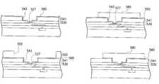
- FIG. 7is a cross-sectional view schematically showing a chip structure according to a sixth embodiment of the present invention.
- FIG. 8is a cross-sectional view schematically showing a chip structure according to a seventh embodiment of the present invention.
- the conductive pads 727 aare exposed to the outside and the conductive pads 727 b are directly electrically connected with the second metal layer 746 .
- the chip structure 700can be electrically connected with external circuits by bonding wires (not shown) onto the conductive pads 727 a .
- the first transition interconnections 722 bthe conductive pads 727 a are electrically connected with the electrostatic discharge circuits 716 and the transition devices 718 respectively.
- the transition devices 718are electrically connected with the electric devices 714 .
- bumpsalso can be formed on the conductive pads 727 a , and the chip structure 700 can be electrically connected with external circuits through the bumps.
- the conductive pads 827 aare exposed to the outside and the conductive pads 827 b are directly electrically connected with the second interconnection scheme 842 .
- Linking traces 829connect the conductive pads 827 a with the conductive pads 827 b .
- the chip structure 800can be electrically connected with external circuits by bonding wires (not shown) onto the conductive pads 827 a .
- the linking traces 829 and conductive pads 827 bthe conductive pads 827 a are electrically connected with the second interconnection scheme 842 .
- the first interconnection scheme 822the second interconnection scheme 842 is electrically connected with the electric devices 814 .
- bumpsalso can be formed on the conductive pads 827 a , and the chip structure 800 can be electrically connected with external circuits through the bumps.
- the shorter the length S of the linking traces 829the better the electrical efficiency of the chip structure 800 . Otherwise, it is possible that the resistance-capacitance delay and the voltage drop will occur and the chip efficiency will be reduced. It is preferred that the length S of the linking traces 829 is less than 5,000 microns.
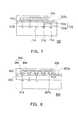
- FIGS. 9-15are various cross-sectional views schematically showing a process of fabricating a chip structure according to an embodiment of the present invention.
- a wafer 502is provided with a substrate 510 , a first built-up layer 520 and a passivation layer 530 .
- the first built-up layer 520is formed on the substrate 510 .
- the first built-up layer 520includes a first interconnection scheme 522 and a first dielectric body 524 , wherein the first interconnection scheme 522 interlaces inside the first dielectric body 524 and is electrically connected to the electric devices 514 .
- the first dielectric body 524is constructed from the lamination of first dielectric multi-layers 521 .
- the first interconnection scheme 522includes first metal multi-layers 526 and plugs 528 . Through the plugs 528 , the first metal layers 526 can be electrically connected with the electric devices 514 or the first metal layers 526 neighbored.
- the first interconnection scheme 522further includes one or more conductive pads 527 (only shows one of them) that are exposed outside the first dielectric body 524 .
- the passivation layer 530is formed on the first built-up layer 520 and is provided with one or more openings 532 exposing the conductive pads 527 . The largest width of the openings 532 ranges from 0.5 to 200 microns for example.
- the openings 532can be formed relatively small, for example, the largest width of the openings 532 ranging from 0.5 to 20 microns, and, correspondingly, the conductive pads 527 can be formed relatively small, the routing density of the top metal layer having the conductive pads 527 can be enhanced. Moreover, due to the design of the openings 532 with relatively small dimensions and high density, correspondingly, the circuits, connecting with the conductive pads 527 , of the second interconnection scheme can be formed small. As a result, the parasitic capacitance generated by the second interconnection scheme can become relatively small.
- a second dielectric sub-layer 541is formed on the passivation layer 530 by, for example, a spin-coating process, wherein the second dielectric sub-layer 541 is made of, for instance, photosensitive organic material.
- one or more via metal openings 543are formed through the second dielectric sub-layer 541 using, for example, a photolithography process.
- the via metal openings 543expose the conductive pads 527 .
- the width of the openings 532is very small, such as 1 micron
- the width of the via metal openings 543can be designed to be larger than that of the openings 532 .
- the width of the via metal openings 543is 3 microns or larger than 3 microns.
- a conductive layer 560is formed onto the second dielectric sub-layer 541 , onto the side walls of the via metal openings 543 , and onto the passivation layer 530 and the conductive pads 527 exposed by the via metal openings 543 .
- the conductive layer 560is made of, for example, titanium-tungsten, titanium or chromium.
- a photoresist 550is formed onto the conductive layer 560 .
- photoresist openingsare formed where a second metal layer is demanded to be fabricated and pass through the photoresist 550 to expose the conductive layer 560 .
- one or more conductive metals 580are filled into the via metal openings 543 and the photoresist openings 552 as shown in FIG. 12 , and are formed over the conductive layer 560 .
- the conductive metals 580include copper, gold, or nickel.
- the photoresist 550is removed as shown in FIG. 13 .
- the conductive layer 560 exposed to the outsideis removed and only remains the conductive layer 560 disposed under the conductive metals 580 .
- another second dielectric sub-layer 570is formed onto the conductive metals 580 and onto the second dielectric sub-layer 541 located at the lower portion.
- the second dielectric sub-layer 570latest formed at the higher portion, is made of, for example, photosensitive material.
- the second built-up layer 540is completed so far.
- the second built-up layer 540includes a second interconnection scheme 542 and a second dielectric body 544 , wherein the second interconnection scheme 542 interlaces inside the second dielectric body 544 .
- the second interconnection scheme 542includes at least one second metal layer 546 and at least one via metal filler 548 .
- the via metal filler 548is constructed from the conductive metals 580 and the conductive layer 560 that are disposed in the via metal opening 543 .
- the second metal layer 546is constructed from the conductive metals 580 and the conductive layer 560 that are outside the via metal opening 543 and on the second dielectric sub-layer 541 .
- the via metal filler 548electrically connects the second metal layers 546 with the conductive pads 527 .
- the cross-sectional area of the opening 532is very small, the cross-sectional area of the via metal opening 543 can be designed to be larger than that of the opening 532 .
- the second dielectric body 544is constructed from the lamination of the second dielectric multi-layers 541 , 570 .
- the thickness L 2 of the second dielectric layers 541 , 570is extremely larger than the thickness L 1 of the first dielectric layers 521 .
- the thickness L 2 of the second dielectric layers 541 , 570ranges from 1 micron to 100 microns.
- the structure, material, and dimension of the second built-up layer 540are detailed in the previous embodiments, and the repeat is omitted herein.
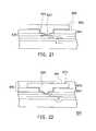
- FIGS. 16-22are various cross-sectional views schematically showing a process of fabricating a chip structure according to another embodiment of the present invention.
- a wafer 602is provided.
- the internal structure of the wafer 602is detailed as the previous embodiments, and the repeat is omitted herein.
- a second dielectric sub-layer 641is formed onto the passivation layer 630 of the wafer 602 by, for example, a spin-coating process, wherein the second dielectric sub-layer 641 is made of, for instance, photosensitive material.
- one or more via metal openings 643are formed through the second dielectric sub-layer 641 by, for example, a photolithography process. The via metal openings 643 expose the conductive pads 627 .
- the width of the via metal openings 643can be designed to be larger than that of the openings 632 . This leads conductive metals, during the following metal-filling process, to be easily filled into the via metal openings 643 and the openings 632 .
- a conductive layer 660is formed onto the second dielectric sub-layer 641 , onto the side walls of the via metal openings 643 , and onto the passivation layer 630 and the conductive pads 627 exposed by the via metal openings 643 .
- the conductive layer 660is made of, for example, titanium-tungsten, titanium or chromium.
- one or more conductive metals 680are formed onto the conductive layer 660 and into the via metal openings 643 , by, for example, an electroplating process or a sputtering process.
- the conductive metals 680include copper, aluminum, gold, or nickel.
- a photoresist 650is formed onto the conductive metals 680 and then by, for example, an exposure process and a lithography process, the photoresist 650 is defined with a line pattern. Only remains the photoresist 650 where a second metal layer is demanded to be formed, and the conductive metals 680 that is not demanded to be formed as the second metal layer is exposed to the outside.
- the conductive metals 680 exposed outside the photoresist 650are removed.
- the conductive layer 660 exposed outside the conductive metals 680are removed by, for example, another etching process.
- the photoresist 650is removed, as shown in FIG. 21 .
- another second dielectric sub-layer 670is formed onto the conductive metals 680 and onto the second dielectric sub-layer 641 located at the lower portion.
- the second dielectric sub-layer 670latest formed at the higher portion, is made of, for example, photosensitive material.
- one or more node openings 672are formed through the second dielectric sub-layer 670 located at the higher portion such that the node openings 672 expose the top conductive metal 680 .
- the exposed conductive metal 680is defined as nodes 647 , through which the chip structure 600 can be electrically connected with external circuits.
- the structure, material, and dimension of the second built-up layer 640are detailed in the previous embodiments, and the repeat is omitted herein.
- the present inventionis not limited to the application of the second metal layer with a signal layer.
- second metal multi-layersalso can be applied in the present invention.
- the fabrication method of the second metal multi-layersis to repeat the above fabrication method of the second metal layer with a single layer.
- the second built-up layer, with second metal multi-layers, fabricated by the above whatever processis finally formed with a second dielectric sub-layer having node openings that expose the second interconnection scheme to be electrically connected with external circuits.
- the whole surface of the second metal layer at the top portioncan be exposed to the outside, and through bumps or conducting wires, the second metal layer can be electrically connected with external circuits.
- the via metal openings of the second dielectric sub-layer at a higher portionexpose the second metal layer at a lower portion so that the conductive metals disposited in the via metal openings electrically connect the upper second metal layer with the lower second metal layer.
- the present inventionhas the following advantages:
- the chip structure of the present inventioncan decline the resistance-capacitance delay, the power of the chip, and the temperature generated by the driving chip since the cross sectional area, the width and the thickness of the traces of the second metal layer are extremely large, since the cross sectional area of the via metal filler is also extremely large, since the second interconnection scheme can be made of low-resistance material, such as copper or gold, since the thickness of the individual second dielectric layer is also extremely large, and since the second dielectric body can be made of organic material, the dielectric constant of which is very low, approximately between 1 ⁇ 3, the practical value depending on the applied organic material.
- each of the power buses or the ground busescan electrically connect with more electric devices than that of prior art. Consequently, the number of the power buses or the ground buses can be reduced and, also, the number of the electrostatic discharge circuits accompanying the power buses or the ground buses can be reduced. In addition, the number of the nodes accompanying the power buses or the ground buses can be reduced.
- the electrostatic discharge circuitscan prevent the electric devices electrically connected with the second interconnection scheme from being damaged by the sudden discharge of high voltage.
- the chip structure of the present inventioncan simplify a design of a substrate board due to the node layout redistribution, fitting the design of the substrate board, of the chip structure by the second interconnection scheme and, besides, the application of the fewer nodes to which ground voltage or power voltage is applied. Moreover, in case the node layout redistribution of various chips by the second interconnection scheme causes the above various chips to be provided with the same node layout, the node layout, matching the same node layout of the above various chips, of the substrate board can be standardized. Therefore, the cost of fabricating the substrate board substantially drops off.
- the second interconnection schemecan be produced using facilities with low accuracy. Therefore, production costs of the chip structure can substantially be reduced.
Landscapes
- Engineering & Computer Science (AREA)
- Power Engineering (AREA)
- Computer Hardware Design (AREA)
- Microelectronics & Electronic Packaging (AREA)
- Physics & Mathematics (AREA)
- Condensed Matter Physics & Semiconductors (AREA)
- General Physics & Mathematics (AREA)
- Manufacturing & Machinery (AREA)
- Geometry (AREA)
- Internal Circuitry In Semiconductor Integrated Circuit Devices (AREA)
- Semiconductor Integrated Circuits (AREA)
- Production Of Multi-Layered Print Wiring Board (AREA)
Abstract
Description
τ=RC=2ερL[L/(Tu.d.Tm)+L/(WS)]
P∝2πfV2kε(tan δ)
where τ is effect of resistance-capacitance delay; P is power loss; ε is dielectric constant of dielectric material; ρ is resistance of traces; L is trace length; W is trace width; S is pitch between traces; Tu.d. is thickness of dielectric material; Tmis trace thickness; tan δ is dielectric loss; V is applied voltage; f is frequency; k is factor of capacitor structure.
Claims (34)
Priority Applications (12)
| Application Number | Priority Date | Filing Date | Title |
|---|---|---|---|
| US10/690,250US6936531B2 (en) | 1998-12-21 | 2003-10-20 | Process of fabricating a chip structure |
| US10/997,145US7470988B2 (en) | 1998-12-21 | 2004-11-24 | Chip structure and process for forming the same |
| US11/123,936US7309920B2 (en) | 1998-12-21 | 2005-05-06 | Chip structure and process for forming the same |
| US11/930,182US7906422B2 (en) | 1998-12-21 | 2007-10-31 | Chip structure and process for forming the same |
| US11/930,181US7932603B2 (en) | 2001-12-13 | 2007-10-31 | Chip structure and process for forming the same |
| US12/025,000US7482259B2 (en) | 2001-12-13 | 2008-02-02 | Chip structure and process for forming the same |
| US12/024,999US7919867B2 (en) | 2001-12-13 | 2008-02-02 | Chip structure and process for forming the same |
| US12/025,001US7915157B2 (en) | 1998-12-21 | 2008-02-02 | Chip structure and process for forming the same |
| US12/024,998US8008776B2 (en) | 2001-12-13 | 2008-02-02 | Chip structure and process for forming the same |
| US12/032,706US7915734B2 (en) | 2001-12-13 | 2008-02-18 | Chip structure and process for forming the same |
| US12/032,707US7906849B2 (en) | 1998-12-21 | 2008-02-18 | Chip structure and process for forming the same |
| US13/191,356US8546947B2 (en) | 2001-12-13 | 2011-07-26 | Chip structure and process for forming the same |
Applications Claiming Priority (12)
| Application Number | Priority Date | Filing Date | Title |
|---|---|---|---|
| US21679198A | 1998-12-21 | 1998-12-21 | |
| US09/251,183US6383916B1 (en) | 1998-12-21 | 1999-02-17 | Top layers of metal for high performance IC's |
| US09/691,497US6495442B1 (en) | 2000-10-18 | 2000-10-18 | Post passivation interconnection schemes on top of the IC chips |
| US09/972,639US6657310B2 (en) | 1998-12-21 | 2001-10-09 | Top layers of metal for high performance IC's |
| TW90130876 | 2001-12-13 | ||
| TW090130876ATW519707B (en) | 2001-12-13 | 2001-12-13 | Chip structure with passivation layer having outer layer connection and its manufacturing process |
| TW90131030ATW511243B (en) | 2001-12-14 | 2001-12-14 | Chip structure and process for making the same |
| TW90131030 | 2001-12-14 | ||
| TW90131796 | 2001-12-21 | ||
| TW90131796ATW519726B (en) | 2001-12-21 | 2001-12-21 | Chip structure and its process |
| US10/124,388US6756295B2 (en) | 1998-12-21 | 2002-04-15 | Chip structure and process for forming the same |
| US10/690,250US6936531B2 (en) | 1998-12-21 | 2003-10-20 | Process of fabricating a chip structure |
Related Parent Applications (2)
| Application Number | Title | Priority Date | Filing Date |
|---|---|---|---|
| US10/124,388DivisionUS6756295B2 (en) | 1998-12-21 | 2002-04-15 | Chip structure and process for forming the same |
| US10/337,673DivisionUS6700162B2 (en) | 1998-12-21 | 2003-01-06 | Chip structure to improve resistance-capacitance delay and reduce energy loss of the chip |
Related Child Applications (2)
| Application Number | Title | Priority Date | Filing Date |
|---|---|---|---|
| US10/997,145DivisionUS7470988B2 (en) | 1998-12-21 | 2004-11-24 | Chip structure and process for forming the same |
| US11/123,936ContinuationUS7309920B2 (en) | 1998-12-21 | 2005-05-06 | Chip structure and process for forming the same |
Publications (2)
| Publication Number | Publication Date |
|---|---|
| US20040079966A1 US20040079966A1 (en) | 2004-04-29 |
| US6936531B2true US6936531B2 (en) | 2005-08-30 |
Family
ID=32111197
Family Applications (6)
| Application Number | Title | Priority Date | Filing Date |
|---|---|---|---|
| US10/690,250Expired - LifetimeUS6936531B2 (en) | 1998-12-21 | 2003-10-20 | Process of fabricating a chip structure |
| US10/997,145Expired - Fee RelatedUS7470988B2 (en) | 1998-12-21 | 2004-11-24 | Chip structure and process for forming the same |
| US11/123,936Expired - Fee RelatedUS7309920B2 (en) | 1998-12-21 | 2005-05-06 | Chip structure and process for forming the same |
| US11/930,182Expired - LifetimeUS7906422B2 (en) | 1998-12-21 | 2007-10-31 | Chip structure and process for forming the same |
| US12/025,001Expired - Fee RelatedUS7915157B2 (en) | 1998-12-21 | 2008-02-02 | Chip structure and process for forming the same |
| US12/032,707Expired - Fee RelatedUS7906849B2 (en) | 1998-12-21 | 2008-02-18 | Chip structure and process for forming the same |
Family Applications After (5)
| Application Number | Title | Priority Date | Filing Date |
|---|---|---|---|
| US10/997,145Expired - Fee RelatedUS7470988B2 (en) | 1998-12-21 | 2004-11-24 | Chip structure and process for forming the same |
| US11/123,936Expired - Fee RelatedUS7309920B2 (en) | 1998-12-21 | 2005-05-06 | Chip structure and process for forming the same |
| US11/930,182Expired - LifetimeUS7906422B2 (en) | 1998-12-21 | 2007-10-31 | Chip structure and process for forming the same |
| US12/025,001Expired - Fee RelatedUS7915157B2 (en) | 1998-12-21 | 2008-02-02 | Chip structure and process for forming the same |
| US12/032,707Expired - Fee RelatedUS7906849B2 (en) | 1998-12-21 | 2008-02-18 | Chip structure and process for forming the same |
Country Status (1)
| Country | Link |
|---|---|
| US (6) | US6936531B2 (en) |
Cited By (3)
| Publication number | Priority date | Publication date | Assignee | Title |
|---|---|---|---|---|
| US20080050912A1 (en)* | 1998-12-21 | 2008-02-28 | Megica Corporation | Chip structure and process for forming the same |
| US20080122099A1 (en)* | 2001-12-13 | 2008-05-29 | Megica Corporation | Chip structure and process for forming the same |
| US7960269B2 (en) | 2005-07-22 | 2011-06-14 | Megica Corporation | Method for forming a double embossing structure |
Families Citing this family (13)
| Publication number | Priority date | Publication date | Assignee | Title |
|---|---|---|---|---|
| US6495442B1 (en) | 2000-10-18 | 2002-12-17 | Magic Corporation | Post passivation interconnection schemes on top of the IC chips |
| US6869870B2 (en)* | 1998-12-21 | 2005-03-22 | Megic Corporation | High performance system-on-chip discrete components using post passivation process |
| JP4449824B2 (en)* | 2005-06-01 | 2010-04-14 | カシオ計算機株式会社 | Semiconductor device and its mounting structure |
| US8344524B2 (en)* | 2006-03-07 | 2013-01-01 | Megica Corporation | Wire bonding method for preventing polymer cracking |
| US7582966B2 (en) | 2006-09-06 | 2009-09-01 | Megica Corporation | Semiconductor chip and method for fabricating the same |
| US8072071B2 (en)* | 2009-02-19 | 2011-12-06 | Infineon Technologies Ag | Semiconductor device including conductive element |
| TW201034150A (en)* | 2009-03-13 | 2010-09-16 | Advanced Semiconductor Eng | Silicon wafer having interconnection metal |
| WO2013089754A1 (en)* | 2011-12-15 | 2013-06-20 | Intel Corporation | Packaged semiconductor die with bumpless die-package interface for bumpless build-up layer (bbul) packages |
| CN103021894B (en)* | 2012-12-30 | 2015-07-08 | 深圳中科系统集成技术有限公司 | Processing method for multi-way electrostatic discharge protection device |
| DK3005298T3 (en)* | 2013-06-06 | 2019-07-22 | Volpara Health Tech Limited | PROCEDURE FOR RECONSTRUCTION OF A PROJECT IMAGE PROJECT |
| KR102798702B1 (en)* | 2019-07-22 | 2025-04-23 | 삼성전자주식회사 | Semiconductor package |
| US20210193519A1 (en)* | 2019-12-19 | 2021-06-24 | Intel Corporation | Inorganic dies with organic interconnect layers and related structures |
| US11817361B2 (en) | 2021-02-12 | 2023-11-14 | Taiwan Semiconductor Manufacturing Co., Ltd. | Passivation structure with planar top surfaces |
Citations (5)
| Publication number | Priority date | Publication date | Assignee | Title |
|---|---|---|---|---|
| US5357403A (en)* | 1990-06-29 | 1994-10-18 | General Electric Company | Adaptive lithography in a high density interconnect structure whose signal layers have fixed patterns |
| US5635767A (en)* | 1995-06-02 | 1997-06-03 | Motorola, Inc. | Semiconductor device having built-in high frequency bypass capacitor |
| US6303423B1 (en)* | 1998-12-21 | 2001-10-16 | Megic Corporation | Method for forming high performance system-on-chip using post passivation process |
| US6756295B2 (en)* | 1998-12-21 | 2004-06-29 | Megic Corporation | Chip structure and process for forming the same |
| US6818540B2 (en)* | 1998-05-18 | 2004-11-16 | Texas Instruments Incorporated | Fine pitch system and method for reinforcing bond pads in semiconductor devices |
Family Cites Families (188)
| Publication number | Priority date | Publication date | Assignee | Title |
|---|---|---|---|---|
| GB1243247A (en) | 1968-03-04 | 1971-08-18 | Texas Instruments Inc | Ohmic contact and electrical interconnection system for electronic devices |
| US3668484A (en)* | 1970-10-28 | 1972-06-06 | Rca Corp | Semiconductor device with multi-level metalization and method of making the same |
| US4303423A (en) | 1978-02-03 | 1981-12-01 | The United States Of America As Represented By The Secretary Of The Army | Engine air cleaner |
| US4189909A (en) | 1978-05-22 | 1980-02-26 | Texas Instruments Incorporated | Integrated injection logic electronic system with voltage regulator for multiplexed liquid crystal display |
| US4300184A (en) | 1979-07-11 | 1981-11-10 | Johnson Controls, Inc. | Conformal coating for electrical circuit assemblies |
| US4423547A (en) | 1981-06-01 | 1984-01-03 | International Business Machines Corporation | Method for forming dense multilevel interconnection metallurgy for semiconductor devices |
| JPS601846A (en) | 1983-06-18 | 1985-01-08 | Toshiba Corp | Multilayer interconnection structure semiconductor device and manufacture thereof |
| US4685998A (en)* | 1984-03-22 | 1987-08-11 | Thomson Components - Mostek Corp. | Process of forming integrated circuits with contact pads in a standard array |
| NL8600021A (en) | 1986-01-08 | 1987-08-03 | Philips Nv | METHOD FOR MANUFACTURING A SEMICONDUCTOR DEVICE APPLYING METALIZATION TO A SEMICONDUCTOR BODY |
| JPH0763064B2 (en)* | 1986-03-31 | 1995-07-05 | 株式会社日立製作所 | Wiring connection method for IC element |
| JPH0789568B2 (en)* | 1986-06-19 | 1995-09-27 | 日本電気株式会社 | Integrated circuit device |
| US5134460A (en)* | 1986-08-11 | 1992-07-28 | International Business Machines Corporation | Aluminum bump, reworkable bump, and titanium nitride structure for tab bonding |
| JPS63283040A (en) | 1987-05-15 | 1988-11-18 | Toshiba Corp | Semiconductor device |
| US5065222A (en) | 1987-11-11 | 1991-11-12 | Seiko Instruments Inc. | Semiconductor device having two-layered passivation film |
| JPH01214141A (en)* | 1988-02-23 | 1989-08-28 | Nec Corp | Flip-chip type semiconductor device |
| JPH0746041Y2 (en) | 1988-02-24 | 1995-10-18 | 三菱電機株式会社 | Vehicular charging power generation system display device |
| US5061985A (en)* | 1988-06-13 | 1991-10-29 | Hitachi, Ltd. | Semiconductor integrated circuit device and process for producing the same |
| US5110762A (en)* | 1988-07-07 | 1992-05-05 | Kabushiki Kaisha Toshiba | Manufacturing a wiring formed inside a semiconductor device |
| US4959705A (en) | 1988-10-17 | 1990-09-25 | Ford Microelectronics, Inc. | Three metal personalization of application specific monolithic microwave integrated circuit |
| US5055907A (en)* | 1989-01-25 | 1991-10-08 | Mosaic, Inc. | Extended integration semiconductor structure with wiring layers |
| US5106461A (en)* | 1989-04-04 | 1992-04-21 | Massachusetts Institute Of Technology | High-density, multi-level interconnects, flex circuits, and tape for tab |
| US5244833A (en)* | 1989-07-26 | 1993-09-14 | International Business Machines Corporation | Method for manufacturing an integrated circuit chip bump electrode using a polymer layer and a photoresist layer |
| US5074947A (en)* | 1989-12-18 | 1991-12-24 | Epoxy Technology, Inc. | Flip chip technology using electrically conductive polymers and dielectrics |
| US5083187A (en) | 1990-05-16 | 1992-01-21 | Texas Instruments Incorporated | Integrated circuit device having bumped power supply buses over active surface areas and method of manufacture thereof |
| US5226232A (en)* | 1990-05-18 | 1993-07-13 | Hewlett-Packard Company | Method for forming a conductive pattern on an integrated circuit |
| FR2666190B1 (en)* | 1990-08-24 | 1996-07-12 | Thomson Csf | METHOD AND DEVICE FOR HERMETIC ENCAPSULATION OF ELECTRONIC COMPONENTS. |
| JP3002512B2 (en)* | 1990-09-10 | 2000-01-24 | 株式会社日立製作所 | Integrated circuit device |
| EP0482247A1 (en) | 1990-10-26 | 1992-04-29 | International Business Machines Corporation | Method for producing an integrated circuit structure with a dense multilayer metallization pattern |
| JP2731040B2 (en) | 1991-02-05 | 1998-03-25 | 三菱電機株式会社 | Method for manufacturing semiconductor device |
| EP0499433B1 (en)* | 1991-02-12 | 1998-04-15 | Matsushita Electronics Corporation | Semiconductor device with improved reliability wiring and method of its fabrication |
| US5476726A (en) | 1992-01-22 | 1995-12-19 | Hitachi, Ltd. | Circuit board with metal layer for solder bonding and electronic circuit device employing the same |
| US5336921A (en) | 1992-01-27 | 1994-08-09 | Motorola, Inc. | Vertical trench inductor |
| US5229221A (en) | 1992-04-16 | 1993-07-20 | Electric Power Research Institute, Inc. | Methods of making anodes for high temperature fuel cells |
| US5384488A (en) | 1992-06-15 | 1995-01-24 | Texas Instruments Incorporated | Configuration and method for positioning semiconductor device bond pads using additional process layers |
| KR940001341A (en)* | 1992-06-29 | 1994-01-11 | 디. 아이. 캐플란 | Instant connection for quick electrical access to electronic devices |
| US5612254A (en)* | 1992-06-29 | 1997-03-18 | Intel Corporation | Methods of forming an interconnect on a semiconductor substrate |
| US6274391B1 (en)* | 1992-10-26 | 2001-08-14 | Texas Instruments Incorporated | HDI land grid array packaged device having electrical and optical interconnects |
| JPH06232379A (en) | 1993-02-01 | 1994-08-19 | Sharp Corp | Solid-state image pickup element |
| US5461333A (en)* | 1993-03-15 | 1995-10-24 | At&T Ipm Corp. | Multi-chip modules having chip-to-chip interconnections with reduced signal voltage level and swing |
| KR950001962A (en) | 1993-06-30 | 1995-01-04 | 김광호 | Semiconductor chip bump |
| KR950004464A (en)* | 1993-07-15 | 1995-02-18 | 김광호 | Manufacturing method of chip bump |
| US5641997A (en)* | 1993-09-14 | 1997-06-24 | Kabushiki Kaisha Toshiba | Plastic-encapsulated semiconductor device |
| US5501006A (en)* | 1993-09-22 | 1996-03-26 | Motorola, Inc. | Method for connection of signals to an integrated circuit |
| US6023103A (en)* | 1994-11-15 | 2000-02-08 | Formfactor, Inc. | Chip-scale carrier for semiconductor devices including mounted spring contacts |
| JP3666893B2 (en) | 1993-11-19 | 2005-06-29 | 株式会社日立製作所 | Semiconductor memory device |
| KR0140646B1 (en)* | 1994-01-12 | 1998-07-15 | 문정환 | Mancefacture of semicouductor device |
| US5508228A (en)* | 1994-02-14 | 1996-04-16 | Microelectronics And Computer Technology Corporation | Compliant electrically connective bumps for an adhesive flip chip integrated circuit device and methods for forming same |
| US5576680A (en) | 1994-03-01 | 1996-11-19 | Amer-Soi | Structure and fabrication process of inductors on semiconductor chip |
| US5434751A (en) | 1994-04-11 | 1995-07-18 | Martin Marietta Corporation | Reworkable high density interconnect structure incorporating a release layer |
| US5652689A (en) | 1994-08-29 | 1997-07-29 | United Microelectronics Corporation | ESD protection circuit located under protected bonding pad |
| US6577148B1 (en) | 1994-08-31 | 2003-06-10 | Motorola, Inc. | Apparatus, method, and wafer used for testing integrated circuits formed on a product wafer |
| JP2658899B2 (en)* | 1994-09-22 | 1997-09-30 | 日本電気株式会社 | Method for manufacturing semiconductor device |
| US5514892A (en) | 1994-09-30 | 1996-05-07 | Motorola, Inc. | Electrostatic discharge protection device |
| US5532512A (en)* | 1994-10-03 | 1996-07-02 | General Electric Company | Direct stacked and flip chip power semiconductor device structures |
| US5892273A (en)* | 1994-10-03 | 1999-04-06 | Kabushiki Kaisha Toshiba | Semiconductor package integral with semiconductor chip |
| US5545909A (en) | 1994-10-19 | 1996-08-13 | Siliconix Incorporated | Electrostatic discharge protection device for integrated circuit |
| US5468984A (en) | 1994-11-02 | 1995-11-21 | Texas Instruments Incorporated | ESD protection structure using LDMOS diodes with thick copper interconnect |
| US5665996A (en)* | 1994-12-30 | 1997-09-09 | Siliconix Incorporated | Vertical power mosfet having thick metal layer to reduce distributed resistance |
| US5665989A (en)* | 1995-01-03 | 1997-09-09 | Lsi Logic | Programmable microsystems in silicon |
| JPH08201432A (en)* | 1995-01-25 | 1996-08-09 | Matsushita Electric Ind Co Ltd | Probe sheet and manufacturing method thereof |
| US5731945A (en)* | 1995-02-22 | 1998-03-24 | International Business Machines Corporation | Multichip semiconductor structures with consolidated circuitry and programmable ESD protection for input/output nodes |
| JPH08235310A (en)* | 1995-02-24 | 1996-09-13 | Nec Corp | Contact character segmenting device |
| WO1996030933A2 (en)* | 1995-03-20 | 1996-10-03 | Mcnc | Solder bump fabrication methods and structure including a titanium barrier layer |
| EP0734059B1 (en) | 1995-03-24 | 2005-11-09 | Shinko Electric Industries Co., Ltd. | Chip sized semiconductor device and a process for making it |
| US5578860A (en) | 1995-05-01 | 1996-11-26 | Motorola, Inc. | Monolithic high frequency integrated circuit structure having a grounded source configuration |
| US5659201A (en)* | 1995-06-05 | 1997-08-19 | Advanced Micro Devices, Inc. | High conductivity interconnection line |
| KR100327442B1 (en) | 1995-07-14 | 2002-06-29 | 구본준, 론 위라하디락사 | Bump Structure and Forming Method of Semiconductor Device |
| US5691248A (en) | 1995-07-26 | 1997-11-25 | International Business Machines Corporation | Methods for precise definition of integrated circuit chip edges |
| US5736792A (en)* | 1995-08-30 | 1998-04-07 | Texas Instruments Incorporated | Method of protecting bond wires during molding and handling |
| US5569956A (en)* | 1995-08-31 | 1996-10-29 | National Semiconductor Corporation | Interposer connecting leadframe and integrated circuit |
| US5539255A (en)* | 1995-09-07 | 1996-07-23 | International Business Machines Corporation | Semiconductor structure having self-aligned interconnection metallization formed from a single layer of metal |
| US5818748A (en)* | 1995-11-21 | 1998-10-06 | International Business Machines Corporation | Chip function separation onto separate stacked chips |
| JP2739853B2 (en)* | 1995-11-28 | 1998-04-15 | 日本電気株式会社 | Semiconductor device manufacturing method and etching method |
| JP2814972B2 (en)* | 1995-12-18 | 1998-10-27 | 日本電気株式会社 | Method for manufacturing semiconductor device |
| US5652182A (en)* | 1995-12-29 | 1997-07-29 | Cypress Semiconductor Corporation | Disposable posts for self-aligned non-enclosed contacts |
| US6111317A (en)* | 1996-01-18 | 2000-08-29 | Kabushiki Kaisha Toshiba | Flip-chip connection type semiconductor integrated circuit device |
| US6022792A (en)* | 1996-03-13 | 2000-02-08 | Seiko Instruments, Inc. | Semiconductor dicing and assembling method |
| US5686764A (en) | 1996-03-20 | 1997-11-11 | Lsi Logic Corporation | Flip chip package with reduced number of package layers |
| US5861740A (en)* | 1996-03-26 | 1999-01-19 | National Research Council Of Canada | Load loss standard for calibrating power loss measurement systems |
| US5792594A (en)* | 1996-04-01 | 1998-08-11 | Motorola, Inc. | Metallization and termination process for an integrated circuit chip |
| KR0176202B1 (en)* | 1996-04-09 | 1999-04-15 | 김광호 | S.O.I transistor and its manufacturing method |
| TW305069B (en)* | 1996-05-06 | 1997-05-11 | United Microelectronics Corp | The IC pad structure and its manufacturing method |
| US5953626A (en)* | 1996-06-05 | 1999-09-14 | Advanced Micro Devices, Inc. | Dissolvable dielectric method |
| US6429120B1 (en)* | 2000-01-18 | 2002-08-06 | Micron Technology, Inc. | Methods and apparatus for making integrated-circuit wiring from copper, silver, gold, and other metals |
| US5883435A (en)* | 1996-07-25 | 1999-03-16 | International Business Machines Corporation | Personalization structure for semiconductor devices |
| US5793272A (en)* | 1996-08-23 | 1998-08-11 | International Business Machines Corporation | Integrated circuit toroidal inductor |
| US5798568A (en) | 1996-08-26 | 1998-08-25 | Motorola, Inc. | Semiconductor component with multi-level interconnect system and method of manufacture |
| JPH10135270A (en)* | 1996-10-31 | 1998-05-22 | Casio Comput Co Ltd | Semiconductor device and manufacturing method thereof |
| US5952726A (en)* | 1996-11-12 | 1999-09-14 | Lsi Logic Corporation | Flip chip bump distribution on die |
| US5818110A (en)* | 1996-11-22 | 1998-10-06 | International Business Machines Corporation | Integrated circuit chip wiring structure with crossover capability and method of manufacturing the same |
| US5969424A (en) | 1997-03-19 | 1999-10-19 | Fujitsu Limited | Semiconductor device with pad structure |
| US5856217A (en)* | 1997-04-10 | 1999-01-05 | Hughes Electronics Corporation | Modulation-doped field-effect transistors and fabrication processes |
| US6143646A (en)* | 1997-06-03 | 2000-11-07 | Motorola Inc. | Dual in-laid integrated circuit structure with selectively positioned low-K dielectric isolation and method of formation |
| US6144100A (en) | 1997-06-05 | 2000-11-07 | Texas Instruments Incorporated | Integrated circuit with bonding layer over active circuitry |
| TW339465B (en) | 1997-06-19 | 1998-09-01 | Ind Tech Res Inst | The method for planarization metal interdielectric layer |
| US6184121B1 (en)* | 1997-07-10 | 2001-02-06 | International Business Machines Corporation | Chip interconnect wiring structure with low dielectric constant insulator and methods for fabricating the same |
| US6100184A (en)* | 1997-08-20 | 2000-08-08 | Sematech, Inc. | Method of making a dual damascene interconnect structure using low dielectric constant material for an inter-level dielectric layer |
| JP3660799B2 (en)* | 1997-09-08 | 2005-06-15 | 株式会社ルネサステクノロジ | Manufacturing method of semiconductor integrated circuit device |
| US5973374A (en) | 1997-09-25 | 1999-10-26 | Integrated Silicon Solution, Inc. | Flash memory array having well contact structures |
| JP3309783B2 (en)* | 1997-10-31 | 2002-07-29 | 日本電気株式会社 | Method for manufacturing semiconductor device |
| US6157079A (en) | 1997-11-10 | 2000-12-05 | Citizen Watch Co., Ltd | Semiconductor device with a bump including a bump electrode film covering a projecting photoresist |
| EP0923126A1 (en) | 1997-12-05 | 1999-06-16 | STMicroelectronics S.r.l. | Integrated electronic device comprising a mechanical stress protection structure |
| US5970376A (en)* | 1997-12-29 | 1999-10-19 | Taiwan Semiconductor Manufacturing Company, Ltd. | Post via etch plasma treatment method for forming with attenuated lateral etching a residue free via through a silsesquioxane spin-on-glass (SOG) dielectric layer |
| US6069078A (en)* | 1997-12-30 | 2000-05-30 | Utmc Microelectronic Systems Inc. | Multi-level interconnect metallization technique |
| TW383482B (en) | 1998-02-13 | 2000-03-01 | United Microelectronics Corp | Multi-layered metal wiring structure for reducing simultaneous switching noise |
| US5959357A (en) | 1998-02-17 | 1999-09-28 | General Electric Company | Fet array for operation at different power levels |
| US6075290A (en)* | 1998-02-26 | 2000-06-13 | National Semiconductor Corporation | Surface mount die: wafer level chip-scale package and process for making the same |
| US6015751A (en)* | 1998-04-06 | 2000-01-18 | Taiwan Semiconductor Manufacturing Company | Self-aligned connection to underlayer metal lines through unlanded via holes |
| JP3955386B2 (en) | 1998-04-09 | 2007-08-08 | 富士通株式会社 | Semiconductor device and manufacturing method thereof |
| US6008102A (en) | 1998-04-09 | 1999-12-28 | Motorola, Inc. | Method of forming a three-dimensional integrated inductor |
| JP3121311B2 (en) | 1998-05-26 | 2000-12-25 | 日本電気株式会社 | Multilayer wiring structure, semiconductor device having the same, and manufacturing method thereof |
| US5943597A (en)* | 1998-06-15 | 1999-08-24 | Motorola, Inc. | Bumped semiconductor device having a trench for stress relief |
| TW367603B (en) | 1998-06-20 | 1999-08-21 | United Microelectronics Corp | Electrostatic discharge protection circuit for SRAM |
| US6245662B1 (en)* | 1998-07-23 | 2001-06-12 | Applied Materials, Inc. | Method of producing an interconnect structure for an integrated circuit |
| US6391771B1 (en) | 1998-07-23 | 2002-05-21 | Applied Materials, Inc. | Integrated circuit interconnect lines having sidewall layers |
| TW374948B (en)* | 1998-07-28 | 1999-11-21 | United Microelectronics Corp | Method of prevention of poisoning trenches in dual damascene process structures and dielectric layer windows |
| US6077726A (en)* | 1998-07-30 | 2000-06-20 | Motorola, Inc. | Method and apparatus for stress relief in solder bump formation on a semiconductor device |
| KR100267108B1 (en) | 1998-09-16 | 2000-10-02 | 윤종용 | Semiconductor device having multi-layer metal interconnection and method fabricating the same |
| US5994766A (en) | 1998-09-21 | 1999-11-30 | Vlsi Technology, Inc. | Flip chip circuit arrangement with redistribution layer that minimizes crosstalk |
| US6071809A (en)* | 1998-09-25 | 2000-06-06 | Rockwell Semiconductor Systems, Inc. | Methods for forming high-performing dual-damascene interconnect structures |
| US6245663B1 (en)* | 1998-09-30 | 2001-06-12 | Conexant Systems, Inc. | IC interconnect structures and methods for making same |
| US6187680B1 (en)* | 1998-10-07 | 2001-02-13 | International Business Machines Corporation | Method/structure for creating aluminum wirebound pad on copper BEOL |
| JP3657788B2 (en)* | 1998-10-14 | 2005-06-08 | 富士通株式会社 | Semiconductor device and manufacturing method thereof |
| JP4095731B2 (en) | 1998-11-09 | 2008-06-04 | 株式会社ルネサステクノロジ | Semiconductor device manufacturing method and semiconductor device |
| US6100590A (en)* | 1998-11-23 | 2000-08-08 | National Semiconductor Corporation | Low capacitance multilevel metal interconnect structure and method of manufacture |
| US6303977B1 (en) | 1998-12-03 | 2001-10-16 | Texas Instruments Incorporated | Fully hermetic semiconductor chip, including sealed edge sides |
| TW445616B (en) | 1998-12-04 | 2001-07-11 | Koninkl Philips Electronics Nv | An integrated circuit device |
| JP2000183104A (en)* | 1998-12-15 | 2000-06-30 | Texas Instr Inc <Ti> | System and method for bonding on an integrated circuit |
| US5998873A (en) | 1998-12-16 | 1999-12-07 | National Semiconductor Corporation | Low contact resistance and low junction leakage metal interconnect contact structure |
| US7381642B2 (en)* | 2004-09-23 | 2008-06-03 | Megica Corporation | Top layers of metal for integrated circuits |
| US6495442B1 (en) | 2000-10-18 | 2002-12-17 | Magic Corporation | Post passivation interconnection schemes on top of the IC chips |
| US7416971B2 (en)* | 2004-09-23 | 2008-08-26 | Megica Corporation | Top layers of metal for integrated circuits |
| US6936531B2 (en)* | 1998-12-21 | 2005-08-30 | Megic Corporation | Process of fabricating a chip structure |
| US6869870B2 (en)* | 1998-12-21 | 2005-03-22 | Megic Corporation | High performance system-on-chip discrete components using post passivation process |
| US7405149B1 (en)* | 1998-12-21 | 2008-07-29 | Megica Corporation | Post passivation method for semiconductor chip or wafer |
| US6383916B1 (en) | 1998-12-21 | 2002-05-07 | M. S. Lin | Top layers of metal for high performance IC's |
| US6359328B1 (en)* | 1998-12-31 | 2002-03-19 | Intel Corporation | Methods for making interconnects and diffusion barriers in integrated circuits |
| JP3530761B2 (en)* | 1999-01-18 | 2004-05-24 | 新光電気工業株式会社 | Semiconductor device |
| JP2000216264A (en)* | 1999-01-22 | 2000-08-04 | Mitsubishi Electric Corp | CMOS logic circuit element, semiconductor device, method of manufacturing the same, and semiconductor circuit design method used in the method of manufacturing the same |
| US6011314A (en)* | 1999-02-01 | 2000-01-04 | Hewlett-Packard Company | Redistribution layer and under bump material structure for converting periphery conductive pads to an array of solder bumps |
| US6191477B1 (en)* | 1999-02-17 | 2001-02-20 | Conexant Systems, Inc. | Leadless chip carrier design and structure |
| US6667552B1 (en) | 1999-02-18 | 2003-12-23 | Advanced Micro Devices, Inc. | Low dielectric metal silicide lined interconnection system |
| US6180426B1 (en)* | 1999-03-01 | 2001-01-30 | Mou-Shiung Lin | High performance sub-system design and assembly |
| TW430935B (en) | 1999-03-19 | 2001-04-21 | Ind Tech Res Inst | Frame type bonding pad structure having a low parasitic capacitance |
| FR2793943B1 (en)* | 1999-05-18 | 2001-07-13 | Memscap | MICRO-COMPONENTS OF THE MICRO-INDUCTANCE OR MICRO-TRANSFORMER TYPE, AND METHOD FOR MANUFACTURING SUCH MICRO-COMPONENTS |
| US6306749B1 (en)* | 1999-06-08 | 2001-10-23 | Winbond Electronics Corp | Bond pad with pad edge strengthening structure |
| US6387734B1 (en)* | 1999-06-11 | 2002-05-14 | Fujikura Ltd. | Semiconductor package, semiconductor device, electronic device and production method for semiconductor package |
| WO2000077844A1 (en)* | 1999-06-15 | 2000-12-21 | Fujikura Ltd. | Semiconductor package, semiconductor device, electronic device, and method of manufacturing semiconductor package |
| TW428298B (en) | 1999-09-17 | 2001-04-01 | United Microelectronics Corp | Manufacturing method and structure for 3D system on chip |
| JP3859403B2 (en)* | 1999-09-22 | 2006-12-20 | 株式会社東芝 | Semiconductor device and manufacturing method thereof |
| US6410435B1 (en)* | 1999-10-01 | 2002-06-25 | Agere Systems Guardian Corp. | Process for fabricating copper interconnect for ULSI integrated circuits |
| US6803302B2 (en) | 1999-11-22 | 2004-10-12 | Freescale Semiconductor, Inc. | Method for forming a semiconductor device having a mechanically robust pad interface |
| US6214630B1 (en) | 1999-12-22 | 2001-04-10 | United Microelectronics Corp. | Wafer level integrated circuit structure and method of manufacturing the same |
| TW441020B (en) | 2000-02-24 | 2001-06-16 | United Microelectronics Corp | Method for forming cap layer of self-aligned copper interconnect |
| EP1139413B1 (en) | 2000-03-24 | 2005-03-16 | Texas Instruments Incorporated | Wire bonding process |
| US6578754B1 (en)* | 2000-04-27 | 2003-06-17 | Advanpack Solutions Pte. Ltd. | Pillar connections for semiconductor chips and method of manufacture |
| US6362087B1 (en)* | 2000-05-05 | 2002-03-26 | Aptos Corporation | Method for fabricating a microelectronic fabrication having formed therein a redistribution structure |
| JP2001339047A (en) | 2000-05-29 | 2001-12-07 | Matsushita Electric Ind Co Ltd | Semiconductor device |
| US6300234B1 (en)* | 2000-06-26 | 2001-10-09 | Motorola, Inc. | Process for forming an electrical device |
| US6683380B2 (en)* | 2000-07-07 | 2004-01-27 | Texas Instruments Incorporated | Integrated circuit with bonding layer over active circuitry |
| JP3440070B2 (en)* | 2000-07-13 | 2003-08-25 | 沖電気工業株式会社 | Wafer and method of manufacturing wafer |
| JP2002198374A (en)* | 2000-10-16 | 2002-07-12 | Sharp Corp | Semiconductor device and method of manufacturing the same |
| TW577152B (en) | 2000-12-18 | 2004-02-21 | Hitachi Ltd | Semiconductor integrated circuit device |
| TW465042B (en) | 2001-01-29 | 2001-11-21 | Macronix Int Co Ltd | Method for forming metal/dielectric multi-level connects |
| US6451685B1 (en)* | 2001-02-05 | 2002-09-17 | Micron Technology, Inc. | Method for multilevel copper interconnects for ultra large scale integration |
| JPWO2002063681A1 (en)* | 2001-02-08 | 2004-06-10 | 株式会社ルネサステクノロジ | Semiconductor integrated circuit device and method of manufacturing the same |
| US20020121702A1 (en)* | 2001-03-01 | 2002-09-05 | Siemens Dematic Electronics Assembly Systems, Inc. | Method and structure of in-situ wafer scale polymer stud grid array contact formation |
| US6653563B2 (en) | 2001-03-30 | 2003-11-25 | Intel Corporation | Alternate bump metallurgy bars for power and ground routing |
| JP3939504B2 (en)* | 2001-04-17 | 2007-07-04 | カシオ計算機株式会社 | Semiconductor device, method for manufacturing the same, and mounting structure |
| US6894399B2 (en)* | 2001-04-30 | 2005-05-17 | Intel Corporation | Microelectronic device having signal distribution functionality on an interfacial layer thereof |
| TW515054B (en)* | 2001-06-13 | 2002-12-21 | Via Tech Inc | Flip chip pad arrangement on chip for reduction of impedance |
| US6593222B2 (en)* | 2001-09-07 | 2003-07-15 | Lattice Corporation | Method to improve the reliability of thermosonic gold to aluminum wire bonds |
| US6515369B1 (en)* | 2001-10-03 | 2003-02-04 | Megic Corporation | High performance system-on-chip using post passivation process |
| US6646347B2 (en) | 2001-11-30 | 2003-11-11 | Motorola, Inc. | Semiconductor power device and method of formation |
| JP4068838B2 (en)* | 2001-12-07 | 2008-03-26 | 株式会社日立製作所 | Manufacturing method of semiconductor device |
| US6798073B2 (en)* | 2001-12-13 | 2004-09-28 | Megic Corporation | Chip structure and process for forming the same |
| US6844631B2 (en)* | 2002-03-13 | 2005-01-18 | Freescale Semiconductor, Inc. | Semiconductor device having a bond pad and method therefor |
| US6614091B1 (en)* | 2002-03-13 | 2003-09-02 | Motorola, Inc. | Semiconductor device having a wire bond pad and method therefor |
| TW531052U (en)* | 2002-04-29 | 2003-05-01 | Via Tech Inc | Flip chip and flip chip packaging substrate |
| US20030218246A1 (en) | 2002-05-22 | 2003-11-27 | Hirofumi Abe | Semiconductor device passing large electric current |
| JP3580803B2 (en)* | 2002-08-09 | 2004-10-27 | 沖電気工業株式会社 | Semiconductor device |
| JP3969295B2 (en)* | 2002-12-02 | 2007-09-05 | セイコーエプソン株式会社 | SEMICONDUCTOR DEVICE, ITS MANUFACTURING METHOD, CIRCUIT BOARD, ELECTRO-OPTICAL DEVICE, AND ELECTRONIC DEVICE |
| US6979647B2 (en) | 2003-09-02 | 2005-12-27 | Texas Instruments Incorporated | Method for chemical etch control of noble metals in the presence of less noble metals |
| US6977435B2 (en) | 2003-09-09 | 2005-12-20 | Intel Corporation | Thick metal layer integrated process flow to improve power delivery and mechanical buffering |
| JP4316351B2 (en) | 2003-10-30 | 2009-08-19 | 株式会社図研 | Printed circuit board design method, printed circuit board design apparatus, program, and computer-readable recording medium |
| JP4221606B2 (en)* | 2005-06-28 | 2009-02-12 | セイコーエプソン株式会社 | Manufacturing method of semiconductor device |
| JP4235834B2 (en)* | 2005-07-12 | 2009-03-11 | セイコーエプソン株式会社 | Manufacturing method of semiconductor device |
| US7582966B2 (en)* | 2006-09-06 | 2009-09-01 | Megica Corporation | Semiconductor chip and method for fabricating the same |
- 2003
- 2003-10-20USUS10/690,250patent/US6936531B2/ennot_activeExpired - Lifetime
- 2004
- 2004-11-24USUS10/997,145patent/US7470988B2/ennot_activeExpired - Fee Related
- 2005
- 2005-05-06USUS11/123,936patent/US7309920B2/ennot_activeExpired - Fee Related
- 2007
- 2007-10-31USUS11/930,182patent/US7906422B2/ennot_activeExpired - Lifetime
- 2008
- 2008-02-02USUS12/025,001patent/US7915157B2/ennot_activeExpired - Fee Related
- 2008-02-18USUS12/032,707patent/US7906849B2/ennot_activeExpired - Fee Related
Patent Citations (5)
| Publication number | Priority date | Publication date | Assignee | Title |
|---|---|---|---|---|
| US5357403A (en)* | 1990-06-29 | 1994-10-18 | General Electric Company | Adaptive lithography in a high density interconnect structure whose signal layers have fixed patterns |
| US5635767A (en)* | 1995-06-02 | 1997-06-03 | Motorola, Inc. | Semiconductor device having built-in high frequency bypass capacitor |
| US6818540B2 (en)* | 1998-05-18 | 2004-11-16 | Texas Instruments Incorporated | Fine pitch system and method for reinforcing bond pads in semiconductor devices |
| US6303423B1 (en)* | 1998-12-21 | 2001-10-16 | Megic Corporation | Method for forming high performance system-on-chip using post passivation process |
| US6756295B2 (en)* | 1998-12-21 | 2004-06-29 | Megic Corporation | Chip structure and process for forming the same |
Cited By (17)
| Publication number | Priority date | Publication date | Assignee | Title |
|---|---|---|---|---|
| US7906422B2 (en) | 1998-12-21 | 2011-03-15 | Megica Corporation | Chip structure and process for forming the same |
| US7915157B2 (en) | 1998-12-21 | 2011-03-29 | Megica Corporation | Chip structure and process for forming the same |
| US20080124918A1 (en)* | 1998-12-21 | 2008-05-29 | Megica Corporation | Chip structure and process for forming the same |
| US7906849B2 (en) | 1998-12-21 | 2011-03-15 | Megica Corporation | Chip structure and process for forming the same |
| US20080050912A1 (en)* | 1998-12-21 | 2008-02-28 | Megica Corporation | Chip structure and process for forming the same |
| US20080142979A1 (en)* | 2001-12-13 | 2008-06-19 | Megica Corporation | Chip structure and process for forming the same |
| US7482259B2 (en)* | 2001-12-13 | 2009-01-27 | Megica Corporation | Chip structure and process for forming the same |
| US20080146019A1 (en)* | 2001-12-13 | 2008-06-19 | Megica Corporation | Chip structure and process for forming the same |
| US20080142978A1 (en)* | 2001-12-13 | 2008-06-19 | Megica Corporation | Chip structure and process for forming the same |
| US7915734B2 (en) | 2001-12-13 | 2011-03-29 | Megica Corporation | Chip structure and process for forming the same |
| US20080122099A1 (en)* | 2001-12-13 | 2008-05-29 | Megica Corporation | Chip structure and process for forming the same |
| US7919867B2 (en) | 2001-12-13 | 2011-04-05 | Megica Corporation | Chip structure and process for forming the same |
| US7932603B2 (en) | 2001-12-13 | 2011-04-26 | Megica Corporation | Chip structure and process for forming the same |
| US8008776B2 (en) | 2001-12-13 | 2011-08-30 | Megica Corporation | Chip structure and process for forming the same |
| US20110278727A1 (en)* | 2001-12-13 | 2011-11-17 | Megica Corporation | Chip structure and process for forming the same |
| US8546947B2 (en)* | 2001-12-13 | 2013-10-01 | Megica Corporation | Chip structure and process for forming the same |
| US7960269B2 (en) | 2005-07-22 | 2011-06-14 | Megica Corporation | Method for forming a double embossing structure |
Also Published As
| Publication number | Publication date |
|---|---|
| US20080124918A1 (en) | 2008-05-29 |
| US20050087844A1 (en) | 2005-04-28 |
| US7915157B2 (en) | 2011-03-29 |
| US7309920B2 (en) | 2007-12-18 |
| US7906849B2 (en) | 2011-03-15 |
| US20050263893A1 (en) | 2005-12-01 |
| US20040079966A1 (en) | 2004-04-29 |
| US7470988B2 (en) | 2008-12-30 |
| US20080136034A1 (en) | 2008-06-12 |
| US7906422B2 (en) | 2011-03-15 |
| US20080050912A1 (en) | 2008-02-28 |
Similar Documents
| Publication | Publication Date | Title |
|---|---|---|
| US6756295B2 (en) | Chip structure and process for forming the same | |
| US7906422B2 (en) | Chip structure and process for forming the same | |
| US6762115B2 (en) | Chip structure and process for forming the same | |
| US8368204B2 (en) | Chip structure and process for forming the same | |
| US8546947B2 (en) | Chip structure and process for forming the same | |
| EP1199750B1 (en) | Post passivation interconnection scheme on top of IC chip | |
| US20050032351A1 (en) | Chip structure and process for forming the same |
Legal Events
| Date | Code | Title | Description |
|---|---|---|---|
| STCF | Information on status: patent grant | Free format text:PATENTED CASE | |
| AS | Assignment | Owner name:MEGICA CORPORATION, TAIWAN Free format text:ASSIGNMENT OF ASSIGNORS INTEREST;ASSIGNOR:MEGIC CORPORATION;REEL/FRAME:017600/0649 Effective date:20060428 | |
| AS | Assignment | Owner name:MEGIC CORPORATION, TAIWAN Free format text:NUNC PRO TUNC ASSIGNMENT;ASSIGNORS:LIN, MOU-SHIUNG;LEE, JIN-YUAN;HUANG, CHING-CHENG;REEL/FRAME:019026/0345 Effective date:20020207 | |
| FEPP | Fee payment procedure | Free format text:PAT HOLDER NO LONGER CLAIMS SMALL ENTITY STATUS, ENTITY STATUS SET TO UNDISCOUNTED (ORIGINAL EVENT CODE: STOL); ENTITY STATUS OF PATENT OWNER: LARGE ENTITY | |
| FPAY | Fee payment | Year of fee payment:4 | |
| FEPP | Fee payment procedure | Free format text:PAYOR NUMBER ASSIGNED (ORIGINAL EVENT CODE: ASPN); ENTITY STATUS OF PATENT OWNER: LARGE ENTITY | |
| FPAY | Fee payment | Year of fee payment:8 | |
| AS | Assignment | Owner name:MEGIT ACQUISITION CORP., CALIFORNIA Free format text:MERGER;ASSIGNOR:MEGICA CORPORATION;REEL/FRAME:031283/0198 Effective date:20130611 | |
| AS | Assignment | Owner name:QUALCOMM INCORPORATED, CALIFORNIA Free format text:ASSIGNMENT OF ASSIGNORS INTEREST;ASSIGNOR:MEGIT ACQUISITION CORP.;REEL/FRAME:033303/0124 Effective date:20140709 | |
| FPAY | Fee payment | Year of fee payment:12 |