US6934785B2 - High speed interface with looped bus - Google Patents
High speed interface with looped busDownload PDFInfo
- Publication number
- US6934785B2 US6934785B2US09/741,821US74182100AUS6934785B2US 6934785 B2US6934785 B2US 6934785B2US 74182100 AUS74182100 AUS 74182100AUS 6934785 B2US6934785 B2US 6934785B2
- Authority
- US
- United States
- Prior art keywords
- data
- bus
- data bus
- segment
- interface circuit
- Prior art date
- Legal status (The legal status is an assumption and is not a legal conclusion. Google has not performed a legal analysis and makes no representation as to the accuracy of the status listed.)
- Expired - Lifetime, expires
Links
Images


Classifications
- G—PHYSICS
- G06—COMPUTING OR CALCULATING; COUNTING
- G06F—ELECTRIC DIGITAL DATA PROCESSING
- G06F13/00—Interconnection of, or transfer of information or other signals between, memories, input/output devices or central processing units
- G06F13/38—Information transfer, e.g. on bus
- G06F13/42—Bus transfer protocol, e.g. handshake; Synchronisation
- G06F13/4265—Bus transfer protocol, e.g. handshake; Synchronisation on a point to point bus
- G—PHYSICS
- G06—COMPUTING OR CALCULATING; COUNTING
- G06F—ELECTRIC DIGITAL DATA PROCESSING
- G06F13/00—Interconnection of, or transfer of information or other signals between, memories, input/output devices or central processing units
- G06F13/14—Handling requests for interconnection or transfer
- G06F13/16—Handling requests for interconnection or transfer for access to memory bus
- G06F13/1668—Details of memory controller
- G06F13/1684—Details of memory controller using multiple buses
- G—PHYSICS
- G06—COMPUTING OR CALCULATING; COUNTING
- G06F—ELECTRIC DIGITAL DATA PROCESSING
- G06F13/00—Interconnection of, or transfer of information or other signals between, memories, input/output devices or central processing units
- G06F13/38—Information transfer, e.g. on bus
- G06F13/40—Bus structure
- G06F13/4063—Device-to-bus coupling
- G06F13/4068—Electrical coupling
- G06F13/4086—Bus impedance matching, e.g. termination
- G—PHYSICS
- G06—COMPUTING OR CALCULATING; COUNTING
- G06F—ELECTRIC DIGITAL DATA PROCESSING
- G06F13/00—Interconnection of, or transfer of information or other signals between, memories, input/output devices or central processing units
- G06F13/38—Information transfer, e.g. on bus
- G06F13/42—Bus transfer protocol, e.g. handshake; Synchronisation
- G06F13/4247—Bus transfer protocol, e.g. handshake; Synchronisation on a daisy chain bus
- Y—GENERAL TAGGING OF NEW TECHNOLOGICAL DEVELOPMENTS; GENERAL TAGGING OF CROSS-SECTIONAL TECHNOLOGIES SPANNING OVER SEVERAL SECTIONS OF THE IPC; TECHNICAL SUBJECTS COVERED BY FORMER USPC CROSS-REFERENCE ART COLLECTIONS [XRACs] AND DIGESTS
- Y02—TECHNOLOGIES OR APPLICATIONS FOR MITIGATION OR ADAPTATION AGAINST CLIMATE CHANGE
- Y02D—CLIMATE CHANGE MITIGATION TECHNOLOGIES IN INFORMATION AND COMMUNICATION TECHNOLOGIES [ICT], I.E. INFORMATION AND COMMUNICATION TECHNOLOGIES AIMING AT THE REDUCTION OF THEIR OWN ENERGY USE
- Y02D10/00—Energy efficient computing, e.g. low power processors, power management or thermal management
Definitions
- the present inventionrelates to improving the performance of a bus for data communications and, more particularly, to a high speed data bus.
- Memory device manufacturersare under continuous pressure to increase the performance and reduce the cost of the memory devices they produce.
- Memory systems for computerstypically provide many memory devices on a common multidrop bus to allow larger storage and transmission capacities than can be obtained with a single memory device.
- data communicated to and from the memory devicesmay be multiplexed for transmission on the bus, thereby reducing the pin count of a memory bus master or controller. For example, a 64-bit wide data word may be transmitted over a 16 bit data bus as four successive 16-bit data word portions.
- such systemstypically include user upgradable or replaceable components to allow future expansion or repair of the memory subsystems.
- these systemsare upgraded on a module basis, where the memory module (e.g., a dual in-line memory module or DIMM) includes several memory devices on a small printed circuit board (PCB), and the module plugs into a connector that provides an electrical connection to the memory subsystem bus.
- the memory modulee.g., a dual in-line memory module or DIMM
- DIMMdual in-line memory module
- PCBsmall printed circuit board
- connection of multiple memory devices to the buscan degrade the performance of the bus since the modules are typically connected in a configuration having electrical stubs which cause signal reflections on the bus. These reflections degrade signal integrity, thus limiting the maximum speed and bandwidth of the system.
- a robust electrical designis required in a high speed multidrop memory bus since the signal integrity must be acceptable throughout the system for lightly loaded systems, that is, where only a small number of module slots are populated, as well as heavily loaded systems where every module slot, or nearly every module slot, is populated.
- the present inventionprovides a method and associated apparatus for improving the performance of a high speed data bus, e.g., a memory bus.
- the inventionsubstantially eliminates bus reflections caused by electrical stubs by connecting system components in a stubless or substantially stubless configuration using a looping bus.
- the inventionprovides a high speed bus having reduced signal reflections.
- the busis looped through data input/output devices, e.g., memory modules, which connect to the bus.
- the inventionprovides a high speed bus between data exchanging devices which maintains a substantially stubless environment.
- a first set of I/O pins and a second set of I/O pinsare provided at data input/output devices, e.g., memory modules, for continuing a looping data bus through each data input/output device connected to the bus.
- An integrated interface circuitis connected to the first set and second set of I/O pins at each device for providing voltage level, encoding type, and data rate conversion for data received from or placed on the bus by the data input/output devices.
- FIG. 1illustrates a bus topology formed in accordance with a first exemplary embodiment of the invention
- FIG. 2illustrates in greater detail a portion of FIG. 1 ;
- FIG. 3illustrates a modified first embodiment of the portion shown in FIG. 2 ;
- FIG. 4illustrates a memory module formed in accordance with a first exemplary embodiment of the invention
- FIG. 5illustrates a bus topology formed in accordance with another exemplary embodiment of the invention
- FIG. 6illustrates a bus topology formed in accordance with another exemplary embodiment of the invention.
- FIG. 7illustrates a timing example in accordance with an exemplary embodiment of the invention
- FIG. 8illustrates a bus topology formed in accordance with another exemplary embodiment of the invention.
- FIG. 9illustrates a portion of the topology of FIG. 1 in accordance with another exemplary embodiment of the invention.
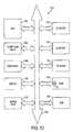
- FIG. 10illustrates a processor system formed in accordance with another exemplary embodiment of the invention.
- FIG. 11illustrates a bus topology formed in accordance with another exemplary embodiment of the invention.
- the inventionprovides a bus system which can be used to interconnect data input/output devices. While the invention is described below with reference to a bus system for a memory system, including memory modules as representative data input/output devices, it should be understood that the bus system of the invention may be used with any type of data input/output device. Likewise, it should be understood that the memory controller described in the context of a memory system may be a bus controller for use with other data input/output devices.
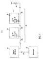
- the processor system 20includes several data input/output devices, which take the form of memory modules 24 , 26 , connected to a memory controller 31 with a looping data bus 28 , and a processor 22 connected to the memory controller 31 via a conventional bus 29 .
- Each of the memory modules 24 , 26has an associated integrated interface circuit 30 connecting each to the looping data bus 28 .
- Each integrated interface circuit 30permits data exchange between the looping data bus 28 and another data pathway, for example, a second data bus 32 , shown at each of the respective memory modules 24 , 26 .
- the second data bus 32is connected to individual memory devices, e.g., DRAM chips, provided on the modules 24 , 26 .
- the looping data bus 28may terminate in a bus terminator, for example a bus terminating resistor 38 .
- memory modules 24 , 26are illustrated, it should be understood that any number of memory modules may be connected to bus 28 in accordance with the invention.
- the looping data bus 28may be a conventional m-bit parallel bus having command and address paths, data paths, and clock (timing) paths.
- the looping data bus 28may have a bus width of any number of parallel data paths, but typically has fewer data paths than a second data bus 32 attached to the interface circuit 30 .
- the looping data bus 28may be 16 bits wide (16 data paths) while the second data bus 32 may be 64 bits wide (64 data paths). Accordingly, and as described below, data from the memory devices connected to the wide bus 32 can be multiplexed by interface circuit 30 onto the narrower bus 28 , while data on bus 28 can be demultiplexed and placed on bus 32 . Accordingly, bus 28 operates at a higher data transfer speed than bus 32 , enabling memory modules 24 , 26 to use lower speed memory devices than would otherwise be required with a high speed bus.
- the integrated interface circuits 30connect to the looping data bus 28 with a low pin count connection.
- the looping data bus 28is continuous through the memory modules 24 , 26 . In this way, memory modules on the looping data bus 28 are connected in a “daisy chain.” This configuration substantially eliminates bus reflections caused by electrical stubs by connecting system components in a substantially stubless configuration which improves the maximum data rate which can be achieved on bus 28 .
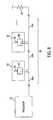
- each integrated interface circuit 30may be connected to the looping data bus 28 by first 42 and second 44 sets of I/O pins (pads).
- a first set of I/O pins 42may be connected to a first bus segment 28 a and a second set of I/O pins 44 may be connected to a second bus segment 28 b .
- the first and second sets of I/O pins 42 , 44are connected internally within the integrated interface circuit 30 and are also connected to a conversion circuit 45 which converts data appearing on the looping data bus 28 for use on a second bus 32 .
- each set of I/O pins 42 and 44will contain 16 pins for the data path, as shown in FIG. 9 .
- Each of the connections between the integrated interface circuit 30 and the buses, such as the looping data bus 28 and the second data bus 32 ,may comprise a respective port 43 , 41 .
- the first port 41includes the first and second sets of I/O pins 42 , 44 .
- Data on the looping data bus 28passes through the first port 41 and is also optionally received by the interface circuit 30 at the first port 41 . Any data received at an interface circuit 30 may then be converted in conversion circuit 45 for use on the second bus 32 .
- Datamay be selectively received by the interface circuit 30 at the first port 41 according to a selection signal received at the integrated interface circuit 30 .
- the selection signalmay be available to the interface circuit 30 on a conventional unlooped memory system command and address bus 135 , as shown in FIG. 2 .
- signals received from a conventional command and address bus 135are captured and decoded by circuitry 133 and may contain instructions for controlling reception of data at integrated interface circuit 30 , for example, a WRITE command directing the integrated interface circuit 30 to receive data available on the looping data bus 28 for storage at a memory device connected to the second data bus 32 .
- the command and address bus 135may also provide each memory module 24 , 26 with address signals for read and write operations.
- selection signalsmay be made available to the interface circuit 30 on a looping command and address bus 235 having a construction similar to the looping data bus 28 for passing selection signals and other information used by the interface circuit 30 .
- the looping command and address bus 235may include segments 235 a , 235 b , 235 c , connecting the integrated interface circuits 30 of the system components, and may be terminated by a bus terminator 238 .
- selection signalssuch as those provided on the command and address bus 135 is to embed selection signals in signals transmitted on the looping data bus 28 shown in FIG. 1 during times when no data is being transmitted.
- the second data bus 32may have operating requirements that differ from those of looping data bus 28 , for example the second data bus 32 may be a higher pin count, higher voltage, lower data rate bus that uses a data encoding different from that of the looping data bus 28 . Therefore, the conversion circuit 45 may convert the data received from the looping data bus 28 for use on the second data bus 32 .
- the conversion circuitmay include a multiplexer/demultiplexer 46 for converting the data rate and number of data paths (e.g., between 16 and 64 data paths), a coder/decoder 47 for appropriately coding/decoding the data between buses 28 and 32 , and a voltage converter 48 , which permit data available on the looping data bus 28 to be appropriately configured for the second bus 32 and vice versa.
- a multiplexer/demultiplexer 46for converting the data rate and number of data paths (e.g., between 16 and 64 data paths)
- a coder/decoder 47for appropriately coding/decoding the data between buses 28 and 32
- a voltage converter 48which permit data available on the looping data bus 28 to be appropriately configured for the second bus 32 and vice versa.
- voltage conversionmay be performed using a voltage converter 48 provided between the looping data bus 28 and the multiplexer/demultiplexer 46 . This is not required, however, and as illustrated in the integrated interface circuit 30 ′ shown in FIG. 3 , voltage conversion may instead be performed at a voltage converter 48 located between the second data bus 32 and the multiplexer/demultiplexer 46 .
- the conversion circuit 45may convert data on the looping data bus 28 for use on the second data bus 32 , but the corresponding conversion in the opposite direction (i.e., from the second data bus 32 to the looping data bus 28 ) is also performed by the conversion circuit 45 in accordance with the invention.
- the integrated interface circuit 30may be turned off when the second data bus 32 is not active, for example in response to selection signals received on the command and address bus 135 .
- the looping function of the first and second sets of I/O pins 42 , 44is passive and the connection between the first and second segments 28 a , 28 b is maintained when an integrated interface circuit 30 is deactivated.
- the integrated interface circuit 30allows devices of different technologies to communicate and exchange data. For example, data may be exchanged between a processor and memory modules 24 , 26 (either directly or through the memory controller 31 ) at high speed using the looping data bus 28 , while the second data bus 32 may connect to memory devices that operate at a lower speed. In this example, the slower data rate of the bus 32 connected to the memory devices allows for the use of inexpensive memory integrated circuits (ICs).
- ICsinexpensive memory integrated circuits
- looping data bus 28may permit the construction of a non-parallel terminated network of devices.
- each of the devices on the busincluding the memory controller 31 and other system devices 24 , 26 , is connected to respective segments 28 a , 28 b , 28 c of the looping data bus 28 to form a “daisy chain.”
- the looping data bus 28is terminated at a bus terminator 38 ; however, in some lower data rate systems, it may be possible to remove the bus terminator since the bus is substantially stubless.
- Such a bus systemmay permit implementation of a memory subsystem with smaller drivers of lower capacitance, lower voltage level due to the lack of a termination resistor in the individual segments 28 a , 28 b (i.e., no DC load current), and having decreased power consumption.
- CMsimple continuity module
- looping bus 28is for a memory system including memory modules 24 , 26 .
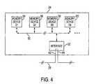
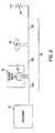
- FIG. 4illustrates one of the memory modules 24 , which includes a plurality of memory devices 54 , 56 , 58 , 60 , mounted on a printed circuit board with the integrated interface circuit 30 .
- Each of the memory devices 54 , 56 , 58 , 60is connected to a memory bus 32 that also connects to the integrated interface circuit 30 .
- the integrated interface circuit 30connects to the looping data bus 28 using the first and second sets of I/O pins 42 , 44 .
- the integrated interface circuit 30receives data from another device connected to the looping data bus 28 , e.g., from a memory controller 31 , converts the data for use on the memory bus 32 , and transmits the data on the memory bus 32 to the individual memory devices 54 , 56 , 58 , 60 .
- the integrated interface circuit 30also receives data available on the memory bus 32 and converts the data for use on the looping data bus 28 . Any necessary data rate, voltage, or other conversions which may be required for data to be exchanged between the looping data bus 28 and the memory bus 32 , for example between the memory controller 31 and the memory devices 54 , 56 , 58 , 60 , are performed at interface 30 . For example, referring to FIGS.
- the integrated interface circuit 30may be connected to the memory controller 31 via the looping data bus 28 , which operates at a 1 Gbit/sec data rate, 1 volt voltage level, and a narrow bus width (low pin count) of 16 data paths (bits).
- the memory bus 32connected to the integrated interface circuit 30 , may operate at a 250 Mbit/sec data rate, 1.8 volt voltage level, and a wide bus width (high pin count) of 64 data paths (bits).
- the WRITE datais transmitted on the looping data bus 28 from the memory controller 31 to the integrated interface circuit 30 , the WRITE data is converted, and transmitted on the memory bus 32 to one or more of the memory devices 54 , 56 , 58 , 60 .
- READ data from the memory devices 54 , 56 , 58 , 60flows in the opposite direction to the memory controller 31 .
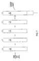
- FIG. 7illustrates a timing example for data exchange between a 16-bit looping data bus 28 and a 64-bit memory bus 32 .
- the received datamay be passed to the memory bus 32 via the 64 data paths of the memory bus 32 .
- This data rate conversion and/or bufferingmay be performed using the multiplexer/demultiplexer 46 (FIG. 2 ). Any other voltage conversions or data encoding/decoding functions needed are performed at the interface circuit 30 as described above and illustrated in FIGS. 2 and 3 .
- the converse data transfer operation from the memory devices 54 , 56 , 58 , 60 , to the memory controller 31is performed. That is, 64 bits of data on bus 32 are multiplexed by interface circuit 30 as four 16 bit data segments which are sequentially placed on looping data bus 28 .
- FIGS. 4-5also illustrate that the memory devices 54 , 56 , 58 , 60 , attached to the memory bus 32 may be mounted on a single memory module 24 ( FIG. 4 ) or, alternatively, may be mounted on respective printed circuit boards (PCBs) or other support structure (FIG. 5 ), but nevertheless each memory device 54 , 56 , 58 , 60 is connected to the memory bus 32 .
- PCBsprinted circuit boards
- the memory controller 31is connected to the looping data bus bus 28 and may exchange data with each of the integrated interface circuits 30 .
- the memory controller 31may be omitted and the processor 22 may be connected to the looping data bus 28 .
- the processor 22may exchange data over the looping data bus 28 with each of the integrated interface circuits 30 , which in turn communicate with memory devices on the memory modules 24 , 26 over the second data buses 32 .
- the embodiment illustrated in FIG. 6advantageously eliminates the need for a separate memory controller chip conventionally used as an intermediary between the processor and the memory devices in a typical computer system.
- the integrated interface circuit 30adds latency to data communications between devices connected to the looping data bus 28 and the second data bus 32 (FIG. 1 )
- any loss in performancemay be alleviated by elimination of a conventional memory controller.
- Some functions formerly provided by a conventional memory controller, such as memory address-to-module mapping,may be performed instead at the processor 22 .
- Other functions formerly performed by a conventional memory controller, such as voltage conversion,may be performed by the integrated interface circuit 30 .
- the latency associated with the memory controllermay be eliminated while still permitting processors and memory devices of differing voltage levels to interoperate.
- Latencycould also be improved by including an additional multiplexer in the integrated interface circuit 30 for performing multiplexing tasks ordinarily performed at individual memory devices on the second data bus 32 . This would allow the multiplexing tasks to be performed at the higher operating rate of the integrated interface circuit 30 .
- FIG. 10illustrates another exemplary processor system which may include a looping data bus 28 .
- the processor systemwhich may be a computer system 100 , for example, generally comprises a central processing unit (CPU) 102 , for example, a microprocessor, that communicates with one or more input/output (I/O) devices 112 , 114 , 116 over a system bus 122 .
- CPUcentral processing unit
- I/Oinput/output
- the computer system 100also includes random access memory (RAM) 118 , a read only memory (ROM) 120 and, in the case of a computer system may include peripheral devices such as a floppy disk drive 104 , a hard drive 106 , a display 108 and a compact disk (CD) ROM drive 110 which also communicate with the processor 102 over the bus 122 .
- the RAM 118includes memory devices communicating with a memory controller 31 via a looping data bus 28 constructed in accordance with the invention. This configuration of the computer system 100 permits high speed communication and/or data transfer between different types of data devices, for example between the processor 102 and the memory controller 31 at the RAM 118 . It should be noted that FIG. 10 is merely representative of another of many different types of processor system architectures which may employ the invention.
- looping data bus 28has been described with reference to a digital data system, e.g., a memory system having memory modules 24 , 26 , the looping data bus 28 can be used to transmit signals of any types, including analog, digital and radio frequency (RF) signals.
- RFradio frequency
Landscapes
- Engineering & Computer Science (AREA)
- Theoretical Computer Science (AREA)
- General Engineering & Computer Science (AREA)
- Physics & Mathematics (AREA)
- General Physics & Mathematics (AREA)
- Computer Hardware Design (AREA)
- Memory System (AREA)
- Bus Control (AREA)
- Dc Digital Transmission (AREA)
Abstract
Description
Claims (57)
Priority Applications (5)
| Application Number | Priority Date | Filing Date | Title |
|---|---|---|---|
| US09/741,821US6934785B2 (en) | 2000-12-22 | 2000-12-22 | High speed interface with looped bus |
| US09/893,616US6871253B2 (en) | 2000-12-22 | 2001-06-29 | Data transmission circuit for memory subsystem, has switching circuit that selectively connects or disconnects two data bus segments to respectively enable data transmission or I/O circuit connection |
| AU2001297792AAU2001297792A1 (en) | 2000-12-22 | 2001-12-11 | High speed interface with looped bus |
| PCT/US2001/051615WO2002084428A2 (en) | 2000-12-22 | 2001-12-11 | High speed interface with looped bus |
| US11/085,270US20050235090A1 (en) | 2000-12-22 | 2005-03-22 | High speed interface with looped bus |
Applications Claiming Priority (1)
| Application Number | Priority Date | Filing Date | Title |
|---|---|---|---|
| US09/741,821US6934785B2 (en) | 2000-12-22 | 2000-12-22 | High speed interface with looped bus |
Related Child Applications (2)
| Application Number | Title | Priority Date | Filing Date |
|---|---|---|---|
| US09/893,616Continuation-In-PartUS6871253B2 (en) | 2000-12-22 | 2001-06-29 | Data transmission circuit for memory subsystem, has switching circuit that selectively connects or disconnects two data bus segments to respectively enable data transmission or I/O circuit connection |
| US11/085,270ContinuationUS20050235090A1 (en) | 2000-12-22 | 2005-03-22 | High speed interface with looped bus |
Publications (2)
| Publication Number | Publication Date |
|---|---|
| US20040225770A1 US20040225770A1 (en) | 2004-11-11 |
| US6934785B2true US6934785B2 (en) | 2005-08-23 |
Family
ID=24982350
Family Applications (3)
| Application Number | Title | Priority Date | Filing Date |
|---|---|---|---|
| US09/741,821Expired - LifetimeUS6934785B2 (en) | 2000-12-22 | 2000-12-22 | High speed interface with looped bus |
| US09/893,616Expired - LifetimeUS6871253B2 (en) | 2000-12-22 | 2001-06-29 | Data transmission circuit for memory subsystem, has switching circuit that selectively connects or disconnects two data bus segments to respectively enable data transmission or I/O circuit connection |
| US11/085,270AbandonedUS20050235090A1 (en) | 2000-12-22 | 2005-03-22 | High speed interface with looped bus |
Family Applications After (2)
| Application Number | Title | Priority Date | Filing Date |
|---|---|---|---|
| US09/893,616Expired - LifetimeUS6871253B2 (en) | 2000-12-22 | 2001-06-29 | Data transmission circuit for memory subsystem, has switching circuit that selectively connects or disconnects two data bus segments to respectively enable data transmission or I/O circuit connection |
| US11/085,270AbandonedUS20050235090A1 (en) | 2000-12-22 | 2005-03-22 | High speed interface with looped bus |
Country Status (3)
| Country | Link |
|---|---|
| US (3) | US6934785B2 (en) |
| AU (1) | AU2001297792A1 (en) |
| WO (1) | WO2002084428A2 (en) |
Cited By (11)
| Publication number | Priority date | Publication date | Assignee | Title |
|---|---|---|---|---|
| US20040107378A1 (en)* | 2002-08-14 | 2004-06-03 | Uwe Guenther | Method and device for the serial transmission of data from a processor module to at least one peripheral element |
| US20050033905A1 (en)* | 2003-08-08 | 2005-02-10 | Leddige Michael W. | Split T-chain memory command and address bus topology |
| US20050055499A1 (en)* | 2003-09-09 | 2005-03-10 | Leddige Michael W. | Circulator chain memory command and address bus topology |
| US20060290438A1 (en)* | 2004-02-27 | 2006-12-28 | Micron Technology, Inc. | Microstrip line dielectric overlay |
| US20070147115A1 (en)* | 2005-12-28 | 2007-06-28 | Fong-Long Lin | Unified memory and controller |
| US20070233933A1 (en)* | 2005-12-28 | 2007-10-04 | Jeremy Wang | Hard disk drive cache memory and playback device |
| US20070245124A1 (en)* | 2003-10-27 | 2007-10-18 | Shinji Furusho | Distributed Memory Type Information Processing System |
| US20080315914A1 (en)* | 2007-05-15 | 2008-12-25 | Samsung Electronics Co., Ltd. | Data transmission device and method thereof |
| US20090070503A1 (en)* | 2000-08-11 | 2009-03-12 | Roy Greeff | Capacitive multidrop bus compensation |
| US20090300260A1 (en)* | 2008-05-28 | 2009-12-03 | Rambus Inc. | Selective switching of a memory bus |
| US20100088442A1 (en)* | 2008-10-06 | 2010-04-08 | Phoenix Contact Gmbh & Co. Kg | Communications entity for communications via a bus-oriented communications network |
Families Citing this family (137)
| Publication number | Priority date | Publication date | Assignee | Title |
|---|---|---|---|---|
| US6597197B1 (en)* | 1999-08-27 | 2003-07-22 | Intel Corporation | I2C repeater with voltage translation |
| US8176296B2 (en) | 2000-10-26 | 2012-05-08 | Cypress Semiconductor Corporation | Programmable microcontroller architecture |
| US8103496B1 (en) | 2000-10-26 | 2012-01-24 | Cypress Semicondutor Corporation | Breakpoint control in an in-circuit emulation system |
| US8160864B1 (en) | 2000-10-26 | 2012-04-17 | Cypress Semiconductor Corporation | In-circuit emulator and pod synchronized boot |
| US8149048B1 (en) | 2000-10-26 | 2012-04-03 | Cypress Semiconductor Corporation | Apparatus and method for programmable power management in a programmable analog circuit block |
| US7765095B1 (en) | 2000-10-26 | 2010-07-27 | Cypress Semiconductor Corporation | Conditional branching in an in-circuit emulation system |
| US6724220B1 (en) | 2000-10-26 | 2004-04-20 | Cyress Semiconductor Corporation | Programmable microcontroller architecture (mixed analog/digital) |
| DE10107100A1 (en)* | 2001-02-13 | 2002-12-05 | Profichip Gmbh | Plug device with integrated diagnosis and evaluation circuit and switchable terminating resistor |
| US7406674B1 (en) | 2001-10-24 | 2008-07-29 | Cypress Semiconductor Corporation | Method and apparatus for generating microcontroller configuration information |
| US8078970B1 (en) | 2001-11-09 | 2011-12-13 | Cypress Semiconductor Corporation | Graphical user interface with user-selectable list-box |
| US8042093B1 (en) | 2001-11-15 | 2011-10-18 | Cypress Semiconductor Corporation | System providing automatic source code generation for personalization and parameterization of user modules |
| US7774190B1 (en) | 2001-11-19 | 2010-08-10 | Cypress Semiconductor Corporation | Sleep and stall in an in-circuit emulation system |
| US7844437B1 (en) | 2001-11-19 | 2010-11-30 | Cypress Semiconductor Corporation | System and method for performing next placements and pruning of disallowed placements for programming an integrated circuit |
| US7770113B1 (en) | 2001-11-19 | 2010-08-03 | Cypress Semiconductor Corporation | System and method for dynamically generating a configuration datasheet |
| US8069405B1 (en) | 2001-11-19 | 2011-11-29 | Cypress Semiconductor Corporation | User interface for efficiently browsing an electronic document using data-driven tabs |
| US6971004B1 (en) | 2001-11-19 | 2005-11-29 | Cypress Semiconductor Corp. | System and method of dynamically reconfiguring a programmable integrated circuit |
| JP2003167839A (en)* | 2001-11-29 | 2003-06-13 | Elpida Memory Inc | Semiconductor memory device |
| DE10162583B4 (en)* | 2001-12-19 | 2004-05-13 | Infineon Technologies Ag | Branched command / address bus architecture for registered storage devices |
| US8103497B1 (en) | 2002-03-28 | 2012-01-24 | Cypress Semiconductor Corporation | External interface for event architecture |
| US7308608B1 (en) | 2002-05-01 | 2007-12-11 | Cypress Semiconductor Corporation | Reconfigurable testing system and method |
| EP1383052B1 (en)* | 2002-07-15 | 2006-03-29 | Infineon Technologies AG | Memory system |
| JP4094370B2 (en)* | 2002-07-31 | 2008-06-04 | エルピーダメモリ株式会社 | Memory module and memory system |
| US7761845B1 (en) | 2002-09-09 | 2010-07-20 | Cypress Semiconductor Corporation | Method for parameterizing a user module |
| US7142461B2 (en)* | 2002-11-20 | 2006-11-28 | Micron Technology, Inc. | Active termination control though on module register |
| KR100464437B1 (en)* | 2002-11-20 | 2004-12-31 | 삼성전자주식회사 | On-Die Termination circuit and method for reducing on-chip DC current and memory system including memory device having the same |
| JP4072424B2 (en)* | 2002-12-02 | 2008-04-09 | エルピーダメモリ株式会社 | Memory system and control method thereof |
| US7096301B2 (en)* | 2003-01-13 | 2006-08-22 | Texas Instruments Incorporated | Communications interface for enabling extension of an internal common bus architecture (CBA) |
| US7308524B2 (en)* | 2003-01-13 | 2007-12-11 | Silicon Pipe, Inc | Memory chain |
| WO2004092904A2 (en)* | 2003-04-10 | 2004-10-28 | Silicon Pipe, Inc. | Memory system having a multiplexed high-speed channel |
| US20040255070A1 (en)* | 2003-06-12 | 2004-12-16 | Larson Thane M. | Inter-integrated circuit router for supporting independent transmission rates |
| US7779212B2 (en) | 2003-10-17 | 2010-08-17 | Micron Technology, Inc. | Method and apparatus for sending data from multiple sources over a communications bus |
| US7085863B2 (en)* | 2003-10-30 | 2006-08-01 | International Business Machines Corporation | I2C device including bus switches and programmable address |
| US7143207B2 (en)* | 2003-11-14 | 2006-11-28 | Intel Corporation | Data accumulation between data path having redrive circuit and memory device |
| US7043591B2 (en)* | 2003-11-19 | 2006-05-09 | Lsi Logic Corporation | Cross switch supporting simultaneous data traffic in opposing directions |
| TWI292533B (en)* | 2003-11-20 | 2008-01-11 | Sunplus Technology Co Ltd | System for accessing a plurality of devices by using single bus and control apparatus therein |
| US7031221B2 (en)* | 2003-12-30 | 2006-04-18 | Intel Corporation | Fixed phase clock and strobe signals in daisy chained chips |
| US7009894B2 (en)* | 2004-02-19 | 2006-03-07 | Intel Corporation | Dynamically activated memory controller data termination |
| US7295049B1 (en) | 2004-03-25 | 2007-11-13 | Cypress Semiconductor Corporation | Method and circuit for rapid alignment of signals |
| US20050228912A1 (en)* | 2004-03-30 | 2005-10-13 | Walker Clinton F | Memory address bus termination control |
| US7389375B2 (en)* | 2004-07-30 | 2008-06-17 | International Business Machines Corporation | System, method and storage medium for a multi-mode memory buffer device |
| US7539800B2 (en) | 2004-07-30 | 2009-05-26 | International Business Machines Corporation | System, method and storage medium for providing segment level sparing |
| US7296129B2 (en) | 2004-07-30 | 2007-11-13 | International Business Machines Corporation | System, method and storage medium for providing a serialized memory interface with a bus repeater |
| US7224595B2 (en) | 2004-07-30 | 2007-05-29 | International Business Machines Corporation | 276-Pin buffered memory module with enhanced fault tolerance |
| US8286125B2 (en) | 2004-08-13 | 2012-10-09 | Cypress Semiconductor Corporation | Model for a hardware device-independent method of defining embedded firmware for programmable systems |
| US8069436B2 (en) | 2004-08-13 | 2011-11-29 | Cypress Semiconductor Corporation | Providing hardware independence to automate code generation of processing device firmware |
| US7501586B2 (en)* | 2004-10-29 | 2009-03-10 | Intel Corporation | Apparatus and method for improving printed circuit board signal layer transitions |
| US7441060B2 (en) | 2004-10-29 | 2008-10-21 | International Business Machines Corporation | System, method and storage medium for providing a service interface to a memory system |
| US7395476B2 (en) | 2004-10-29 | 2008-07-01 | International Business Machines Corporation | System, method and storage medium for providing a high speed test interface to a memory subsystem |
| US7356737B2 (en) | 2004-10-29 | 2008-04-08 | International Business Machines Corporation | System, method and storage medium for testing a memory module |
| US7299313B2 (en) | 2004-10-29 | 2007-11-20 | International Business Machines Corporation | System, method and storage medium for a memory subsystem command interface |
| US7305574B2 (en) | 2004-10-29 | 2007-12-04 | International Business Machines Corporation | System, method and storage medium for bus calibration in a memory subsystem |
| US7512762B2 (en) | 2004-10-29 | 2009-03-31 | International Business Machines Corporation | System, method and storage medium for a memory subsystem with positional read data latency |
| US7331010B2 (en) | 2004-10-29 | 2008-02-12 | International Business Machines Corporation | System, method and storage medium for providing fault detection and correction in a memory subsystem |
| US7277988B2 (en) | 2004-10-29 | 2007-10-02 | International Business Machines Corporation | System, method and storage medium for providing data caching and data compression in a memory subsystem |
| US7332976B1 (en) | 2005-02-04 | 2008-02-19 | Cypress Semiconductor Corporation | Poly-phase frequency synthesis oscillator |
| US7426632B2 (en) | 2005-03-31 | 2008-09-16 | Intel Corporation | Clock distribution for interconnect structures |
| US7990983B2 (en) | 2005-03-31 | 2011-08-02 | Intel Corporation | Modular interconnect structure |
| US9384818B2 (en) | 2005-04-21 | 2016-07-05 | Violin Memory | Memory power management |
| US8112655B2 (en)* | 2005-04-21 | 2012-02-07 | Violin Memory, Inc. | Mesosynchronous data bus apparatus and method of data transmission |
| CN103116565A (en)* | 2005-04-21 | 2013-05-22 | 提琴存储器公司 | Configurable switching element, interconnection network and interconnection method among networks |
| US9582449B2 (en) | 2005-04-21 | 2017-02-28 | Violin Memory, Inc. | Interconnection system |
| US8452929B2 (en)* | 2005-04-21 | 2013-05-28 | Violin Memory Inc. | Method and system for storage of data in non-volatile media |
| US9286198B2 (en) | 2005-04-21 | 2016-03-15 | Violin Memory | Method and system for storage of data in non-volatile media |
| US7400183B1 (en) | 2005-05-05 | 2008-07-15 | Cypress Semiconductor Corporation | Voltage controlled oscillator delay cell and method |
| US8089461B2 (en) | 2005-06-23 | 2012-01-03 | Cypress Semiconductor Corporation | Touch wake for electronic devices |
| US20070057695A1 (en)* | 2005-09-15 | 2007-03-15 | Hermann Ruckerbauer | Semiconductor memory chip with re-drive unit for electrical signals |
| US7555670B2 (en)* | 2005-10-26 | 2009-06-30 | Intel Corporation | Clocking architecture using a bidirectional clock port |
| US7478259B2 (en)* | 2005-10-31 | 2009-01-13 | International Business Machines Corporation | System, method and storage medium for deriving clocks in a memory system |
| US7685392B2 (en)* | 2005-11-28 | 2010-03-23 | International Business Machines Corporation | Providing indeterminate read data latency in a memory system |
| US8085067B1 (en) | 2005-12-21 | 2011-12-27 | Cypress Semiconductor Corporation | Differential-to-single ended signal converter circuit and method |
| CN1996273A (en)* | 2006-01-04 | 2007-07-11 | 鸿富锦精密工业(深圳)有限公司 | High-speed signal transmission circuit |
| US9098641B1 (en)* | 2006-01-30 | 2015-08-04 | Cypress Semiconductor Corporation | Configurable bus |
| KR101239338B1 (en)* | 2006-03-09 | 2013-03-18 | 삼성전자주식회사 | Display device and method of the driving |
| US8067948B2 (en)* | 2006-03-27 | 2011-11-29 | Cypress Semiconductor Corporation | Input/output multiplexer bus |
| US7636813B2 (en) | 2006-05-22 | 2009-12-22 | International Business Machines Corporation | Systems and methods for providing remote pre-fetch buffers |
| US7640386B2 (en)* | 2006-05-24 | 2009-12-29 | International Business Machines Corporation | Systems and methods for providing memory modules with multiple hub devices |
| US7594055B2 (en) | 2006-05-24 | 2009-09-22 | International Business Machines Corporation | Systems and methods for providing distributed technology independent memory controllers |
| US7584336B2 (en) | 2006-06-08 | 2009-09-01 | International Business Machines Corporation | Systems and methods for providing data modification operations in memory subsystems |
| US7610408B2 (en)* | 2006-06-29 | 2009-10-27 | Agilent Technologies, Inc. | Automatic link commissioning |
| US7490186B2 (en)* | 2006-07-26 | 2009-02-10 | International Business Machines Corporation | Memory system having an apportionable data bus and daisy chained memory chips |
| US7546410B2 (en)* | 2006-07-26 | 2009-06-09 | International Business Machines Corporation | Self timed memory chip having an apportionable data bus |
| US7480201B2 (en)* | 2006-07-26 | 2009-01-20 | International Business Machines Corporation | Daisy chainable memory chip |
| US7620763B2 (en)* | 2006-07-26 | 2009-11-17 | International Business Machines Corporation | Memory chip having an apportionable data bus |
| US7660942B2 (en)* | 2006-07-26 | 2010-02-09 | International Business Machines Corporation | Daisy chainable self timed memory chip |
| US7617350B2 (en)* | 2006-07-26 | 2009-11-10 | International Business Machines Corporation | Carrier having daisy chained memory chips |
| US7545664B2 (en)* | 2006-07-26 | 2009-06-09 | International Business Machines Corporation | Memory system having self timed daisy chained memory chips |
| US7673093B2 (en)* | 2006-07-26 | 2010-03-02 | International Business Machines Corporation | Computer system having daisy chained memory chips |
| US7627711B2 (en)* | 2006-07-26 | 2009-12-01 | International Business Machines Corporation | Memory controller for daisy chained memory chips |
| US7660940B2 (en)* | 2006-07-26 | 2010-02-09 | International Business Machines Corporation | Carrier having daisy chain of self timed memory chips |
| US7577811B2 (en)* | 2006-07-26 | 2009-08-18 | International Business Machines Corporation | Memory controller for daisy chained self timed memory chips |
| US7844769B2 (en)* | 2006-07-26 | 2010-11-30 | International Business Machines Corporation | Computer system having an apportionable data bus and daisy chained memory chips |
| KR100782853B1 (en)* | 2006-07-31 | 2007-12-06 | 삼성전자주식회사 | IEEE 1394 network system and its network configuration method |
| US7493439B2 (en)* | 2006-08-01 | 2009-02-17 | International Business Machines Corporation | Systems and methods for providing performance monitoring in a memory system |
| US7669086B2 (en)* | 2006-08-02 | 2010-02-23 | International Business Machines Corporation | Systems and methods for providing collision detection in a memory system |
| US7581073B2 (en) | 2006-08-09 | 2009-08-25 | International Business Machines Corporation | Systems and methods for providing distributed autonomous power management in a memory system |
| US7587559B2 (en)* | 2006-08-10 | 2009-09-08 | International Business Machines Corporation | Systems and methods for memory module power management |
| US7490217B2 (en) | 2006-08-15 | 2009-02-10 | International Business Machines Corporation | Design structure for selecting memory busses according to physical memory organization information stored in virtual address translation tables |
| US7539842B2 (en) | 2006-08-15 | 2009-05-26 | International Business Machines Corporation | Computer memory system for selecting memory buses according to physical memory organization information stored in virtual address translation tables |
| US7477522B2 (en) | 2006-10-23 | 2009-01-13 | International Business Machines Corporation | High density high reliability memory module with a fault tolerant address and command bus |
| US8028186B2 (en) | 2006-10-23 | 2011-09-27 | Violin Memory, Inc. | Skew management in an interconnection system |
| US7870459B2 (en) | 2006-10-23 | 2011-01-11 | International Business Machines Corporation | High density high reliability memory module with power gating and a fault tolerant address and command bus |
| WO2008079911A1 (en) | 2006-12-21 | 2008-07-03 | Rambus Inc. | Dynamic on-die termination of address and command signals |
| US7721140B2 (en) | 2007-01-02 | 2010-05-18 | International Business Machines Corporation | Systems and methods for improving serviceability of a memory system |
| US7606988B2 (en)* | 2007-01-29 | 2009-10-20 | International Business Machines Corporation | Systems and methods for providing a dynamic memory bank page policy |
| US7603526B2 (en)* | 2007-01-29 | 2009-10-13 | International Business Machines Corporation | Systems and methods for providing dynamic memory pre-fetch |
| US8092083B2 (en) | 2007-04-17 | 2012-01-10 | Cypress Semiconductor Corporation | Temperature sensor with digital bandgap |
| US8026739B2 (en) | 2007-04-17 | 2011-09-27 | Cypress Semiconductor Corporation | System level interconnect with programmable switching |
| US8040266B2 (en) | 2007-04-17 | 2011-10-18 | Cypress Semiconductor Corporation | Programmable sigma-delta analog-to-digital converter |
| US9564902B2 (en) | 2007-04-17 | 2017-02-07 | Cypress Semiconductor Corporation | Dynamically configurable and re-configurable data path |
| US7737724B2 (en) | 2007-04-17 | 2010-06-15 | Cypress Semiconductor Corporation | Universal digital block interconnection and channel routing |
| US8130025B2 (en) | 2007-04-17 | 2012-03-06 | Cypress Semiconductor Corporation | Numerical band gap |
| US8516025B2 (en) | 2007-04-17 | 2013-08-20 | Cypress Semiconductor Corporation | Clock driven dynamic datapath chaining |
| US9720805B1 (en) | 2007-04-25 | 2017-08-01 | Cypress Semiconductor Corporation | System and method for controlling a target device |
| US8266575B1 (en) | 2007-04-25 | 2012-09-11 | Cypress Semiconductor Corporation | Systems and methods for dynamically reconfiguring a programmable system on a chip |
| US8065653B1 (en) | 2007-04-25 | 2011-11-22 | Cypress Semiconductor Corporation | Configuration of programmable IC design elements |
| US20090063786A1 (en)* | 2007-08-29 | 2009-03-05 | Hakjune Oh | Daisy-chain memory configuration and usage |
| US8049569B1 (en) | 2007-09-05 | 2011-11-01 | Cypress Semiconductor Corporation | Circuit and method for improving the accuracy of a crystal-less oscillator having dual-frequency modes |
| US8156313B2 (en)* | 2007-09-22 | 2012-04-10 | Navosha Corporation | Chained operation of functional units in integrated circuit by writing DONE/complete value and by reading as GO/start value from same memory location |
| US20090119114A1 (en)* | 2007-11-02 | 2009-05-07 | David Alaniz | Systems and Methods for Enabling Customer Service |
| US8825939B2 (en)* | 2007-12-12 | 2014-09-02 | Conversant Intellectual Property Management Inc. | Semiconductor memory device suitable for interconnection in a ring topology |
| WO2010002397A1 (en)* | 2008-07-01 | 2010-01-07 | Hewlett-Packard Development Company, L.P. | Segmenting bus topology |
| RU2413290C2 (en)* | 2009-04-16 | 2011-02-27 | Николай Иванович Пальченко | Computer architecture with self-contained modules |
| US9448964B2 (en) | 2009-05-04 | 2016-09-20 | Cypress Semiconductor Corporation | Autonomous control in a programmable system |
| KR20120026052A (en)* | 2009-05-15 | 2012-03-16 | 톰슨 라이센싱 | System and method for sharing memory |
| US8164936B2 (en)* | 2009-10-14 | 2012-04-24 | Seagate Technology Llc | Switched memory devices |
| US20110193854A1 (en)* | 2010-02-11 | 2011-08-11 | Apple Inc. | Synchronous bus driving method |
| US8582382B2 (en)* | 2010-03-23 | 2013-11-12 | Mosaid Technologies Incorporated | Memory system having a plurality of serially connected devices |
| US9003096B2 (en)* | 2011-03-16 | 2015-04-07 | Texas Instruments Incorporated | Serial interface |
| CN102339266B (en)* | 2011-10-28 | 2013-08-14 | 中国兵器工业集团第二一四研究所苏州研发中心 | Single data line bidirectional dual voltage communication interface circuit |
| WO2013165995A1 (en) | 2012-04-30 | 2013-11-07 | Thermo King Corporation | Transport refrigeration system controller to engine control unit interface |
| US9190133B2 (en) | 2013-03-11 | 2015-11-17 | Micron Technology, Inc. | Apparatuses and methods for a memory die architecture including an interface memory |
| US9946675B2 (en)* | 2013-03-13 | 2018-04-17 | Atieva, Inc. | Fault-tolerant loop for a communication bus |
| GB201507495D0 (en)* | 2015-04-30 | 2015-06-17 | Cooper Technologies Co | Bus network terminator |
| US10409754B2 (en)* | 2016-04-28 | 2019-09-10 | Smart Modular Technologies, Inc. | Interconnected memory system and method of operation thereof |
| CN112332881B (en)* | 2020-10-19 | 2022-04-26 | 深圳市信锐网科技术有限公司 | Enabling circuit and communication device |
| KR20220112322A (en) | 2021-02-03 | 2022-08-11 | 삼성전자주식회사 | Interface circuit that controlling output impedance of transmitting circuit and image sensor including the same |
| CN116455691A (en)* | 2022-01-06 | 2023-07-18 | 华为技术有限公司 | Communication device and system |
Citations (11)
| Publication number | Priority date | Publication date | Assignee | Title |
|---|---|---|---|---|
| US4974152A (en) | 1986-05-15 | 1990-11-27 | Yves Guiffant | Inserted device for independently connecting auxiliary storage units to a data-processing assembly |
| US5081648A (en) | 1990-03-12 | 1992-01-14 | The Boeing Company | Current mode data bus digital communications system |
| US5452330A (en)* | 1992-07-06 | 1995-09-19 | Digital Equipment Corporation | Bus-oriented switching system for asynchronous transfer mode |
| US5623644A (en) | 1994-08-25 | 1997-04-22 | Intel Corporation | Point-to-point phase-tolerant communication |
| US5631906A (en)* | 1993-03-11 | 1997-05-20 | Liu; Zheng | Medium access control protocol for single bus fair access local area network |
| WO1999019874A1 (en) | 1997-10-10 | 1999-04-22 | Rambus Incorporated | Power control system for synchronous memory device |
| WO1999030240A1 (en) | 1997-12-05 | 1999-06-17 | Intel Corporation | Memory system including a memory module having a memory module controller |
| US6014037A (en)* | 1997-03-27 | 2000-01-11 | Lucent Technologies Inc. | Method and component arrangement for enhancing signal integrity |
| US6233253B1 (en)* | 1997-05-23 | 2001-05-15 | Thomson Licensing S.A. | System for digital data format conversion and bit stream generation |
| US6286067B1 (en)* | 1999-09-21 | 2001-09-04 | Sony Corporation | Method and system for the simplification of leaf-limited bridges |
| US6356984B1 (en)* | 1998-06-30 | 2002-03-12 | Sun Microsystems, Inc. | Digital data processing system having a data bus and a control bus |
Family Cites Families (10)
| Publication number | Priority date | Publication date | Assignee | Title |
|---|---|---|---|---|
| US4470114A (en)* | 1982-03-01 | 1984-09-04 | Burroughs Corporation | High speed interconnection network for a cluster of processors |
| JP3118266B2 (en)* | 1990-03-06 | 2000-12-18 | ゼロックス コーポレイション | Synchronous segment bus and bus communication method |
| IT1274537B (en)* | 1994-05-20 | 1997-07-17 | Fujitsu Ltd | Electronic circuit apparatus for transmitting signals via a bus and semiconductor device for generating a predetermined stable voltage |
| US6182178B1 (en)* | 1998-06-30 | 2001-01-30 | International Business Machines Corporation | Method and system for supporting peripheral component interconnect (PCI) peer-to-peer access across a PCI host bridge supporting multiple PCI buses |
| US6338107B1 (en)* | 1998-12-16 | 2002-01-08 | International Business Machines Corporation | Method and system for providing hot plug of adapter cards in an expanded slot environment |
| AUPQ005099A0 (en)* | 1999-04-29 | 1999-05-20 | Canon Kabushiki Kaisha | Sequential bus architecture |
| US6662260B1 (en)* | 2000-03-28 | 2003-12-09 | Analog Devices, Inc. | Electronic circuits with dynamic bus partitioning |
| US6745268B1 (en)* | 2000-08-11 | 2004-06-01 | Micron Technology, Lnc. | Capacitive multidrop bus compensation |
| US6658509B1 (en)* | 2000-10-03 | 2003-12-02 | Intel Corporation | Multi-tier point-to-point ring memory interface |
| US7010637B2 (en)* | 2002-05-02 | 2006-03-07 | Intel Corporation | Single-ended memory interface system |
- 2000
- 2000-12-22USUS09/741,821patent/US6934785B2/ennot_activeExpired - Lifetime
- 2001
- 2001-06-29USUS09/893,616patent/US6871253B2/ennot_activeExpired - Lifetime
- 2001-12-11WOPCT/US2001/051615patent/WO2002084428A2/ennot_activeApplication Discontinuation
- 2001-12-11AUAU2001297792Apatent/AU2001297792A1/ennot_activeAbandoned
- 2005
- 2005-03-22USUS11/085,270patent/US20050235090A1/ennot_activeAbandoned
Patent Citations (11)
| Publication number | Priority date | Publication date | Assignee | Title |
|---|---|---|---|---|
| US4974152A (en) | 1986-05-15 | 1990-11-27 | Yves Guiffant | Inserted device for independently connecting auxiliary storage units to a data-processing assembly |
| US5081648A (en) | 1990-03-12 | 1992-01-14 | The Boeing Company | Current mode data bus digital communications system |
| US5452330A (en)* | 1992-07-06 | 1995-09-19 | Digital Equipment Corporation | Bus-oriented switching system for asynchronous transfer mode |
| US5631906A (en)* | 1993-03-11 | 1997-05-20 | Liu; Zheng | Medium access control protocol for single bus fair access local area network |
| US5623644A (en) | 1994-08-25 | 1997-04-22 | Intel Corporation | Point-to-point phase-tolerant communication |
| US6014037A (en)* | 1997-03-27 | 2000-01-11 | Lucent Technologies Inc. | Method and component arrangement for enhancing signal integrity |
| US6233253B1 (en)* | 1997-05-23 | 2001-05-15 | Thomson Licensing S.A. | System for digital data format conversion and bit stream generation |
| WO1999019874A1 (en) | 1997-10-10 | 1999-04-22 | Rambus Incorporated | Power control system for synchronous memory device |
| WO1999030240A1 (en) | 1997-12-05 | 1999-06-17 | Intel Corporation | Memory system including a memory module having a memory module controller |
| US6356984B1 (en)* | 1998-06-30 | 2002-03-12 | Sun Microsystems, Inc. | Digital data processing system having a data bus and a control bus |
| US6286067B1 (en)* | 1999-09-21 | 2001-09-04 | Sony Corporation | Method and system for the simplification of leaf-limited bridges |
Non-Patent Citations (5)
| Title |
|---|
| "Hot Rod(TM) High-Speed Serial Link Gallium Arsenide," Gazelle Microcircuits, Inc. pp. 1-35. |
| Alfredo Moncayo et al., "Physical Layer Design of a 1.6 GB/s DRAM Bus", 1999 IEEE. |
| Gustavson, D. "SCI Industrial Takeup and Future Developments," http://www.scizzl.com/Perspectives.html, 13 pages, reviewed Oct. 2, 2000. |
| Gustavson, D., "SCIzzL: The Local Area Memory Port," http://www.scizzl.com, 9 pages, reviewed Oct. 2, 2000. |
| Yasuhiro Konishi et al., "Interface Technologies for Memories and ASICs-Review and Future Direction-", IEICE Transactions on Electronics, vol. E82-C. No. 3 Mar. 1999. |
Cited By (25)
| Publication number | Priority date | Publication date | Assignee | Title |
|---|---|---|---|---|
| US7913005B2 (en)* | 2000-08-11 | 2011-03-22 | Round Rock Research, Llc | Capacitive multidrop bus compensation |
| US20090070503A1 (en)* | 2000-08-11 | 2009-03-12 | Roy Greeff | Capacitive multidrop bus compensation |
| US20040107378A1 (en)* | 2002-08-14 | 2004-06-03 | Uwe Guenther | Method and device for the serial transmission of data from a processor module to at least one peripheral element |
| US7228449B2 (en)* | 2002-08-14 | 2007-06-05 | Robert Bosch Gmbh | Method and device for transmitting a selection signal from a processor to a peripheral by violating a symmetry of transmission of a data signal |
| US20050033905A1 (en)* | 2003-08-08 | 2005-02-10 | Leddige Michael W. | Split T-chain memory command and address bus topology |
| US7194572B2 (en)* | 2003-08-08 | 2007-03-20 | Intel Corporation | Memory system and method to reduce reflection and signal degradation |
| US20050055499A1 (en)* | 2003-09-09 | 2005-03-10 | Leddige Michael W. | Circulator chain memory command and address bus topology |
| US7133962B2 (en)* | 2003-09-09 | 2006-11-07 | Intel Corporation | Circulator chain memory command and address bus topology |
| US7849289B2 (en)* | 2003-10-27 | 2010-12-07 | Turbo Data Laboratories, Inc. | Distributed memory type information processing system |
| US20070245124A1 (en)* | 2003-10-27 | 2007-10-18 | Shinji Furusho | Distributed Memory Type Information Processing System |
| US20060290438A1 (en)* | 2004-02-27 | 2006-12-28 | Micron Technology, Inc. | Microstrip line dielectric overlay |
| US7436267B2 (en) | 2004-02-27 | 2008-10-14 | Micron Technology, Inc. | Microstrip line dielectric overlay |
| US7432774B2 (en) | 2004-02-27 | 2008-10-07 | Micron Technology, Inc. | Microstrip line dielectric overlay |
| US20090025204A1 (en)* | 2004-02-27 | 2009-01-29 | Micron Technology, Inc. | Microstrip line dielectric overlay |
| US9214713B2 (en) | 2004-02-27 | 2015-12-15 | Micron Technology, Inc. | Method of fabricating a microstrip line dielectric overlay |
| US20070233933A1 (en)* | 2005-12-28 | 2007-10-04 | Jeremy Wang | Hard disk drive cache memory and playback device |
| US7519754B2 (en)* | 2005-12-28 | 2009-04-14 | Silicon Storage Technology, Inc. | Hard disk drive cache memory and playback device |
| US20090150588A1 (en)* | 2005-12-28 | 2009-06-11 | Silicon Storage Technology, Inc. | Hard Disk Drive Cache Memory and Playback Device |
| US20070147115A1 (en)* | 2005-12-28 | 2007-06-28 | Fong-Long Lin | Unified memory and controller |
| US20080315914A1 (en)* | 2007-05-15 | 2008-12-25 | Samsung Electronics Co., Ltd. | Data transmission device and method thereof |
| US8135890B2 (en)* | 2008-05-28 | 2012-03-13 | Rambus Inc. | Selective switching of a memory bus |
| US8332556B2 (en) | 2008-05-28 | 2012-12-11 | Rambus Inc. | Selective switching of a memory bus |
| US20090300260A1 (en)* | 2008-05-28 | 2009-12-03 | Rambus Inc. | Selective switching of a memory bus |
| US20100088442A1 (en)* | 2008-10-06 | 2010-04-08 | Phoenix Contact Gmbh & Co. Kg | Communications entity for communications via a bus-oriented communications network |
| US8473656B2 (en)* | 2008-10-06 | 2013-06-25 | Phoenix Contact Gmbh & Co. Kg | Method and system for selecting a communications bus system as a function of an operating mode |
Also Published As
| Publication number | Publication date |
|---|---|
| US20050235090A1 (en) | 2005-10-20 |
| US20040225770A1 (en) | 2004-11-11 |
| US6871253B2 (en) | 2005-03-22 |
| US20020083255A1 (en) | 2002-06-27 |
| WO2002084428A2 (en) | 2002-10-24 |
| AU2001297792A1 (en) | 2002-10-28 |
| WO2002084428A3 (en) | 2003-01-23 |
Similar Documents
| Publication | Publication Date | Title |
|---|---|---|
| US6934785B2 (en) | High speed interface with looped bus | |
| US6882082B2 (en) | Memory repeater | |
| US7526597B2 (en) | Buffered memory having a control bus and dedicated data lines | |
| JP4142950B2 (en) | Apparatus for achieving a buffered daisy chain connection between a memory controller and a memory module | |
| US7051151B2 (en) | Integrated circuit buffer device | |
| US7523248B2 (en) | System having a controller device, a buffer device and a plurality of memory devices | |
| US6625687B1 (en) | Memory module employing a junction circuit for point-to-point connection isolation, voltage translation, data synchronization, and multiplexing/demultiplexing | |
| US7194593B2 (en) | Memory hub with integrated non-volatile memory | |
| US7404032B2 (en) | Configurable width buffered module having switch elements | |
| US7617367B2 (en) | Memory system including a two-on-one link memory subsystem interconnection | |
| US20040230759A1 (en) | Synchronous memory system and also method and protocol for communication in a synchronous memory system |
Legal Events
| Date | Code | Title | Description |
|---|---|---|---|
| AS | Assignment | Owner name:MICRON TECHNOLOGY, INC., IDAHO Free format text:ASSIGNMENT OF ASSIGNORS INTEREST;ASSIGNORS:LEE, TERRY R.;GREEFF, ROY;OVARD, DAVID;REEL/FRAME:016061/0073 Effective date:20010620 | |
| STCF | Information on status: patent grant | Free format text:PATENTED CASE | |
| FEPP | Fee payment procedure | Free format text:PAYER NUMBER DE-ASSIGNED (ORIGINAL EVENT CODE: RMPN); ENTITY STATUS OF PATENT OWNER: LARGE ENTITY Free format text:PAYOR NUMBER ASSIGNED (ORIGINAL EVENT CODE: ASPN); ENTITY STATUS OF PATENT OWNER: LARGE ENTITY | |
| FPAY | Fee payment | Year of fee payment:4 | |
| FPAY | Fee payment | Year of fee payment:8 | |
| AS | Assignment | Owner name:U.S. BANK NATIONAL ASSOCIATION, AS COLLATERAL AGENT, CALIFORNIA Free format text:SECURITY INTEREST;ASSIGNOR:MICRON TECHNOLOGY, INC.;REEL/FRAME:038669/0001 Effective date:20160426 Owner name:U.S. BANK NATIONAL ASSOCIATION, AS COLLATERAL AGEN Free format text:SECURITY INTEREST;ASSIGNOR:MICRON TECHNOLOGY, INC.;REEL/FRAME:038669/0001 Effective date:20160426 | |
| AS | Assignment | Owner name:MORGAN STANLEY SENIOR FUNDING, INC., AS COLLATERAL AGENT, MARYLAND Free format text:PATENT SECURITY AGREEMENT;ASSIGNOR:MICRON TECHNOLOGY, INC.;REEL/FRAME:038954/0001 Effective date:20160426 Owner name:MORGAN STANLEY SENIOR FUNDING, INC., AS COLLATERAL Free format text:PATENT SECURITY AGREEMENT;ASSIGNOR:MICRON TECHNOLOGY, INC.;REEL/FRAME:038954/0001 Effective date:20160426 | |
| FPAY | Fee payment | Year of fee payment:12 | |
| AS | Assignment | Owner name:U.S. BANK NATIONAL ASSOCIATION, AS COLLATERAL AGENT, CALIFORNIA Free format text:CORRECTIVE ASSIGNMENT TO CORRECT THE REPLACE ERRONEOUSLY FILED PATENT #7358718 WITH THE CORRECT PATENT #7358178 PREVIOUSLY RECORDED ON REEL 038669 FRAME 0001. ASSIGNOR(S) HEREBY CONFIRMS THE SECURITY INTEREST;ASSIGNOR:MICRON TECHNOLOGY, INC.;REEL/FRAME:043079/0001 Effective date:20160426 Owner name:U.S. BANK NATIONAL ASSOCIATION, AS COLLATERAL AGEN Free format text:CORRECTIVE ASSIGNMENT TO CORRECT THE REPLACE ERRONEOUSLY FILED PATENT #7358718 WITH THE CORRECT PATENT #7358178 PREVIOUSLY RECORDED ON REEL 038669 FRAME 0001. ASSIGNOR(S) HEREBY CONFIRMS THE SECURITY INTEREST;ASSIGNOR:MICRON TECHNOLOGY, INC.;REEL/FRAME:043079/0001 Effective date:20160426 | |
| AS | Assignment | Owner name:JPMORGAN CHASE BANK, N.A., AS COLLATERAL AGENT, ILLINOIS Free format text:SECURITY INTEREST;ASSIGNORS:MICRON TECHNOLOGY, INC.;MICRON SEMICONDUCTOR PRODUCTS, INC.;REEL/FRAME:047540/0001 Effective date:20180703 Owner name:JPMORGAN CHASE BANK, N.A., AS COLLATERAL AGENT, IL Free format text:SECURITY INTEREST;ASSIGNORS:MICRON TECHNOLOGY, INC.;MICRON SEMICONDUCTOR PRODUCTS, INC.;REEL/FRAME:047540/0001 Effective date:20180703 | |
| AS | Assignment | Owner name:MICRON TECHNOLOGY, INC., IDAHO Free format text:RELEASE BY SECURED PARTY;ASSIGNOR:U.S. BANK NATIONAL ASSOCIATION, AS COLLATERAL AGENT;REEL/FRAME:047243/0001 Effective date:20180629 | |
| AS | Assignment | Owner name:MICRON TECHNOLOGY, INC., IDAHO Free format text:RELEASE BY SECURED PARTY;ASSIGNOR:MORGAN STANLEY SENIOR FUNDING, INC., AS COLLATERAL AGENT;REEL/FRAME:050937/0001 Effective date:20190731 | |
| AS | Assignment | Owner name:MICRON SEMICONDUCTOR PRODUCTS, INC., IDAHO Free format text:RELEASE BY SECURED PARTY;ASSIGNOR:JPMORGAN CHASE BANK, N.A., AS COLLATERAL AGENT;REEL/FRAME:051028/0001 Effective date:20190731 Owner name:MICRON TECHNOLOGY, INC., IDAHO Free format text:RELEASE BY SECURED PARTY;ASSIGNOR:JPMORGAN CHASE BANK, N.A., AS COLLATERAL AGENT;REEL/FRAME:051028/0001 Effective date:20190731 |