US6934674B1 - Clock generation and distribution in an emulation system - Google Patents
Clock generation and distribution in an emulation systemDownload PDFInfo
- Publication number
- US6934674B1 US6934674B1US09/404,923US40492399AUS6934674B1US 6934674 B1US6934674 B1US 6934674B1US 40492399 AUS40492399 AUS 40492399AUS 6934674 B1US6934674 B1US 6934674B1
- Authority
- US
- United States
- Prior art keywords
- clock signal
- derived
- look
- clock
- emulation
- Prior art date
- Legal status (The legal status is an assumption and is not a legal conclusion. Google has not performed a legal analysis and makes no representation as to the accuracy of the status listed.)
- Expired - Lifetime
Links
- 238000000034methodMethods0.000claimsabstractdescription8
- 230000007704transitionEffects0.000claimsdescription6
- 230000000630rising effectEffects0.000description2
- 230000001360synchronised effectEffects0.000description2
- 239000013078crystalSubstances0.000description1
- 238000010586diagramMethods0.000description1
- 230000006870functionEffects0.000description1
- 238000012986modificationMethods0.000description1
- 230000004048modificationEffects0.000description1
- 230000010363phase shiftEffects0.000description1
- 238000012163sequencing techniqueMethods0.000description1
Images


Classifications
- H—ELECTRICITY
- H03—ELECTRONIC CIRCUITRY
- H03K—PULSE TECHNIQUE
- H03K5/00—Manipulating of pulses not covered by one of the other main groups of this subclass
- H03K5/13—Arrangements having a single output and transforming input signals into pulses delivered at desired time intervals
- H03K5/135—Arrangements having a single output and transforming input signals into pulses delivered at desired time intervals by the use of time reference signals, e.g. clock signals
Definitions
- the present inventionrelates to emulation systems, and more particularly, the present invention relates to generation and distribution of multiple synchronized clock signals in an emulation system.
- Prior art clock generation and distribution schemes for emulation systemstypically include a base clock signal, circuitry for frequency multiplying or frequency dividing the base clock signal to generate derived clock signals and circuitry for distributing the derived clock signals.
- the derived clock signalsare typically related to the base clock signal by powers of two.
- the base clock signalmay be frequency divided by two and frequency multiplied by two in order to provide three synchronized clock signals having different frequencies.
- dedicated circuitryis provided to generate each derived clock signal. Additional or different clock signals require additional or different circuitry.
- prior art clock generation and distribution schemesare rigid with respect to the number of derived clock signals provided and the relationship of the derived clock signals to the base clock signal.
- prior art clock generation and distribution schemesare unworkable for emulation systems that employ many clocks.
- the emulation systemWhen providing multiple clock signals derived from a single base clock signal, the emulation system typically starts, stops and resumes the base clock signal to start, stop and resume emulation. However, derived clock signals may not be in phase with the base clock signal. When the derived clock signals are not in phase with the base clock signal and emulation is stopped, emulation stops with respect to a rising or falling edge of the base clock signal. However, in clock domains operating on derived clock signals emulation continues until a subsequent derived clock edge.
- a method and apparatus for generating one or more derived clock signalsis disclosed.
- several derived clock signalsare generated from a look up table.
- a counter circuitcounts base clock cycles and provides an index to the look up table.
- Emulationcan be stopped by stopping the base clock signal, which stops the derived clock signals at a stopping point in the respective derived clock cycles.
- the derived clock signalsdo not continue to a subsequent transition before stopping.
- Emulationis resumed by resuming the base clock signal, which causes the derived clock signals to resume at the stopping point in the respective derived clock signal cycle.
- Derived clock signalscan be resumed where stopped whether at an edge or not to continue emulation thus providing more precise emulation.
- Look up tablesalso increase ease of synchronization between derived clock signals over the prior art because multiple derived clock signals are generated in parallel by similar circuitry that result in approximately the same delay for each derived clock signal and transients or irregularities that occur in the base clock signal are passed to the derived clock signals.
- distribution networksare designed to reduce or eliminate clock skew, the derived clock signals maintain the desired phase relationships.
- FIG. 1is one embodiment of timing generation circuitry for generating derived clock signals according to the present invention.
- FIG. 2is one embodiment of timing generation circuitry for generating derived clock signals having a selection circuit according to the present invention.
- FIG. 3is one embodiment of look up table entries and corresponding derived clock signals according to the present invention.
- FIG. 4is one embodiment of an emulation system in which the present invention may be implemented.
- the present inventionprovides a method and apparatus for generating one or more derived clock signals with a circuit having a look up table.
- a counter circuitcounts base clock cycles and provides an index into the look up table.
- a frequency divider circuitcan be used between the counter circuit and a base clock signal to provide an intermediate clock signal with a frequency that is less than the frequency of the base clock signal.
- the derived clock frequencies and duty cyclesmay be modified by changing the entries in the look up table rather than changing the hardware that provides the derived clock signals as in the prior art thus providing greater flexibility. Additionally, derived clock signals may be resumed where stopped whether at an edge or not to continue emulation thus providing more precise emulation. Look up tables also increase ease of synchronization between derived clock signals over the prior art because multiple derived clock signals are generated in parallel by similar circuitry that result in approximately the same delay for each derived clock signal and transients or irregularities that occur in the base clock signal are passed to the derived clock signal(s).
- a selection circuitis provided to select between the base clock signal and an external clock signal.
- the external clock signalcan be, for example, a derived clock signal from another circuit, an alternative base clock signal, or any other timing signal.
- the selection circuitcan also include a frequency multiplier to multiply the external clock signal.
- FIG. 1is one embodiment of clock generation circuitry according to the present invention.
- Derived clock generation circuit 150receives a base clock signal from base clock generation circuit 100 to generate a derived clock signal.
- Base clock generation circuit 100may be a high frequency oscillator, such as a crystal, or any type of circuit that generates a clock signal with the desired frequency.
- Derived clock generation circuit 150generally comprises frequency divider circuit 152 , counter circuit 154 , and look up table 156 .
- Frequency divider circuit 152receives a clock signal from base clock generation circuit 100 or other source and generates a lower frequency signal as an output.
- Frequency divider circuit 152may be any frequency divider circuit known in the art, or any other type of circuit that provides a frequency division function on the base clock signal received. Alternatively, frequency divider circuit 152 can be replaced by a frequency multiplier circuit to produce a higher frequency clock signal.
- Counter circuit 154receives the output of frequency divider circuit 152 and counts cycles of the clock signal output by frequency divider circuit 152 .
- counter circuit 154may be a 3-bit counter that counts from 0 to 7.
- counter circuit 154may be a different counter circuit, such as a 2-bit, 4-bit, etc. counter, or any other type of counter circuit.
- Look up table 156receives the output of counter circuit 154 , which is used to index entries stored in look up table 156 .
- look up table 156comprises asynchronous memory. Any memory configuration that provides look up table functionality can be used.
- look up table 156has eight entries, each of which store an output signal level. The output of look up table 156 is one or more derived clock signals.
- look up table 156sequentially and cyclically outputs the entries stored therein.
- FIG. 2is one embodiment of clock generation circuitry including selection circuitry according to the present invention.
- the circuitry of FIG. 2is the same as the circuitry of FIG. 1 with the addition of multiplexor 210 and frequency multiplier 220 .
- Multiplexor 210allows for the selection of external clock signals other than the base clock signal to provide input to derived clock generation circuit 150 .
- Select signals (not shown in FIG. 2 ) provided to multiplexor 210can be generated by a central control circuit that provides select signals to multiple multiplexors. Select signals can also be provided by a derived clock generation circuit that is providing an external clock signal to multiplexor 210 . Any manner of generating appropriate control signals known in the art may be used.
- the present inventionprovides greater flexibility for generating derived clock signals then would otherwise be possible.
- frequency multiplier 220is coupled between an external clock signal and multiplexor 210 .
- Frequency multiplier 220multiplies the external clock signal by the appropriate factor to compensate for frequency divider circuit 152 and look up table 156 such that one or more of the derived clock signals has a frequency equal to the external clock signal.
- the circuitry in derived clock generation circuit 150may be shared by the external clock signal and the base clock signal. However, transients in the external clock signal are passed through derived clock generation circuit 150 to the output signal. This provides the proper relationship between the external clock signal and the derived clock signals regardless of inconsistencies and/or transients in the external clock signal or the base clock signal, and the ability to start, stop and resume the derived clock signal at points in addition to clock edges.
- FIG. 3is one embodiment of look up table entries and corresponding derived clock signals according to the present invention.
- FIG. 3includes four examples of look up table entries in an eight-entry table and corresponding derived clock signals. It is important to note, however, that any size of look up table may be used and any number of derived clock signal may be generated according to the present invention.
- the look up table entries of FIG. 3are stored in a single look up table; however, multiple look up tables can be used.
- Look up table entries 300correspond to entries in a look up table, such as look up table 156 (shown in FIG. 1 ).
- the INDEX entryis the index or address corresponding to a signal level entry.
- eight INDEX values labeled 0 through 7are included in a look up table. Of course, any number of INDEX values may be used.
- Look up table entries 300also include CLOCK — 1 entries that indicate signal levels for a derived clock signal for each corresponding INDEX value.
- a logical 0corresponds to a low voltage (e.g., 0 V to 0.7 V) and a logical 1 corresponds to a high voltage (e.g., 3 V to 5V).
- alternative entries and voltage levelsmay also be used.
- the INDEX entriescorrespond to input signals received from counter circuit 154 (shown in FIG. 1 ). As counter circuit 154 counts from 0 to 7 repeatedly, corresponding signal levels are output. Signal 305 corresponds to look up table entries 300 . As the input to the look up table changes, the output from the look up table alternates between a high level and a low level. In this embodiment, the output of the look up table matches the output of the frequency divider circuit in the derived clock generation circuit with the look up table.
- Look up table entries 310generate clock signal 315 with a frequency that is one-half of the frequency of look up table entries 300 .
- An output level (CLOCK — 2)is maintained for two consecutive inputs to the look up table.
- Look up table entries 320generate clock signal 325 with the same frequency as clock signal 315 with a different duty cycle.
- Clock signal 325is low for three counts from the counter circuit and high for one count.
- Look up table entries 330generate clock signal 335 with a frequency that is one-half of the frequency of clock signal 315 .
- Emulationmay be stopped, for example, at time t 3 , which is a rising edge of CLOCK — 1 corresponding to the transition between INDEX values 4 and 5
- t 3does not correspond to an edge for the other clock signals of FIG. 3 .
- emulationtypically continues until the first edge subsequent to t 3 .
- the clock domains corresponding to CLOCK — 2, CLOCK — 3, and CLOCK — 4may not stop at t 3 .
- CLOCK — 2, CLOCK — 3, CLOCK — 4stops between t 3 and t 5 .
- the present inventionallows CLOCK — 2, CLOCK — 3 and CLOCK — 4 to stop and resume at t 3 because look up tables are used to generate clock signals.
- INDEX values input to look up tables 300 , 310 , 320 and 330are sopped at 4. Each clock signal is stopped at that point and does not proceed to the subsequent transition.
- the INDEX valuesare incremented to 5 and proceed according to desired emulation sequencing.
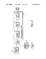
- FIG. 4is one embodiment of an emulation system in which the present invention may be implemented.
- Emulation system 40generally comprises multiple emulation boards interconnected by a bus or other device.
- Emulation system 40also includes a timing generation circuit that provides clock signals to other components of emulation system 40 .
- Emulation system 40includes multiple emulation boards, such as emulation boards 410 and 420 .
- Emulation boardsallow emulation system 40 to emulate hardware designs for testing and debugging purposes.
- each emulation boardincludes multiple programmable devices (not shown in FIG. 4 ), such as field programmable gate array (FPGA) devices.
- Emulation boardsare interconnected by bus 400 .
- bus 400may be replaced by a different device that provides interconnection between multiple boards, such as backplanes and interconnecting boards.
- Timing generation circuit 450is also coupled to bus 400 .
- Timing generation circuit 450provides one or more clock signals to components of emulation system 40 .
- timing generation circuit 450comprises eight circuits for generating derived clock signals. Of course, any number of clock signals may be generated by timing generation circuit 450 .
- timing generation circuit 450includes derived clock generation circuitry, such as the circuitry discussed above with respect to FIGS. 2 and 3 .
- One advantage of generating derived clock signals according to the present inventionis that distributed clock signals do not have a phase shift introduced as a result of using multiple clock generation circuits. Thus, if clock distribution paths are designed to reduce or eliminate skew, the derived clock signals remain in phase, which improves emulation as compared to the prior art.
Landscapes
- Physics & Mathematics (AREA)
- Nonlinear Science (AREA)
- Test And Diagnosis Of Digital Computers (AREA)
- Tests Of Electronic Circuits (AREA)
- Manipulation Of Pulses (AREA)
Abstract
Description
Claims (9)
Priority Applications (7)
| Application Number | Priority Date | Filing Date | Title |
|---|---|---|---|
| US09/404,923US6934674B1 (en) | 1999-09-24 | 1999-09-24 | Clock generation and distribution in an emulation system |
| AT00908546TATE239251T1 (en) | 1999-09-24 | 2000-02-08 | CLOCK GENERATION AND DISTRIBUTION IN AN EMULATION SYSTEM |
| EP00908546AEP1133728B1 (en) | 1999-09-24 | 2000-02-08 | Clock generation and distribution in an emulation system |
| PCT/US2000/003261WO2001024008A1 (en) | 1999-09-24 | 2000-02-08 | Clock generation and distribution in an emulation system |
| DE60002426TDE60002426T2 (en) | 1999-09-24 | 2000-02-08 | CLOCK GENERATION AND DISTRIBUTION IN AN EMULATION SYSTEM |
| AU29867/00AAU2986700A (en) | 1999-09-24 | 2000-02-08 | Clock generation and distribution in an emulation system |
| JP2001500405AJP3537419B2 (en) | 1999-09-24 | 2000-02-08 | Clock generation and distribution in emulation systems |
Applications Claiming Priority (1)
| Application Number | Priority Date | Filing Date | Title |
|---|---|---|---|
| US09/404,923US6934674B1 (en) | 1999-09-24 | 1999-09-24 | Clock generation and distribution in an emulation system |
Publications (1)
| Publication Number | Publication Date |
|---|---|
| US6934674B1true US6934674B1 (en) | 2005-08-23 |
Family
ID=23601588
Family Applications (1)
| Application Number | Title | Priority Date | Filing Date |
|---|---|---|---|
| US09/404,923Expired - LifetimeUS6934674B1 (en) | 1999-09-24 | 1999-09-24 | Clock generation and distribution in an emulation system |
Country Status (7)
| Country | Link |
|---|---|
| US (1) | US6934674B1 (en) |
| EP (1) | EP1133728B1 (en) |
| JP (1) | JP3537419B2 (en) |
| AT (1) | ATE239251T1 (en) |
| AU (1) | AU2986700A (en) |
| DE (1) | DE60002426T2 (en) |
| WO (1) | WO2001024008A1 (en) |
Cited By (42)
| Publication number | Priority date | Publication date | Assignee | Title |
|---|---|---|---|---|
| US7188063B1 (en)* | 2000-10-26 | 2007-03-06 | Cypress Semiconductor Corporation | Capturing test/emulation and enabling real-time debugging using an FPGA for in-circuit emulation |
| US20070283183A1 (en)* | 2005-02-18 | 2007-12-06 | Fujitsu Limited | Apparatus, method and circuit for generating clock, and apparatus, method and program for verifying operation |
| US7737724B2 (en) | 2007-04-17 | 2010-06-15 | Cypress Semiconductor Corporation | Universal digital block interconnection and channel routing |
| US7761845B1 (en) | 2002-09-09 | 2010-07-20 | Cypress Semiconductor Corporation | Method for parameterizing a user module |
| US7765095B1 (en) | 2000-10-26 | 2010-07-27 | Cypress Semiconductor Corporation | Conditional branching in an in-circuit emulation system |
| US7770113B1 (en) | 2001-11-19 | 2010-08-03 | Cypress Semiconductor Corporation | System and method for dynamically generating a configuration datasheet |
| US7774190B1 (en) | 2001-11-19 | 2010-08-10 | Cypress Semiconductor Corporation | Sleep and stall in an in-circuit emulation system |
| CN101847993A (en)* | 2010-04-29 | 2010-09-29 | 北京中星微电子有限公司 | Method and system for configuring clock of audio equipment |
| US7825688B1 (en) | 2000-10-26 | 2010-11-02 | Cypress Semiconductor Corporation | Programmable microcontroller architecture(mixed analog/digital) |
| US7844437B1 (en) | 2001-11-19 | 2010-11-30 | Cypress Semiconductor Corporation | System and method for performing next placements and pruning of disallowed placements for programming an integrated circuit |
| US7893724B2 (en) | 2004-03-25 | 2011-02-22 | Cypress Semiconductor Corporation | Method and circuit for rapid alignment of signals |
| US8026739B2 (en) | 2007-04-17 | 2011-09-27 | Cypress Semiconductor Corporation | System level interconnect with programmable switching |
| US8040266B2 (en) | 2007-04-17 | 2011-10-18 | Cypress Semiconductor Corporation | Programmable sigma-delta analog-to-digital converter |
| US8049569B1 (en) | 2007-09-05 | 2011-11-01 | Cypress Semiconductor Corporation | Circuit and method for improving the accuracy of a crystal-less oscillator having dual-frequency modes |
| US8069405B1 (en) | 2001-11-19 | 2011-11-29 | Cypress Semiconductor Corporation | User interface for efficiently browsing an electronic document using data-driven tabs |
| US8067948B2 (en) | 2006-03-27 | 2011-11-29 | Cypress Semiconductor Corporation | Input/output multiplexer bus |
| US8069428B1 (en) | 2001-10-24 | 2011-11-29 | Cypress Semiconductor Corporation | Techniques for generating microcontroller configuration information |
| US8069436B2 (en) | 2004-08-13 | 2011-11-29 | Cypress Semiconductor Corporation | Providing hardware independence to automate code generation of processing device firmware |
| US8078970B1 (en) | 2001-11-09 | 2011-12-13 | Cypress Semiconductor Corporation | Graphical user interface with user-selectable list-box |
| US8078894B1 (en) | 2007-04-25 | 2011-12-13 | Cypress Semiconductor Corporation | Power management architecture, method and configuration system |
| US8085100B2 (en) | 2005-02-04 | 2011-12-27 | Cypress Semiconductor Corporation | Poly-phase frequency synthesis oscillator |
| US8085067B1 (en) | 2005-12-21 | 2011-12-27 | Cypress Semiconductor Corporation | Differential-to-single ended signal converter circuit and method |
| US8089461B2 (en) | 2005-06-23 | 2012-01-03 | Cypress Semiconductor Corporation | Touch wake for electronic devices |
| US8092083B2 (en) | 2007-04-17 | 2012-01-10 | Cypress Semiconductor Corporation | Temperature sensor with digital bandgap |
| US8103497B1 (en) | 2002-03-28 | 2012-01-24 | Cypress Semiconductor Corporation | External interface for event architecture |
| US8103496B1 (en) | 2000-10-26 | 2012-01-24 | Cypress Semicondutor Corporation | Breakpoint control in an in-circuit emulation system |
| US8120408B1 (en) | 2005-05-05 | 2012-02-21 | Cypress Semiconductor Corporation | Voltage controlled oscillator delay cell and method |
| US8130025B2 (en) | 2007-04-17 | 2012-03-06 | Cypress Semiconductor Corporation | Numerical band gap |
| US8149048B1 (en) | 2000-10-26 | 2012-04-03 | Cypress Semiconductor Corporation | Apparatus and method for programmable power management in a programmable analog circuit block |
| US8160864B1 (en) | 2000-10-26 | 2012-04-17 | Cypress Semiconductor Corporation | In-circuit emulator and pod synchronized boot |
| US8176296B2 (en) | 2000-10-26 | 2012-05-08 | Cypress Semiconductor Corporation | Programmable microcontroller architecture |
| US8229725B1 (en) | 2008-09-29 | 2012-07-24 | Xilinx, Inc. | Method and apparatus for modeling processor-based circuit models |
| US8286125B2 (en) | 2004-08-13 | 2012-10-09 | Cypress Semiconductor Corporation | Model for a hardware device-independent method of defining embedded firmware for programmable systems |
| US8402313B1 (en) | 2002-05-01 | 2013-03-19 | Cypress Semiconductor Corporation | Reconfigurable testing system and method |
| US8499270B1 (en) | 2007-04-25 | 2013-07-30 | Cypress Semiconductor Corporation | Configuration of programmable IC design elements |
| US8516025B2 (en) | 2007-04-17 | 2013-08-20 | Cypress Semiconductor Corporation | Clock driven dynamic datapath chaining |
| US8527949B1 (en) | 2001-11-19 | 2013-09-03 | Cypress Semiconductor Corporation | Graphical user interface for dynamically reconfiguring a programmable device |
| US9448964B2 (en) | 2009-05-04 | 2016-09-20 | Cypress Semiconductor Corporation | Autonomous control in a programmable system |
| US9564902B2 (en) | 2007-04-17 | 2017-02-07 | Cypress Semiconductor Corporation | Dynamically configurable and re-configurable data path |
| US9720805B1 (en) | 2007-04-25 | 2017-08-01 | Cypress Semiconductor Corporation | System and method for controlling a target device |
| US10698662B2 (en) | 2001-11-15 | 2020-06-30 | Cypress Semiconductor Corporation | System providing automatic source code generation for personalization and parameterization of user modules |
| US11194943B2 (en)* | 2017-12-12 | 2021-12-07 | Synopsys, Inc. | FPGA-based hardware emulator system with an inter-FPGA connection switch |
Families Citing this family (2)
| Publication number | Priority date | Publication date | Assignee | Title |
|---|---|---|---|---|
| GB0702597D0 (en) | 2007-02-09 | 2007-03-21 | Texas Instruments Ltd | A debug circuit and a method of debugging |
| DE102008009924B4 (en)* | 2008-02-15 | 2014-10-30 | Jürgen Altenbrunn | Method for generating frequencies |
Citations (36)
| Publication number | Priority date | Publication date | Assignee | Title |
|---|---|---|---|---|
| JPS5072549A (en) | 1973-10-29 | 1975-06-16 | ||
| JPS5668813A (en) | 1979-11-09 | 1981-06-09 | Hitachi Ltd | Timing formation circuit |
| JPS57148231A (en) | 1981-03-10 | 1982-09-13 | Mitsubishi Heavy Ind Ltd | Tester for shock pressurizing |
| JPS57185720A (en) | 1981-05-11 | 1982-11-16 | Akai Electric Co Ltd | Digital pattern generating circuit |
| JPS5814227A (en) | 1981-07-16 | 1983-01-27 | Mitsubishi Electric Corp | timing generation circuit |
| JPS58175035A (en) | 1982-04-06 | 1983-10-14 | Fuji Xerox Co Ltd | Timing generation circuit |
| JPS599765A (en) | 1982-07-08 | 1984-01-19 | Toshiba Corp | Timing control circuit of auxiliary storage device |
| JPS5985527A (en) | 1982-11-08 | 1984-05-17 | Nec Corp | Timing generating circuit |
| JPS6049421A (en) | 1983-08-30 | 1985-03-18 | Fujitsu Ltd | Timing pulse generation method |
| JPS61133830A (en) | 1984-11-30 | 1986-06-21 | ソシエテ・ナシオナル・エルフ・アキテーヌ(プロダクシオン) | Low-temperature high-pressure current body calorimeter |
| JPS61267812A (en) | 1985-05-23 | 1986-11-27 | Matsushita Electric Ind Co Ltd | timing signal generator |
| JPS62194510A (en) | 1986-02-20 | 1987-08-27 | Nec Corp | Output circuit for timing control signal |
| JPS637016A (en) | 1986-06-27 | 1988-01-12 | Fuji Xerox Co Ltd | Clock controller |
| JPS6344215A (en) | 1986-08-08 | 1988-02-25 | Fujitsu Ltd | Clock signal generating device |
| US4759014A (en)* | 1987-05-28 | 1988-07-19 | Ampex Corporation | Asynchronous-to-synchronous digital data multiplexer/demultiplexer with asynchronous clock regeneration |
| JPS63276915A (en) | 1987-02-06 | 1988-11-15 | Nec Corp | Timing signal generating circuit |
| JPS6446118A (en) | 1987-08-13 | 1989-02-20 | Ando Electric | Timing generating circuit |
| JPH01260518A (en) | 1988-04-12 | 1989-10-17 | Nec Corp | Microcomputer |
| JPH02209010A (en) | 1989-02-09 | 1990-08-20 | Mitsubishi Electric Corp | Timing pulse generating circuit |
| JPH0385012A (en) | 1989-08-29 | 1991-04-10 | Canon Inc | Pulse generating circuit |
| US5036473A (en) | 1988-10-05 | 1991-07-30 | Mentor Graphics Corporation | Method of using electronically reconfigurable logic circuits |
| JPH03248213A (en) | 1990-02-27 | 1991-11-06 | Fujitsu Ltd | Timing signal generation circuit |
| JPH04315209A (en) | 1991-04-12 | 1992-11-06 | Mitsubishi Electric Corp | microcomputer |
| JPH06282348A (en) | 1993-03-25 | 1994-10-07 | Shinko Electric Co Ltd | Serial clock generating circuit |
| US5452239A (en) | 1993-01-29 | 1995-09-19 | Quickturn Design Systems, Inc. | Method of removing gated clocks from the clock nets of a netlist for timing sensitive implementation of the netlist in a hardware emulation system |
| JPH07262037A (en) | 1994-03-24 | 1995-10-13 | Hitachi Ltd | Emulator configuration method and emulator expansion board |
| US5491442A (en)* | 1993-07-02 | 1996-02-13 | Tandem Computers Incorporated | Multiple frequency output clock generator system |
| US5623418A (en)* | 1990-04-06 | 1997-04-22 | Lsi Logic Corporation | System and method for creating and validating structural description of electronic system |
| US5701441A (en)* | 1995-08-18 | 1997-12-23 | Xilinx, Inc. | Computer-implemented method of optimizing a design in a time multiplexed programmable logic device |
| US5838956A (en)* | 1996-09-04 | 1998-11-17 | Fujitsu Limited | Clock generating circuit |
| US5954787A (en)* | 1996-12-26 | 1999-09-21 | Daewoo Electronics Co., Ltd. | Method of generating sine/cosine function and apparatus using the same for use in digital signal processor |
| US6055489A (en)* | 1997-04-15 | 2000-04-25 | Intel Corporation | Temperature measurement and compensation scheme |
| US6064247A (en)* | 1998-05-04 | 2000-05-16 | Adaptec, Inc. | Multiple frequency clock generation and synchronization |
| US6135648A (en)* | 1996-11-12 | 2000-10-24 | Lsi Logic Corporation | Hard disk rotational latency simulator |
| US6304125B1 (en)* | 1998-09-04 | 2001-10-16 | Sun Microsystems, Inc. | Method for generating and distribution of polyphase clock signals |
| US6392496B1 (en)* | 1999-06-18 | 2002-05-21 | Lg Information & Communications, Ltd. | Digital PLL circuit having a look-up table and method thereof |
- 1999
- 1999-09-24USUS09/404,923patent/US6934674B1/ennot_activeExpired - Lifetime
- 2000
- 2000-02-08DEDE60002426Tpatent/DE60002426T2/ennot_activeExpired - Lifetime
- 2000-02-08JPJP2001500405Apatent/JP3537419B2/ennot_activeExpired - Lifetime
- 2000-02-08WOPCT/US2000/003261patent/WO2001024008A1/enactiveIP Right Grant
- 2000-02-08ATAT00908546Tpatent/ATE239251T1/ennot_activeIP Right Cessation
- 2000-02-08EPEP00908546Apatent/EP1133728B1/ennot_activeExpired - Lifetime
- 2000-02-08AUAU29867/00Apatent/AU2986700A/ennot_activeAbandoned
Patent Citations (36)
| Publication number | Priority date | Publication date | Assignee | Title |
|---|---|---|---|---|
| JPS5072549A (en) | 1973-10-29 | 1975-06-16 | ||
| JPS5668813A (en) | 1979-11-09 | 1981-06-09 | Hitachi Ltd | Timing formation circuit |
| JPS57148231A (en) | 1981-03-10 | 1982-09-13 | Mitsubishi Heavy Ind Ltd | Tester for shock pressurizing |
| JPS57185720A (en) | 1981-05-11 | 1982-11-16 | Akai Electric Co Ltd | Digital pattern generating circuit |
| JPS5814227A (en) | 1981-07-16 | 1983-01-27 | Mitsubishi Electric Corp | timing generation circuit |
| JPS58175035A (en) | 1982-04-06 | 1983-10-14 | Fuji Xerox Co Ltd | Timing generation circuit |
| JPS599765A (en) | 1982-07-08 | 1984-01-19 | Toshiba Corp | Timing control circuit of auxiliary storage device |
| JPS5985527A (en) | 1982-11-08 | 1984-05-17 | Nec Corp | Timing generating circuit |
| JPS6049421A (en) | 1983-08-30 | 1985-03-18 | Fujitsu Ltd | Timing pulse generation method |
| JPS61133830A (en) | 1984-11-30 | 1986-06-21 | ソシエテ・ナシオナル・エルフ・アキテーヌ(プロダクシオン) | Low-temperature high-pressure current body calorimeter |
| JPS61267812A (en) | 1985-05-23 | 1986-11-27 | Matsushita Electric Ind Co Ltd | timing signal generator |
| JPS62194510A (en) | 1986-02-20 | 1987-08-27 | Nec Corp | Output circuit for timing control signal |
| JPS637016A (en) | 1986-06-27 | 1988-01-12 | Fuji Xerox Co Ltd | Clock controller |
| JPS6344215A (en) | 1986-08-08 | 1988-02-25 | Fujitsu Ltd | Clock signal generating device |
| JPS63276915A (en) | 1987-02-06 | 1988-11-15 | Nec Corp | Timing signal generating circuit |
| US4759014A (en)* | 1987-05-28 | 1988-07-19 | Ampex Corporation | Asynchronous-to-synchronous digital data multiplexer/demultiplexer with asynchronous clock regeneration |
| JPS6446118A (en) | 1987-08-13 | 1989-02-20 | Ando Electric | Timing generating circuit |
| JPH01260518A (en) | 1988-04-12 | 1989-10-17 | Nec Corp | Microcomputer |
| US5036473A (en) | 1988-10-05 | 1991-07-30 | Mentor Graphics Corporation | Method of using electronically reconfigurable logic circuits |
| JPH02209010A (en) | 1989-02-09 | 1990-08-20 | Mitsubishi Electric Corp | Timing pulse generating circuit |
| JPH0385012A (en) | 1989-08-29 | 1991-04-10 | Canon Inc | Pulse generating circuit |
| JPH03248213A (en) | 1990-02-27 | 1991-11-06 | Fujitsu Ltd | Timing signal generation circuit |
| US5623418A (en)* | 1990-04-06 | 1997-04-22 | Lsi Logic Corporation | System and method for creating and validating structural description of electronic system |
| JPH04315209A (en) | 1991-04-12 | 1992-11-06 | Mitsubishi Electric Corp | microcomputer |
| US5452239A (en) | 1993-01-29 | 1995-09-19 | Quickturn Design Systems, Inc. | Method of removing gated clocks from the clock nets of a netlist for timing sensitive implementation of the netlist in a hardware emulation system |
| JPH06282348A (en) | 1993-03-25 | 1994-10-07 | Shinko Electric Co Ltd | Serial clock generating circuit |
| US5491442A (en)* | 1993-07-02 | 1996-02-13 | Tandem Computers Incorporated | Multiple frequency output clock generator system |
| JPH07262037A (en) | 1994-03-24 | 1995-10-13 | Hitachi Ltd | Emulator configuration method and emulator expansion board |
| US5701441A (en)* | 1995-08-18 | 1997-12-23 | Xilinx, Inc. | Computer-implemented method of optimizing a design in a time multiplexed programmable logic device |
| US5838956A (en)* | 1996-09-04 | 1998-11-17 | Fujitsu Limited | Clock generating circuit |
| US6135648A (en)* | 1996-11-12 | 2000-10-24 | Lsi Logic Corporation | Hard disk rotational latency simulator |
| US5954787A (en)* | 1996-12-26 | 1999-09-21 | Daewoo Electronics Co., Ltd. | Method of generating sine/cosine function and apparatus using the same for use in digital signal processor |
| US6055489A (en)* | 1997-04-15 | 2000-04-25 | Intel Corporation | Temperature measurement and compensation scheme |
| US6064247A (en)* | 1998-05-04 | 2000-05-16 | Adaptec, Inc. | Multiple frequency clock generation and synchronization |
| US6304125B1 (en)* | 1998-09-04 | 2001-10-16 | Sun Microsystems, Inc. | Method for generating and distribution of polyphase clock signals |
| US6392496B1 (en)* | 1999-06-18 | 2002-05-21 | Lg Information & Communications, Ltd. | Digital PLL circuit having a look-up table and method thereof |
Non-Patent Citations (7)
| Title |
|---|
| "Translation of an Office Action of Japanese Patent Office," from counterpart Japanese Application No. 2001-500405, 3 pgs., mailed Aug. 27, 2002. |
| "Translation of Final Rejection of the Japanese Patent Office," from counterpart Japanese Application No. 2001-500405, mailed Mar. 25, 2003 (2 pages). |
| International Search Report for PCT/US00/03261, issued Jun. 23, 2000. |
| Mel Bazes, "An Interpolating Clock Synthesizer," IEEE J. of Solid State Circuits, vol. 31, No. 9, pp. 1295-1301 (Sep. 1996). |
| Rahkonen, T.; Eksyma, H., "A 3-V programmable clock generator with a built-in phase interpolator," Proceedings of the 1998 Midwest Symposium on Circuits and Systems, 1998, pp.: 488-491.* |
| Translation of Oct. 28, 2003 Office Action in Japanese application 2001-500405. |
| XILINX, "The Programmable Gate Array Design Handbook," First Edition, 1986, pp. i-A-10. |
Cited By (59)
| Publication number | Priority date | Publication date | Assignee | Title |
|---|---|---|---|---|
| US8736303B2 (en) | 2000-10-26 | 2014-05-27 | Cypress Semiconductor Corporation | PSOC architecture |
| US9766650B2 (en) | 2000-10-26 | 2017-09-19 | Cypress Semiconductor Corporation | Microcontroller programmable system on a chip with programmable interconnect |
| US10725954B2 (en) | 2000-10-26 | 2020-07-28 | Monterey Research, Llc | Microcontroller programmable system on a chip |
| US7188063B1 (en)* | 2000-10-26 | 2007-03-06 | Cypress Semiconductor Corporation | Capturing test/emulation and enabling real-time debugging using an FPGA for in-circuit emulation |
| US7765095B1 (en) | 2000-10-26 | 2010-07-27 | Cypress Semiconductor Corporation | Conditional branching in an in-circuit emulation system |
| US8358150B1 (en) | 2000-10-26 | 2013-01-22 | Cypress Semiconductor Corporation | Programmable microcontroller architecture(mixed analog/digital) |
| US10261932B2 (en) | 2000-10-26 | 2019-04-16 | Cypress Semiconductor Corporation | Microcontroller programmable system on a chip |
| US10248604B2 (en) | 2000-10-26 | 2019-04-02 | Cypress Semiconductor Corporation | Microcontroller programmable system on a chip |
| US7825688B1 (en) | 2000-10-26 | 2010-11-02 | Cypress Semiconductor Corporation | Programmable microcontroller architecture(mixed analog/digital) |
| US10020810B2 (en) | 2000-10-26 | 2018-07-10 | Cypress Semiconductor Corporation | PSoC architecture |
| US9843327B1 (en) | 2000-10-26 | 2017-12-12 | Cypress Semiconductor Corporation | PSOC architecture |
| US8103496B1 (en) | 2000-10-26 | 2012-01-24 | Cypress Semicondutor Corporation | Breakpoint control in an in-circuit emulation system |
| US8160864B1 (en) | 2000-10-26 | 2012-04-17 | Cypress Semiconductor Corporation | In-circuit emulator and pod synchronized boot |
| US8176296B2 (en) | 2000-10-26 | 2012-05-08 | Cypress Semiconductor Corporation | Programmable microcontroller architecture |
| US8149048B1 (en) | 2000-10-26 | 2012-04-03 | Cypress Semiconductor Corporation | Apparatus and method for programmable power management in a programmable analog circuit block |
| US8555032B2 (en) | 2000-10-26 | 2013-10-08 | Cypress Semiconductor Corporation | Microcontroller programmable system on a chip with programmable interconnect |
| US8069428B1 (en) | 2001-10-24 | 2011-11-29 | Cypress Semiconductor Corporation | Techniques for generating microcontroller configuration information |
| US8793635B1 (en) | 2001-10-24 | 2014-07-29 | Cypress Semiconductor Corporation | Techniques for generating microcontroller configuration information |
| US10466980B2 (en) | 2001-10-24 | 2019-11-05 | Cypress Semiconductor Corporation | Techniques for generating microcontroller configuration information |
| US8078970B1 (en) | 2001-11-09 | 2011-12-13 | Cypress Semiconductor Corporation | Graphical user interface with user-selectable list-box |
| US10698662B2 (en) | 2001-11-15 | 2020-06-30 | Cypress Semiconductor Corporation | System providing automatic source code generation for personalization and parameterization of user modules |
| US8069405B1 (en) | 2001-11-19 | 2011-11-29 | Cypress Semiconductor Corporation | User interface for efficiently browsing an electronic document using data-driven tabs |
| US7844437B1 (en) | 2001-11-19 | 2010-11-30 | Cypress Semiconductor Corporation | System and method for performing next placements and pruning of disallowed placements for programming an integrated circuit |
| US7774190B1 (en) | 2001-11-19 | 2010-08-10 | Cypress Semiconductor Corporation | Sleep and stall in an in-circuit emulation system |
| US8527949B1 (en) | 2001-11-19 | 2013-09-03 | Cypress Semiconductor Corporation | Graphical user interface for dynamically reconfiguring a programmable device |
| US7770113B1 (en) | 2001-11-19 | 2010-08-03 | Cypress Semiconductor Corporation | System and method for dynamically generating a configuration datasheet |
| US8533677B1 (en) | 2001-11-19 | 2013-09-10 | Cypress Semiconductor Corporation | Graphical user interface for dynamically reconfiguring a programmable device |
| US8370791B2 (en) | 2001-11-19 | 2013-02-05 | Cypress Semiconductor Corporation | System and method for performing next placements and pruning of disallowed placements for programming an integrated circuit |
| US8103497B1 (en) | 2002-03-28 | 2012-01-24 | Cypress Semiconductor Corporation | External interface for event architecture |
| US8402313B1 (en) | 2002-05-01 | 2013-03-19 | Cypress Semiconductor Corporation | Reconfigurable testing system and method |
| US7761845B1 (en) | 2002-09-09 | 2010-07-20 | Cypress Semiconductor Corporation | Method for parameterizing a user module |
| US7893724B2 (en) | 2004-03-25 | 2011-02-22 | Cypress Semiconductor Corporation | Method and circuit for rapid alignment of signals |
| US8069436B2 (en) | 2004-08-13 | 2011-11-29 | Cypress Semiconductor Corporation | Providing hardware independence to automate code generation of processing device firmware |
| US8286125B2 (en) | 2004-08-13 | 2012-10-09 | Cypress Semiconductor Corporation | Model for a hardware device-independent method of defining embedded firmware for programmable systems |
| US8085100B2 (en) | 2005-02-04 | 2011-12-27 | Cypress Semiconductor Corporation | Poly-phase frequency synthesis oscillator |
| US20070283183A1 (en)* | 2005-02-18 | 2007-12-06 | Fujitsu Limited | Apparatus, method and circuit for generating clock, and apparatus, method and program for verifying operation |
| US8120408B1 (en) | 2005-05-05 | 2012-02-21 | Cypress Semiconductor Corporation | Voltage controlled oscillator delay cell and method |
| US8089461B2 (en) | 2005-06-23 | 2012-01-03 | Cypress Semiconductor Corporation | Touch wake for electronic devices |
| US8085067B1 (en) | 2005-12-21 | 2011-12-27 | Cypress Semiconductor Corporation | Differential-to-single ended signal converter circuit and method |
| US8067948B2 (en) | 2006-03-27 | 2011-11-29 | Cypress Semiconductor Corporation | Input/output multiplexer bus |
| US8717042B1 (en) | 2006-03-27 | 2014-05-06 | Cypress Semiconductor Corporation | Input/output multiplexer bus |
| US8130025B2 (en) | 2007-04-17 | 2012-03-06 | Cypress Semiconductor Corporation | Numerical band gap |
| US8516025B2 (en) | 2007-04-17 | 2013-08-20 | Cypress Semiconductor Corporation | Clock driven dynamic datapath chaining |
| US8476928B1 (en) | 2007-04-17 | 2013-07-02 | Cypress Semiconductor Corporation | System level interconnect with programmable switching |
| US8040266B2 (en) | 2007-04-17 | 2011-10-18 | Cypress Semiconductor Corporation | Programmable sigma-delta analog-to-digital converter |
| US7737724B2 (en) | 2007-04-17 | 2010-06-15 | Cypress Semiconductor Corporation | Universal digital block interconnection and channel routing |
| US8092083B2 (en) | 2007-04-17 | 2012-01-10 | Cypress Semiconductor Corporation | Temperature sensor with digital bandgap |
| US8026739B2 (en) | 2007-04-17 | 2011-09-27 | Cypress Semiconductor Corporation | System level interconnect with programmable switching |
| US9564902B2 (en) | 2007-04-17 | 2017-02-07 | Cypress Semiconductor Corporation | Dynamically configurable and re-configurable data path |
| US9720805B1 (en) | 2007-04-25 | 2017-08-01 | Cypress Semiconductor Corporation | System and method for controlling a target device |
| US8909960B1 (en) | 2007-04-25 | 2014-12-09 | Cypress Semiconductor Corporation | Power management architecture, method and configuration system |
| US8499270B1 (en) | 2007-04-25 | 2013-07-30 | Cypress Semiconductor Corporation | Configuration of programmable IC design elements |
| US8078894B1 (en) | 2007-04-25 | 2011-12-13 | Cypress Semiconductor Corporation | Power management architecture, method and configuration system |
| US8049569B1 (en) | 2007-09-05 | 2011-11-01 | Cypress Semiconductor Corporation | Circuit and method for improving the accuracy of a crystal-less oscillator having dual-frequency modes |
| US8229725B1 (en) | 2008-09-29 | 2012-07-24 | Xilinx, Inc. | Method and apparatus for modeling processor-based circuit models |
| US9448964B2 (en) | 2009-05-04 | 2016-09-20 | Cypress Semiconductor Corporation | Autonomous control in a programmable system |
| CN101847993B (en)* | 2010-04-29 | 2015-05-06 | 北京中星微电子有限公司 | Method and system for configuring clock of audio equipment |
| CN101847993A (en)* | 2010-04-29 | 2010-09-29 | 北京中星微电子有限公司 | Method and system for configuring clock of audio equipment |
| US11194943B2 (en)* | 2017-12-12 | 2021-12-07 | Synopsys, Inc. | FPGA-based hardware emulator system with an inter-FPGA connection switch |
Also Published As
| Publication number | Publication date |
|---|---|
| ATE239251T1 (en) | 2003-05-15 |
| EP1133728A1 (en) | 2001-09-19 |
| EP1133728B1 (en) | 2003-05-02 |
| DE60002426D1 (en) | 2003-06-05 |
| WO2001024008A1 (en) | 2001-04-05 |
| DE60002426T2 (en) | 2004-03-18 |
| AU2986700A (en) | 2001-04-30 |
| JP3537419B2 (en) | 2004-06-14 |
| JP2003501710A (en) | 2003-01-14 |
Similar Documents
| Publication | Publication Date | Title |
|---|---|---|
| US6934674B1 (en) | Clock generation and distribution in an emulation system | |
| US4853653A (en) | Multiple input clock selector | |
| US5389826A (en) | Variable clock dividing circuit | |
| US5268656A (en) | Programmable clock skew adjustment circuit | |
| US6061418A (en) | Variable clock divider with selectable duty cycle | |
| US5361290A (en) | Clock generating circuit for use in single chip microcomputer | |
| US5317601A (en) | Clock distribution system for an integrated circuit device | |
| KR960015134A (en) | Clock controller to clock multiple clocked circuits in response to power management | |
| KR960027292A (en) | Clock Signal Generator | |
| US5274796A (en) | Timing generator with edge generators, utilizing programmable delays, providing synchronized timing signals at non-integer multiples of a clock signal | |
| JPS60229521A (en) | Digital signal delay circuit | |
| US6040725A (en) | Dynamically configurable variable frequency and duty cycle clock and signal generation | |
| US12375087B2 (en) | Clock management apparatus, clock frequency division module and system-on-chip | |
| US6172937B1 (en) | Multiple synthesizer based timing signal generation scheme | |
| US6049236A (en) | Divide-by-one or divide-by-two qualified clock driver with glitch-free transitions between operating frequencies | |
| US6798266B1 (en) | Universal clock generator using delay lock loop | |
| US5815694A (en) | Apparatus and method to change a processor clock frequency | |
| US4651334A (en) | Variable-ratio frequency divider | |
| US6441666B1 (en) | System and method for generating clock signals | |
| JPH04255013A (en) | Serial clock generating circuit | |
| US6075398A (en) | Tunable digital oscillator circuit and method for producing clock signals of different frequencies | |
| US20170346470A1 (en) | Folded divider architecture | |
| US6092129A (en) | Method and apparatus for communicating signals between circuits operating at different frequencies | |
| US7328229B2 (en) | Clock divider with glitch free dynamic divide-by change | |
| JPH05100766A (en) | Clock generator |
Legal Events
| Date | Code | Title | Description |
|---|---|---|---|
| AS | Assignment | Owner name:MENTOR GRAPHICS CORPORATION, OREGON Free format text:ASSIGNMENT OF ASSIGNORS INTEREST;ASSIGNORS:DOUEZY, FRANCOIS;REBLEWSKI, FREDERIC;BARBIER, JEAN;REEL/FRAME:010297/0959 Effective date:19990924 | |
| STCF | Information on status: patent grant | Free format text:PATENTED CASE | |
| AS | Assignment | Owner name:MENTOR GRAPHICS CORPORATION,OREGON Free format text:RETROACTIVE ASSIGNMENT AND QUITCLAIM;ASSIGNORS:META SYSTEMS SARL;BARBIER, JEAN;LEPAPE, OLIVIER;AND OTHERS;REEL/FRAME:016547/0979 Effective date:20050826 Owner name:MENTOR GRAPHICS (HOLDING) LTD.,OREGON Free format text:RETROACTIVE ASSIGNMENT AND QUITCLAIM;ASSIGNORS:META SYSTEMS SARL;BARBIER, JEAN;LEPAPE, OLIVIER;AND OTHERS;REEL/FRAME:016547/0979 Effective date:20050826 Owner name:MENTOR GRAPHICS CORPORATION, OREGON Free format text:RETROACTIVE ASSIGNMENT AND QUITCLAIM;ASSIGNORS:META SYSTEMS SARL;BARBIER, JEAN;LEPAPE, OLIVIER;AND OTHERS;REEL/FRAME:016547/0979 Effective date:20050826 Owner name:MENTOR GRAPHICS (HOLDING) LTD., OREGON Free format text:RETROACTIVE ASSIGNMENT AND QUITCLAIM;ASSIGNORS:META SYSTEMS SARL;BARBIER, JEAN;LEPAPE, OLIVIER;AND OTHERS;REEL/FRAME:016547/0979 Effective date:20050826 | |
| FEPP | Fee payment procedure | Free format text:PAYOR NUMBER ASSIGNED (ORIGINAL EVENT CODE: ASPN); ENTITY STATUS OF PATENT OWNER: LARGE ENTITY | |
| FPAY | Fee payment | Year of fee payment:4 | |
| FPAY | Fee payment | Year of fee payment:8 | |
| FEPP | Fee payment procedure | Free format text:PAYER NUMBER DE-ASSIGNED (ORIGINAL EVENT CODE: RMPN); ENTITY STATUS OF PATENT OWNER: LARGE ENTITY Free format text:PAYOR NUMBER ASSIGNED (ORIGINAL EVENT CODE: ASPN); ENTITY STATUS OF PATENT OWNER: LARGE ENTITY | |
| FPAY | Fee payment | Year of fee payment:12 |