US6933893B2 - Electronically tunable planar antenna and method of tuning the same - Google Patents
Electronically tunable planar antenna and method of tuning the sameDownload PDFInfo
- Publication number
- US6933893B2 US6933893B2US10/330,155US33015502AUS6933893B2US 6933893 B2US6933893 B2US 6933893B2US 33015502 AUS33015502 AUS 33015502AUS 6933893 B2US6933893 B2US 6933893B2
- Authority
- US
- United States
- Prior art keywords
- antenna
- tuning circuit
- longitudinal
- low band
- wireless communication
- Prior art date
- Legal status (The legal status is an assumption and is not a legal conclusion. Google has not performed a legal analysis and makes no representation as to the accuracy of the status listed.)
- Expired - Lifetime, expires
Links
- 238000000034methodMethods0.000titleclaimsabstractdescription6
- 239000003990capacitorSubstances0.000claimsdescription32
- 230000008878couplingEffects0.000claims1
- 238000010168coupling processMethods0.000claims1
- 238000005859coupling reactionMethods0.000claims1
- 230000005540biological transmissionEffects0.000description3
- 230000001413cellular effectEffects0.000description3
- 238000010586diagramMethods0.000description3
- 238000012986modificationMethods0.000description3
- 230000004048modificationEffects0.000description3
- 230000001939inductive effectEffects0.000description2
- 238000002955isolationMethods0.000description2
- PEZNEXFPRSOYPL-UHFFFAOYSA-N(bis(trifluoroacetoxy)iodo)benzeneChemical compoundFC(F)(F)C(=O)OI(OC(=O)C(F)(F)F)C1=CC=CC=C1PEZNEXFPRSOYPL-UHFFFAOYSA-N0.000description1
- RYGMFSIKBFXOCR-UHFFFAOYSA-NCopperChemical compound[Cu]RYGMFSIKBFXOCR-UHFFFAOYSA-N0.000description1
- 230000003466anti-cipated effectEffects0.000description1
- 239000004020conductorSubstances0.000description1
- 229910052802copperInorganic materials0.000description1
- 239000010949copperSubstances0.000description1
- 239000002184metalSubstances0.000description1
- 229910052751metalInorganic materials0.000description1
Images


Classifications
- H—ELECTRICITY
- H01—ELECTRIC ELEMENTS
- H01Q—ANTENNAS, i.e. RADIO AERIALS
- H01Q9/00—Electrically-short antennas having dimensions not more than twice the operating wavelength and consisting of conductive active radiating elements
- H01Q9/04—Resonant antennas
- H01Q9/0407—Substantially flat resonant element parallel to ground plane, e.g. patch antenna
- H01Q9/0442—Substantially flat resonant element parallel to ground plane, e.g. patch antenna with particular tuning means
- H—ELECTRICITY
- H01—ELECTRIC ELEMENTS
- H01Q—ANTENNAS, i.e. RADIO AERIALS
- H01Q1/00—Details of, or arrangements associated with, antennas
- H01Q1/12—Supports; Mounting means
- H01Q1/22—Supports; Mounting means by structural association with other equipment or articles
- H01Q1/24—Supports; Mounting means by structural association with other equipment or articles with receiving set
- H01Q1/241—Supports; Mounting means by structural association with other equipment or articles with receiving set used in mobile communications, e.g. GSM
- H—ELECTRICITY
- H01—ELECTRIC ELEMENTS
- H01Q—ANTENNAS, i.e. RADIO AERIALS
- H01Q1/00—Details of, or arrangements associated with, antennas
- H01Q1/36—Structural form of radiating elements, e.g. cone, spiral, umbrella; Particular materials used therewith
- H01Q1/38—Structural form of radiating elements, e.g. cone, spiral, umbrella; Particular materials used therewith formed by a conductive layer on an insulating support
- H—ELECTRICITY
- H01—ELECTRIC ELEMENTS
- H01Q—ANTENNAS, i.e. RADIO AERIALS
- H01Q23/00—Antennas with active circuits or circuit elements integrated within them or attached to them
- H—ELECTRICITY
- H01—ELECTRIC ELEMENTS
- H01Q—ANTENNAS, i.e. RADIO AERIALS
- H01Q5/00—Arrangements for simultaneous operation of antennas on two or more different wavebands, e.g. dual-band or multi-band arrangements
- H01Q5/30—Arrangements for providing operation on different wavebands
- H01Q5/307—Individual or coupled radiating elements, each element being fed in an unspecified way
- H01Q5/342—Individual or coupled radiating elements, each element being fed in an unspecified way for different propagation modes
- H01Q5/357—Individual or coupled radiating elements, each element being fed in an unspecified way for different propagation modes using a single feed point
- H01Q5/364—Creating multiple current paths
- H01Q5/371—Branching current paths
- H—ELECTRICITY
- H01—ELECTRIC ELEMENTS
- H01Q—ANTENNAS, i.e. RADIO AERIALS
- H01Q9/00—Electrically-short antennas having dimensions not more than twice the operating wavelength and consisting of conductive active radiating elements
- H01Q9/04—Resonant antennas
- H01Q9/0407—Substantially flat resonant element parallel to ground plane, e.g. patch antenna
- H01Q9/0421—Substantially flat resonant element parallel to ground plane, e.g. patch antenna with a shorting wall or a shorting pin at one end of the element
Definitions
- This inventionrelates in general to wireless communication devices, and more specifically to tunable, multiple-frequency planar antennas for wireless communication devices.
- Wireless communication devicesgenerally refer to communications terminals that provide a wireless communications link to one or more other communications terminals.
- Wireless communication devicesmay be used in a variety of different applications, including cellular telephone, land-mobile (e.g., police and fire departments), and satellite communications systems.
- Wireless communication devicestypically include an antenna for transmitting and/or receiving wireless communications signals.
- wireless communication devicessuch as cellular handsets require the ability to simultaneously use multiple frequency bands, for example, to access different services.
- users of such devicessuch as international travelers, may need to use the devices in regions where the local communications frequencies differ, so there is a need for a device that can accommodate different transmission frequencies.
- a small, internal antennathat is resonant at multiple frequencies and that can be tuned to different frequencies.
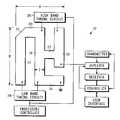
- FIG. 1is a plan view and block diagram of a tunable planar antenna and of elements connected to the antenna in a preferred embodiment of the invention
- FIG. 2is a diagrammatic plan view of the antenna of FIG. 1 in which a low band part of the antenna is indicated by solid lines;
- FIG. 3is a diagrammatic plan view of the antenna of FIG. 1 in which a high band part of the antenna is indicated by solid lines;
- FIG. 4is a schematic diagram of one example of a tuning circuit for the antenna of FIG. 1 ;
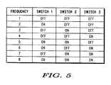
- FIG. 5is a table showing the states of the switches of FIG. 4 for eight different antenna frequencies
- FIG. 6is a plan view and schematic diagram of a tunable planar antenna and of elements connected to the antenna in a second preferred embodiment of the invention.
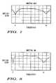
- FIG. 7is a graph of frequency versus return loss for the embodiment of FIG. 5 in a state when the switch is open;
- FIG. 8is a graph of frequency versus return loss for the embodiment of FIG. 5 in a state when the switch is closed;
- FIG. 9is a plan view of a two dimensional antenna of another embodiment.
- FIG. 10is a plan view of a two dimensional antenna of another embodiment
- FIG. 11is a plan view of a two dimensional antenna of a further embodiment.
- FIG. 12is a plan view of a two dimensional antenna of a further embodiment.
- the present disclosureconcerns a wireless communication device that has a planar, tunable antenna.
- the antennais designed such that it resonates at two different center frequencies simultaneously, which permits simultaneous operation of the device at two different frequencies. That is, reception or transmission of RF signals may be performed at two different frequencies simultaneously.
- tuning circuitscan change one or both of the two center frequencies at which the antenna resonates. Therefore, the device can operate at multiple frequencies. This allows, for example, international travelers to use cellular handsets in various regions having differing transmission standards. Further, it allows a user in one region to use multiple services with the same antenna. For example, the same antenna that is used for voice communication might also be used for receiving global positioning, or GPS, signals.
- the antennais relatively small and can be easily hidden within the housing of a portable handset.
- the wireless device, the antenna, and the method of tuning the antenna of the wireless device discussed beloware intended to and will alleviate problems caused by prior art wireless devices. It is expected that one of ordinary skill, given the described principles, concepts and examples will be able to implement other similar procedures and configurations. It is anticipated that the claims below cover such other examples.
- a wireless device 10includes a two-dimensional inverted-F antenna 12 , which is sometimes referred to as a planar inverted-F antenna, or PIFA.
- the word “planar”does not mean that the antenna must lie in a plane while in use.
- the antenna 12may be curved to conform to the body of a handset housing, for example.
- the antennais also sometimes referred to as a folded inverted-F antenna, since the leftmost element is thought of as being folded to reduce the length of the antenna.
- the antenna 12is made of conductive material such as metal.
- the antenna 12may be etched from a thin copper layer formed on a printed circuit board, for example, and tuning circuitry for tuning the antenna 12 may or may not be included on the same circuit board.
- the antennamay be applied to the inside of a handset or other wireless device such that it is out of sight to users.
- the antenna 12is generally formed by two dimensional, elements that are joined together.
- the antenna 12has a first longitudinal element 14 , a second longitudinal element 16 , and a third longitudinal element 18 , as shown.
- the first longitudinal element 14is spaced apart from the second longitudinal element 16
- the third longitudinal element 18is spaced apart from the second longitudinal element 16 .
- Connected to the longitudinal elementsare a first lateral element 20 , a second lateral element 22 , and a third lateral element 24 , which are spaced apart from one another, as shown.
- the end of the antenna at which a high band tuning circuit 36 is connectedis referred to as the upper end of the antenna for discussion purposes only and is not necessarily located in an upward position in an actual device.
- the first lateral element 20joins the first longitudinal element 14 to the second longitudinal element 16 .
- the second lateral element 22joins the second longitudinal element 16 to the third longitudinal element 18 .
- the third lateral element 24extends from the lower end of the second longitudinal element 16 as shown.
- the elements of the antenna 12form a low band element 26 directly coupled to a high band element 28 , as shown in FIGS. 2 and 3 .
- the low band element 26is simultaneously resonant at a lower frequency than the high band element 28 .
- the antenna 12is resonant at two different center frequencies, which allows operation in two bands simultaneously.
- the low band element 26 and the high band element 28share a common RF input point, which is located at the lower end of the third longitudinal element 18 and which is connected to a duplexer, as shown in FIG. 1 .
- the duplexeris connected to a transmitter and a receiver. Both the transmitter and the receiver are connected to a controller, and the controller is connected to a user interface.
- the wireless device 10includes other elements, such as a microphone and a speaker, which are not illustrated for the sake of simplicity.
- the antenna 12 of this embodimenthas the high and low band elements 26 , 28 and thus has two resonant center frequencies and thus permits operation of the device 10 at two frequencies simultaneously.
- the antenna of the device 10may have more than two elements and may have more than two simultaneous resonant frequencies.
- the corner formed by the first longitudinal element 14 and the first lateral element 20is beveled to reduce power losses in RF signal propagation.
- Other cornersmay be similarly beveled or otherwise shaped to reduce power losses.
- A, B and C in FIG. 1represent the dimensions of the antenna 12 .
- the lateral spacing between the longitudinal elements 14 , 16 , 18is approximately 5 mm, which is not considered to be a critical dimension but is preferred.
- the low band element 26is connected to a low band tuning circuit 38 . That is, one terminal of the low band tuning circuit 38 is connected to a predetermined point on the lower end of the first longitudinal element 14 of the low band element 26 , and another terminal of the low band tuning circuit 38 is connected to a predetermined point on the lower end of the second longitudinal element 16 , which is also part of the low band element 26 .
- the high band tuning circuit 38is connected to both the high band element 28 and the low band element 26 . That is, one terminal of the high band tuning circuit 38 is connected to a predetermined point on the upper end of the second longitudinal element 16 , which is part of the low band element 26 , and another terminal of the high band tuning circuit 38 is connected to a predetermined point on the third longitudinal element 18 , which is part of the high band element 28 .
- the high band tuning circuit 36 and the low band tuning circuit 38electronically alter the frequencies at which the elements 26 , 28 resonate. This can be accomplished in many ways, one of which is to selectively couple a reactance or multiple stages of reactance between elements of the antenna, as disclosed more specifically in the second and third embodiments.
- the reactanceis preferable a capacitive reactance, but may be a combination of a capacitive reactance and an inductive reactance.
- a processor or controllercan be connected to the high and low band tuning circuits 36 , 38 to independently control the high and low band tuning circuits to tune the antenna 12 to multiple pairs of high band and low band frequencies. Therefore, at any given time, the antenna is resonant at two frequencies, but those two frequencies may each be changed by the respective tuning circuits 36 , 38 and the associated controller to provide numerous different frequency pairs at which the antenna is resonant.
- FIG. 4shows a high band tuning circuit 40 of a second embodiment of the wireless communication device.
- the high band tuning circuit 40is one example of a circuit that can be employed as the high band tuning circuit 36 in FIG. 1 .
- the low band tuning circuit 38may be essentially the same as the high band tuning circuit.
- the high band tuning circuit 40includes three capacitors 62 , 64 , 68 , which are connected in a parallel manner between two predetermined points on the antenna 12 .
- each capacitor 62 , 64 , 68is a PIN diode 54 , 56 , 58 .
- Each PIN diode 54 , 56 , 58is forwardly biased by the closure of a corresponding switch 48 , 50 , 52 .
- transistorswould most likely form the switches 48 , 50 , 52 .
- Other elements of the circuit 40serve to reverse bias each PIN diodes 54 , 56 , 58 when the corresponding switch 48 , 50 , 52 is open in a manner well understood by those skilled in the art.
- each capacitor 62 , 64 , 68effectively alters the electrical length of the high band element, in this case, thus changing the center frequency at which the high band element is resonant.
- each of the capacitors 62 , 64 , 68may be connected in parallel or in series with an inductor.
- the tuning circuitcouples a reactance, which may be capacitive or a combination of a capacitive and inductive reactance, to the antenna to alter the center resonant frequency.
- PIN diodesare employed as a switching device in the embodiment of FIG. 4
- switching devicesother than PIN diodes may be employed.
- a high Q resonant switching circuitis desired in order to provide good tuning selectivity and low loss.
- the ideal switching device for this purposewould have very low ON resistance, very high isolation properties in the OFF state, and would be completely linear throughout the desired frequency range.
- RF switching devicescould be adapted for use in the tuning circuit. Examples of such devices are: MicroElectroMechanical Systems (MEMS), voltage variable capacitors (VVCs), and pseudomorphic high electron mobility transistors (PHEMTs).
- MEMSMicroElectroMechanical Systems
- VVCsvoltage variable capacitors
- PHEMTspseudomorphic high electron mobility transistors
- a local controller 60independently controls the switches 48 , 50 , 52 .
- the local controller 60is connected another controller such as a main controller.
- the local controller 60is, for example, a digital signal processor, or DSP. Input signals from the main controller indicate to the local controller 60 which of the switches 48 , 50 , 52 should be open and which should be closed, and the local controller 60 produces the required output to actuate the switches accordingly. Therefore, any combination of the states of the switches 48 , 50 , 52 can be produced.
- the capacitance of the first capacitoris less than that of the second capacitor 64
- the capacitance of the second capacitor 64is less than that of the third capacitor 68 .
- the table of FIG. 5shows that eight different resonant center frequencies of the high band element can be provided by different combinations of the states of the switches 48 , 50 , 52 .
- Adding capacitance to the tuning circuit 40that is, adding capacitance between the predetermined points of the antenna 12 , lowers the resonant center frequency of the associated element 28 . Therefore, frequency 2 in the table is lower than frequency 1 , and frequency 3 is lower than frequency 2 . Choosing the capacitance of the capacitors depends upon the antenna being used and the specifications of the desired application and thus must be determined experimentally.
- a tuning circuit identical to that of FIG. 4can also be employed as the low band tuning circuit 38 of FIG. 1 , many different frequency combinations can be produced, allowing the wireless communication device 10 to operate at many different pairs of frequencies.
- Changing the center resonant frequency of one of the band elements 26 , 28can be accomplished by sending a signal to the local controller 60 , so frequency changes are rapid.
- the high band tuning circuit and the low band tuning circuitare controlled independently in the embodiment of FIG. 4 .
- the resonant frequency of the high band element 28can be changed without changing the resonant frequency of the low band element 26 if desired.
- a single local controller 60can control the capacitance stages of both the high band tuning circuit and the low band tuning circuit.
- FIG. 6shows a wireless communication device 70 of a third embodiment.
- the device 70is quad-banded. That is, it operates in two bands simultaneously, that is, it has two resonant center frequencies.
- a controller or processorcan change the state of the switch 78 .
- the high band element 28 and the low band element 26are tuned in unison, not independently.
- the device 70includes a high band tuning circuit, which is connected to the second longitudinal element 16 and the third longitudinal element 18 , as shown.
- a low band tuning circuitis connected to the second longitudinal element 16 and the first longitudinal element 14 .
- a capacitor 74is connected between two predetermined points on the antenna 12 in the high band tuning circuit.
- a capacitor 80is connected between two predetermined points on the antenna 12 in the low band tuning circuit.
- Each capacitor 82 , 80has a corresponding PIN diode 74 , 76 in series.
- the switch 78When the switch 78 is closed, the PIN diodes 74 , 76 are in a conducting state and couple the capacitors 80 , 82 between the respective pairs of predetermined points on the antenna 12 . This alters the center resonant frequencies of both the high band element 28 and the low band element 26 simultaneously, which allows the device 70 to operate at a different pair of frequencies.
- the switch 78When the switch 78 is open, the PIN diodes 74 , 76 are in a non-conducting state and remove the capacitances of the capacitors 80 , 82 between the respective pairs of predetermined points on the antenna 12 . In other words, opening the switch 78 is an attempt to create an open circuit at the PIN diodes 74 , 76 .
- FIG. 7is a return loss graph for the antenna 12 of the device 70 of FIG. 6 when the switch 78 is open, or off.
- the vertical axishas a logarithmic scale.
- the plotshows two center frequencies A, B, at which the antenna resonates.
- Frequency Athe low band frequency
- frequency Bthe high band frequency
- is approximately 1.9 GHzwhich is a frequency used for wireless communication in the U.S.
- FIG. 8shows a similar return loss plot taken with the switch 78 in the on, or closed, state in the device of FIG. 6 .
- the vertical axishas a logarithmic scale.
- two center frequencies C, Dappear.
- Frequency Cthe low band frequency
- frequency Dthe high band frequency
- is approximately 1.8 GHzwhich is a frequency used for wireless communication in Europe.
- FIGS. 9-12show various configurations of the antenna.
- Each of the antennas of FIGS. 9-12has a low band element 110 , a high band element 108 , a first high band predetermined point 100 , at which one terminal of the high band tuning circuit 36 is connected, a second high band predetermined point 102 , at which the other terminal of the high band tuning circuit 36 is connected, a first low band predetermined point 104 , at which one terminal of the low band tuning circuit 36 is connected, a second low band predetermined point 106 , at which the other terminal of the low band tuning circuit 36 is connected, and an RF input point 98 , which is connected to the duplexer or similar component of the wireless communication device.
- FIGS. 9-12illustrate that many variations in shape of the antenna 12 are possible.
Landscapes
- Engineering & Computer Science (AREA)
- Computer Networks & Wireless Communication (AREA)
- Waveguide Aerials (AREA)
- Variable-Direction Aerials And Aerial Arrays (AREA)
- Transceivers (AREA)
Abstract
Description
Claims (20)
Priority Applications (1)
| Application Number | Priority Date | Filing Date | Title |
|---|---|---|---|
| US10/330,155US6933893B2 (en) | 2002-12-27 | 2002-12-27 | Electronically tunable planar antenna and method of tuning the same |
Applications Claiming Priority (1)
| Application Number | Priority Date | Filing Date | Title |
|---|---|---|---|
| US10/330,155US6933893B2 (en) | 2002-12-27 | 2002-12-27 | Electronically tunable planar antenna and method of tuning the same |
Publications (2)
| Publication Number | Publication Date |
|---|---|
| US20040125027A1 US20040125027A1 (en) | 2004-07-01 |
| US6933893B2true US6933893B2 (en) | 2005-08-23 |
Family
ID=32654435
Family Applications (1)
| Application Number | Title | Priority Date | Filing Date |
|---|---|---|---|
| US10/330,155Expired - LifetimeUS6933893B2 (en) | 2002-12-27 | 2002-12-27 | Electronically tunable planar antenna and method of tuning the same |
Country Status (1)
| Country | Link |
|---|---|
| US (1) | US6933893B2 (en) |
Cited By (16)
| Publication number | Priority date | Publication date | Assignee | Title |
|---|---|---|---|---|
| US20040192226A1 (en)* | 2003-03-31 | 2004-09-30 | Motorola, Inc. | Miniature vertically polarized multiple frequency band antenna and method of providing an antenna for a wireless device |
| US20050162324A1 (en)* | 2004-01-26 | 2005-07-28 | Kyocera Corporation | Antenna using variable capacitance element and wireless communication apparatus using the same |
| US20060293097A1 (en)* | 2004-03-04 | 2006-12-28 | Murata Manufacturing Co., Ltd. | Antenna device and radio communication apparatus using the same |
| US20080055164A1 (en)* | 2006-09-05 | 2008-03-06 | Zhijun Zhang | Tunable antennas for handheld devices |
| US20080122712A1 (en)* | 2006-11-28 | 2008-05-29 | Agile Rf, Inc. | Tunable antenna including tunable capacitor inserted inside the antenna |
| US20090051595A1 (en)* | 2007-08-23 | 2009-02-26 | Research In Motion Limited | Multi-band antenna, and associated methodology, for a radio communication device |
| US20100022203A1 (en)* | 2008-03-07 | 2010-01-28 | Stmicroelectronics (Tours) Sas | Circuit integrating a tunable antenna with a standing wave rate correction |
| US20100026596A1 (en)* | 2008-07-31 | 2010-02-04 | Kabushiki Kaisha Toshiba | Antenna device |
| US20100302106A1 (en)* | 2009-05-29 | 2010-12-02 | Infineon Technologies Ag | Impedance Tuning of Transmitting and Receiving Antennas |
| US20110102282A1 (en)* | 2009-11-02 | 2011-05-05 | Industrial Technology Research Institute | Reconfigurable multi-band antenna system and electronic apparatus having the same |
| CN102055071A (en)* | 2009-11-04 | 2011-05-11 | 财团法人工业技术研究院 | Reconfigurable multi-frequency antenna system and its electronic device |
| WO2012092198A1 (en)* | 2010-12-28 | 2012-07-05 | Lockheed Martin Corporation | Safe area voltage and current interface |
| US9293828B2 (en) | 2013-03-27 | 2016-03-22 | Apple Inc. | Antenna system with tuning from coupled antenna |
| US9444130B2 (en) | 2013-04-10 | 2016-09-13 | Apple Inc. | Antenna system with return path tuning and loop element |
| US9559433B2 (en) | 2013-03-18 | 2017-01-31 | Apple Inc. | Antenna system having two antennas and three ports |
| US10355339B2 (en) | 2013-03-18 | 2019-07-16 | Apple Inc. | Tunable antenna with slot-based parasitic element |
Families Citing this family (22)
| Publication number | Priority date | Publication date | Assignee | Title |
|---|---|---|---|---|
| US8744384B2 (en) | 2000-07-20 | 2014-06-03 | Blackberry Limited | Tunable microwave devices with auto-adjusting matching circuit |
| US7307591B2 (en)* | 2004-07-20 | 2007-12-11 | Nokia Corporation | Multi-band antenna |
| WO2006034940A1 (en)* | 2004-09-27 | 2006-04-06 | Fractus, S.A. | Tunable antenna |
| US7711337B2 (en) | 2006-01-14 | 2010-05-04 | Paratek Microwave, Inc. | Adaptive impedance matching module (AIMM) control architectures |
| US7535312B2 (en) | 2006-11-08 | 2009-05-19 | Paratek Microwave, Inc. | Adaptive impedance matching apparatus, system and method with improved dynamic range |
| US7714676B2 (en) | 2006-11-08 | 2010-05-11 | Paratek Microwave, Inc. | Adaptive impedance matching apparatus, system and method |
| US8583065B2 (en)* | 2007-06-07 | 2013-11-12 | Vishay Intertechnology, Inc. | Digitally controlled antenna tuning circuit for radio frequency receivers |
| US7991363B2 (en) | 2007-11-14 | 2011-08-02 | Paratek Microwave, Inc. | Tuning matching circuits for transmitter and receiver bands as a function of transmitter metrics |
| GB0817237D0 (en)* | 2008-09-22 | 2008-10-29 | Antenova Ltd | Tuneable antennas suitable for portable digitial television receivers |
| US9026062B2 (en) | 2009-10-10 | 2015-05-05 | Blackberry Limited | Method and apparatus for managing operations of a communication device |
| US8803631B2 (en) | 2010-03-22 | 2014-08-12 | Blackberry Limited | Method and apparatus for adapting a variable impedance network |
| JP5901612B2 (en) | 2010-04-20 | 2016-04-13 | ブラックベリー リミテッド | Method and apparatus for managing interference in a communication device |
| US8712340B2 (en) | 2011-02-18 | 2014-04-29 | Blackberry Limited | Method and apparatus for radio antenna frequency tuning |
| CA2836419C (en)* | 2011-05-16 | 2016-11-29 | Gregory MENDOLIA | Method and apparatus for tuning a communication device |
| US8594584B2 (en) | 2011-05-16 | 2013-11-26 | Blackberry Limited | Method and apparatus for tuning a communication device |
| EP2740221B1 (en) | 2011-08-05 | 2019-06-26 | BlackBerry Limited | Method and apparatus for band tuning in a communication device |
| US9853363B2 (en) | 2012-07-06 | 2017-12-26 | Blackberry Limited | Methods and apparatus to control mutual coupling between antennas |
| US9350405B2 (en) | 2012-07-19 | 2016-05-24 | Blackberry Limited | Method and apparatus for antenna tuning and power consumption management in a communication device |
| US10404295B2 (en) | 2012-12-21 | 2019-09-03 | Blackberry Limited | Method and apparatus for adjusting the timing of radio antenna tuning |
| US9455501B2 (en)* | 2013-06-24 | 2016-09-27 | Galtronics Corporation, Ltd. | Broadband multiple-input multiple-output antenna |
| US9438319B2 (en) | 2014-12-16 | 2016-09-06 | Blackberry Limited | Method and apparatus for antenna selection |
| US11757191B2 (en)* | 2021-06-28 | 2023-09-12 | Dell Products L.P. | Dynamic antenna structure tuning mechanism |
Citations (7)
| Publication number | Priority date | Publication date | Assignee | Title |
|---|---|---|---|---|
| US5969681A (en)* | 1998-06-05 | 1999-10-19 | Ericsson Inc. | Extended bandwidth dual-band patch antenna systems and associated methods of broadband operation |
| US6140966A (en)* | 1997-07-08 | 2000-10-31 | Nokia Mobile Phones Limited | Double resonance antenna structure for several frequency ranges |
| US6175334B1 (en)* | 1997-05-09 | 2001-01-16 | Motorola, Inc. | Difference drive diversity antenna structure and method |
| US6268831B1 (en) | 2000-04-04 | 2001-07-31 | Ericsson Inc. | Inverted-f antennas with multiple planar radiating elements and wireless communicators incorporating same |
| US20020044091A1 (en) | 2000-10-18 | 2002-04-18 | Filtronic Lk Oy | Double-action antenna |
| US6509881B2 (en)* | 2000-07-10 | 2003-01-21 | Telefonaktielbolaget Lm Ericsson (Publ) | One aperture simultaneous RX-TX-antenna |
| US6650295B2 (en)* | 2002-01-28 | 2003-11-18 | Nokia Corporation | Tunable antenna for wireless communication terminals |
- 2002
- 2002-12-27USUS10/330,155patent/US6933893B2/ennot_activeExpired - Lifetime
Patent Citations (7)
| Publication number | Priority date | Publication date | Assignee | Title |
|---|---|---|---|---|
| US6175334B1 (en)* | 1997-05-09 | 2001-01-16 | Motorola, Inc. | Difference drive diversity antenna structure and method |
| US6140966A (en)* | 1997-07-08 | 2000-10-31 | Nokia Mobile Phones Limited | Double resonance antenna structure for several frequency ranges |
| US5969681A (en)* | 1998-06-05 | 1999-10-19 | Ericsson Inc. | Extended bandwidth dual-band patch antenna systems and associated methods of broadband operation |
| US6268831B1 (en) | 2000-04-04 | 2001-07-31 | Ericsson Inc. | Inverted-f antennas with multiple planar radiating elements and wireless communicators incorporating same |
| US6509881B2 (en)* | 2000-07-10 | 2003-01-21 | Telefonaktielbolaget Lm Ericsson (Publ) | One aperture simultaneous RX-TX-antenna |
| US20020044091A1 (en) | 2000-10-18 | 2002-04-18 | Filtronic Lk Oy | Double-action antenna |
| US6650295B2 (en)* | 2002-01-28 | 2003-11-18 | Nokia Corporation | Tunable antenna for wireless communication terminals |
Non-Patent Citations (3)
| Title |
|---|
| Liu, Hall and Wake; "Dual-Frequency Planar Inverted-F Antenna"; IEEE Transactions on Antennas and Propagation, vol. 45, No. 10, Oct. 1997; pp. 1451-1458. |
| Song, Hall, Ghafouri-Shiraz and Wake; "Triple-Band Planar Inverted F Antenna"; 1999 IEEE; pp. 908-911. |
| Yajun and Kwang; "One Novel Single-Patch Dual-Frequency Planar Inverted-F Antenna"; 2000 IEEE 2nd Int'l Conf on Microwave and Millimeter Wave Tech Proceedings; pp. 444-447. |
Cited By (30)
| Publication number | Priority date | Publication date | Assignee | Title |
|---|---|---|---|---|
| US20040192226A1 (en)* | 2003-03-31 | 2004-09-30 | Motorola, Inc. | Miniature vertically polarized multiple frequency band antenna and method of providing an antenna for a wireless device |
| US7369086B2 (en)* | 2003-03-31 | 2008-05-06 | Freescale Semiconductor, Inc. | Miniature vertically polarized multiple frequency band antenna and method of providing an antenna for a wireless device |
| US20050162324A1 (en)* | 2004-01-26 | 2005-07-28 | Kyocera Corporation | Antenna using variable capacitance element and wireless communication apparatus using the same |
| US7109944B2 (en)* | 2004-01-26 | 2006-09-19 | Kyocera Corporation | Antenna using variable capacitance element and wireless communication apparatus using the same |
| US7502638B2 (en)* | 2004-03-04 | 2009-03-10 | Murata Manufacturing Co., Ltd. | Antenna device and radio communication apparatus using the same |
| US20060293097A1 (en)* | 2004-03-04 | 2006-12-28 | Murata Manufacturing Co., Ltd. | Antenna device and radio communication apparatus using the same |
| US20080055164A1 (en)* | 2006-09-05 | 2008-03-06 | Zhijun Zhang | Tunable antennas for handheld devices |
| US7671804B2 (en) | 2006-09-05 | 2010-03-02 | Apple Inc. | Tunable antennas for handheld devices |
| US20080122712A1 (en)* | 2006-11-28 | 2008-05-29 | Agile Rf, Inc. | Tunable antenna including tunable capacitor inserted inside the antenna |
| US20090051595A1 (en)* | 2007-08-23 | 2009-02-26 | Research In Motion Limited | Multi-band antenna, and associated methodology, for a radio communication device |
| US7719470B2 (en)* | 2007-08-23 | 2010-05-18 | Research In Motion Limited | Multi-band antenna, and associated methodology, for a radio communication device |
| US20100022203A1 (en)* | 2008-03-07 | 2010-01-28 | Stmicroelectronics (Tours) Sas | Circuit integrating a tunable antenna with a standing wave rate correction |
| US8412121B2 (en)* | 2008-03-07 | 2013-04-02 | Stmicroelectronics (Tours) Sas | Circuit integrating a tunable antenna with a standing wave rate correction |
| US20100026596A1 (en)* | 2008-07-31 | 2010-02-04 | Kabushiki Kaisha Toshiba | Antenna device |
| US20100302106A1 (en)* | 2009-05-29 | 2010-12-02 | Infineon Technologies Ag | Impedance Tuning of Transmitting and Receiving Antennas |
| US9225380B2 (en) | 2009-05-29 | 2015-12-29 | Intel Mobile Communications GmbH | Semiconductor device and fabrication method |
| US8928536B2 (en)* | 2009-05-29 | 2015-01-06 | Intel Corporation | Impedance tuning of transmitting and receiving antennas |
| US8232925B2 (en)* | 2009-05-29 | 2012-07-31 | Intel Mobile Communications GmbH | Impedance tuning of transmitting and receiving antennas |
| US20120293384A1 (en)* | 2009-05-29 | 2012-11-22 | Mikael Bergholz Knudsen | Impedance tuning of transmitting and receiving antennas |
| US20110102282A1 (en)* | 2009-11-02 | 2011-05-05 | Industrial Technology Research Institute | Reconfigurable multi-band antenna system and electronic apparatus having the same |
| CN102055071B (en)* | 2009-11-04 | 2013-11-13 | 财团法人工业技术研究院 | Reconfigurable multi-frequency antenna system and its electronic device |
| CN102055071A (en)* | 2009-11-04 | 2011-05-11 | 财团法人工业技术研究院 | Reconfigurable multi-frequency antenna system and its electronic device |
| US8351879B2 (en) | 2010-12-28 | 2013-01-08 | Lockheed Martin Corporation | Safe area voltage and current interface |
| CN103261990A (en)* | 2010-12-28 | 2013-08-21 | 洛克希德马丁公司 | Safe area voltage and current interface |
| WO2012092198A1 (en)* | 2010-12-28 | 2012-07-05 | Lockheed Martin Corporation | Safe area voltage and current interface |
| CN103261990B (en)* | 2010-12-28 | 2016-06-08 | 洛克希德马丁公司 | Safety zone voltage and current interface |
| US9559433B2 (en) | 2013-03-18 | 2017-01-31 | Apple Inc. | Antenna system having two antennas and three ports |
| US10355339B2 (en) | 2013-03-18 | 2019-07-16 | Apple Inc. | Tunable antenna with slot-based parasitic element |
| US9293828B2 (en) | 2013-03-27 | 2016-03-22 | Apple Inc. | Antenna system with tuning from coupled antenna |
| US9444130B2 (en) | 2013-04-10 | 2016-09-13 | Apple Inc. | Antenna system with return path tuning and loop element |
Also Published As
| Publication number | Publication date |
|---|---|
| US20040125027A1 (en) | 2004-07-01 |
Similar Documents
| Publication | Publication Date | Title |
|---|---|---|
| US6933893B2 (en) | Electronically tunable planar antenna and method of tuning the same | |
| US9685698B2 (en) | Multi-tap frequency switchable antenna apparatus, systems and methods | |
| EP1290757B1 (en) | Convertible dipole/inverted-f antennas and wireless communicators incorporating the same | |
| US6662028B1 (en) | Multiple frequency inverted-F antennas having multiple switchable feed points and wireless communicators incorporating the same | |
| US6700540B2 (en) | Antennas having multiple resonant frequency bands and wireless terminals incorporating the same | |
| EP1295358B1 (en) | Convertible loop/inverted-f antennas and wireless communicators incorporating the same | |
| US6198442B1 (en) | Multiple frequency band branch antennas for wireless communicators | |
| AU719362B2 (en) | Planar antenna | |
| US7760146B2 (en) | Internal digital TV antennas for hand-held telecommunications device | |
| US6950065B2 (en) | Mobile communication device | |
| US6515625B1 (en) | Antenna | |
| EP1248317A1 (en) | Electrically tunable multiband planar antenna | |
| JP2004505581A (en) | An antenna with a flat radiating surface and a mobile phone equipped with this antenna | |
| US7102575B2 (en) | PIFA antenna apparatus for mobile communications terminals | |
| WO2001008260A1 (en) | Flat dual frequency band antennas for wireless communicators | |
| JP2000114856A (en) | Reversed f antenna and radio equipment using the same | |
| JP3430140B2 (en) | Inverted-F antenna and wireless device using the same | |
| EP1595308A2 (en) | Electronically tunable quad-band antennas for handset applications | |
| US6314276B1 (en) | Transmitted-receiver | |
| KR100872249B1 (en) | System and method for dual-band antenna matching | |
| WO2006127528A1 (en) | Selectable length meander line antenna | |
| US7928914B2 (en) | Multi-frequency conductive-strip antenna system | |
| US11949438B2 (en) | Multi-band antenna for use with limited size ground planes | |
| WO2004097976A3 (en) | Tuneable antenna | |
| JP2003078315A (en) | Telescopic antenna |
Legal Events
| Date | Code | Title | Description |
|---|---|---|---|
| AS | Assignment | Owner name:MOTOROLA, INC., ILLINOIS Free format text:ASSIGNMENT OF ASSIGNORS INTEREST;ASSIGNORS:RUBINSHTEYN, BORIS;SCHEER, ROGER L.;REEL/FRAME:013641/0684 Effective date:20021226 | |
| STCF | Information on status: patent grant | Free format text:PATENTED CASE | |
| CC | Certificate of correction | ||
| FPAY | Fee payment | Year of fee payment:4 | |
| AS | Assignment | Owner name:MOTOROLA MOBILITY, INC, ILLINOIS Free format text:ASSIGNMENT OF ASSIGNORS INTEREST;ASSIGNOR:MOTOROLA, INC;REEL/FRAME:025673/0558 Effective date:20100731 | |
| AS | Assignment | Owner name:MOTOROLA MOBILITY LLC, ILLINOIS Free format text:CHANGE OF NAME;ASSIGNOR:MOTOROLA MOBILITY, INC.;REEL/FRAME:029216/0282 Effective date:20120622 | |
| FPAY | Fee payment | Year of fee payment:8 | |
| AS | Assignment | Owner name:GOOGLE TECHNOLOGY HOLDINGS LLC, CALIFORNIA Free format text:ASSIGNMENT OF ASSIGNORS INTEREST;ASSIGNOR:MOTOROLA MOBILITY LLC;REEL/FRAME:034449/0001 Effective date:20141028 | |
| FPAY | Fee payment | Year of fee payment:12 |