US6933786B1 - Amplifier circuit and method - Google Patents
Amplifier circuit and methodDownload PDFInfo
- Publication number
- US6933786B1 US6933786B1US10/146,524US14652402AUS6933786B1US 6933786 B1US6933786 B1US 6933786B1US 14652402 AUS14652402 AUS 14652402AUS 6933786 B1US6933786 B1US 6933786B1
- Authority
- US
- United States
- Prior art keywords
- amplifier
- circuit
- gain
- controllable
- input impedance
- Prior art date
- Legal status (The legal status is an assumption and is not a legal conclusion. Google has not performed a legal analysis and makes no representation as to the accuracy of the status listed.)
- Expired - Lifetime
Links
Images

Classifications
- H—ELECTRICITY
- H03—ELECTRONIC CIRCUITRY
- H03F—AMPLIFIERS
- H03F1/00—Details of amplifiers with only discharge tubes, only semiconductor devices or only unspecified devices as amplifying elements
- H03F1/56—Modifications of input or output impedances, not otherwise provided for
- H—ELECTRICITY
- H03—ELECTRONIC CIRCUITRY
- H03F—AMPLIFIERS
- H03F3/00—Amplifiers with only discharge tubes or only semiconductor devices as amplifying elements
- H03F3/04—Amplifiers with only discharge tubes or only semiconductor devices as amplifying elements with semiconductor devices only
- H03F3/08—Amplifiers with only discharge tubes or only semiconductor devices as amplifying elements with semiconductor devices only controlled by light
- H03F3/087—Amplifiers with only discharge tubes or only semiconductor devices as amplifying elements with semiconductor devices only controlled by light with IC amplifier blocks
- H—ELECTRICITY
- H03—ELECTRONIC CIRCUITRY
- H03F—AMPLIFIERS
- H03F3/00—Amplifiers with only discharge tubes or only semiconductor devices as amplifying elements
- H03F3/45—Differential amplifiers
- H03F3/45071—Differential amplifiers with semiconductor devices only
- H03F3/45076—Differential amplifiers with semiconductor devices only characterised by the way of implementation of the active amplifying circuit in the differential amplifier
- H03F3/4508—Differential amplifiers with semiconductor devices only characterised by the way of implementation of the active amplifying circuit in the differential amplifier using bipolar transistors as the active amplifying circuit
- H03F3/45085—Long tailed pairs
- H—ELECTRICITY
- H03—ELECTRONIC CIRCUITRY
- H03F—AMPLIFIERS
- H03F3/00—Amplifiers with only discharge tubes or only semiconductor devices as amplifying elements
- H03F3/45—Differential amplifiers
- H03F3/45071—Differential amplifiers with semiconductor devices only
- H03F3/45076—Differential amplifiers with semiconductor devices only characterised by the way of implementation of the active amplifying circuit in the differential amplifier
- H03F3/45475—Differential amplifiers with semiconductor devices only characterised by the way of implementation of the active amplifying circuit in the differential amplifier using IC blocks as the active amplifying circuit
- H—ELECTRICITY
- H03—ELECTRONIC CIRCUITRY
- H03G—CONTROL OF AMPLIFICATION
- H03G1/00—Details of arrangements for controlling amplification
- H03G1/0005—Circuits characterised by the type of controlling devices operated by a controlling current or voltage signal
- H03G1/0035—Circuits characterised by the type of controlling devices operated by a controlling current or voltage signal using continuously variable impedance elements
- H03G1/007—Circuits characterised by the type of controlling devices operated by a controlling current or voltage signal using continuously variable impedance elements using field-effect transistors [FET]
- H—ELECTRICITY
- H03—ELECTRONIC CIRCUITRY
- H03G—CONTROL OF AMPLIFICATION
- H03G1/00—Details of arrangements for controlling amplification
- H03G1/0005—Circuits characterised by the type of controlling devices operated by a controlling current or voltage signal
- H03G1/0088—Circuits characterised by the type of controlling devices operated by a controlling current or voltage signal using discontinuously variable devices, e.g. switch-operated
- H—ELECTRICITY
- H03—ELECTRONIC CIRCUITRY
- H03F—AMPLIFIERS
- H03F2200/00—Indexing scheme relating to amplifiers
- H03F2200/222—A circuit being added at the input of an amplifier to adapt the input impedance of the amplifier
- H—ELECTRICITY
- H03—ELECTRONIC CIRCUITRY
- H03F—AMPLIFIERS
- H03F2203/00—Indexing scheme relating to amplifiers with only discharge tubes or only semiconductor devices as amplifying elements covered by H03F3/00
- H03F2203/45—Indexing scheme relating to differential amplifiers
- H03F2203/45702—Indexing scheme relating to differential amplifiers the LC comprising two resistors
Definitions
- the present inventionrelates generally to the field of electronics and more particularly to an amplifier circuit and method.
- Amplifiersare used in numerous electronic circuits.
- One challenging environmentis the amplification of the output of a photodiode or optical detector.
- the amplifier circuitis used to convert the current signal from the photodiode into a voltage signal.
- the currentmay have a wide dynamic range due to the variations in the input optical power.
- the amplifier circuitmust accommodate a wide dynamic range.
- the prior art solutionsgenerally use a trans-impedance amplifier and associated circuitry that changes the input impedance and the gain of the overall circuit. These solutions have the beneficial effect of being able to deal with the wide dynamic range.
- the variation in the input impedanceresult in different frequency responses for different gain settings. This results in inaccuracies in the amplified waveform.
- An amplifier systemthat overcomes these problems has a control circuit.
- An amplifieris coupled to the control circuit and has a controllable gain.
- a controllable input impedance circuitis coupled to the control circuit. When the gain of the amplifier is changed the controllable input impedance circuit's impedance is adjusted, so that the input impedance to the system remains essentially constant.
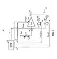
- FIG. 1is a block and schematic diagram of an amplifier system in accordance with one embodiment of the invention
- FIG. 2is a schematic diagram of the amplifier of FIG. 1 in accordance with one embodiment of the invention.
- FIG. 3is a schematic diagram of the amplifier of FIG. 1 in accordance with one embodiment of the invention.
- FIG. 4is a schematic diagram of the amplifier of FIG. 1 in accordance with one embodiment of the invention.
- FIG. 1is a block and schematic diagram of an amplifier system 10 in accordance with one embodiment of the invention.
- a photodiode 12is shown coupled to the amplifier system 10 .
- the amplifier system 10detects a voltage range of the output 14 of the photodiode 12 at a control circuit 16 .
- the control circuit 16controls a gain (controllable gain) of an amplifier (trans-impedance amplifier, open loop amplifier) 18 and a controllable input impedance circuit 20 .
- the control circuit 16can select between a first range 22 and a second range 24 .
- the controllable input impedance circuit 20is formed by a variable feedback resistance.
- the variable feedback resistancein the embodiment shown, has a first resistor 26 in series with a first switch 28 .
- the first switch 28is controlled by the control circuit 16 .
- the variable feedback resistancealso has a second resistor 30 in series with a second switch 32 .
- the first resistor 26is electrically in parallel with the second resistor 30 and both resistors 26 , 30 are connected between the output 34 and the input 36 of the amplifier 18 . While the controllable input impedance circuit 20 is shown as having two (or three) settings it will be apparent to those skilled in the art how the circuit can be made to have numerous setting or perhaps a variable setting.
- the control circuit 16adjusts the open loop gain of the amplifier 18 based on the output voltage.
- the output voltageis directly related to the input current.
- the first range line 22is on the amplifier gain is A.
- the first switch 28is on (closed) and the second switch 32 is off (open).
- the input impedanceis R1/A.
- the range two line 24is turned on by the control circuit 16 .
- the gain of the amplifieris reduced to A*R2/R1.
- the second switch 32is on and the first switch 28 is off in the second range.
- the input impedanceremains R1/A (fixed input impedance).
- FIG. 2is a schematic diagram of the amplifier 18 of FIG. 1 in accordance with one embodiment of the invention.
- the amplifier 18has an amplifier 40 with an input 42 connected to a gain adjustment element (gain control circuit) 44 .
- the input 36 to the amplifier 18is connected to the base of a transistor 46 .
- the collector 48 of the transistor 46is connected to the input 42 of amplifier 40 and to a load resistor 50 .
- the other end of the load resistor 50is connected to a source voltage 52 .
- the emitter 54is connected to a current (gain) limiting resistor 56 .
- the gain adjustment resistor 56is in parallel with a switch 58 .
- the other end of the gain adjustment resistor 56is connected to ground 60 .
- the switch 58is connected to the first range control line 22 .
- the switch (transistor) 58When the first range line is on (high) the switch (transistor) 58 is closed and the gain adjustment resistor 56 is bypassed. When the second range line is on (high) and the first range line is off (low) the switch 58 is open and the current flows through the gain adjustment resistor 56 .
- FIG. 3is a schematic diagram of the amplifier 18 of FIG. 1 in accordance with one embodiment of the invention.
- the embodiment shown in FIG. 3is similar to FIG. 2 except the gain adjustment resistor 56 and associated switch 58 have been replaced with a controllable current source 62 .
- the emitter 54 of the transistor 46is connected directly to ground 60 .
- the controllable current source 62is connected to the input 42 of the amplifier 40 and has a control input connected to the second range control line 24 . When the second range line is on (high) the controllable current source 62 is on and as a result reduces the input current to the transistor 46 .
- FIG. 4is a schematic diagram of the amplifier 18 of FIG. 1 in accordance with one embodiment of the invention.
- FIG. 4is similar to FIG. 3 except that it is designed to have a differential inputs 36 a , 36 b . All the differential sections of the circuit shown in FIG. 3 are labeled “a” & “b” and have essentially the same function.
- the current sources 62 a , 62 bsupply a current of 1 ⁇ 2 *I.
- two new current sourceshave been added.
- a first controllable current source 70coupled to control line 22 and a second constant current source 72 .
- the process embodied in the circuits and systemsmay be generalized.
- the processinvolves determining an output voltage. In the embodiments shown, this is determined by the control circuit 16 .
- the feedback resistanceis determined based on the output voltage.
- An internal gain of the amplifier 18is determined based on the feedback resistance. This step may be performed by the control circuit 16 .
- the feedback resistanceis determined to produce a constant input impedance.
Landscapes
- Engineering & Computer Science (AREA)
- Power Engineering (AREA)
- Control Of Amplification And Gain Control (AREA)
- Amplifiers (AREA)
Abstract
Description
Re=(1/gm)((R1/R2)−1)
Where gm is the transconductance of
I=IL(1−R2/R1)
By selecting the current source to have this value, the relationship between the gain of the
I1=I*(R1/R2−1)
Where I is the current supplied by the second constant
Claims (20)
Priority Applications (1)
| Application Number | Priority Date | Filing Date | Title |
|---|---|---|---|
| US10/146,524US6933786B1 (en) | 2002-05-15 | 2002-05-15 | Amplifier circuit and method |
Applications Claiming Priority (1)
| Application Number | Priority Date | Filing Date | Title |
|---|---|---|---|
| US10/146,524US6933786B1 (en) | 2002-05-15 | 2002-05-15 | Amplifier circuit and method |
Publications (1)
| Publication Number | Publication Date |
|---|---|
| US6933786B1true US6933786B1 (en) | 2005-08-23 |
Family
ID=34837109
Family Applications (1)
| Application Number | Title | Priority Date | Filing Date |
|---|---|---|---|
| US10/146,524Expired - LifetimeUS6933786B1 (en) | 2002-05-15 | 2002-05-15 | Amplifier circuit and method |
Country Status (1)
| Country | Link |
|---|---|
| US (1) | US6933786B1 (en) |
Cited By (16)
| Publication number | Priority date | Publication date | Assignee | Title |
|---|---|---|---|---|
| US20050046482A1 (en)* | 2003-08-27 | 2005-03-03 | Karl Schrodinger | Receiver circuit |
| US20050168289A1 (en)* | 2004-01-30 | 2005-08-04 | Infineon Technologies Ag | Receiver circuit having an optical reception device |
| US20050169407A1 (en)* | 2004-01-30 | 2005-08-04 | Infineon Technologies Ag | Receiver circuit and a method for its operation |
| US20060087378A1 (en)* | 2004-10-26 | 2006-04-27 | Hiroshi Hayakawa | Preamplifier circuit having a variable feedback resistance |
| US20060103472A1 (en)* | 2004-11-18 | 2006-05-18 | Matsushita Electric Industrial Co., Ltd. | Light receiving amplification circuit |
| US20060226913A1 (en)* | 2003-07-30 | 2006-10-12 | Mitsubishi Denki Kabushiki Kaisha | Circuit for varying gain of preamplifier |
| US20060232339A1 (en)* | 2005-04-14 | 2006-10-19 | Demonte Frank J | Electronic amplifier with signal gain dependent bias |
| US20070075768A1 (en)* | 2005-09-30 | 2007-04-05 | Thomas Blon | Circuit configuration having a feedback operational amplifier |
| US20080088368A1 (en)* | 2006-10-17 | 2008-04-17 | Gajender Rohilla | Offset voltage correction for high gain amplifier |
| US20080258818A1 (en)* | 2007-04-20 | 2008-10-23 | Tuan Van Ngo | Amplifier with progammable input impedance |
| US20090237156A1 (en)* | 2008-03-19 | 2009-09-24 | Freescale Semiconductor, Inc. | Power amplifiers having improved startup linearization and related operating methods |
| US20150207467A1 (en)* | 2014-01-18 | 2015-07-23 | Ali Mohamed Darwish | Method and system for linearizing an amplifier using transistor-level dynamic feedback |
| US20170040954A1 (en)* | 2014-01-18 | 2017-02-09 | Ali Mohamed Darwish | Method and system for linearizing an amplifier using transistor-level dynamic feedback |
| US9628195B2 (en)* | 2014-10-22 | 2017-04-18 | Source Photonics (Chengdu) Co., Ltd. | Transimpedance amplifier (TIA) having an enlarged dynamic range and optical devices using the same |
| US10958355B2 (en)* | 2018-11-07 | 2021-03-23 | Sumitomo Electric Industries, Ltd. | Optical receiver circuit |
| US10985708B2 (en)* | 2014-03-27 | 2021-04-20 | Texas Instruments Incorporated | Time gain compensation circuit in an ultrasound receiver |
Citations (7)
| Publication number | Priority date | Publication date | Assignee | Title |
|---|---|---|---|---|
| US4563656A (en)* | 1984-11-05 | 1986-01-07 | Gte Laboratories Incorporated | Wideband transimpedance optical receiver |
| US5532471A (en)* | 1994-12-21 | 1996-07-02 | At&T Corp. | Optical transimpedance amplifier with high dynamic range |
| US5734300A (en) | 1996-05-17 | 1998-03-31 | Lucent Technologies, Inc. | Optical receiver preamplifier dynamic range enhancing circuit and method |
| US5812030A (en)* | 1995-06-20 | 1998-09-22 | Nec Corporation | Amplifier device capable of carrying out a stable amplifying operation without a gain variation |
| US6229395B1 (en)* | 1999-10-01 | 2001-05-08 | Rf Micro Devices, Inc. | Differential transconductance amplifier |
| US6246282B1 (en)* | 1998-11-05 | 2001-06-12 | Nec Corporation | First stage amplifier circuit |
| US6303922B1 (en) | 1997-07-21 | 2001-10-16 | Ortel Corporation | Range-switching optical receiver with high sensitivity and wide dynamic range |
- 2002
- 2002-05-15USUS10/146,524patent/US6933786B1/ennot_activeExpired - Lifetime
Patent Citations (7)
| Publication number | Priority date | Publication date | Assignee | Title |
|---|---|---|---|---|
| US4563656A (en)* | 1984-11-05 | 1986-01-07 | Gte Laboratories Incorporated | Wideband transimpedance optical receiver |
| US5532471A (en)* | 1994-12-21 | 1996-07-02 | At&T Corp. | Optical transimpedance amplifier with high dynamic range |
| US5812030A (en)* | 1995-06-20 | 1998-09-22 | Nec Corporation | Amplifier device capable of carrying out a stable amplifying operation without a gain variation |
| US5734300A (en) | 1996-05-17 | 1998-03-31 | Lucent Technologies, Inc. | Optical receiver preamplifier dynamic range enhancing circuit and method |
| US6303922B1 (en) | 1997-07-21 | 2001-10-16 | Ortel Corporation | Range-switching optical receiver with high sensitivity and wide dynamic range |
| US6246282B1 (en)* | 1998-11-05 | 2001-06-12 | Nec Corporation | First stage amplifier circuit |
| US6229395B1 (en)* | 1999-10-01 | 2001-05-08 | Rf Micro Devices, Inc. | Differential transconductance amplifier |
Cited By (28)
| Publication number | Priority date | Publication date | Assignee | Title |
|---|---|---|---|---|
| US20060226913A1 (en)* | 2003-07-30 | 2006-10-12 | Mitsubishi Denki Kabushiki Kaisha | Circuit for varying gain of preamplifier |
| US7598479B2 (en)* | 2003-07-30 | 2009-10-06 | Mitsubishi Denki Kabushiki Kaisha | Circuit for varying gain of preamplifier |
| US20050046482A1 (en)* | 2003-08-27 | 2005-03-03 | Karl Schrodinger | Receiver circuit |
| US7483499B2 (en) | 2004-01-30 | 2009-01-27 | Infineon Technologies Ag | Receiver circuit and a method for its operation |
| US20050168289A1 (en)* | 2004-01-30 | 2005-08-04 | Infineon Technologies Ag | Receiver circuit having an optical reception device |
| US20050169407A1 (en)* | 2004-01-30 | 2005-08-04 | Infineon Technologies Ag | Receiver circuit and a method for its operation |
| US7221229B2 (en)* | 2004-01-30 | 2007-05-22 | Finisar Corporation | Receiver circuit having an optical reception device |
| US20060087378A1 (en)* | 2004-10-26 | 2006-04-27 | Hiroshi Hayakawa | Preamplifier circuit having a variable feedback resistance |
| US20060103472A1 (en)* | 2004-11-18 | 2006-05-18 | Matsushita Electric Industrial Co., Ltd. | Light receiving amplification circuit |
| US7245188B2 (en)* | 2004-11-18 | 2007-07-17 | Matsushita Electric Industrial Co., Ltd. | Light receiving amplification circuit |
| US20060232339A1 (en)* | 2005-04-14 | 2006-10-19 | Demonte Frank J | Electronic amplifier with signal gain dependent bias |
| US7282996B2 (en)* | 2005-04-14 | 2007-10-16 | Micron Technology, Inc. | Electronic amplifier with signal gain dependent bias |
| US20070075768A1 (en)* | 2005-09-30 | 2007-04-05 | Thomas Blon | Circuit configuration having a feedback operational amplifier |
| US7423482B2 (en)* | 2005-09-30 | 2008-09-09 | National Semiconductor Germany Ag | Circuit configuration having a feedback operational amplifier |
| US7659776B2 (en) | 2006-10-17 | 2010-02-09 | Cypress Semiconductor Corporation | Offset voltage correction for high gain amplifier |
| US20080088368A1 (en)* | 2006-10-17 | 2008-04-17 | Gajender Rohilla | Offset voltage correction for high gain amplifier |
| US20080258818A1 (en)* | 2007-04-20 | 2008-10-23 | Tuan Van Ngo | Amplifier with progammable input impedance |
| US7652537B2 (en)* | 2007-04-20 | 2010-01-26 | Texas Instruments Incorporated | Amplifier with programmable input impedance |
| US7701285B2 (en)* | 2008-03-19 | 2010-04-20 | Freescale Semiconductor, Inc. | Power amplifiers having improved startup linearization and related operating methods |
| US20090237156A1 (en)* | 2008-03-19 | 2009-09-24 | Freescale Semiconductor, Inc. | Power amplifiers having improved startup linearization and related operating methods |
| US20150207467A1 (en)* | 2014-01-18 | 2015-07-23 | Ali Mohamed Darwish | Method and system for linearizing an amplifier using transistor-level dynamic feedback |
| US9479123B2 (en)* | 2014-01-18 | 2016-10-25 | Ali Mohamed Darwish | Method and system for linearizing an amplifier using transistor-level dynamic feedback |
| US20170040954A1 (en)* | 2014-01-18 | 2017-02-09 | Ali Mohamed Darwish | Method and system for linearizing an amplifier using transistor-level dynamic feedback |
| US9871491B2 (en)* | 2014-01-18 | 2018-01-16 | Ali Mohamed Darwish | Method and system for linearizing an amplifier using transistor-level dynamic feedback |
| US10985708B2 (en)* | 2014-03-27 | 2021-04-20 | Texas Instruments Incorporated | Time gain compensation circuit in an ultrasound receiver |
| US11831283B2 (en) | 2014-03-27 | 2023-11-28 | Texas Instruments Incorporated | Time gain compensation circuit in an ultrasound receiver |
| US9628195B2 (en)* | 2014-10-22 | 2017-04-18 | Source Photonics (Chengdu) Co., Ltd. | Transimpedance amplifier (TIA) having an enlarged dynamic range and optical devices using the same |
| US10958355B2 (en)* | 2018-11-07 | 2021-03-23 | Sumitomo Electric Industries, Ltd. | Optical receiver circuit |
Similar Documents
| Publication | Publication Date | Title |
|---|---|---|
| US6933786B1 (en) | Amplifier circuit and method | |
| JP4896547B2 (en) | Transimpedance amplifier with signal amplification circuit for adjusting power signal | |
| CN109861661A (en) | A transimpedance amplifier and transimpedance amplifier circuit | |
| US6359517B1 (en) | Photodiode transimpedance circuit | |
| CA2318146C (en) | Gain control amplifier, variable gain and automatic gain control amplifiers including differential circuit transistors and current splitter | |
| US6879217B2 (en) | Triode region MOSFET current source to bias a transimpedance amplifier | |
| AU679791B2 (en) | Transimpedance amplifier circuit with feedback and load resistor variable circuits | |
| US7319220B2 (en) | Trans-impedance amplifier with offset current | |
| JP2010136377A (en) | Improved exponential current generator and method | |
| CN113517874B (en) | Fast Response Automatic Gain Control Circuit for Transimpedance Amplifier | |
| US7501893B2 (en) | Variable gain amplifier circuit | |
| US8836423B2 (en) | Method and apparatus for automatically adjusting the bandwidth of an electronic amplifier | |
| US6809591B1 (en) | AGC circuit providing control of output signal amplitude and of output signal DC level | |
| US5196807A (en) | Amplifying circuit | |
| JP3404209B2 (en) | Transimpedance amplifier circuit | |
| CN116633284A (en) | High-gain transimpedance amplifier and high-gain photoelectric converter | |
| JP2012028859A (en) | Variable gain differential amplifier circuit | |
| US6218906B1 (en) | Amplifier circuit | |
| JP2003258580A (en) | Optical receiving circuit | |
| JP6706105B2 (en) | Transimpedance amplifier and optical signal receiver | |
| US5973564A (en) | Operational amplifier push-pull output stage with low quiescent current | |
| JP4667939B2 (en) | High power amplifier and multi-stage high power amplifier | |
| US6894563B1 (en) | Automatic control of amplifier gain using degeneration | |
| US8207777B1 (en) | Compensation with ratiometric attenuation | |
| KR20020014253A (en) | Power amplification circuit able to bias voltage mediation |
Legal Events
| Date | Code | Title | Description |
|---|---|---|---|
| AS | Assignment | Owner name:CYPRESS SEMICONDUCTOR CORPORATION, CALIFORNIA Free format text:ASSIGNMENT OF ASSIGNORS INTEREST;ASSIGNORS:MOHANDAS, P.S.;ROHILLA, GAJENDER;SHAH, PULKIT;REEL/FRAME:012914/0688 Effective date:20020515 | |
| STCF | Information on status: patent grant | Free format text:PATENTED CASE | |
| FEPP | Fee payment procedure | Free format text:PAYOR NUMBER ASSIGNED (ORIGINAL EVENT CODE: ASPN); ENTITY STATUS OF PATENT OWNER: LARGE ENTITY | |
| REFU | Refund | Free format text:REFUND - PAYMENT OF MAINTENANCE FEE, 4TH YEAR, LARGE ENTITY (ORIGINAL EVENT CODE: R1551); ENTITY STATUS OF PATENT OWNER: LARGE ENTITY Free format text:REFUND - SURCHARGE FOR LATE PAYMENT, LARGE ENTITY (ORIGINAL EVENT CODE: R1554); ENTITY STATUS OF PATENT OWNER: LARGE ENTITY | |
| FPAY | Fee payment | Year of fee payment:4 | |
| FPAY | Fee payment | Year of fee payment:8 | |
| AS | Assignment | Owner name:MORGAN STANLEY SENIOR FUNDING, INC., NEW YORK Free format text:SECURITY INTEREST;ASSIGNORS:CYPRESS SEMICONDUCTOR CORPORATION;SPANSION LLC;REEL/FRAME:035240/0429 Effective date:20150312 | |
| AS | Assignment | Owner name:CYPRESS SEMICONDUCTOR CORPORATION, CALIFORNIA Free format text:PARTIAL RELEASE OF SECURITY INTEREST IN PATENTS;ASSIGNOR:MORGAN STANLEY SENIOR FUNDING, INC., AS COLLATERAL AGENT;REEL/FRAME:039708/0001 Effective date:20160811 Owner name:SPANSION LLC, CALIFORNIA Free format text:PARTIAL RELEASE OF SECURITY INTEREST IN PATENTS;ASSIGNOR:MORGAN STANLEY SENIOR FUNDING, INC., AS COLLATERAL AGENT;REEL/FRAME:039708/0001 Effective date:20160811 | |
| AS | Assignment | Owner name:MONTEREY RESEARCH, LLC, CALIFORNIA Free format text:ASSIGNMENT OF ASSIGNORS INTEREST;ASSIGNOR:CYPRESS SEMICONDUCTOR CORPORATION;REEL/FRAME:040911/0238 Effective date:20160811 | |
| FPAY | Fee payment | Year of fee payment:12 | |
| SULP | Surcharge for late payment | Year of fee payment:11 | |
| AS | Assignment | Owner name:MORGAN STANLEY SENIOR FUNDING, INC., NEW YORK Free format text:CORRECTIVE ASSIGNMENT TO CORRECT THE 8647899 PREVIOUSLY RECORDED ON REEL 035240 FRAME 0429. ASSIGNOR(S) HEREBY CONFIRMS THE SECURITY INTERST;ASSIGNORS:CYPRESS SEMICONDUCTOR CORPORATION;SPANSION LLC;REEL/FRAME:058002/0470 Effective date:20150312 | |
| AS | Assignment | Owner name:SOUTHFORK IP HOLDINGS LLC, NEW JERSEY Free format text:ASSIGNMENT OF ASSIGNORS INTEREST;ASSIGNOR:MONTEREY RESEARCH LLC;REEL/FRAME:071299/0161 Effective date:20250131 |