US6933084B2 - Alternating aperture phase shift photomask having light absorption layer - Google Patents
Alternating aperture phase shift photomask having light absorption layerDownload PDFInfo
- Publication number
- US6933084B2 US6933084B2US10/391,001US39100103AUS6933084B2US 6933084 B2US6933084 B2US 6933084B2US 39100103 AUS39100103 AUS 39100103AUS 6933084 B2US6933084 B2US 6933084B2
- Authority
- US
- United States
- Prior art keywords
- absorbing film
- partially absorbing
- layer
- film layer
- phase shift
- Prior art date
- Legal status (The legal status is an assumption and is not a legal conclusion. Google has not performed a legal analysis and makes no representation as to the accuracy of the status listed.)
- Expired - Lifetime, expires
Links
- 230000010363phase shiftEffects0.000titleclaimsdescription24
- 230000031700light absorptionEffects0.000title1
- 238000000034methodMethods0.000claimsdescription49
- 239000000463materialSubstances0.000claimsdescription40
- 239000000758substrateSubstances0.000claimsdescription28
- VYZAMTAEIAYCRO-UHFFFAOYSA-NChromiumChemical compound[Cr]VYZAMTAEIAYCRO-UHFFFAOYSA-N0.000claimsdescription16
- 238000005530etchingMethods0.000claimsdescription11
- 239000010453quartzSubstances0.000claimsdescription10
- VYPSYNLAJGMNEJ-UHFFFAOYSA-Nsilicon dioxideInorganic materialsO=[Si]=OVYPSYNLAJGMNEJ-UHFFFAOYSA-N0.000claimsdescription10
- 230000005540biological transmissionEffects0.000claimsdescription6
- 229920002120photoresistant polymerPolymers0.000claimsdescription6
- -1CrONInorganic materials0.000claimsdescription5
- KRHYYFGTRYWZRS-UHFFFAOYSA-MFluoride anionChemical compound[F-]KRHYYFGTRYWZRS-UHFFFAOYSA-M0.000claimsdescription5
- PEDCQBHIVMGVHV-UHFFFAOYSA-NGlycerineChemical compoundOCC(O)COPEDCQBHIVMGVHV-UHFFFAOYSA-N0.000claimsdescription5
- 229910015659MoONInorganic materials0.000claimsdescription5
- 229910052581Si3N4Inorganic materials0.000claimsdescription5
- ATJFFYVFTNAWJD-UHFFFAOYSA-NTinChemical compound[Sn]ATJFFYVFTNAWJD-UHFFFAOYSA-N0.000claimsdescription5
- 229910021417amorphous siliconInorganic materials0.000claimsdescription5
- 229910000424chromium(II) oxideInorganic materials0.000claimsdescription5
- 229910001635magnesium fluorideInorganic materials0.000claimsdescription5
- 229910052751metalInorganic materials0.000claimsdescription5
- 150000004767nitridesChemical class0.000claimsdescription5
- 229910052814silicon oxideInorganic materials0.000claimsdescription5
- 229910052804chromiumInorganic materials0.000claims4
- 239000011651chromiumSubstances0.000claims4
- 239000011248coating agentSubstances0.000claims3
- 238000000576coating methodMethods0.000claims3
- 239000004065semiconductorSubstances0.000abstractdescription36
- 238000004519manufacturing processMethods0.000abstractdescription11
- 238000000206photolithographyMethods0.000abstractdescription3
- 235000012431wafersNutrition0.000description35
- 238000012545processingMethods0.000description9
- 229920003259poly(silylenemethylene)Polymers0.000description7
- KRHYYFGTRYWZRS-UHFFFAOYSA-NFluoraneChemical compoundFKRHYYFGTRYWZRS-UHFFFAOYSA-N0.000description6
- 230000000694effectsEffects0.000description6
- 238000013461designMethods0.000description5
- 239000011521glassSubstances0.000description4
- QPJSUIGXIBEQAC-UHFFFAOYSA-Nn-(2,4-dichloro-5-propan-2-yloxyphenyl)acetamideChemical compoundCC(C)OC1=CC(NC(C)=O)=C(Cl)C=C1ClQPJSUIGXIBEQAC-UHFFFAOYSA-N0.000description4
- 238000001039wet etchingMethods0.000description4
- 231100001261hazardousToxicity0.000description3
- 230000002745absorbentEffects0.000description2
- 239000002250absorbentSubstances0.000description2
- 230000007547defectEffects0.000description2
- 239000000383hazardous chemicalSubstances0.000description2
- 238000001020plasma etchingMethods0.000description2
- 239000000126substanceSubstances0.000description2
- 238000012546transferMethods0.000description2
- 230000003667anti-reflective effectEffects0.000description1
- 230000002238attenuated effectEffects0.000description1
- 238000003486chemical etchingMethods0.000description1
- 230000003247decreasing effectEffects0.000description1
- 230000008021depositionEffects0.000description1
- 230000001066destructive effectEffects0.000description1
- 238000010586diagramMethods0.000description1
- QDOXWKRWXJOMAK-UHFFFAOYSA-Ndichromium trioxideChemical compoundO=[Cr]O[Cr]=OQDOXWKRWXJOMAK-UHFFFAOYSA-N0.000description1
- 238000010790dilutionMethods0.000description1
- 239000012895dilutionSubstances0.000description1
- 238000001312dry etchingMethods0.000description1
- NBVXSUQYWXRMNV-UHFFFAOYSA-NfluoromethaneChemical compoundFCNBVXSUQYWXRMNV-UHFFFAOYSA-N0.000description1
- 239000013056hazardous productSubstances0.000description1
- 238000005468ion implantationMethods0.000description1
- 150000002500ionsChemical class0.000description1
- 238000001459lithographyMethods0.000description1
- 238000012986modificationMethods0.000description1
- 230000004048modificationEffects0.000description1
- NJPPVKZQTLUDBO-UHFFFAOYSA-NnovaluronChemical compoundC1=C(Cl)C(OC(F)(F)C(OC(F)(F)F)F)=CC=C1NC(=O)NC(=O)C1=C(F)C=CC=C1FNJPPVKZQTLUDBO-UHFFFAOYSA-N0.000description1
- 230000003287optical effectEffects0.000description1
- 238000000059patterningMethods0.000description1
- 238000003672processing methodMethods0.000description1
- 230000035945sensitivityEffects0.000description1
- 231100000925very toxicToxicity0.000description1
- 238000007704wet chemistry methodMethods0.000description1
Images


Classifications
- G—PHYSICS
- G03—PHOTOGRAPHY; CINEMATOGRAPHY; ANALOGOUS TECHNIQUES USING WAVES OTHER THAN OPTICAL WAVES; ELECTROGRAPHY; HOLOGRAPHY
- G03F—PHOTOMECHANICAL PRODUCTION OF TEXTURED OR PATTERNED SURFACES, e.g. FOR PRINTING, FOR PROCESSING OF SEMICONDUCTOR DEVICES; MATERIALS THEREFOR; ORIGINALS THEREFOR; APPARATUS SPECIALLY ADAPTED THEREFOR
- G03F1/00—Originals for photomechanical production of textured or patterned surfaces, e.g., masks, photo-masks, reticles; Mask blanks or pellicles therefor; Containers specially adapted therefor; Preparation thereof
- G03F1/26—Phase shift masks [PSM]; PSM blanks; Preparation thereof
- G03F1/30—Alternating PSM, e.g. Levenson-Shibuya PSM; Preparation thereof
Definitions
- the present inventiongenerally relates to optical lithography and more particularly relates to improved alternating aperture phase shift masks (“aaPSMs”) and methods of making the same.
- aaPSMsalternating aperture phase shift masks
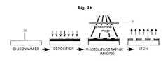
- Photomasksare high precision plates containing microscopic images of electronic circuits. Photomasks are typically made from flat pieces of material that are substantially transparent, such as quartz or glass, with an opaque layer, such as chrome, on one side. Etched in the opaque layer (e.g., chrome) of the mask is a pattern corresponding to a portion of an electronic circuit design.
- a variety of different photomasksincluding for example, aaPSMs, embedded attenuated phase shift masks and binary photomasks (e.g., chrome-on-glass), are used in semiconductor processing to transfer these patterns onto a semiconductor wafer or other type of wafer.
- a photomask 9is interposed between the semiconductor wafer 20 (which includes a layer of photosensitive material) and an optical system 22 .
- Energy generated by an energy source 23commonly referred to as a Stepper, is inhibited from passing through opaque areas of the photomask 9 .
- energy from the Stepperpasses through the substantially transparent portions of the photomask 9 , thereby projecting a diffraction limited, latent image of the pattern on the photomask onto the semiconductor wafer 20 .
- the energy generated by the Steppercauses a reaction in the photosensitive material on the semiconductor wafer such that the solubility of the photosensitive material is changed in areas exposed to the energy.
- the photosensitive material(either exposed or unexposed) is removed from the semiconductor wafer 20 , depending upon the type of photolithographic process being used. For example, where a positive photolithographic process is implemented, the exposed photosensitive material becomes soluble and is removed. By contrast, where a negative photolithographic process is used, the exposed photosensitive material becomes insoluble and the unexposed, soluble photosensitive material is removed. After the appropriate photosensitive material is removed, a pattern corresponding to the photomask 9 appears on the semiconductor wafer 20 . Thereafter, the semiconductor wafer 20 can be used for deposition, etching, and/or ion implantation processes in any combination to form an integrated circuit.
- the devices' sensitivity to the varying exposure tool wavelengthse.g., 248 nm, 193 nm, 157 nm, 13 nm, etc.
- the exposure tool wavelengthse.g., 248 nm, 193 nm, 157 nm, 13 nm, etc.
- the photomaskare exacerbated, thereby increasing the likelihood that defects will manifest in a pattern written on a semiconductor wafer. Accordingly, it has become necessary to develop new methods to minimize the problems associated with these smaller feature sizes.
- PSMsphase shifting masks
- a PSMreduces the diffraction limitation ordinarily associated with a binary COG mask by passing light through substantially transparent areas (e.g., glass or quartz) which have either different thickness and/or different refractive indices than an ordinary binary COG mask.
- substantially transparent arease.g., glass or quartz
- destructive interferenceis created in regions on the target semiconductor wafer that are designed to see no exposure.
- the overall printability of an imageis vastly improved such that the minimum width of a pattern resolved by using a PSM is approximately half the width of a pattern resolved in using an ordinary binary COG mask.
- FIGS. 2 a-billustrate an example of a conventional aaPSM 10 .
- An aaPSMis typically comprised of a layer of opaque material and a substantially transparent substrate which is etched on one side of the opaque features, while not etched on the other side (i.e., etching of the transparent substrate occurs in alternating locations in the substantially transparent substrate).
- the aaPSM 10includes a substantially transparent layer (e.g., quartz) and an opaque layer (e.g., chrome). The opaque layer is etched to form opaque regions 15 and alternating substantially transparent regions 13 , as shown in FIG.
- the substantially transparent regions 13are further etched such that the aaPSM 10 has recesses 14 in the substantially transparent layer.
- the aaPSM 10has substantially transparent regions 13 (which are un-etched) that alternate with etched recesses 14 between each opaque region 15 , as shown in FIGS. 2 a-b .
- the effect of this structure when placed in a Stepperis to create light intensity of alternating polarity and 180° out of phase, as shown in FIG. 2 c .
- This alternating polarityforces energy transmitted from the Stepper to go to zero, in theory, at opaque regions 15 while maintaining the same transmission of light at the alternating transparent regions 13 and recesses 14 . As a result, refraction is reduced through this region.
- d⁇ / 2( n ⁇ 1) where d is film thickness, n is refractive index at exposure wavelength, ⁇ is exposure wavelength.
- the aaPSM of FIG. 2 bhas certain limitations which often preclude the possibility of transferring an accurate image from the aaPSM to a semiconductor wafer.
- the intensity of light transmitted through recess 14will often be less than the intensity of light transmitted through the unetched portions 13 . More particularly, referring to FIG. 2 e , the light intensity is shown for each transmissive region of the aaPSM of FIGS. 2 a and 2 b .
- Length Arepresents the critical dimensions of recess 14
- Length Brepresents the critical dimensions of the unetched portion 13 of the substantially transparent layer. As can be seen, the critical dimensions of these features are asymmetrical (Length B ⁇ Length A).
- the intensity of light transmitted through the unetched portion 13 of the substantially transparent layeris greater than the intensity of light transmitted through the recess 14 .
- This imbalance of light intensity transmitted through these featuresoften make it difficult, if not impossible, to write an accurate image on the a semiconductor wafer using the aaPSM shown in FIG. 2 b.
- Anisotropic featuresare typically formed by using a plasma reactor.
- a fluorocarbon or hydrofluorocarbon etching gasand apply a radio frequency (“RF”) bias to the pedestal supporting the photomask.
- the RF biascreates a direct current (“DC”) bias in the plasma adjacent to the mask.
- the DC biasaccelerates the ions towards the mask and the resulting etch is highly anisotropic with nearly vertical sidewalls.
- wet etching techniqueshave been used to undercut features in the phase shift mask, as shown in FIG. 3 b.
- anisotropic featuresproduce a waveguide effect during wafer printing which induces an aerial image intensity imbalance through focus on the wafer, as shown in FIGS. 3 a - 3 h .
- aerial image intensity imbalance caused by aaPSM quartz features having sidewalls that have been anisotropically etchedcan result in a relative difference of exposure intensity at the wafer plane if the stepper is not in perfect focus.
- the aerial image intensity of the energy transmitted through the aaPSM of FIG. 3 ais approximately 2.8 a.u. for shallow etched features and 2.2 a.u.
- a known method for reducing aerial image intensity imbalanceis to create isotropic trenches in conventional aaPSMs by utilizing: a dry plasma etching step to form an anisotropic trench; and thereafter, a wet hydrofluoric acid (HF) dip, as described in U.S. Patent Application Publication No. 2001/0044056 A1 to isotropically etch the anisotropic trench.
- a dry plasma etching stepto form an anisotropic trench
- a wet hydrofluoric acid (HF) dipas described in U.S. Patent Application Publication No. 2001/0044056 A1 to isotropically etch the anisotropic trench.
- HFwet hydrofluoric acid
- HFis known to be a very toxic and corrosive chemical which is hazardous to handle in a production environment.
- any alternative method that can achieve the same results without resorting to the use of this hazardous materialis preferred.
- HFrequires separate processing equipment, and thus, makes the overall manufacture of photomasks more expensive and time consuming.
- HFis hazardous to the environment, it is necessary to dispose of it in a proper and lawful manner, which can also be costly and burdensome.
- wet etch processis purely isotropic in nature and cannot be tuned to prevent excessive undercut and chrome liftoff. Excessive undercut and chrome liftoff is disadvantageous because it can cause defects. Thus, any process which can limit the need for undercutting chrome is preferred, especially where smaller feature sizes are used.
- An additional concern with respect to wet chemistryis the loading effects of dense to isolated patterned areas. In this regard, an isolated area's etch rates are effected by chemical dilution due to the extreme exposed areas, thereby making it difficult to control the etch time. Thus, wet etching techniques often result in excessive undercut in such exposed areas. Therefore, what is needed is an improved method for manufacturing aaPSMs without an aerial intensity imbalance which avoids using hazardous materials and is tunable to avoid excessive undercut and chrome liftoff and can minimize loading effects.
- aaPSMhaving an intermediate film which balances the aerial intensity between two alternating recesses of different depths.
- the present inventionrelates to a blank photomask comprising: a photosensitive resist material layer; an opaque layer underlying the photosensitive resist material layer; a partially absorbing film layer underlying the opaque layer; and a substantially transparent substrate underlying the partially absorbing film layer.
- the partially absorbing film layercomprises a thickness which substantially balances an aerial image intensity of light transmitted through patterned regions when the blank photomask has been processed into an aaPSM.
- the patterned regionscomprises at least one opening exposing the partially absorbing film layer and at least one light transmitting opening in which the partially absorbing film layer has been removed.
- the present inventionis also directed to a method for creating an aaPSM from the blank photomask described above and comprises the step of providing a blank photomask comprising a photosensitive resist material layer, an opaque layer underlying the photosensitive resist material layer, a partially absorbing film layer underlying the opaque layer, and a substantially transparent substrate underlying the partially absorbing film layer.
- the methodfurther comprises the steps of forming in the blank photomask at least one opening which partially absorbs light, wherein the light absorbing opening exposes the partially absorbing film layer and forming at least one light transmitting opening in the blank photomask.
- the light transmitting openingexposes a portion of the substantially transparent substrate, wherein the partially absorbing film layer comprises a thickness which substantially balances an aerial image intensity of light transmitted through the at least one partially absorbing opening with light transmitted through the at least one light transmitting opening.
- the present inventionis directed to an aaPSM comprising: a substantially transparent substrate having at least one light transmitting opening formed therein; a partially absorbing film layer covering portions of the substantially transparent substrate not defined by the at least one light transmitting opening; and a patterned layer of opaque material affixed to the partially absorbing film.
- the patterned layerexposes at least one portion of the underlying partially absorbing film layer, wherein the partially absorbing film layer comprises a thickness which substantially balances an aerial image intensity of light transmitted through the at least one exposed portion of the at least one partially absorbing film layer with light transmitted through the at least one light transmitting opening.
- an aaPSMcomprises a substantially transparent substrate; a partially absorbing film layer having at least one opening formed therein, wherein portions of the substantially transparent substrate underlying the at least one opening in the partially absorbing film layer are exposed; and a patterned layer of opaque material affixed to the partially absorbing film layer.
- the patterned layer of opaque materialhas at least one opening which exposes underlying portions of the partially absorbing film layer, wherein the partially absorbing film layer comprises a thickness which substantially balances an aerial image intensity of light transmitted through the at least one opening in the opaque layer with light transmitted through at least one opening in the partially absorbing film layer.
- the present inventionis directed to a method for manufacturing a semiconductor comprising the steps of: interposing an aaPSM between a semiconductor wafer and an energy source, wherein the an aaPSM comprises a substantially transparent substrate having at least one light transmitting opening formed therein; a partially absorbing film layer covering portions of the substantially transparent substrate not defined by the at least one light transmitting opening; and a patterned layer of opaque material affixed to the partially absorbing film.
- the patterned layer of the aaPSMexposes at least one portion of the underlying partially absorbing film layer, wherein the partially absorbing film layer comprises a thickness which substantially balances an aerial image intensity of light transmitted through the at least one partially absorbing opening with light transmitted through the at least one light transmitting opening.
- the methodfurther comprises the steps of generating energy in the energy source; transmitting the generated energy through light transmitting opening in the substantially transparent substrate and the at least one exposed partially absorbing film layer; and etching an image on the semiconductor wafer corresponding to the light transmitting opening in the substantially transparent substrate and the at least one exposed partially absorbing film layer.
- the present inventionis directed to a method for manufacturing a semiconductor comprising the steps of: interposing an aaPSM between a semiconductor wafer and an energy source, a substantially transparent substrate; a partially absorbing film layer having at least one opening formed therein, wherein portions of the substantially transparent substrate underlying the opening in the partially absorbing film layer are exposed; and a patterned layer of opaque material affixed to the partially absorbing film layer, the patterned layer of opaque material having at least one opening which exposes underlying portions of the partially absorbing film layer, wherein the partially absorbing film layer comprises a thickness which substantially balances an aerial image intensity of light transmitted through the at least one opening in the opaque layer with light transmitted through at least one opening in the partially absorbing film layer.
- This methodfurther comprises the steps of generating energy in the energy source; transmitting the generated energy through the at least one opening in the partially absorbing film layer and the at least one exposed portion of the partially absorbing film layer; and etching an image on the semiconductor wafer corresponding to at least one opening in the partially absorbing film layer and the at least one exposed portion of the partially absorbing film layer.
- FIG. 1 ashows the equipment which can be used to make a semiconductor device from the aaPSM of the present invention
- FIG. 1 bis flow diagram showing an example of the process for making a semiconductor device
- FIG. 2 ashows a top view of a conventional aaPSM
- FIG. 2 bshows a corresponding side view of the conventional aaPSM shown in FIG. 2 a;
- FIG. 2 cshows the corresponding transmission of light through etched and un-etched regions of the substantially transparent layer of the conventional aaPSM of FIGS. 2 a and 2 b;
- FIG. 2 dshows the corresponding regions in a semiconductor wafer onto which the light is transmitted from the aaPSM shown in FIGS. 2 a and 2 b;
- FIG. 2 edemonstrates how the aaPSM of FIGS. 2 a and 2 b experience an imbalanced light intensity when exposed to an energy source
- FIG. 3 ashows a side view of an anistropically etched aaPSM
- FIG. 3 bshows a side view of an aaPSM having anisotropic trenches that have been isotropically undercut using wet etching techniques
- FIG. 3 cshows the aerial image intensity of the aaPSM of FIG. 3 a when the Stepper is in perfect focus
- FIG. 3 dshows the aerial image intensity of the aaPSM of FIG. 3 b when the Stepper is in perfect focus
- FIG. 3 eshows the aerial image intensity of the aaPSM of FIG. 3 a when the Stepper is out of focus
- FIG. 3 fshows the aerial image intensity of the aaPSM of FIG. 3 b when the Stepper is out of focus
- FIG. 3 gis a graph showing the aerial image intensity for deep and shallow etched trenches of the aaPSM of FIG. 3 a at different focus levels;
- FIG. 3 his a graph showing the aerial image intensity for deep and shallow etched trenches of the aaPSM of FIG. 3 b at different focus levels;
- FIG. 4 ashows a cross-sectional view of conventional aaPSM having an anisotropic trench
- FIG. 4 bshows a cross-sectional view of conventional aaPSM having an isotropic trench
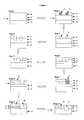
- FIG. 5shows a cross-sectional view of a photomask blank made in accordance with the present invention
- FIG. 6shows a finished aaPSM made in accordance with the present invention using the photomask blank of FIG. 5 ;
- FIG. 7shows one embodiment of the method for manufacturing the aaPSM shown in FIG. 6 ;
- FIG. 8shows another embodiment by which the photomask blank of FIG. 5 is processed into a finished photomask.
- the present inventionis directed to an improved aaPSM and method for making the same. More particularly, the present invention utilizes a partially absorbent, intermediate film in a blank photomask to make an aaPSM which transmits balanced light intensities through each opening in the finished aaPSM. By utilizing a partially absorbent intermediate film in this manner, the step of undercutting the opaque layer of the aaPSM is no longer needed.
- the blank photomask 31preferably includes four layers, but may include additional layers as needed or desired by the photomask maker.
- the blank photomask 31includes a substantially transparent layer 33 , such as quartz.
- the next layeris a film 35 which is made from materials that are capable of both partially absorbing light and partially transmitting light. Since the photomask 31 will ultimately be processed into an aaPSM, the film should be tuned to have an index and thickness such that, when exposed to an energy source, the light transmitted therethrough will be partially absorbed so as to be in balance with light transmitted through the trenches 38 and 40 (described below) formed in the aaPSM.
- the thickness of the film 35should be selected in conjunction with the depth of the alternating recess and trenches of the aaPSM of the present invention so as to ensure that the light transmitted through said alternating recesses and trenches is approximately 180° out of phase.
- the present inventionmay be used in conjunction with a lateral size bias or lateral size adjustment of either the recesses, trenches or opaque region.
- a variety of materialscan be used as the film 35 of the present invention, including, but not limited to, MgF 2 , amorphous-Si, Si 3 N 4 , SiON, CrO, CrON, TiN, TiO, TaO, TaN, MoO, MoN, MoON, and any oxide, nitride, fluoride or oxynitride of any metallic element.
- the next layeris a substantially opaque layer 37 (e.g, chrome) capable of absorbing all (or most) light to which it is exposed.
- the opaque layer 37may additionally include an anti-reflective layer, such as chrome oxide, if desired or needed.
- the next layeris a photosensitive material 39 .
- a pattern defined by an electronic fileis transferred to the blank photomask using conventional lithography tools, including, for example, E-beam and/or laser beam writing tools.
- the laser source which is usedoperates at 365 nm, however, the present invention is not limited to this particular wavelength laser source and will work with a variety of different image sources as discussed herein.
- the blank photomask 31is etched to form an aaPSM 41 having types of transmissive regions: (1) an unetched, film recess 40 covering a corresponding unetched portion of the substantially transparent layer 33 ; and (2) a subtractively etched trench 38 etched in the substantially transparent layer 33 . These transmissive regions alternate between opaque regions on the photomask, as shown in FIG. 6 .
- an opaque regionis defined in the photomask. In one embodiment, this is accomplished by several steps. Referring to FIG. 7 , the blank photomask of FIG. 5 is provided, Step 1 . Predefined areas 32 in the photosensitive resist layer 39 of the blank photomask 31 are exposed to an energy source (e.g., a light source), Step 2 . Thereafter, the exposed photoresist 32 is developed (i.e., removed), thereby forming a recess 34 in the photosensitive resist layer 31 , Step 3 .
- an energy sourcee.g., a light source
- the portions of the opaque layer 37 underlying the recesses 34are removed by conventional etching techniques (e.g., dry etching or chemical etching), Step 4 . Thereafter, the remaining photosensitive resist 39 overlying the undeveloped portions of the opaque layer 37 is removed, thereby exposing portions of the film 35 underlying the removed portions of the opaque layer 37 , Step 5 .
- the un-etched portions of the opaque layer 33serve to block the exposure light during wafer printing, whereas the portions of the opaque layer which have been etched away define the region of the film 35 and substantially transparent layer 33 which allows exposure light from the Stepper to pass through.
- the first processing stage of the method of the present inventionis used to form a modified version of a conventional binary photomask by patterning an opaque layer.
- the exposed areas 36 of the photosensitive resist layer 39are developed (i.e., removed), Step 8 .
- the portions of the film 35 and the corresponding, underlying portions of the substantially transparent layer 33 that are no longer covered by photosensitive resist material 39 (or opaque material 33 )are etched to a specified depth, Step 9 .
- a phase shifted, transmissive vertical trench 43is formed in the substantially transparent layer 35 .
- the remaining photoresist 39is removed, Step 10 .
- the resultis an aaPSM having a vertical trench 38 alternating with unetched recess 40 of the substantially transparent layer that are covered by the film 35 .
- the specified depth and the thickness of film 35are determined so that the light that passes through the unetched recess 40 is approximately 180° out of phase from light that passes through the vertical trench 38 .
- the method for processing the aaPSM of the present inventionis not limited to the particular processing steps. In this regard, the processing method could be modified so long as the same results are achieved. Additionally, it is noted that the aaPSM of the present invention can be modified to be etched to different depths.
- the blank photomask of FIG. 5could be processed to form a modified aaPSM in which the substantially transparent layer does not need to be etched.
- the blank photomask 31could be processed to form a pattern in the mask having alternating trench depths wherein a first trench 51 is formed by simply removing the pre-defined portion of the opaque layer 37 , thereby exposing the underlying partially absorbing film 51 .
- a second trench 53is formed by removing a second predefined portion of the opaque layer 37 and additionally removing the underlying portion of the partially absorbing film 35 which corresponds to the second predefined portion of the opaque layer 37 .
- additionally trenchesmay need to be formed depending on the overall design of the photomask.
- the partially absorbing film 35should be of a sufficient thickness such that the phase delay of light transmitted through the first trench 51 and the second trench 53 approximately 180° out of phase and otherwise substantially equal. Depending upon the application, it may be desirable to use a thicker film and a shallower trench, or vice versa. The film thickness could be calculated through trial and error, through photomask modeling techniques or other known techniques. An additional advantage of this embodiment is that the trenches and recesses will have a natural etch stop for these manufacturing processes.
- the present inventionis not limited to the precise processing steps described herein.
- the aaPSM of the present inventionmay be made with fewer or more processing steps, depending upon the equipment used and needs of the photomask maker.
- the method of the present inventionmay also, for example, form all the unetched regions 40 in a series of processing steps, and form the etched regions 38 in a second series of processing steps.
Landscapes
- Physics & Mathematics (AREA)
- General Physics & Mathematics (AREA)
- Preparing Plates And Mask In Photomechanical Process (AREA)
- Exposure And Positioning Against Photoresist Photosensitive Materials (AREA)
Abstract
Description
d=λ/2(n−1)
where d is film thickness, n is refractive index at exposure wavelength, λ is exposure wavelength. Thus, it is possible to etch smaller features in a semiconductor wafer and use shorter exposure wavelengths. Since the photoresist layer on the semiconductor wafer (
Claims (26)
Priority Applications (4)
| Application Number | Priority Date | Filing Date | Title |
|---|---|---|---|
| US10/391,001US6933084B2 (en) | 2003-03-18 | 2003-03-18 | Alternating aperture phase shift photomask having light absorption layer |
| PCT/US2004/005606WO2004083960A2 (en) | 2003-03-18 | 2004-02-26 | Alternating aperture phase shift photomask having light absorption layer |
| TW093106850ATWI287692B (en) | 2003-03-18 | 2004-03-15 | Alternating aperture phase shift photomask and fabricating method thereof and method for manufacturing a semiconductor using the alternating aperture phase shift photomask |
| US11/024,268US7344824B2 (en) | 2003-03-18 | 2004-12-28 | Alternating aperture phase shift photomask having light absorption layer |
Applications Claiming Priority (1)
| Application Number | Priority Date | Filing Date | Title |
|---|---|---|---|
| US10/391,001US6933084B2 (en) | 2003-03-18 | 2003-03-18 | Alternating aperture phase shift photomask having light absorption layer |
Related Child Applications (1)
| Application Number | Title | Priority Date | Filing Date |
|---|---|---|---|
| US11/024,268DivisionUS7344824B2 (en) | 2003-03-18 | 2004-12-28 | Alternating aperture phase shift photomask having light absorption layer |
Publications (2)
| Publication Number | Publication Date |
|---|---|
| US20040185348A1 US20040185348A1 (en) | 2004-09-23 |
| US6933084B2true US6933084B2 (en) | 2005-08-23 |
Family
ID=32987615
Family Applications (2)
| Application Number | Title | Priority Date | Filing Date |
|---|---|---|---|
| US10/391,001Expired - LifetimeUS6933084B2 (en) | 2003-03-18 | 2003-03-18 | Alternating aperture phase shift photomask having light absorption layer |
| US11/024,268Expired - LifetimeUS7344824B2 (en) | 2003-03-18 | 2004-12-28 | Alternating aperture phase shift photomask having light absorption layer |
Family Applications After (1)
| Application Number | Title | Priority Date | Filing Date |
|---|---|---|---|
| US11/024,268Expired - LifetimeUS7344824B2 (en) | 2003-03-18 | 2004-12-28 | Alternating aperture phase shift photomask having light absorption layer |
Country Status (3)
| Country | Link |
|---|---|
| US (2) | US6933084B2 (en) |
| TW (1) | TWI287692B (en) |
| WO (1) | WO2004083960A2 (en) |
Families Citing this family (9)
| Publication number | Priority date | Publication date | Assignee | Title |
|---|---|---|---|---|
| JP2008515006A (en)* | 2004-09-27 | 2008-05-08 | トッパン、フォウタマスクス、インク | Phase shift mask providing balanced light intensity through different phase shift apertures and method of forming such a phase shift mask |
| KR100629359B1 (en)* | 2005-08-09 | 2006-10-02 | 삼성전자주식회사 | Methods for manufacturing a semiconductor device using a photosensitive polyimide film and semiconductor devices manufactured thereby |
| JP4607151B2 (en)* | 2006-07-06 | 2011-01-05 | エーエスエムエル マスクツールズ ビー.ブイ. | Improved CPL mask and method and program product for generating the same |
| US8003537B2 (en)* | 2006-07-18 | 2011-08-23 | Imec | Method for the production of planar structures |
| US8318536B2 (en)* | 2007-12-31 | 2012-11-27 | Intel Corporation | Utilizing aperture with phase shift feature in forming microvias |
| US20110159411A1 (en)* | 2009-12-30 | 2011-06-30 | Bennett Olson | Phase-shift photomask and patterning method |
| US9436092B2 (en)* | 2012-03-30 | 2016-09-06 | Newport Fab, Llc | Semiconductor fabrication utilizing grating and trim masks |
| KR102246872B1 (en) | 2014-07-29 | 2021-04-30 | 삼성전자 주식회사 | Photomask including focus metrology mark, substrate target including focus monitor pattern, metrology method for lithography process, and method of manufacturing integrated circuit device |
| KR102502202B1 (en)* | 2015-06-29 | 2023-02-21 | 삼성디스플레이 주식회사 | Light emitting display device and fabricating of the same |
Citations (29)
| Publication number | Priority date | Publication date | Assignee | Title |
|---|---|---|---|---|
| US4178403A (en) | 1977-08-04 | 1979-12-11 | Konishiroku Photo Industry Co., Ltd. | Mask blank and mask |
| US4556608A (en) | 1980-10-09 | 1985-12-03 | Dai Nippon Insatsu Kabushiki Kaisha | Photomask blank and photomask |
| US4720442A (en) | 1985-05-28 | 1988-01-19 | Asahi Glass Company Ltd. | Photomask blank and photomask |
| JPH0239153A (en) | 1988-07-29 | 1990-02-08 | Toppan Printing Co Ltd | Photomask blank and photomask |
| JPH07104457A (en) | 1993-08-13 | 1995-04-21 | Toshiba Corp | Exposure mask, manufacturing method and manufacturing apparatus therefor |
| US5451543A (en) | 1994-04-25 | 1995-09-19 | Motorola, Inc. | Straight sidewall profile contact opening to underlying interconnect and method for making the same |
| US5460908A (en) | 1991-08-02 | 1995-10-24 | Micron Technology, Inc. | Phase shifting retical fabrication method |
| US5472811A (en) | 1993-01-21 | 1995-12-05 | Sematech, Inc. | Phase shifting mask structure with multilayer optical coating for improved transmission |
| US5477058A (en) | 1994-11-09 | 1995-12-19 | Kabushiki Kaisha Toshiba | Attenuated phase-shifting mask with opaque reticle alignment marks |
| US5482799A (en) | 1993-10-08 | 1996-01-09 | Mitsubishi Denki Kabushiki Kaisha | Phase shift mask and manufacturing method thereof |
| JPH0876353A (en) | 1994-09-08 | 1996-03-22 | Nec Corp | Production of phase shift mask |
| US5547787A (en) | 1992-04-22 | 1996-08-20 | Kabushiki Kaisha Toshiba | Exposure mask, exposure mask substrate, method for fabricating the same, and method for forming pattern based on exposure mask |
| US5578402A (en) | 1990-06-21 | 1996-11-26 | Matsushita Electronics Corporation | Photomask used by photolithography and a process of producing same |
| US5693568A (en) | 1995-12-14 | 1997-12-02 | Advanced Micro Devices, Inc. | Reverse damascene via structures |
| US5725973A (en) | 1994-02-07 | 1998-03-10 | Samsung Electronic Co., Ltd. | Photo mask and method for manufacturing same |
| US5756396A (en) | 1996-05-06 | 1998-05-26 | Taiwan Semiconductor Manufacturing Company Ltd | Method of making a multi-layer wiring structure having conductive sidewall etch stoppers and a stacked plug interconnect |
| US5932377A (en)* | 1998-02-24 | 1999-08-03 | International Business Machines Corporation | Exact transmission balanced alternating phase-shifting mask for photolithography |
| US5935733A (en) | 1996-04-05 | 1999-08-10 | Intel Corporation | Photolithography mask and method of fabrication |
| US5939227A (en) | 1998-03-09 | 1999-08-17 | Rochester Institute Of Technology | Multi-layered attenuated phase shift mask and a method for making the mask |
| US5955222A (en) | 1996-12-03 | 1999-09-21 | International Business Machines Corporation | Method of making a rim-type phase-shift mask and mask manufactured thereby |
| US6187480B1 (en) | 1998-04-03 | 2001-02-13 | United Microelectronics Corp. | Alternating phase-shifting mask |
| JP2001174973A (en) | 1999-12-15 | 2001-06-29 | Dainippon Printing Co Ltd | Halftone phase shift photomask and blank for halftone phase shift photomask |
| US6291113B1 (en)* | 1999-10-21 | 2001-09-18 | Advanced Micro Devices, Inc. | Sidelobe suppressing phase shift mask and method |
| US20010044056A1 (en) | 2000-05-17 | 2001-11-22 | Haruo Kokubo | Phase-shift photomask manufacturing method and phase-shift photomask |
| US6335130B1 (en) | 2000-05-01 | 2002-01-01 | Asml Masktools Netherlands B.V. | System and method of providing optical proximity correction for features using phase-shifted halftone transparent/semi-transparent features |
| US6355557B2 (en) | 1998-07-22 | 2002-03-12 | Applied Materials, Inc. | Oxide plasma etching process with a controlled wineglass shape |
| US6492069B1 (en)* | 2000-03-10 | 2002-12-10 | Worldwide Semiconductor Manufacturing Corp. | Method for forming an attenuated phase-shifting mask |
| US6743553B2 (en) | 2000-12-26 | 2004-06-01 | Hoya Corporation | Halftone phase shift mask and mask blank |
| US6780548B1 (en) | 2001-01-11 | 2004-08-24 | Dupont Photomasks, Inc. | Alternating aperture phase shifting photomask with improved transmission balancing |
- 2003
- 2003-03-18USUS10/391,001patent/US6933084B2/ennot_activeExpired - Lifetime
- 2004
- 2004-02-26WOPCT/US2004/005606patent/WO2004083960A2/enactiveApplication Filing
- 2004-03-15TWTW093106850Apatent/TWI287692B/ennot_activeIP Right Cessation
- 2004-12-28USUS11/024,268patent/US7344824B2/ennot_activeExpired - Lifetime
Patent Citations (29)
| Publication number | Priority date | Publication date | Assignee | Title |
|---|---|---|---|---|
| US4178403A (en) | 1977-08-04 | 1979-12-11 | Konishiroku Photo Industry Co., Ltd. | Mask blank and mask |
| US4556608A (en) | 1980-10-09 | 1985-12-03 | Dai Nippon Insatsu Kabushiki Kaisha | Photomask blank and photomask |
| US4720442A (en) | 1985-05-28 | 1988-01-19 | Asahi Glass Company Ltd. | Photomask blank and photomask |
| JPH0239153A (en) | 1988-07-29 | 1990-02-08 | Toppan Printing Co Ltd | Photomask blank and photomask |
| US5578402A (en) | 1990-06-21 | 1996-11-26 | Matsushita Electronics Corporation | Photomask used by photolithography and a process of producing same |
| US5460908A (en) | 1991-08-02 | 1995-10-24 | Micron Technology, Inc. | Phase shifting retical fabrication method |
| US5547787A (en) | 1992-04-22 | 1996-08-20 | Kabushiki Kaisha Toshiba | Exposure mask, exposure mask substrate, method for fabricating the same, and method for forming pattern based on exposure mask |
| US5472811A (en) | 1993-01-21 | 1995-12-05 | Sematech, Inc. | Phase shifting mask structure with multilayer optical coating for improved transmission |
| JPH07104457A (en) | 1993-08-13 | 1995-04-21 | Toshiba Corp | Exposure mask, manufacturing method and manufacturing apparatus therefor |
| US5482799A (en) | 1993-10-08 | 1996-01-09 | Mitsubishi Denki Kabushiki Kaisha | Phase shift mask and manufacturing method thereof |
| US5725973A (en) | 1994-02-07 | 1998-03-10 | Samsung Electronic Co., Ltd. | Photo mask and method for manufacturing same |
| US5451543A (en) | 1994-04-25 | 1995-09-19 | Motorola, Inc. | Straight sidewall profile contact opening to underlying interconnect and method for making the same |
| JPH0876353A (en) | 1994-09-08 | 1996-03-22 | Nec Corp | Production of phase shift mask |
| US5477058A (en) | 1994-11-09 | 1995-12-19 | Kabushiki Kaisha Toshiba | Attenuated phase-shifting mask with opaque reticle alignment marks |
| US5693568A (en) | 1995-12-14 | 1997-12-02 | Advanced Micro Devices, Inc. | Reverse damascene via structures |
| US5935733A (en) | 1996-04-05 | 1999-08-10 | Intel Corporation | Photolithography mask and method of fabrication |
| US5756396A (en) | 1996-05-06 | 1998-05-26 | Taiwan Semiconductor Manufacturing Company Ltd | Method of making a multi-layer wiring structure having conductive sidewall etch stoppers and a stacked plug interconnect |
| US5955222A (en) | 1996-12-03 | 1999-09-21 | International Business Machines Corporation | Method of making a rim-type phase-shift mask and mask manufactured thereby |
| US5932377A (en)* | 1998-02-24 | 1999-08-03 | International Business Machines Corporation | Exact transmission balanced alternating phase-shifting mask for photolithography |
| US5939227A (en) | 1998-03-09 | 1999-08-17 | Rochester Institute Of Technology | Multi-layered attenuated phase shift mask and a method for making the mask |
| US6187480B1 (en) | 1998-04-03 | 2001-02-13 | United Microelectronics Corp. | Alternating phase-shifting mask |
| US6355557B2 (en) | 1998-07-22 | 2002-03-12 | Applied Materials, Inc. | Oxide plasma etching process with a controlled wineglass shape |
| US6291113B1 (en)* | 1999-10-21 | 2001-09-18 | Advanced Micro Devices, Inc. | Sidelobe suppressing phase shift mask and method |
| JP2001174973A (en) | 1999-12-15 | 2001-06-29 | Dainippon Printing Co Ltd | Halftone phase shift photomask and blank for halftone phase shift photomask |
| US6492069B1 (en)* | 2000-03-10 | 2002-12-10 | Worldwide Semiconductor Manufacturing Corp. | Method for forming an attenuated phase-shifting mask |
| US6335130B1 (en) | 2000-05-01 | 2002-01-01 | Asml Masktools Netherlands B.V. | System and method of providing optical proximity correction for features using phase-shifted halftone transparent/semi-transparent features |
| US20010044056A1 (en) | 2000-05-17 | 2001-11-22 | Haruo Kokubo | Phase-shift photomask manufacturing method and phase-shift photomask |
| US6743553B2 (en) | 2000-12-26 | 2004-06-01 | Hoya Corporation | Halftone phase shift mask and mask blank |
| US6780548B1 (en) | 2001-01-11 | 2004-08-24 | Dupont Photomasks, Inc. | Alternating aperture phase shifting photomask with improved transmission balancing |
Non-Patent Citations (9)
| Title |
|---|
| Armin Semmler, L. Mader, A. Elsner, R. Koehle, U. Griesinger, C. Noelscher, "Application of 3D EMF Simulation for Development and Optimization of Alternating Phase Shifting Masks", Optical Microlithography XIV, Proceedings of SPIE, 2001, P. 356-367, vol. 4346 (Christopher J. Progler, ed.). |
| Canon Presentation, "Canon's IDEAL: Innovative Double Exposure by Advanced Lithography," BACUS News, SPIE, Apr. 2001, vol. 17, Issue 4, p. 1-7. |
| K.D. Lucas, C.M. Yuan, and A.J. Stroljwas, "A rigorous and practical vector model for phase shigting masks in optical lithography", Proc. SPIE 1674, 252-263 (1992). |
| M.D. Levenson, N.S. Viswanathan, and R.A. Simpson, "Improving Resolution with a Phase-Shifting Mask", IEEE Trans. Elect. Dev. ED-29, 1828-1836 (1982). |
| Peng, Song, "Through-Focus Image Balancing of Alternating Phase Shifting Masks", SPIE vol. 3873, p. 328-336 (1999). |
| R.L. Kosetelak, C. Pierrat, J.G. Garofalo, and S. Vaidya, "Exposure characteristics of alternate aperture phase-shifting masks fabricated using a subtractive process", J. Vac. Sci. Tech. B0, 3055-3061 (1992). |
| T. Ebihara, T. Oga, P.D. Rhyins, M. Sweis, P.M. Martin, "150-nm dense/isolated contact hole study with Canon IDEAL technique", SPIE Proceeding 4562-119. |
| T. Terasawa, N. Hasegawa, A. Imai and S. Okazaki, "Analysis of Nonplanar Topography Effects of Phase Shift Masks on Imaging Characteristics", Japanese J. Appl. Phys. 34, 6578-6583 (1995). |
| T. Teresawa, N. Hasegawa, T. Tanaka, S. Katagiri, and T. Kurosaki, "Improved Resolution of an i-line stepper using a phase-shift mask", J.Vac. Sci. Tech. B8, 1300-1308, (1990). |
Also Published As
| Publication number | Publication date |
|---|---|
| US20040185348A1 (en) | 2004-09-23 |
| WO2004083960A3 (en) | 2005-02-03 |
| TW200506505A (en) | 2005-02-16 |
| TWI287692B (en) | 2007-10-01 |
| WO2004083960A2 (en) | 2004-09-30 |
| US7344824B2 (en) | 2008-03-18 |
| US20050170288A1 (en) | 2005-08-04 |
Similar Documents
| Publication | Publication Date | Title |
|---|---|---|
| US5932377A (en) | Exact transmission balanced alternating phase-shifting mask for photolithography | |
| US6458495B1 (en) | Transmission and phase balance for phase-shifting mask | |
| KR20000057061A (en) | Photomask and manufacturing method thereof, and exposure method using the photomask | |
| US7312004B2 (en) | Embedded attenuated phase shift mask with tunable transmission | |
| US6933084B2 (en) | Alternating aperture phase shift photomask having light absorption layer | |
| US5495959A (en) | Method of making substractive rim phase shifting masks | |
| US7049034B2 (en) | Photomask having an internal substantially transparent etch stop layer | |
| US5853921A (en) | Methods of fabricating phase shift masks by controlling exposure doses | |
| US20040086787A1 (en) | Alternating aperture phase shift photomask having plasma etched isotropic quartz features | |
| US6093507A (en) | Simplified process for fabricating levinson and chromeless type phase shifting masks | |
| US20050026053A1 (en) | Photomask having an internal substantially transparent etch stop layer | |
| EP0553543B1 (en) | Phase shift mask and method for forming resist pattern using said mask | |
| JP2005257962A (en) | Phase shift mask and method for manufacturing phase shift mask | |
| US8589826B2 (en) | Photomask constructions having liners of specified compositions along sidewalls of multi-layered structures | |
| JPH08123008A (en) | Phase shift mask and manufacturing method thereof | |
| WO2005103820A1 (en) | Levenson type phase shift mask and production method therefor | |
| JP2010191009A (en) | Photomask and method for manufacturing the same | |
| JPH05289305A (en) | Phase shift photomask | |
| JPH08106151A (en) | Phase shift mask and its production | |
| US8158015B2 (en) | Fitting methodology of etching times determination for a mask to provide critical dimension and phase control | |
| JP6315033B2 (en) | Photo mask | |
| US6720114B1 (en) | Method of forming an alternating phase shift circuitry fabrication mask, method of forming a circuitry fabrication mask having a subtractive alternating phase shift region, and alternating phase shift mask | |
| JP4582574B2 (en) | Phase shift mask and manufacturing method thereof | |
| JP3241793B2 (en) | Phase shift photomask | |
| JP6035884B2 (en) | Photomask manufacturing method |
Legal Events
| Date | Code | Title | Description |
|---|---|---|---|
| AS | Assignment | Owner name:PHOTRONICS, INC., FLORIDA Free format text:ASSIGNMENT OF ASSIGNORS INTEREST;ASSIGNOR:PROGLER, CHRISTOPHER J.;REEL/FRAME:013881/0076 Effective date:20030318 | |
| AS | Assignment | Owner name:PHOTRONICS, INC., A CORP. OF CONNECTICUT, CONNECTI Free format text:CORRECTIVE DOCUMENT TO CORRECT ASSIGNEE'S ADDRESS AND STATE OF INCORPORATION ON ORIGINAL ASSIGNMENT, RECORDED 03/18/2003 AT REEL 013881 FRAME 0076.;ASSIGNOR:PROGLER, CHRISTOPHER J.;REEL/FRAME:016991/0756 Effective date:20030318 | |
| STCF | Information on status: patent grant | Free format text:PATENTED CASE | |
| AS | Assignment | Owner name:JPMORGAN CHASE BANK, NATIONAL ASSOCIATION, ILLINOI Free format text:SECURITY AGREEMENT;ASSIGNOR:PHOTRONICS, INC.;REEL/FRAME:021976/0635 Effective date:20081212 Owner name:JPMORGAN CHASE BANK, NATIONAL ASSOCIATION,ILLINOIS Free format text:SECURITY AGREEMENT;ASSIGNOR:PHOTRONICS, INC.;REEL/FRAME:021976/0635 Effective date:20081212 | |
| AS | Assignment | Owner name:JPMORGAN CHASE BANK, NATIONAL ASSOCIATION, ILLINOI Free format text:SECURITY AGREEMENT;ASSIGNOR:PHOTRONICS, INC.;REEL/FRAME:022012/0009 Effective date:20081212 Owner name:JPMORGAN CHASE BANK, NATIONAL ASSOCIATION,ILLINOIS Free format text:SECURITY AGREEMENT;ASSIGNOR:PHOTRONICS, INC.;REEL/FRAME:022012/0009 Effective date:20081212 | |
| FPAY | Fee payment | Year of fee payment:4 | |
| AS | Assignment | Owner name:JPMORGAN CHASE BANK, N.A., AS COLLATERAL AGENT,ILL Free format text:SECURITY AGREEMENT;ASSIGNOR:PHOTRONICS, INC.;REEL/FRAME:023928/0612 Effective date:20100212 Owner name:JPMORGAN CHASE BANK, N.A., AS COLLATERAL AGENT, IL Free format text:SECURITY AGREEMENT;ASSIGNOR:PHOTRONICS, INC.;REEL/FRAME:023928/0612 Effective date:20100212 | |
| FPAY | Fee payment | Year of fee payment:8 | |
| FPAY | Fee payment | Year of fee payment:12 | |
| AS | Assignment | Owner name:JPMORGAN CHASE BANK, N.A., AS COLLATERAL AGENT, ILLINOIS Free format text:SECURITY INTEREST;ASSIGNOR:PHOTRONICS, INC.;REEL/FRAME:047002/0633 Effective date:20180927 Owner name:JPMORGAN CHASE BANK, N.A., AS COLLATERAL AGENT, IL Free format text:SECURITY INTEREST;ASSIGNOR:PHOTRONICS, INC.;REEL/FRAME:047002/0633 Effective date:20180927 |