US6930885B2 - Densely packed electronic assemblage with heat removing element - Google Patents
Densely packed electronic assemblage with heat removing elementDownload PDFInfo
- Publication number
- US6930885B2 US6930885B2US10/328,312US32831202AUS6930885B2US 6930885 B2US6930885 B2US 6930885B2US 32831202 AUS32831202 AUS 32831202AUS 6930885 B2US6930885 B2US 6930885B2
- Authority
- US
- United States
- Prior art keywords
- heat
- generating component
- heat generating
- densely packed
- thermally conductive
- Prior art date
- Legal status (The legal status is an assumption and is not a legal conclusion. Google has not performed a legal analysis and makes no representation as to the accuracy of the status listed.)
- Expired - Lifetime, expires
Links
Images


Classifications
- H—ELECTRICITY
- H05—ELECTRIC TECHNIQUES NOT OTHERWISE PROVIDED FOR
- H05K—PRINTED CIRCUITS; CASINGS OR CONSTRUCTIONAL DETAILS OF ELECTRIC APPARATUS; MANUFACTURE OF ASSEMBLAGES OF ELECTRICAL COMPONENTS
- H05K1/00—Printed circuits
- H05K1/02—Details
- H05K1/0201—Thermal arrangements, e.g. for cooling, heating or preventing overheating
- H05K1/0203—Cooling of mounted components
- H05K1/0204—Cooling of mounted components using means for thermal conduction connection in the thickness direction of the substrate
- H05K1/0206—Cooling of mounted components using means for thermal conduction connection in the thickness direction of the substrate by printed thermal vias
- H—ELECTRICITY
- H01—ELECTRIC ELEMENTS
- H01L—SEMICONDUCTOR DEVICES NOT COVERED BY CLASS H10
- H01L23/00—Details of semiconductor or other solid state devices
- H01L23/34—Arrangements for cooling, heating, ventilating or temperature compensation ; Temperature sensing arrangements
- H01L23/36—Selection of materials, or shaping, to facilitate cooling or heating, e.g. heatsinks
- H01L23/367—Cooling facilitated by shape of device
- H01L23/3677—Wire-like or pin-like cooling fins or heat sinks
- H—ELECTRICITY
- H01—ELECTRIC ELEMENTS
- H01L—SEMICONDUCTOR DEVICES NOT COVERED BY CLASS H10
- H01L2924/00—Indexing scheme for arrangements or methods for connecting or disconnecting semiconductor or solid-state bodies as covered by H01L24/00
- H01L2924/0001—Technical content checked by a classifier
- H01L2924/0002—Not covered by any one of groups H01L24/00, H01L24/00 and H01L2224/00
- H—ELECTRICITY
- H05—ELECTRIC TECHNIQUES NOT OTHERWISE PROVIDED FOR
- H05K—PRINTED CIRCUITS; CASINGS OR CONSTRUCTIONAL DETAILS OF ELECTRIC APPARATUS; MANUFACTURE OF ASSEMBLAGES OF ELECTRICAL COMPONENTS
- H05K2201/00—Indexing scheme relating to printed circuits covered by H05K1/00
- H05K2201/09—Shape and layout
- H05K2201/09209—Shape and layout details of conductors
- H05K2201/09654—Shape and layout details of conductors covering at least two types of conductors provided for in H05K2201/09218 - H05K2201/095
- H05K2201/09781—Dummy conductors, i.e. not used for normal transport of current; Dummy electrodes of components
- H—ELECTRICITY
- H05—ELECTRIC TECHNIQUES NOT OTHERWISE PROVIDED FOR
- H05K—PRINTED CIRCUITS; CASINGS OR CONSTRUCTIONAL DETAILS OF ELECTRIC APPARATUS; MANUFACTURE OF ASSEMBLAGES OF ELECTRICAL COMPONENTS
- H05K3/00—Apparatus or processes for manufacturing printed circuits
- H05K3/40—Forming printed elements for providing electric connections to or between printed circuits
- H05K3/42—Plated through-holes or plated via connections
- H05K3/429—Plated through-holes specially for multilayer circuits, e.g. having connections to inner circuit layers
Definitions
- the inventionrelates generally to the field of broad electronic technology (BET), and in particular to thermal management of highly dense circuit boards. More specifically, the invention relates to a method of reducing the heat of heat-generating electronic components during service.
- BETbroad electronic technology
- an electronic assemblagehas a heat-removing element associated with a heat-generating element for reducing the junction temperature of the heat-generating component by means of a plurality of thermal vias.
- a densely packed electronic assemblagecomprises a substrate medium for supporting at least one heat generating component thereon.
- the heat-generating componenthas a characteristic junction temperature T j .
- a first heat removing elementis thermally associated with the heat generating component and reduces the junction temperature T j of the heat generating component.
- the heat-removing elementis spaced apart from the heat-generating component so as to produce an open space nearest to the heat-generating component for accommodating high density electrical layouts.
- a heat sink in fluid communications with the first heat removing elementabsorbs heat from the heat generating component and thereby reduces its junction temperature T j to a temperature T 1 , wherein T 1 is less than T j .
- the present inventionhas numerous advantages over prior art developments. More particularly, the densely packed electronic assemblage of the invention operates at lower temperatures and is, therefore, more reliable. Further, the electronic assemblage can allocate space in proximity to the heat-generating element for specific electrical traces essential for the design layout. Furthermore, the electronic assemblage of the invention may contain a larger number of standard and thinner width size components.
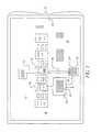
- FIG. 1is a plane view of a portion of an electronic assemblage in accordance with the invention
- FIG. 2is a cross-sectional view of an electronic assemblage in accordance with the invention.
- FIG. 3is an enlarged partial sectional view of an electronic assemblage of the invention.
- FIG. 4is a cross-sectional view of a multi-layer circuit board containing a first and a fourth heat removing element.
- electronic assemblage 10 of the inventionhas a substrate medium 12 , or typically a circuit board, having mounted thereon at least one heat generating components 14 , 30 .
- Heat generating component 14may include any number of components that generate heat during operations or under load, such as resistors, diodes, transistors, processors, etc. Skilled artisans will appreciate that each heat generating component 14 has a characteristic junction temperature T j , i.e., the die temperature during operation. During operations, as the heat generating component 14 approaches its maximum junction temperature, the prospect for component failure, and thus reliability problems becomes eminent.
- each heat generating component 14 in the electronic assemblage 10be associated with a novel and unobvious at least first heat removing element 16 for reducing the junction temperature T j of the heat generating component 14 to a temperature T 1 , where T 1 is considerably less than T j .
- First heat removing element 16comprising a plurality of patterned thermal vias 24 , forms a conduction path for carrying heat away from heat generating component 14 , as described further below.
- a heat sink 20is preferably associated with first heat removing element 16 . Heat sink 20 absorbs and transfers heat transported between the conduction path and the heat generating component 14 . In this way, excess heat from overheated heat generating component 14 is continually directed away from the electronic assemblage 10 , thereby preserving the reliability and performance of the electronic assemblage 10 and any heat sensitive component therein.
- substrate medium 12 of electronic assemblage 10may be a multi-layer circuit board, e.g., a 14-layer polyimide circuit board that uses 1 oz. copper on the inner layers 44 and 2 oz. copper on the outermost layers 46 , 48 .
- Skilled artisanswill appreciate that any circuit board material is contemplated by the invention, since the primary heat transfer mechanism is thermal conduction via the plurality of thermal vias 24 of heat removal element 16 .
- substrate medium 12uses copper as the base trace 50 with a plating of nickel gold (NiAu).
- NiAunickel gold
- Current industry standards for platinginclude palladium (Pd), nickel gold (NiAu), Immersion Tin, Immersion silver, and hot air solder level (HASL).
- Pdpalladium
- NiAunickel gold
- HSLhot air solder level
- the specific circuit board material used in the present inventionis polyimide, it is of utmost importance that the thermal vias 24 of first heat removing element 16 can be drilled into the substrate medium 12 . Additional materials that can be used as substrate medium 12 with similar success include assorted resins and resin composites.
- any signal copper trace or power tracemay be utilized for the connecting path from heat generating component 14 to the thermal vias 24 of first heat removing element 16 .
- a particular pattern of thermal vias 24 in first heat removing element 16is arranged remotely from the heat generating component 14 .
- a third heat removing element 32 with thermal vias 34may also be positioned on a remote portion 18 of the substrate medium 12 away from the heat generating component 14 .
- Third heat removing element 32may alternatively be connected back to the first heat removing element 16 by connecting path 28 .
- first heat removing element 16is positioned proximate to the heat generating component 14 .
- first heat removing element 16provides a specific cross-sectional area with thermal vias 24 to conduct heat from the topmost surface 46 to the bottommost surface 48 of the circuit board 12 (see FIG. 3 ).
- the final thermal transfer from the heat generating component 14 to the heat sink 20takes place in the presence of a thermally conductive adhesive 40 .
- multiple remotely positioned first and third heat removing elements 16 , 32may be associated with a single heat generating component 14 to improve heat transport.
- multiple first and third heat removing elements 16 , 32may be associated with multiple heat generating components, e.g., first and second heat generating components 14 , 30 (shown in FIG. 1 ), to provide a dual heat transport system.
- first heat removing element 16may contain any number or size of thermal vias 24 to provide a conduction path between the outermost surfaces 46 , 48 of the substrate medium or circuit board 12 to facilitate and improve the thermal management.
- heat-removing element 16has a single group of thermal vias 24 remotely spaced about 1.0 inch away from the heat generating component 14 on substrate medium 12 . It should be appreciated that a remote first heat removing element 16 having thermal vias 24 may be arranged in any number of patches or arrays and may be situated practically any distance away from the heat generating component 14 , although closer is generally better.
- Thermal conduction paths contemplated by the inventioninclude electrical connections, non-electrical thermal connections, a fluid material connection between the heat generating component and first heat removing element, and surface bus wires, etc.
- first heat removing element 16is comprised of a plurality of regularly spaced thermal vias 24 formed in the substrate medium 12 .
- Thermal vias 24are generally round shaped and have a diameter of about 0.022 inches.
- each one of the thermal vias 24is spaced about 0.040 inches apart for optimum effectiveness in transporting heat.
- the thermal vias 24are filled with a thermally conductive material 22 .
- Preferred materialsinclude a material selected from the group consisting of: tin-lead solder; silver solder; thermally conductive liquid silicon adhesive; and thermally conductive liquid epoxy adhesive.
- the same or another thermally conductive adhesive 40may be disposed in the open space 42 produced between the heat generating component 14 and the substrate medium 12 thereby thermally connecting the heat generating component 14 and the second heat removing element 17 with thermal vias 36 .
- an aluminum heat sink 20 about 0.090 inches thickis associated with the substrate medium or circuit board 12 .
- Heat sink 20is attached to substrate medium or circuit board 12 with a thermally conductive material 38 , preferably a Dow Corning silicone thermally conductive, electrically isolative adhesive (1-4174TM).
- This particular adhesive materialcomprises 7-mil glass beads to facilitate the finished bonding spacing between the circuit board 12 and the heat sink 20 .
- any metal heat sink 20 having a range of thicknessmay be used with substantially similar results.
- thermally conductive adhesiveincluding epoxies and sheet films
- any material that can bond any circuit board to any rigidizer with even a nominal thermal conductivitymay be used since the heat has the entire circuit card area to transfer through the adhesive.
- the first heat removing element 16 of the inventioncould still be used to reduce the heat of the heat generating components 14 thereon.
- thermally and electrically conductive adhesivesare within the contemplation of the invention.
- an electrically isolative adhesiveis used due to trace population on the bottom layer of the circuit board 12 . Otherwise a shorting path to the heat sink 20 will exist.
- an electrically homogeneous layer (or partial layer) with the same signal as the thermal vias 24may also be used.
- the thermal vias 54 of fourth heat removing element 52would pass through the circuit board 12 and electrical vias would terminate at some layer above bottommost layer 48 . It should be appreciated that this latter design is a more expensive board to manufacture, but one that enables the use of higher conductive (electrically or thermally) material since adhesives that are electrically conductive can be more thermally conductive.
- thermal vias 24 of first heat removing element 16may be filled with a solder material 22 (as described above) to increase the effectiveness of the thermal vias 24 in removing heat from the heat generating component 14 .
- the thermal vias 24 of first heat removing element 16may remain unfilled or may be filled with a different thermally conductive material.
- a hand application or a specially designed solder paste stencilmay be used.
- the specially designed solder paste stencilwould have increased cut-out size to allow for the extra volume of solder required to fill the holes during processing. The actual increase in size can be calculated by adding the volume of the thermal vias 24 of first heat removing element 16 to the normal volume of solder paste desired.
- the substrate medium or circuit boards 12can be made of any material and used for any industry.
- the components specifically addressedare large plastic or ceramic components with lead frames, such as quad flat packs or dips, but it is additionally suited to even higher I/O component packages such as BGAs of any type.
- this method of providing remote vias 24 for coolingwill dramatically reduce the junction temperatures of the heat generating components which will improve the life and reliability of the component and thus the board and module. This method is especially useful where there is minimal area underneath proximate to the component for thermal vias due to critical electrical routing requirements.
- first heat removing element 16remotely located relative to the heat generating component 14 will help any package, but is generally used on these more densely packed electrical components that are routing space critical.
- the thermal vias 24 of first heat reducing element 16are made as “thermally conductive” as possible with the addition of solder inside the through-opening, as previously described. Any diameter size via can be used, but the optimum size (copper area vs. cost of drilling smaller holes and more of them) is currently around 0.022 inches in diameter (finished size). Additionally any “circuit” or “net” can be used, but the optimum for most designs is the “ground” nets.
- the heat sink 20which is typically “grounded.” This is typical of a bonded board assembly, but can additionally be used in a wedge-lock or direct fastener to chassis configuration where the heat transport is restricted to the mounting to the frame, card guide, or chassis. Additionally, a thermal conductive, electrically isolative silicone adhesive was used directly under the component to maximize heat transfer from the case of the component to the underlying copper ground paths. For BGA type components, the term “lead” would be replaced with the word “ball.” Conceptually, it is the same—using the grounding copper nets on the board to transfer heat to a remote area where the thermal vias can be placed. The extra ground nets have an additional benefit in making the circuit board less “noisy” electrically, which minimizes cross-talk issues.
Landscapes
- Engineering & Computer Science (AREA)
- Microelectronics & Electronic Packaging (AREA)
- Chemical & Material Sciences (AREA)
- Materials Engineering (AREA)
- Physics & Mathematics (AREA)
- Condensed Matter Physics & Semiconductors (AREA)
- General Physics & Mathematics (AREA)
- Computer Hardware Design (AREA)
- Power Engineering (AREA)
- Cooling Or The Like Of Semiconductors Or Solid State Devices (AREA)
Abstract
Description
- 10 electronic assemblage
- 12 substrate medium or circuit board
- 14 first heat generating element
- 16 first heat removing element
- 17 second heat removing element
- 18 remote portion of
substrate medium 12 - 20 heat sink
- 22 thermally conductive material
- 24 thermal vias in first
heat removing element 16 - 28 connecting path from first
heat removing element 16 to thirdheat removing element 32 - 30 second heat generating element
- 32 third heat removing element
- 34 thermal vias in third
heat removing element 32 - 36 thermal vias in the second
heat removing element 17 - 38 thermally conductive material between the
substrate 12 and theheat sink 20 - 40 thermally conductive adhesive between first
heat generating element 14 and secondheat removing element 17 - 42 open space (described in description of part number40)
- 44 inner layers of
substrate medium 12 - 46 topmost layer of
substrate medium 12 - 48 bottommost layer of
substrate medium 12 - 50 base trace connecting first and third heat removing elements
- 52 fourth heat removing element
- 54 thermal vias in fourth heat removing element
Claims (23)
Priority Applications (1)
| Application Number | Priority Date | Filing Date | Title |
|---|---|---|---|
| US10/328,312US6930885B2 (en) | 2002-12-23 | 2002-12-23 | Densely packed electronic assemblage with heat removing element |
Applications Claiming Priority (1)
| Application Number | Priority Date | Filing Date | Title |
|---|---|---|---|
| US10/328,312US6930885B2 (en) | 2002-12-23 | 2002-12-23 | Densely packed electronic assemblage with heat removing element |
Publications (2)
| Publication Number | Publication Date |
|---|---|
| US20040120121A1 US20040120121A1 (en) | 2004-06-24 |
| US6930885B2true US6930885B2 (en) | 2005-08-16 |
Family
ID=32594431
Family Applications (1)
| Application Number | Title | Priority Date | Filing Date |
|---|---|---|---|
| US10/328,312Expired - LifetimeUS6930885B2 (en) | 2002-12-23 | 2002-12-23 | Densely packed electronic assemblage with heat removing element |
Country Status (1)
| Country | Link |
|---|---|
| US (1) | US6930885B2 (en) |
Cited By (20)
| Publication number | Priority date | Publication date | Assignee | Title |
|---|---|---|---|---|
| US20060072291A1 (en)* | 2004-10-06 | 2006-04-06 | Hewlett-Packard Development Company, L.P. | Surface mount heat sink |
| US20070103875A1 (en)* | 2005-11-04 | 2007-05-10 | Reis Bradley E | Cycling LED Heat Spreader |
| US20070102142A1 (en)* | 2005-11-04 | 2007-05-10 | Reis Bradley E | Heat spreaders with vias |
| US20070139895A1 (en)* | 2005-11-04 | 2007-06-21 | Reis Bradley E | LED with integral thermal via |
| WO2007087090A3 (en)* | 2006-01-25 | 2007-12-21 | Advanced Energy Tech | Heat spreaders with vias |
| US20080266810A1 (en)* | 2007-04-30 | 2008-10-30 | Watlow Electric Manufacturing Company | Heat management system for a power switching device |
| US20090002950A1 (en)* | 2007-06-29 | 2009-01-01 | Gertiser Kevin M | Multi-layer electrically isolated thermal conduction structure for a circuit board assembly |
| US20090091889A1 (en)* | 2007-10-09 | 2009-04-09 | Oman Todd P | Power electronic module having improved heat dissipation capability |
| US20090236707A1 (en)* | 2006-09-28 | 2009-09-24 | Mediatek Inc. | Electronic devices with enhanced heat spreading |
| US20090294154A1 (en)* | 2008-06-02 | 2009-12-03 | Hon Hai Precision Industry Co., Ltd. | Printed circuit board providing heat dissipation |
| US7889502B1 (en) | 2005-11-04 | 2011-02-15 | Graftech International Holdings Inc. | Heat spreading circuit assembly |
| US20110056734A1 (en)* | 2009-09-08 | 2011-03-10 | Andrews Peter S | Electronic device submounts with thermally conductive vias and light emitting devices including the same |
| US20140160684A1 (en)* | 2012-12-06 | 2014-06-12 | Apple Inc. | Cooling for electronic components |
| US9223167B2 (en) | 2013-06-26 | 2015-12-29 | Apple Inc. | Liquid crystal switching barrier thermal control |
| US20160105949A1 (en)* | 2014-10-14 | 2016-04-14 | Shenzhen China Star Optoelectronics Technology Co. Ltd. | Printed circuit board and display device |
| US9389029B2 (en) | 2013-09-30 | 2016-07-12 | Apple Inc. | Heat transfer structure |
| US9674986B2 (en) | 2015-08-03 | 2017-06-06 | Apple Inc. | Parallel heat spreader |
| US10305391B2 (en)* | 2015-12-28 | 2019-05-28 | Daikin Industries, Ltd. | Inverter |
| US11477889B2 (en) | 2018-06-28 | 2022-10-18 | Black & Decker Inc. | Electronic switch module with an integrated flyback diode |
| US12301744B2 (en) | 2022-01-10 | 2025-05-13 | Apple Inc. | Handheld electronic device |
Families Citing this family (6)
| Publication number | Priority date | Publication date | Assignee | Title |
|---|---|---|---|---|
| DE102007056269A1 (en)* | 2007-10-22 | 2009-04-23 | Rohde & Schwarz Gmbh & Co. Kg | Cooled multichip module |
| FR2972850B1 (en)* | 2011-03-17 | 2013-11-15 | Valeo Sys Controle Moteur Sas | INSULATED DOUBLE-LAYER ELECTRONIC CIRCUIT AND METHOD FOR MANUFACTURING THE SAME |
| JP2014170834A (en)* | 2013-03-04 | 2014-09-18 | Mitsubishi Electric Corp | Heat radiation structure of power semiconductor and audio device using the same |
| CN203279336U (en)* | 2013-04-27 | 2013-11-06 | 中兴通讯股份有限公司 | Inner heat dissipation terminal |
| CN115151023A (en)* | 2022-04-02 | 2022-10-04 | 北京嘉楠捷思信息技术有限公司 | Circuit boards and electronic equipment |
| CN117012734B (en)* | 2023-08-24 | 2024-04-26 | 深圳市兆兴博拓科技股份有限公司 | Sensor packaging structure |
Citations (13)
| Publication number | Priority date | Publication date | Assignee | Title |
|---|---|---|---|---|
| US4739448A (en)* | 1984-06-25 | 1988-04-19 | Magnavox Government And Industrial Electronics Company | Microwave multiport multilayered integrated circuit chip carrier |
| US5019941A (en)* | 1989-11-03 | 1991-05-28 | Motorola, Inc. | Electronic assembly having enhanced heat dissipating capabilities |
| US5113315A (en)* | 1990-08-07 | 1992-05-12 | Cirqon Technologies Corporation | Heat-conductive metal ceramic composite material panel system for improved heat dissipation |
| US5543661A (en) | 1994-05-31 | 1996-08-06 | Sumitomo Metal Ceramics Inc. | Semiconductor ceramic package with terminal vias |
| US5708566A (en)* | 1996-10-31 | 1998-01-13 | Motorola, Inc. | Solder bonded electronic module |
| US5796170A (en) | 1996-02-15 | 1998-08-18 | Northern Telecom Limited | Ball grid array (BGA) integrated circuit packages |
| US6160705A (en) | 1997-05-09 | 2000-12-12 | Texas Instruments Incorporated | Ball grid array package and method using enhanced power and ground distribution circuitry |
| US6201701B1 (en)* | 1998-03-11 | 2001-03-13 | Kimball International, Inc. | Integrated substrate with enhanced thermal characteristics |
| US6212076B1 (en)* | 1999-02-26 | 2001-04-03 | International Business Machines Corporation | Enhanced heat-dissipating printed circuit board package |
| US6212071B1 (en)* | 1999-08-20 | 2001-04-03 | Lucent Technologies, Inc. | Electrical circuit board heat dissipation system |
| US6221076B1 (en)* | 1997-01-31 | 2001-04-24 | Astra Aktiebolag | Bone reamer for sharping bone sockets or cavities during orthopaedic surgery |
| US6257329B1 (en)* | 1998-08-17 | 2001-07-10 | Alfiero Balzano | Thermal management system |
| US6335862B1 (en)* | 1999-11-17 | 2002-01-01 | Nec Corporation | Multilayer printed wiring board provided with injection hole for thermally conductive filler |
- 2002
- 2002-12-23USUS10/328,312patent/US6930885B2/ennot_activeExpired - Lifetime
Patent Citations (13)
| Publication number | Priority date | Publication date | Assignee | Title |
|---|---|---|---|---|
| US4739448A (en)* | 1984-06-25 | 1988-04-19 | Magnavox Government And Industrial Electronics Company | Microwave multiport multilayered integrated circuit chip carrier |
| US5019941A (en)* | 1989-11-03 | 1991-05-28 | Motorola, Inc. | Electronic assembly having enhanced heat dissipating capabilities |
| US5113315A (en)* | 1990-08-07 | 1992-05-12 | Cirqon Technologies Corporation | Heat-conductive metal ceramic composite material panel system for improved heat dissipation |
| US5543661A (en) | 1994-05-31 | 1996-08-06 | Sumitomo Metal Ceramics Inc. | Semiconductor ceramic package with terminal vias |
| US5796170A (en) | 1996-02-15 | 1998-08-18 | Northern Telecom Limited | Ball grid array (BGA) integrated circuit packages |
| US5708566A (en)* | 1996-10-31 | 1998-01-13 | Motorola, Inc. | Solder bonded electronic module |
| US6221076B1 (en)* | 1997-01-31 | 2001-04-24 | Astra Aktiebolag | Bone reamer for sharping bone sockets or cavities during orthopaedic surgery |
| US6160705A (en) | 1997-05-09 | 2000-12-12 | Texas Instruments Incorporated | Ball grid array package and method using enhanced power and ground distribution circuitry |
| US6201701B1 (en)* | 1998-03-11 | 2001-03-13 | Kimball International, Inc. | Integrated substrate with enhanced thermal characteristics |
| US6257329B1 (en)* | 1998-08-17 | 2001-07-10 | Alfiero Balzano | Thermal management system |
| US6212076B1 (en)* | 1999-02-26 | 2001-04-03 | International Business Machines Corporation | Enhanced heat-dissipating printed circuit board package |
| US6212071B1 (en)* | 1999-08-20 | 2001-04-03 | Lucent Technologies, Inc. | Electrical circuit board heat dissipation system |
| US6335862B1 (en)* | 1999-11-17 | 2002-01-01 | Nec Corporation | Multilayer printed wiring board provided with injection hole for thermally conductive filler |
Cited By (31)
| Publication number | Priority date | Publication date | Assignee | Title |
|---|---|---|---|---|
| US7233497B2 (en)* | 2004-10-06 | 2007-06-19 | Hewlett-Packard Development Company, L.P. | Surface mount heat sink |
| US20060072291A1 (en)* | 2004-10-06 | 2006-04-06 | Hewlett-Packard Development Company, L.P. | Surface mount heat sink |
| US7573717B2 (en) | 2005-11-04 | 2009-08-11 | Graftech International Holdings Inc. | Cycling LED heat spreader |
| US20070103875A1 (en)* | 2005-11-04 | 2007-05-10 | Reis Bradley E | Cycling LED Heat Spreader |
| US20070102142A1 (en)* | 2005-11-04 | 2007-05-10 | Reis Bradley E | Heat spreaders with vias |
| US20070139895A1 (en)* | 2005-11-04 | 2007-06-21 | Reis Bradley E | LED with integral thermal via |
| US7303005B2 (en)* | 2005-11-04 | 2007-12-04 | Graftech International Holdings Inc. | Heat spreaders with vias |
| US7365988B2 (en) | 2005-11-04 | 2008-04-29 | Graftech International Holdings Inc. | Cycling LED heat spreader |
| US7889502B1 (en) | 2005-11-04 | 2011-02-15 | Graftech International Holdings Inc. | Heat spreading circuit assembly |
| US7505275B2 (en) | 2005-11-04 | 2009-03-17 | Graftech International Holdings Inc. | LED with integral via |
| WO2007087090A3 (en)* | 2006-01-25 | 2007-12-21 | Advanced Energy Tech | Heat spreaders with vias |
| US20090236707A1 (en)* | 2006-09-28 | 2009-09-24 | Mediatek Inc. | Electronic devices with enhanced heat spreading |
| US20080266810A1 (en)* | 2007-04-30 | 2008-10-30 | Watlow Electric Manufacturing Company | Heat management system for a power switching device |
| US7561430B2 (en)* | 2007-04-30 | 2009-07-14 | Watlow Electric Manufacturing Company | Heat management system for a power switching device |
| US20090002950A1 (en)* | 2007-06-29 | 2009-01-01 | Gertiser Kevin M | Multi-layer electrically isolated thermal conduction structure for a circuit board assembly |
| US7808788B2 (en)* | 2007-06-29 | 2010-10-05 | Delphi Technologies, Inc. | Multi-layer electrically isolated thermal conduction structure for a circuit board assembly |
| US20090091889A1 (en)* | 2007-10-09 | 2009-04-09 | Oman Todd P | Power electronic module having improved heat dissipation capability |
| US8008579B2 (en)* | 2008-06-02 | 2011-08-30 | Hon Hai Precision Industry Co., Ltd. | Printed circuit board providing heat dissipation |
| US20090294154A1 (en)* | 2008-06-02 | 2009-12-03 | Hon Hai Precision Industry Co., Ltd. | Printed circuit board providing heat dissipation |
| US8410371B2 (en)* | 2009-09-08 | 2013-04-02 | Cree, Inc. | Electronic device submounts with thermally conductive vias and light emitting devices including the same |
| US20110056734A1 (en)* | 2009-09-08 | 2011-03-10 | Andrews Peter S | Electronic device submounts with thermally conductive vias and light emitting devices including the same |
| US20140160684A1 (en)* | 2012-12-06 | 2014-06-12 | Apple Inc. | Cooling for electronic components |
| US9125299B2 (en)* | 2012-12-06 | 2015-09-01 | Apple Inc. | Cooling for electronic components |
| US9223167B2 (en) | 2013-06-26 | 2015-12-29 | Apple Inc. | Liquid crystal switching barrier thermal control |
| US9389029B2 (en) | 2013-09-30 | 2016-07-12 | Apple Inc. | Heat transfer structure |
| US20160105949A1 (en)* | 2014-10-14 | 2016-04-14 | Shenzhen China Star Optoelectronics Technology Co. Ltd. | Printed circuit board and display device |
| US9674986B2 (en) | 2015-08-03 | 2017-06-06 | Apple Inc. | Parallel heat spreader |
| US10305391B2 (en)* | 2015-12-28 | 2019-05-28 | Daikin Industries, Ltd. | Inverter |
| US11477889B2 (en) | 2018-06-28 | 2022-10-18 | Black & Decker Inc. | Electronic switch module with an integrated flyback diode |
| US12010799B2 (en) | 2018-06-28 | 2024-06-11 | Black & Decker Inc. | Electronic switch module with oppositely-arranged power switches and discrete heat sinks |
| US12301744B2 (en) | 2022-01-10 | 2025-05-13 | Apple Inc. | Handheld electronic device |
Also Published As
| Publication number | Publication date |
|---|---|
| US20040120121A1 (en) | 2004-06-24 |
Similar Documents
| Publication | Publication Date | Title |
|---|---|---|
| US6930885B2 (en) | Densely packed electronic assemblage with heat removing element | |
| US6770967B2 (en) | Remote thermal vias for densely packed electrical assemblage | |
| US6882537B2 (en) | Electrical assemblage and method for removing heat locally generated therefrom | |
| US6212076B1 (en) | Enhanced heat-dissipating printed circuit board package | |
| US7738249B2 (en) | Circuitized substrate with internal cooling structure and electrical assembly utilizing same | |
| JP4159861B2 (en) | Method for manufacturing heat dissipation structure of printed circuit board | |
| US5459639A (en) | Printed circuit board assembly having high heat radiation property | |
| US6060777A (en) | Underside heat slug for ball grid array packages | |
| US5646373A (en) | Apparatus for improving the power dissipation of a semiconductor device | |
| JPH10125832A (en) | Heat conduction method and apparatus therefor | |
| JP2003124435A (en) | High frequency semiconductor device | |
| WO1991003413A1 (en) | Package for an integrated circuit structure | |
| US6414847B1 (en) | Integral dielectric heatspreader | |
| US8058723B2 (en) | Package structure in which coreless substrate has direct electrical connections to semiconductor chip and manufacturing method thereof | |
| US6820328B2 (en) | Method of removing heat from an electronic assemblage | |
| US6778398B2 (en) | Thermal-conductive substrate package | |
| EP0471938A1 (en) | High circuit density thermal carrier | |
| US6671176B1 (en) | Method of cooling heat-generating electrical components | |
| US8624129B2 (en) | Method of attaching a high power surface mount transistor to a printed circuit board | |
| US7161240B2 (en) | Insitu-cooled electrical assemblage | |
| JPH07321471A (en) | Multilayer board | |
| JP6633151B2 (en) | Circuit module | |
| JPS6239032A (en) | Chip carrier for electronic element | |
| JPH07273462A (en) | Electronic part mounting substrate | |
| KR102787140B1 (en) | Semiconductor and method of fabricating the same |
Legal Events
| Date | Code | Title | Description |
|---|---|---|---|
| AS | Assignment | Owner name:EASTMAN KODAK COMPANY, NEW YORK Free format text:ASSIGNMENT OF ASSIGNORS INTEREST;ASSIGNOR:BARCLEY, TINA P.;REEL/FRAME:013622/0197 Effective date:20021220 | |
| FEPP | Fee payment procedure | Free format text:PAYOR NUMBER ASSIGNED (ORIGINAL EVENT CODE: ASPN); ENTITY STATUS OF PATENT OWNER: LARGE ENTITY | |
| STCF | Information on status: patent grant | Free format text:PATENTED CASE | |
| FPAY | Fee payment | Year of fee payment:4 | |
| AS | Assignment | Owner name:CITICORP NORTH AMERICA, INC., AS AGENT, NEW YORK Free format text:SECURITY INTEREST;ASSIGNORS:EASTMAN KODAK COMPANY;PAKON, INC.;REEL/FRAME:028201/0420 Effective date:20120215 | |
| FEPP | Fee payment procedure | Free format text:PAYOR NUMBER ASSIGNED (ORIGINAL EVENT CODE: ASPN); ENTITY STATUS OF PATENT OWNER: LARGE ENTITY Free format text:PAYER NUMBER DE-ASSIGNED (ORIGINAL EVENT CODE: RMPN); ENTITY STATUS OF PATENT OWNER: LARGE ENTITY | |
| FPAY | Fee payment | Year of fee payment:8 | |
| AS | Assignment | Owner name:KODAK PHILIPPINES, LTD., NEW YORK Free format text:PATENT RELEASE;ASSIGNORS:CITICORP NORTH AMERICA, INC.;WILMINGTON TRUST, NATIONAL ASSOCIATION;REEL/FRAME:029913/0001 Effective date:20130201 Owner name:KODAK IMAGING NETWORK, INC., CALIFORNIA Free format text:PATENT RELEASE;ASSIGNORS:CITICORP NORTH AMERICA, INC.;WILMINGTON TRUST, NATIONAL ASSOCIATION;REEL/FRAME:029913/0001 Effective date:20130201 Owner name:KODAK REALTY, INC., NEW YORK Free format text:PATENT RELEASE;ASSIGNORS:CITICORP NORTH AMERICA, INC.;WILMINGTON TRUST, NATIONAL ASSOCIATION;REEL/FRAME:029913/0001 Effective date:20130201 Owner name:PAKON, INC., INDIANA Free format text:PATENT RELEASE;ASSIGNORS:CITICORP NORTH AMERICA, INC.;WILMINGTON TRUST, NATIONAL ASSOCIATION;REEL/FRAME:029913/0001 Effective date:20130201 Owner name:KODAK PORTUGUESA LIMITED, NEW YORK Free format text:PATENT RELEASE;ASSIGNORS:CITICORP NORTH AMERICA, INC.;WILMINGTON TRUST, NATIONAL ASSOCIATION;REEL/FRAME:029913/0001 Effective date:20130201 Owner name:KODAK (NEAR EAST), INC., NEW YORK Free format text:PATENT RELEASE;ASSIGNORS:CITICORP NORTH AMERICA, INC.;WILMINGTON TRUST, NATIONAL ASSOCIATION;REEL/FRAME:029913/0001 Effective date:20130201 Owner name:FAR EAST DEVELOPMENT LTD., NEW YORK Free format text:PATENT RELEASE;ASSIGNORS:CITICORP NORTH AMERICA, INC.;WILMINGTON TRUST, NATIONAL ASSOCIATION;REEL/FRAME:029913/0001 Effective date:20130201 Owner name:CREO MANUFACTURING AMERICA LLC, WYOMING Free format text:PATENT RELEASE;ASSIGNORS:CITICORP NORTH AMERICA, INC.;WILMINGTON TRUST, NATIONAL ASSOCIATION;REEL/FRAME:029913/0001 Effective date:20130201 Owner name:KODAK AMERICAS, LTD., NEW YORK Free format text:PATENT RELEASE;ASSIGNORS:CITICORP NORTH AMERICA, INC.;WILMINGTON TRUST, NATIONAL ASSOCIATION;REEL/FRAME:029913/0001 Effective date:20130201 Owner name:QUALEX INC., NORTH CAROLINA Free format text:PATENT RELEASE;ASSIGNORS:CITICORP NORTH AMERICA, INC.;WILMINGTON TRUST, NATIONAL ASSOCIATION;REEL/FRAME:029913/0001 Effective date:20130201 Owner name:FPC INC., CALIFORNIA Free format text:PATENT RELEASE;ASSIGNORS:CITICORP NORTH AMERICA, INC.;WILMINGTON TRUST, NATIONAL ASSOCIATION;REEL/FRAME:029913/0001 Effective date:20130201 Owner name:EASTMAN KODAK COMPANY, NEW YORK Free format text:PATENT RELEASE;ASSIGNORS:CITICORP NORTH AMERICA, INC.;WILMINGTON TRUST, NATIONAL ASSOCIATION;REEL/FRAME:029913/0001 Effective date:20130201 Owner name:KODAK AVIATION LEASING LLC, NEW YORK Free format text:PATENT RELEASE;ASSIGNORS:CITICORP NORTH AMERICA, INC.;WILMINGTON TRUST, NATIONAL ASSOCIATION;REEL/FRAME:029913/0001 Effective date:20130201 Owner name:LASER-PACIFIC MEDIA CORPORATION, NEW YORK Free format text:PATENT RELEASE;ASSIGNORS:CITICORP NORTH AMERICA, INC.;WILMINGTON TRUST, NATIONAL ASSOCIATION;REEL/FRAME:029913/0001 Effective date:20130201 Owner name:NPEC INC., NEW YORK Free format text:PATENT RELEASE;ASSIGNORS:CITICORP NORTH AMERICA, INC.;WILMINGTON TRUST, NATIONAL ASSOCIATION;REEL/FRAME:029913/0001 Effective date:20130201 Owner name:EASTMAN KODAK INTERNATIONAL CAPITAL COMPANY, INC., Free format text:PATENT RELEASE;ASSIGNORS:CITICORP NORTH AMERICA, INC.;WILMINGTON TRUST, NATIONAL ASSOCIATION;REEL/FRAME:029913/0001 Effective date:20130201 | |
| AS | Assignment | Owner name:APPLE INC., CALIFORNIA Free format text:ASSIGNMENT OF ASSIGNORS INTEREST;ASSIGNOR:EASTMAN KODAK COMPANY;REEL/FRAME:029939/0508 Effective date:20130211 | |
| FPAY | Fee payment | Year of fee payment:12 |