US6930818B1 - Electrophoretic display and novel process for its manufacture - Google Patents
Electrophoretic display and novel process for its manufactureDownload PDFInfo
- Publication number
- US6930818B1 US6930818B1US09/518,488US51848800AUS6930818B1US 6930818 B1US6930818 B1US 6930818B1US 51848800 AUS51848800 AUS 51848800AUS 6930818 B1US6930818 B1US 6930818B1
- Authority
- US
- United States
- Prior art keywords
- solvent
- dielectric
- microcups
- thermoset precursor
- solvent mixture
- Prior art date
- Legal status (The legal status is an assumption and is not a legal conclusion. Google has not performed a legal analysis and makes no representation as to the accuracy of the status listed.)
- Expired - Lifetime
Links
- 238000000034methodMethods0.000titleclaimsabstractdescription87
- 230000008569processEffects0.000titleclaimsabstractdescription73
- 238000004519manufacturing processMethods0.000titleclaimsabstractdescription16
- 239000002904solventSubstances0.000claimsabstractdescription89
- 239000000049pigmentSubstances0.000claimsabstractdescription58
- 239000002245particleSubstances0.000claimsabstractdescription55
- 239000002243precursorSubstances0.000claimsdescription60
- 229920001187thermosetting polymerPolymers0.000claimsdescription54
- 239000000203mixtureSubstances0.000claimsdescription47
- 239000010410layerSubstances0.000claimsdescription44
- 239000012530fluidSubstances0.000claimsdescription40
- 239000004020conductorSubstances0.000claimsdescription34
- 239000006185dispersionSubstances0.000claimsdescription33
- 238000007789sealingMethods0.000claimsdescription32
- 230000005855radiationEffects0.000claimsdescription31
- 239000011877solvent mixtureSubstances0.000claimsdescription27
- 239000000725suspensionSubstances0.000claimsdescription25
- 238000002360preparation methodMethods0.000claimsdescription21
- 229920001169thermoplasticPolymers0.000claimsdescription20
- 239000004416thermosoftening plasticSubstances0.000claimsdescription20
- 229920002120photoresistant polymerPolymers0.000claimsdescription19
- 239000000463materialSubstances0.000claimsdescription13
- 238000011049fillingMethods0.000claimsdescription12
- GWEVSGVZZGPLCZ-UHFFFAOYSA-NTitan oxideChemical compoundO=[Ti]=OGWEVSGVZZGPLCZ-UHFFFAOYSA-N0.000claimsdescription11
- 239000012790adhesive layerSubstances0.000claimsdescription11
- 238000000576coating methodMethods0.000claimsdescription11
- 239000000853adhesiveSubstances0.000claimsdescription10
- 230000001070adhesive effectEffects0.000claimsdescription10
- 239000011248coating agentSubstances0.000claimsdescription10
- 230000005484gravityEffects0.000claimsdescription10
- 239000003086colorantSubstances0.000claimsdescription9
- NIXOWILDQLNWCW-UHFFFAOYSA-MAcrylateChemical compound[O-]C(=O)C=CNIXOWILDQLNWCW-UHFFFAOYSA-M0.000claimsdescription8
- 239000012463white pigmentSubstances0.000claimsdescription8
- 239000000654additiveSubstances0.000claimsdescription7
- 238000004049embossingMethods0.000claimsdescription7
- 229920000642polymerPolymers0.000claimsdescription7
- 239000006228supernatantSubstances0.000claimsdescription7
- 238000010030laminatingMethods0.000claimsdescription6
- 230000000996additive effectEffects0.000claimsdescription5
- 229920001651CyanoacrylatePolymers0.000claimsdescription4
- CERQOIWHTDAKMF-UHFFFAOYSA-MMethacrylateChemical compoundCC(=C)C([O-])=OCERQOIWHTDAKMF-UHFFFAOYSA-M0.000claimsdescription4
- MWCLLHOVUTZFKS-UHFFFAOYSA-NMethyl cyanoacrylateChemical compoundCOC(=O)C(=C)C#NMWCLLHOVUTZFKS-UHFFFAOYSA-N0.000claimsdescription4
- 238000010406interfacial reactionMethods0.000claimsdescription4
- QYKIQEUNHZKYBP-UHFFFAOYSA-NVinyl etherChemical compoundC=COC=CQYKIQEUNHZKYBP-UHFFFAOYSA-N0.000claimsdescription3
- 229960000834vinyl etherDrugs0.000claimsdescription3
- 238000003475laminationMethods0.000claimsdescription2
- 125000000391vinyl groupChemical group[H]C([*])=C([H])[H]0.000claims4
- 229920002554vinyl polymerPolymers0.000claims4
- 1250000039032-propenyl groupChemical group[H]C([*])([H])C([H])=C([H])[H]0.000claims2
- PPBRXRYQALVLMV-UHFFFAOYSA-NStyreneChemical compoundC=CC1=CC=CC=C1PPBRXRYQALVLMV-UHFFFAOYSA-N0.000claims2
- 150000002118epoxidesChemical class0.000claims2
- 125000000524functional groupChemical group0.000claims2
- 239000012948isocyanateSubstances0.000claims2
- 150000002513isocyanatesChemical class0.000claims2
- UKRDPEFKFJNXQM-UHFFFAOYSA-NvinylsilaneChemical compound[SiH3]C=CUKRDPEFKFJNXQM-UHFFFAOYSA-N0.000claims2
- 239000010408filmSubstances0.000description30
- 239000000975dyeSubstances0.000description11
- 239000003094microcapsuleSubstances0.000description11
- 238000001723curingMethods0.000description9
- -1perfluoroChemical group0.000description8
- 239000000126substanceSubstances0.000description8
- CSCPPACGZOOCGX-UHFFFAOYSA-NAcetoneChemical compoundCC(C)=OCSCPPACGZOOCGX-UHFFFAOYSA-N0.000description7
- 239000000178monomerSubstances0.000description7
- 239000000243solutionSubstances0.000description7
- PXHVJJICTQNCMI-UHFFFAOYSA-NNickelChemical compound[Ni]PXHVJJICTQNCMI-UHFFFAOYSA-N0.000description6
- YXFVVABEGXRONW-UHFFFAOYSA-NTolueneChemical compoundCC1=CC=CC=C1YXFVVABEGXRONW-UHFFFAOYSA-N0.000description6
- 239000003921oilSubstances0.000description6
- 238000012695Interfacial polymerizationMethods0.000description5
- 229920001577copolymerPolymers0.000description5
- 230000009477glass transitionEffects0.000description5
- 230000003287optical effectEffects0.000description5
- 239000000047productSubstances0.000description5
- 229920002799BoPETPolymers0.000description4
- KFZMGEQAYNKOFK-UHFFFAOYSA-NIsopropanolChemical compoundCC(C)OKFZMGEQAYNKOFK-UHFFFAOYSA-N0.000description4
- 239000005041Mylar™Substances0.000description4
- 239000003795chemical substances by applicationSubstances0.000description4
- NNBZCPXTIHJBJL-UHFFFAOYSA-NdecalinChemical compoundC1CCCC2CCCCC21NNBZCPXTIHJBJL-UHFFFAOYSA-N0.000description4
- 229910052751metalInorganic materials0.000description4
- 239000002184metalSubstances0.000description4
- 238000005192partitionMethods0.000description4
- 239000004033plasticSubstances0.000description4
- 229920003023plasticPolymers0.000description4
- 238000000935solvent evaporationMethods0.000description4
- 239000000758substrateSubstances0.000description4
- OGIDPMRJRNCKJF-UHFFFAOYSA-Ntitanium oxideInorganic materials[Ti]=OOGIDPMRJRNCKJF-UHFFFAOYSA-N0.000description4
- XILPLWOGHPSJBK-UHFFFAOYSA-N1,2-dichloro-4-(trifluoromethyl)benzeneChemical compoundFC(F)(F)C1=CC=C(Cl)C(Cl)=C1XILPLWOGHPSJBK-UHFFFAOYSA-N0.000description3
- ZWEHNKRNPOVVGH-UHFFFAOYSA-N2-ButanoneChemical compoundCCC(C)=OZWEHNKRNPOVVGH-UHFFFAOYSA-N0.000description3
- RTZKZFJDLAIYFH-UHFFFAOYSA-NDiethyl etherChemical compoundCCOCCRTZKZFJDLAIYFH-UHFFFAOYSA-N0.000description3
- OKKJLVBELUTLKV-UHFFFAOYSA-NMethanolChemical compoundOCOKKJLVBELUTLKV-UHFFFAOYSA-N0.000description3
- 230000015572biosynthetic processEffects0.000description3
- 238000001816coolingMethods0.000description3
- 238000005323electroformingMethods0.000description3
- 238000002474experimental methodMethods0.000description3
- 150000008282halocarbonsChemical class0.000description3
- 239000007791liquid phaseSubstances0.000description3
- 230000007246mechanismEffects0.000description3
- 229910052759nickelInorganic materials0.000description3
- 238000000847optical profilometryMethods0.000description3
- 238000012545processingMethods0.000description3
- 230000000630rising effectEffects0.000description3
- 238000004062sedimentationMethods0.000description3
- 125000006850spacer groupChemical group0.000description3
- 239000004094surface-active agentSubstances0.000description3
- OVISMSJCKCDOPU-UHFFFAOYSA-N1,6-dichlorohexaneChemical compoundClCCCCCCClOVISMSJCKCDOPU-UHFFFAOYSA-N0.000description2
- FIHBHSQYSYVZQE-UHFFFAOYSA-N6-prop-2-enoyloxyhexyl prop-2-enoateChemical compoundC=CC(=O)OCCCCCCOC(=O)C=CFIHBHSQYSYVZQE-UHFFFAOYSA-N0.000description2
- VYZAMTAEIAYCRO-UHFFFAOYSA-NChromiumChemical compound[Cr]VYZAMTAEIAYCRO-UHFFFAOYSA-N0.000description2
- 239000004831Hot glueSubstances0.000description2
- CTQNGGLPUBDAKN-UHFFFAOYSA-NO-XyleneChemical compoundCC1=CC=CC=C1CCTQNGGLPUBDAKN-UHFFFAOYSA-N0.000description2
- 239000004820Pressure-sensitive adhesiveSubstances0.000description2
- 238000003848UV Light-CuringMethods0.000description2
- 239000006229carbon blackSubstances0.000description2
- 238000005354coacervationMethods0.000description2
- 238000004132cross linkingMethods0.000description2
- 238000009713electroplatingMethods0.000description2
- UHESRSKEBRADOO-UHFFFAOYSA-Nethyl carbamate;prop-2-enoic acidChemical compoundOC(=O)C=C.CCOC(N)=OUHESRSKEBRADOO-UHFFFAOYSA-N0.000description2
- 239000011521glassSubstances0.000description2
- 238000011065in-situ storageMethods0.000description2
- 239000004615ingredientSubstances0.000description2
- 239000011159matrix materialSubstances0.000description2
- 238000012986modificationMethods0.000description2
- 230000004048modificationEffects0.000description2
- 239000003960organic solventSubstances0.000description2
- 150000002924oxiranesChemical class0.000description2
- 239000012071phaseSubstances0.000description2
- 229920002493poly(chlorotrifluoroethylene)Polymers0.000description2
- 238000006116polymerization reactionMethods0.000description2
- 239000000843powderSubstances0.000description2
- KCTAWXVAICEBSD-UHFFFAOYSA-Nprop-2-enoyloxy prop-2-eneperoxoateChemical compoundC=CC(=O)OOOC(=O)C=CKCTAWXVAICEBSD-UHFFFAOYSA-N0.000description2
- 230000004044responseEffects0.000description2
- 230000035945sensitivityEffects0.000description2
- KZNICNPSHKQLFF-UHFFFAOYSA-NsuccinimideChemical compoundO=C1CCC(=O)N1KZNICNPSHKQLFF-UHFFFAOYSA-N0.000description2
- YCUVUDODLRLVIC-VPHDGDOJSA-Nsudan black bChemical compoundC1=CC(=C23)NC(C)(C)NC2=CC=CC3=C1\N=N\C(C1=CC=CC=C11)=CC=C1\N=N\C1=CC=CC=C1YCUVUDODLRLVIC-VPHDGDOJSA-N0.000description2
- 239000008096xyleneSubstances0.000description2
- OJOWICOBYCXEKR-APPZFPTMSA-N(1S,4R)-5-ethylidenebicyclo[2.2.1]hept-2-eneChemical compoundCC=C1C[C@@H]2C[C@@H]1C=C2OJOWICOBYCXEKR-APPZFPTMSA-N0.000description1
- FBTKIMWGAQACHU-UHFFFAOYSA-N1,1-dichlorononaneChemical compoundCCCCCCCCC(Cl)ClFBTKIMWGAQACHU-UHFFFAOYSA-N0.000description1
- USPWUOFNOTUBAD-UHFFFAOYSA-N1,2,3,4,5-pentafluoro-6-(trifluoromethyl)benzeneChemical compoundFC1=C(F)C(F)=C(C(F)(F)F)C(F)=C1FUSPWUOFNOTUBAD-UHFFFAOYSA-N0.000description1
- UWTFGHPTJQPZQP-UHFFFAOYSA-N1,2,3,4-tetrafluoro-5,6-bis(trifluoromethyl)benzeneChemical groupFC1=C(F)C(F)=C(C(F)(F)F)C(C(F)(F)F)=C1FUWTFGHPTJQPZQP-UHFFFAOYSA-N0.000description1
- FBKFIAIRSQOXJR-UHFFFAOYSA-N1,2,3-trichloro-5-(trifluoromethyl)benzeneChemical compoundFC(F)(F)C1=CC(Cl)=C(Cl)C(Cl)=C1FBKFIAIRSQOXJR-UHFFFAOYSA-N0.000description1
- BJYHBJUWZMHGGQ-UHFFFAOYSA-N1,2-dichloro-3-(trifluoromethyl)benzeneChemical compoundFC(F)(F)C1=CC=CC(Cl)=C1ClBJYHBJUWZMHGGQ-UHFFFAOYSA-N0.000description1
- GNPWYHFXSMINJQ-UHFFFAOYSA-N1,2-dimethyl-3-(1-phenylethyl)benzeneChemical compoundC=1C=CC(C)=C(C)C=1C(C)C1=CC=CC=C1GNPWYHFXSMINJQ-UHFFFAOYSA-N0.000description1
- OCQDPIXQTSYZJL-UHFFFAOYSA-N1,4-bis(butylamino)anthracene-9,10-dioneChemical compoundO=C1C2=CC=CC=C2C(=O)C2=C1C(NCCCC)=CC=C2NCCCCOCQDPIXQTSYZJL-UHFFFAOYSA-N0.000description1
- KGCDGLXSBHJAHZ-UHFFFAOYSA-N1-chloro-2,3,4,5,6-pentafluorobenzeneChemical compoundFC1=C(F)C(F)=C(Cl)C(F)=C1FKGCDGLXSBHJAHZ-UHFFFAOYSA-N0.000description1
- NIRPXSQCRWXHNZ-UHFFFAOYSA-N2,2,3,3,4,4,5,5,6,6,7,7,8,8,9,9,10,10,10-nonadecafluorodecan-1-olChemical compoundOCC(F)(F)C(F)(F)C(F)(F)C(F)(F)C(F)(F)C(F)(F)C(F)(F)C(F)(F)C(F)(F)FNIRPXSQCRWXHNZ-UHFFFAOYSA-N0.000description1
- KWVGIHKZDCUPEU-UHFFFAOYSA-N2,2-dimethoxy-2-phenylacetophenoneChemical compoundC=1C=CC=CC=1C(OC)(OC)C(=O)C1=CC=CC=C1KWVGIHKZDCUPEU-UHFFFAOYSA-N0.000description1
- MFYSUUPKMDJYPF-UHFFFAOYSA-N2-[(4-methyl-2-nitrophenyl)diazenyl]-3-oxo-n-phenylbutanamideChemical compoundC=1C=CC=CC=1NC(=O)C(C(=O)C)N=NC1=CC=C(C)C=C1[N+]([O-])=OMFYSUUPKMDJYPF-UHFFFAOYSA-N0.000description1
- IAFBRPFISOTXSO-UHFFFAOYSA-N2-[[2-chloro-4-[3-chloro-4-[[1-(2,4-dimethylanilino)-1,3-dioxobutan-2-yl]diazenyl]phenyl]phenyl]diazenyl]-n-(2,4-dimethylphenyl)-3-oxobutanamideChemical compoundC=1C=C(C)C=C(C)C=1NC(=O)C(C(=O)C)N=NC(C(=C1)Cl)=CC=C1C(C=C1Cl)=CC=C1N=NC(C(C)=O)C(=O)NC1=CC=C(C)C=C1CIAFBRPFISOTXSO-UHFFFAOYSA-N0.000description1
- LQZFGPJGXVFSTR-UHFFFAOYSA-N2-[[2-chloro-4-[3-chloro-4-[[1-(2-methylanilino)-1,3-dioxobutan-2-yl]diazenyl]phenyl]phenyl]diazenyl]-n-(2-methylphenyl)-3-oxobutanamideChemical compoundC=1C=CC=C(C)C=1NC(=O)C(C(=O)C)N=NC(C(=C1)Cl)=CC=C1C(C=C1Cl)=CC=C1N=NC(C(C)=O)C(=O)NC1=CC=CC=C1CLQZFGPJGXVFSTR-UHFFFAOYSA-N0.000description1
- RIWRBSMFKVOJMN-UHFFFAOYSA-N2-methyl-1-phenylpropan-2-olChemical compoundCC(C)(O)CC1=CC=CC=C1RIWRBSMFKVOJMN-UHFFFAOYSA-N0.000description1
- NIXOWILDQLNWCW-UHFFFAOYSA-NAcrylic acidChemical compoundOC(=O)C=CNIXOWILDQLNWCW-UHFFFAOYSA-N0.000description1
- 229920002126Acrylic acid copolymerPolymers0.000description1
- OKTJSMMVPCPJKN-UHFFFAOYSA-NCarbonChemical compound[C]OKTJSMMVPCPJKN-UHFFFAOYSA-N0.000description1
- XZMCDFZZKTWFGF-UHFFFAOYSA-NCyanamideChemical compoundNC#NXZMCDFZZKTWFGF-UHFFFAOYSA-N0.000description1
- JOYRKODLDBILNP-UHFFFAOYSA-NEthyl urethaneChemical compoundCCOC(N)=OJOYRKODLDBILNP-UHFFFAOYSA-N0.000description1
- CERQOIWHTDAKMF-UHFFFAOYSA-NMethacrylic acidChemical compoundCC(=C)C(O)=OCERQOIWHTDAKMF-UHFFFAOYSA-N0.000description1
- 239000005662Paraffin oilSubstances0.000description1
- 239000004793PolystyreneSubstances0.000description1
- NRCMAYZCPIVABH-UHFFFAOYSA-NQuinacridoneChemical compoundN1C2=CC=CC=C2C(=O)C2=C1C=C1C(=O)C3=CC=CC=C3NC1=C2NRCMAYZCPIVABH-UHFFFAOYSA-N0.000description1
- 229920002472StarchPolymers0.000description1
- QXZUUHYBWMWJHK-UHFFFAOYSA-N[Co].[Ni]Chemical compound[Co].[Ni]QXZUUHYBWMWJHK-UHFFFAOYSA-N0.000description1
- 150000001252acrylic acid derivativesChemical class0.000description1
- 239000000443aerosolSubstances0.000description1
- 150000001298alcoholsChemical class0.000description1
- 125000001931aliphatic groupChemical group0.000description1
- 239000001000anthraquinone dyeSubstances0.000description1
- 238000013459approachMethods0.000description1
- 239000007864aqueous solutionSubstances0.000description1
- 150000004945aromatic hydrocarbonsChemical class0.000description1
- 239000000987azo dyeSubstances0.000description1
- 125000000751azo groupChemical group[*]N=N[*]0.000description1
- 238000000498ball millingMethods0.000description1
- 230000004888barrier functionEffects0.000description1
- 230000009286beneficial effectEffects0.000description1
- 239000011230binding agentSubstances0.000description1
- 229910052799carbonInorganic materials0.000description1
- 150000001735carboxylic acidsChemical class0.000description1
- 125000002091cationic groupChemical group0.000description1
- 239000000919ceramicSubstances0.000description1
- 238000003486chemical etchingMethods0.000description1
- XCJYREBRNVKWGJ-UHFFFAOYSA-Ncopper(II) phthalocyanineChemical compound[Cu+2].C12=CC=CC=C2C(N=C2[N-]C(C3=CC=CC=C32)=N2)=NC1=NC([C]1C=CC=CC1=1)=NC=1N=C1[C]3C=CC=CC3=C2[N-]1XCJYREBRNVKWGJ-UHFFFAOYSA-N0.000description1
- 230000008021depositionEffects0.000description1
- 238000010586diagramMethods0.000description1
- 235000019329dioctyl sodium sulphosuccinateNutrition0.000description1
- YHAIUSTWZPMYGG-UHFFFAOYSA-Ldisodium;2,2-dioctyl-3-sulfobutanedioateChemical compound[Na+].[Na+].CCCCCCCCC(C([O-])=O)(C(C([O-])=O)S(O)(=O)=O)CCCCCCCCYHAIUSTWZPMYGG-UHFFFAOYSA-L0.000description1
- 238000009826distributionMethods0.000description1
- GVGUFUZHNYFZLC-UHFFFAOYSA-Ndodecyl benzenesulfonate;sodiumChemical compound[Na].CCCCCCCCCCCCOS(=O)(=O)C1=CC=CC=C1GVGUFUZHNYFZLC-UHFFFAOYSA-N0.000description1
- KWKXNDCHNDYVRT-UHFFFAOYSA-NdodecylbenzeneChemical compoundCCCCCCCCCCCCC1=CC=CC=C1KWKXNDCHNDYVRT-UHFFFAOYSA-N0.000description1
- 238000001312dry etchingMethods0.000description1
- 238000010894electron beam technologyMethods0.000description1
- 238000001962electrophoresisMethods0.000description1
- 238000009503electrostatic coatingMethods0.000description1
- 230000007613environmental effectEffects0.000description1
- 238000005530etchingMethods0.000description1
- 230000001747exhibiting effectEffects0.000description1
- 239000010685fatty oilSubstances0.000description1
- 230000002349favourable effectEffects0.000description1
- 238000005189flocculationMethods0.000description1
- 230000016615flocculationEffects0.000description1
- 238000000227grindingMethods0.000description1
- 229910052736halogenInorganic materials0.000description1
- 150000002367halogensChemical class0.000description1
- 229930195733hydrocarbonNatural products0.000description1
- 150000002430hydrocarbonsChemical class0.000description1
- 229910001026inconelInorganic materials0.000description1
- 238000007373indentationMethods0.000description1
- 239000001023inorganic pigmentSubstances0.000description1
- 239000002563ionic surfactantSubstances0.000description1
- 239000006233lamp blackSubstances0.000description1
- 239000007788liquidSubstances0.000description1
- 229910001512metal fluorideInorganic materials0.000description1
- 150000002739metalsChemical class0.000description1
- 238000003801millingMethods0.000description1
- 238000013008moisture curingMethods0.000description1
- KERTUBUCQCSNJU-UHFFFAOYSA-Lnickel(2+);disulfamateChemical compound[Ni+2].NS([O-])(=O)=O.NS([O-])(=O)=OKERTUBUCQCSNJU-UHFFFAOYSA-L0.000description1
- 229920003986novolacPolymers0.000description1
- 239000012860organic pigmentSubstances0.000description1
- CEOCDNVZRAIOQZ-UHFFFAOYSA-NpentachlorobenzeneChemical compoundClC1=CC(Cl)=C(Cl)C(Cl)=C1ClCEOCDNVZRAIOQZ-UHFFFAOYSA-N0.000description1
- 229950011087perflunafeneDrugs0.000description1
- UWEYRJFJVCLAGH-IJWZVTFUSA-NperfluorodecalinChemical compoundFC1(F)C(F)(F)C(F)(F)C(F)(F)[C@@]2(F)C(F)(F)C(F)(F)C(F)(F)C(F)(F)[C@@]21FUWEYRJFJVCLAGH-IJWZVTFUSA-N0.000description1
- 239000010701perfluoropolyalkyletherSubstances0.000description1
- 125000002080perylenyl groupChemical groupC1(=CC=C2C=CC=C3C4=CC=CC5=CC=CC(C1=C23)=C45)*0.000description1
- CSHWQDPOILHKBI-UHFFFAOYSA-NperyreneNatural productsC1=CC(C2=CC=CC=3C2=C2C=CC=3)=C3C2=CC=CC3=C1CSHWQDPOILHKBI-UHFFFAOYSA-N0.000description1
- 238000005191phase separationMethods0.000description1
- IEQIEDJGQAUEQZ-UHFFFAOYSA-NphthalocyanineChemical compoundN1C(N=C2C3=CC=CC=C3C(N=C3C4=CC=CC=C4C(=N4)N3)=N2)=C(C=CC=C2)C2=C1N=C1C2=CC=CC=C2C4=N1IEQIEDJGQAUEQZ-UHFFFAOYSA-N0.000description1
- 229920003229poly(methyl methacrylate)Polymers0.000description1
- 229920001083polybutenePolymers0.000description1
- 229920000728polyesterPolymers0.000description1
- 229920001228polyisocyanatePolymers0.000description1
- 239000005056polyisocyanateSubstances0.000description1
- 239000004926polymethyl methacrylateSubstances0.000description1
- 229920002223polystyrenePolymers0.000description1
- 229920000036polyvinylpyrrolidonePolymers0.000description1
- 239000001267polyvinylpyrrolidoneSubstances0.000description1
- 235000013855polyvinylpyrrolidoneNutrition0.000description1
- 238000011417postcuringMethods0.000description1
- 239000011164primary particleSubstances0.000description1
- 230000010076replicationEffects0.000description1
- PYWVYCXTNDRMGF-UHFFFAOYSA-Nrhodamine BChemical compound[Cl-].C=12C=CC(=[N+](CC)CC)C=C2OC2=CC(N(CC)CC)=CC=C2C=1C1=CC=CC=C1C(O)=OPYWVYCXTNDRMGF-UHFFFAOYSA-N0.000description1
- 239000003566sealing materialSubstances0.000description1
- 239000000344soapSubstances0.000description1
- 229940080264sodium dodecylbenzenesulfonateDrugs0.000description1
- 239000007787solidSubstances0.000description1
- 238000001694spray dryingMethods0.000description1
- 235000019698starchNutrition0.000description1
- 239000008107starchSubstances0.000description1
- 229960002317succinimideDrugs0.000description1
- 230000001360synchronised effectEffects0.000description1
- FAGUFWYHJQFNRV-UHFFFAOYSA-NtetraethylenepentamineChemical compoundNCCNCCNCCNCCNFAGUFWYHJQFNRV-UHFFFAOYSA-N0.000description1
- TXEYQDLBPFQVAA-UHFFFAOYSA-NtetrafluoromethaneChemical compoundFC(F)(F)FTXEYQDLBPFQVAA-UHFFFAOYSA-N0.000description1
- 239000010409thin filmSubstances0.000description1
- PXXNTAGJWPJAGM-UHFFFAOYSA-NvertalineNatural productsC1C2C=3C=C(OC)C(OC)=CC=3OC(C=C3)=CC=C3CCC(=O)OC1CC1N2CCCC1PXXNTAGJWPJAGM-UHFFFAOYSA-N0.000description1
- 238000005406washingMethods0.000description1
- XLYOFNOQVPJJNP-UHFFFAOYSA-NwaterSubstancesOXLYOFNOQVPJJNP-UHFFFAOYSA-N0.000description1
- 238000009736wettingMethods0.000description1
Images


Classifications
- G—PHYSICS
- G02—OPTICS
- G02F—OPTICAL DEVICES OR ARRANGEMENTS FOR THE CONTROL OF LIGHT BY MODIFICATION OF THE OPTICAL PROPERTIES OF THE MEDIA OF THE ELEMENTS INVOLVED THEREIN; NON-LINEAR OPTICS; FREQUENCY-CHANGING OF LIGHT; OPTICAL LOGIC ELEMENTS; OPTICAL ANALOGUE/DIGITAL CONVERTERS
- G02F1/00—Devices or arrangements for the control of the intensity, colour, phase, polarisation or direction of light arriving from an independent light source, e.g. switching, gating or modulating; Non-linear optics
- G02F1/01—Devices or arrangements for the control of the intensity, colour, phase, polarisation or direction of light arriving from an independent light source, e.g. switching, gating or modulating; Non-linear optics for the control of the intensity, phase, polarisation or colour
- G02F1/165—Devices or arrangements for the control of the intensity, colour, phase, polarisation or direction of light arriving from an independent light source, e.g. switching, gating or modulating; Non-linear optics for the control of the intensity, phase, polarisation or colour based on translational movement of particles in a fluid under the influence of an applied field
- G02F1/166—Devices or arrangements for the control of the intensity, colour, phase, polarisation or direction of light arriving from an independent light source, e.g. switching, gating or modulating; Non-linear optics for the control of the intensity, phase, polarisation or colour based on translational movement of particles in a fluid under the influence of an applied field characterised by the electro-optical or magneto-optical effect
- G02F1/167—Devices or arrangements for the control of the intensity, colour, phase, polarisation or direction of light arriving from an independent light source, e.g. switching, gating or modulating; Non-linear optics for the control of the intensity, phase, polarisation or colour based on translational movement of particles in a fluid under the influence of an applied field characterised by the electro-optical or magneto-optical effect by electrophoresis
- B—PERFORMING OPERATIONS; TRANSPORTING
- B29—WORKING OF PLASTICS; WORKING OF SUBSTANCES IN A PLASTIC STATE IN GENERAL
- B29C—SHAPING OR JOINING OF PLASTICS; SHAPING OF MATERIAL IN A PLASTIC STATE, NOT OTHERWISE PROVIDED FOR; AFTER-TREATMENT OF THE SHAPED PRODUCTS, e.g. REPAIRING
- B29C39/00—Shaping by casting, i.e. introducing the moulding material into a mould or between confining surfaces without significant moulding pressure; Apparatus therefor
- B29C39/02—Shaping by casting, i.e. introducing the moulding material into a mould or between confining surfaces without significant moulding pressure; Apparatus therefor for making articles of definite length, i.e. discrete articles
- B29C39/026—Shaping by casting, i.e. introducing the moulding material into a mould or between confining surfaces without significant moulding pressure; Apparatus therefor for making articles of definite length, i.e. discrete articles characterised by the shape of the surface
- B—PERFORMING OPERATIONS; TRANSPORTING
- B29—WORKING OF PLASTICS; WORKING OF SUBSTANCES IN A PLASTIC STATE IN GENERAL
- B29C—SHAPING OR JOINING OF PLASTICS; SHAPING OF MATERIAL IN A PLASTIC STATE, NOT OTHERWISE PROVIDED FOR; AFTER-TREATMENT OF THE SHAPED PRODUCTS, e.g. REPAIRING
- B29C39/00—Shaping by casting, i.e. introducing the moulding material into a mould or between confining surfaces without significant moulding pressure; Apparatus therefor
- B29C39/02—Shaping by casting, i.e. introducing the moulding material into a mould or between confining surfaces without significant moulding pressure; Apparatus therefor for making articles of definite length, i.e. discrete articles
- B29C39/04—Shaping by casting, i.e. introducing the moulding material into a mould or between confining surfaces without significant moulding pressure; Apparatus therefor for making articles of definite length, i.e. discrete articles using movable moulds not applied
- B29C39/06—Shaping by casting, i.e. introducing the moulding material into a mould or between confining surfaces without significant moulding pressure; Apparatus therefor for making articles of definite length, i.e. discrete articles using movable moulds not applied continuously movable, e.g. along a production line
- G—PHYSICS
- G02—OPTICS
- G02F—OPTICAL DEVICES OR ARRANGEMENTS FOR THE CONTROL OF LIGHT BY MODIFICATION OF THE OPTICAL PROPERTIES OF THE MEDIA OF THE ELEMENTS INVOLVED THEREIN; NON-LINEAR OPTICS; FREQUENCY-CHANGING OF LIGHT; OPTICAL LOGIC ELEMENTS; OPTICAL ANALOGUE/DIGITAL CONVERTERS
- G02F1/00—Devices or arrangements for the control of the intensity, colour, phase, polarisation or direction of light arriving from an independent light source, e.g. switching, gating or modulating; Non-linear optics
- G02F1/01—Devices or arrangements for the control of the intensity, colour, phase, polarisation or direction of light arriving from an independent light source, e.g. switching, gating or modulating; Non-linear optics for the control of the intensity, phase, polarisation or colour
- G02F1/165—Devices or arrangements for the control of the intensity, colour, phase, polarisation or direction of light arriving from an independent light source, e.g. switching, gating or modulating; Non-linear optics for the control of the intensity, phase, polarisation or colour based on translational movement of particles in a fluid under the influence of an applied field
- G02F1/1675—Constructional details
- G02F1/16755—Substrates
- G—PHYSICS
- G02—OPTICS
- G02F—OPTICAL DEVICES OR ARRANGEMENTS FOR THE CONTROL OF LIGHT BY MODIFICATION OF THE OPTICAL PROPERTIES OF THE MEDIA OF THE ELEMENTS INVOLVED THEREIN; NON-LINEAR OPTICS; FREQUENCY-CHANGING OF LIGHT; OPTICAL LOGIC ELEMENTS; OPTICAL ANALOGUE/DIGITAL CONVERTERS
- G02F1/00—Devices or arrangements for the control of the intensity, colour, phase, polarisation or direction of light arriving from an independent light source, e.g. switching, gating or modulating; Non-linear optics
- G02F1/01—Devices or arrangements for the control of the intensity, colour, phase, polarisation or direction of light arriving from an independent light source, e.g. switching, gating or modulating; Non-linear optics for the control of the intensity, phase, polarisation or colour
- G02F1/165—Devices or arrangements for the control of the intensity, colour, phase, polarisation or direction of light arriving from an independent light source, e.g. switching, gating or modulating; Non-linear optics for the control of the intensity, phase, polarisation or colour based on translational movement of particles in a fluid under the influence of an applied field
- G02F1/1675—Constructional details
- G02F1/1679—Gaskets; Spacers; Sealing of cells; Filling or closing of cells
- G—PHYSICS
- G02—OPTICS
- G02F—OPTICAL DEVICES OR ARRANGEMENTS FOR THE CONTROL OF LIGHT BY MODIFICATION OF THE OPTICAL PROPERTIES OF THE MEDIA OF THE ELEMENTS INVOLVED THEREIN; NON-LINEAR OPTICS; FREQUENCY-CHANGING OF LIGHT; OPTICAL LOGIC ELEMENTS; OPTICAL ANALOGUE/DIGITAL CONVERTERS
- G02F1/00—Devices or arrangements for the control of the intensity, colour, phase, polarisation or direction of light arriving from an independent light source, e.g. switching, gating or modulating; Non-linear optics
- G02F1/01—Devices or arrangements for the control of the intensity, colour, phase, polarisation or direction of light arriving from an independent light source, e.g. switching, gating or modulating; Non-linear optics for the control of the intensity, phase, polarisation or colour
- G02F1/13—Devices or arrangements for the control of the intensity, colour, phase, polarisation or direction of light arriving from an independent light source, e.g. switching, gating or modulating; Non-linear optics for the control of the intensity, phase, polarisation or colour based on liquid crystals, e.g. single liquid crystal display cells
- G02F1/133—Constructional arrangements; Operation of liquid crystal cells; Circuit arrangements
- G02F1/1333—Constructional arrangements; Manufacturing methods
- G02F1/133305—Flexible substrates, e.g. plastics, organic film
- G—PHYSICS
- G02—OPTICS
- G02F—OPTICAL DEVICES OR ARRANGEMENTS FOR THE CONTROL OF LIGHT BY MODIFICATION OF THE OPTICAL PROPERTIES OF THE MEDIA OF THE ELEMENTS INVOLVED THEREIN; NON-LINEAR OPTICS; FREQUENCY-CHANGING OF LIGHT; OPTICAL LOGIC ELEMENTS; OPTICAL ANALOGUE/DIGITAL CONVERTERS
- G02F1/00—Devices or arrangements for the control of the intensity, colour, phase, polarisation or direction of light arriving from an independent light source, e.g. switching, gating or modulating; Non-linear optics
- G02F1/01—Devices or arrangements for the control of the intensity, colour, phase, polarisation or direction of light arriving from an independent light source, e.g. switching, gating or modulating; Non-linear optics for the control of the intensity, phase, polarisation or colour
- G02F1/13—Devices or arrangements for the control of the intensity, colour, phase, polarisation or direction of light arriving from an independent light source, e.g. switching, gating or modulating; Non-linear optics for the control of the intensity, phase, polarisation or colour based on liquid crystals, e.g. single liquid crystal display cells
- G02F1/133—Constructional arrangements; Operation of liquid crystal cells; Circuit arrangements
- G02F1/1333—Constructional arrangements; Manufacturing methods
- G02F1/133377—Cells with plural compartments or having plurality of liquid crystal microcells partitioned by walls, e.g. one microcell per pixel
- G—PHYSICS
- G02—OPTICS
- G02F—OPTICAL DEVICES OR ARRANGEMENTS FOR THE CONTROL OF LIGHT BY MODIFICATION OF THE OPTICAL PROPERTIES OF THE MEDIA OF THE ELEMENTS INVOLVED THEREIN; NON-LINEAR OPTICS; FREQUENCY-CHANGING OF LIGHT; OPTICAL LOGIC ELEMENTS; OPTICAL ANALOGUE/DIGITAL CONVERTERS
- G02F1/00—Devices or arrangements for the control of the intensity, colour, phase, polarisation or direction of light arriving from an independent light source, e.g. switching, gating or modulating; Non-linear optics
- G02F1/01—Devices or arrangements for the control of the intensity, colour, phase, polarisation or direction of light arriving from an independent light source, e.g. switching, gating or modulating; Non-linear optics for the control of the intensity, phase, polarisation or colour
- G02F1/13—Devices or arrangements for the control of the intensity, colour, phase, polarisation or direction of light arriving from an independent light source, e.g. switching, gating or modulating; Non-linear optics for the control of the intensity, phase, polarisation or colour based on liquid crystals, e.g. single liquid crystal display cells
- G02F1/133—Constructional arrangements; Operation of liquid crystal cells; Circuit arrangements
- G02F1/1333—Constructional arrangements; Manufacturing methods
- G02F1/1339—Gaskets; Spacers; Sealing of cells
Definitions
- This inventionrelates to an electrophoretic display comprising cells of well-defined shape, size and aspect ratio which cells are filled with charged pigment particles dispersed in a solvent, and novel processes for its manufacture.
- the electrophoretic displayis a non-emissive device based on the electrophoresis phenomenon of charged pigment particles suspended in a solvent. It was first proposed in 1969.
- the displayusually comprises two plates with electrodes placed opposing each other, separated by using spacers. One of the electrodes is usually transparent. A suspension composed of a colored solvent and charged pigment particles is enclosed between the two plates. When a voltage difference is imposed between the two electrodes, the pigment particles migrate to one side and then either the color of the pigment or the color of the solvent can be seen according to the polarity of the voltage difference.
- partitions between the two electrodeswere proposed for dividing the space into smaller cells.
- some difficultieswere encountered in the formation of the partitions and the process of enclosing the suspension.
- U.S. Pat. Nos. 5,961,804 and 5,930,026describe microencapsulated electrophoretic displays.
- the reference displayhas a substantially two dimensional arrangement of microcapsules each having therein an electrophoretic composition of a dielectric fluid and a suspension of charged pigment particles that visually contrast with the dielectric solvent.
- the microcapsulescan be formed by interfacial polymerization, in-situ polymerization or other known methods such as physical processes, in-liquid curing or simple/complex coacervation.
- The.microcapsulesafter their formation, may be injected into a cell housing two spaced-apart electrodes, or “printed” into or coated on a transparent conductor film.
- the microcapsulesmay also be immobilized within a transparent matrix or binder that is itself sandwiched between the two electrodes.
- the electrophoretic displays prepared by these prior art processeshave many shortcomings.
- the electrophoretic display manufactured by the microencapsulation processsuffers from sensitivity to environmental changes (in particular sensitivity to moisture and temperature) due to the wall chemistry of the microcapsules.
- the electrophoretic display based on the microcapsuleshas poor scratch resistance due to the thin wall and large particle size of the microcapsules.
- microcapsulesare embedded in a large quantity of polymer matrix which results in a slow response time due to the large distance between the two electrodes and a low contrast ratio due to the low payload of pigment particles. It is also difficult to increase the surface charge density on the pigment particles because charge-controlling agents tend to diffuse to the water/oil interface during the microencapsulation process. The low charge density or zeta potential of the pigment particles in the microcapsules also results in a slow response rate. Furthermore, because of the large particle size and broad size distribution of the microcapsules, the prior art electrophoretic display of this type has poor resolution and addressability for color applications.
- the first aspect of the present inventionis directed to an electrophoretic display comprising cells of well-defined shape, size and aspect ratio.
- the cellsare filled with charged pigment particles dispersed in a dielectric solvent.
- Another aspect of the inventionrelates to a novel process for the manufacture of such an electrophoretic display.
- a further aspect of the inventionrelates to the preparation of cells of well-defined shape, size and aspect ratio.
- the cellsenclose a suspension of charged pigment particles dispersed in a dielectric solvent and are formed from microcups prepared according to the present invention.
- the process for the preparation of the microcupsinvolves embossing a thermoplastic or thermoset precursor layer coated on a conductor film with a pre-patterned male mold, followed by releasing the mold during or after the thermoset precursor layer is hardened by radiation, cooling, solvent evaporation, or other means.
- the microcupsmay be formed from imagewise exposure of the conductor film coated with a radiation curable layer followed by removing the unexposed areas after the exposed areas have become hardened.
- Solvent-resistant, thermomechanically stable microcupshaving a wide range of size, shape, and opening ratio can be prepared by either one of the aforesaid methods.
- the microcupsare then filled with a suspension of charged pigment particles in a dielectric solvent, and sealed.
- Yet another aspect of the present inventionrelates to the sealing of the microcups filled with the electrophoretic fluid containing a dispersion of charged pigment particles in a dielectric fluid.
- Sealingcan be accomplished by a variety of ways. Preferably, it is accomplished by dispersing a thermoplastic or thermoset precursor in the electrophoretic fluid before the filling step.
- the thermoplastic or thermoset precursoris immiscible with the dielectric solvent and has a specific gravity lower than that of the solvent and the pigment particles.
- the thermoplastic or thermoset precursor phaseseparates from the electrophoretic fluid and forms a supernatant layer at the top of the fluid.
- the sealing of the microcupsis then conveniently accomplished by hardening the precursor layer by solvent evaporation, interfacial reaction, moisture, heat, or radiation.
- UV radiationis the preferred method to seal the microcups, although a combination of two or more curing mechanisms as described above may be used to increase the throughput of sealing.
- the sealingcan be accomplished by overcoating the electrophoretic fluid with a solution containing the thermoplastic or thermoset precursor.
- the sealingis then accomplished by hardening the precursor by solvent evaporation, interfacial reaction, moisture, heat, radiation, or a combination of curing mechanisms.
- Yet another aspect of the present inventionrelates to a multiple step process for the manufacture of a monochrome electrophoretic display comprising cells having well-defined shape and size.
- the processing stepsinclude preparation of the microcups by any one of the methods described above, sealing of the microcups, and finally laminating the sealed array of microcups with a second conductor film pre-coated with an adhesive layer.
- This multiple-step processcan be carried out roll to roll continuously.
- Yet another aspect of the present inventionrelates to a process for the manufacture of a full color electrophoretic display by laminating the preformed microcups with a layer of positively working photoresist, selectively opening a certain number of the microcups by imagewise exposing the positive photoresist, followed by developing the resist, filling the opened cups with a colored electrophoretic fluid, and sealing the filled microcups by a sealing process. These steps may be repeated to create sealed microcups filled with electrophoretic fluids of different colors.
- the electrophoretic display prepared according to the present inventionis not sensitive to environment, particularly humidity and temperature.
- the displayis thin, flexible, durable, easy-to-handle, and format-flexible. Since the electrophoretic display prepared according to the present invention comprises cells of favorable aspect ratio and well-defined shape and size, the bistable reflective display has excellent color addressability, high contrast ratio, and fast switching rate. The drawbacks of electrophoretic displays prepared by the prior art processes are therefore all eliminated.
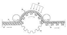
- FIG. 1is a schematic depiction of the electrophoretic display of the present invention.
- FIGS. 2 a and 2 bshow the roll to roll process for the manufacture of an electrophoretic display, in particular, the creation of microcups by embossing a conductor film coated with a UV curable composition.
- FIGS. 3 a - 3 dillustrate a typical method of preparing the male mold for microembossing.
- FIGS. 4 a - 4 cshow a typical microcup array prepared by microembossing.
- FIGS. 5 a - 5 cshow alternative processing steps for preparing the microcups involving imagewise exposure of the conductor film coated with a thermoset precursor to UV radiation.:
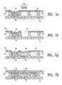
- FIG. 6is a flow chart for manufacturing a black/white electrophoretic display or other single color electrophoretic displays.
- FIGS. 7 a - 7 hare a flow chart for manufacturing a multi-color electrophoretic display.
- microcuprefers to the cup-like indentations created by microembossing or imagewise exposure.
- cellin the context of the present invention, is intended to mean the single unit formed from a sealed microcup.
- the cellsare filled with charged pigment particles dispersed in a solvent or solvent mixture.
- microcups or cellswhen describing the microcups or cells, is intended to indicate that the microcup or cell has a definite shape, size and aspect ratio which are pre-determined according to the specific parameters of the manufacturing process.
- aspect ratiois a commonly known term in the art of electrophoretic displays. In this application, it refers to the depth to width or depth to length ratio of the microcups.
- An electrophoretic display of the present inventionas shown in FIG. 1 , comprises two electrode plates ( 10 , 11 ), at least one of which is transparent ( 10 ), and a layer of well-defined cells ( 12 ) enclosed between the two electrodes.
- the cellsare of well-defined shape and size and are filled with charged pigment particles dispersed in a colored dielectric solvent.
- the charged particlesmigrate to one side, such that either the color of the pigment or the color of the solvent is seen through the transparent conductor film. At least one of the two conductors is patterned.
- the process for the preparation of such an electrophoretic displayinvolves several aspects.
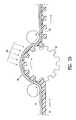
- the male mold ( 20 )may be placed either above ( FIG. 2 a ) or below ( FIG. 2 b ) the web ( 24 ).
- the transparent conductive substrateis constructed by forming a transparent conductor film ( 21 ) on a glass plate or a plastic substrate.
- a layer of a thermoplastic or thermoset precursor ( 22 )is then coated on the conductor film.
- the thermoplastic or thermoset precursor layeris embossed at a temperature higher than the glass transition temperature of the thermoplastic or thermoset precursor layer by the male mold in the form of a roller, plate or belt.
- the thermoplastic or thermoset precursor for the preparation of the microcupsmay be multifunctional acrylate or methacrylate, vinylether, epoxide and their oligomers, polymers and the like. Multifunctional acrylate and their oligomers are the most preferred. A combination of multifunctional epoxide and multifunctional acrylate is also very useful to achieve desirable physico-mechanical properties. A crosslinkable oligomer imparting flexibility, such as urethane acrylate or polyester acrylate, is usually also added to improve the flexure resistance of the embossed micro-cups.
- the compositionmay contain polymer, oligomer, monomer and additives or only oligomer, monomer and additives.
- the glass transition temperatures (or Tg) for this class of materialsusually range from about ⁇ 70° C. to about 150° C., preferably from about ⁇ 20° C. to about 50° C.
- the microembossing processis typically carried out at a temperature higher than the Tg.
- a heated male mold or a heated housing substrate against which the mold pressesmay be used to control the microembossing temperature and pressure.
- the moldis released during or after the precursor layer is hardened to reveal an array of microcups ( 23 ).
- the hardening of the precursor layermay be accomplished by cooling, cross-linking by radiation, heat or moisture. If the curing of the thermoset precursor is accomplished by UV radiation, UV may radiate onto the transparent conductor film from the bottom or the top of the web as shown in the two figures. Alternatively, UV lamps may be placed inside the mold. In this case, the mold must be transparent to allow the UV light to radiate through the pre-patterned male mold on to the thermoset precursor layer.
- the male moldmay be prepared by a photoresist process followed by either etching or electroplating.
- a representative example for the preparation of the male moldis given in FIG. 3 .
- a glass base ( 30 )is sputtered with a thin layer (typically 3000 ⁇ ) of a seed metal ( 31 ) such as chrome inconel. It is then coated with a layer of photoresist ( 32 ) and exposed to UV.
- a mask ( 34 )is placed between the UV and the layer of photoresist ( 32 ). The exposed areas of the photoresist become hardened. The unexposed areas are then removed by washing them with an appropriate solvent.
- a master( FIG. 3 b ) is then ready for electroforming.
- a typical material used for electroformingis nickel cobalt ( 33 ).
- the mastercan be made of nickel by nickel sulfamate electroforming or electroless nickel deposition as described in “Continuous manufacturing of thin cover sheet optical media”, SPIE Proc. Vol. 1663, pp.324 (1992).
- the floor of the mold( FIG. 3 d ) is typically between 50 to 400 microns.
- the mastercan also be made using other microengineering techniques including e-beam writing, dry etching, chemical etching, laser writing or laser interference as described in “Replication techniques for micro-optics”, SPIE Proc. Vol.3099, pp76-82 (1997).
- the moldcan be made by photomachining using plastics, ceramics or metals.
- FIG. 4 ais an optical profilometry three-dimensional profile of the typical microcups prepared by microembossing.
- FIG. 4 bis an optical microscopic picture showing the openings of the microcups from the top view.
- FIG. 4 cis the optical profilometry vertical cross-section view of a row of microcups showing their depth.
- the microcupsmay be prepared by imagewise exposure ( FIG. 5 a ) of a radiation curable material ( 51 ) coated on the conductor film ( 52 ) to UV or other forms of radiation through a mask ( 50 ).
- the conductor film ( 52 )is on a plastic substrate ( 53 ).
- the photomaskmay be synchronized with the web and move at the same speed as the latter.
- the dark squares ( 54 )represent the opaque area and the space ( 55 ) between the dark squares represents the opening area.
- the UVradiates through the opening area ( 55 ) onto the radiation curable material.
- the exposed areasbecome hardened and the unexposed areas (protected by the opaque area in the mask) are then removed by an appropriate solvent or developer to form the microcups ( 56 ).
- the solvent or developeris selected from those commonly used for dissolving or reducing the viscosity of radiation curable materials such as methylethylketone, toluene, acetone, isopropanol or the like.
- FIGS. 5 b and 5 cillustrate two other options for the preparation of microcups by imagewise exposure.
- the conductor film ( 52 ) usedis opaque and pre-patterned. In this case, it may be advantageous to imagewise expose the radiation sensitive material through the conductor pattern which serves as the photomask.
- the microcups ( 56 )can then be formed by removing the unexposed areas after UV radiation.
- the conductor film ( 52 )is also opaque and line-patterned.
- the radiation curable materialis exposed from the bottom through the conductor line pattern ( 52 ) which serves as the first photomask.
- a second exposureis performed from the other side through the second photomask ( 50 ) having a line pattern perpendicular to the conductor lines.
- the unexposed areais then removed by a solvent or developer to reveal the microcups ( 56 ).
- the microcupscan be of any shape, and their sizes and shapes may vary.
- the microcupsmay be of substantially uniform size and shape in one system.
- microcups having a mixture of different shapes and sizesmay be produced.
- microcups filled with a dispersion of the red colormay have a different shape or size from the green microcups or the blue microcups.
- a pixelmay consist of different numbers of microcups of different colors.
- a pixelmay consist of a number of small green microcups, a number of large red microcups, and a number of small blue microcups. It is not necessary to have the same shape and number for the three colors.
- the openings of the microcupsmay be round, square, rectangular, hexagonal, or any other shape.
- the partition area between the openingsis preferably kept small in order to achieve a high color saturation and contrast while maintaining desirable mechanical properties. Consequently the honeycomb-shaped opening is preferred over, for example, the circular opening.
- each individual microcupmay be in the range of about 10 2 to about 5 ⁇ 10 5 ⁇ m 2 , preferably from about 10 3 about 5 ⁇ 10 4 ⁇ m 2 .
- the depth of the microcupsis in the range of about 3 to about 100 microns, preferably from about 10 to about 50 microns.
- the opening to wall ratiois in the range of from about 0.05 to about 100, preferably from about 0.4 to about 20.
- the distances of the openingsusually are in the range of from about 15 to about 450 microns, preferably from about 25 to about 300 microns from edge to edge of the openings.
- the microcupsare filled with charged pigment particles dispersed in a dielectric solvent.
- the dispersionmay be prepared according to methods well known in the art such as U.S. Pat. Nos. 6,017,584, 5,914,806, 5,573,711, 5,403,518, 5,380,362, 4,680,103, 4,285,801, 4,093,534, 4,071,430, 3,668,106 and IEEE Trans. Electron Devices , ED-24, 827 (1977), and J. Appl. Phys . 49(9), 4820 (1978).
- the charged pigment particlesvisually contrast with the medium in which the particles are suspended.
- the mediumis a dielectric solvent which preferably has a low viscosity and a dielectric constant in the range of about 2 to about 30, preferably about 2 to about 15 for high particle mobility.
- suitable dielectric solventsinclude hydrocarbons such as decahydronaphthalene (DECALIN), 5-ethylidene-2-norbornene, fatty oils, paraffin oil, aromatic hydrocarbons such as toluene, xylene, phenylxylylethane, dodecylbenzene and alkylnaphthalene, halogenated solvents such as perfluorodecalin, perfluorotoluene, perfluoroxylene, dichlorobenzotrifluoride, 3,4,5-trichlorobenzotrifluoride, chloropentafluoro-benzene, dichlorononane, pentachlorobenzene, and perfluoro solvents such as FC-43, FC-70 and FC-5060 from 3M Company, St.
- halogen containing polymerssuch as poly(perfluoropropylene oxide) from TCI America, Portland, Oreg., poly(chlorotrifluoroethylene) such as Halocarbon Oils from Halocarbon Product Corp., River Edge, N.J., perfluoropolyalkylether such as Galden from Ausimont or Krytox Oils and Greases K-Fluid Series from DuPont, Del.
- poly(chlorotrifluoroethylene)is used as the dielectric solvent.
- poly(perfluoropropylene oxide)is used as the dielectric solvent.
- the suspending mediummay be colored by dyes or pigments.
- Nonionic azo and anthraquinone dyesare particularly useful. Examples of useful dyes include, but are not limited to: Oil Red EGN, Sudan Red, Sudan Blue, Oil Blue, Macrolex Blue, Solvent Blue 35, Pylam Spirit Black and Fast Spirit Black from Pylam Products Co., Arizona, Sudan Black B from Aldrich, Thermoplastic Black X-70 from BASF, anthroquinone blue, anthroquinone yellow 114, anthroquinone red 111, 135, anthroquinone green 28 from Aldrich.
- the pigment particles for generating the color of the mediummay also be dispersed in the dielectric medium. These color particles are preferably uncharged.
- the pigment particles for generating color in the mediumare charged, they preferably carry a charge which is opposite from that of the charged pigment particles. If both types of pigment particles carry the same charge, then they should have different charge density or different electrophoretic mobility. In any case, the dye or pigment for generating color of the medium must be chemically stable and compatible with other components in the suspension.
- the charged pigment particlesmay be organic or inorganic pigments, such as TiO 2 , phthalocyanine blue, phthalocyanine green, diarylide yellow, diarylide AAOT Yellow, and quinacridone, azo, rhodamine, perylene pigment series from Sun Chemical, Hansa yellow G particles from Kanto Chemical, and Carbon Lampblack from Fisher. Submicron particle size is preferred.
- the particlesshould have acceptable optical characteristics, should not swollen or softened by the dielectric solvent, and should be chemically stable. The resulting suspension must also be stable against sedimentation, creaming or flocculation under normal operating conditions.
- the pigment particlesmay exhibit a native charge, or may be charged explicitly using a charge control agent, or may acquire a charge when suspended in the dielectric solvent.
- Suitable charge control agentsare well known in the art; they may be polymeric or non-polymeric in nature, and may al'so be ionic or non-ionic, including ionic surfactants such as Aerosol TO, sodium dodecylbenzenesulfonate, metal soap, polybutene succinimide, maleic anhydride copolymers, vinylpyridine copolymers, vinylpyrrolidone copolymer (such as Ganex from International Specialty Products), (meth)acrylic acid copolymers, N,N-dimethylaminoethyl (meth)acrylate copolymers.
- Fluorosurfactantsare particularly useful as charge controlling agents in perfluorocarbon solvents. These include FC fluorosurfactants such as FC-170C, FC-171, FC-176, FC430, FC431 and FC-740 from 3M Company and Zonyl fluorosurfactants such as Zonyl FSA, FSE, FSN, FSN-100, FSO, FSO-100, FSD and UR from Dupont.
- FC fluorosurfactantssuch as FC-170C, FC-171, FC-176, FC430, FC431 and FC-740 from 3M Company
- Zonyl fluorosurfactantssuch as Zonyl FSA, FSE, FSN, FSN-100, FSO, FSO-100, FSD and UR from Dupont.
- Suitable charged pigment dispersionsmay be manufactured by any of the well-known methods including grinding, milling, attriting, microfluidizing, and ultrasonic techniques. For example, pigment particles in the form of a fine powder are added to the suspending solvent and the resulting mixture is ball milled or attrited for several hours to break up the highly agglomerated dry pigment powder into primary particles. Although less preferred, a dye or pigment for generating color of the suspending medium may be added to the suspension during the ball milling process.
- Sedimentation or creaming of the pigment particlesmay be eliminated by microencapsulating the particles with suitable polymers to match the specific gravity to that of the dielectric solvent.
- Microencapsulation of the pigment particlesmay be accomplished chemically or physically. Typical microencapsulation processes include interfacial polymerization, in-situ polymerization, phase separation, coacervation, electrostatic coating, spray drying, fluidized bed coating and solvent evaporation.
- the suspensioncomprises charged white particles of titanium oxide (TiO 2 ) dispersed in a black solvent or charged black particles dispersed in a dielectric solvent.
- a black dye or dye mixturesuch as Pylam Spirit Black and Fast Spirit Black from Pylam Products Co. Arizona, Sudan Black B from Aldrich, Thermoplastic Black X-70 from BASF, or an insoluble black pigment such as carbon black may be used to generate the black color of the solvent.
- the charged TiO 2 particlesmay be suspended in a dielectric solvent of cyan, yellow or magenta color. The cyan, yellow or magenta color may be generated via the use of a dye or a pigment.
- the charged TiO 2 particlesmay be suspended in a dielectric solvent of red, green or blue color generated also via the use of a dye or a pigment. The red, green, blue color system is preferred for most applications.
- the sealing of the microcupsmay be accomplished in a number of ways.
- a preferred approachis to disperse a UV curable composition containing multifunctional acrylates, acrylated oligomers, and photoinitiators into an electrophoretic fluid containing charged pigment particles dispersed in a colored dielectric solvent.
- the UV curable compositionis immiscible with the dielectric solvent and has a specific gravity lower than that of the dielectric solvent and the pigment particles.
- the two components, UV curable composition and the electrophoretic fluidare thoroughly blended in an in-line mixer and immediately coated onto the microcups with a precision coating mechanism such as Myrad bar, gravure, doctor blade, slot coating or slit coating. Excess fluid is scraped away by a wiper blade or a similar device.
- a small amount of a weak solvent or solvent mixture such as isopropanol, methanol, or their aqueous solutionsmay be used to clean the, residual electrophoretic fluid on the top surface of the partition walls of the microcups.
- Volatile organic solventsmay be used to control the viscosity and coverage of the electrophoretic fluid.
- the thus-filled microcupsare then dried and the UV curable composition floats to the top of the electrophoretic fluid.
- the microcupsmay be sealed by curing the supernatant UV curable layer during or after it floats to the top. UV or other forms of radiation such as visible light, IR and electron beam may be used to cure and seal the microcups. Alternatively, heat or moisture may also be employed to cure and seal the microcups, if appropriate, heat or moisture curable compositions may be used.
- a preferred group of dielectric solvents exhibiting desirable density and solubility discrimination against acrylate monomers and oligomersare halogenated hydrocarbons and their derivatives.
- Surfactantsmay be used to improve the adhesion and wetting at the interface between the electrophoretic fluid and the sealing materials.
- Useful surfactantsinclude the FC surfactants from 3M Company, Zonyl fluorosurfactants from DuPont, fluoroacylates, fluoromethacrylates, fluoro-substituted long chain alcohols, perfluoro-substituted long chain carboxylic acids and their derivatives.
- the electrophoretic fluid and the sealing precursormay be coated sequentially into the microcups, if the sealing precursor is at least partially compatible with the dielectric solvent.
- the sealing of the microcupsmay be accomplished by overcoating a thin layer of thermoset precursor which is curable by radiation, heat, moisture or interfacial reactions and curing on the surface of the filled microcups. Interfacial polymerization followed by UV curing is very beneficial to the sealing process. Intermixing between the electrophoretic layer and the overcoat is significantly suppressed by the formation of a thin barrier layer at the interface by interfacial polymerization.
- the sealingis then completed by a post curing step, preferably by UV radiation.
- the specific gravity of the overcoatingis significantly lower than that of the electrophoretic fluid.
- Volatile organic solventsmay be used to adjust the viscosity and the thickness of the coatings. When a volatile solvent is used in the overcoat, it is preferred that it is immiscible with the dielectric solvent.
- the two-step overcoating processis particularly useful when the dye used is at least partially soluble in the thermoset precursor.
- the processis illustrated by the flow diagram as shown in FIG. 6 . All microcups are filled with a suspension of the same color composition.
- the processcan be a continuous roll-to-roll process comprising the following steps:
- the laminate adhesivemay be post cured by radiation such as UV ( 68 ) through the top conductor film if the latter is transparent to the radiation.
- the finished productmay be cut ( 69 ) after the lamination step.
- the preparation of the microcups described abovecan be conveniently replaced by the alternative procedure of imagewise exposing the conductor film coated with a thermoset precursor followed by removing the unexposed areas by an appropriate solvent.
- the sealing of the microcupsmay alternatively be accomplished by directly overcoating and curing a layer of the thermoset precursor composition over the surface of the electrophoretic fluid.
- additional stepsare needed to generate microcups containing suspensions of different colors. These additional steps include (1) laminating the already formed microcups with a positively working dry-film photoresist consisting of at least a removable support such as PET-4851 from Saint-Gobain, Worcester, Mass., a novolac positive photoresist such as Microposit S1118 from Shipley, and an alkali-developable adhesive layer such as a mixture of Nacor 72-8685 from National Starch and Carboset 515 from BF Goodrich; (2) selectively opening a certain amount of the microcups by imagewise exposing the photoresist, removing the removable support film, and developing the positive photoresist with a developer such as diluted Microposit 351 developer from Shipley; (3) filling the opened cups with the electrophoretic fluid containing charged white pigment (TiO 2 ) particles and dye or pigment of the first primary color; and (4) sealing the filled microcups as described in the preparation of monochrome
- a multi-color electrophoretic displaysmay be prepared according to the steps as shown in FIG. 7 :
- the preparation of the microcups described in the process abovecan conveniently be replaced by the alternative procedure of imagewise exposing the conductor film coated with a thermoset precursor followed by removing the unexposed areas by an appropriate solvent.
- the sealing of the microcupsmay be alternatively accomplished by directly coating a layer of the thermoset precursor material over the surface of the liquid phase.
- the thickness of the display produced by the present processes as describedcan be as thin as a piece of paper.
- the width of the displayis the width of the coating web (typically 3-90 inches).
- the length of the displaycan be anywhere from inches to thousands of feet depending on the size of the roll.
- composition shown in Table 1is coated onto Mylar J101/200 gauge using a Nickel Chrome bird type film applicator with an opening of 3 mil.
- the solventis allowed to evaporate leaving behind a tacky film with a Tg below room temperature.
- the coated filmwas then embossed by the stencil using a pressure roller at room temperature.
- the coatingwas then UV cured for about 20 minutes through the Mylar film using a Loctite Zeta 7410 exposure unit equipped with a metal fluoride lamp with an intensity of 80 mW/cm 2 at 365 nm.
- the embossed filmwas then released from the mold to reveal well-defined microcups having lateral dimensions ranging from 60 ⁇ m to 120 ⁇ m (200-400 dpi) and a depth ranging from 5 ⁇ m to 30 ⁇ m as measured by optical profilometry and microscope ( FIGS. 4 a - 4 c ).
- a composition containing solid oligomer, monomer and additiveis shown in Table 2.
- the glass transition temperature of the mixtureis again below room temperature.
- the tacky coatingis deposited on top of Mylar J101/200 gauge as before. Embossing can be conducted at 32° C. and 60° C. using a heated pressure roller or laminator. Well-defined high resolution microcups (100-400 dpi) with depth ranging from 5-30 microns were produced.
- Polystyrene(0.89 grams, Polysciences, Inc., mw. 50,000) and AOT (0.094 grams, American Cyanamide, sodium dioctylsulfosuccinate) were dissolved in 17.77 grams of hot xylene (Aldrich).
- Ti-Pure R-706(6.25 grams) was added to the solution and ground in an attritor at 200 rpm for more than 12 hours. A low viscosity, stable dispersion was obtained.
- Oil-blue N(0.25 grams, Aldrich) was added to color the dispersion. The suspension was then tested in a standard electrophoretic cell comprising two ITO conductor plates separated by a 24 microns spacer. High contrast, alternating white and blue images were observed with a switching rate of about 60 Hz and a rising time of 8.5 msec at 80 volts.
- Example 3The experiment of Example 3 was repeated, except Oil Red EGN (Aldrich) and an electrophoretic cell with a 24 micron spacer were used. High contrast, alternating red and white images were observed with a switching rate of 60 Hz and a rising time of 12 msec at 60 volts.
- Oil Red EGNAldrich
- an electrophoretic cell with a 24 micron spacerwere used. High contrast, alternating red and white images were observed with a switching rate of 60 Hz and a rising time of 12 msec at 60 volts.
- Ti-Pure R-706(1.12 grams) was ground by an attritor in a solution containing 11.2 grams of a maleic anhydride copolymer (Baker Hughes X-5231), 24 grams of 3,4-dichlorobenzotrifluoride, and 24 grams of 1,6-dichlorohexane (both from Aldrich). Similarly, 12 grams of carbon black were ground in a solution containing 1.2 grams of alkylated polyvinylpyrrolidone (Ganex V216 from ISP), 34 grams of 3,4-dichlorobenzotrifluoride, and 34 grams of 1,6-dichlorohexane (Aldrich) at 100° C. These two dispersions were then mixed homogeneously and tested. High contrast black and white images were observed with a switching rate up to 10 Hz and a rising time of about 36 msec at 100 volts.
- UV curable compositioncomprising 1 wt % of benzil dimethyl ketal (Esacure KB1 from Sartomer) in HDDA (1,6-hexanediol diacrylate from Aldrich) were dispersed into 0.4 ml of a dielectric solvent comprising 0.5 wt % of 2,2,3,3,4,4,5,5,6,6,7,7,8,8,9,9,10,10,10-nonadecafluoro-1-decanol (Aldrich) in FC-43 from 3M Company. The resultant dispersion was then immediately filled into an array of microcups as prepared in Example 2. Excess of fluid was scrapped away by a wiper blade. The HDDA solution was allowed to phase separate for at least 30 seconds and cured by UV radiation (10 mw/cm2) for about 1 minute. A hard, clear layer was observed on the top of the microcups and the microcups were sealed.
- the elctrophoretic fluid prepared in Example 5was coated onto the microcup array as prepared in Example 2.
- a thin layer of Norland optical adhesive NOA 60(Norland Products Inc., New Brunswick, N.J.) was coated onto the filled microcups. Any excess of the UV adhesive was scrapped off by a strip of Mylar film and cleaned by a piece of absorbing paper.
- the overcoated adhesivewas then cured immediately under a Loctite Zeta 7410 UV exposure unit for about 15 minutes. The microcups were sealed completely and no air pocket was observed.
- the thickness of cured adhesive layerwas about 5-10 microns as measured by a Mitutoyo thickness gauge.
- Example 7The experiment of Example 7 was repeated, except the Norland adhesive was replaced by Instant Krazy glue from Elmer's Products, Inc., Columbus, Ohio. The overcoated adhesive was then cured for 5 minutes by moisture in air. The microcups were sealed completely and no air pocket was observed. The thickness of cured adhesive layer was about 5-10 microns as measured by a Mitutoyo thickness gauge.
- Example 8The experiment of Example 8 was repeated, except the electrophoretic fluid was replaced by a 3,4-dichlorobenzotrifluoride solution containing 0.3 wt % of tetraethylenepentaamine (Aldrich) and the Instant Krazy glue was replaced by an aliphatic polyisocyanate (Desmodur N 3300 from Bayer Corp.) solution in anhydrous ether. A highly crosslinked thin film was observed almost immediately after overcoating. The dielectric solvent was completely sealed inside the microcups after ether was evaporated at room temperature. No air pocket was observed.
Landscapes
- Physics & Mathematics (AREA)
- Nonlinear Science (AREA)
- Optics & Photonics (AREA)
- General Physics & Mathematics (AREA)
- Chemical & Material Sciences (AREA)
- Electrochemistry (AREA)
- Molecular Biology (AREA)
- Health & Medical Sciences (AREA)
- Chemical Kinetics & Catalysis (AREA)
- Life Sciences & Earth Sciences (AREA)
- Mathematical Physics (AREA)
- Crystallography & Structural Chemistry (AREA)
- Electrochromic Elements, Electrophoresis, Or Variable Reflection Or Absorption Elements (AREA)
- Processes Of Treating Macromolecular Substances (AREA)
- Eye Examination Apparatus (AREA)
- Devices For Indicating Variable Information By Combining Individual Elements (AREA)
Abstract
Description
- 1. Coat a layer of thermoplastic or thermoset precursor (60) optionally with a solvent on a conductor film (61). The solvent, if present, readily evaporates.
- 2. Emboss the thermoplastic or thermoset precursor layer at a temperature higher than the glass transition temperature of the thermoset precursor layer by a pre-patterned male mold (62).
- 3. Release the mold from the thermoplastic or thermoset precursor layer preferably during or after it is hardened by proper means.
- 4. Fill in the thus-formed array of microcups (63) with a charged pigment dispersion (64) in a colored dielectric solvent containing at least a thermoset precursor which is incompatible with the solvent and has a lower specific gravity than the solvent and the pigment particles.
- 5. Seal the microcups by curing the thermoset precursor preferably by radiation such as UV (65), or by heat or moisture during or after the thermoset precursor separates and forms a supernatant layer on top of the liquid phase, thus forming closed electrophoretic cells containing pigment dispersion in a colored dielectric solvent.
- 6. Laminate the sealed array of electrophoretic cells with a second conductor film (66) pre-coated with an adhesive layer (67) which may be a pressure sensitive adhesive, a hot melt adhesive, a heat, moisture, or radiation curable adhesive.
- 1. Coat a layer of thermoset precursor (70) on a conductor film (71).
- 2. Emboss the thermoplastic or thermoset precursor layer at a temperature higher than its glass transition temperature by a pre-patterned male mold (not shown).
- 3. Release the mold from the thermoplastic or thermoset precursor layer preferably during or after it is hardened by cooling or crosslinking by radiation, heat or moisture.
- 4. Laminate the thus formed array of microcups (72) with a positive dry-film photoresist which comprises at least an adhesive layer (73), a positive photoresist (74) and a removable plastic cover sheet (not shown).
- 5. Imagewise expose (
FIG. 7 c) the positive photoresist by UV, visible light, or other radiation, remove the cover sheet, develop and open cups in the exposed area. The purpose of Steps 4 and 5 is to selectively open the microcups in a predetermined area (FIG. 7 d). - 6. Fill in the opened microcups with a charged white pigment dispersion (75) in a dielectric solvent containing at least a dye or pigment of the first primary color and a thermoset precursor (76) which is incompatible with the solvent and has a lower specific gravity than the solvent and the pigment particles.
- 7. Seal the microcups to form closed electrophoretic cells containing electrophoretic fluid of the first primary color by curing the thermoset precursor (preferably by radiation such as UV, less preferably by heat or moisture) during or after the thermoset precursor separates and forms a supernatant layer on top of the liquid phase (
FIG. 7 e). - 8. Steps 5-7 described above may be repeated to generate well-defined cells containing electrophoretic fluids of different colors in different areas (
FIGS. 7 e,7fand7g). - 9. Laminate the sealed array of electrophoretic cells in registration to a second, pre-patterned transparent conductor film (77) pre-coated with an adhesive layer (78) which may be a pressure sensitive adhesive, a hot melt adhesive, a heat, moisture, or radiation curable adhesive.
- 10. Harden the adhesive.
| TABLE 1 |
| PMMA-containing composition for microembossing |
| No. | Description | Ingredient | Wt % | ||
| 1 | Epoxy acrylate | Ebecryl 3605 | UCB Chemicals | 7.35 |
| 2 | Monomer | Sartomer SR205 | Sartomer | 9.59 |
| 3 | Urethane | Ebecryl 6700 | UCB Chemicals | 4.87 |
| acrylate | ||||
| 4 | Polymethyl- | Elvacite 2051 | ICI | 9.11 |
| methacrylate | ||||
| 5 | Photoinitiator | Darocur 1173 | Ciba | 1.45 |
| 6 | Cationic | Cyracure UVI 6976 | Union Carbide | 0.60 |
| photoinitiator | ||||
| 7 | Solvent | Acetone | Aldrich | 67.03 |
| Total | 100.00 | |||
| TABLE 2 |
| Embossing composition containing oligomer, monomer, |
| additive and solvent |
| No. | Description | Ingredient | Wt % | ||
| 1 | Epoxy acrylate | Ebecryl 3903 | UCB Chemicals | 17.21 |
| 2 | Monomer | HDODA | UCB Chemicals | 8.61 |
| 3 | Urethane acrylate | Ebecryl 4827 | UCB Chemicals | 2.87 |
| 4 | Photoinitiator | Irgacure 500 | Ciba | 1.43 |
| 5 | Slip | Ebecryl 1360 | UCB Chemicals | 1.60 |
| 6 | Solvent | Acetone | Aldrich | 68.26 |
| Total | 100 | |||
Claims (30)
Priority Applications (49)
| Application Number | Priority Date | Filing Date | Title |
|---|---|---|---|
| US09/518,488US6930818B1 (en) | 2000-03-03 | 2000-03-03 | Electrophoretic display and novel process for its manufacture |
| US09/606,654US6672921B1 (en) | 2000-03-03 | 2000-06-28 | Manufacturing process for electrophoretic display |
| US09/784,972US6933098B2 (en) | 2000-01-11 | 2001-02-15 | Process for roll-to-roll manufacture of a display by synchronized photolithographic exposure on a substrate web |
| TW090104838ATWI238917B (en) | 2000-03-03 | 2001-03-02 | An improved electrophoretic display and novel process for its manufacture |
| MXPA02008517AMXPA02008517A (en) | 2000-03-03 | 2001-03-05 | Electrophoretic display. |
| HK02109031.0AHK1047477B (en) | 2000-03-03 | 2001-03-05 | An electrophoretic display sealed with a way and process for its manufacture |
| CA002401564ACA2401564C (en) | 2000-03-03 | 2001-03-05 | An improved electrophoretic display and novel process for its manufacture |
| EP04025496AEP1500970A1 (en) | 2000-03-03 | 2001-03-05 | Electrophoretic display |
| CNB2004100327522ACN100368922C (en) | 2000-03-03 | 2001-03-05 | Method for making a multicolor electrophoretic display |
| CNB018002277ACN1174281C (en) | 2000-03-03 | 2001-03-05 | Electrophoretic display sealed by a method and method of manufacturing the same |
| KR1020027011387AKR100566417B1 (en) | 2000-03-03 | 2001-03-05 | Method of manufacturing electrophoretic display |
| AU2001240036AAU2001240036A1 (en) | 2000-03-03 | 2001-03-05 | Electrophoretic display |
| DE60107396TDE60107396T2 (en) | 2000-03-03 | 2001-03-05 | ELECTROPHORETIC DISPLAY |
| PCT/US2001/006917WO2001067170A1 (en) | 2000-03-03 | 2001-03-05 | Electrophoretic display |
| EP01914676AEP1264210B1 (en) | 2000-03-03 | 2001-03-05 | Electrophoretic display |
| AT01914676TATE283499T1 (en) | 2000-03-03 | 2001-03-05 | ELECTROPHORETIC DISPLAY |
| JP2001566087AJP3680996B2 (en) | 2000-03-03 | 2001-03-05 | Electrophoresis display |
| US09/942,532US6788449B2 (en) | 2000-03-03 | 2001-08-29 | Electrophoretic display and novel process for its manufacture |
| US10/087,527US6859302B2 (en) | 2000-03-03 | 2002-02-28 | Electrophoretic display and novel process for its manufacture |
| US10/092,936US6831770B2 (en) | 2000-03-03 | 2002-03-06 | Electrophoretic display and novel process for its manufacture |
| US10/179,997US6833943B2 (en) | 2000-03-03 | 2002-06-24 | Electrophoretic display and novel process for its manufacture |
| US10/198,729US6885495B2 (en) | 2000-03-03 | 2002-07-16 | Electrophoretic display with in-plane switching |
| US10/237,522US6751008B2 (en) | 2000-03-03 | 2002-09-06 | Electrophoretic display and novel process for its manufacture |
| HK02109029.4AHK1048363A1 (en) | 2000-01-11 | 2002-12-12 | Process for roll-to-roll manufacture of a display by synchronized photolithographic exposure on a substrate web |
| US10/351,460US7158282B2 (en) | 2000-03-03 | 2003-01-24 | Electrophoretic display and novel process for its manufacture |
| US10/372,027US6829078B2 (en) | 2000-03-03 | 2003-02-21 | Electrophoretic display and novel process for its manufacture |
| US10/388,890US20030179437A1 (en) | 2000-03-03 | 2003-03-14 | Electrophoretic display and novel process for its manufacture |
| KR1020030018882AKR100641611B1 (en) | 2000-03-03 | 2003-03-26 | Process for manufacturing electrophoretic display |
| KR1020030018885AKR100572547B1 (en) | 2000-03-03 | 2003-03-26 | Electrophoretic display |
| KR1020030018883AKR100561897B1 (en) | 2000-03-03 | 2003-03-26 | Electrophoretic display |
| JP2003113086AJP5204942B2 (en) | 2000-03-03 | 2003-04-17 | Electrophoresis display |
| US10/444,760US6867898B2 (en) | 2000-03-03 | 2003-05-23 | Electrophoretic display and novel process for its manufacture |
| US10/812,697US6865012B2 (en) | 2000-03-03 | 2004-03-29 | Electrophoretic display and novel process for its manufacture |
| US10/819,237US6987605B2 (en) | 2000-03-03 | 2004-04-05 | Transflective electrophoretic display |
| US10/841,122US7408696B2 (en) | 2000-03-03 | 2004-05-07 | Three-dimensional electrophoretic displays |
| US10/845,295US7052571B2 (en) | 2000-03-03 | 2004-05-12 | Electrophoretic display and process for its manufacture |
| US10/851,888US6947202B2 (en) | 2000-03-03 | 2004-05-20 | Electrophoretic display with sub relief structure for high contrast ratio and improved shear and/or compression resistance |
| US11/031,413US7233429B2 (en) | 2000-03-03 | 2005-01-07 | Electrophoretic display |
| US11/115,645US7142351B2 (en) | 2000-03-03 | 2005-04-26 | Electro-magnetophoresis display |
| US11/202,437US7522332B2 (en) | 2000-03-03 | 2005-08-10 | Electrophoretic display and process for its manufacture |
| US11/293,194US7112114B2 (en) | 2000-03-03 | 2005-12-01 | Electrophoretic display and process for its manufacture |
| US11/392,242US7557981B2 (en) | 2000-03-03 | 2006-03-28 | Electrophoretic display and process for its manufacture |
| US11/408,622US7715087B2 (en) | 2000-03-03 | 2006-04-21 | Segment electrophoretic displays and methods for their manufacture |
| US11/545,091US7576904B2 (en) | 2000-03-03 | 2006-10-06 | Electro-magnetophoresis display |
| US11/562,888US20070237962A1 (en) | 2000-03-03 | 2006-11-22 | Semi-finished display panels |
| US11/741,682US7715088B2 (en) | 2000-03-03 | 2007-04-27 | Electrophoretic display |
| US12/752,881US8520292B2 (en) | 2000-03-03 | 2010-04-01 | Electrophoretic display and process for its manufacture |
| US13/027,100US8582197B2 (en) | 2000-03-03 | 2011-02-14 | Process for preparing a display panel |
| US13/974,980US9081250B2 (en) | 2000-03-03 | 2013-08-23 | Electrophoretic display and process for its manufacture |
Applications Claiming Priority (1)
| Application Number | Priority Date | Filing Date | Title |
|---|---|---|---|
| US09/518,488US6930818B1 (en) | 2000-03-03 | 2000-03-03 | Electrophoretic display and novel process for its manufacture |
Related Parent Applications (1)
| Application Number | Title | Priority Date | Filing Date |
|---|---|---|---|
| US09/759,212Continuation-In-PartUS6795138B2 (en) | 2001-01-11 | 2001-01-11 | Transmissive or reflective liquid crystal display and novel process for its manufacture |
Related Child Applications (18)
| Application Number | Title | Priority Date | Filing Date |
|---|---|---|---|
| US09/606,654Continuation-In-PartUS6672921B1 (en) | 2000-01-11 | 2000-06-28 | Manufacturing process for electrophoretic display |
| US09/784,972Continuation-In-PartUS6933098B2 (en) | 2000-01-11 | 2001-02-15 | Process for roll-to-roll manufacture of a display by synchronized photolithographic exposure on a substrate web |
| US09/942,532Continuation-In-PartUS6788449B2 (en) | 2000-03-03 | 2001-08-29 | Electrophoretic display and novel process for its manufacture |
| US10/087,527ContinuationUS6859302B2 (en) | 2000-03-03 | 2002-02-28 | Electrophoretic display and novel process for its manufacture |
| US10/092,936Continuation-In-PartUS6831770B2 (en) | 2000-03-03 | 2002-03-06 | Electrophoretic display and novel process for its manufacture |
| US10/179,997Continuation-In-PartUS6833943B2 (en) | 2000-03-03 | 2002-06-24 | Electrophoretic display and novel process for its manufacture |
| US10/198,729Continuation-In-PartUS6885495B2 (en) | 2000-03-03 | 2002-07-16 | Electrophoretic display with in-plane switching |
| US10/229,530Continuation-In-PartUS6795229B2 (en) | 2000-03-03 | 2002-08-27 | Electrophoretic display with sub relief structure for high contrast ratio and improved shear and/or compression resistance |
| US10/243,280Continuation-In-PartUS20030048522A1 (en) | 2000-03-03 | 2002-09-12 | Three-dimensional electrophoretic displays |
| US10/351,460Continuation-In-PartUS7158282B2 (en) | 2000-03-03 | 2003-01-24 | Electrophoretic display and novel process for its manufacture |
| US10/421,217Continuation-In-PartUS6914713B2 (en) | 2000-03-03 | 2003-04-22 | Electro-magnetophoresis display |
| US10/444,760ContinuationUS6867898B2 (en) | 2000-03-03 | 2003-05-23 | Electrophoretic display and novel process for its manufacture |
| US10/819,237Continuation-In-PartUS6987605B2 (en) | 2000-03-03 | 2004-04-05 | Transflective electrophoretic display |
| US10/841,122Continuation-In-PartUS7408696B2 (en) | 2000-03-03 | 2004-05-07 | Three-dimensional electrophoretic displays |
| US10/845,295Continuation-In-PartUS7052571B2 (en) | 2000-03-03 | 2004-05-12 | Electrophoretic display and process for its manufacture |
| US10/851,888Continuation-In-PartUS6947202B2 (en) | 2000-03-03 | 2004-05-20 | Electrophoretic display with sub relief structure for high contrast ratio and improved shear and/or compression resistance |
| US11/115,645Continuation-In-PartUS7142351B2 (en) | 2000-03-03 | 2005-04-26 | Electro-magnetophoresis display |
| US11/545,091Continuation-In-PartUS7576904B2 (en) | 2000-03-03 | 2006-10-06 | Electro-magnetophoresis display |
Publications (1)
| Publication Number | Publication Date |
|---|---|
| US6930818B1true US6930818B1 (en) | 2005-08-16 |
Family
ID=24064141
Family Applications (4)
| Application Number | Title | Priority Date | Filing Date |
|---|---|---|---|
| US09/518,488Expired - LifetimeUS6930818B1 (en) | 2000-01-11 | 2000-03-03 | Electrophoretic display and novel process for its manufacture |
| US10/087,527Expired - LifetimeUS6859302B2 (en) | 2000-03-03 | 2002-02-28 | Electrophoretic display and novel process for its manufacture |
| US10/237,522Expired - LifetimeUS6751008B2 (en) | 2000-03-03 | 2002-09-06 | Electrophoretic display and novel process for its manufacture |
| US10/444,760Expired - LifetimeUS6867898B2 (en) | 2000-03-03 | 2003-05-23 | Electrophoretic display and novel process for its manufacture |
Family Applications After (3)
| Application Number | Title | Priority Date | Filing Date |
|---|---|---|---|
| US10/087,527Expired - LifetimeUS6859302B2 (en) | 2000-03-03 | 2002-02-28 | Electrophoretic display and novel process for its manufacture |
| US10/237,522Expired - LifetimeUS6751008B2 (en) | 2000-03-03 | 2002-09-06 | Electrophoretic display and novel process for its manufacture |
| US10/444,760Expired - LifetimeUS6867898B2 (en) | 2000-03-03 | 2003-05-23 | Electrophoretic display and novel process for its manufacture |
Country Status (13)
| Country | Link |
|---|---|
| US (4) | US6930818B1 (en) |
| EP (2) | EP1264210B1 (en) |
| JP (2) | JP3680996B2 (en) |
| KR (4) | KR100566417B1 (en) |
| CN (2) | CN1174281C (en) |
| AT (1) | ATE283499T1 (en) |
| AU (1) | AU2001240036A1 (en) |
| CA (1) | CA2401564C (en) |
| DE (1) | DE60107396T2 (en) |
| HK (1) | HK1047477B (en) |
| MX (1) | MXPA02008517A (en) |
| TW (1) | TWI238917B (en) |
| WO (1) | WO2001067170A1 (en) |
Cited By (206)
| Publication number | Priority date | Publication date | Assignee | Title |
|---|---|---|---|---|
| US20020185788A1 (en)* | 2001-03-30 | 2002-12-12 | Kenji Otokawa | Method for producing resin-molded substrate and method for producing reversible image display medium |
| US20030132925A1 (en)* | 2002-01-16 | 2003-07-17 | Pinyen Lin | Spacer layer for electrophoretic display device |
| US20030203101A1 (en)* | 2002-04-24 | 2003-10-30 | Sipix Imaging, Inc. | Process for forming a patterned thin film conductive structure on a substrate |
| US20040112525A1 (en)* | 2002-09-04 | 2004-06-17 | Cheri Pereira | Adhesive and sealing layers for electrophoretic displays |
| US20040120024A1 (en)* | 2002-09-23 | 2004-06-24 | Chen Huiyong Paul | Electrophoretic displays with improved high temperature performance |
| US20040131779A1 (en)* | 2002-04-24 | 2004-07-08 | Sipix Imaging, Inc. | Process for forming a patterned thin film structure on a substrate |
| US20040216837A1 (en)* | 2002-09-04 | 2004-11-04 | Cheri Pereira | Adhesive and sealing layers for electrophoretic displays |
| US20050007648A1 (en)* | 2003-07-10 | 2005-01-13 | Wu Zarng-Arh George | Methods and compositions for improved electrophoretic display performance |
| US20050099575A1 (en)* | 2001-01-11 | 2005-05-12 | Rong-Chang Liang | Transmissive or reflective liquid crystal display and process for its manufacture |
| US20050163940A1 (en)* | 2003-06-06 | 2005-07-28 | Sipix Imaging, Inc. | In mold manufacture of an object with embedded display panel |
| US20050189524A1 (en)* | 2004-02-23 | 2005-09-01 | Xin Weng | Modification of electrical properties of display cells for improving electrophoretic display performance |
| US20050195470A1 (en)* | 2002-10-21 | 2005-09-08 | Toshihiko Takeda | Process for producing display device |
| US20050243406A1 (en)* | 2000-03-03 | 2005-11-03 | Jerry Chung | Electro-magnetophoresis display |
| US20050259313A1 (en)* | 2004-05-12 | 2005-11-24 | Xiaojia Wang | Process for the manufacture of electrophoretic displays |
| US20060033981A1 (en)* | 2004-08-13 | 2006-02-16 | Yi-Shung Chaug | Direct drive display with a multi-layer backplane and process for its manufacture |
| US20060127667A1 (en)* | 2002-01-03 | 2006-06-15 | Zang Hongmei | Functionalized halogenated polymers for microencapsulation |
| US20060125779A1 (en)* | 2001-08-17 | 2006-06-15 | Rong-Chang Liang | Electrophoretic display with dual-mode switching |
| US20060132428A1 (en)* | 2004-12-17 | 2006-06-22 | Liu John H | Backplane design for display panels and processes for their manufacture |
| US20060132896A1 (en)* | 2002-02-11 | 2006-06-22 | Hsu Wan P | Core-shell particles for electrophoretic display |
| US20060164715A1 (en)* | 2000-03-03 | 2006-07-27 | Rong-Chang Liang | Electrophoretic display and process for its manufacture |
| US20060215106A1 (en)* | 2005-03-14 | 2006-09-28 | Kang Gary Y | Design and manufacturing processes of backplane for segment displays |
| US20060228532A1 (en)* | 2005-04-08 | 2006-10-12 | Chenhang Sun | Reflective displays and processes for their manufacture |
| US20060255322A1 (en)* | 2002-07-17 | 2006-11-16 | Wu Zarng-Arh G | Methods and compositions for improved electrophoretic display performance |
| US20060262249A1 (en)* | 2001-01-11 | 2006-11-23 | Rong-Chang Liang | Transmissive or reflective liquid crystal display and process for its manufacture |
| US20060262384A1 (en)* | 2003-10-07 | 2006-11-23 | Jerry Chung | Electrophoretic display with thermal control |
| US20060281924A1 (en)* | 2003-08-08 | 2006-12-14 | Jin Yang | Fluorinated dyes or colorants and their uses |
| US20060291064A1 (en)* | 2005-06-24 | 2006-12-28 | Industrial Technology Research Institute | Optical film with array of microstructures and the light source apparatus utilizing the same |
| US20070036919A1 (en)* | 2003-01-24 | 2007-02-15 | Xiaojia Wang | Adhesive and sealing layers for electrophoretic displays |
| US20070035497A1 (en)* | 2002-09-23 | 2007-02-15 | Chen Huiyong P | Electrophoretic displays with improved high temperature performance |
| US20070042135A1 (en)* | 2002-11-25 | 2007-02-22 | Rong-Chang Liang | Transmissive or reflective liquid crystal display |
| US20070057908A1 (en)* | 1996-07-19 | 2007-03-15 | E Ink Corporation | Electronically addressable microencapsulated ink and display thereof |
| US20070070030A1 (en)* | 2005-09-23 | 2007-03-29 | Zang Hongmei | Display cell structure and electrode protecting layer compositions |
| US20070070032A1 (en)* | 2004-10-25 | 2007-03-29 | Sipix Imaging, Inc. | Electrophoretic display driving approaches |
| US20070076289A1 (en)* | 2005-09-28 | 2007-04-05 | Xiaojia Wang | Electrophoretic display and methods of addressing such display |
| US20070121194A1 (en)* | 2005-11-09 | 2007-05-31 | Seiko Epson Corporation | Manufacturing method of electrophoretic display sheet, manufacturing method of electrophoretic display device, electrophoretic display device, and electronic apparatus |
| US20070134825A1 (en)* | 2005-12-13 | 2007-06-14 | Industrial Technology Research Institute | Non-mask micro-flow etching process |
| US20070153360A1 (en)* | 2002-03-21 | 2007-07-05 | Ching-Shon Ho | Magnetophoretic and electromagnetophoretic displays |
| US20070160762A1 (en)* | 2002-04-24 | 2007-07-12 | Yi-Shung Chaug | Process for forming a patterned thin film structure for in-mold decoration |
| US20070187654A1 (en)* | 2002-10-10 | 2007-08-16 | Jack Hou | Method for inducing or enhancing the threshold voltage of an electrophoretic display |
| US20070243332A1 (en)* | 2001-06-04 | 2007-10-18 | Zang Hongmei | Composition and process for the sealing of microcups in roll-to-roll display manufacturing |
| US20070263277A1 (en)* | 2001-08-17 | 2007-11-15 | Rong-Chang Liang | Electrophoretic display with dual mode switching |
| US20070268567A1 (en)* | 2000-03-03 | 2007-11-22 | Jerry Chung | Electro-magnetophoresis display |
| US20070296452A1 (en)* | 2006-05-26 | 2007-12-27 | Kang Gary Y | Flexible display testing and inspection |
| US20080020007A1 (en)* | 2006-07-18 | 2008-01-24 | Zang Hongmei | Liquid-containing film structure |
| US20080041967A1 (en)* | 2002-05-29 | 2008-02-21 | Jerry Chung | Electrode and connecting designs for roll-to-roll format-flexible display manufacturing |
| US20080075839A1 (en)* | 2002-04-24 | 2008-03-27 | Haubrich Jeanne E | Process for forming a patterned thin film structure on a substrate |
| US20080149271A1 (en)* | 2006-11-17 | 2008-06-26 | Jun Qi | Post conversion methods for display devices |
| US20080169821A1 (en)* | 2006-04-07 | 2008-07-17 | Wanheng Wang | Inspection methods for defects in electrophoretic display and related devices |
| US20080173719A1 (en)* | 2007-01-19 | 2008-07-24 | Chein-Hsun Wang | Temperature management in an integrated circuit card with electrophoretic display |
| US20080218471A1 (en)* | 2003-10-07 | 2008-09-11 | Jerry Chung | Electrophoretic display with thermal control |
| US20080303780A1 (en)* | 2007-06-07 | 2008-12-11 | Sipix Imaging, Inc. | Driving methods and circuit for bi-stable displays |
| WO2008133515A3 (en)* | 2007-04-25 | 2009-01-15 | Polymer Vision Ltd | Fabrication of planar electronic circuit devices |
| US20090268274A1 (en)* | 2007-06-01 | 2009-10-29 | Masahiro Masuzawa | Electrophoretic fluid, electrophoretic display medium, electrophoretic display element, and electrophoretic display device |
| US20090267970A1 (en)* | 2008-04-25 | 2009-10-29 | Sipix Imaging, Inc. | Driving methods for bistable displays |
| US20090273827A1 (en)* | 2008-05-01 | 2009-11-05 | Craig Lin | Color display devices |
| KR100929486B1 (en)* | 2007-09-11 | 2009-12-02 | 에스케이씨하스디스플레이필름(유) | Optical element for display device |
| US20100027073A1 (en)* | 2008-08-01 | 2010-02-04 | Craig Lin | Gamma adjustment with error diffusion for electrophoretic displays |
| US20100033803A1 (en)* | 2003-01-24 | 2010-02-11 | Xiaojia Wang | Adhesive and sealing layers for electrophoretic displays |
| US20100053728A1 (en)* | 2008-09-02 | 2010-03-04 | Craig Lin | Color display devices |
| US20100103501A1 (en)* | 2008-10-28 | 2010-04-29 | Xiaojia Wang | Electrophoretic display structures |
| US20100129527A1 (en)* | 2007-03-08 | 2010-05-27 | Ricoh Company, Ltd. | Manufacturing method and manufacturing apparatus for image display element structure, and manufacturing method and manufacturing apparatus for electrophoretic image display element |
| US20100134538A1 (en)* | 2008-10-24 | 2010-06-03 | Sprague Robert A | Driving methods for electrophoretic displays |
| US20100141573A1 (en)* | 2008-12-05 | 2010-06-10 | Craig Lin | Luminance enhancement structure with moire reducing design |
| US20100165005A1 (en)* | 2008-12-30 | 2010-07-01 | Sprague Robert A | Highlight color display architecture using enhanced dark state |
| US20100165448A1 (en)* | 2008-12-30 | 2010-07-01 | Sprague Robert A | Multicolor display architecture using enhanced dark state |
| US20100177396A1 (en)* | 2009-01-13 | 2010-07-15 | Craig Lin | Asymmetrical luminance enhancement structure for reflective display devices |
| US20100182351A1 (en)* | 2009-01-22 | 2010-07-22 | Craig Lin | Luminance enhancement structure with varying pitches |
| US20100188731A1 (en)* | 2007-03-08 | 2010-07-29 | Toshihiro Kanematsu | Display element, image display device, and image display system |
| US20100225999A1 (en)* | 2009-03-09 | 2010-09-09 | Craig Lin | Luminance enhancement structure for reflective display devices |
| US20100271408A1 (en)* | 2009-04-22 | 2010-10-28 | Feng-Shou Lin | Partial update driving methods for electrophoretic displays |
| US20100271407A1 (en)* | 2009-04-22 | 2010-10-28 | Andrew Ho | Reflective display devices with luminance enhancement film |
| US7830592B1 (en) | 2007-11-30 | 2010-11-09 | Sipix Imaging, Inc. | Display devices having micro-reflectors |
| US20100283804A1 (en)* | 2009-05-11 | 2010-11-11 | Sipix Imaging, Inc. | Driving Methods And Waveforms For Electrophoretic Displays |
| US20100288639A1 (en)* | 2004-05-12 | 2010-11-18 | Xiaojia Wang | Process for the manufacture of electrophoretic displays |
| US20100295880A1 (en)* | 2008-10-24 | 2010-11-25 | Sprague Robert A | Driving methods for electrophoretic displays |
| US20110026098A1 (en)* | 2009-07-29 | 2011-02-03 | Seiko Epson Corporation | Electrophoretic Display Element, Electrophoretic Display Device, and Electronic Apparatus |
| US20110043543A1 (en)* | 2009-08-18 | 2011-02-24 | Hui Chen | Color tuning for electrophoretic display |
| US20110063314A1 (en)* | 2009-09-15 | 2011-03-17 | Wen-Pin Chiu | Display controller system |
| US20110080362A1 (en)* | 2009-10-05 | 2011-04-07 | Sprague Robert A | Electronic information displays |
| US20110157682A1 (en)* | 2005-09-23 | 2011-06-30 | Zang Hongmei | Display cell structure and electrode protecting layer compositions |
| US20110226998A1 (en)* | 2008-09-19 | 2011-09-22 | Liquavista B.V. | Electrowetting elements |
| US8237892B1 (en) | 2007-11-30 | 2012-08-07 | Sipix Imaging, Inc. | Display device with a brightness enhancement structure |
| US8243013B1 (en) | 2007-05-03 | 2012-08-14 | Sipix Imaging, Inc. | Driving bistable displays |
| US8257614B2 (en) | 2003-11-04 | 2012-09-04 | Sipix Imaging, Inc. | Electrophoretic dispersions |
| US8274472B1 (en) | 2007-03-12 | 2012-09-25 | Sipix Imaging, Inc. | Driving methods for bistable displays |
| US8363306B2 (en) | 2010-04-05 | 2013-01-29 | Sipix Imaging, Inc. | Pigment particles for electrophoretic display |
| US8456589B1 (en) | 2009-07-27 | 2013-06-04 | Sipix Imaging, Inc. | Display device assembly |
| WO2013106333A1 (en) | 2012-01-09 | 2013-07-18 | Sipix Imaging, Inc. | Electrophoretic display fluid |
| US8526101B2 (en) | 2010-08-13 | 2013-09-03 | Fuji Xerox Co., Ltd. | Method of manufacturing display medium, display medium, and display apparatus |
| US8547628B2 (en) | 2002-07-17 | 2013-10-01 | Sipix Imaging, Inc. | Methods and compositions for improved electrophoretic display performance |
| US8582197B2 (en) | 2000-03-03 | 2013-11-12 | Sipix Imaging, Inc. | Process for preparing a display panel |
| WO2013180971A1 (en) | 2012-05-30 | 2013-12-05 | Sipix Imaging, Inc. | Display device with watermark |
| US8605354B2 (en) | 2011-09-02 | 2013-12-10 | Sipix Imaging, Inc. | Color display devices |
| WO2013191983A1 (en) | 2012-06-20 | 2013-12-27 | Sipix Imaging, Inc. | Piezo electrophoretic display |
| WO2014055551A1 (en) | 2012-10-02 | 2014-04-10 | Sipix Imaging, Inc. | Color display device |
| US8717664B2 (en) | 2012-10-02 | 2014-05-06 | Sipix Imaging, Inc. | Color display device |
| US8743077B1 (en) | 2007-08-01 | 2014-06-03 | Sipix Imaging, Inc. | Front light system for reflective displays |
| WO2014085094A1 (en) | 2012-11-27 | 2014-06-05 | Sipix Imaging, Inc. | Microcup compositions |
| US8797633B1 (en) | 2009-07-23 | 2014-08-05 | Sipix Imaging, Inc. | Display device assembly and manufacture thereof |
| US8830561B2 (en) | 2006-07-18 | 2014-09-09 | E Ink California, Llc | Electrophoretic display |
| US8844128B2 (en) | 2010-09-24 | 2014-09-30 | Lg Display Co., Ltd. | Method for manufacturing electrophoretic display device |
| WO2014172636A1 (en) | 2013-04-18 | 2014-10-23 | Sipix Imaging, Inc. | Color display device |
| US8891156B2 (en) | 2012-02-14 | 2014-11-18 | E Ink California, Llc | Microcup designs for electrophoretic display |
| WO2014186594A2 (en) | 2013-05-17 | 2014-11-20 | Sipix Imaging, Inc. | Color display device |
| WO2014186605A1 (en) | 2013-05-17 | 2014-11-20 | Sipix Imaging, Inc. | Color display device with color filters |
| US8902491B2 (en) | 2011-09-23 | 2014-12-02 | E Ink California, Llc | Additive for improving optical performance of an electrophoretic display |
| US8961831B2 (en) | 2011-05-31 | 2015-02-24 | E Ink California, Llc | Silane-containing pigment particles for electrophoretic display |
| WO2015041969A1 (en) | 2013-09-23 | 2015-03-26 | E Ink California, Llc | Display panel with pre-patterned images |
| WO2015054030A1 (en) | 2013-10-11 | 2015-04-16 | E Ink California, Llc | Color display device |
| WO2015054158A1 (en) | 2013-10-07 | 2015-04-16 | E Ink California, Llc | Driving methods for color display device |
| US20150109283A1 (en)* | 2003-11-25 | 2015-04-23 | E Ink Corporation | Electro-optic displays, and methods for driving same |
| US9030374B2 (en) | 2010-05-06 | 2015-05-12 | E Ink California, Llc | Composite display modules |
| US9052564B2 (en) | 2012-03-21 | 2015-06-09 | E Ink California, Llc | Electrophoretic dispersion |
| US9081250B2 (en) | 2000-03-03 | 2015-07-14 | E Ink California, Llc | Electrophoretic display and process for its manufacture |
| WO2015108875A1 (en) | 2014-01-14 | 2015-07-23 | E Ink California, Llc | Full color display device |
| US9188829B2 (en) | 2013-09-09 | 2015-11-17 | E Ink California, Llc | Electrophoretic display film for anti-counterfeit application |
| WO2016007633A1 (en) | 2014-07-09 | 2016-01-14 | E Ink California, Llc | Color display device |
| US9279906B2 (en) | 2012-08-31 | 2016-03-08 | E Ink California, Llc | Microstructure film |
| US9291872B1 (en) | 2012-02-07 | 2016-03-22 | E Ink California, Llc | Electrophoretic display design |
| US9360733B2 (en) | 2012-10-02 | 2016-06-07 | E Ink California, Llc | Color display device |
| US9366935B2 (en) | 2011-02-03 | 2016-06-14 | E Ink California, Llc | Electrophoretic fluid |
| US9372380B2 (en) | 2011-02-03 | 2016-06-21 | E Ink California, Llc | Electrophoretic fluid |
| US9382427B2 (en) | 2011-06-09 | 2016-07-05 | E Ink California, Llc | Silane-containing pigment particles for electrophoretic display |
| US9383623B2 (en) | 2013-05-17 | 2016-07-05 | E Ink California, Llc | Color display device |
| US9423666B2 (en) | 2011-09-23 | 2016-08-23 | E Ink California, Llc | Additive for improving optical performance of an electrophoretic display |
| US9428649B2 (en) | 2010-11-05 | 2016-08-30 | E Ink California, Llc | Electrophoretic dispersion |
| US9436058B2 (en) | 2013-09-09 | 2016-09-06 | E Ink California, Llc | Electrophoretic display film for anti-counterfeit application |
| WO2016182839A1 (en) | 2015-05-11 | 2016-11-17 | E Ink California, Llc | Electrophoretic display fluid |
| WO2016196564A1 (en) | 2015-06-01 | 2016-12-08 | E Ink California, Llc | Color display device and driving methods therefor |
| US9541814B2 (en) | 2014-02-19 | 2017-01-10 | E Ink California, Llc | Color display device |
| US9557623B2 (en) | 2013-03-29 | 2017-01-31 | E Ink California, Llc | Electrophoretic display device |
| US9640119B2 (en) | 2014-11-17 | 2017-05-02 | E Ink California, Llc | Driving methods for color display devices |
| US9670367B2 (en) | 2012-01-27 | 2017-06-06 | E Ink California, Llc | Electrophoretic dispersion |
| US9759978B2 (en) | 2014-10-17 | 2017-09-12 | E Ink California, Llc | Composition and process for sealing microcells |
| US9765015B2 (en) | 2016-01-17 | 2017-09-19 | E Ink California, Llc | Branched polyol additives for electrophoretic media |
| US9778537B2 (en) | 2011-09-23 | 2017-10-03 | E Ink California, Llc | Additive particles for improving optical performance of an electrophoretic display |
| US9812073B2 (en) | 2014-11-17 | 2017-11-07 | E Ink California, Llc | Color display device |
| US9835926B2 (en) | 2012-03-21 | 2017-12-05 | E Ink California, Llc | Electrophoretic dispersion |
| US9922603B2 (en) | 2014-07-09 | 2018-03-20 | E Ink California, Llc | Color display device and driving methods therefor |
| US9919553B2 (en) | 2014-09-02 | 2018-03-20 | E Ink California, Llc | Embossing tool and methods of preparation |
| KR101840777B1 (en) | 2011-06-20 | 2018-03-21 | 엘지디스플레이 주식회사 | Method for manufacturing electrophoretic display device |
| KR101841708B1 (en) | 2011-06-20 | 2018-03-23 | 엘지디스플레이 주식회사 | Method for manufacturing electrophoretic display device |
| US10025157B2 (en) | 2011-02-03 | 2018-07-17 | E Ink California, Llc | Electrophoretic fluid |
| US10032419B2 (en) | 2015-04-06 | 2018-07-24 | E Ink California, Llc | Driving methods for electrophoretic displays |
| US10040954B2 (en) | 2015-05-28 | 2018-08-07 | E Ink California, Llc | Electrophoretic medium comprising a mixture of charge control agents |
| US10062337B2 (en) | 2015-10-12 | 2018-08-28 | E Ink California, Llc | Electrophoretic display device |
| US10061123B2 (en) | 2016-01-17 | 2018-08-28 | E Ink California, Llc | Surfactants for improving electrophoretic media performance |
| US10087344B2 (en) | 2015-10-30 | 2018-10-02 | E Ink Corporation | Methods for sealing microcell containers with phenethylamine mixtures |
| US10115354B2 (en) | 2009-09-15 | 2018-10-30 | E Ink California, Llc | Display controller system |
| WO2018200252A1 (en) | 2017-04-25 | 2018-11-01 | E Ink California, Llc | Driving methods for color display device |
| US10126627B2 (en) | 2015-06-11 | 2018-11-13 | E Ink California, Llc | Composite color particles |
| US10147366B2 (en) | 2014-11-17 | 2018-12-04 | E Ink California, Llc | Methods for driving four particle electrophoretic display |
| WO2019061555A1 (en) | 2017-09-26 | 2019-04-04 | 无锡威峰科技股份有限公司 | Electronic paper display screen and manufacturing method therefor |
| US10254622B2 (en) | 2017-02-15 | 2019-04-09 | E Ink California, Llc | Polymer additives used in color electrophoretic display medium |
| US10288975B2 (en) | 2012-03-21 | 2019-05-14 | E Ink California, Llc | Electrophoretic dispersion including charged pigment particles, uncharged additive nanoparticles, and uncharged neutral density particles |
| WO2019140717A1 (en) | 2018-01-19 | 2019-07-25 | 无锡威峰科技股份有限公司 | Display plasma module and fabrication method therefor |
| WO2019140759A1 (en) | 2018-01-19 | 2019-07-25 | 无锡威峰科技股份有限公司 | Display plasma module of patterned structure, and manufacturing method therefor |
| US10380955B2 (en) | 2014-07-09 | 2019-08-13 | E Ink California, Llc | Color display device and driving methods therefor |
| US10380931B2 (en) | 2013-10-07 | 2019-08-13 | E Ink California, Llc | Driving methods for color display device |
| US10401668B2 (en) | 2012-05-30 | 2019-09-03 | E Ink California, Llc | Display device with visually-distinguishable watermark area and non-watermark area |
| US10444553B2 (en) | 2014-03-25 | 2019-10-15 | E Ink California, Llc | Magnetophoretic display assembly and driving scheme |
| US10514583B2 (en) | 2011-01-31 | 2019-12-24 | E Ink California, Llc | Color electrophoretic display |
| WO2020018508A1 (en) | 2018-07-17 | 2020-01-23 | E Ink California, Llc | Electro-optic displays and driving methods |
| WO2020033175A1 (en) | 2018-08-10 | 2020-02-13 | E Ink California, Llc | Switchable light-collimating layer including bistable electrophoretic fluid |
| WO2020033787A1 (en) | 2018-08-10 | 2020-02-13 | E Ink California, Llc | Driving waveforms for switchable light-collimating layer including bistable electrophoretic fluid |
| US10585325B2 (en) | 2017-03-09 | 2020-03-10 | E Ink California, Llc | Photo-thermally induced polymerization inhibitors for electrophoretic media |
| WO2020062321A1 (en) | 2018-09-25 | 2020-04-02 | 无锡威峰科技股份有限公司 | Display plasma module having double-layer micro-structure, and manufacturing method therefor |
| US10613407B2 (en) | 2014-06-27 | 2020-04-07 | E Ink California, Llc | Anisotropic conductive dielectric layer for electrophoretic display |
| US10698265B1 (en) | 2017-10-06 | 2020-06-30 | E Ink California, Llc | Quantum dot film |
| US10726760B2 (en) | 2013-10-07 | 2020-07-28 | E Ink California, Llc | Driving methods to produce a mixed color state for an electrophoretic display |
| US10761395B2 (en) | 2014-02-24 | 2020-09-01 | E Ink California, Llc | Electrophoretic display |
| US10802373B1 (en) | 2017-06-26 | 2020-10-13 | E Ink Corporation | Reflective microcells for electrophoretic displays and methods of making the same |
| US10816868B2 (en) | 2013-09-23 | 2020-10-27 | E Ink California, Llc | Active molecule delivery system comprising microcells |
| US10891906B2 (en) | 2014-07-09 | 2021-01-12 | E Ink California, Llc | Color display device and driving methods therefor |
| US10921676B2 (en) | 2017-08-30 | 2021-02-16 | E Ink Corporation | Electrophoretic medium |
| US10942414B2 (en) | 2017-08-21 | 2021-03-09 | Wuxi Vision Peak Technology Co., Ltd | Electronic ink display screen and manufacturing method thereof |
| US11017705B2 (en) | 2012-10-02 | 2021-05-25 | E Ink California, Llc | Color display device including multiple pixels for driving three-particle electrophoretic media |
| US11079651B2 (en) | 2017-12-15 | 2021-08-03 | E Ink Corporation | Multi-color electro-optic media |
| US11098206B2 (en) | 2015-10-06 | 2021-08-24 | E Ink Corporation | Electrophoretic media including charge control agents comprising quartenary amines and unsaturated polymeric tails |
| WO2021247991A1 (en) | 2020-06-05 | 2021-12-09 | E Ink California, Llc | Electrophoretic display device |
| US11237419B2 (en) | 2020-03-05 | 2022-02-01 | E Ink Corporation | Switchable light modulator comprising a polymer wall structure having a mould part and a cast part disposed between first and second substrates |
| US11266832B2 (en) | 2017-11-14 | 2022-03-08 | E Ink California, Llc | Electrophoretic active delivery system including porous conductive electrode layer |
| US11314098B2 (en)* | 2018-08-10 | 2022-04-26 | E Ink California, Llc | Switchable light-collimating layer with reflector |
| US20220212434A1 (en)* | 2021-01-05 | 2022-07-07 | E Ink Holdings Inc. | Flexible display panel |
| US11462182B2 (en)* | 2020-06-05 | 2022-10-04 | E Ink California, Llc | Methods for achieving color states of lesser-charged particles in electrophoretic medium including at least four types of particles |
| US11543725B2 (en) | 2006-07-18 | 2023-01-03 | E Ink California, Llc | Flexible controlled-release film |
| US11580920B2 (en) | 2021-05-25 | 2023-02-14 | E Ink California, Llc | Synchronized driving waveforms for four-particle electrophoretic displays |
| US11640803B2 (en) | 2021-09-06 | 2023-05-02 | E Ink California, Llc | Method for driving electrophoretic display device |
| US11688357B2 (en) | 2021-04-29 | 2023-06-27 | E Ink California, Llc | Disaggregation driving sequences for four particle electrophoretic displays |
| WO2023132958A1 (en) | 2022-01-04 | 2023-07-13 | E Ink Corporation | Electrophoretic media comprising electrophoretic particles and a combination of charge control agents |
| WO2023164443A1 (en) | 2022-02-28 | 2023-08-31 | E Ink California, Llc | Piezo-electrophoretic film including patterned piezo polarities for creating images via electrophoretic media |
| WO2023164446A1 (en) | 2022-02-28 | 2023-08-31 | E Ink California, Llc | Piezoelectric film including ionic liquid and electrophoretic display film including the piezoelectric film |
| WO2023200859A1 (en) | 2022-04-13 | 2023-10-19 | E Ink Corporation | Display material including patterned areas of encapsulated electrophoretic media |
| WO2024044119A1 (en) | 2022-08-25 | 2024-02-29 | E Ink Corporation | Transitional driving modes for impulse balancing when switching between global color mode and direct update mode for electrophoretic displays |
| US11938215B2 (en) | 2019-11-27 | 2024-03-26 | E Ink Corporation | Method for operating a benefit agent delivery system comprising microcells having an electrically eroding sealing layer |
| WO2024253934A1 (en) | 2023-06-05 | 2024-12-12 | E Ink Corporation | Color electrophoretic medium having four pigment particle system addressable by waveforms having four voltage levels |
| WO2025006130A1 (en) | 2023-06-27 | 2025-01-02 | E Ink Corporation | Electrophoretic device with ambient light sensor and adaptive whiteness restoring and color balancing frontlight |
| US12195586B2 (en) | 2019-05-10 | 2025-01-14 | E Ink Corporation | Charge control agents and particle dispersions including the same |
| WO2025049590A1 (en) | 2023-08-29 | 2025-03-06 | E Ink Corporation | Piezo-electrophoretic films and displays, and methods for manufacturing the same |
| US12298645B2 (en) | 2018-05-17 | 2025-05-13 | E Ink Corporation | Piezo electrophoretic display |
| WO2025136583A1 (en) | 2023-12-20 | 2025-06-26 | E Ink Corporation | Driving sequences for multi-particle electrophoretic displays providing improved color states |
| WO2025136446A1 (en) | 2023-12-22 | 2025-06-26 | E Ink Corporation | Five-particle electrophoretic medium with improved black optical state |
| WO2025144956A1 (en) | 2023-12-31 | 2025-07-03 | E Ink Corporation | Piezo-electrophoretic films and displays, and methods for manufacturing the same |
| WO2025147504A1 (en) | 2024-01-05 | 2025-07-10 | E Ink Corporation | An electrophoretic medium comprising particles having a pigment core and a polymeric shell |
| WO2025147410A2 (en) | 2024-01-02 | 2025-07-10 | E Ink Corporation | Electrophoretic media comprising a cationic charge control agent |
| WO2025151355A1 (en) | 2024-01-08 | 2025-07-17 | E Ink Corporation | Electrophoretic device having an adhesive layer comprising conductive filler particles and a polymeric dispersant |
Families Citing this family (171)
| Publication number | Priority date | Publication date | Assignee | Title |
|---|---|---|---|---|
| US7167155B1 (en) | 1995-07-20 | 2007-01-23 | E Ink Corporation | Color electrophoretic displays |
| US6839158B2 (en) | 1997-08-28 | 2005-01-04 | E Ink Corporation | Encapsulated electrophoretic displays having a monolayer of capsules and materials and methods for making the same |
| US7075502B1 (en) | 1998-04-10 | 2006-07-11 | E Ink Corporation | Full color reflective display with multichromatic sub-pixels |
| WO1999059101A2 (en) | 1998-05-12 | 1999-11-18 | E-Ink Corporation | Microencapsulated electrophoretic electrostatically-addressed media for drawing device applications |
| US6930818B1 (en) | 2000-03-03 | 2005-08-16 | Sipix Imaging, Inc. | Electrophoretic display and novel process for its manufacture |
| US6933098B2 (en) | 2000-01-11 | 2005-08-23 | Sipix Imaging Inc. | Process for roll-to-roll manufacture of a display by synchronized photolithographic exposure on a substrate web |
| US6947202B2 (en) | 2000-03-03 | 2005-09-20 | Sipix Imaging, Inc. | Electrophoretic display with sub relief structure for high contrast ratio and improved shear and/or compression resistance |
| US6829078B2 (en) | 2000-03-03 | 2004-12-07 | Sipix Imaging Inc. | Electrophoretic display and novel process for its manufacture |
| US7557981B2 (en) | 2000-03-03 | 2009-07-07 | Sipix Imaging, Inc. | Electrophoretic display and process for its manufacture |
| US7233429B2 (en) | 2000-03-03 | 2007-06-19 | Sipix Imaging, Inc. | Electrophoretic display |
| US7715087B2 (en) | 2000-03-03 | 2010-05-11 | Sipix Imaging, Inc. | Segment electrophoretic displays and methods for their manufacture |
| US7052571B2 (en) | 2000-03-03 | 2006-05-30 | Sipix Imaging, Inc. | Electrophoretic display and process for its manufacture |
| US6865012B2 (en) | 2000-03-03 | 2005-03-08 | Sipix Imaging, Inc. | Electrophoretic display and novel process for its manufacture |
| US7158282B2 (en) | 2000-03-03 | 2007-01-02 | Sipix Imaging, Inc. | Electrophoretic display and novel process for its manufacture |
| US6972893B2 (en) | 2001-06-11 | 2005-12-06 | Sipix Imaging, Inc. | Process for imagewise opening and filling color display components and color displays manufactured thereof |
| US7408696B2 (en) | 2000-03-03 | 2008-08-05 | Sipix Imaging, Inc. | Three-dimensional electrophoretic displays |
| US6885495B2 (en) | 2000-03-03 | 2005-04-26 | Sipix Imaging Inc. | Electrophoretic display with in-plane switching |
| US6545797B2 (en) | 2001-06-11 | 2003-04-08 | Sipix Imaging, Inc. | Process for imagewise opening and filling color display components and color displays manufactured thereof |
| NL1015841C2 (en)* | 2000-07-31 | 2002-02-01 | Zetfolie B V | An imaging system as well as an apparatus and method for controlling this system. |
| US6795138B2 (en) | 2001-01-11 | 2004-09-21 | Sipix Imaging, Inc. | Transmissive or reflective liquid crystal display and novel process for its manufacture |
| TW556044B (en) | 2001-02-15 | 2003-10-01 | Sipix Imaging Inc | Process for roll-to-roll manufacture of a display by synchronized photolithographic exposure on a substrate web |
| US7230750B2 (en) | 2001-05-15 | 2007-06-12 | E Ink Corporation | Electrophoretic media and processes for the production thereof |
| US6753067B2 (en)* | 2001-04-23 | 2004-06-22 | Sipix Imaging, Inc. | Microcup compositions having improved flexure resistance and release properties |
| US7205355B2 (en) | 2001-06-04 | 2007-04-17 | Sipix Imaging, Inc. | Composition and process for the manufacture of an improved electrophoretic display |
| US20020188053A1 (en) | 2001-06-04 | 2002-12-12 | Sipix Imaging, Inc. | Composition and process for the sealing of microcups in roll-to-roll display manufacturing |
| US6788452B2 (en) | 2001-06-11 | 2004-09-07 | Sipix Imaging, Inc. | Process for manufacture of improved color displays |
| US7385751B2 (en) | 2001-06-11 | 2008-06-10 | Sipix Imaging, Inc. | Process for imagewise opening and filling color display components and color displays manufactured thereof |
| US6982178B2 (en)* | 2002-06-10 | 2006-01-03 | E Ink Corporation | Components and methods for use in electro-optic displays |
| TW527529B (en)* | 2001-07-27 | 2003-04-11 | Sipix Imaging Inc | An improved electrophoretic display with color filters |
| JP4155553B2 (en)* | 2001-08-01 | 2008-09-24 | キヤノン株式会社 | Display element and manufacturing method thereof |
| TW550529B (en)* | 2001-08-17 | 2003-09-01 | Sipix Imaging Inc | An improved electrophoretic display with dual-mode switching |
| TW539928B (en) | 2001-08-20 | 2003-07-01 | Sipix Imaging Inc | An improved transflective electrophoretic display |
| TW573204B (en) | 2001-09-12 | 2004-01-21 | Sipix Imaging Inc | An improved electrophoretic display with gating electrodes |
| TWI229763B (en) | 2001-10-29 | 2005-03-21 | Sipix Imaging Inc | An improved electrophoretic display with holding electrodes |
| TWI229776B (en) | 2002-01-03 | 2005-03-21 | Sipix Imaging Inc | A novel electrophoretic dispersion with a fluorinated solvent and a charge controlling agent |
| US6525866B1 (en)* | 2002-01-16 | 2003-02-25 | Xerox Corporation | Electrophoretic displays, display fluids for use therein, and methods of displaying images |
| US6529313B1 (en)* | 2002-01-16 | 2003-03-04 | Xerox Corporation | Electrophoretic displays, display fluids for use therein, and methods of displaying images |
| US6885146B2 (en)* | 2002-03-14 | 2005-04-26 | Semiconductor Energy Laboratory Co., Ltd. | Display device comprising substrates, contrast medium and barrier layers between contrast medium and each of substrates |
| TW578121B (en) | 2002-03-21 | 2004-03-01 | Sipix Imaging Inc | Magnetophoretic and electromagnetophoretic display |
| US7113323B2 (en) | 2002-03-21 | 2006-09-26 | Sipix Imaging, Inc. | Magnetophoretic and electromagnetophoretic displays |
| TWI223729B (en) | 2002-04-23 | 2004-11-11 | Sipix Imaging Inc | Improved segment electrophoretic displays and methods for their manufacture |
| CN1209674C (en) | 2002-04-23 | 2005-07-06 | 希毕克斯影像有限公司 | Electromagnetic phoretic display |
| US7156945B2 (en) | 2002-04-24 | 2007-01-02 | Sipix Imaging, Inc. | Process for forming a patterned thin film structure for in-mold decoration |
| TW574538B (en)* | 2002-04-24 | 2004-02-01 | Sipix Imaging Inc | Compositions and processes for format flexible roll-to-roll manufacturing of electrophoretic displays |
| TWI240842B (en) | 2002-04-24 | 2005-10-01 | Sipix Imaging Inc | Matrix driven electrophoretic display with multilayer back plane |
| US7307778B2 (en) | 2002-04-24 | 2007-12-11 | Sipix Imaging, Inc. | Compositions and processes for format-flexible, roll-to-roll manufacturing of electrophoretic displays |
| TWI310098B (en) | 2002-05-03 | 2009-05-21 | Sipix Imaging Inc | Methods of surface modification for improving electrophoretic display performance |
| TWI329662B (en) | 2002-05-17 | 2010-09-01 | Sipix Imaging Inc | Novel fluorinated silicon (iv) phthalocyanines and naphthalocyanines for electrophoretic, magnetophoretic or electromagnetophoretic display |
| DE60304945T2 (en)* | 2002-07-16 | 2007-01-04 | Seiko Epson Corp. | Microcapsule-containing composition for electrophoretic displays |
| TWI314237B (en)* | 2002-07-17 | 2009-09-01 | Sipix Imaging Inc | Novel methods and compositions for improved electrophoretic display performance |
| EP1527371B1 (en)* | 2002-08-06 | 2012-10-03 | E Ink Corporation | Protection of electro-optic displays against thermal effects |
| US7271947B2 (en) | 2002-08-16 | 2007-09-18 | Sipix Imaging, Inc. | Electrophoretic display with dual-mode switching |
| US7038656B2 (en) | 2002-08-16 | 2006-05-02 | Sipix Imaging, Inc. | Electrophoretic display with dual-mode switching |
| JP4337439B2 (en) | 2002-08-22 | 2009-09-30 | セイコーエプソン株式会社 | Electrophoresis equipment, electronic equipment |
| TWI300157B (en)* | 2002-09-10 | 2008-08-21 | Sipix Imaging Inc | Electrochromic or electrodeposition display and process for their preparation |
| TWI328711B (en)* | 2002-09-18 | 2010-08-11 | Sipix Imaging Inc | Electrophoretic display with improved temperature latitude and switching performance |
| US20130063333A1 (en) | 2002-10-16 | 2013-03-14 | E Ink Corporation | Electrophoretic displays |
| JP3927897B2 (en)* | 2002-10-21 | 2007-06-13 | キヤノン株式会社 | Manufacturing method of display element |
| TWI229230B (en)* | 2002-10-31 | 2005-03-11 | Sipix Imaging Inc | An improved electrophoretic display and novel process for its manufacture |
| TWI297089B (en) | 2002-11-25 | 2008-05-21 | Sipix Imaging Inc | A composition for the preparation of microcups used in a liquid crystal display, a liquid crystal display comprising two or more layers of microcup array and process for its manufacture |
| US6831771B2 (en) | 2003-01-08 | 2004-12-14 | Sipix Imaging Inc. | Electronic whiteboard using electrophoretic display |
| US7379228B2 (en)* | 2003-01-17 | 2008-05-27 | Koninklijke Philips Electroncis N.V. | Electrophoretic display |
| TWI230832B (en)* | 2003-01-24 | 2005-04-11 | Sipix Imaging Inc | Novel adhesive and sealing layers for electrophoretic displays |
| TWI337679B (en) | 2003-02-04 | 2011-02-21 | Sipix Imaging Inc | Novel compositions and assembly process for liquid crystal display |
| TWI228632B (en)* | 2003-02-06 | 2005-03-01 | Sipix Imaging Inc | Improved electrophoretic display with a bi-modal particle system |
| JP2007535416A (en)* | 2003-06-06 | 2007-12-06 | シピックス・イメージング・インコーポレーテッド | In-mold manufacturing of articles with embedded display panels |
| JP2006527411A (en)* | 2003-06-13 | 2006-11-30 | コーニンクレッカ フィリップス エレクトロニクス エヌ ヴィ | Electrophoretic display device and method for manufacturing the device |
| WO2005026832A1 (en)* | 2003-09-12 | 2005-03-24 | Bridgestone Corporation | Image display panel production method and image display panel |
| US7177066B2 (en) | 2003-10-24 | 2007-02-13 | Sipix Imaging, Inc. | Electrophoretic display driving scheme |
| US7572394B2 (en) | 2003-11-04 | 2009-08-11 | Sipix Imaging, Inc. | Electrophoretic dispersions |
| US7277218B2 (en) | 2003-11-04 | 2007-10-02 | Sipix Imaging, Inc. | Electrophoretic compositions |
| US20110164301A1 (en)* | 2003-11-05 | 2011-07-07 | E Ink Corporation | Electro-optic displays, and materials for use therein |
| US8177942B2 (en)* | 2003-11-05 | 2012-05-15 | E Ink Corporation | Electro-optic displays, and materials for use therein |
| US7279064B2 (en) | 2003-12-18 | 2007-10-09 | Palo Alto Research Center, Incorporated | Method of sealing an array of cell microstructures using microencapsulated adhesive |
| CN100350323C (en)* | 2003-12-29 | 2007-11-21 | 漳立冰 | Flexible ultra-thin electrophoresis display screen and method for making same |
| CN100524393C (en)* | 2004-04-08 | 2009-08-05 | 利奎阿维斯塔股份有限公司 | Display device |
| US7470386B2 (en) | 2004-04-26 | 2008-12-30 | Sipix Imaging, Inc. | Roll-to-roll embossing tools and processes |
| JP2008501133A (en)* | 2004-05-28 | 2008-01-17 | コーニンクレッカ フィリップス エレクトロニクス エヌ ヴィ | Flexible flat panel display |
| JP4996462B2 (en)* | 2004-07-02 | 2012-08-08 | エシロール アンテルナシオナル (コンパニー ジェネラル ドプティック) | Transparent optical element manufacturing method, optical component related to the manufacturing method, and obtained optical element |
| KR100616132B1 (en) | 2004-08-24 | 2006-08-28 | 재단법인 전라남도신소재산업진흥재단 | Bulkhead structure for electrophoretic display device and electrophoretic display device using the structure |
| US7463409B2 (en)* | 2004-12-20 | 2008-12-09 | Palo Alto Research Center Incorporated | Flexible electrophoretic-type display |
| US20060146232A1 (en)* | 2004-12-31 | 2006-07-06 | Chi-Chang Liao | Passive matrix display and manufacture method |
| DE102005004156A1 (en)* | 2005-01-28 | 2006-08-10 | Siemens Ag | Electrophoretic display film |
| GB2425611B (en) | 2005-03-29 | 2010-03-24 | Hewlett Packard Development Co | Reflective colour display device |
| US7821700B2 (en)* | 2005-03-31 | 2010-10-26 | Mark W Miles | Dynamic motile medium |
| US20060280912A1 (en)* | 2005-06-13 | 2006-12-14 | Rong-Chang Liang | Non-random array anisotropic conductive film (ACF) and manufacturing processes |
| US8802214B2 (en) | 2005-06-13 | 2014-08-12 | Trillion Science, Inc. | Non-random array anisotropic conductive film (ACF) and manufacturing processes |
| FR2888950B1 (en)* | 2005-07-20 | 2007-10-12 | Essilor Int | TRANSPARENT PIXELLIZED OPTICAL COMPONENT WITH ABSORBENT WALLS ITS MANUFACTURING METHOD AND USE IN FARICATION OF A TRANSPARENT OPTICAL ELEMENT |
| FR2888947B1 (en) | 2005-07-20 | 2007-10-12 | Essilor Int | OPTICAL CELL COMPONENT |
| FR2888948B1 (en)* | 2005-07-20 | 2007-10-12 | Essilor Int | PIXELLIZED TRANSPARENT OPTIC COMPONENT COMPRISING AN ABSORBENT COATING, METHOD FOR PRODUCING THE SAME AND USE THEREOF IN AN OPTICAL ELEMENT |
| KR100686870B1 (en)* | 2005-09-07 | 2007-02-26 | 엘지전자 주식회사 | Manufacturing method of electronic paper display device using offset printing method |
| JP2007147829A (en)* | 2005-11-25 | 2007-06-14 | Brother Ind Ltd | Method for manufacturing partition wall and substrate in electrophoretic display medium, and electrophoretic display medium |
| JP5194355B2 (en)* | 2005-11-25 | 2013-05-08 | 富士ゼロックス株式会社 | Display medium and display method |
| JP2007218990A (en)* | 2006-02-14 | 2007-08-30 | Toppan Forms Co Ltd | Electrophoretic display system |
| US7324264B2 (en)* | 2006-02-23 | 2008-01-29 | Eastman Kodak Company | Electro-optical modulating display and method of making the same |
| US7746541B2 (en)* | 2006-03-13 | 2010-06-29 | Honeywell International Inc. | System and apparatus for an electrophoretic display |
| KR101298296B1 (en)* | 2006-05-08 | 2013-08-20 | 엘지디스플레이 주식회사 | Fabricating method for flat panel display |
| US7280266B1 (en)* | 2006-05-19 | 2007-10-09 | Xerox Corporation | Electrophoretic display medium and device |
| US20070268446A1 (en)* | 2006-05-22 | 2007-11-22 | Shie-Chang Jeng | Liquid crystal device and method for forming the same |
| US7685967B2 (en) | 2006-05-23 | 2010-03-30 | Seed Resources, Llc | Feed cake assembly |
| JP2008008880A (en)* | 2006-06-02 | 2008-01-17 | Sumitomo Bakelite Co Ltd | Microchip made from plastic, manufacturing method therefor, and biochip or microanalytical chip using the same |
| CN100412677C (en)* | 2006-06-12 | 2008-08-20 | 天津大学 | Preparation method of micro-grid electrophoretic display |
| US7307779B1 (en) | 2006-09-21 | 2007-12-11 | Honeywell International, Inc. | Transmissive E-paper display |
| US8623191B2 (en)* | 2006-09-22 | 2014-01-07 | Honeywell International Inc. | Non-volatile addressable electronic paper with gray level capability |
| US7923488B2 (en)* | 2006-10-16 | 2011-04-12 | Trillion Science, Inc. | Epoxy compositions |
| DE102006052606B4 (en) | 2006-11-08 | 2008-09-18 | Leonhard Kurz Gmbh & Co. Kg | Process for the preparation of PDLCDs |
| US7675672B2 (en)* | 2006-11-09 | 2010-03-09 | Honeywell International Inc. | Non-volatile addressable electronic paper for disposable flexible displays |
| US7843623B2 (en)* | 2006-11-16 | 2010-11-30 | Honeywell International Inc. | Non volatile addressable electronic paper with color capability |
| FR2910642B1 (en)* | 2006-12-26 | 2009-03-06 | Essilor Int | TRANSPARENT OPTICAL COMPONENT WITH TWO CELL ARRAYS |
| JP4906539B2 (en)* | 2007-03-02 | 2012-03-28 | 株式会社リコー | Honeycomb structure, method for manufacturing honeycomb structure, and image display device |
| JP5157200B2 (en)* | 2007-03-08 | 2013-03-06 | 株式会社リコー | Manufacturing method of honeycomb structure sheet and manufacturing method of display panel |
| JP2007179079A (en)* | 2007-03-29 | 2007-07-12 | Hatsumeiya:Kk | Air bubble sheet type electronic paper |
| KR100842170B1 (en)* | 2007-04-23 | 2008-06-27 | 에스케이 텔레콤주식회사 | Particle addressing method for color electronic paper |
| KR101415569B1 (en) | 2007-05-14 | 2014-07-04 | 삼성디스플레이 주식회사 | Electrophoresis unit, display device having the same, and manufacturing method thereof |
| DE102007029566B4 (en) | 2007-06-26 | 2012-12-13 | Bundesdruckerei Gmbh | A method of making an electrophoretic display, electrophoretic display and document |
| DE102007000881A1 (en) | 2007-11-12 | 2009-05-14 | Bundesdruckerei Gmbh | Document with an integrated display device, method for producing a document and a reader |
| CN101441381B (en)* | 2007-11-19 | 2010-08-04 | 中国科学院理化技术研究所 | Preparation method of solvent-resistant electronic paper microcup and materials for preparing solvent-resistant electronic paper microcup |
| US20090153942A1 (en) | 2007-12-17 | 2009-06-18 | Palo Alto Research Center Incorporated | Particle display with jet-printed color filters and surface coatings |
| DE102008003829A1 (en)* | 2008-01-10 | 2009-07-16 | Clariant International Ltd. | Use of hydrophobic, solvent-based pigment preparations in electronic displays |
| US8395836B2 (en)* | 2008-03-11 | 2013-03-12 | Sipix Imaging, Inc. | Luminance enhancement structure for reflective display devices |
| JP2010044385A (en)* | 2008-08-11 | 2010-02-25 | Samsung Electro-Mechanics Co Ltd | Electronic paper display device and method of manufacturing the same |
| US8159741B2 (en)* | 2008-08-22 | 2012-04-17 | Samsung Electro-Mechanics Co., Ltd. | Electronic paper display device and manufacturing method thereof |
| JP5360675B2 (en)* | 2008-10-10 | 2013-12-04 | 株式会社ニコン | Display element manufacturing method and display element manufacturing apparatus |
| KR101067384B1 (en)* | 2009-06-23 | 2011-09-23 | 동아대학교 산학협력단 | Manufacturing method of EPD element by vacuum bonding |
| KR20090086192A (en) | 2009-07-22 | 2009-08-11 | 주식회사 나노브릭 | Display Method and Device Using Photonic Crystallinity |
| JP5471497B2 (en) | 2009-07-30 | 2014-04-16 | セイコーエプソン株式会社 | Electrophoretic display body, electrophoretic display device, and electronic apparatus |
| KR101278349B1 (en)* | 2009-11-12 | 2013-06-25 | 삼성전기주식회사 | Inspection apparatus and method for circuit of substrate |
| JP5502592B2 (en)* | 2010-05-10 | 2014-05-28 | 東レエンジニアリング株式会社 | Imprint processing apparatus, imprint processing method, and imprint processed product |
| KR101719158B1 (en)* | 2010-07-22 | 2017-03-23 | 엘지디스플레이 주식회사 | Electrophoretic display device and method for manufacturing the same |
| KR101209550B1 (en)* | 2010-09-09 | 2012-12-07 | 주식회사 이미지앤머터리얼스 | Electrophoretic desplay, image sheet and method of fabricating the same |
| JP5531877B2 (en) | 2010-09-14 | 2014-06-25 | セイコーエプソン株式会社 | Electro-optic display device and manufacturing method thereof |
| JP5944398B2 (en) | 2010-10-28 | 2016-07-05 | バニヤン エナジー インコーポレイテッド | Turning optics for heat collection and lighting systems |
| JP5594069B2 (en) | 2010-11-05 | 2014-09-24 | セイコーエプソン株式会社 | Electrophoretic display device and electronic apparatus |
| CN102540613A (en)* | 2010-12-28 | 2012-07-04 | 京东方科技集团股份有限公司 | Method and apparatus for manufacturing electrophoretic display device |
| JP5609700B2 (en) | 2011-02-17 | 2014-10-22 | ソニー株式会社 | Electrophoretic element and display device |
| JP5741122B2 (en) | 2011-03-28 | 2015-07-01 | ソニー株式会社 | Electrophoretic element, display device and electronic device |
| JP2013045074A (en) | 2011-08-26 | 2013-03-04 | Sony Corp | Electrophoretic element and method of manufacturing the same, display device, display substrate and electronic apparatus |
| US9475963B2 (en) | 2011-09-15 | 2016-10-25 | Trillion Science, Inc. | Fixed array ACFs with multi-tier partially embedded particle morphology and their manufacturing processes |
| US9102851B2 (en) | 2011-09-15 | 2015-08-11 | Trillion Science, Inc. | Microcavity carrier belt and method of manufacture |
| JP5919967B2 (en) | 2012-04-02 | 2016-05-18 | セイコーエプソン株式会社 | Electrophoretic display device and electronic apparatus |
| JP5915370B2 (en) | 2012-05-16 | 2016-05-11 | ソニー株式会社 | Electrophoretic element, electrophoretic display device, electronic apparatus, and method for manufacturing electrophoretic element |
| US9352539B2 (en) | 2013-03-12 | 2016-05-31 | Trillion Science, Inc. | Microcavity carrier with image enhancement for laser ablation |
| JP2015018209A (en) | 2013-04-12 | 2015-01-29 | 株式会社リコー | Recording medium, image recorder, image recording set |
| US9280029B2 (en) | 2013-05-13 | 2016-03-08 | Clearink Displays, Inc. | Registered reflective element for a brightness enhanced TIR display |
| EP2999989A4 (en) | 2013-05-22 | 2017-01-04 | Clearink Displays, Inc. | Method and apparatus for improved color filter saturation |
| EP3019911A4 (en) | 2013-07-08 | 2017-06-28 | Clearink Displays, Inc. | Tir-modulated wide viewing angle display |
| US10705404B2 (en) | 2013-07-08 | 2020-07-07 | Concord (Hk) International Education Limited | TIR-modulated wide viewing angle display |
| US9740075B2 (en) | 2013-09-10 | 2017-08-22 | Clearink Displays, Inc. | Method and system for perforated reflective film display device |
| JP6272621B2 (en) | 2013-09-30 | 2018-01-31 | クリアインク ディスプレイズ, インコーポレイテッドClearink Displays, Inc. | Method and apparatus for front illuminated semi-retroreflective display |
| JP6769868B2 (en) | 2014-05-30 | 2020-10-14 | ソニー株式会社 | Mobile wear and communication system |
| US9897890B2 (en) | 2014-10-07 | 2018-02-20 | Clearink Displays, Inc. | Reflective image display with threshold |
| CN107111016B (en) | 2014-10-08 | 2020-08-28 | 协和(香港)国际教育有限公司 | Color filter aligned reflective display |
| JP6756098B2 (en)* | 2014-10-28 | 2020-09-16 | デクセリアルズ株式会社 | How to manufacture filler-filled film, sheet-fed film, laminated film, bonded film, and filler-filled film |
| CN114083860A (en)* | 2014-10-28 | 2022-02-25 | 迪睿合株式会社 | Filler-filled film, sheet-like film, laminated film, bonded body, and method for producing filler-filled film |
| JP6967832B2 (en)* | 2014-10-28 | 2021-11-17 | デクセリアルズ株式会社 | Manufacturing method of embossed film, sheet-fed film, transfer material, and embossed film |
| KR20170101928A (en)* | 2014-12-31 | 2017-09-06 | 클리어잉크 디스플레이스, 인코포레이티드 | High refractive index composites for reflective displays |
| JP2016170222A (en) | 2015-03-11 | 2016-09-23 | セイコーエプソン株式会社 | Electrophoretic particles, method for producing electrophoretic particles, electrophoretic dispersion, electrophoretic sheet, electrophoretic device, and electronic apparatus |
| US10386691B2 (en) | 2015-06-24 | 2019-08-20 | CLEARink Display, Inc. | Method and apparatus for a dry particle totally internally reflective image display |
| US10261221B2 (en) | 2015-12-06 | 2019-04-16 | Clearink Displays, Inc. | Corner reflector reflective image display |
| US10386547B2 (en) | 2015-12-06 | 2019-08-20 | Clearink Displays, Inc. | Textured high refractive index surface for reflective image displays |
| JP6751148B2 (en)* | 2016-01-17 | 2020-09-02 | イー インク カリフォルニア, エルエルシー | Polyhydroxy composition for sealing electrophoretic displays |
| WO2018065603A1 (en)* | 2016-10-07 | 2018-04-12 | Jaguar Land Rover Limited | Display apparatus |
| KR20180058951A (en) | 2016-11-25 | 2018-06-04 | 동우 화인켐 주식회사 | Electrophoretic display manufacturing method |
| EP3571548B1 (en) | 2017-01-20 | 2025-06-11 | E Ink Corporation | Color organic pigments and electrophoretic display media containing the same |
| CN111111571B (en)* | 2019-12-31 | 2022-02-08 | 山东科技大学 | Microcapsule stopping agent foam gel material for preventing coal spontaneous combustion and preparation method thereof |
| JP2023520928A (en)* | 2020-04-08 | 2023-05-22 | イー インク カリフォルニア, エルエルシー | quantum dot film |
| CN114724455A (en)* | 2021-01-05 | 2022-07-08 | 元太科技工业股份有限公司 | flexible display panel |
| CN114333616B (en)* | 2021-11-15 | 2023-11-10 | 合肥维信诺科技有限公司 | Display panel, pressing device and preparation method of display panel |
| US20250028216A1 (en) | 2023-07-18 | 2025-01-23 | E Ink Corporation | Switchable electrophoretic light modulator having reduced aperture diffraction |
| US20250116908A1 (en) | 2023-10-06 | 2025-04-10 | E Ink Corporation | Large-area electro-optic light modulator or display |
| WO2025101330A1 (en) | 2023-11-08 | 2025-05-15 | E Ink Corporation | Continuous photolithographic fabrication process for producing seamless microstructures used in electro-optic displays and light modulating films |
Citations (53)
| Publication number | Priority date | Publication date | Assignee | Title |
|---|---|---|---|---|
| US3612758A (en) | 1969-10-03 | 1971-10-12 | Xerox Corp | Color display device |
| US3668106A (en) | 1970-04-09 | 1972-06-06 | Matsushita Electric Industrial Co Ltd | Electrophoretic display device |
| US3928671A (en) | 1973-11-12 | 1975-12-23 | Hughes Aircraft Co | Process for fabricating a solid state, thin film field sustained conductivity device |
| US4071430A (en) | 1976-12-06 | 1978-01-31 | North American Philips Corporation | Electrophoretic image display having an improved switching time |
| US4093534A (en) | 1974-02-12 | 1978-06-06 | Plessey Handel Und Investments Ag | Working fluids for electrophoretic image display devices |
| US4285801A (en) | 1979-09-20 | 1981-08-25 | Xerox Corporation | Electrophoretic display composition |
| JPS57104116A (en) | 1980-12-19 | 1982-06-29 | Matsushita Electric Ind Co Ltd | Electrochromic display body |
| JPS5917930A (en) | 1982-07-22 | 1984-01-30 | 佐々木 力 | Production of hollow spherical fish bank |
| JPS5934518A (en) | 1982-08-21 | 1984-02-24 | Matsushita Electric Ind Co Ltd | electrophoresis panel |
| JPS6299727A (en) | 1985-10-28 | 1987-05-09 | Nippon Telegr & Teleph Corp <Ntt> | Display unit |
| US4680103A (en) | 1986-01-24 | 1987-07-14 | Epid. Inc. | Positive particles in electrophoretic display device composition |
| JPS62203123A (en) | 1986-03-03 | 1987-09-07 | Asahi Chem Ind Co Ltd | liquid crystal display element |
| US4741988A (en)* | 1985-05-08 | 1988-05-03 | U.S. Philips Corp. | Patterned polyimide film, a photosensitive polyamide acid derivative and an electrophoretic image-display cell |
| JPH01300232A (en) | 1988-05-28 | 1989-12-04 | Nippon Mektron Ltd | Electrophoresis display device and its manufacture |
| US4891245A (en) | 1986-03-21 | 1990-01-02 | Koh-I-Noor Rapidograph, Inc. | Electrophoretic display particles and a process for their preparation |
| JPH02223934A (en) | 1989-02-25 | 1990-09-06 | Nippon Mektron Ltd | Electrophoretic display device and its manufacture |
| JPH02223936A (en) | 1989-02-25 | 1990-09-06 | Nippon Mektron Ltd | Electrophoretic display device and its manufacture |
| JPH02284125A (en) | 1989-04-26 | 1990-11-21 | Nippon Mektron Ltd | Electrophoretic display device and production thereof |
| JPH04113386A (en) | 1990-08-31 | 1992-04-14 | Hitachi Chem Co Ltd | Electrophoresis display device |
| US5276438A (en) | 1991-08-29 | 1994-01-04 | Copytele, Inc. | Electrophoretic display panel with internal mesh background screen |
| US5279511A (en) | 1992-10-21 | 1994-01-18 | Copytele, Inc. | Method of filling an electrophoretic display |
| US5380362A (en) | 1993-07-16 | 1995-01-10 | Copytele, Inc. | Suspension for use in electrophoretic image display systems |
| US5403518A (en) | 1993-12-02 | 1995-04-04 | Copytele, Inc. | Formulations for improved electrophoretic display suspensions and related methods |
| US5480938A (en) | 1993-11-22 | 1996-01-02 | Xerox Corporation | Low surface energy material |
| US5573711A (en) | 1994-05-26 | 1996-11-12 | Copytele, Inc. | Planar fluorinated dielectric suspensions for electrophoretic image displays and related methods |
| JPH09160052A (en) | 1995-10-02 | 1997-06-20 | Sharp Corp | Liquid crystal display device and method of manufacturing the same |
| US5699097A (en)* | 1994-04-22 | 1997-12-16 | Kabushiki Kaisha Toshiba | Display medium and method for display therewith |
| WO1998057226A2 (en) | 1997-06-12 | 1998-12-17 | Zetfolie B.V. | Substrate having a unidirectional conductivity perpendicular to its surface, devices comprising such a substrate and methods for manufacturing such a substrate |
| US5914806A (en) | 1998-02-11 | 1999-06-22 | International Business Machines Corporation | Stable electrophoretic particles for displays |
| US5930026A (en) | 1996-10-25 | 1999-07-27 | Massachusetts Institute Of Technology | Nonemissive displays and piezoelectric power supplies therefor |
| US5943113A (en) | 1997-10-09 | 1999-08-24 | Fuji Photo Film Co., Ltd. | Method of producing a liquid crystal display unit |
| US5961804A (en) | 1997-03-18 | 1999-10-05 | Massachusetts Institute Of Technology | Microencapsulated electrophoretic display |
| US5967871A (en) | 1997-07-24 | 1999-10-19 | Photonics Systems, Inc. | Method for making back glass substrate for plasma display panel |
| US5978062A (en) | 1997-01-31 | 1999-11-02 | National Science Council | Method of fabricating closed cavity liquid crystal display having a plurality of cavities extending completely through insulating layer |
| WO1999056171A1 (en) | 1998-04-27 | 1999-11-04 | E-Ink Corporation | Shutter mode microencapsulated electrophoretic display |
| US6017584A (en) | 1995-07-20 | 2000-01-25 | E Ink Corporation | Multi-color electrophoretic displays and materials for making the same |
| US6064508A (en)* | 1997-04-02 | 2000-05-16 | Genetex Corporation | Electrochromic rearview mirror incorporating a third surface metal reflector |
| US6067185A (en)* | 1997-08-28 | 2000-05-23 | E Ink Corporation | Process for creating an encapsulated electrophoretic display |
| WO2000036649A1 (en) | 1998-12-11 | 2000-06-22 | Zetfolie B.V. | Method for producing a substrate with undirectional conductivity and display device using such a substrate in an anisotropic contact layer |
| US6113810A (en)* | 1993-05-21 | 2000-09-05 | Copytele, Inc. | Methods of preparing electrophoretic dispersions containing two types of particles with different colors and opposite charges |
| US6120588A (en) | 1996-07-19 | 2000-09-19 | E Ink Corporation | Electronically addressable microencapsulated ink and display thereof |
| US6120839A (en)* | 1995-07-20 | 2000-09-19 | E Ink Corporation | Electro-osmotic displays and materials for making the same |
| WO2000060410A1 (en) | 1999-04-06 | 2000-10-12 | E Ink Corporation | Microcell electrophoretic displays |
| US6184856B1 (en)* | 1998-09-16 | 2001-02-06 | International Business Machines Corporation | Transmissive electrophoretic display with laterally adjacent color cells |
| EP1089118A2 (en) | 1999-10-01 | 2001-04-04 | Lucent Technologies Inc. | Electrophoretic display and method of making the same |
| US6239896B1 (en)* | 1998-06-01 | 2001-05-29 | Canon Kabushiki Kaisha | Electrophotographic display device and driving method therefor |
| US6312304B1 (en) | 1998-12-15 | 2001-11-06 | E Ink Corporation | Assembly of microencapsulated electronic displays |
| US6319381B1 (en) | 1998-06-11 | 2001-11-20 | Micron Technology, Inc. | Methods of forming a face plate assembly of a color display |
| US6392786B1 (en) | 1999-07-01 | 2002-05-21 | E Ink Corporation | Electrophoretic medium provided with spacers |
| US6400430B2 (en)* | 1998-11-13 | 2002-06-04 | Matsushita Electric Industrial Co., Ltd. | Light control element, optical device, and electrical device having lightweight, and method of producing thereof |
| US20020182544A1 (en) | 2000-01-11 | 2002-12-05 | Sipix Imaging, Inc. | Process for roll-to-roll manufacture of a display by synchronized photolithographic exposure on a substrate web |
| US6525865B2 (en) | 2000-05-30 | 2003-02-25 | Seiko Epson Corporation | Electrophoretic display and method for producing same |
| US6524153B1 (en) | 1999-05-14 | 2003-02-25 | Canon Kabushiki Kaisha | Process for producing display device |
Family Cites Families (69)
| Publication number | Priority date | Publication date | Assignee | Title |
|---|---|---|---|---|
| US573988A (en) | 1896-12-29 | Christopher w | ||
| CA234068A (en) | 1923-09-11 | Butler Obadiah | Splicing apparatus | |
| US527448A (en) | 1894-10-16 | Traveling-grate furnace | ||
| US3229154A (en)* | 1962-06-04 | 1966-01-11 | Mcculloch Corp | Piezoelectrical ignition systems |
| US3229607A (en) | 1963-03-19 | 1966-01-18 | Polaroid Corp | Photographic products, processes and apparatus |
| NL7005615A (en) | 1969-04-23 | 1970-10-27 | ||
| US3689346A (en) | 1970-09-29 | 1972-09-05 | Rowland Dev Corp | Method for producing retroreflective material |
| US5432526A (en) | 1970-12-28 | 1995-07-11 | Hyatt; Gilbert P. | Liquid crystal display having conductive cooling |
| US5398041A (en) | 1970-12-28 | 1995-03-14 | Hyatt; Gilbert P. | Colored liquid crystal display having cooling |
| US3892598A (en)* | 1974-01-07 | 1975-07-01 | Gen Electric | Cobalt-rare earth magnets comprising sintered products bonded with solid cobalt-rare earth bonding agents |
| US3908052A (en) | 1974-03-06 | 1975-09-23 | Minnesota Mining & Mfg | Liquid crystal display device and method of making |
| US3885964A (en) | 1974-05-31 | 1975-05-27 | Du Pont | Photoimaging process using nitroso dimer |
| US4190352A (en) | 1977-06-30 | 1980-02-26 | Bell Telephone Laboratories, Incorporated | Method and apparatus for continuously patterning a photosensitive tape |
| JPS59171930A (en)* | 1983-03-18 | 1984-09-28 | Matsushita Electric Ind Co Ltd | Electrophoresis display element |
| JPS60205452A (en) | 1984-03-30 | 1985-10-17 | Canon Inc | Exposing method |
| US4655897A (en) | 1984-11-13 | 1987-04-07 | Copytele, Inc. | Electrophoretic display panels and associated methods |
| US4741604A (en) | 1985-02-01 | 1988-05-03 | Kornfeld Cary D | Electrode arrays for cellular displays |
| JP2551783B2 (en) | 1987-09-29 | 1996-11-06 | エヌオーケー株式会社 | Electrophoretic display device |
| JPH0637527Y2 (en) | 1987-11-30 | 1994-09-28 | 岩崎電気株式会社 | Connectable fluorescent lighting |
| US4924257A (en) | 1988-10-05 | 1990-05-08 | Kantilal Jain | Scan and repeat high resolution projection lithography system |
| JP2777729B2 (en) | 1989-04-26 | 1998-07-23 | エヌオーケー株式会社 | Electrophoretic display device and method of manufacturing the same |
| US5302235A (en) | 1989-05-01 | 1994-04-12 | Copytele, Inc. | Dual anode flat panel electrophoretic display apparatus |
| JPH0354742A (en) | 1989-07-21 | 1991-03-08 | Japan Synthetic Rubber Co Ltd | Optical disk, production thereof and reading method thereof |
| US5177476A (en) | 1989-11-24 | 1993-01-05 | Copytele, Inc. | Methods of fabricating dual anode, flat panel electrophoretic displays |
| DE69132442T2 (en) | 1990-01-25 | 2001-05-03 | Dai Nippon Insatsu K.K., Tokio/Tokyo | METHOD AND MATERIAL FOR FORMING TEXTURED THICK FILM-LIKE PATTERNS |
| US5326865A (en) | 1990-06-08 | 1994-07-05 | Hercules Incorporated | Arylazo and poly(arylazo) dyes having at least one core radical selected from naphthyl or anthracyl and having at least one 2,3-dihydro-1,3-dialkyl perimidine substituent |
| KR930005559B1 (en) | 1991-06-14 | 1993-06-23 | 삼성전관 주식회사 | Plane display devices |
| JP2933805B2 (en) | 1992-09-30 | 1999-08-16 | シャープ株式会社 | Polymer-dispersed liquid crystal composite film, liquid crystal display device, and method of manufacturing the same |
| US5285236A (en) | 1992-09-30 | 1994-02-08 | Kanti Jain | Large-area, high-throughput, high-resolution projection imaging system |
| JP3271025B2 (en) | 1993-02-18 | 2002-04-02 | 大日本印刷株式会社 | Polymer dispersed liquid crystal display device and method of manufacturing the same |
| US5739889A (en) | 1993-04-27 | 1998-04-14 | Sharp Kabushiki Kaisha | Liquid crystal display device and a production method for the same |
| CN1112361A (en) | 1993-06-08 | 1995-11-22 | 精工爱普生株式会社 | Mold for duplication of concave-convex pattern and method for duplicating concave-convex pattern |
| IT1264903B1 (en) | 1993-06-30 | 1996-10-17 | Sniaricerche S C P A | METAL-ORGANIC LIQUID CRYSTALS IN A POLYMERIC MATRIX |
| GB9320326D0 (en) | 1993-10-01 | 1993-11-17 | Ici Plc | Organic optical components and preparation thereof |
| US6120946A (en) | 1994-10-17 | 2000-09-19 | Corning Incorporated | Method for printing a color filter |
| US5745094A (en) | 1994-12-28 | 1998-04-28 | International Business Machines Corporation | Electrophoretic display |
| EP0830595A1 (en) | 1995-06-08 | 1998-03-25 | Visible Genetics Inc. | Microelectrophoresis chip for moving and separating nucleic acids and other charged molecules |
| JP3059360B2 (en) | 1995-06-28 | 2000-07-04 | シャープ株式会社 | Liquid crystal panel manufacturing method and manufacturing press device |
| US6124851A (en) | 1995-07-20 | 2000-09-26 | E Ink Corporation | Electronic book with multiple page displays |
| US5652645A (en) | 1995-07-24 | 1997-07-29 | Anvik Corporation | High-throughput, high-resolution, projection patterning system for large, flexible, roll-fed, electronic-module substrates |
| US6037058A (en) | 1995-10-12 | 2000-03-14 | Rohms And Haas Company | Particles and droplets containing liquid domains and method for forming in an acueous medium |
| US5835174A (en) | 1995-10-12 | 1998-11-10 | Rohm And Haas Company | Droplets and particles containing liquid crystal and films and apparatus containing the same |
| JPH09304757A (en) | 1996-03-11 | 1997-11-28 | Sharp Corp | Liquid crystal display device and method of manufacturing the same |
| US5942154A (en) | 1996-10-28 | 1999-08-24 | Samsung Display Devices Co., Ltd. | Liquid crystal display device and manufacturing method thereof |
| US5877848A (en) | 1997-04-02 | 1999-03-02 | Macdermid Imaging Technology, Incorporated | Continuous production of cross-linked resin relief images for printing plates |
| US6166797A (en) | 1997-08-08 | 2000-12-26 | 3M Innovative Properties Company | Diffusion barrier layers with microstructured spacing members for liquid crystal display panel substrates |
| US6018383A (en) | 1997-08-20 | 2000-01-25 | Anvik Corporation | Very large area patterning system for flexible substrates |
| WO1999010768A1 (en)* | 1997-08-28 | 1999-03-04 | E-Ink Corporation | Novel addressing schemes for electrophoretic displays |
| EP0943641B1 (en) | 1997-10-15 | 2003-12-03 | DAICEL CHEMICAL INDUSTRIES, Ltd. | Processes for the preparation of monodisperse polymers, processes for the continuous polymerization of cyclic monomers, and polymers prepared thereby |
| CN1263610A (en) | 1998-03-19 | 2000-08-16 | 松下电器产业株式会社 | Liquid crystal display device and method of manufacturing the same |
| EP1065553A4 (en) | 1998-03-19 | 2005-03-09 | Matsushita Electric Industrial Co Ltd | BODY CONSISTING OF RESIN AND LIQUID CRYSTALS, LIQUID CRYSTAL DEVICE, LIQUID CRYSTAL DISPLAY HAVING THE SAME, AND METHODS OF MANUFACTURE |
| CA2321131C (en) | 1998-04-10 | 2008-04-08 | E Ink Corporation | Full color reflective display with multichromatic sub-pixels |
| DE69920228T2 (en) | 1998-07-08 | 2005-01-27 | E-Ink Corp., Cambridge | METHOD FOR IMPROVING COLOR REPRODUCTION IN ELECTROPHORETIC DEVICES USING MICROCAPSULES |
| JP2000035677A (en) | 1998-07-17 | 2000-02-02 | Adtec Engineeng:Kk | Aligner |
| JP2000075497A (en) | 1998-08-26 | 2000-03-14 | Adtec Engineeng Co Ltd | Aligner |
| US6514328B1 (en) | 1999-02-05 | 2003-02-04 | Ricoh Company, Ltd. | Marking ink composition and display medium using the same |
| JP2001056653A (en) | 1999-06-11 | 2001-02-27 | Ricoh Co Ltd | Display liquid for electrophoretic display, display particles, and display medium, display device, display method, display card, recording sheet, display, reversible display signboard using them |
| DE19927359A1 (en)* | 1999-06-16 | 2000-12-21 | Creavis Tech & Innovation Gmbh | Electrophoretic displays made of light-scattering carrier materials |
| US20020019652A1 (en) | 1999-07-08 | 2002-02-14 | Cyclotec Advanced Medical Technologies | Two part tens bandage |
| JP2001042118A (en) | 1999-08-02 | 2001-02-16 | Canon Inc | Color filter, continuous production method thereof, and liquid crystal element using the color filter |
| US6672921B1 (en) | 2000-03-03 | 2004-01-06 | Sipix Imaging, Inc. | Manufacturing process for electrophoretic display |
| US6930818B1 (en) | 2000-03-03 | 2005-08-16 | Sipix Imaging, Inc. | Electrophoretic display and novel process for its manufacture |
| WO2001065309A2 (en) | 2000-03-02 | 2001-09-07 | Chad Moore | Reflective electro-optic fiber-based displays |
| US6788449B2 (en)* | 2000-03-03 | 2004-09-07 | Sipix Imaging, Inc. | Electrophoretic display and novel process for its manufacture |
| US6545797B2 (en) | 2001-06-11 | 2003-04-08 | Sipix Imaging, Inc. | Process for imagewise opening and filling color display components and color displays manufactured thereof |
| US6750844B2 (en) | 2000-06-14 | 2004-06-15 | Canon Kabushiki Kaisha | Electrophoretic display device and process for production thereof |
| TW538265B (en) | 2000-10-04 | 2003-06-21 | Seiko Epson Corp | Electrophoretic device and method of manufacturing it |
| US6795138B2 (en) | 2001-01-11 | 2004-09-21 | Sipix Imaging, Inc. | Transmissive or reflective liquid crystal display and novel process for its manufacture |
| US20020188053A1 (en) | 2001-06-04 | 2002-12-12 | Sipix Imaging, Inc. | Composition and process for the sealing of microcups in roll-to-roll display manufacturing |
- 2000
- 2000-03-03USUS09/518,488patent/US6930818B1/ennot_activeExpired - Lifetime
- 2001
- 2001-03-02TWTW090104838Apatent/TWI238917B/ennot_activeIP Right Cessation
- 2001-03-05HKHK02109031.0Apatent/HK1047477B/ennot_activeIP Right Cessation
- 2001-03-05DEDE60107396Tpatent/DE60107396T2/ennot_activeExpired - Lifetime
- 2001-03-05JPJP2001566087Apatent/JP3680996B2/ennot_activeExpired - Lifetime
- 2001-03-05CNCNB018002277Apatent/CN1174281C/ennot_activeExpired - Lifetime
- 2001-03-05AUAU2001240036Apatent/AU2001240036A1/ennot_activeAbandoned
- 2001-03-05WOPCT/US2001/006917patent/WO2001067170A1/enactiveIP Right Grant
- 2001-03-05EPEP01914676Apatent/EP1264210B1/ennot_activeExpired - Lifetime
- 2001-03-05CACA002401564Apatent/CA2401564C/ennot_activeExpired - Fee Related
- 2001-03-05CNCNB2004100327522Apatent/CN100368922C/ennot_activeExpired - Fee Related
- 2001-03-05EPEP04025496Apatent/EP1500970A1/ennot_activeWithdrawn
- 2001-03-05MXMXPA02008517Apatent/MXPA02008517A/enactiveIP Right Grant
- 2001-03-05ATAT01914676Tpatent/ATE283499T1/ennot_activeIP Right Cessation
- 2001-03-05KRKR1020027011387Apatent/KR100566417B1/ennot_activeExpired - Lifetime
- 2002
- 2002-02-28USUS10/087,527patent/US6859302B2/ennot_activeExpired - Lifetime
- 2002-09-06USUS10/237,522patent/US6751008B2/ennot_activeExpired - Lifetime
- 2003
- 2003-03-26KRKR1020030018883Apatent/KR100561897B1/ennot_activeExpired - Lifetime
- 2003-03-26KRKR1020030018882Apatent/KR100641611B1/ennot_activeExpired - Fee Related
- 2003-03-26KRKR1020030018885Apatent/KR100572547B1/ennot_activeExpired - Lifetime
- 2003-04-17JPJP2003113086Apatent/JP5204942B2/ennot_activeExpired - Fee Related
- 2003-05-23USUS10/444,760patent/US6867898B2/ennot_activeExpired - Lifetime
Patent Citations (58)
| Publication number | Priority date | Publication date | Assignee | Title |
|---|---|---|---|---|
| US3612758A (en) | 1969-10-03 | 1971-10-12 | Xerox Corp | Color display device |
| US3668106A (en) | 1970-04-09 | 1972-06-06 | Matsushita Electric Industrial Co Ltd | Electrophoretic display device |
| US3928671A (en) | 1973-11-12 | 1975-12-23 | Hughes Aircraft Co | Process for fabricating a solid state, thin film field sustained conductivity device |
| US4093534A (en) | 1974-02-12 | 1978-06-06 | Plessey Handel Und Investments Ag | Working fluids for electrophoretic image display devices |
| US4071430A (en) | 1976-12-06 | 1978-01-31 | North American Philips Corporation | Electrophoretic image display having an improved switching time |
| US4285801A (en) | 1979-09-20 | 1981-08-25 | Xerox Corporation | Electrophoretic display composition |
| JPS57104116A (en) | 1980-12-19 | 1982-06-29 | Matsushita Electric Ind Co Ltd | Electrochromic display body |
| JPS5917930A (en) | 1982-07-22 | 1984-01-30 | 佐々木 力 | Production of hollow spherical fish bank |
| JPS5934518A (en) | 1982-08-21 | 1984-02-24 | Matsushita Electric Ind Co Ltd | electrophoresis panel |
| US4741988A (en)* | 1985-05-08 | 1988-05-03 | U.S. Philips Corp. | Patterned polyimide film, a photosensitive polyamide acid derivative and an electrophoretic image-display cell |
| JPS6299727A (en) | 1985-10-28 | 1987-05-09 | Nippon Telegr & Teleph Corp <Ntt> | Display unit |
| US4680103A (en) | 1986-01-24 | 1987-07-14 | Epid. Inc. | Positive particles in electrophoretic display device composition |
| JPS62203123A (en) | 1986-03-03 | 1987-09-07 | Asahi Chem Ind Co Ltd | liquid crystal display element |
| US4891245A (en) | 1986-03-21 | 1990-01-02 | Koh-I-Noor Rapidograph, Inc. | Electrophoretic display particles and a process for their preparation |
| JPH01300232A (en) | 1988-05-28 | 1989-12-04 | Nippon Mektron Ltd | Electrophoresis display device and its manufacture |
| JPH02223934A (en) | 1989-02-25 | 1990-09-06 | Nippon Mektron Ltd | Electrophoretic display device and its manufacture |
| JPH02223936A (en) | 1989-02-25 | 1990-09-06 | Nippon Mektron Ltd | Electrophoretic display device and its manufacture |
| JPH02284125A (en) | 1989-04-26 | 1990-11-21 | Nippon Mektron Ltd | Electrophoretic display device and production thereof |
| JPH04113386A (en) | 1990-08-31 | 1992-04-14 | Hitachi Chem Co Ltd | Electrophoresis display device |
| US5276438A (en) | 1991-08-29 | 1994-01-04 | Copytele, Inc. | Electrophoretic display panel with internal mesh background screen |
| US5279511A (en) | 1992-10-21 | 1994-01-18 | Copytele, Inc. | Method of filling an electrophoretic display |
| US6113810A (en)* | 1993-05-21 | 2000-09-05 | Copytele, Inc. | Methods of preparing electrophoretic dispersions containing two types of particles with different colors and opposite charges |
| US5380362A (en) | 1993-07-16 | 1995-01-10 | Copytele, Inc. | Suspension for use in electrophoretic image display systems |
| US5480938A (en) | 1993-11-22 | 1996-01-02 | Xerox Corporation | Low surface energy material |
| US5403518A (en) | 1993-12-02 | 1995-04-04 | Copytele, Inc. | Formulations for improved electrophoretic display suspensions and related methods |
| US5699097A (en)* | 1994-04-22 | 1997-12-16 | Kabushiki Kaisha Toshiba | Display medium and method for display therewith |
| US5573711A (en) | 1994-05-26 | 1996-11-12 | Copytele, Inc. | Planar fluorinated dielectric suspensions for electrophoretic image displays and related methods |
| US6120839A (en)* | 1995-07-20 | 2000-09-19 | E Ink Corporation | Electro-osmotic displays and materials for making the same |
| US6017584A (en) | 1995-07-20 | 2000-01-25 | E Ink Corporation | Multi-color electrophoretic displays and materials for making the same |
| JPH09160052A (en) | 1995-10-02 | 1997-06-20 | Sharp Corp | Liquid crystal display device and method of manufacturing the same |
| US6652075B2 (en) | 1996-07-19 | 2003-11-25 | E Ink Corporation | Electronically addressable microencapsulated ink and display thereof |
| US6120588A (en) | 1996-07-19 | 2000-09-19 | E Ink Corporation | Electronically addressable microencapsulated ink and display thereof |
| US5930026A (en) | 1996-10-25 | 1999-07-27 | Massachusetts Institute Of Technology | Nonemissive displays and piezoelectric power supplies therefor |
| US5978062A (en) | 1997-01-31 | 1999-11-02 | National Science Council | Method of fabricating closed cavity liquid crystal display having a plurality of cavities extending completely through insulating layer |
| US5961804A (en) | 1997-03-18 | 1999-10-05 | Massachusetts Institute Of Technology | Microencapsulated electrophoretic display |
| US6064508A (en)* | 1997-04-02 | 2000-05-16 | Genetex Corporation | Electrochromic rearview mirror incorporating a third surface metal reflector |
| WO1998057226A2 (en) | 1997-06-12 | 1998-12-17 | Zetfolie B.V. | Substrate having a unidirectional conductivity perpendicular to its surface, devices comprising such a substrate and methods for manufacturing such a substrate |
| US5967871A (en) | 1997-07-24 | 1999-10-19 | Photonics Systems, Inc. | Method for making back glass substrate for plasma display panel |
| US6392785B1 (en) | 1997-08-28 | 2002-05-21 | E Ink Corporation | Non-spherical cavity electrophoretic displays and materials for making the same |
| US6067185A (en)* | 1997-08-28 | 2000-05-23 | E Ink Corporation | Process for creating an encapsulated electrophoretic display |
| US5943113A (en) | 1997-10-09 | 1999-08-24 | Fuji Photo Film Co., Ltd. | Method of producing a liquid crystal display unit |
| US5914806A (en) | 1998-02-11 | 1999-06-22 | International Business Machines Corporation | Stable electrophoretic particles for displays |
| WO1999056171A1 (en) | 1998-04-27 | 1999-11-04 | E-Ink Corporation | Shutter mode microencapsulated electrophoretic display |
| US6172798B1 (en) | 1998-04-27 | 2001-01-09 | E Ink Corporation | Shutter mode microencapsulated electrophoretic display |
| US6239896B1 (en)* | 1998-06-01 | 2001-05-29 | Canon Kabushiki Kaisha | Electrophotographic display device and driving method therefor |
| US6319381B1 (en) | 1998-06-11 | 2001-11-20 | Micron Technology, Inc. | Methods of forming a face plate assembly of a color display |
| US6184856B1 (en)* | 1998-09-16 | 2001-02-06 | International Business Machines Corporation | Transmissive electrophoretic display with laterally adjacent color cells |
| US6400430B2 (en)* | 1998-11-13 | 2002-06-04 | Matsushita Electric Industrial Co., Ltd. | Light control element, optical device, and electrical device having lightweight, and method of producing thereof |
| WO2000036649A1 (en) | 1998-12-11 | 2000-06-22 | Zetfolie B.V. | Method for producing a substrate with undirectional conductivity and display device using such a substrate in an anisotropic contact layer |
| US6312304B1 (en) | 1998-12-15 | 2001-11-06 | E Ink Corporation | Assembly of microencapsulated electronic displays |
| US6327072B1 (en) | 1999-04-06 | 2001-12-04 | E Ink Corporation | Microcell electrophoretic displays |
| WO2000060410A1 (en) | 1999-04-06 | 2000-10-12 | E Ink Corporation | Microcell electrophoretic displays |
| US6524153B1 (en) | 1999-05-14 | 2003-02-25 | Canon Kabushiki Kaisha | Process for producing display device |
| US6392786B1 (en) | 1999-07-01 | 2002-05-21 | E Ink Corporation | Electrophoretic medium provided with spacers |
| US6337761B1 (en) | 1999-10-01 | 2002-01-08 | Lucent Technologies Inc. | Electrophoretic display and method of making the same |
| EP1089118A2 (en) | 1999-10-01 | 2001-04-04 | Lucent Technologies Inc. | Electrophoretic display and method of making the same |
| US20020182544A1 (en) | 2000-01-11 | 2002-12-05 | Sipix Imaging, Inc. | Process for roll-to-roll manufacture of a display by synchronized photolithographic exposure on a substrate web |
| US6525865B2 (en) | 2000-05-30 | 2003-02-25 | Seiko Epson Corporation | Electrophoretic display and method for producing same |
Non-Patent Citations (12)
| Title |
|---|
| Andre W. L. Dalisa, "Electrophoretic Display Technology," Philips Laboratories, Briarcliff Manor, NY 10510, Revised Mar. 8, 1977. |
| Comiskey, et al., "An electrophoretic ink for all-printed reflective electronic displays," Letters to Nature, MIT, The Media Laboratory, 20 Ames street, Cambridge, Ma 02139-4307, USA, May, 1998. |
| Dalisa, A.L., "Electrophoretic Display Technology", IEEE Trans. Electron Devices-42:827-834 (1977). |
| Harbour, J.R., et al., "Subdivided Electrophoretic Display," Xerox Disclosure Journal, US, Xerox Corporation, Stamford, Conn.-4(6):705 Nov. 1979 (XP002123212) the whole document, p. 75. |
| Harvey, T.G., "Replication techniques for micro-optics", SPIE Proc.-3099:76-82 (1997). |
| Hopper, M.A., et al., "An Electrophoretic Display, its Properties, Model, and Addressing", IEEE Transactions on Electron Devices-26(8):1148-1152 (1979). |
| J. C. Lewis, "Electrophoretic Displays," Allen Clark Research Centre, The Plessey Company Limited, Caswell, Towcester, Northants, England,(pp. 223-240). |
| Murau and Singer, "The understanding and elimination of some suspension instabilities in an electrophoretic display," Philips Laboratories, Briarcliff Manor, NY 10510, Apr. 10, 1978. |
| Mürau P., et al., "The understanding and elimination of some suspension instabilities in an electrophoretic display", J. Appl. Phys.-49(9):4820-4829 (1978). |
| Nakamura, et al., "Development of Electrophoretic Display Using Microcapsulated Suspension," NOK Corporation, Kanagawa, Japan & NOK Coporation, Ibaraki, Japan, 1998, (pp. 1014-1017). |
| Ota, et al., "Electrophoretic Image Display (EPID) Panel," Wireless Research Laboratory, Matsushita Electric Industrial Company, Ltd., Osaka, 571, Japan, Feb. 7, 1973. |
| Slafer, W.D., et al., "Continuous Manufacturing of Thin Cover Sheet Optical Media", SPIE Proc.-1663:324-334 (1992). |
Cited By (364)
| Publication number | Priority date | Publication date | Assignee | Title |
|---|---|---|---|---|
| US8035886B2 (en)* | 1996-07-19 | 2011-10-11 | E Ink Corporation | Electronically addressable microencapsulated ink and display thereof |
| US20070057908A1 (en)* | 1996-07-19 | 2007-03-15 | E Ink Corporation | Electronically addressable microencapsulated ink and display thereof |
| US20070268567A1 (en)* | 2000-03-03 | 2007-11-22 | Jerry Chung | Electro-magnetophoresis display |
| US9081250B2 (en) | 2000-03-03 | 2015-07-14 | E Ink California, Llc | Electrophoretic display and process for its manufacture |
| US7142351B2 (en) | 2000-03-03 | 2006-11-28 | Sipix Imaging, Inc. | Electro-magnetophoresis display |
| US7522332B2 (en)* | 2000-03-03 | 2009-04-21 | Sipix Imaging, Inc. | Electrophoretic display and process for its manufacture |
| US8582197B2 (en) | 2000-03-03 | 2013-11-12 | Sipix Imaging, Inc. | Process for preparing a display panel |
| US7576904B2 (en)* | 2000-03-03 | 2009-08-18 | Sipix Imaging, Inc. | Electro-magnetophoresis display |
| US20050243406A1 (en)* | 2000-03-03 | 2005-11-03 | Jerry Chung | Electro-magnetophoresis display |
| US20060164715A1 (en)* | 2000-03-03 | 2006-07-27 | Rong-Chang Liang | Electrophoretic display and process for its manufacture |
| US7471369B2 (en)* | 2001-01-11 | 2008-12-30 | Sipix Imaging, Inc. | Transmissive or reflective liquid crystal display and process for its manufacture |
| US20060262249A1 (en)* | 2001-01-11 | 2006-11-23 | Rong-Chang Liang | Transmissive or reflective liquid crystal display and process for its manufacture |
| US20050099575A1 (en)* | 2001-01-11 | 2005-05-12 | Rong-Chang Liang | Transmissive or reflective liquid crystal display and process for its manufacture |
| US8282762B2 (en)* | 2001-01-11 | 2012-10-09 | Sipix Imaging, Inc. | Transmissive or reflective liquid crystal display and process for its manufacture |
| US20020185788A1 (en)* | 2001-03-30 | 2002-12-12 | Kenji Otokawa | Method for producing resin-molded substrate and method for producing reversible image display medium |
| US20080018021A1 (en)* | 2001-03-30 | 2008-01-24 | Minolta Co., Ltd. | Method for producing resin-molded substrate and method for producing reversible image display medium |
| US7604706B2 (en)* | 2001-03-30 | 2009-10-20 | Minolta Co., Ltd. | Method for producing resin-molded substrate and method for producing reversible image display medium |
| US8361356B2 (en)* | 2001-06-04 | 2013-01-29 | Sipix Imaging, Inc. | Composition and process for the sealing of microcups in roll-to-roll display manufacturing |
| US20070243332A1 (en)* | 2001-06-04 | 2007-10-18 | Zang Hongmei | Composition and process for the sealing of microcups in roll-to-roll display manufacturing |
| US20060125779A1 (en)* | 2001-08-17 | 2006-06-15 | Rong-Chang Liang | Electrophoretic display with dual-mode switching |
| US7821702B2 (en) | 2001-08-17 | 2010-10-26 | Sipix Imaging, Inc. | Electrophoretic display with dual mode switching |
| US7679813B2 (en) | 2001-08-17 | 2010-03-16 | Sipix Imaging, Inc. | Electrophoretic display with dual-mode switching |
| US20070263277A1 (en)* | 2001-08-17 | 2007-11-15 | Rong-Chang Liang | Electrophoretic display with dual mode switching |
| US7492505B2 (en) | 2001-08-17 | 2009-02-17 | Sipix Imaging, Inc. | Electrophoretic display with dual mode switching |
| US20060127667A1 (en)* | 2002-01-03 | 2006-06-15 | Zang Hongmei | Functionalized halogenated polymers for microencapsulation |
| US8361620B2 (en) | 2002-01-03 | 2013-01-29 | Sipix Imaging, Inc. | Functionalized halogenated polymers for microencapsulation |
| US20030132925A1 (en)* | 2002-01-16 | 2003-07-17 | Pinyen Lin | Spacer layer for electrophoretic display device |
| US7123238B2 (en)* | 2002-01-16 | 2006-10-17 | Xerox Corporation | Spacer layer for electrophoretic display device |
| US20060132896A1 (en)* | 2002-02-11 | 2006-06-22 | Hsu Wan P | Core-shell particles for electrophoretic display |
| US7382514B2 (en) | 2002-02-11 | 2008-06-03 | Sipix Imaging, Inc. | Core-shell particles for electrophoretic display |
| US20100079850A1 (en)* | 2002-03-21 | 2010-04-01 | Ching-Shon Ho | Magnetophoretic and electromagnetophoretic displays |
| US8018643B2 (en) | 2002-03-21 | 2011-09-13 | Sipix Imaging, Inc. | Magnetophoretic and electromagnetophoretic displays |
| US9114663B2 (en) | 2002-03-21 | 2015-08-25 | E Ink California, Llc | Magnetophoretic and electromagnetophoretic displays |
| US7580180B2 (en) | 2002-03-21 | 2009-08-25 | Sipix Imaging, Inc. | Magnetophoretic and electromagnetophoretic displays |
| US20070153360A1 (en)* | 2002-03-21 | 2007-07-05 | Ching-Shon Ho | Magnetophoretic and electromagnetophoretic displays |
| US7261920B2 (en) | 2002-04-24 | 2007-08-28 | Sipix Imaging, Inc. | Process for forming a patterned thin film structure on a substrate |
| US20030203101A1 (en)* | 2002-04-24 | 2003-10-30 | Sipix Imaging, Inc. | Process for forming a patterned thin film conductive structure on a substrate |
| US8002948B2 (en) | 2002-04-24 | 2011-08-23 | Sipix Imaging, Inc. | Process for forming a patterned thin film structure on a substrate |
| US20080075839A1 (en)* | 2002-04-24 | 2008-03-27 | Haubrich Jeanne E | Process for forming a patterned thin film structure on a substrate |
| US20040131779A1 (en)* | 2002-04-24 | 2004-07-08 | Sipix Imaging, Inc. | Process for forming a patterned thin film structure on a substrate |
| US7972472B2 (en) | 2002-04-24 | 2011-07-05 | Sipix Imaging, Inc. | Process for forming a patterned thin film structure for in-mold decoration |
| US20070160762A1 (en)* | 2002-04-24 | 2007-07-12 | Yi-Shung Chaug | Process for forming a patterned thin film structure for in-mold decoration |
| US20080041967A1 (en)* | 2002-05-29 | 2008-02-21 | Jerry Chung | Electrode and connecting designs for roll-to-roll format-flexible display manufacturing |
| US8162212B2 (en) | 2002-05-29 | 2012-04-24 | Sipix Imaging, Inc. | Price tag system |
| US20070152196A1 (en)* | 2002-07-17 | 2007-07-05 | Zarng-Arh George Wu | Methods and compositions for improved electrophoretic display performance |
| US7800813B2 (en) | 2002-07-17 | 2010-09-21 | Sipix Imaging, Inc. | Methods and compositions for improved electrophoretic display performance |
| US8179589B2 (en) | 2002-07-17 | 2012-05-15 | Sipix Imaging, Inc. | Methods and compositions for improved electrophoretic display performance |
| US20060255322A1 (en)* | 2002-07-17 | 2006-11-16 | Wu Zarng-Arh G | Methods and compositions for improved electrophoretic display performance |
| US8547628B2 (en) | 2002-07-17 | 2013-10-01 | Sipix Imaging, Inc. | Methods and compositions for improved electrophoretic display performance |
| US7166182B2 (en) | 2002-09-04 | 2007-01-23 | Sipix Imaging, Inc. | Adhesive and sealing layers for electrophoretic displays |
| US20040112525A1 (en)* | 2002-09-04 | 2004-06-17 | Cheri Pereira | Adhesive and sealing layers for electrophoretic displays |
| US20040216837A1 (en)* | 2002-09-04 | 2004-11-04 | Cheri Pereira | Adhesive and sealing layers for electrophoretic displays |
| US7560004B2 (en) | 2002-09-04 | 2009-07-14 | Sipix Imaging, Inc. | Adhesive and sealing layers for electrophoretic displays |
| US7616374B2 (en) | 2002-09-23 | 2009-11-10 | Sipix Imaging, Inc. | Electrophoretic displays with improved high temperature performance |
| US20070035497A1 (en)* | 2002-09-23 | 2007-02-15 | Chen Huiyong P | Electrophoretic displays with improved high temperature performance |
| US20040120024A1 (en)* | 2002-09-23 | 2004-06-24 | Chen Huiyong Paul | Electrophoretic displays with improved high temperature performance |
| US7767112B2 (en) | 2002-10-10 | 2010-08-03 | Sipix Imaging, Inc. | Method for inducing or enhancing the threshold voltage of an electrophoretic display |
| US20070187654A1 (en)* | 2002-10-10 | 2007-08-16 | Jack Hou | Method for inducing or enhancing the threshold voltage of an electrophoretic display |
| US7245417B2 (en)* | 2002-10-21 | 2007-07-17 | Canon Kabushiki Kaisha | Process for producing display device |
| US20050195470A1 (en)* | 2002-10-21 | 2005-09-08 | Toshihiko Takeda | Process for producing display device |
| US20070042135A1 (en)* | 2002-11-25 | 2007-02-22 | Rong-Chang Liang | Transmissive or reflective liquid crystal display |
| US8023071B2 (en) | 2002-11-25 | 2011-09-20 | Sipix Imaging, Inc. | Transmissive or reflective liquid crystal display |
| US9346987B2 (en) | 2003-01-24 | 2016-05-24 | E Ink California, Llc | Adhesive and sealing layers for electrophoretic displays |
| US20100033803A1 (en)* | 2003-01-24 | 2010-02-11 | Xiaojia Wang | Adhesive and sealing layers for electrophoretic displays |
| US7572491B2 (en) | 2003-01-24 | 2009-08-11 | Sipix Imaging, Inc. | Adhesive and sealing layers for electrophoretic displays |
| US20070036919A1 (en)* | 2003-01-24 | 2007-02-15 | Xiaojia Wang | Adhesive and sealing layers for electrophoretic displays |
| US7401758B2 (en)* | 2003-06-06 | 2008-07-22 | Sipix Imaging, Inc. | In mold manufacture of an object with embedded display panel |
| US20080224361A1 (en)* | 2003-06-06 | 2008-09-18 | Rong-Chang Liang | In mold manufacture of an object with embedded display panel |
| US20050163940A1 (en)* | 2003-06-06 | 2005-07-28 | Sipix Imaging, Inc. | In mold manufacture of an object with embedded display panel |
| US20050007648A1 (en)* | 2003-07-10 | 2005-01-13 | Wu Zarng-Arh George | Methods and compositions for improved electrophoretic display performance |
| US7347957B2 (en) | 2003-07-10 | 2008-03-25 | Sipix Imaging, Inc. | Methods and compositions for improved electrophoretic display performance |
| US20060281924A1 (en)* | 2003-08-08 | 2006-12-14 | Jin Yang | Fluorinated dyes or colorants and their uses |
| US7951938B2 (en) | 2003-08-08 | 2011-05-31 | Sipix Imaging, Inc. | Fluorinated dyes or colorants and their uses |
| US7473782B2 (en) | 2003-08-08 | 2009-01-06 | Sipix Imaging, Inc. | Fluorinated dyes or colorants and their uses |
| US20080218471A1 (en)* | 2003-10-07 | 2008-09-11 | Jerry Chung | Electrophoretic display with thermal control |
| US20060262384A1 (en)* | 2003-10-07 | 2006-11-23 | Jerry Chung | Electrophoretic display with thermal control |
| US7242514B2 (en) | 2003-10-07 | 2007-07-10 | Sipix Imaging, Inc. | Electrophoretic display with thermal control |
| US8514168B2 (en) | 2003-10-07 | 2013-08-20 | Sipix Imaging, Inc. | Electrophoretic display with thermal control |
| US8257614B2 (en) | 2003-11-04 | 2012-09-04 | Sipix Imaging, Inc. | Electrophoretic dispersions |
| US9542895B2 (en)* | 2003-11-25 | 2017-01-10 | E Ink Corporation | Electro-optic displays, and methods for driving same |
| US20150109283A1 (en)* | 2003-11-25 | 2015-04-23 | E Ink Corporation | Electro-optic displays, and methods for driving same |
| US20050189524A1 (en)* | 2004-02-23 | 2005-09-01 | Xin Weng | Modification of electrical properties of display cells for improving electrophoretic display performance |
| US7504050B2 (en) | 2004-02-23 | 2009-03-17 | Sipix Imaging, Inc. | Modification of electrical properties of display cells for improving electrophoretic display performance |
| US20050259313A1 (en)* | 2004-05-12 | 2005-11-24 | Xiaojia Wang | Process for the manufacture of electrophoretic displays |
| US7684108B2 (en) | 2004-05-12 | 2010-03-23 | Sipix Imaging, Inc. | Process for the manufacture of electrophoretic displays |
| US8625188B2 (en) | 2004-05-12 | 2014-01-07 | Sipix Imaging, Inc. | Process for the manufacture of electrophoretic displays |
| US7374634B2 (en)* | 2004-05-12 | 2008-05-20 | Sipix Imaging, Inc. | Process for the manufacture of electrophoretic displays |
| US20080165411A1 (en)* | 2004-05-12 | 2008-07-10 | Xiaojia Wang | Process for the manufacture of electrophoretic displays |
| US20100288639A1 (en)* | 2004-05-12 | 2010-11-18 | Xiaojia Wang | Process for the manufacture of electrophoretic displays |
| US20060033981A1 (en)* | 2004-08-13 | 2006-02-16 | Yi-Shung Chaug | Direct drive display with a multi-layer backplane and process for its manufacture |
| US7301693B2 (en) | 2004-08-13 | 2007-11-27 | Sipix Imaging, Inc. | Direct drive display with a multi-layer backplane and process for its manufacture |
| US20070070032A1 (en)* | 2004-10-25 | 2007-03-29 | Sipix Imaging, Inc. | Electrophoretic display driving approaches |
| US8643595B2 (en) | 2004-10-25 | 2014-02-04 | Sipix Imaging, Inc. | Electrophoretic display driving approaches |
| US7304780B2 (en) | 2004-12-17 | 2007-12-04 | Sipix Imaging, Inc. | Backplane design for display panels and processes for their manufacture |
| US20060132428A1 (en)* | 2004-12-17 | 2006-06-22 | Liu John H | Backplane design for display panels and processes for their manufacture |
| US20060215106A1 (en)* | 2005-03-14 | 2006-09-28 | Kang Gary Y | Design and manufacturing processes of backplane for segment displays |
| US8576162B2 (en) | 2005-03-14 | 2013-11-05 | Sipix Imaging, Inc. | Manufacturing processes of backplane for segment displays |
| US8159636B2 (en) | 2005-04-08 | 2012-04-17 | Sipix Imaging, Inc. | Reflective displays and processes for their manufacture |
| US20060228532A1 (en)* | 2005-04-08 | 2006-10-12 | Chenhang Sun | Reflective displays and processes for their manufacture |
| US7248411B2 (en)* | 2005-06-24 | 2007-07-24 | Industrial Technology Research Institute | Optical film with array of microstructures and the light source apparatus utilizing the same |
| US20060291064A1 (en)* | 2005-06-24 | 2006-12-28 | Industrial Technology Research Institute | Optical film with array of microstructures and the light source apparatus utilizing the same |
| US20110157682A1 (en)* | 2005-09-23 | 2011-06-30 | Zang Hongmei | Display cell structure and electrode protecting layer compositions |
| US7880958B2 (en) | 2005-09-23 | 2011-02-01 | Sipix Imaging, Inc. | Display cell structure and electrode protecting layer compositions |
| US8441432B2 (en) | 2005-09-23 | 2013-05-14 | Sipix Imaging, Inc. | Display cell structure and electrode protecting layer compositions |
| US20070070030A1 (en)* | 2005-09-23 | 2007-03-29 | Zang Hongmei | Display cell structure and electrode protecting layer compositions |
| US7408699B2 (en) | 2005-09-28 | 2008-08-05 | Sipix Imaging, Inc. | Electrophoretic display and methods of addressing such display |
| US20070076289A1 (en)* | 2005-09-28 | 2007-04-05 | Xiaojia Wang | Electrophoretic display and methods of addressing such display |
| US7964076B2 (en)* | 2005-11-09 | 2011-06-21 | Seiko Epson Corporation | Manufacturing method of electrophoretic display sheet, manufacturing method of electrophoretic display device, electrophoretic display device, and electronic apparatus |
| US20070121194A1 (en)* | 2005-11-09 | 2007-05-31 | Seiko Epson Corporation | Manufacturing method of electrophoretic display sheet, manufacturing method of electrophoretic display device, electrophoretic display device, and electronic apparatus |
| US20070134825A1 (en)* | 2005-12-13 | 2007-06-14 | Industrial Technology Research Institute | Non-mask micro-flow etching process |
| US7982479B2 (en)* | 2006-04-07 | 2011-07-19 | Sipix Imaging, Inc. | Inspection methods for defects in electrophoretic display and related devices |
| US20080169821A1 (en)* | 2006-04-07 | 2008-07-17 | Wanheng Wang | Inspection methods for defects in electrophoretic display and related devices |
| US7683606B2 (en) | 2006-05-26 | 2010-03-23 | Sipix Imaging, Inc. | Flexible display testing and inspection |
| US20070296452A1 (en)* | 2006-05-26 | 2007-12-27 | Kang Gary Y | Flexible display testing and inspection |
| US20080020007A1 (en)* | 2006-07-18 | 2008-01-24 | Zang Hongmei | Liquid-containing film structure |
| US11543725B2 (en) | 2006-07-18 | 2023-01-03 | E Ink California, Llc | Flexible controlled-release film |
| US8830561B2 (en) | 2006-07-18 | 2014-09-09 | E Ink California, Llc | Electrophoretic display |
| US7905977B2 (en) | 2006-11-17 | 2011-03-15 | Sipix Imaging, Inc. | Post conversion methods for display devices |
| US20080149271A1 (en)* | 2006-11-17 | 2008-06-26 | Jun Qi | Post conversion methods for display devices |
| TWI396153B (en)* | 2007-01-19 | 2013-05-11 | Sipix Imaging Inc | Temperature management in an integrated circuit card with electrophoretic display |
| US20080173719A1 (en)* | 2007-01-19 | 2008-07-24 | Chein-Hsun Wang | Temperature management in an integrated circuit card with electrophoretic display |
| US8011592B2 (en) | 2007-01-19 | 2011-09-06 | Sipix Imaging, Inc. | Temperature management in an integrated circuit card with electrophoretic display |
| US20100129527A1 (en)* | 2007-03-08 | 2010-05-27 | Ricoh Company, Ltd. | Manufacturing method and manufacturing apparatus for image display element structure, and manufacturing method and manufacturing apparatus for electrophoretic image display element |
| US7936498B2 (en) | 2007-03-08 | 2011-05-03 | Ricoh Company, Ltd. | Display element, image display device, and image display system |
| US20100188731A1 (en)* | 2007-03-08 | 2010-07-29 | Toshihiro Kanematsu | Display element, image display device, and image display system |
| US8273275B2 (en) | 2007-03-08 | 2012-09-25 | Ricoh Company, Ltd. | Manufacturing method and manufacturing apparatus for hollow structure of image display element |
| US8274472B1 (en) | 2007-03-12 | 2012-09-25 | Sipix Imaging, Inc. | Driving methods for bistable displays |
| WO2008133515A3 (en)* | 2007-04-25 | 2009-01-15 | Polymer Vision Ltd | Fabrication of planar electronic circuit devices |
| US8730153B2 (en) | 2007-05-03 | 2014-05-20 | Sipix Imaging, Inc. | Driving bistable displays |
| US8243013B1 (en) | 2007-05-03 | 2012-08-14 | Sipix Imaging, Inc. | Driving bistable displays |
| US9171508B2 (en) | 2007-05-03 | 2015-10-27 | E Ink California, Llc | Driving bistable displays |
| US7933062B2 (en) | 2007-06-01 | 2011-04-26 | Ricoh Company, Ltd. | Electrophoretic fluid, electrophoretic display medium, electrophoretic display element, and electrophoretic display device |
| US20090268274A1 (en)* | 2007-06-01 | 2009-10-29 | Masahiro Masuzawa | Electrophoretic fluid, electrophoretic display medium, electrophoretic display element, and electrophoretic display device |
| US10002575B2 (en) | 2007-06-07 | 2018-06-19 | E Ink California, Llc | Driving methods and circuit for bi-stable displays |
| US9373289B2 (en) | 2007-06-07 | 2016-06-21 | E Ink California, Llc | Driving methods and circuit for bi-stable displays |
| US20080303780A1 (en)* | 2007-06-07 | 2008-12-11 | Sipix Imaging, Inc. | Driving methods and circuit for bi-stable displays |
| US10535312B2 (en) | 2007-06-07 | 2020-01-14 | E Ink California, Llc | Driving methods and circuit for bi-stable displays |
| US8743077B1 (en) | 2007-08-01 | 2014-06-03 | Sipix Imaging, Inc. | Front light system for reflective displays |
| KR100929486B1 (en)* | 2007-09-11 | 2009-12-02 | 에스케이씨하스디스플레이필름(유) | Optical element for display device |
| US8238021B2 (en) | 2007-11-30 | 2012-08-07 | Sipix Imaging, Inc. | Display devices having micro-reflectors and color filters |
| US8237892B1 (en) | 2007-11-30 | 2012-08-07 | Sipix Imaging, Inc. | Display device with a brightness enhancement structure |
| US20110043894A1 (en)* | 2007-11-30 | 2011-02-24 | Sprague Robert A | Display devices having micro-reflectors and color filters |
| US7830592B1 (en) | 2007-11-30 | 2010-11-09 | Sipix Imaging, Inc. | Display devices having micro-reflectors |
| US20090267970A1 (en)* | 2008-04-25 | 2009-10-29 | Sipix Imaging, Inc. | Driving methods for bistable displays |
| US8462102B2 (en) | 2008-04-25 | 2013-06-11 | Sipix Imaging, Inc. | Driving methods for bistable displays |
| US20090273827A1 (en)* | 2008-05-01 | 2009-11-05 | Craig Lin | Color display devices |
| US8072675B2 (en) | 2008-05-01 | 2011-12-06 | Sipix Imaging, Inc. | Color display devices |
| US8456414B2 (en) | 2008-08-01 | 2013-06-04 | Sipix Imaging, Inc. | Gamma adjustment with error diffusion for electrophoretic displays |
| US20100027073A1 (en)* | 2008-08-01 | 2010-02-04 | Craig Lin | Gamma adjustment with error diffusion for electrophoretic displays |
| US7982941B2 (en) | 2008-09-02 | 2011-07-19 | Sipix Imaging, Inc. | Color display devices |
| US20100053728A1 (en)* | 2008-09-02 | 2010-03-04 | Craig Lin | Color display devices |
| US20110226998A1 (en)* | 2008-09-19 | 2011-09-22 | Liquavista B.V. | Electrowetting elements |
| US8980141B2 (en) | 2008-09-19 | 2015-03-17 | Amazon Technologies, Inc. | Electrowetting elements |
| US9019318B2 (en) | 2008-10-24 | 2015-04-28 | E Ink California, Llc | Driving methods for electrophoretic displays employing grey level waveforms |
| US20100134538A1 (en)* | 2008-10-24 | 2010-06-03 | Sprague Robert A | Driving methods for electrophoretic displays |
| US20100295880A1 (en)* | 2008-10-24 | 2010-11-25 | Sprague Robert A | Driving methods for electrophoretic displays |
| US8558855B2 (en) | 2008-10-24 | 2013-10-15 | Sipix Imaging, Inc. | Driving methods for electrophoretic displays |
| US8154790B2 (en) | 2008-10-28 | 2012-04-10 | Sipix Imaging, Inc. | Electrophoretic display structures |
| US20100103501A1 (en)* | 2008-10-28 | 2010-04-29 | Xiaojia Wang | Electrophoretic display structures |
| US20100141573A1 (en)* | 2008-12-05 | 2010-06-10 | Craig Lin | Luminance enhancement structure with moire reducing design |
| US8441414B2 (en) | 2008-12-05 | 2013-05-14 | Sipix Imaging, Inc. | Luminance enhancement structure with Moiré reducing design |
| US8797258B2 (en) | 2008-12-30 | 2014-08-05 | Sipix Imaging, Inc. | Highlight color display architecture using enhanced dark state |
| US20100165005A1 (en)* | 2008-12-30 | 2010-07-01 | Sprague Robert A | Highlight color display architecture using enhanced dark state |
| US20100165448A1 (en)* | 2008-12-30 | 2010-07-01 | Sprague Robert A | Multicolor display architecture using enhanced dark state |
| US8503063B2 (en) | 2008-12-30 | 2013-08-06 | Sipix Imaging, Inc. | Multicolor display architecture using enhanced dark state |
| US20100177396A1 (en)* | 2009-01-13 | 2010-07-15 | Craig Lin | Asymmetrical luminance enhancement structure for reflective display devices |
| US20100182351A1 (en)* | 2009-01-22 | 2010-07-22 | Craig Lin | Luminance enhancement structure with varying pitches |
| US9025234B2 (en)* | 2009-01-22 | 2015-05-05 | E Ink California, Llc | Luminance enhancement structure with varying pitches |
| US20100225999A1 (en)* | 2009-03-09 | 2010-09-09 | Craig Lin | Luminance enhancement structure for reflective display devices |
| US8120836B2 (en) | 2009-03-09 | 2012-02-21 | Sipix Imaging, Inc. | Luminance enhancement structure for reflective display devices |
| US8576259B2 (en) | 2009-04-22 | 2013-11-05 | Sipix Imaging, Inc. | Partial update driving methods for electrophoretic displays |
| US8714780B2 (en) | 2009-04-22 | 2014-05-06 | Sipix Imaging, Inc. | Display devices with grooved luminance enhancement film |
| US20100271408A1 (en)* | 2009-04-22 | 2010-10-28 | Feng-Shou Lin | Partial update driving methods for electrophoretic displays |
| US20100271407A1 (en)* | 2009-04-22 | 2010-10-28 | Andrew Ho | Reflective display devices with luminance enhancement film |
| US20100283804A1 (en)* | 2009-05-11 | 2010-11-11 | Sipix Imaging, Inc. | Driving Methods And Waveforms For Electrophoretic Displays |
| US9460666B2 (en) | 2009-05-11 | 2016-10-04 | E Ink California, Llc | Driving methods and waveforms for electrophoretic displays |
| US8797633B1 (en) | 2009-07-23 | 2014-08-05 | Sipix Imaging, Inc. | Display device assembly and manufacture thereof |
| US8456589B1 (en) | 2009-07-27 | 2013-06-04 | Sipix Imaging, Inc. | Display device assembly |
| US8498041B2 (en) | 2009-07-29 | 2013-07-30 | Seiko Epson Corporation | Electrophoretic display element, electrophoretic display device, and electronic apparatus |
| US20110026098A1 (en)* | 2009-07-29 | 2011-02-03 | Seiko Epson Corporation | Electrophoretic Display Element, Electrophoretic Display Device, and Electronic Apparatus |
| US20110043543A1 (en)* | 2009-08-18 | 2011-02-24 | Hui Chen | Color tuning for electrophoretic display |
| US20110063314A1 (en)* | 2009-09-15 | 2011-03-17 | Wen-Pin Chiu | Display controller system |
| US10115354B2 (en) | 2009-09-15 | 2018-10-30 | E Ink California, Llc | Display controller system |
| US20110080362A1 (en)* | 2009-10-05 | 2011-04-07 | Sprague Robert A | Electronic information displays |
| US8810525B2 (en) | 2009-10-05 | 2014-08-19 | E Ink California, Llc | Electronic information displays |
| US8363306B2 (en) | 2010-04-05 | 2013-01-29 | Sipix Imaging, Inc. | Pigment particles for electrophoretic display |
| US9030374B2 (en) | 2010-05-06 | 2015-05-12 | E Ink California, Llc | Composite display modules |
| US8526101B2 (en) | 2010-08-13 | 2013-09-03 | Fuji Xerox Co., Ltd. | Method of manufacturing display medium, display medium, and display apparatus |
| US8844128B2 (en) | 2010-09-24 | 2014-09-30 | Lg Display Co., Ltd. | Method for manufacturing electrophoretic display device |
| US9428649B2 (en) | 2010-11-05 | 2016-08-30 | E Ink California, Llc | Electrophoretic dispersion |
| US9732231B2 (en) | 2010-11-05 | 2017-08-15 | E Ink California, Llc | Method of making electrophoretic dispersion |
| US10514583B2 (en) | 2011-01-31 | 2019-12-24 | E Ink California, Llc | Color electrophoretic display |
| US9372380B2 (en) | 2011-02-03 | 2016-06-21 | E Ink California, Llc | Electrophoretic fluid |
| US9366935B2 (en) | 2011-02-03 | 2016-06-14 | E Ink California, Llc | Electrophoretic fluid |
| US10025157B2 (en) | 2011-02-03 | 2018-07-17 | E Ink California, Llc | Electrophoretic fluid |
| US9864253B2 (en) | 2011-02-03 | 2018-01-09 | E Ink California, Llc | Electrophoretic fluid |
| US8961831B2 (en) | 2011-05-31 | 2015-02-24 | E Ink California, Llc | Silane-containing pigment particles for electrophoretic display |
| US9382427B2 (en) | 2011-06-09 | 2016-07-05 | E Ink California, Llc | Silane-containing pigment particles for electrophoretic display |
| KR101841708B1 (en) | 2011-06-20 | 2018-03-23 | 엘지디스플레이 주식회사 | Method for manufacturing electrophoretic display device |
| KR101840777B1 (en) | 2011-06-20 | 2018-03-21 | 엘지디스플레이 주식회사 | Method for manufacturing electrophoretic display device |
| US8605354B2 (en) | 2011-09-02 | 2013-12-10 | Sipix Imaging, Inc. | Color display devices |
| US9423666B2 (en) | 2011-09-23 | 2016-08-23 | E Ink California, Llc | Additive for improving optical performance of an electrophoretic display |
| US9778537B2 (en) | 2011-09-23 | 2017-10-03 | E Ink California, Llc | Additive particles for improving optical performance of an electrophoretic display |
| US10578943B2 (en) | 2011-09-23 | 2020-03-03 | E Ink California, Llc | Additive particles for improving optical performance of an electrophoretic display |
| US8902491B2 (en) | 2011-09-23 | 2014-12-02 | E Ink California, Llc | Additive for improving optical performance of an electrophoretic display |
| WO2013106333A1 (en) | 2012-01-09 | 2013-07-18 | Sipix Imaging, Inc. | Electrophoretic display fluid |
| US9341915B2 (en) | 2012-01-09 | 2016-05-17 | E Ink California, Llc | Electrophoretic display fluid |
| US9670367B2 (en) | 2012-01-27 | 2017-06-06 | E Ink California, Llc | Electrophoretic dispersion |
| US9291872B1 (en) | 2012-02-07 | 2016-03-22 | E Ink California, Llc | Electrophoretic display design |
| EP3564745A1 (en) | 2012-02-14 | 2019-11-06 | E Ink California, LLC | Microcups designs for electrophoretic display |
| US8891156B2 (en) | 2012-02-14 | 2014-11-18 | E Ink California, Llc | Microcup designs for electrophoretic display |
| US9052564B2 (en) | 2012-03-21 | 2015-06-09 | E Ink California, Llc | Electrophoretic dispersion |
| US9835926B2 (en) | 2012-03-21 | 2017-12-05 | E Ink California, Llc | Electrophoretic dispersion |
| US10288975B2 (en) | 2012-03-21 | 2019-05-14 | E Ink California, Llc | Electrophoretic dispersion including charged pigment particles, uncharged additive nanoparticles, and uncharged neutral density particles |
| US10831052B2 (en) | 2012-05-30 | 2020-11-10 | E Ink California, Llc | Display device with visually-distinguishable watermark area and non-watermark area |
| WO2013180971A1 (en) | 2012-05-30 | 2013-12-05 | Sipix Imaging, Inc. | Display device with watermark |
| US9470917B2 (en) | 2012-05-30 | 2016-10-18 | E Ink California, Llc | Display device with watermark area and non-watermark area |
| US10401668B2 (en) | 2012-05-30 | 2019-09-03 | E Ink California, Llc | Display device with visually-distinguishable watermark area and non-watermark area |
| US9025238B2 (en) | 2012-06-20 | 2015-05-05 | E Ink California, Llc | Piezo electrophoretic display |
| WO2013191983A1 (en) | 2012-06-20 | 2013-12-27 | Sipix Imaging, Inc. | Piezo electrophoretic display |
| US9279906B2 (en) | 2012-08-31 | 2016-03-08 | E Ink California, Llc | Microstructure film |
| US10332435B2 (en) | 2012-10-02 | 2019-06-25 | E Ink California, Llc | Color display device |
| EP3388891A1 (en) | 2012-10-02 | 2018-10-17 | E Ink California, LLC | Color display device |
| US8964282B2 (en) | 2012-10-02 | 2015-02-24 | E Ink California, Llc | Color display device |
| US8717664B2 (en) | 2012-10-02 | 2014-05-06 | Sipix Imaging, Inc. | Color display device |
| WO2014055551A1 (en) | 2012-10-02 | 2014-04-10 | Sipix Imaging, Inc. | Color display device |
| US11017705B2 (en) | 2012-10-02 | 2021-05-25 | E Ink California, Llc | Color display device including multiple pixels for driving three-particle electrophoretic media |
| US9360733B2 (en) | 2012-10-02 | 2016-06-07 | E Ink California, Llc | Color display device |
| WO2014085094A1 (en) | 2012-11-27 | 2014-06-05 | Sipix Imaging, Inc. | Microcup compositions |
| US9388307B2 (en) | 2012-11-27 | 2016-07-12 | E Ink California, Llc | Microcup compositions |
| US9557623B2 (en) | 2013-03-29 | 2017-01-31 | E Ink California, Llc | Electrophoretic display device |
| US10762857B2 (en) | 2013-03-29 | 2020-09-01 | E Ink California, Llc | Electrophoretic display with passive matrix pixels |
| US10504457B2 (en) | 2013-03-29 | 2019-12-10 | E Ink California, Llc | Method for driving a passive matrix for an electrophoretic display |
| WO2014172636A1 (en) | 2013-04-18 | 2014-10-23 | Sipix Imaging, Inc. | Color display device |
| WO2014186594A2 (en) | 2013-05-17 | 2014-11-20 | Sipix Imaging, Inc. | Color display device |
| WO2014186605A1 (en) | 2013-05-17 | 2014-11-20 | Sipix Imaging, Inc. | Color display device with color filters |
| US9170468B2 (en) | 2013-05-17 | 2015-10-27 | E Ink California, Llc | Color display device |
| US9383623B2 (en) | 2013-05-17 | 2016-07-05 | E Ink California, Llc | Color display device |
| US9646547B2 (en) | 2013-05-17 | 2017-05-09 | E Ink California, Llc | Color display device |
| US9459510B2 (en) | 2013-05-17 | 2016-10-04 | E Ink California, Llc | Color display device with color filters |
| US9188829B2 (en) | 2013-09-09 | 2015-11-17 | E Ink California, Llc | Electrophoretic display film for anti-counterfeit application |
| US9436058B2 (en) | 2013-09-09 | 2016-09-06 | E Ink California, Llc | Electrophoretic display film for anti-counterfeit application |
| US10073318B2 (en) | 2013-09-23 | 2018-09-11 | E Ink California, Llc | Display panel with pre-patterned images |
| WO2015041969A1 (en) | 2013-09-23 | 2015-03-26 | E Ink California, Llc | Display panel with pre-patterned images |
| US10816868B2 (en) | 2013-09-23 | 2020-10-27 | E Ink California, Llc | Active molecule delivery system comprising microcells |
| US9436057B2 (en) | 2013-09-23 | 2016-09-06 | E Ink California, Llc | Display panel with pre-patterned images |
| WO2015054158A1 (en) | 2013-10-07 | 2015-04-16 | E Ink California, Llc | Driving methods for color display device |
| US11217145B2 (en) | 2013-10-07 | 2022-01-04 | E Ink California, Llc | Driving methods to produce a mixed color state for an electrophoretic display |
| US10726760B2 (en) | 2013-10-07 | 2020-07-28 | E Ink California, Llc | Driving methods to produce a mixed color state for an electrophoretic display |
| EP3678123A1 (en) | 2013-10-07 | 2020-07-08 | E Ink California, LLC | Driving methods for color display device |
| US10380931B2 (en) | 2013-10-07 | 2019-08-13 | E Ink California, Llc | Driving methods for color display device |
| US11004409B2 (en) | 2013-10-07 | 2021-05-11 | E Ink California, Llc | Driving methods for color display device |
| US10339876B2 (en) | 2013-10-07 | 2019-07-02 | E Ink California, Llc | Driving methods for color display device |
| WO2015054030A1 (en) | 2013-10-11 | 2015-04-16 | E Ink California, Llc | Color display device |
| US10162242B2 (en) | 2013-10-11 | 2018-12-25 | E Ink California, Llc | Color display device |
| WO2015108875A1 (en) | 2014-01-14 | 2015-07-23 | E Ink California, Llc | Full color display device |
| US10036931B2 (en) | 2014-01-14 | 2018-07-31 | E Ink California, Llc | Color display device |
| US9513527B2 (en) | 2014-01-14 | 2016-12-06 | E Ink California, Llc | Color display device |
| US10234742B2 (en) | 2014-01-14 | 2019-03-19 | E Ink California, Llc | Color display device |
| EP3936935A1 (en) | 2014-02-19 | 2022-01-12 | E Ink California, LLC | Driving method for a color electrophoretic display |
| US9541814B2 (en) | 2014-02-19 | 2017-01-10 | E Ink California, Llc | Color display device |
| US10761395B2 (en) | 2014-02-24 | 2020-09-01 | E Ink California, Llc | Electrophoretic display |
| US10649247B2 (en) | 2014-03-25 | 2020-05-12 | E Ink California, Llc | Method for authenticating packages using magnetophoretic imaging films |
| US10444553B2 (en) | 2014-03-25 | 2019-10-15 | E Ink California, Llc | Magnetophoretic display assembly and driving scheme |
| US11372305B2 (en) | 2014-06-27 | 2022-06-28 | E Ink California, Llc | Anisotropic conductive dielectric layer for electrophoretic display |
| US10613407B2 (en) | 2014-06-27 | 2020-04-07 | E Ink California, Llc | Anisotropic conductive dielectric layer for electrophoretic display |
| US10891906B2 (en) | 2014-07-09 | 2021-01-12 | E Ink California, Llc | Color display device and driving methods therefor |
| US9761181B2 (en) | 2014-07-09 | 2017-09-12 | E Ink California, Llc | Color display device |
| US9671668B2 (en) | 2014-07-09 | 2017-06-06 | E Ink California, Llc | Color display device |
| US9922603B2 (en) | 2014-07-09 | 2018-03-20 | E Ink California, Llc | Color display device and driving methods therefor |
| US10380955B2 (en) | 2014-07-09 | 2019-08-13 | E Ink California, Llc | Color display device and driving methods therefor |
| US11315505B2 (en) | 2014-07-09 | 2022-04-26 | E Ink California, Llc | Color display device and driving methods therefor |
| WO2016007633A1 (en) | 2014-07-09 | 2016-01-14 | E Ink California, Llc | Color display device |
| US9919553B2 (en) | 2014-09-02 | 2018-03-20 | E Ink California, Llc | Embossing tool and methods of preparation |
| US9759978B2 (en) | 2014-10-17 | 2017-09-12 | E Ink California, Llc | Composition and process for sealing microcells |
| US10431168B2 (en) | 2014-11-17 | 2019-10-01 | E Ink California, Llc | Methods for driving four particle electrophoretic display |
| US10586499B2 (en) | 2014-11-17 | 2020-03-10 | E Ink California, Llc | Electrophoretic display including four particles with different charges and optical characteristics |
| US9640119B2 (en) | 2014-11-17 | 2017-05-02 | E Ink California, Llc | Driving methods for color display devices |
| US10147366B2 (en) | 2014-11-17 | 2018-12-04 | E Ink California, Llc | Methods for driving four particle electrophoretic display |
| US9812073B2 (en) | 2014-11-17 | 2017-11-07 | E Ink California, Llc | Color display device |
| US10891907B2 (en) | 2014-11-17 | 2021-01-12 | E Ink California, Llc | Electrophoretic display including four particles with different charges and optical characteristics |
| US10825404B2 (en) | 2015-04-06 | 2020-11-03 | E Ink California, Llc | Driving methods for electrophoretic displays |
| US10032419B2 (en) | 2015-04-06 | 2018-07-24 | E Ink California, Llc | Driving methods for electrophoretic displays |
| US11315504B2 (en) | 2015-04-06 | 2022-04-26 | E Ink California, Llc | Driving methods with shaking waveform |
| US10036929B2 (en) | 2015-05-11 | 2018-07-31 | E Ink California, Llc | Electrophoretic display fluid |
| WO2016182839A1 (en) | 2015-05-11 | 2016-11-17 | E Ink California, Llc | Electrophoretic display fluid |
| US10372010B2 (en) | 2015-05-11 | 2019-08-06 | E Ink California, Llc | Electrophoretic display fluid comprising five types of particles |
| US10040954B2 (en) | 2015-05-28 | 2018-08-07 | E Ink California, Llc | Electrophoretic medium comprising a mixture of charge control agents |
| US10233339B2 (en) | 2015-05-28 | 2019-03-19 | E Ink California, Llc | Electrophoretic medium comprising a mixture of charge control agents |
| EP4050411A1 (en) | 2015-06-01 | 2022-08-31 | E Ink California, LLC | Color display device and driving methods therefor |
| WO2016196564A1 (en) | 2015-06-01 | 2016-12-08 | E Ink California, Llc | Color display device and driving methods therefor |
| US10126627B2 (en) | 2015-06-11 | 2018-11-13 | E Ink California, Llc | Composite color particles |
| US11098206B2 (en) | 2015-10-06 | 2021-08-24 | E Ink Corporation | Electrophoretic media including charge control agents comprising quartenary amines and unsaturated polymeric tails |
| US12084595B2 (en) | 2015-10-06 | 2024-09-10 | E Ink Corporation | Electrophoretic media including charge control agents comprising quartenary amines and unsaturated polymeric tails |
| US10062337B2 (en) | 2015-10-12 | 2018-08-28 | E Ink California, Llc | Electrophoretic display device |
| US10793750B2 (en) | 2015-10-30 | 2020-10-06 | E Ink Corporation | Methods for sealing microcell containers with phenethylamine mixtures |
| US10087344B2 (en) | 2015-10-30 | 2018-10-02 | E Ink Corporation | Methods for sealing microcell containers with phenethylamine mixtures |
| US9765015B2 (en) | 2016-01-17 | 2017-09-19 | E Ink California, Llc | Branched polyol additives for electrophoretic media |
| US10061123B2 (en) | 2016-01-17 | 2018-08-28 | E Ink California, Llc | Surfactants for improving electrophoretic media performance |
| US10254622B2 (en) | 2017-02-15 | 2019-04-09 | E Ink California, Llc | Polymer additives used in color electrophoretic display medium |
| US10585325B2 (en) | 2017-03-09 | 2020-03-10 | E Ink California, Llc | Photo-thermally induced polymerization inhibitors for electrophoretic media |
| WO2018200252A1 (en) | 2017-04-25 | 2018-11-01 | E Ink California, Llc | Driving methods for color display device |
| US11774827B2 (en) | 2017-06-26 | 2023-10-03 | E Ink Corporation | Reflective microcells for electrophoretic displays and methods of making the same |
| US10802373B1 (en) | 2017-06-26 | 2020-10-13 | E Ink Corporation | Reflective microcells for electrophoretic displays and methods of making the same |
| US11372306B2 (en) | 2017-06-26 | 2022-06-28 | E Ink Corporation | Reflective microcells for electrophoretic displays and methods of making the same |
| US10942414B2 (en) | 2017-08-21 | 2021-03-09 | Wuxi Vision Peak Technology Co., Ltd | Electronic ink display screen and manufacturing method thereof |
| US11977310B2 (en) | 2017-08-30 | 2024-05-07 | E Ink Corporation | Electrophoretic medium |
| US10921676B2 (en) | 2017-08-30 | 2021-02-16 | E Ink Corporation | Electrophoretic medium |
| WO2019061555A1 (en) | 2017-09-26 | 2019-04-04 | 无锡威峰科技股份有限公司 | Electronic paper display screen and manufacturing method therefor |
| US11493805B2 (en) | 2017-10-06 | 2022-11-08 | E Ink California, Llc | Quantum dot film with sealed microcells |
| US10698265B1 (en) | 2017-10-06 | 2020-06-30 | E Ink California, Llc | Quantum dot film |
| US11266832B2 (en) | 2017-11-14 | 2022-03-08 | E Ink California, Llc | Electrophoretic active delivery system including porous conductive electrode layer |
| US11079651B2 (en) | 2017-12-15 | 2021-08-03 | E Ink Corporation | Multi-color electro-optic media |
| WO2019140717A1 (en) | 2018-01-19 | 2019-07-25 | 无锡威峰科技股份有限公司 | Display plasma module and fabrication method therefor |
| WO2019140758A1 (en) | 2018-01-19 | 2019-07-25 | 无锡威峰科技股份有限公司 | High-resolution display plasma module, and manufacturing method thereof |
| WO2019140759A1 (en) | 2018-01-19 | 2019-07-25 | 无锡威峰科技股份有限公司 | Display plasma module of patterned structure, and manufacturing method therefor |
| US12298645B2 (en) | 2018-05-17 | 2025-05-13 | E Ink Corporation | Piezo electrophoretic display |
| US11789330B2 (en) | 2018-07-17 | 2023-10-17 | E Ink California, Llc | Electro-optic displays and driving methods |
| WO2020018508A1 (en) | 2018-07-17 | 2020-01-23 | E Ink California, Llc | Electro-optic displays and driving methods |
| US12253784B2 (en) | 2018-07-17 | 2025-03-18 | E Ink Corporation | Electro-optic displays and driving methods |
| WO2020033787A1 (en) | 2018-08-10 | 2020-02-13 | E Ink California, Llc | Driving waveforms for switchable light-collimating layer including bistable electrophoretic fluid |
| US11435606B2 (en) | 2018-08-10 | 2022-09-06 | E Ink California, Llc | Driving waveforms for switchable light-collimating layer including bistable electrophoretic fluid |
| US11314098B2 (en)* | 2018-08-10 | 2022-04-26 | E Ink California, Llc | Switchable light-collimating layer with reflector |
| WO2020033175A1 (en) | 2018-08-10 | 2020-02-13 | E Ink California, Llc | Switchable light-collimating layer including bistable electrophoretic fluid |
| US11397366B2 (en) | 2018-08-10 | 2022-07-26 | E Ink California, Llc | Switchable light-collimating layer including bistable electrophoretic fluid |
| US11719953B2 (en) | 2018-08-10 | 2023-08-08 | E Ink California, Llc | Switchable light-collimating layer with reflector |
| US11656526B2 (en) | 2018-08-10 | 2023-05-23 | E Ink California, Llc | Switchable light-collimating layer including bistable electrophoretic fluid |
| WO2020062321A1 (en) | 2018-09-25 | 2020-04-02 | 无锡威峰科技股份有限公司 | Display plasma module having double-layer micro-structure, and manufacturing method therefor |
| US12195586B2 (en) | 2019-05-10 | 2025-01-14 | E Ink Corporation | Charge control agents and particle dispersions including the same |
| US11938214B2 (en) | 2019-11-27 | 2024-03-26 | E Ink Corporation | Benefit agent delivery system comprising microcells having an electrically eroding sealing layer |
| US11938215B2 (en) | 2019-11-27 | 2024-03-26 | E Ink Corporation | Method for operating a benefit agent delivery system comprising microcells having an electrically eroding sealing layer |
| US11774791B2 (en) | 2020-03-05 | 2023-10-03 | E Ink Corporation | Switchable light modulator device comprising polymer structures that create a plurality of cavities that are sealed with a fluid comprising electrophoretic particles |
| US11237419B2 (en) | 2020-03-05 | 2022-02-01 | E Ink Corporation | Switchable light modulator comprising a polymer wall structure having a mould part and a cast part disposed between first and second substrates |
| US12147108B2 (en) | 2020-03-05 | 2024-11-19 | E Ink Corporation | Method of making a switchable light modulator by embossing a polymer film to create a polymer wall structure surrounding each of a plurality of cavities |
| US11567356B2 (en) | 2020-03-05 | 2023-01-31 | E Ink Corporation | Switchable light modulator device comprising a polymer wall structure having a plurality of cavities disposed between first and second substrates and method of making the same |
| US11462182B2 (en)* | 2020-06-05 | 2022-10-04 | E Ink California, Llc | Methods for achieving color states of lesser-charged particles in electrophoretic medium including at least four types of particles |
| US11694644B2 (en) | 2020-06-05 | 2023-07-04 | E Ink California, Llc | Methods for achieving color states of lesser-charged particles in electrophoretic medium including at least four types of particles |
| US11868020B2 (en) | 2020-06-05 | 2024-01-09 | E Ink Corporation | Electrophoretic display device |
| US11900892B2 (en) | 2020-06-05 | 2024-02-13 | E Ink Corporation | Methods for achieving color states of lesser-charged particles in electrophoretic medium including at least four types of particles |
| WO2021247991A1 (en) | 2020-06-05 | 2021-12-09 | E Ink California, Llc | Electrophoretic display device |
| US12360429B2 (en) | 2020-06-05 | 2025-07-15 | E Ink Corporation | Electrophoretic display device |
| US20220212434A1 (en)* | 2021-01-05 | 2022-07-07 | E Ink Holdings Inc. | Flexible display panel |
| US11850833B2 (en)* | 2021-01-05 | 2023-12-26 | E Ink Holdings Inc. | Flexible display panel |
| US11984089B2 (en) | 2021-04-29 | 2024-05-14 | E Ink Corporation | Disaggregation driving sequences for four particle electrophoretic displays |
| US11688357B2 (en) | 2021-04-29 | 2023-06-27 | E Ink California, Llc | Disaggregation driving sequences for four particle electrophoretic displays |
| US11580920B2 (en) | 2021-05-25 | 2023-02-14 | E Ink California, Llc | Synchronized driving waveforms for four-particle electrophoretic displays |
| US11984090B2 (en) | 2021-05-25 | 2024-05-14 | E Ink Corporation | Four-particle electrophoretic displays with synchronized driving waveforms |
| US11804190B2 (en) | 2021-09-06 | 2023-10-31 | E Ink California, Llc | Method for driving electrophoretic display device |
| US12094429B2 (en) | 2021-09-06 | 2024-09-17 | E Ink Corporation | Method for driving electrophoretic display device |
| US11640803B2 (en) | 2021-09-06 | 2023-05-02 | E Ink California, Llc | Method for driving electrophoretic display device |
| WO2023132958A1 (en) | 2022-01-04 | 2023-07-13 | E Ink Corporation | Electrophoretic media comprising electrophoretic particles and a combination of charge control agents |
| WO2023164446A1 (en) | 2022-02-28 | 2023-08-31 | E Ink California, Llc | Piezoelectric film including ionic liquid and electrophoretic display film including the piezoelectric film |
| WO2023164443A1 (en) | 2022-02-28 | 2023-08-31 | E Ink California, Llc | Piezo-electrophoretic film including patterned piezo polarities for creating images via electrophoretic media |
| WO2023200859A1 (en) | 2022-04-13 | 2023-10-19 | E Ink Corporation | Display material including patterned areas of encapsulated electrophoretic media |
| WO2024044119A1 (en) | 2022-08-25 | 2024-02-29 | E Ink Corporation | Transitional driving modes for impulse balancing when switching between global color mode and direct update mode for electrophoretic displays |
| WO2024253934A1 (en) | 2023-06-05 | 2024-12-12 | E Ink Corporation | Color electrophoretic medium having four pigment particle system addressable by waveforms having four voltage levels |
| WO2025006130A1 (en) | 2023-06-27 | 2025-01-02 | E Ink Corporation | Electrophoretic device with ambient light sensor and adaptive whiteness restoring and color balancing frontlight |
| WO2025049590A1 (en) | 2023-08-29 | 2025-03-06 | E Ink Corporation | Piezo-electrophoretic films and displays, and methods for manufacturing the same |
| WO2025136583A1 (en) | 2023-12-20 | 2025-06-26 | E Ink Corporation | Driving sequences for multi-particle electrophoretic displays providing improved color states |
| WO2025136446A1 (en) | 2023-12-22 | 2025-06-26 | E Ink Corporation | Five-particle electrophoretic medium with improved black optical state |
| WO2025144956A1 (en) | 2023-12-31 | 2025-07-03 | E Ink Corporation | Piezo-electrophoretic films and displays, and methods for manufacturing the same |
| WO2025147410A2 (en) | 2024-01-02 | 2025-07-10 | E Ink Corporation | Electrophoretic media comprising a cationic charge control agent |
| WO2025147504A1 (en) | 2024-01-05 | 2025-07-10 | E Ink Corporation | An electrophoretic medium comprising particles having a pigment core and a polymeric shell |
| WO2025151355A1 (en) | 2024-01-08 | 2025-07-17 | E Ink Corporation | Electrophoretic device having an adhesive layer comprising conductive filler particles and a polymeric dispersant |
Also Published As
Similar Documents
| Publication | Publication Date | Title |
|---|---|---|
| US6930818B1 (en) | Electrophoretic display and novel process for its manufacture | |
| US6833943B2 (en) | Electrophoretic display and novel process for its manufacture | |
| US7112114B2 (en) | Electrophoretic display and process for its manufacture | |
| US7052571B2 (en) | Electrophoretic display and process for its manufacture | |
| US6788449B2 (en) | Electrophoretic display and novel process for its manufacture | |
| US8582197B2 (en) | Process for preparing a display panel | |
| US6831770B2 (en) | Electrophoretic display and novel process for its manufacture | |
| US8520292B2 (en) | Electrophoretic display and process for its manufacture | |
| US7557981B2 (en) | Electrophoretic display and process for its manufacture | |
| US6829078B2 (en) | Electrophoretic display and novel process for its manufacture |
Legal Events
| Date | Code | Title | Description |
|---|---|---|---|
| AS | Assignment | Owner name:SIPIX IMAGING, INC., CALIFORNIA Free format text:ASSIGNMENT OF ASSIGNORS INTEREST;ASSIGNORS:LIANG, RONG-CHANG;CHAN-PARK, MARY;TSENG, SCOTT C-J;AND OTHERS;REEL/FRAME:011755/0971 Effective date:20010411 | |
| STCF | Information on status: patent grant | Free format text:PATENTED CASE | |
| CC | Certificate of correction | ||
| FPAY | Fee payment | Year of fee payment:4 | |
| FPAY | Fee payment | Year of fee payment:8 | |
| AS | Assignment | Owner name:E INK CALIFORNIA, LLC, CALIFORNIA Free format text:CHANGE OF NAME;ASSIGNOR:SIPIX IMAGING, INC.;REEL/FRAME:033280/0408 Effective date:20140701 | |
| FEPP | Fee payment procedure | Free format text:PAT HOLDER NO LONGER CLAIMS SMALL ENTITY STATUS, ENTITY STATUS SET TO UNDISCOUNTED (ORIGINAL EVENT CODE: STOL); ENTITY STATUS OF PATENT OWNER: LARGE ENTITY | |
| SULP | Surcharge for late payment | ||
| FPAY | Fee payment | Year of fee payment:12 | |
| AS | Assignment | Owner name:SIPIX IMAGING INC., CALIFORNIA Free format text:ASSIGNMENT OF ASSIGNORS INTEREST;ASSIGNORS:LIANG, RONG-CHANG;CHAN-PARK, MARY;TSENG, SCOTT C-J;AND OTHERS;REEL/FRAME:046903/0022 Effective date:20010411 |