US6930816B2 - Spatial light modulator, spatial light modulator array, image forming device and flat panel display - Google Patents
Spatial light modulator, spatial light modulator array, image forming device and flat panel displayDownload PDFInfo
- Publication number
- US6930816B2 US6930816B2US10/758,278US75827804AUS6930816B2US 6930816 B2US6930816 B2US 6930816B2US 75827804 AUS75827804 AUS 75827804AUS 6930816 B2US6930816 B2US 6930816B2
- Authority
- US
- United States
- Prior art keywords
- thin film
- spatial light
- light modulator
- movable thin
- support substrate
- Prior art date
- Legal status (The legal status is an assumption and is not a legal conclusion. Google has not performed a legal analysis and makes no representation as to the accuracy of the status listed.)
- Expired - Fee Related
Links
- 239000010409thin filmSubstances0.000claimsabstractdescription141
- 239000000758substrateSubstances0.000claimsabstractdescription91
- 230000003287optical effectEffects0.000claimsdescription64
- 239000010408filmSubstances0.000claimsdescription34
- 238000005286illuminationMethods0.000claimsdescription25
- 125000006850spacer groupChemical group0.000claimsdescription14
- 239000000463materialSubstances0.000description26
- 238000000034methodMethods0.000description24
- 229920005989resinPolymers0.000description20
- 239000011347resinSubstances0.000description20
- 230000001965increasing effectEffects0.000description11
- 238000002834transmittanceMethods0.000description8
- 238000010586diagramMethods0.000description7
- 238000000465mouldingMethods0.000description7
- VYPSYNLAJGMNEJ-UHFFFAOYSA-NSilicium dioxideChemical compoundO=[Si]=OVYPSYNLAJGMNEJ-UHFFFAOYSA-N0.000description6
- MCMNRKCIXSYSNV-UHFFFAOYSA-NZirconium dioxideChemical compoundO=[Zr]=OMCMNRKCIXSYSNV-UHFFFAOYSA-N0.000description6
- 239000011521glassSubstances0.000description6
- 238000000206photolithographyMethods0.000description5
- 238000004088simulationMethods0.000description5
- KLZUFWVZNOTSEM-UHFFFAOYSA-KAluminium flourideChemical compoundF[Al](F)FKLZUFWVZNOTSEM-UHFFFAOYSA-K0.000description4
- GWEVSGVZZGPLCZ-UHFFFAOYSA-NTitan oxideChemical compoundO=[Ti]=OGWEVSGVZZGPLCZ-UHFFFAOYSA-N0.000description4
- 238000004458analytical methodMethods0.000description4
- 238000005530etchingMethods0.000description4
- QSHDDOUJBYECFT-UHFFFAOYSA-NmercuryChemical compound[Hg]QSHDDOUJBYECFT-UHFFFAOYSA-N0.000description4
- 229910052753mercuryInorganic materials0.000description4
- 238000000016photochemical curingMethods0.000description4
- 230000005540biological transmissionEffects0.000description3
- 238000006073displacement reactionMethods0.000description3
- 229910052751metalInorganic materials0.000description3
- 239000002184metalSubstances0.000description3
- 229910002319LaF3Inorganic materials0.000description2
- 229910017557NdF3Inorganic materials0.000description2
- -1NdO3Inorganic materials0.000description2
- PPBRXRYQALVLMV-UHFFFAOYSA-NStyreneChemical compoundC=CC1=CC=CC=C1PPBRXRYQALVLMV-UHFFFAOYSA-N0.000description2
- PNEYBMLMFCGWSK-UHFFFAOYSA-Naluminium oxideInorganic materials[O-2].[O-2].[O-2].[Al+3].[Al+3]PNEYBMLMFCGWSK-UHFFFAOYSA-N0.000description2
- WUKWITHWXAAZEY-UHFFFAOYSA-Lcalcium difluorideChemical compound[F-].[F-].[Ca+2]WUKWITHWXAAZEY-UHFFFAOYSA-L0.000description2
- 229910001634calcium fluorideInorganic materials0.000description2
- 229910052681coesiteInorganic materials0.000description2
- 230000006835compressionEffects0.000description2
- 238000007906compressionMethods0.000description2
- 229910052593corundumInorganic materials0.000description2
- 229910052906cristobaliteInorganic materials0.000description2
- 229910001610cryoliteInorganic materials0.000description2
- 230000000694effectsEffects0.000description2
- 238000000295emission spectrumMethods0.000description2
- CJNBYAVZURUTKZ-UHFFFAOYSA-Nhafnium(IV) oxideInorganic materialsO=[Hf]=OCJNBYAVZURUTKZ-UHFFFAOYSA-N0.000description2
- MRELNEQAGSRDBK-UHFFFAOYSA-Nlanthanum oxideInorganic materials[O-2].[O-2].[O-2].[La+3].[La+3]MRELNEQAGSRDBK-UHFFFAOYSA-N0.000description2
- PQXKHYXIUOZZFA-UHFFFAOYSA-Mlithium fluorideInorganic materials[Li+].[F-]PQXKHYXIUOZZFA-UHFFFAOYSA-M0.000description2
- 229910001635magnesium fluorideInorganic materials0.000description2
- CPLXHLVBOLITMK-UHFFFAOYSA-Nmagnesium oxideInorganic materials[Mg]=OCPLXHLVBOLITMK-UHFFFAOYSA-N0.000description2
- 238000005459micromachiningMethods0.000description2
- ZKATWMILCYLAPD-UHFFFAOYSA-Nniobium pentoxideChemical compoundO=[Nb](=O)O[Nb](=O)=OZKATWMILCYLAPD-UHFFFAOYSA-N0.000description2
- KTUFCUMIWABKDW-UHFFFAOYSA-Noxo(oxolanthaniooxy)lanthanumChemical compoundO=[La]O[La]=OKTUFCUMIWABKDW-UHFFFAOYSA-N0.000description2
- 229920002120photoresistant polymerPolymers0.000description2
- 238000001020plasma etchingMethods0.000description2
- 238000002310reflectometryMethods0.000description2
- 239000000377silicon dioxideSubstances0.000description2
- PUZPDOWCWNUUKD-UHFFFAOYSA-Msodium fluorideInorganic materials[F-].[Na+]PUZPDOWCWNUUKD-UHFFFAOYSA-M0.000description2
- 229910052682stishoviteInorganic materials0.000description2
- PBCFLUZVCVVTBY-UHFFFAOYSA-Ntantalum pentoxideInorganic materialsO=[Ta](=O)O[Ta](=O)=OPBCFLUZVCVVTBY-UHFFFAOYSA-N0.000description2
- 229920005992thermoplastic resinPolymers0.000description2
- 229910052905tridymiteInorganic materials0.000description2
- BYMUNNMMXKDFEZ-UHFFFAOYSA-KtrifluorolanthanumChemical compoundF[La](F)FBYMUNNMMXKDFEZ-UHFFFAOYSA-K0.000description2
- 229910001845yogo sapphireInorganic materials0.000description2
- RUDFQVOCFDJEEF-UHFFFAOYSA-Nyttrium(III) oxideInorganic materials[O-2].[O-2].[O-2].[Y+3].[Y+3]RUDFQVOCFDJEEF-UHFFFAOYSA-N0.000description2
- NCGICGYLBXGBGN-UHFFFAOYSA-N3-morpholin-4-yl-1-oxa-3-azonia-2-azanidacyclopent-3-en-5-imine;hydrochlorideChemical compoundCl.[N-]1OC(=N)C=[N+]1N1CCOCC1NCGICGYLBXGBGN-UHFFFAOYSA-N0.000description1
- 239000004925Acrylic resinSubstances0.000description1
- 229920000178Acrylic resinPolymers0.000description1
- 229910016064BaSi2Inorganic materials0.000description1
- 229910020187CeF3Inorganic materials0.000description1
- 239000004986Cholesteric liquid crystals (ChLC)Substances0.000description1
- 229910052581Si3N4Inorganic materials0.000description1
- BZHJMEDXRYGGRV-UHFFFAOYSA-NVinyl chlorideChemical compoundClC=CBZHJMEDXRYGGRV-UHFFFAOYSA-N0.000description1
- 229910052782aluminiumInorganic materials0.000description1
- XAGFODPZIPBFFR-UHFFFAOYSA-NaluminiumChemical compound[Al]XAGFODPZIPBFFR-UHFFFAOYSA-N0.000description1
- GHPGOEFPKIHBNM-UHFFFAOYSA-Nantimony(3+);oxygen(2-)Chemical compound[O-2].[O-2].[O-2].[Sb+3].[Sb+3]GHPGOEFPKIHBNM-UHFFFAOYSA-N0.000description1
- 229910001632barium fluorideInorganic materials0.000description1
- 230000000903blocking effectEffects0.000description1
- 230000003139buffering effectEffects0.000description1
- 239000000919ceramicSubstances0.000description1
- CETPSERCERDGAM-UHFFFAOYSA-Nceric oxideChemical compoundO=[Ce]=OCETPSERCERDGAM-UHFFFAOYSA-N0.000description1
- 229910000422cerium(IV) oxideInorganic materials0.000description1
- 239000003086colorantSubstances0.000description1
- 238000001723curingMethods0.000description1
- 239000003822epoxy resinSubstances0.000description1
- 239000010419fine particleSubstances0.000description1
- 239000005350fused silica glassSubstances0.000description1
- 238000001746injection mouldingMethods0.000description1
- 239000012212insulatorSubstances0.000description1
- 238000005342ion exchangeMethods0.000description1
- 238000004519manufacturing processMethods0.000description1
- 229910044991metal oxideInorganic materials0.000description1
- 150000004706metal oxidesChemical class0.000description1
- 229920005668polycarbonate resinPolymers0.000description1
- 239000004431polycarbonate resinSubstances0.000description1
- 229920000647polyepoxidePolymers0.000description1
- 229920001225polyester resinPolymers0.000description1
- 239000004645polyester resinSubstances0.000description1
- 239000004065semiconductorSubstances0.000description1
- HQVNEWCFYHHQES-UHFFFAOYSA-Nsilicon nitrideChemical compoundN12[Si]34N5[Si]62N3[Si]51N64HQVNEWCFYHHQES-UHFFFAOYSA-N0.000description1
- 229910052814silicon oxideInorganic materials0.000description1
- 230000003595spectral effectEffects0.000description1
- 239000000126substanceSubstances0.000description1
- 229920001169thermoplasticPolymers0.000description1
- 239000004416thermosoftening plasticSubstances0.000description1
- 238000000411transmission spectrumMethods0.000description1
Images


Classifications
- G—PHYSICS
- G02—OPTICS
- G02B—OPTICAL ELEMENTS, SYSTEMS OR APPARATUS
- G02B26/00—Optical devices or arrangements for the control of light using movable or deformable optical elements
- G02B26/001—Optical devices or arrangements for the control of light using movable or deformable optical elements based on interference in an adjustable optical cavity
- G—PHYSICS
- G02—OPTICS
- G02B—OPTICAL ELEMENTS, SYSTEMS OR APPARATUS
- G02B26/00—Optical devices or arrangements for the control of light using movable or deformable optical elements
- G02B26/02—Optical devices or arrangements for the control of light using movable or deformable optical elements for controlling the intensity of light
- G—PHYSICS
- G02—OPTICS
- G02B—OPTICAL ELEMENTS, SYSTEMS OR APPARATUS
- G02B6/00—Light guides; Structural details of arrangements comprising light guides and other optical elements, e.g. couplings
- G02B6/24—Coupling light guides
- G02B6/26—Optical coupling means
- G02B6/35—Optical coupling means having switching means
- G02B6/351—Optical coupling means having switching means involving stationary waveguides with moving interposed optical elements
- G02B6/3524—Optical coupling means having switching means involving stationary waveguides with moving interposed optical elements the optical element being refractive
- G—PHYSICS
- G02—OPTICS
- G02B—OPTICAL ELEMENTS, SYSTEMS OR APPARATUS
- G02B6/00—Light guides; Structural details of arrangements comprising light guides and other optical elements, e.g. couplings
- G02B6/24—Coupling light guides
- G02B6/26—Optical coupling means
- G02B6/35—Optical coupling means having switching means
- G02B6/3564—Mechanical details of the actuation mechanism associated with the moving element or mounting mechanism details
- G02B6/3568—Mechanical details of the actuation mechanism associated with the moving element or mounting mechanism details characterised by the actuating force
- G02B6/357—Electrostatic force
Definitions
- the present inventionrelates to a spatial light modulator, a spatial light modulator array, an image forming device and a flat panel display which perform light modulation by applying a predetermined voltage between an electrode layer of a support substrate and that of a movable thin film opposed to the support substrate to flexurally displace the movable thin film.
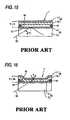
- FIGS. 15 and 16show an example of a spatial light modulator in the related art which is produced by a micromachining process including steps of film growth, photolithography, and etching of a sacrifice layer (a later which is to be removed away later in order to form a gap), and in which the light transmittance is changed by an electromechanical operation.
- a transparent electrode layer 4is stacked on an optical waveguide 3 to form a support substrate 6 , and a movable thin film 9 which is produced by the micromachining process is opposingly placed above the support substrate with being separated therefrom by a predetermined gap distance.
- the movable thin film 9is flexurally displaced by an electrostatic force acting between the support substrate 6 and the movable thin film 9 , thereby performing light modulation.
- the movable thin film 9has a stacked structure of an electrode layer 11 and an elastic layer 12 , and has given transparency.
- the gap distance between the movable thin film 9 and the support substrate 6is set by a support 14 which is interposed between the thin film 9 and the support substrate 6 .
- the movable thin film 9is enabled to be flexurally deformed toward the support substrate 6 by a gap 16 which is ensured between the thin film and the support substrate 6 by the support 14 .
- an attractive force due to an electrostatic forcedoes not act between the electrode layers 4 and 11 , and the movable thin film 9 maintains its initial flat state.
- the deviceshows optical characteristics in which incident light 18 on the optical waveguide 3 is totally reflected at the surface of the electrode layer 4 and is not emitted toward the movable thin film 9 .
- a spatial light modulator in the related art in which the returning of the movable thin film 9 to the initial state depends on the elastic restoring force of the elastic layer 12 constituting the movable thin film 9 as described abovehas a problem in that it is impossible to simultaneously realize the reduction in the operating voltage, and the increase of the ON/OFF switching speed of the spatial light modulator.
- the elastic layer 12When the elastic layer 12 is set to have a weak elastic restoring force, for example, the elastic layer 12 is easily flexurally deformed by a small electrostatic force, so that, even in the case where a low voltage is applied between the electrode layers 4 and 11 , the spatial light modulator can operates at a high speed.
- the elastic restoring forceis weak, when the applied voltage is canceled, the returning operation is slow, thereby causing a problem in that high-speed returning cannot be performed.
- the spatial light modulatorwhen the spatial light modulator is set to the ON state by applying a voltage between the electrode layers of the support substrate and the movable thin film and the voltage application is then canceled to turn OFF the spatial light modulator, the movable thin film which is deflected toward the support substrate is compulsively returned by the elastic restoring force, and also by an electrostatic attractive force which is caused to act in the direction opposite to the side of the support substrate by applying a driving voltage between the movable thin film and the returning electrode.
- the return speed of the movable thin film in the state change of the spatial light modulator from the ON state to the OFF statecan be increased even when the elastic restoring force is weak. Consequently, both the reduction in the driving voltage, and the increase of the ON/OFF switching speed of the spatial light modulator can be simultaneously realized.
- the spacerwhen the spatial light modulator is changed from the ON state to the OFF state, the spacer can prevent the movable thin film from being excessively flexurally deformed toward the returning electrode by the electrostatic force applied by the returning electrode.
- a spatial light modulatoras set forth in the first or second aspect of the invention, wherein a change of the optical characteristics is a change of total reflection conditions due to a change of a refractive index of an interface between the movable thin film and the support substrate, the refractive index change being caused by making the movable thin film contact with the support substrate.
- the interface between the support substrate and the movable thin filmis set to a light transmitting state, and, when the support substrate and the movable thin film are separated from each other, the gap between them is set to a light blocking state, thereby performing light modulation.
- a spatial light modulatoras set forth in the third aspect of the invention, wherein the electrode layer of the support substrate, the electrode layer of the movable thin film, and the returning electrode are optically transparent.
- the spatial light modulatorsince all of the electrode layer of the support substrate, that of the movable thin film, and the returning electrode are optically transparent, the reduction in the light intensity which is caused when the incident light passes through the device is suppressed so that the intensity of the emission light can be enhanced.
- a spatial light modulator arraywherein plural spatial light modulator s as set forth in any of the first to fifth aspects of the invention are arranged one- or two-dimensionally.
- the plural spatial light modulatorsare arranged one- or two-dimensionally, one- or two-dimensional light modulation can be performed.
- an image forming devicecomprising: a light source; a spatial light modulator array as set forth in the sixth aspect of the invention; an illumination optical system which illuminates the spatial light modulator array with light from the light source; and a projection optical system which projects light emitted from the spatial light modulator array onto an image forming face.
- the spatial light modulatoris illuminated with the light from the light source, and light which is modulated by the spatial light modulator array is projected by the projection optical system onto the image forming face.
- a flat panel displaycomprising: a light source which emits ultraviolet rays; a spatial light modulator array as set forth in the sixth aspect of the invention; an illumination optical system which illuminates the spatial light modulator array with light from the light source; and a fluorescent member which is excited by light emitted from the spatial light modulator array to emit light.
- the spatial light modulator arrayis illuminated with the ultraviolet rays from the light source
- the fluorescent memberis illuminated with ultraviolet rays which are emitted by a modulating operation from the spatial light modulator array
- the fluorescent memberis excited to emit display light.
- FIG. 1is a section view showing an OFF state of a spatial light modulator of a first embodiment of the invention
- FIG. 2is a section view showing an ON state of the spatial light modulator of the first embodiment of the invention
- FIG. 3is a section view showing a state change of the spatial light modulator of FIG. 2 from the ON state to the OFF state;
- FIGS. 4A and 4Bare section views showing the configuration of a spatial light modulator of a second embodiment having a spacer
- FIG. 5is a section view showing an OFF state of a spatial light modulator of a third embodiment of the invention.
- FIG. 6is a section view showing an ON state of the spatial light modulator of the third embodiment of the invention.
- FIG. 7is a section view showing a state change of the spatial light modulator of FIG. 5 from the ON state to the OFF state;
- FIG. 8is a graph showing the emission spectrum of light which is introduced into an optical waveguide of the spatial light modulator
- FIG. 9is a graph showing changes of the light transmittance of the spatial light modulator with respect to the wavelength of incident light
- FIG. 10is a view of a spatial light modulator array which is configured by arranging one- or two-dimensionally spatial light modulators
- FIG. 11is a diagram schematically showing the configuration of an exposing device which is configured by using the spatial light modulator array
- FIG. 12is a diagram schematically showing the configuration of a projecting device which is configured by using the spatial light modulator array
- FIG. 13is a diagram schematically showing the configuration of a flat panel display which is configured by using the spatial light modulator array
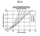
- FIG. 14is a graph showing results of simulation analyses which were conducted in order to ascertain the speed increasing effect due to the provision of a returning electrode.
- FIG. 15is a diagram schematically showing the configuration of a spatial light modulator in the related art.
- FIG. 16is a diagram illustrating the operation of the spatial light modulator in the related art.
- FIGS. 1 to 3show the configuration of the spatial light modulator of the invention.
- FIG. 1is a section view showing the OFF state of the spatial light modulator
- FIG. 2is a section view showing the ON state of the spatial light modulator
- FIG. 3is a section view showing a state change of the spatial light modulator from the ON state to the OFF state.
- the spatial light modulator 100 of the embodimentcomprises: a support substrate 6 in which a transparent electrode layer 4 is stacked on an optical waveguide 3 ; a movable thin film 9 which has a tacked structure of an electrode layer 11 and an elastic layer 12 , which is transparent, and which is placed above the support substrate 6 via a support 14 to be opposed to the support substrate with being separated by a predetermined gap distance in a manner that the film is flexurally deformable toward the support substrate 6 ; a transparent returning electrode 23 which is opposingly placed above the movable thin film 9 with being separated by a predetermined gap distance, and which causes the movable thin film 9 that is flexurally deformed toward the support substrate 6 , to be returned by an electrostatic force that is generated by an application of a voltage; and a support 25 which fixedly supports the returning electrode 23 above the movable thin film 9 .
- the term of transparentmeans transparency with respect to at least light which is to be modulated.
- the support substrate 6 , the support 14 , and the movable thin film 9are identical in configuration with those of the device in the related art shown in FIG. 15 .
- a predetermined driving voltage Vais applied between the electrode layer 4 on the support substrate 6 and the electrode layer 11 on the movable thin film 9 , therefore, the movable thin film 9 is deflected at a predetermined degree toward the support substrate 6 by the electrostatic force acting between the electrode layers as shown in FIG. 2 .
- the change of the optical characteristics due to the deflectionenables the incident light on the optical waveguide 3 to be transmitted through the movable thin film 9 .
- the spatial light modulator 100 of the embodimentis different from the spatial light modulator 1 in the related art in that the returning electrode 23 is disposed.
- the returning electrode 23will be described in detail.
- the returning electrode 23is stackingly placed on a transparent support plate 31 so as to have transparency.
- a predetermined driving voltage Vbis applied between the returning electrode 23 and the electrode layer 11 on the movable thin film 9 as shown in FIG. 3 , the returning electrode applies an electrostatic force which compulsively returns the movable thin film 9 that is flexurally displaced toward the support substrate 6 .
- the returning electrode 23allows light which has been transmitted from the support substrate 6 through the movable thin film 9 , to be transmitted therethrough to the outside.
- a metal oxide of a high electron densitysuch as ITO, a very thin metal film (such as aluminum), a thin film in which metal fine particles are dispersed in a transparent insulator, or a highly-doped wide bandgap semiconductor can be preferably used.
- the return speed of the movable thin film 9 in the state change to the OFF state of the spatial light modulatorcan be increased by the returning electrode 23 .
- both the reduction in the driving voltage, and the increase of the ON/OFF switching speed of the spatial light modulatorcan be simultaneously realized.
- the internal stress in the non-driven state in which the device is in the OFF stateis set as low as possible (for example, 20 MPa or lower), and the tensile stress state is more preferable than the compression stress state.
- the compression stress statethe movable thin film 9 is arcuately deflected, and the force of driving the device is increased. Therefore, the energy is largely lost, and the speed of the light modulation driving is lowered.
- the movable thin film 9When the stress value is a large amount, the movable thin film 9 is deflected not only toward the support substrate 6 , but also in a direction perpendicular to the deflection direction, and therefore the device is largely deformed, so that the low-voltage driving and the high-speed driving are made further difficult to perform.
- a tensile stress of the movable thin film 9is set to a small amount or lower or to a no-stress state, therefore, it is possible to form a configuration which is advantageous to the low-voltage driving and the high-speed driving.
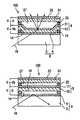
- FIGS. 4A and 4Bare section views showing the configuration of the spatial light modulator of the embodiment.
- the gap between the movable thin film 9 and the returning electrode 23is filled with a transparent spacer 27 .
- the transparent spacer 27is disposed so as to fill the gap which is formed between the movable thin film 9 and the restoring electrode 23 by the support 25 in the non-driven state of the spatial light modulator 200 .
- the spacerprevents the movable thin film from being excessively flexurally deformed toward the returning electrode 23 .
- the spacer 27useful is a material which has a predetermined insulating performance, such as silicon oxide, silicon nitride, ceramics, or a resin.
- the spacer 27can prevent the movable thin film 9 from being excessively flexurally displaced toward the returning electrode 23 .
- the placement position of the spacer 27is set so that, when the movable thin film 9 is in the initial position in the returning operation of the movable thin film 9 , the surface of the spacer 27 is in contact with that of the movable thin film 9 , and the spacer 27 is provided with an adequate buffering performance, whereby the movable thin film 9 after returning is prevented from remaining to oscillate, so that the movable thin film 9 can be rapidly stopped. As a result, the behavior of the movable thin film 9 in a high-speed operation can be stabilized.
- FIGS. 5 to 7show the configuration of the spatial light modulator of the embodiment.
- FIG. 5is a view showing the OFF state of the spatial light modulator
- FIG. 6is a view showing the ON state of the spatial light modulator
- FIG. 7is a view showing a state change of the spatial light modulator from the ON state to the OFF state.
- the spatial light modulator 300 of the embodimentcomprises: a support substrate 6 in which a transparent electrode layer 4 is stacked on a transparent substrate 13 ; a movable thin film 9 which has a stacked structure of an electrode layer 11 and an elastic layer 12 , which is transparent, and which is placed above the support substrate 6 via a support 14 to be opposed to the support substrate with being separated by a predetermined gap distance in a manner that the film is flexurally deformable toward the support substrate 6 ; a transparent returning electrode 23 which is opposingly placed above the side of the movable thin film 9 opposite to the side of the support substrate 6 , with being separated by a predetermined gap distance, and which causes the movable thin film 9 that is flexurally disposed toward the support substrate 6 , to be returned by an electrostatic force that is generated by an application of a driving voltage Vb; and a support 25 which fixedly supports the returning electrode 23 above the movable thin film 9 .
- the embodimentis identical in basic configuration with the first
- Dielectric multilayer film mirrors 43 and 45which are multilayer reflective films are disposed on the opposed surfaces of the opposed electrode layers 4 and 11 , respectively, to perform light modulation on the incident light on the principle of the Fabry-Perot modulation.
- Examples of a multilayer reflective film which performs such light modulationare a dielectric multilayer reflective film mirror, and a combination of a dielectric multilayer reflective film and a metal half mirror.
- Each of the dielectric multilayer film mirrors 43 and 45is formed by a multilayer film in which materials of different refractive indices are alternately stacked. In accordance with light to be modulated, following substances are useful as such materials.
- a material of a high refractive index(a material having a refractive index of about 1.8 or higher)
- usefulare TiO 2 , CeO 2 , Ta 2 O 5 , ZrO 2 , Sb 2 O 3 , HfO 2 , La 2 O 3 , NdO 3 , Y 2 O 3 , ZnO, and Nb 2 O 5 .
- a material of a relatively high refractive index(a material having a refractive index of about 1.6 to 1.8 or higher), useful are MgO, Al 2 O 3 , CeF 3 , LaF 3 , and NdF 3 .
- a material of a low refractive index(a material having a refractive index of about 1.5 or lower)
- usefulare SiO 2 , AlF 3 , MgF 2 , Na 3 AlF 6 , NaF, LiF, CaF 2 , and BaF 2 .
- a material of a high refractive index(a material having a refractive index of about 1.8 or higher)
- usefulare ZrO 2 , HfO 2 , La 2 O 3 , NdO 3 , Y 2 O 3 or TiO 2 , Ta 2 O 5 , and ZrO 2 (the wavelength of light is about 360 to 400 nm).
- a material of a relatively high refractive index(a material having a refractive index of about 1.6 to 1.8 or higher), useful are MgO, Al 2 O 3 , LaF 3 , and NdF 3 .
- a material of a low refractive index(a material having a refractive index of about 1.5 or lower)
- usefulare SiO 2 , AlF 3 , MgF 2 , Na 3 AlF 6 , NaF, LiF, and CaF 2 .
- the gap distance t OFF between the opposed dielectric multilayer film mirrors 43 and 45is set to a default value corresponding to the wavelength of incident light, so that light 48 which perpendicularly enters the transparent substrate 13 is reflected. Namely, the spatial light modulator is maintained to the OFF state.
- the gap distance t ON between the opposed dielectric multilayer film mirrors 43 and 45is set to a default value corresponding to the wavelength of incident light, so that light 48 which perpendicularly enters the transparent substrate 13 is transmitted through the movable thin film 9 and the returning electrode 23 .
- the spatial light modulator 300is set to the ON state.
- the spatial light modulator 300When the spatial light modulator 300 is to be switched from the ON state shown in FIG. 6 to the OFF state, the voltage application between the electrode layers 4 and 11 of the support substrate 6 and the movable thin film 9 is canceled, and the predetermined driving voltage Vb is simultaneously applied between the electrode layer 11 of the movable thin film 9 and the returning electrode 23 , thereby causing the movable thin film 9 to be returned at a higher speed from the flexural deformation.
- Vbthe predetermined driving voltage
- FIG. 8is a graph showing the emission spectrum of the light 48 incident on the support substrate 6 .
- the incident light 48is light having a center wavelength ⁇ 0 of about 360 nm.
- the wavelength of light which can be transmitted through the spatial light modulator 300is switched over.
- any combination of the gap distances t ON and t OFF , the refractive index n, the intensity reflectivities R of the dielectric multilayer film mirrors 43 and 45may be employed as far as the interference conditions are satisfied.
- the gap distance t OFF of the spatial light modulator 300 in the OFF statecan be controlled during the process of producing the device.
- the gap distance t ON of the device in the ON statecan be controlled by adjusting the balance between the electrostatic force to be generated and the elastic restoring force which is generated when the movable thin film 9 is deformed.
- the gap between the movable thin film 9 and the returning electrode 23may be filled with the above-mentioned spacer.
- FIG. 9is a graph showing light transmittances of the spatial light modulator 300 with respect to the wavelength in the case where the gap distances between the dielectric multilayer film mirrors 43 and 45 are t ON and t OFF .
- the curve Y 1shows the transmittance characteristic in the case where the gap distance between the dielectric multilayer film mirrors 43 and 45 is 270 nm. In this case, incident light having a center wavelength ⁇ 0 of 360 nm cannot be transmitted through the device.
- the curve Y 2shows the transmittance characteristic in the case where the gap distance between the dielectric multilayer film mirrors 43 and 45 is 180 nm. In this case, incident light having a center wavelength ⁇ 0 of 360 nm can be transmitted through the device.
- the incident light 48 on the transparent substrate 13has the center wavelength ⁇ 0 of about 360 nm.
- the gap distance between the dielectric multilayer film mirrors 43 and 45is t ON , therefore, the incident light can be transmitted through the spatial light modulator 300 , but, when the gap distance between the dielectric multilayer film mirrors 43 and 45 is t OFF , the incident light cannot be transmitted through the spatial light modulator 300 .
- the spatial light modulator 300when the layered structures of the dielectric multilayer film mirrors 43 and 45 are adequately changed in accordance with the wavelength of incident light, it is possible to invert the ON/OFF characteristics.
- the driving voltage Vbis applied between the electrode layer 11 and the returning electrode 23 as shown in FIG. 7 , and the returning of the movable thin film 9 can be accelerated by the electrostatic force which is exerted by the returning electrode 23 on the movable thin film 9 .
- both the reduction in the operating voltage, and the increase of the ON/OFF switching speed of the spatial light modulatorcan be simultaneously realized.
- the center wavelength of the transmission spectrumcan be arbitrarily set. According to the configuration, the amount of transmitted light can be continuously controlled. Namely, the gradation control can be performed in accordance with the applied driving voltage.
- plural spatial light modulators of any one of above-described embodimentsmay be arranged one- or two-dimensionally to constitute a spatial light modulator array 400 .
- one- or two-dimensional light modulationcan be performed.
- an image forming devicewhich is configured by using the spatial light modulator array will be described.
- an exposing device 500will be described as an example of the image forming device.
- FIG. 11is a diagram schematically showing the configuration of the exposing device which is configured by using the spatial light modulator array of the invention.
- the exposing device 500comprises: an illumination light source 61 ; an illumination optical system 62 ; a spatial light modulator array 400 in which plural spatial light modulators of any one of the above-described embodiments are arranged two-dimensionally on the same plane; and a projection optical system 64 .
- the illumination light source 61is a light source such as a laser device, a high-pressure mercury lamp, or a short arc lamp.
- the illumination optical system 62is a collimating lens which converts flat light emitted from the illumination light source 61 to parallel light.
- the parallel light which has been transmitted through the collimating lensperpendicularly enters each of the spatial light modulators of the spatial light modulator array 400 .
- the means for converting the flat light emitted from the illumination light source 61 to parallel lightknown is a method of arranging two microlenses in series, in addition to the collimating lens.
- the illumination light source 61can be deemed as a point light source, and parallel light can enter the spatial light modulator array 400 .
- parallel lightmay be caused to enter each of the spatial light modulators of the spatial light modulator array 400 by using an LED array having LEDs respectively corresponding to the spatial light modulators of the spatial light modulator array 400 as the illumination light source 61 , and causing the LED array so as to emit light while being placed near the spatial light modulator array 400 .
- the illumination optical system 62may be omitted.
- the projection optical system 64projects light onto a recording medium 65 serving as an image forming face, and is configured by, for example, a microlens array having microlenses respectively corresponding to the spatial light modulators of the spatial light modulator array 400 .
- the flat light emitted from the illumination light source 61impinges on the illumination optical system 62 .
- Light which has been converted to parallel light by the systementers the spatial light modulator array 400 .
- the transmittanceis controlled in accordance with an image signal.
- Light emitted from the spatial light modulator array 400is projected by the projection optical system 64 onto the image forming face of the recording medium 65 .
- the projection lightis projected onto the recording medium 65 while being relatively moved in a scanning direction, so that a large area can be exposed at a high resolution.
- the spatial light modulator array 400may be an array in which plural spatial light modulators of the third embodiment are one-dimensionally arranged on the same plane.
- an optical element which selects an optical pathis placed across a transparent medium on the light entering side of each of the spatial light modulators.
- the transparent mediumthe optical waveguide 3 may be used as it is.
- a layer of a transparent mediummay be formed between the optical waveguide 3 and the electrode layer 4 .
- the optical element which selects an optical pathmeans an optical element in which a substantially whole of selected transmission light emitted from the optical element has an angular component that is larger than the critical angle of total reflection in the front layer in the optical path of incident light, and incident light having another angular component is selectively reflected so as not to be transmitted through the optical element.
- incident light having another angular componentis selectively reflected so as not to be transmitted through the optical element.
- optical element which selects an optical pathis an optical interference filter formed by a dielectric multilayer film.
- cholesteric liquid crystal devicefunctioning as a Bragg reflection filter may be used.
- a microlens arraymay be used as the illumination optical system 62 .
- the deviceis designed and adjusted sot that the microlenses of the microlens array correspond to the spatial light modulators of the spatial light modulator array 400 , respectively, and the axis and focal plane of each microlens coincide with the center of the corresponding spatial light modulator.
- the incident light from the illumination light source 61is converged by the microlens array into respective regions which are smaller in area than each of the spatial light modulators, and then enters the spatial light modulator array 400 .
- the transmittanceis controlled by a control device (not shown) in accordance with the image signal.
- Light emitted from the spatial light modulator array 400is projected by the projection optical system 64 onto the image forming face of the recording medium 65 .
- the projection lightis projected onto the recording medium 65 while being relatively moved in a scanning direction, so that a large area can be exposed at a high resolution.
- the light from the illumination light source 61can be converged by the microlens array, and hence it is possible to realize an exposing device having an improved light utilization efficiency.
- each microlensis not particularly limited and may be spherical or semispherical, or have a convex curved surface or a concave curved surface.
- the microlens arraymay be formed into a flat shape having a refractive index distribution, or may be configured by arraying Fresnel lenses or diffraction lenses due to binary optics or the like.
- Examples of the material of the microlensesare transparent glass and a resin. From the viewpoint of the mass productivity, a resin is superior, and, from the viewpoint of the life period and the reliability, glass is superior. From an optical viewpoint, as the glass, quartz glass, fused silica glass, alkali-free glass, and the like are preferable, and, as the resin, an acrylic resin, an epoxy resin, a polyester resin, a polycarbonate resin, a styrene resin, a vinyl chloride resin, and the like are preferable.
- the resinmay be of the photo curing type, the thermoplastic type, or the like. It is preferable to adequately select the type of the resin in accordance with the method of producing the microlenses.
- a practical method of producing the microlensesis a method such as the cast molding method using dies, the press molding method, the injection molding method, the printing method, or the photolithography method.
- the cast molding methodin which a photo (ultraviolet rays or the like) curing resin, or the photolithography method in which a positive or negative resist material is used is preferably used, and, in the case where the microlenses are to be formed by glass, the resist transfer method using RIE (reactive ion etching), the isotropic etching method, or the ion exchange method is preferably used.
- microlensesare to be formed by the die molding method
- a thermoplastic resinis hot pressed by dies having a shape identical with that of the microlenses.
- the molding processis preferably conducted in the following manner. A photo curing resin or a thermoplastic resin is filled into dies and then pressed, the resin is thereafter cured by light or heat, and the cured resin is separated from the dies. According to the method, fine molding is enabled.
- a photo curing resinwhich is less expanded and contracted by heat.
- microlenses made of a resinare to be formed by the photolithography method
- a photo-dissolving resinwhich is typified by a transparent photoresist or a photo-curing resin is exposed by ultraviolet rays (or visible rays) through an adequately patterned light shielding mask, and exposed portions or unexposed portions are dissolved and developed to form microlenses.
- ultraviolet raysor visible rays
- a baking processmay be conducted after developing, and microlenses of a desired shape may be obtained by means of the surface tension when the resin material is thermally softened (the reflow method).
- the microlensesare formed by etching a transparent substrate on which spatial light modulators are configured, and through which light from the above-mentioned light source can be transmitted.
- the etching processwhen a film is applied in a shape corresponding to the microlenses, the substrate can be easily processed into the desired shape.
- FIG. 12is a diagram schematically showing the configuration of a projecting device which is configured by using the spatial light modulator array of the invention.
- the components identical with those of FIG. 11are denoted by the same reference numerals, and their description is omitted.
- a projector 600 serving as a projecting devicecomprises an illumination light source 61 ; an illumination optical system 62 ; a spatial light modulator array 400 ; and a projection optical system 74 .
- the projection optical system 74is an optical system for the projecting device which projects light onto a screen 75 functioning as an image forming face.
- the incident light from the illumination light source 61is converged by the microlens array into respective regions which are smaller in area than each of the spatial light modulators, and then enters the spatial light modulator array 400 .
- the transmittanceis controlled in accordance with the image signal.
- Light emitted from the spatial light modulator array 400is projected by the projection optical system 74 onto the image forming face of the screen 75 .
- the spatial light modulator array 400can be used also in a projecting device. Furthermore, the spatial light modulator array 400 can be applied also to a display device.
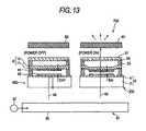
- a display device 700comprises: a spatial light modulator array 450 in which plural spatial light modulators 300 described above are arranged one- or two-dimensionally; a light source unit 81 which is disposed on the light incident side of the spatial light modulator array 450 , and which emits ultraviolet rays; and fluorescent members 83 which are disposed on the light emission side of the spatial light modulator array 450 , and which receive light emitted from the respective spatial light modulators 300 to be excited thereby to emit light.
- the fluorescent members 83emit the three primary colors (such as red, blue, and green, or cyan, magenta, and yellow), and are arranged in adequate sequence, thereby enabling the display device to provide a full-color display.
- the light source unit 81has: a waveguide 85 for producing flat light; and a black light ultraviolet lamp (low-pressure mercury lamp) 87 which is placed on a side face of the waveguide 85 .
- the waveguide 85functioning as an illumination optical system receives ultraviolet rays from the black light low-pressure mercury lamp 87 serving as a light source, through the side face, and emits the light as the incident light 48 from the surface opposed to the spatial light modulator 300 .
- the emitted ultraviolet raysWhen a fluorescent material for black light (such as BaSi 2 O 5 :Pb 2+ ) is applied to the inner wall of the low-pressure mercury lamp 87 , the emitted ultraviolet rays have the spectral characteristics of FIG. 8 , or have a center wavelength ⁇ 0 in the vicinity of 360 nm.
- the ultraviolet raysare used as a back light.
- the movable thin film 9is deflected toward the support substrate 6 , whereby a multilayer film interference effect is produced so that light modulation can be performed on the ultraviolet rays.
- the driving voltage between the electrode layers 4 and 11is turned OFF and a driving voltage is applied between the electrode layer 11 and the returning electrode 23 , the movable thin film 9 can be returned at a high speed from the flexural deformation. As a result, an image display of high responsibility is enabled, and an excellent performance of displaying a moving picture can be obtained.
- the display devicemay be configured so that the incident light to be guided to the spatial light modulator array 450 of the flat panel display 700 is obtained by converging the light from the light source by a microlens array.
- the incident lightcan be concentrated only to the light modulation region (the region of the dielectric multilayer film mirrors 43 and 45 ) of each spatial light modulator, so that the incident light can be prevented from being wastefully absorbed by a region other than the light modulation region. Therefore, the light utilization efficiency can be improved, and the display brightness can be increased.
- the driving voltageis applied between the electrode layers 4 and 11 , and an attractive force due to an electrostatic force is caused to act between the electrode layers 4 and 11 , whereby the movable thin film 9 is downward displaced.
- the voltage applied between the electrode layers 4 and 11is turned OFF, and the movable thin film 9 is returned by its elastic restoring force.
- the driving voltageis applied between the electrode layer 4 of the support substrate 6 and the electrode layer 11 of the movable thin film 9 , and the movable thin film is downward displaced by an attractive force acting between the electrode layers 4 and 11 .
- the voltage applied between the electrode layers 4 and 11is turned OFF, and the driving voltage is applied between the electrode layer 11 of the movable thin film 9 and the returning electrode 23 on the support plate 31 , so that the movable thin film 9 is returned by its elastic restoring force and the attractive force.
- the function of the returning electrode 23causes the force of returning the movable thin film 9 to be larger by the degree corresponding to the attractive force due to the electrostatic force than that in the conventional spatial light modulator 1 shown in FIG. 15 .
- the speed of the returning operationis increased.
- FIG. 14shows results of the analyses.
- the driving voltageis applied between the electrode layers 4 and 11 to set the state where the movable thin film 9 is displaced toward the support substrate 6 and the gap 16 is not formed.
- the value of the displacement distance of the movable thin film 9is at a position (point A of FIG. 14 ) below 0.23 ⁇ m.
- the response characteristics at each driving voltagewas analyzed.
- the response timemeans the time required for the movable thin film 9 to return from the displaced state (point A) to the state (point B of FIG. 14 ) before the displacement.
- the results at the driving voltage of 0 Vcorrespond to the return time in a device which configured in the same manner as the conventional device.
- the return timeis shorter as compared with that at the driving voltage of 0 V.
- the return time when the driving voltage is 0 Vis about 0.225 ⁇ s
- that when the driving voltage is 20 Vis about 0.115 ⁇ s.
- the speedis increased by about two times.
- resultswere obtained by raising the driving voltage to 20 V. It is supposed that the speed can be made faster by further raising the voltage. As a result, it has been found that a spatial light modulator can be driven at a higher speed by disposing a returning electrode.
- the spatial light modulatorwhen the spatial light modulator is set to the ON state by applying a voltage between the electrode layers of the support substrate and the movable thin film and the voltage application is then canceled to turn OFF the spatial light modulator, the movable thin film which is deflected toward the support substrate is compulsively returned by the elastic restoring force, and also by an electrostatic attractive force which is caused to act in the direction opposite to the side of the support substrate by applying a driving voltage between the movable thin film and the returning electrode.
- the return speed of the movable thin film in the state change of the spatial light modulator from the ON state to the OFF statecan be increased even when the elastic restoring force is weak. Consequently, both the reduction in the driving voltage, and the increase of the ON/OFF switching speed of the spatial light modulator can be simultaneously realized.
Landscapes
- Physics & Mathematics (AREA)
- General Physics & Mathematics (AREA)
- Optics & Photonics (AREA)
- Spectroscopy & Molecular Physics (AREA)
- Mechanical Light Control Or Optical Switches (AREA)
Abstract
Description
tON=½×λ0=180 nm
tOFF= 3/3×λ0=270 nm.
θc=sin−1(n2/n1).
- material: Al thickness: t=0.15 μm
- material: Al thickness: t=0.4 μm
- material: Al thickness: t=0.15 μm
- material: SiN thickness: t=0.8 μm
Claims (11)
Applications Claiming Priority (2)
| Application Number | Priority Date | Filing Date | Title |
|---|---|---|---|
| JPP.2003-009808 | 2003-01-17 | ||
| JP2003009808 | 2003-01-17 |
Publications (2)
| Publication Number | Publication Date |
|---|---|
| US20040222418A1 US20040222418A1 (en) | 2004-11-11 |
| US6930816B2true US6930816B2 (en) | 2005-08-16 |
Family
ID=33398230
Family Applications (1)
| Application Number | Title | Priority Date | Filing Date |
|---|---|---|---|
| US10/758,278Expired - Fee RelatedUS6930816B2 (en) | 2003-01-17 | 2004-01-16 | Spatial light modulator, spatial light modulator array, image forming device and flat panel display |
Country Status (1)
| Country | Link |
|---|---|
| US (1) | US6930816B2 (en) |
Cited By (64)
| Publication number | Priority date | Publication date | Assignee | Title |
|---|---|---|---|---|
| US20050064116A1 (en)* | 2003-09-23 | 2005-03-24 | Yi-An Sha | Polymer gel display, fabrication method and operating structure thereof |
| US20050195461A1 (en)* | 2004-01-26 | 2005-09-08 | Fuji Photo Film Co., Ltd. | Spatial light modulator, spatial light modulator array, and image formation apparatus |
| US20050202649A1 (en)* | 2004-03-10 | 2005-09-15 | Po-Chung Hung | Optical interference reflective element and repairing and manufacturing methods thereof |
| US20060066641A1 (en)* | 2004-09-27 | 2006-03-30 | Gally Brian J | Method and device for manipulating color in a display |
| US20060077124A1 (en)* | 2004-09-27 | 2006-04-13 | Gally Brian J | Method and device for manipulating color in a display |
| US20060077154A1 (en)* | 2004-09-27 | 2006-04-13 | Gally Brian J | Optical films for directing light towards active areas of displays |
| US20060077125A1 (en)* | 2004-09-27 | 2006-04-13 | Idc, Llc. A Delaware Limited Liability Company | Method and device for generating white in an interferometric modulator display |
| US20060077509A1 (en)* | 2004-09-27 | 2006-04-13 | Ming-Hau Tung | Method and post structures for interferometric modulation |
| US20070171531A1 (en)* | 2006-01-19 | 2007-07-26 | Seiko Epson Corporation | Optical device |
| WO2007127046A3 (en)* | 2006-04-21 | 2007-12-27 | Qualcomm Inc | Method and apparatus for providing brightness control in an interferometric modulator (imod) display |
| US20070297191A1 (en)* | 2006-06-21 | 2007-12-27 | Sampsell Jeffrey B | Linear solid state illuminator |
| US7349139B2 (en) | 2004-09-27 | 2008-03-25 | Idc, Llc | System and method of illuminating interferometric modulators using backlighting |
| US20080218834A1 (en)* | 2007-03-08 | 2008-09-11 | Qualcomm Mems Technologies, Inc. | Method and apparatus for providing a light absorbing mask in an interferometric modulator display |
| US7463421B2 (en) | 1994-05-05 | 2008-12-09 | Idc, Llc | Method and device for modulating light |
| US7483197B2 (en) | 1999-10-05 | 2009-01-27 | Idc, Llc | Photonic MEMS and structures |
| US7515325B2 (en) | 2006-01-19 | 2009-04-07 | Seiko Epson Corporation | Optical device |
| US7603001B2 (en) | 2006-02-17 | 2009-10-13 | Qualcomm Mems Technologies, Inc. | Method and apparatus for providing back-lighting in an interferometric modulator display device |
| US20090284985A1 (en)* | 2008-05-16 | 2009-11-19 | Qualcomm Mems Technologies, Inc. | Illumination apparatus and methods |
| US20090303746A1 (en)* | 2008-06-04 | 2009-12-10 | Qualcomm Mems Technologies, Inc. | Edge shadow reducing methods for prismatic front light |
| US7649671B2 (en)* | 2006-06-01 | 2010-01-19 | Qualcomm Mems Technologies, Inc. | Analog interferometric modulator device with electrostatic actuation and release |
| US7706050B2 (en) | 2004-03-05 | 2010-04-27 | Qualcomm Mems Technologies, Inc. | Integrated modulator illumination |
| US7710632B2 (en) | 2004-09-27 | 2010-05-04 | Qualcomm Mems Technologies, Inc. | Display device having an array of spatial light modulators with integrated color filters |
| US7733439B2 (en) | 2007-04-30 | 2010-06-08 | Qualcomm Mems Technologies, Inc. | Dual film light guide for illuminating displays |
| US20100165443A1 (en)* | 2004-09-27 | 2010-07-01 | Qualcomm Mems Technologies, Inc. | Systems and methods using interferometric optical modulators and diffusers |
| US7750886B2 (en) | 2004-09-27 | 2010-07-06 | Qualcomm Mems Technologies, Inc. | Methods and devices for lighting displays |
| US7777954B2 (en) | 2007-01-30 | 2010-08-17 | Qualcomm Mems Technologies, Inc. | Systems and methods of providing a light guiding layer |
| US7807488B2 (en) | 2004-09-27 | 2010-10-05 | Qualcomm Mems Technologies, Inc. | Display element having filter material diffused in a substrate of the display element |
| US7813026B2 (en) | 2004-09-27 | 2010-10-12 | Qualcomm Mems Technologies, Inc. | System and method of reducing color shift in a display |
| US7845841B2 (en) | 2006-08-28 | 2010-12-07 | Qualcomm Mems Technologies, Inc. | Angle sweeping holographic illuminator |
| US7855827B2 (en) | 2006-10-06 | 2010-12-21 | Qualcomm Mems Technologies, Inc. | Internal optical isolation structure for integrated front or back lighting |
| US7855824B2 (en) | 2004-03-06 | 2010-12-21 | Qualcomm Mems Technologies, Inc. | Method and system for color optimization in a display |
| US7864395B2 (en) | 2006-10-27 | 2011-01-04 | Qualcomm Mems Technologies, Inc. | Light guide including optical scattering elements and a method of manufacture |
| US20110025727A1 (en)* | 2009-08-03 | 2011-02-03 | Qualcomm Mems Technologies, Inc. | Microstructures for light guide illumination |
| US7898521B2 (en) | 2004-09-27 | 2011-03-01 | Qualcomm Mems Technologies, Inc. | Device and method for wavelength filtering |
| US7911428B2 (en) | 2004-09-27 | 2011-03-22 | Qualcomm Mems Technologies, Inc. | Method and device for manipulating color in a display |
| US7928928B2 (en) | 2004-09-27 | 2011-04-19 | Qualcomm Mems Technologies, Inc. | Apparatus and method for reducing perceived color shift |
| US7949213B2 (en) | 2007-12-07 | 2011-05-24 | Qualcomm Mems Technologies, Inc. | Light illumination of displays with front light guide and coupling elements |
| US8023167B2 (en)* | 2008-06-25 | 2011-09-20 | Qualcomm Mems Technologies, Inc. | Backlight displays |
| US8040589B2 (en) | 2008-02-12 | 2011-10-18 | Qualcomm Mems Technologies, Inc. | Devices and methods for enhancing brightness of displays using angle conversion layers |
| US8045252B2 (en) | 2004-02-03 | 2011-10-25 | Qualcomm Mems Technologies, Inc. | Spatial light modulator with integrated optical compensation structure |
| US8049951B2 (en) | 2008-04-15 | 2011-11-01 | Qualcomm Mems Technologies, Inc. | Light with bi-directional propagation |
| US8061882B2 (en) | 2006-10-06 | 2011-11-22 | Qualcomm Mems Technologies, Inc. | Illumination device with built-in light coupler |
| US8068710B2 (en) | 2007-12-07 | 2011-11-29 | Qualcomm Mems Technologies, Inc. | Decoupled holographic film and diffuser |
| US8107155B2 (en) | 2006-10-06 | 2012-01-31 | Qualcomm Mems Technologies, Inc. | System and method for reducing visual artifacts in displays |
| US8172417B2 (en) | 2009-03-06 | 2012-05-08 | Qualcomm Mems Technologies, Inc. | Shaped frontlight reflector for use with display |
| US8193441B2 (en) | 2007-12-17 | 2012-06-05 | Qualcomm Mems Technologies, Inc. | Photovoltaics with interferometric ribbon masks |
| US20120140134A1 (en)* | 2009-06-05 | 2012-06-07 | Heon Young Lee | Display panel using flexibility of metal thin film patterns and fabricating method thereof |
| US8300304B2 (en) | 2008-02-12 | 2012-10-30 | Qualcomm Mems Technologies, Inc. | Integrated front light diffuser for reflective displays |
| US20120287519A1 (en)* | 2011-05-10 | 2012-11-15 | National Taiwan University | Optical system, optical module and method of manufacture thereof |
| US8346048B2 (en) | 2008-05-28 | 2013-01-01 | Qualcomm Mems Technologies, Inc. | Front light devices and methods of fabrication thereof |
| US8362987B2 (en) | 2004-09-27 | 2013-01-29 | Qualcomm Mems Technologies, Inc. | Method and device for manipulating color in a display |
| US8368981B2 (en) | 2006-10-10 | 2013-02-05 | Qualcomm Mems Technologies, Inc. | Display device with diffractive optics |
| US8654061B2 (en) | 2008-02-12 | 2014-02-18 | Qualcomm Mems Technologies, Inc. | Integrated front light solution |
| US8670171B2 (en) | 2010-10-18 | 2014-03-11 | Qualcomm Mems Technologies, Inc. | Display having an embedded microlens array |
| US8693084B2 (en) | 2008-03-07 | 2014-04-08 | Qualcomm Mems Technologies, Inc. | Interferometric modulator in transmission mode |
| US8848294B2 (en) | 2010-05-20 | 2014-09-30 | Qualcomm Mems Technologies, Inc. | Method and structure capable of changing color saturation |
| US8872085B2 (en) | 2006-10-06 | 2014-10-28 | Qualcomm Mems Technologies, Inc. | Display device having front illuminator with turning features |
| US8902484B2 (en) | 2010-12-15 | 2014-12-02 | Qualcomm Mems Technologies, Inc. | Holographic brightness enhancement film |
| US8928967B2 (en) | 1998-04-08 | 2015-01-06 | Qualcomm Mems Technologies, Inc. | Method and device for modulating light |
| US8971675B2 (en) | 2006-01-13 | 2015-03-03 | Qualcomm Mems Technologies, Inc. | Interconnect structure for MEMS device |
| US8979349B2 (en) | 2009-05-29 | 2015-03-17 | Qualcomm Mems Technologies, Inc. | Illumination devices and methods of fabrication thereof |
| US9019183B2 (en) | 2006-10-06 | 2015-04-28 | Qualcomm Mems Technologies, Inc. | Optical loss structure integrated in an illumination apparatus |
| US9025235B2 (en) | 2002-12-25 | 2015-05-05 | Qualcomm Mems Technologies, Inc. | Optical interference type of color display having optical diffusion layer between substrate and electrode |
| US9110289B2 (en) | 1998-04-08 | 2015-08-18 | Qualcomm Mems Technologies, Inc. | Device for modulating light with multiple electrodes |
Families Citing this family (11)
| Publication number | Priority date | Publication date | Assignee | Title |
|---|---|---|---|---|
| US20050195370A1 (en)* | 2004-03-02 | 2005-09-08 | Gore Makarand P. | Transmissive/reflective light engine |
| US7267442B2 (en)* | 2004-10-20 | 2007-09-11 | Hewlett-Packard Development Company, L.P. | Pixelated color wobulation |
| US7760412B2 (en)* | 2005-03-08 | 2010-07-20 | University Of Delaware | Mechanically-active anti-reflection switch (MARS) modulator with wide angle tolerance |
| US7548302B2 (en)* | 2005-03-29 | 2009-06-16 | Asml Netherlands B.V. | Lithographic apparatus and device manufacturing method |
| US7317506B2 (en)* | 2005-03-29 | 2008-01-08 | Asml Netherlands B.V. | Variable illumination source |
| KR20100084518A (en)* | 2007-09-17 | 2010-07-26 | 퀄컴 엠이엠스 테크놀로지스, 인크. | Semi-transparent/transflective lighted interferometric modulator devices |
| US7957049B1 (en)* | 2010-02-12 | 2011-06-07 | Sharp Kabushiki Kaisha | Highly reflective MEMS device |
| US20140036343A1 (en)* | 2012-07-31 | 2014-02-06 | Qualcomm Mems Technologies, Inc. | Interferometric modulator with improved primary colors |
| CN107768362B (en) | 2013-03-28 | 2020-09-08 | 东芝北斗电子株式会社 | Light emitting device and method for manufacturing the same |
| US10359551B2 (en)* | 2013-08-12 | 2019-07-23 | Axsun Technologies, Inc. | Dielectric-enhanced metal coatings for MEMS tunable filters |
| WO2016176735A1 (en) | 2015-05-05 | 2016-11-10 | University Of Western Australia | Microelectromechanical systems (mems) and methods |
Citations (3)
| Publication number | Priority date | Publication date | Assignee | Title |
|---|---|---|---|---|
| JPH11258558A (en) | 1998-03-13 | 1999-09-24 | Fuji Photo Film Co Ltd | Flat panel display |
| JP2000214804A (en) | 1999-01-20 | 2000-08-04 | Fuji Photo Film Co Ltd | Light modulation element, aligner, and planar display |
| US6195196B1 (en)* | 1998-03-13 | 2001-02-27 | Fuji Photo Film Co., Ltd. | Array-type exposing device and flat type display incorporating light modulator and driving method thereof |
- 2004
- 2004-01-16USUS10/758,278patent/US6930816B2/ennot_activeExpired - Fee Related
Patent Citations (4)
| Publication number | Priority date | Publication date | Assignee | Title |
|---|---|---|---|---|
| JPH11258558A (en) | 1998-03-13 | 1999-09-24 | Fuji Photo Film Co Ltd | Flat panel display |
| US6195196B1 (en)* | 1998-03-13 | 2001-02-27 | Fuji Photo Film Co., Ltd. | Array-type exposing device and flat type display incorporating light modulator and driving method thereof |
| JP2000214804A (en) | 1999-01-20 | 2000-08-04 | Fuji Photo Film Co Ltd | Light modulation element, aligner, and planar display |
| US6642913B1 (en)* | 1999-01-20 | 2003-11-04 | Fuji Photo Film Co., Ltd. | Light modulation element, exposure unit, and flat-panel display unit |
Cited By (94)
| Publication number | Priority date | Publication date | Assignee | Title |
|---|---|---|---|---|
| US8059326B2 (en) | 1994-05-05 | 2011-11-15 | Qualcomm Mems Technologies Inc. | Display devices comprising of interferometric modulator and sensor |
| US7463421B2 (en) | 1994-05-05 | 2008-12-09 | Idc, Llc | Method and device for modulating light |
| US8928967B2 (en) | 1998-04-08 | 2015-01-06 | Qualcomm Mems Technologies, Inc. | Method and device for modulating light |
| US9110289B2 (en) | 1998-04-08 | 2015-08-18 | Qualcomm Mems Technologies, Inc. | Device for modulating light with multiple electrodes |
| US7483197B2 (en) | 1999-10-05 | 2009-01-27 | Idc, Llc | Photonic MEMS and structures |
| US9025235B2 (en) | 2002-12-25 | 2015-05-05 | Qualcomm Mems Technologies, Inc. | Optical interference type of color display having optical diffusion layer between substrate and electrode |
| US20050064116A1 (en)* | 2003-09-23 | 2005-03-24 | Yi-An Sha | Polymer gel display, fabrication method and operating structure thereof |
| US7027206B2 (en)* | 2004-01-26 | 2006-04-11 | Fuji Photo Film Co., Ltd. | Spatial light modulator, spatial light modulator array, and image formation apparatus |
| US20050195461A1 (en)* | 2004-01-26 | 2005-09-08 | Fuji Photo Film Co., Ltd. | Spatial light modulator, spatial light modulator array, and image formation apparatus |
| US8045252B2 (en) | 2004-02-03 | 2011-10-25 | Qualcomm Mems Technologies, Inc. | Spatial light modulator with integrated optical compensation structure |
| US8111445B2 (en) | 2004-02-03 | 2012-02-07 | Qualcomm Mems Technologies, Inc. | Spatial light modulator with integrated optical compensation structure |
| US9019590B2 (en) | 2004-02-03 | 2015-04-28 | Qualcomm Mems Technologies, Inc. | Spatial light modulator with integrated optical compensation structure |
| US7706050B2 (en) | 2004-03-05 | 2010-04-27 | Qualcomm Mems Technologies, Inc. | Integrated modulator illumination |
| US7880954B2 (en) | 2004-03-05 | 2011-02-01 | Qualcomm Mems Technologies, Inc. | Integrated modulator illumination |
| US7855824B2 (en) | 2004-03-06 | 2010-12-21 | Qualcomm Mems Technologies, Inc. | Method and system for color optimization in a display |
| US6980350B2 (en)* | 2004-03-10 | 2005-12-27 | Prime View International Co., Ltd. | Optical interference reflective element and repairing and manufacturing methods thereof |
| US20050202649A1 (en)* | 2004-03-10 | 2005-09-15 | Po-Chung Hung | Optical interference reflective element and repairing and manufacturing methods thereof |
| US7807488B2 (en) | 2004-09-27 | 2010-10-05 | Qualcomm Mems Technologies, Inc. | Display element having filter material diffused in a substrate of the display element |
| US20100165443A1 (en)* | 2004-09-27 | 2010-07-01 | Qualcomm Mems Technologies, Inc. | Systems and methods using interferometric optical modulators and diffusers |
| US7928928B2 (en) | 2004-09-27 | 2011-04-19 | Qualcomm Mems Technologies, Inc. | Apparatus and method for reducing perceived color shift |
| US7525730B2 (en) | 2004-09-27 | 2009-04-28 | Idc, Llc | Method and device for generating white in an interferometric modulator display |
| US20110193770A1 (en)* | 2004-09-27 | 2011-08-11 | Qualcomm Mems Technologies, Inc. | Device and method for wavelength filtering |
| US7561323B2 (en) | 2004-09-27 | 2009-07-14 | Idc, Llc | Optical films for directing light towards active areas of displays |
| US7349139B2 (en) | 2004-09-27 | 2008-03-25 | Idc, Llc | System and method of illuminating interferometric modulators using backlighting |
| US7911428B2 (en) | 2004-09-27 | 2011-03-22 | Qualcomm Mems Technologies, Inc. | Method and device for manipulating color in a display |
| US20090296191A1 (en)* | 2004-09-27 | 2009-12-03 | Idc, Llc | Method and device for generating white in an interferometric modulator display |
| US7349141B2 (en)* | 2004-09-27 | 2008-03-25 | Idc, Llc | Method and post structures for interferometric modulation |
| US8416154B2 (en) | 2004-09-27 | 2013-04-09 | Qualcomm Mems Technologies, Inc. | Apparatus and method for reducing perceived color shift |
| US7898521B2 (en) | 2004-09-27 | 2011-03-01 | Qualcomm Mems Technologies, Inc. | Device and method for wavelength filtering |
| US7710632B2 (en) | 2004-09-27 | 2010-05-04 | Qualcomm Mems Technologies, Inc. | Display device having an array of spatial light modulators with integrated color filters |
| US7719747B2 (en) | 2004-09-27 | 2010-05-18 | Qualcomm Mems Technologies, Inc. | Method and post structures for interferometric modulation |
| US8362987B2 (en) | 2004-09-27 | 2013-01-29 | Qualcomm Mems Technologies, Inc. | Method and device for manipulating color in a display |
| US7355780B2 (en) | 2004-09-27 | 2008-04-08 | Idc, Llc | System and method of illuminating interferometric modulators using backlighting |
| US7750886B2 (en) | 2004-09-27 | 2010-07-06 | Qualcomm Mems Technologies, Inc. | Methods and devices for lighting displays |
| US20060077509A1 (en)* | 2004-09-27 | 2006-04-13 | Ming-Hau Tung | Method and post structures for interferometric modulation |
| US8102407B2 (en) | 2004-09-27 | 2012-01-24 | Qualcomm Mems Technologies, Inc. | Method and device for manipulating color in a display |
| US7944602B2 (en) | 2004-09-27 | 2011-05-17 | Qualcomm Mems Technologies, Inc. | Systems and methods using interferometric optical modulators and diffusers |
| US7813026B2 (en) | 2004-09-27 | 2010-10-12 | Qualcomm Mems Technologies, Inc. | System and method of reducing color shift in a display |
| US8098431B2 (en) | 2004-09-27 | 2012-01-17 | Qualcomm Mems Technologies, Inc. | Method and device for generating white in an interferometric modulator display |
| US20060077125A1 (en)* | 2004-09-27 | 2006-04-13 | Idc, Llc. A Delaware Limited Liability Company | Method and device for generating white in an interferometric modulator display |
| US20060077154A1 (en)* | 2004-09-27 | 2006-04-13 | Gally Brian J | Optical films for directing light towards active areas of displays |
| US20060077124A1 (en)* | 2004-09-27 | 2006-04-13 | Gally Brian J | Method and device for manipulating color in a display |
| US20060066641A1 (en)* | 2004-09-27 | 2006-03-30 | Gally Brian J | Method and device for manipulating color in a display |
| US8040588B2 (en) | 2004-09-27 | 2011-10-18 | Qualcomm Mems Technologies, Inc. | System and method of illuminating interferometric modulators using backlighting |
| US8031133B2 (en) | 2004-09-27 | 2011-10-04 | Qualcomm Mems Technologies, Inc. | Method and device for manipulating color in a display |
| US8971675B2 (en) | 2006-01-13 | 2015-03-03 | Qualcomm Mems Technologies, Inc. | Interconnect structure for MEMS device |
| US20070171531A1 (en)* | 2006-01-19 | 2007-07-26 | Seiko Epson Corporation | Optical device |
| US7525713B2 (en) | 2006-01-19 | 2009-04-28 | Seiko Epson Corporation | Optical device |
| US7515325B2 (en) | 2006-01-19 | 2009-04-07 | Seiko Epson Corporation | Optical device |
| US7603001B2 (en) | 2006-02-17 | 2009-10-13 | Qualcomm Mems Technologies, Inc. | Method and apparatus for providing back-lighting in an interferometric modulator display device |
| US8077380B2 (en)* | 2006-04-21 | 2011-12-13 | Qualcomm Mems Technologies, Inc. | Method and apparatus for providing brightness control in an interferometric modulator (IMOD) display |
| US8004743B2 (en)* | 2006-04-21 | 2011-08-23 | Qualcomm Mems Technologies, Inc. | Method and apparatus for providing brightness control in an interferometric modulator (IMOD) display |
| WO2007127046A3 (en)* | 2006-04-21 | 2007-12-27 | Qualcomm Inc | Method and apparatus for providing brightness control in an interferometric modulator (imod) display |
| US20110043889A1 (en)* | 2006-04-21 | 2011-02-24 | Qualcomm Mems Technologies, Inc. | Method and apparatus for providing brightness control in an interferometric modulator (imod) display |
| US7649671B2 (en)* | 2006-06-01 | 2010-01-19 | Qualcomm Mems Technologies, Inc. | Analog interferometric modulator device with electrostatic actuation and release |
| US8098416B2 (en) | 2006-06-01 | 2012-01-17 | Qualcomm Mems Technologies, Inc. | Analog interferometric modulator device with electrostatic actuation and release |
| US20070297191A1 (en)* | 2006-06-21 | 2007-12-27 | Sampsell Jeffrey B | Linear solid state illuminator |
| US7766498B2 (en) | 2006-06-21 | 2010-08-03 | Qualcomm Mems Technologies, Inc. | Linear solid state illuminator |
| US7845841B2 (en) | 2006-08-28 | 2010-12-07 | Qualcomm Mems Technologies, Inc. | Angle sweeping holographic illuminator |
| US8061882B2 (en) | 2006-10-06 | 2011-11-22 | Qualcomm Mems Technologies, Inc. | Illumination device with built-in light coupler |
| US8872085B2 (en) | 2006-10-06 | 2014-10-28 | Qualcomm Mems Technologies, Inc. | Display device having front illuminator with turning features |
| US7855827B2 (en) | 2006-10-06 | 2010-12-21 | Qualcomm Mems Technologies, Inc. | Internal optical isolation structure for integrated front or back lighting |
| US9019183B2 (en) | 2006-10-06 | 2015-04-28 | Qualcomm Mems Technologies, Inc. | Optical loss structure integrated in an illumination apparatus |
| US8107155B2 (en) | 2006-10-06 | 2012-01-31 | Qualcomm Mems Technologies, Inc. | System and method for reducing visual artifacts in displays |
| US8368981B2 (en) | 2006-10-10 | 2013-02-05 | Qualcomm Mems Technologies, Inc. | Display device with diffractive optics |
| US7864395B2 (en) | 2006-10-27 | 2011-01-04 | Qualcomm Mems Technologies, Inc. | Light guide including optical scattering elements and a method of manufacture |
| US7777954B2 (en) | 2007-01-30 | 2010-08-17 | Qualcomm Mems Technologies, Inc. | Systems and methods of providing a light guiding layer |
| US20080218834A1 (en)* | 2007-03-08 | 2008-09-11 | Qualcomm Mems Technologies, Inc. | Method and apparatus for providing a light absorbing mask in an interferometric modulator display |
| US7916378B2 (en) | 2007-03-08 | 2011-03-29 | Qualcomm Mems Technologies, Inc. | Method and apparatus for providing a light absorbing mask in an interferometric modulator display |
| US7733439B2 (en) | 2007-04-30 | 2010-06-08 | Qualcomm Mems Technologies, Inc. | Dual film light guide for illuminating displays |
| US8068710B2 (en) | 2007-12-07 | 2011-11-29 | Qualcomm Mems Technologies, Inc. | Decoupled holographic film and diffuser |
| US7949213B2 (en) | 2007-12-07 | 2011-05-24 | Qualcomm Mems Technologies, Inc. | Light illumination of displays with front light guide and coupling elements |
| US8798425B2 (en) | 2007-12-07 | 2014-08-05 | Qualcomm Mems Technologies, Inc. | Decoupled holographic film and diffuser |
| US8193441B2 (en) | 2007-12-17 | 2012-06-05 | Qualcomm Mems Technologies, Inc. | Photovoltaics with interferometric ribbon masks |
| US8300304B2 (en) | 2008-02-12 | 2012-10-30 | Qualcomm Mems Technologies, Inc. | Integrated front light diffuser for reflective displays |
| US8040589B2 (en) | 2008-02-12 | 2011-10-18 | Qualcomm Mems Technologies, Inc. | Devices and methods for enhancing brightness of displays using angle conversion layers |
| US8654061B2 (en) | 2008-02-12 | 2014-02-18 | Qualcomm Mems Technologies, Inc. | Integrated front light solution |
| US8693084B2 (en) | 2008-03-07 | 2014-04-08 | Qualcomm Mems Technologies, Inc. | Interferometric modulator in transmission mode |
| US8049951B2 (en) | 2008-04-15 | 2011-11-01 | Qualcomm Mems Technologies, Inc. | Light with bi-directional propagation |
| US20090284985A1 (en)* | 2008-05-16 | 2009-11-19 | Qualcomm Mems Technologies, Inc. | Illumination apparatus and methods |
| US8118468B2 (en) | 2008-05-16 | 2012-02-21 | Qualcomm Mems Technologies, Inc. | Illumination apparatus and methods |
| US8346048B2 (en) | 2008-05-28 | 2013-01-01 | Qualcomm Mems Technologies, Inc. | Front light devices and methods of fabrication thereof |
| US20090303746A1 (en)* | 2008-06-04 | 2009-12-10 | Qualcomm Mems Technologies, Inc. | Edge shadow reducing methods for prismatic front light |
| US8023167B2 (en)* | 2008-06-25 | 2011-09-20 | Qualcomm Mems Technologies, Inc. | Backlight displays |
| US8172417B2 (en) | 2009-03-06 | 2012-05-08 | Qualcomm Mems Technologies, Inc. | Shaped frontlight reflector for use with display |
| US8979349B2 (en) | 2009-05-29 | 2015-03-17 | Qualcomm Mems Technologies, Inc. | Illumination devices and methods of fabrication thereof |
| US9121979B2 (en) | 2009-05-29 | 2015-09-01 | Qualcomm Mems Technologies, Inc. | Illumination devices and methods of fabrication thereof |
| US20120140134A1 (en)* | 2009-06-05 | 2012-06-07 | Heon Young Lee | Display panel using flexibility of metal thin film patterns and fabricating method thereof |
| US20110025727A1 (en)* | 2009-08-03 | 2011-02-03 | Qualcomm Mems Technologies, Inc. | Microstructures for light guide illumination |
| US8848294B2 (en) | 2010-05-20 | 2014-09-30 | Qualcomm Mems Technologies, Inc. | Method and structure capable of changing color saturation |
| US8670171B2 (en) | 2010-10-18 | 2014-03-11 | Qualcomm Mems Technologies, Inc. | Display having an embedded microlens array |
| US8902484B2 (en) | 2010-12-15 | 2014-12-02 | Qualcomm Mems Technologies, Inc. | Holographic brightness enhancement film |
| US20120287519A1 (en)* | 2011-05-10 | 2012-11-15 | National Taiwan University | Optical system, optical module and method of manufacture thereof |
| US9140897B2 (en)* | 2011-05-10 | 2015-09-22 | National Taiwan University | Optical system, optical module and method of manufacture thereof |
Also Published As
| Publication number | Publication date |
|---|---|
| US20040222418A1 (en) | 2004-11-11 |
Similar Documents
| Publication | Publication Date | Title |
|---|---|---|
| US6930816B2 (en) | Spatial light modulator, spatial light modulator array, image forming device and flat panel display | |
| US7233029B2 (en) | Optical functional film, method of forming the same, and spatial light modulator, spatial light modulator array, image forming device and flat panel display using the same | |
| US7050219B2 (en) | Light-modulating element, display element, and exposure element | |
| US6953268B2 (en) | Light modulating device and exposure apparatus using the same | |
| US7027208B2 (en) | Optical multilayer structure, optical switching device, and image display | |
| US6850365B2 (en) | Optical multilayer structure and its production method, optical switching device, and image display | |
| JP3893421B2 (en) | Light modulation element, light modulation element array, and exposure apparatus using the same | |
| US20020126387A1 (en) | Optical multilayer structure material and process for producing the same, light switching device, and image display apparatus | |
| US20030142905A1 (en) | Optical switching element and image display device | |
| US20050195370A1 (en) | Transmissive/reflective light engine | |
| WO2001077745A1 (en) | A color separation optical plate for use with display and sensor panels | |
| JP2003177336A (en) | Optical modulating element, optical modulating element array, and exposure device using the same | |
| JP4088864B2 (en) | Optical multilayer structure, optical switching element and image display device using the same | |
| US6917352B2 (en) | Optical switching element, and switching device and image display apparatus each using the optical switching element | |
| JP2000098102A (en) | Lens array substrate, its production and image display device | |
| JP4243201B2 (en) | Light modulation element, light modulation element array, image forming apparatus and flat display apparatus | |
| JP2003057567A (en) | Optical multilayer structure, optical switching element, method for manufacturing the same, and image display device | |
| JP4625639B2 (en) | Light modulation element, light modulation element array, image forming apparatus, and flat display device | |
| JP2002023068A (en) | Optical multilayered structure, optical switching element and image display device | |
| JP2002023070A (en) | Optical multilayer structure, optical switching element, and image display device | |
| KR100358807B1 (en) | A color-filter embedded projection system | |
| KR100208675B1 (en) | Actuated Mirror Array Optics | |
| JPH09113899A (en) | Reflection type image display element | |
| KR100257607B1 (en) | Projection type image display apparatus | |
| KR100201830B1 (en) | Optical projection system of actuated mirror array |
Legal Events
| Date | Code | Title | Description |
|---|---|---|---|
| AS | Assignment | Owner name:FUJI PHOTO FILM CO., LTD., JAPAN Free format text:ASSIGNMENT OF ASSIGNORS INTEREST;ASSIGNOR:MOCHIZUKI, FUMIHIKO;REEL/FRAME:015518/0065 Effective date:20040210 | |
| FEPP | Fee payment procedure | Free format text:PAYOR NUMBER ASSIGNED (ORIGINAL EVENT CODE: ASPN); ENTITY STATUS OF PATENT OWNER: LARGE ENTITY | |
| AS | Assignment | Owner name:FUJIFILM CORPORATION, JAPAN Free format text:ASSIGNMENT OF ASSIGNORS INTEREST;ASSIGNOR:FUJIFILM HOLDINGS CORPORATION (FORMERLY FUJI PHOTO FILM CO., LTD.);REEL/FRAME:018904/0001 Effective date:20070130 Owner name:FUJIFILM CORPORATION,JAPAN Free format text:ASSIGNMENT OF ASSIGNORS INTEREST;ASSIGNOR:FUJIFILM HOLDINGS CORPORATION (FORMERLY FUJI PHOTO FILM CO., LTD.);REEL/FRAME:018904/0001 Effective date:20070130 | |
| FPAY | Fee payment | Year of fee payment:4 | |
| REMI | Maintenance fee reminder mailed | ||
| LAPS | Lapse for failure to pay maintenance fees | ||
| LAPS | Lapse for failure to pay maintenance fees | Free format text:PATENT EXPIRED FOR FAILURE TO PAY MAINTENANCE FEES (ORIGINAL EVENT CODE: EXP.) | |
| FP | Lapsed due to failure to pay maintenance fee | Effective date:20130816 | |
| STCH | Information on status: patent discontinuation | Free format text:PATENT EXPIRED DUE TO NONPAYMENT OF MAINTENANCE FEES UNDER 37 CFR 1.362 |