US6930346B2 - Evaporation of Y-Si-O films for medium-K dielectrics - Google Patents
Evaporation of Y-Si-O films for medium-K dielectricsDownload PDFInfo
- Publication number
- US6930346B2 US6930346B2US10/930,138US93013804AUS6930346B2US 6930346 B2US6930346 B2US 6930346B2US 93013804 AUS93013804 AUS 93013804AUS 6930346 B2US6930346 B2US 6930346B2
- Authority
- US
- United States
- Prior art keywords
- silicon
- yttrium
- body region
- oxide layer
- transistor
- Prior art date
- Legal status (The legal status is an assumption and is not a legal conclusion. Google has not performed a legal analysis and makes no representation as to the accuracy of the status listed.)
- Expired - Fee Related
Links
Images


Classifications
- H—ELECTRICITY
- H01—ELECTRIC ELEMENTS
- H01L—SEMICONDUCTOR DEVICES NOT COVERED BY CLASS H10
- H01L21/00—Processes or apparatus adapted for the manufacture or treatment of semiconductor or solid state devices or of parts thereof
- H01L21/02—Manufacture or treatment of semiconductor devices or of parts thereof
- H01L21/04—Manufacture or treatment of semiconductor devices or of parts thereof the devices having potential barriers, e.g. a PN junction, depletion layer or carrier concentration layer
- H01L21/18—Manufacture or treatment of semiconductor devices or of parts thereof the devices having potential barriers, e.g. a PN junction, depletion layer or carrier concentration layer the devices having semiconductor bodies comprising elements of Group IV of the Periodic Table or AIIIBV compounds with or without impurities, e.g. doping materials
- H01L21/28—Manufacture of electrodes on semiconductor bodies using processes or apparatus not provided for in groups H01L21/20 - H01L21/268
- H01L21/28008—Making conductor-insulator-semiconductor electrodes
- H01L21/28017—Making conductor-insulator-semiconductor electrodes the insulator being formed after the semiconductor body, the semiconductor being silicon
- H01L21/28158—Making the insulator
- H01L21/28167—Making the insulator on single crystalline silicon, e.g. using a liquid, i.e. chemical oxidation
- H01L21/28194—Making the insulator on single crystalline silicon, e.g. using a liquid, i.e. chemical oxidation by deposition, e.g. evaporation, ALD, CVD, sputtering, laser deposition
- H—ELECTRICITY
- H01—ELECTRIC ELEMENTS
- H01L—SEMICONDUCTOR DEVICES NOT COVERED BY CLASS H10
- H01L21/00—Processes or apparatus adapted for the manufacture or treatment of semiconductor or solid state devices or of parts thereof
- H01L21/02—Manufacture or treatment of semiconductor devices or of parts thereof
- H01L21/02104—Forming layers
- H01L21/02107—Forming insulating materials on a substrate
- H01L21/02225—Forming insulating materials on a substrate characterised by the process for the formation of the insulating layer
- H01L21/0226—Forming insulating materials on a substrate characterised by the process for the formation of the insulating layer formation by a deposition process
- H01L21/02263—Forming insulating materials on a substrate characterised by the process for the formation of the insulating layer formation by a deposition process deposition from the gas or vapour phase
- H—ELECTRICITY
- H10—SEMICONDUCTOR DEVICES; ELECTRIC SOLID-STATE DEVICES NOT OTHERWISE PROVIDED FOR
- H10D—INORGANIC ELECTRIC SEMICONDUCTOR DEVICES
- H10D64/00—Electrodes of devices having potential barriers
- H10D64/60—Electrodes characterised by their materials
- H10D64/66—Electrodes having a conductor capacitively coupled to a semiconductor by an insulator, e.g. MIS electrodes
- H10D64/68—Electrodes having a conductor capacitively coupled to a semiconductor by an insulator, e.g. MIS electrodes characterised by the insulator, e.g. by the gate insulator
- H10D64/691—Electrodes having a conductor capacitively coupled to a semiconductor by an insulator, e.g. MIS electrodes characterised by the insulator, e.g. by the gate insulator comprising metallic compounds, e.g. metal oxides or metal silicates
- H—ELECTRICITY
- H01—ELECTRIC ELEMENTS
- H01L—SEMICONDUCTOR DEVICES NOT COVERED BY CLASS H10
- H01L21/00—Processes or apparatus adapted for the manufacture or treatment of semiconductor or solid state devices or of parts thereof
- H01L21/02—Manufacture or treatment of semiconductor devices or of parts thereof
- H01L21/02104—Forming layers
- H01L21/02107—Forming insulating materials on a substrate
- H01L21/02109—Forming insulating materials on a substrate characterised by the type of layer, e.g. type of material, porous/non-porous, pre-cursors, mixtures or laminates
- H01L21/02112—Forming insulating materials on a substrate characterised by the type of layer, e.g. type of material, porous/non-porous, pre-cursors, mixtures or laminates characterised by the material of the layer
- H01L21/02172—Forming insulating materials on a substrate characterised by the type of layer, e.g. type of material, porous/non-porous, pre-cursors, mixtures or laminates characterised by the material of the layer the material containing at least one metal element, e.g. metal oxides, metal nitrides, metal oxynitrides or metal carbides
- H01L21/02175—Forming insulating materials on a substrate characterised by the type of layer, e.g. type of material, porous/non-porous, pre-cursors, mixtures or laminates characterised by the material of the layer the material containing at least one metal element, e.g. metal oxides, metal nitrides, metal oxynitrides or metal carbides characterised by the metal
- H01L21/02192—Forming insulating materials on a substrate characterised by the type of layer, e.g. type of material, porous/non-porous, pre-cursors, mixtures or laminates characterised by the material of the layer the material containing at least one metal element, e.g. metal oxides, metal nitrides, metal oxynitrides or metal carbides characterised by the metal the material containing at least one rare earth metal element, e.g. oxides of lanthanides, scandium or yttrium
Definitions
- FIG. 1A common configuration of a transistor is shown in FIG. 1 . While the following discussion uses FIG. 1 to illustrate a transistor from the prior art, one skilled in the art will recognize that the present invention could be incorporated into the transistor shown in FIG. 1 to form a novel transistor according to the invention.
- the transistor 100is fabricated in a substrate 110 that is typically silicon, but could be fabricated from other semiconductor materials as well.
- the transistor 100has a first source/drain region 120 and a second source/drain region 130 .
- a body region 132is located between the first source/drain region and the second source/drain region, the body region 132 defining a channel of the transistor with a channel length 134 .
- a gate oxide 140when operating in a transistor, has both a physical gate oxide thickness and an equivalent oxide thickness (EOT).
- the equivalent oxide thicknessquantifies the electrical properties, such as capacitance, of a gate oxide 140 in terms of a representative physical thickness.
- EOTis defined as the thickness of a theoretical SiO 2 layer that describes the actual electrical operating characteristics of the gate oxide 140 in the transistor 100 .
- a physical oxide thicknessmay be 5.0 nm, but due to undesirable electrical effects such as gate depletion, the EOT may be 6.0 nm.
- a gate oxide other than SiO 2may also be described electrically in terms of an EOT.
- the theoretical oxide referred to in the EOT numberis an equivalent SiO 2 oxide layer.
- SiO 2has a dielectric constant of approximately 4.
- a problem that arises in forming an alternate oxide layer on the body region of a transistoris the process in which the alternate oxide is formed on the body region.
- Recent studiesshow that the surface roughness of the body region has a large effect on the electrical properties of the gate oxide, and the resulting operating characteristics of the transistor.
- the leakage current through a physical 1.0 nm gate oxideincreases by a factor of 10 for every 0.1 increase in the root-mean-square (RMS) roughness.
- RMSroot-mean-square
- a thin layer of the alternate material to be oxidizedtypically a metal
- Current processes for depositing a metal or other alternate layer on the body region of a transistorare unacceptable due to their effect on the surface roughness of the body region.
- the deposited layer 250is oxidized to convert the layer 250 to an oxide material.
- Existing oxidation processesdo not, however, repair the surface damage created by existing deposition methods such as sputtering. As described above, surface roughness has a large influence on the electrical properties of the gate oxide and the resulting transistor.
- a method of forming a gate oxide on a surface such as a transistor body regionincludes evaporation depositing a metal on the body region and additionally evaporation depositing a metal oxide on the body region.
- the metalincludes yttrium, and the metal oxide includes silicon dioxide (SiO 2 ).
- the metal and the metal oxideare evaporated concurrently in a single processing step.
- a transistor formed by the novel processexhibits novel features that may only be formed by the novel process.
- Evaporation deposition of a metal, and further evaporation deposition of a metal oxide onto a body region of a transistorpreserves an original smooth surface roughness of the body region in contrast to other prior deposition methods that increase surface roughness.
- the resulting transistor fabricated with the process of this inventionwill exhibit a gate oxide/body region interface with a surface roughness variation as low as 0.6 nm.
- An equivalent oxide thickness (EOT) of less than 2 nmcan be formed using the novel process described.
- the resulting transistor fabricated with the process of this inventionfurther allows a gate oxide purity of 99.9999% or greater.
- the resulting transistor fabricated with the process of this inventionfurther allows a yttrium-silicon oxide layer to be formed in direct interfacial contact with the body region.
- FIG. 1shows a common configuration of a transistor.
- FIG. 2Bshows a deposition process according to the prior art.
- FIG. 2Cshows a deposited film on a body region according to the prior art.
- FIG. 3shows a deposition process according to the invention.
- FIG. 4shows a magnified view of a deposited film on a body region from FIG. 3 .
- FIG. 5shows a perspective view of a personal computer.
- FIG. 7shows a schematic view of a DRAM memory device.
- wafer and substrate used in the following descriptioninclude any structure having an exposed surface with which to form the integrated circuit (IC) structure of the invention.
- substrateis understood to include semiconductor wafers.
- substrateis also used to refer to semiconductor structures during processing, and may include other layers that have been fabricated thereupon.
- Both wafer and substrateinclude doped and undoped semiconductors, epitaxial semiconductor layers supported by a base semiconductor or insulator, as well as other semiconductor structures well known to one skilled in the art.
- the term conductoris understood to include semiconductors, and the term insulator or dielectric is defined to include any material that is less electrically conductive than the materials referred to as conductors.
- horizontalas used in this application is defined as a plane parallel to the conventional plane or surface of a wafer or substrate, regardless of the orientation of the wafer or substrate.
- verticalrefers to a direction perpendicular to the horizonal as defined above.
- Prepositions, such as “on”, “side” (as in “sidewall”), “higher”, “lower”, “over” and “under”are defined with respect to the conventional plane or surface being on the top surface of the wafer or substrate, regardless of the orientation of the wafer or substrate.
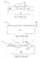
- FIG. 3shows an electron beam evaporation technique to deposit a material on a surface such as a body region of a transistor.
- a substrate 310is placed inside a deposition chamber 300 .
- the substrate in this embodimentis masked by a first masking structure 312 and a second masking structure 314 .
- the unmasked region 316includes a body region of a transistor, however one skilled in the art will recognize that other semiconductor device structures may utilize this process.
- a first electron beam source 330located within the deposition chamber 300 is a first electron beam source 330 , a first target 332 , a second electron beam source 334 , and a second target 336 .
- the multiple target configuration shownallows for compositional tuning of a number of components of the deposited material. For example, in one embodiment adjustments are available for the first target 332 evaporation rate and the second target 336 evaporation rate. The rates can be adjusted separately, allowing greater flexibility in tuning a composition of a product film 320 .
- a multiple target configurationis shown in FIG. 3 , a single target fabricated to a desired composition can also be used within the scope of the invention.
- a leak valve 340is included in the evaporation chamber 300 .
- the leak valve 340in one embodiment is connected to a source gas 342 such as oxygen.
- the leak valve 340provides another possible variable for use in tuning the composition of the product film 320 .
- the first target 332is a single element target
- the second targetis a compound target.
- compositionsincluding single element, dual element compound, or multiple element compound are possible for use in either the first target 332 , the second target 336 , or both targets.
- the first electron beam source 330generates a first electron beam 331 .
- the first electron beam 331hits the first target 332 and heats a portion of the first target 332 enough to cause the surface of the target to evaporate.
- the evaporated material 333is then distributed throughout the chamber 300 , and the material 333 deposits on surfaces that it contacts, such as the exposed body region 316 .
- the depositing material 333forms a portion of a composition in the product film 320 .
- the portion of the product film 320 being supplied by the first target 332is chemically substantially the same as the target 332 .
- a target materialincludes a metal oxide.
- the oxygen composition ratio in the product film 320varies from the target oxygen composition ratio.
- the leak valve 340may be used to adjust a variable such as oxygen composition during evaporation deposition. In this way, the oxygen composition ratio can either be adjusted back to the target oxygen composition ratio, or the oxygen composition in the product film 320 may be further varied to a new desired composition ratio.
- the product film 320includes multiple metals.
- the product film 320includes yttrium (Y) and silicon (Si).
- the first target 330is a single element yttrium metal target
- the second target 334is a compound target of silicon dioxide (SiO 2 ).
- One advantage of the thermal evaporation processis the high purity targets that are available for the process. Zone refined targets have purity as high as 99.9999%. Additionally, the evaporation process itself further purifies the target materials thus increasing the final purity of the film 320 beyond even the target purity. The more violent nature of other deposition methods such as sputtering tends to mix impurities into the deposited layer during deposition. Therefore a uniquely pure product film 320 is possible using this novel method.
- the dielectric constant of the product film 320is approximately 14, which is approximately 3.5 times the dielectric constant of SiO 2 .
- the product film 320is substantially amorphous. A lower presence of grain boundaries in the substantially amorphous material layer 320 reduces the leakage current through the final gate oxide. Although the amorphous form is preferred, the product film is also acceptable with some percentage of crystalline form.
- the yttrium-silicon-oxideexhibits a dielectric constant of approximately 14, which allows for a thinner EOT than conventional SiO 2 .
- the novel process used to form the product layer 320is performed at lower temperatures than the prior art. This inhibits reactions with the silicon substrate or other structures, and inhibits unwanted migration of elements such as dopants. In the manufacturing process of one embodiment, no subsequent oxidation steps are required after evaporation deposition.
- Microprocessor 606produces control and address signals to control the exchange of data between memory bus circuit 608 and microprocessor 606 and between memory bus circuit 608 and peripheral circuitry 610 . This exchange of data is accomplished over high speed memory bus 620 and over high speed I/O bus 622 .
- Coupled to memory bus 620are a plurality of memory slots 612 ( a-n ) which receive memory devices well known to those skilled in the art.
- memory slots 612a-n
- SIMMssingle in-line memory modules
- DIMMsdual in-line memory modules
- Page mode operations in a DRAMare defined by the method of accessing a row of a memory cell arrays and randomly accessing different columns of the array. Data stored at the row and column intersection can be read and output while that column is accessed. Page mode DRAMs require access steps which limit the communication speed of memory circuit 608 . A typical communication speed for a DRAM device using page mode is approximately 33 MHZ.
- DRAM 700interfaces with, for example, microprocessor 606 through address lines 704 and data lines 702 .
- DRAM 700may interface with a DRAM controller, a micro-controller, a chip set or other electronic system.
- Microprocessor 606also provides a number of control signals to DRAM 700 , including but not limited to, row and column address strobe signals RAS and CAS, write enable signal WE, an output enable signal OE and other conventional control signals.
- Row address buffer 712 and row decoder 714receive and decode row addresses from row address signals provided on address lines 704 by microprocessor 606 . Each unique row address corresponds to a row of cells in memory array 710 .
- Row decoder 714includes a wordline driver, an address decoder tree, and circuitry which translates a given row address received from row address buffers 712 and selectively activates the appropriate wordline of memory array 710 via the wordline drivers.
- Control logic 706is used to control the many available functions of DRAM 700 .
- various control circuits and signals not detailed hereininitiate and synchronize DRAM 700 operation as known to those skilled in the art.
- the description of DRAM 700has been simplified for purposes of illustrating the present invention and is not intended to be a complete description of all the features of a DRAM.
- a novel process of forming a gate oxidehas been shown where the surface smoothness of the body region is preserved during processing, and the resulting transistor has a smooth interface between the body region and the gate oxide with a surface roughness on the order of 0.6 nm. This solves the prior art problem of poor electrical properties such as high leakage current, created by unacceptable surface roughness.
Landscapes
- Engineering & Computer Science (AREA)
- Microelectronics & Electronic Packaging (AREA)
- Condensed Matter Physics & Semiconductors (AREA)
- General Physics & Mathematics (AREA)
- Manufacturing & Machinery (AREA)
- Computer Hardware Design (AREA)
- Physics & Mathematics (AREA)
- Power Engineering (AREA)
- Chemical & Material Sciences (AREA)
- Chemical Kinetics & Catalysis (AREA)
- Crystallography & Structural Chemistry (AREA)
- General Chemical & Material Sciences (AREA)
- Semiconductor Memories (AREA)
- Insulated Gate Type Field-Effect Transistor (AREA)
Abstract
Description
Claims (19)
Priority Applications (1)
| Application Number | Priority Date | Filing Date | Title |
|---|---|---|---|
| US10/930,138US6930346B2 (en) | 2002-03-13 | 2004-08-31 | Evaporation of Y-Si-O films for medium-K dielectrics |
Applications Claiming Priority (2)
| Application Number | Priority Date | Filing Date | Title |
|---|---|---|---|
| US10/099,194US6812100B2 (en) | 2002-03-13 | 2002-03-13 | Evaporation of Y-Si-O films for medium-k dielectrics |
| US10/930,138US6930346B2 (en) | 2002-03-13 | 2004-08-31 | Evaporation of Y-Si-O films for medium-K dielectrics |
Related Parent Applications (1)
| Application Number | Title | Priority Date | Filing Date |
|---|---|---|---|
| US10/099,194DivisionUS6812100B2 (en) | 2002-03-13 | 2002-03-13 | Evaporation of Y-Si-O films for medium-k dielectrics |
Publications (2)
| Publication Number | Publication Date |
|---|---|
| US20050026374A1 US20050026374A1 (en) | 2005-02-03 |
| US6930346B2true US6930346B2 (en) | 2005-08-16 |
Family
ID=28039531
Family Applications (2)
| Application Number | Title | Priority Date | Filing Date |
|---|---|---|---|
| US10/099,194Expired - LifetimeUS6812100B2 (en) | 2002-03-13 | 2002-03-13 | Evaporation of Y-Si-O films for medium-k dielectrics |
| US10/930,138Expired - Fee RelatedUS6930346B2 (en) | 2002-03-13 | 2004-08-31 | Evaporation of Y-Si-O films for medium-K dielectrics |
Family Applications Before (1)
| Application Number | Title | Priority Date | Filing Date |
|---|---|---|---|
| US10/099,194Expired - LifetimeUS6812100B2 (en) | 2002-03-13 | 2002-03-13 | Evaporation of Y-Si-O films for medium-k dielectrics |
Country Status (1)
| Country | Link |
|---|---|
| US (2) | US6812100B2 (en) |
Cited By (37)
| Publication number | Priority date | Publication date | Assignee | Title |
|---|---|---|---|---|
| US20050003655A1 (en)* | 1998-02-27 | 2005-01-06 | Micron Technology, Inc. | MOCVD process using ozone as a reactant to deposit a metal oxide barrier layer |
| US20050227442A1 (en)* | 2002-07-30 | 2005-10-13 | Micron Technology, Inc. | Atomic layer deposited nanolaminates of HfO2/ZrO2 films as gate dielectrics |
| US7026694B2 (en) | 2002-08-15 | 2006-04-11 | Micron Technology, Inc. | Lanthanide doped TiOx dielectric films by plasma oxidation |
| US7084078B2 (en) | 2002-08-29 | 2006-08-01 | Micron Technology, Inc. | Atomic layer deposited lanthanide doped TiOx dielectric films |
| US20060228868A1 (en)* | 2005-03-29 | 2006-10-12 | Micron Technology, Inc. | ALD of amorphous lanthanide doped TiOx films |
| US7129553B2 (en) | 2003-06-24 | 2006-10-31 | Micron Technology, Inc. | Lanthanide oxide/hafnium oxide dielectrics |
| US7135421B2 (en) | 2002-06-05 | 2006-11-14 | Micron Technology, Inc. | Atomic layer-deposited hafnium aluminum oxide |
| US7183186B2 (en) | 2003-04-22 | 2007-02-27 | Micro Technology, Inc. | Atomic layer deposited ZrTiO4 films |
| US7192892B2 (en) | 2003-03-04 | 2007-03-20 | Micron Technology, Inc. | Atomic layer deposited dielectric layers |
| US7192824B2 (en) | 2003-06-24 | 2007-03-20 | Micron Technology, Inc. | Lanthanide oxide / hafnium oxide dielectric layers |
| US7199023B2 (en) | 2002-08-28 | 2007-04-03 | Micron Technology, Inc. | Atomic layer deposited HfSiON dielectric films wherein each precursor is independendently pulsed |
| US7205218B2 (en) | 2002-06-05 | 2007-04-17 | Micron Technology, Inc. | Method including forming gate dielectrics having multiple lanthanide oxide layers |
| US7235854B2 (en) | 2002-08-15 | 2007-06-26 | Micron Technology, Inc. | Lanthanide doped TiOx dielectric films |
| US20070158863A1 (en)* | 2005-12-27 | 2007-07-12 | Dean Eshleman | Liquid crystal cells with uniform cell gap and methods of manufacture |
| US7259434B2 (en) | 2001-08-30 | 2007-08-21 | Micron Technology, Inc. | Highly reliable amorphous high-k gate oxide ZrO2 |
| US7402876B2 (en) | 2002-12-04 | 2008-07-22 | Micron Technology, Inc. | Zr— Sn—Ti—O films |
| US7410668B2 (en) | 2001-03-01 | 2008-08-12 | Micron Technology, Inc. | Methods, systems, and apparatus for uniform chemical-vapor depositions |
| US7410910B2 (en) | 2005-08-31 | 2008-08-12 | Micron Technology, Inc. | Lanthanum aluminum oxynitride dielectric films |
| US7446368B2 (en) | 2001-08-30 | 2008-11-04 | Micron Technology, Inc. | Deposition of metal oxide and/or low asymmetrical tunnel barrier interpoly insulators |
| US20090174010A1 (en)* | 2008-01-03 | 2009-07-09 | International Business Machines Corporation | Sram device structure including same band gap transistors having gate stacks with high-k dielectrics and same work function |
| US7560793B2 (en) | 2002-05-02 | 2009-07-14 | Micron Technology, Inc. | Atomic layer deposition and conversion |
| US7560395B2 (en) | 2005-01-05 | 2009-07-14 | Micron Technology, Inc. | Atomic layer deposited hafnium tantalum oxide dielectrics |
| US7563730B2 (en) | 2006-08-31 | 2009-07-21 | Micron Technology, Inc. | Hafnium lanthanide oxynitride films |
| US7572695B2 (en) | 2005-05-27 | 2009-08-11 | Micron Technology, Inc. | Hafnium titanium oxide films |
| US7588988B2 (en) | 2004-08-31 | 2009-09-15 | Micron Technology, Inc. | Method of forming apparatus having oxide films formed using atomic layer deposition |
| US7601649B2 (en) | 2004-08-02 | 2009-10-13 | Micron Technology, Inc. | Zirconium-doped tantalum oxide films |
| US7611959B2 (en) | 2002-12-04 | 2009-11-03 | Micron Technology, Inc. | Zr-Sn-Ti-O films |
| US7625794B2 (en) | 2003-03-31 | 2009-12-01 | Micron Technology, Inc. | Methods of forming zirconium aluminum oxide |
| US7662729B2 (en) | 2005-04-28 | 2010-02-16 | Micron Technology, Inc. | Atomic layer deposition of a ruthenium layer to a lanthanide oxide dielectric layer |
| US7670646B2 (en) | 2002-05-02 | 2010-03-02 | Micron Technology, Inc. | Methods for atomic-layer deposition |
| US7687409B2 (en) | 2005-03-29 | 2010-03-30 | Micron Technology, Inc. | Atomic layer deposited titanium silicon oxide films |
| US7709402B2 (en) | 2006-02-16 | 2010-05-04 | Micron Technology, Inc. | Conductive layers for hafnium silicon oxynitride films |
| US7719065B2 (en) | 2004-08-26 | 2010-05-18 | Micron Technology, Inc. | Ruthenium layer for a dielectric layer containing a lanthanide oxide |
| US7869242B2 (en) | 1999-07-30 | 2011-01-11 | Micron Technology, Inc. | Transmission lines for CMOS integrated circuits |
| US7867919B2 (en) | 2004-08-31 | 2011-01-11 | Micron Technology, Inc. | Method of fabricating an apparatus having a lanthanum-metal oxide dielectric layer |
| US8110469B2 (en) | 2005-08-30 | 2012-02-07 | Micron Technology, Inc. | Graded dielectric layers |
| US8501563B2 (en) | 2005-07-20 | 2013-08-06 | Micron Technology, Inc. | Devices with nanocrystals and methods of formation |
Families Citing this family (12)
| Publication number | Priority date | Publication date | Assignee | Title |
|---|---|---|---|---|
| US7068544B2 (en) | 2001-08-30 | 2006-06-27 | Micron Technology, Inc. | Flash memory with low tunnel barrier interpoly insulators |
| US6900122B2 (en) | 2001-12-20 | 2005-05-31 | Micron Technology, Inc. | Low-temperature grown high-quality ultra-thin praseodymium gate dielectrics |
| US7045430B2 (en)* | 2002-05-02 | 2006-05-16 | Micron Technology Inc. | Atomic layer-deposited LaAlO3 films for gate dielectrics |
| US7221017B2 (en) | 2002-07-08 | 2007-05-22 | Micron Technology, Inc. | Memory utilizing oxide-conductor nanolaminates |
| US7221586B2 (en) | 2002-07-08 | 2007-05-22 | Micron Technology, Inc. | Memory utilizing oxide nanolaminates |
| US7235501B2 (en) | 2004-12-13 | 2007-06-26 | Micron Technology, Inc. | Lanthanum hafnium oxide dielectrics |
| US7508648B2 (en) | 2005-02-08 | 2009-03-24 | Micron Technology, Inc. | Atomic layer deposition of Dy doped HfO2 films as gate dielectrics |
| US7374964B2 (en) | 2005-02-10 | 2008-05-20 | Micron Technology, Inc. | Atomic layer deposition of CeO2/Al2O3 films as gate dielectrics |
| US7498247B2 (en) | 2005-02-23 | 2009-03-03 | Micron Technology, Inc. | Atomic layer deposition of Hf3N4/HfO2 films as gate dielectrics |
| US7390756B2 (en)* | 2005-04-28 | 2008-06-24 | Micron Technology, Inc. | Atomic layer deposited zirconium silicon oxide films |
| US20070049023A1 (en)* | 2005-08-29 | 2007-03-01 | Micron Technology, Inc. | Zirconium-doped gadolinium oxide films |
| US8071476B2 (en) | 2005-08-31 | 2011-12-06 | Micron Technology, Inc. | Cobalt titanium oxide dielectric films |
Citations (78)
| Publication number | Priority date | Publication date | Assignee | Title |
|---|---|---|---|---|
| US3381114A (en) | 1963-12-28 | 1968-04-30 | Nippon Electric Co | Device for manufacturing epitaxial crystals |
| US4215156A (en) | 1977-08-26 | 1980-07-29 | International Business Machines Corporation | Method for fabricating tantalum semiconductor contacts |
| US4333808A (en) | 1979-10-30 | 1982-06-08 | International Business Machines Corporation | Method for manufacture of ultra-thin film capacitor |
| US4394673A (en) | 1980-09-29 | 1983-07-19 | International Business Machines Corporation | Rare earth silicide Schottky barriers |
| US4399424A (en) | 1980-10-07 | 1983-08-16 | Itt Industries, Inc. | Gas sensor |
| US4413022A (en) | 1979-02-28 | 1983-11-01 | Canon Kabushiki Kaisha | Method for performing growth of compound thin films |
| US4590042A (en) | 1984-12-24 | 1986-05-20 | Tegal Corporation | Plasma reactor having slotted manifold |
| US4647947A (en) | 1982-03-15 | 1987-03-03 | Tokyo Shibaura Denki Kabushiki Kaisha | Optical protuberant bubble recording medium |
| JPS62199019A (en) | 1986-02-27 | 1987-09-02 | Oki Electric Ind Co Ltd | Wafer treatment device |
| US4767641A (en) | 1986-03-04 | 1988-08-30 | Leybold-Heraeus Gmbh | Plasma treatment apparatus |
| US4920071A (en) | 1985-03-15 | 1990-04-24 | Fairchild Camera And Instrument Corporation | High temperature interconnect system for an integrated circuit |
| US4993358A (en) | 1989-07-28 | 1991-02-19 | Watkins-Johnson Company | Chemical vapor deposition reactor and method of operation |
| US5006192A (en) | 1988-06-28 | 1991-04-09 | Mitsubishi Denki Kabushiki Kaisha | Apparatus for producing semiconductor devices |
| US5055319A (en) | 1990-04-02 | 1991-10-08 | The Regents Of The University Of California | Controlled high rate deposition of metal oxide films |
| US5080928A (en) | 1990-10-05 | 1992-01-14 | Gte Laboratories Incorporated | Method for making moisture insensitive zinc sulfide based luminescent materials |
| JPH0590169A (en) | 1991-09-25 | 1993-04-09 | Hitachi Ltd | Gas feeder, and microwave plasma film forming device equipped with same |
| US5595606A (en) | 1995-04-20 | 1997-01-21 | Tokyo Electron Limited | Shower head and film forming apparatus using the same |
| US5621681A (en) | 1995-03-22 | 1997-04-15 | Samsung Electronics Co., Ltd. | Device and manufacturing method for a ferroelectric memory |
| US5698022A (en) | 1996-08-14 | 1997-12-16 | Advanced Technology Materials, Inc. | Lanthanide/phosphorus precursor compositions for MOCVD of lanthanide/phosphorus oxide films |
| US5735960A (en) | 1996-04-02 | 1998-04-07 | Micron Technology, Inc. | Apparatus and method to increase gas residence time in a reactor |
| US5795808A (en) | 1995-11-13 | 1998-08-18 | Hyundai Electronics Industries C., Ltd. | Method for forming shallow junction for semiconductor device |
| US5801105A (en) | 1995-08-04 | 1998-09-01 | Tdk Corporation | Multilayer thin film, substrate for electronic device, electronic device, and preparation of multilayer oxide thin film |
| US5810923A (en) | 1994-08-17 | 1998-09-22 | Tdk Corporation | Method for forming oxide thin film and the treatment of silicon substrate |
| US5822256A (en) | 1994-09-06 | 1998-10-13 | Intel Corporation | Method and circuitry for usage of partially functional nonvolatile memory |
| US5840897A (en) | 1990-07-06 | 1998-11-24 | Advanced Technology Materials, Inc. | Metal complex source reagents for chemical vapor deposition |
| US5916365A (en) | 1996-08-16 | 1999-06-29 | Sherman; Arthur | Sequential chemical vapor deposition |
| US5950925A (en) | 1996-10-11 | 1999-09-14 | Ebara Corporation | Reactant gas ejector head |
| US5972847A (en) | 1998-01-28 | 1999-10-26 | Lockheed Martin Energy | Method for making high-critical-current-density YBa2 Cu3 O7 superconducting layers on metallic substrates |
| US6013553A (en) | 1997-07-24 | 2000-01-11 | Texas Instruments Incorporated | Zirconium and/or hafnium oxynitride gate dielectric |
| US6020024A (en) | 1997-08-04 | 2000-02-01 | Motorola, Inc. | Method for forming high dielectric constant metal oxides |
| US6027961A (en) | 1998-06-30 | 2000-02-22 | Motorola, Inc. | CMOS semiconductor devices and method of formation |
| US6057271A (en) | 1989-12-22 | 2000-05-02 | Sumitomo Electric Industries, Ltd. | Method of making a superconducting microwave component by off-axis sputtering |
| US6059885A (en) | 1996-12-19 | 2000-05-09 | Toshiba Ceramics Co., Ltd. | Vapor deposition apparatus and method for forming thin film |
| US6093944A (en) | 1998-06-04 | 2000-07-25 | Lucent Technologies Inc. | Dielectric materials of amorphous compositions of TI-O2 doped with rare earth elements and devices employing same |
| US6110529A (en) | 1990-07-06 | 2000-08-29 | Advanced Tech Materials | Method of forming metal films on a substrate by chemical vapor deposition |
| US6161500A (en) | 1997-09-30 | 2000-12-19 | Tokyo Electron Limited | Apparatus and method for preventing the premature mixture of reactant gases in CVD and PECVD reactions |
| US6171900B1 (en) | 1999-04-15 | 2001-01-09 | Taiwan Semiconductor Manufacturing Company | CVD Ta2O5/oxynitride stacked gate insulator with TiN gate electrode for sub-quarter micron MOSFET |
| US6203613B1 (en) | 1999-10-19 | 2001-03-20 | International Business Machines Corporation | Atomic layer deposition with nitrate containing precursors |
| US6207589B1 (en) | 1999-07-19 | 2001-03-27 | Sharp Laboratories Of America, Inc. | Method of forming a doped metal oxide dielectric film |
| US6206972B1 (en) | 1999-07-08 | 2001-03-27 | Genus, Inc. | Method and apparatus for providing uniform gas delivery to substrates in CVD and PECVD processes |
| US6211035B1 (en) | 1998-09-09 | 2001-04-03 | Texas Instruments Incorporated | Integrated circuit and method |
| US6225168B1 (en) | 1998-06-04 | 2001-05-01 | Advanced Micro Devices, Inc. | Semiconductor device having metal gate electrode and titanium or tantalum nitride gate dielectric barrier layer and process of fabrication thereof |
| US6232847B1 (en) | 1997-04-28 | 2001-05-15 | Rockwell Science Center, Llc | Trimmable singleband and tunable multiband integrated oscillator using micro-electromechanical system (MEMS) technology |
| US20010009695A1 (en) | 2000-01-18 | 2001-07-26 | Saanila Ville Antero | Process for growing metalloid thin films |
| US6281144B1 (en) | 1997-09-26 | 2001-08-28 | Novellus Systems, Inc. | Exclusion of polymer film from semiconductor wafer edge and backside during film (CVD) deposition |
| US6297539B1 (en) | 1999-07-19 | 2001-10-02 | Sharp Laboratories Of America, Inc. | Doped zirconia, or zirconia-like, dielectric film transistor structure and deposition method for same |
| US6297516B1 (en) | 1997-11-24 | 2001-10-02 | The Trustees Of Princeton University | Method for deposition and patterning of organic thin film |
| US6302964B1 (en) | 1998-06-16 | 2001-10-16 | Applied Materials, Inc. | One-piece dual gas faceplate for a showerhead in a semiconductor wafer processing system |
| US6303481B2 (en) | 1999-12-29 | 2001-10-16 | Hyundai Electronics Industries Co., Ltd. | Method for forming a gate insulating film for semiconductor devices |
| JP2001332546A (en) | 2000-05-24 | 2001-11-30 | Rohm Co Ltd | Oxidizing method, manufacturing method of silicon oxide film, and oxidizing device |
| US20010051442A1 (en) | 1998-03-03 | 2001-12-13 | Dina Katsir | Method for producing high surface area foil electrodes |
| US20010053082A1 (en) | 1999-12-22 | 2001-12-20 | Makarand H. Chipalkatti | Electroluminescent vehicle lamp |
| US6348386B1 (en) | 2001-04-16 | 2002-02-19 | Motorola, Inc. | Method for making a hafnium-based insulating film |
| US20020022156A1 (en) | 1998-11-02 | 2002-02-21 | 3M Innovative Properties Company | Transparent conductive oxides for plastic flat panel displays |
| US6368941B1 (en) | 2000-11-08 | 2002-04-09 | United Microelectronics Corp. | Fabrication of a shallow trench isolation by plasma oxidation |
| US6380579B1 (en) | 1999-04-12 | 2002-04-30 | Samsung Electronics Co., Ltd. | Capacitor of semiconductor device |
| US6387712B1 (en) | 1996-06-26 | 2002-05-14 | Tdk Corporation | Process for preparing ferroelectric thin films |
| US6391769B1 (en) | 1998-08-19 | 2002-05-21 | Samsung Electronics Co., Ltd. | Method for forming metal interconnection in semiconductor device and interconnection structure fabricated thereby |
| US20020089023A1 (en) | 2001-01-05 | 2002-07-11 | Motorola, Inc. | Low leakage current metal oxide-nitrides and method of fabricating same |
| US6420279B1 (en) | 2001-06-28 | 2002-07-16 | Sharp Laboratories Of America, Inc. | Methods of using atomic layer deposition to deposit a high dielectric constant material on a substrate |
| US6432779B1 (en) | 2000-05-18 | 2002-08-13 | Motorola, Inc. | Selective removal of a metal oxide dielectric |
| US20020119297A1 (en) | 1998-08-19 | 2002-08-29 | Forrest Stephen R. | Organic photosensitive optoelectronic devices with transparent electrodes |
| US6444039B1 (en) | 2000-03-07 | 2002-09-03 | Simplus Systems Corporation | Three-dimensional showerhead apparatus |
| US6445023B1 (en) | 1999-03-16 | 2002-09-03 | Micron Technology, Inc. | Mixed metal nitride and boride barrier layers |
| US6444895B1 (en) | 1998-09-28 | 2002-09-03 | Nec Corporation | Device and method for nondestructive inspection on semiconductor device |
| US6448192B1 (en) | 2001-04-16 | 2002-09-10 | Motorola, Inc. | Method for forming a high dielectric constant material |
| US6451695B2 (en) | 1999-03-11 | 2002-09-17 | Genus, Inc. | Radical-assisted sequential CVD |
| US6451641B1 (en) | 2002-02-27 | 2002-09-17 | Advanced Micro Devices, Inc. | Non-reducing process for deposition of polysilicon gate electrode over high-K gate dielectric material |
| US6458701B1 (en) | 1999-10-20 | 2002-10-01 | Samsung Electronics Co., Ltd. | Method for forming metal layer of semiconductor device using metal halide gas |
| US20020146916A1 (en) | 2001-03-29 | 2002-10-10 | Kiyoshi Irino | Semiconductor device having a high-dielectric gate insulation film and fabrication process thereof |
| US6465334B1 (en) | 2000-10-05 | 2002-10-15 | Advanced Micro Devices, Inc. | Enhanced electroless deposition of dielectric precursor materials for use in in-laid gate MOS transistors |
| US20020155688A1 (en) | 2001-04-20 | 2002-10-24 | Ahn Kie Y. | Highly reliable gate oxide and method of fabrication |
| US6482740B2 (en) | 2000-05-15 | 2002-11-19 | Asm Microchemistry Oy | Method of growing electrical conductors by reducing metal oxide film with organic compound containing -OH, -CHO, or -COOH |
| US6495436B2 (en) | 2001-02-09 | 2002-12-17 | Micron Technology, Inc. | Formation of metal oxide gate dielectric |
| US20020192974A1 (en) | 2001-06-13 | 2002-12-19 | Ahn Kie Y. | Dielectric layer forming method and devices formed therewith |
| US20030001241A1 (en) | 2000-01-18 | 2003-01-02 | Agere Systems Guardian Corp. | Semiconductor device and method of fabrication |
| US20030017717A1 (en) | 2001-07-18 | 2003-01-23 | Ahn Kie Y. | Methods for forming dielectric materials and methods for forming semiconductor devices |
| US6521911B2 (en) | 2000-07-20 | 2003-02-18 | North Carolina State University | High dielectric constant metal silicates formed by controlled metal-surface reactions |
Family Cites Families (16)
| Publication number | Priority date | Publication date | Assignee | Title |
|---|---|---|---|---|
| JPS5090169A (en) | 1973-12-13 | 1975-07-19 | ||
| US5198029A (en) | 1989-08-01 | 1993-03-30 | Gte Products Corporation | Apparatus for coating small solids |
| US5825560A (en)* | 1995-02-28 | 1998-10-20 | Canon Kabushiki Xaisha | Optical apparatus |
| US6166866A (en)* | 1995-02-28 | 2000-12-26 | Canon Kabushiki Kaisha | Reflecting type optical system |
| US6021004A (en)* | 1995-02-28 | 2000-02-01 | Canon Kabushiki Kaisha | Reflecting type of zoom lens |
| US6522475B2 (en)* | 1996-02-15 | 2003-02-18 | Canon Kabushiki Kaisha | Zoom lens |
| US5999311A (en)* | 1996-03-26 | 1999-12-07 | Canon Kabushiki Kaisha | Small-sized variable magnification optical system |
| JP2000162502A (en)* | 1998-09-21 | 2000-06-16 | Canon Inc | Optical system and optical apparatus having the same |
| JP2001066504A (en)* | 1999-08-30 | 2001-03-16 | Canon Inc | Optical element and imaging device using the same |
| JP2002008853A (en)* | 2000-06-16 | 2002-01-11 | Nippon Seiki Co Ltd | Organic EL panel |
| JP2002018289A (en)* | 2000-06-30 | 2002-01-22 | Tsurushou:Kk | Method for activating water by catalyst resin |
| JP2002105734A (en)* | 2000-10-03 | 2002-04-10 | Starlite Co Ltd | Helmet |
| JP2002149854A (en)* | 2000-11-16 | 2002-05-24 | Kubo Hikari | Information collection system |
| US6484740B2 (en)* | 2001-02-14 | 2002-11-26 | Clinton Guthrie | Blower assembly for gas wells |
| JP2003007255A (en)* | 2001-06-20 | 2003-01-10 | Kojima Press Co Ltd | Battery jar for secondary battery, and manufacturing method of battery jar for the secondary battery |
| JP3742767B2 (en)* | 2001-10-29 | 2006-02-08 | ポーラ化成工業株式会社 | Hair conditioner consisting of extracts of Asagaokakaraksa and other herbal extracts |
- 2002
- 2002-03-13USUS10/099,194patent/US6812100B2/ennot_activeExpired - Lifetime
- 2004
- 2004-08-31USUS10/930,138patent/US6930346B2/ennot_activeExpired - Fee Related
Patent Citations (85)
| Publication number | Priority date | Publication date | Assignee | Title |
|---|---|---|---|---|
| US3381114A (en) | 1963-12-28 | 1968-04-30 | Nippon Electric Co | Device for manufacturing epitaxial crystals |
| US4215156A (en) | 1977-08-26 | 1980-07-29 | International Business Machines Corporation | Method for fabricating tantalum semiconductor contacts |
| US4413022A (en) | 1979-02-28 | 1983-11-01 | Canon Kabushiki Kaisha | Method for performing growth of compound thin films |
| US4333808A (en) | 1979-10-30 | 1982-06-08 | International Business Machines Corporation | Method for manufacture of ultra-thin film capacitor |
| US4394673A (en) | 1980-09-29 | 1983-07-19 | International Business Machines Corporation | Rare earth silicide Schottky barriers |
| US4399424A (en) | 1980-10-07 | 1983-08-16 | Itt Industries, Inc. | Gas sensor |
| US4647947A (en) | 1982-03-15 | 1987-03-03 | Tokyo Shibaura Denki Kabushiki Kaisha | Optical protuberant bubble recording medium |
| US4590042A (en) | 1984-12-24 | 1986-05-20 | Tegal Corporation | Plasma reactor having slotted manifold |
| US4920071A (en) | 1985-03-15 | 1990-04-24 | Fairchild Camera And Instrument Corporation | High temperature interconnect system for an integrated circuit |
| JPS62199019A (en) | 1986-02-27 | 1987-09-02 | Oki Electric Ind Co Ltd | Wafer treatment device |
| US4767641A (en) | 1986-03-04 | 1988-08-30 | Leybold-Heraeus Gmbh | Plasma treatment apparatus |
| US5006192A (en) | 1988-06-28 | 1991-04-09 | Mitsubishi Denki Kabushiki Kaisha | Apparatus for producing semiconductor devices |
| US4993358A (en) | 1989-07-28 | 1991-02-19 | Watkins-Johnson Company | Chemical vapor deposition reactor and method of operation |
| US6057271A (en) | 1989-12-22 | 2000-05-02 | Sumitomo Electric Industries, Ltd. | Method of making a superconducting microwave component by off-axis sputtering |
| US5055319A (en) | 1990-04-02 | 1991-10-08 | The Regents Of The University Of California | Controlled high rate deposition of metal oxide films |
| US6110529A (en) | 1990-07-06 | 2000-08-29 | Advanced Tech Materials | Method of forming metal films on a substrate by chemical vapor deposition |
| US5840897A (en) | 1990-07-06 | 1998-11-24 | Advanced Technology Materials, Inc. | Metal complex source reagents for chemical vapor deposition |
| US5080928A (en) | 1990-10-05 | 1992-01-14 | Gte Laboratories Incorporated | Method for making moisture insensitive zinc sulfide based luminescent materials |
| JPH0590169A (en) | 1991-09-25 | 1993-04-09 | Hitachi Ltd | Gas feeder, and microwave plasma film forming device equipped with same |
| US5810923A (en) | 1994-08-17 | 1998-09-22 | Tdk Corporation | Method for forming oxide thin film and the treatment of silicon substrate |
| US5828080A (en) | 1994-08-17 | 1998-10-27 | Tdk Corporation | Oxide thin film, electronic device substrate and electronic device |
| US5822256A (en) | 1994-09-06 | 1998-10-13 | Intel Corporation | Method and circuitry for usage of partially functional nonvolatile memory |
| US5621681A (en) | 1995-03-22 | 1997-04-15 | Samsung Electronics Co., Ltd. | Device and manufacturing method for a ferroelectric memory |
| US5744374A (en) | 1995-03-22 | 1998-04-28 | Samsung Electronics Co., Ltd. | Device and manufacturing method for a ferroelectric memory |
| US5595606A (en) | 1995-04-20 | 1997-01-21 | Tokyo Electron Limited | Shower head and film forming apparatus using the same |
| US5801105A (en) | 1995-08-04 | 1998-09-01 | Tdk Corporation | Multilayer thin film, substrate for electronic device, electronic device, and preparation of multilayer oxide thin film |
| US5795808A (en) | 1995-11-13 | 1998-08-18 | Hyundai Electronics Industries C., Ltd. | Method for forming shallow junction for semiconductor device |
| US5735960A (en) | 1996-04-02 | 1998-04-07 | Micron Technology, Inc. | Apparatus and method to increase gas residence time in a reactor |
| US6387712B1 (en) | 1996-06-26 | 2002-05-14 | Tdk Corporation | Process for preparing ferroelectric thin films |
| US5698022A (en) | 1996-08-14 | 1997-12-16 | Advanced Technology Materials, Inc. | Lanthanide/phosphorus precursor compositions for MOCVD of lanthanide/phosphorus oxide films |
| US5916365A (en) | 1996-08-16 | 1999-06-29 | Sherman; Arthur | Sequential chemical vapor deposition |
| US5950925A (en) | 1996-10-11 | 1999-09-14 | Ebara Corporation | Reactant gas ejector head |
| US6059885A (en) | 1996-12-19 | 2000-05-09 | Toshiba Ceramics Co., Ltd. | Vapor deposition apparatus and method for forming thin film |
| US6232847B1 (en) | 1997-04-28 | 2001-05-15 | Rockwell Science Center, Llc | Trimmable singleband and tunable multiband integrated oscillator using micro-electromechanical system (MEMS) technology |
| US6013553A (en) | 1997-07-24 | 2000-01-11 | Texas Instruments Incorporated | Zirconium and/or hafnium oxynitride gate dielectric |
| US6291866B1 (en) | 1997-07-24 | 2001-09-18 | Texas Instruments Incorporated | Zirconium and/or hafnium oxynitride gate dielectric |
| US6020024A (en) | 1997-08-04 | 2000-02-01 | Motorola, Inc. | Method for forming high dielectric constant metal oxides |
| US6281144B1 (en) | 1997-09-26 | 2001-08-28 | Novellus Systems, Inc. | Exclusion of polymer film from semiconductor wafer edge and backside during film (CVD) deposition |
| US6161500A (en) | 1997-09-30 | 2000-12-19 | Tokyo Electron Limited | Apparatus and method for preventing the premature mixture of reactant gases in CVD and PECVD reactions |
| US6297516B1 (en) | 1997-11-24 | 2001-10-02 | The Trustees Of Princeton University | Method for deposition and patterning of organic thin film |
| US5972847A (en) | 1998-01-28 | 1999-10-26 | Lockheed Martin Energy | Method for making high-critical-current-density YBa2 Cu3 O7 superconducting layers on metallic substrates |
| US20010051442A1 (en) | 1998-03-03 | 2001-12-13 | Dina Katsir | Method for producing high surface area foil electrodes |
| US6225168B1 (en) | 1998-06-04 | 2001-05-01 | Advanced Micro Devices, Inc. | Semiconductor device having metal gate electrode and titanium or tantalum nitride gate dielectric barrier layer and process of fabrication thereof |
| US6093944A (en) | 1998-06-04 | 2000-07-25 | Lucent Technologies Inc. | Dielectric materials of amorphous compositions of TI-O2 doped with rare earth elements and devices employing same |
| US6302964B1 (en) | 1998-06-16 | 2001-10-16 | Applied Materials, Inc. | One-piece dual gas faceplate for a showerhead in a semiconductor wafer processing system |
| US6027961A (en) | 1998-06-30 | 2000-02-22 | Motorola, Inc. | CMOS semiconductor devices and method of formation |
| US6391769B1 (en) | 1998-08-19 | 2002-05-21 | Samsung Electronics Co., Ltd. | Method for forming metal interconnection in semiconductor device and interconnection structure fabricated thereby |
| US20020119297A1 (en) | 1998-08-19 | 2002-08-29 | Forrest Stephen R. | Organic photosensitive optoelectronic devices with transparent electrodes |
| US6211035B1 (en) | 1998-09-09 | 2001-04-03 | Texas Instruments Incorporated | Integrated circuit and method |
| US6444895B1 (en) | 1998-09-28 | 2002-09-03 | Nec Corporation | Device and method for nondestructive inspection on semiconductor device |
| US20020022156A1 (en) | 1998-11-02 | 2002-02-21 | 3M Innovative Properties Company | Transparent conductive oxides for plastic flat panel displays |
| US6451695B2 (en) | 1999-03-11 | 2002-09-17 | Genus, Inc. | Radical-assisted sequential CVD |
| US6445023B1 (en) | 1999-03-16 | 2002-09-03 | Micron Technology, Inc. | Mixed metal nitride and boride barrier layers |
| US6380579B1 (en) | 1999-04-12 | 2002-04-30 | Samsung Electronics Co., Ltd. | Capacitor of semiconductor device |
| US6171900B1 (en) | 1999-04-15 | 2001-01-09 | Taiwan Semiconductor Manufacturing Company | CVD Ta2O5/oxynitride stacked gate insulator with TiN gate electrode for sub-quarter micron MOSFET |
| US6206972B1 (en) | 1999-07-08 | 2001-03-27 | Genus, Inc. | Method and apparatus for providing uniform gas delivery to substrates in CVD and PECVD processes |
| US6207589B1 (en) | 1999-07-19 | 2001-03-27 | Sharp Laboratories Of America, Inc. | Method of forming a doped metal oxide dielectric film |
| US6297539B1 (en) | 1999-07-19 | 2001-10-02 | Sharp Laboratories Of America, Inc. | Doped zirconia, or zirconia-like, dielectric film transistor structure and deposition method for same |
| US6203613B1 (en) | 1999-10-19 | 2001-03-20 | International Business Machines Corporation | Atomic layer deposition with nitrate containing precursors |
| US6458701B1 (en) | 1999-10-20 | 2002-10-01 | Samsung Electronics Co., Ltd. | Method for forming metal layer of semiconductor device using metal halide gas |
| US20010053082A1 (en) | 1999-12-22 | 2001-12-20 | Makarand H. Chipalkatti | Electroluminescent vehicle lamp |
| US6303481B2 (en) | 1999-12-29 | 2001-10-16 | Hyundai Electronics Industries Co., Ltd. | Method for forming a gate insulating film for semiconductor devices |
| US20030001241A1 (en) | 2000-01-18 | 2003-01-02 | Agere Systems Guardian Corp. | Semiconductor device and method of fabrication |
| US20010009695A1 (en) | 2000-01-18 | 2001-07-26 | Saanila Ville Antero | Process for growing metalloid thin films |
| US6444039B1 (en) | 2000-03-07 | 2002-09-03 | Simplus Systems Corporation | Three-dimensional showerhead apparatus |
| US6482740B2 (en) | 2000-05-15 | 2002-11-19 | Asm Microchemistry Oy | Method of growing electrical conductors by reducing metal oxide film with organic compound containing -OH, -CHO, or -COOH |
| US6432779B1 (en) | 2000-05-18 | 2002-08-13 | Motorola, Inc. | Selective removal of a metal oxide dielectric |
| JP2001332546A (en) | 2000-05-24 | 2001-11-30 | Rohm Co Ltd | Oxidizing method, manufacturing method of silicon oxide film, and oxidizing device |
| US6521911B2 (en) | 2000-07-20 | 2003-02-18 | North Carolina State University | High dielectric constant metal silicates formed by controlled metal-surface reactions |
| US6465334B1 (en) | 2000-10-05 | 2002-10-15 | Advanced Micro Devices, Inc. | Enhanced electroless deposition of dielectric precursor materials for use in in-laid gate MOS transistors |
| US6368941B1 (en) | 2000-11-08 | 2002-04-09 | United Microelectronics Corp. | Fabrication of a shallow trench isolation by plasma oxidation |
| US20020089023A1 (en) | 2001-01-05 | 2002-07-11 | Motorola, Inc. | Low leakage current metal oxide-nitrides and method of fabricating same |
| US20030003702A1 (en) | 2001-02-09 | 2003-01-02 | Micron Technology, Inc. | Formation of metal oxide gate dielectric |
| US6495436B2 (en) | 2001-02-09 | 2002-12-17 | Micron Technology, Inc. | Formation of metal oxide gate dielectric |
| US20020146916A1 (en) | 2001-03-29 | 2002-10-10 | Kiyoshi Irino | Semiconductor device having a high-dielectric gate insulation film and fabrication process thereof |
| US6448192B1 (en) | 2001-04-16 | 2002-09-10 | Motorola, Inc. | Method for forming a high dielectric constant material |
| US6348386B1 (en) | 2001-04-16 | 2002-02-19 | Motorola, Inc. | Method for making a hafnium-based insulating film |
| US20020155689A1 (en) | 2001-04-20 | 2002-10-24 | Ahn Kie Y. | Highly reliable gate oxide and method of fabrication |
| US20020155688A1 (en) | 2001-04-20 | 2002-10-24 | Ahn Kie Y. | Highly reliable gate oxide and method of fabrication |
| US6514828B2 (en) | 2001-04-20 | 2003-02-04 | Micron Technology, Inc. | Method of fabricating a highly reliable gate oxide |
| US20020192974A1 (en) | 2001-06-13 | 2002-12-19 | Ahn Kie Y. | Dielectric layer forming method and devices formed therewith |
| US6420279B1 (en) | 2001-06-28 | 2002-07-16 | Sharp Laboratories Of America, Inc. | Methods of using atomic layer deposition to deposit a high dielectric constant material on a substrate |
| US20030017717A1 (en) | 2001-07-18 | 2003-01-23 | Ahn Kie Y. | Methods for forming dielectric materials and methods for forming semiconductor devices |
| US6534420B2 (en) | 2001-07-18 | 2003-03-18 | Micron Technology, Inc. | Methods for forming dielectric materials and methods for forming semiconductor devices |
| US6451641B1 (en) | 2002-02-27 | 2002-09-17 | Advanced Micro Devices, Inc. | Non-reducing process for deposition of polysilicon gate electrode over high-K gate dielectric material |
Non-Patent Citations (99)
| Title |
|---|
| Aarik, Jaan , et al., "Atomic layer growth of epitaxial TiO/sub 2/ thin films from TiCl/sub 4/ and H/sub 2/O on alpha -Al/sub 2/O/sub 3/ substrates", Journal Crystal Growth, 242(1-2), (2002), 189-198. |
| Aarik, Jaan , et al., "Influence of substrate temperature on atomic layer growth and properties of HfO/sub 2/ thin films", Thin Solid Films, 340(1-2), (1999),110-116. |
| Aarik, Jaan , et al., "Phase transformations in hafnium dioxide thin films grown by atomic layer doposition at high temperatures", Applied Surface Science, 173(1-2), (Mar. 2001),15-21. |
| Aarik, Jaan , et al., "Texture Development in nanocrystalline hafnium dioxide thin films grown by atomic layer deposition", Journal of Crystal Growth, 220, (2000), 105-113. |
| Alen, Petra , "Atomic Layer deposition of Ta(Al)N(C) thin films using trimethylaluminum as a reducing agent", Journal of the Electrochemical Society, 148(10), (Oct. 2001),G566-G571. |
| Bendoraitis, J G., et al., "Optical energy gaps in the monoclinic oxides of hafnium and zirconium and their solid solutions", Journal of Physical Chemistry, 69(10), (1965),3666-3667. |
| Bright, A A., et al., "Low-rate plasma oxidation of Si in a dilute oxygen/helium plasma for low-temperature gate quality Si/Sio2 interfaces", Applied Physics Letters, 58(6), (Feb. 1991),619-621. |
| Bunshah, Rointan F., et al., "Deposition Technologies for Films and Coatings: Developments and Applications", Park Ridge, N.J., U.S.A. ; Noves Publications, (1982),102-103. |
| Cava, RJ., "Improvement of the dielectric properties of Ta/sub 2/O/sub 5/ through substitution with Al/sub 2/O/sub 3/", Applied Physics Letters, 70(11), (Mar. 1997),1396-8. |
| Chambers, J J., et al., "Physical and electrical characterization of ultrathin yttrium silicate insulators on silicon", Journal of Applied Physics, 90(2), (Jul. 15, 2001),918-33. |
| Cheng, Baohong , et al., "The Impact of High-k Gate Dielectrics and Metal Gate Electrodes on Sub-100nm MOSFET's", IEEE Transactions on Electron Devices, 46(7), (Jul. 1999), 1537-1544. |
| Copel, M. , "Structure and stability of ultrathin zirconium oxide layers on Si(001)", Applied Physics Letters, 76(4), (Jan. 2000),436-438. |
| De Flaviis, Franco , et al., "Planar microwave integrated phase-shifter design with high purity ferroelectric material", IEEE Transactions on Microwave Theory & Techniques, 45(6), (Jun. 1997),963-969. |
| Desu, S B., "Minimization of Fatigue in Ferroelectric Films", Physica Status Solidi A, 151(2), (1995),467-480. |
| Dusco, C , et al., "Deposition of tin oxide into porous silicon by atomic layer epitaxy", Journal of the Electrochemical Society, 143, (1996),683-687. |
| El-Kareh, B , et al., "The evolution of DRAM cell technology", Solid State Technology, 40(5), (1997),89-90, 92, 95-6, 98, 100-1. |
| Engelhardt, M. , "Modern Applications of Plasma Etching and Patterning in Silicon Process Technology", Contributions to Plasma Physics, 39(5), (1999),473-478. |
| Forsgren, Katarina , "Atomic Layer Deposition of HfO2 using hafhium iodide", Conference held in Monterey, California, (May 2001), 1 page. |
| Fuyuki, Takashi , et al., "Electronic Properties of the Interface between Si and TiO2 Deposited at Very Low Temperatures", Japanese Journal of Applied Physics, Part 1 (Regular Papers & Short Notes), 25(9), (Sep. 1986),1288-1291. |
| Fuyuki, Takashi , et al., "Initial stage of ultra-thin SiO/sub 2/ formation at low temperatures using activated oxygen", Applied Surface Science, 117-118, (Jun. 1997),123-126. |
| Gartner, M , et al., "Spectroellipsometric characterization of lanthanide-doped TiO2 films obtained via the sol-gel technique", Thin Solid Films, 234(1-2), (1993),561-565. |
| Geller, S. , et al., "Crystallographic Studies of Perovskite-like Compounds. II. Rare Earth Aluminates", Acta Cryst., 9, (May 1956),1019-1025. |
| Giess, E. A., et al., "Lanthanide gallate perovskite-type substates for epitaxial, high-T/sub c/ superconducting Ba/sub 2/YCu/sub 3/O/sub 7-delta / films", IBM Journal of Research and Development, 34(6), (Nov. 1990),916-926. |
| Guillaumot, B , et al., "75 nm damascene metal gate and high-k integration for advanced CMOS devices", Technical Digest of International Electron Devices Meeting 2002, (2002),355-358. |
| Gusev, E P., et al., "Ultrathin High-K Dielectrics Grown by Atomic Layer Deposition: A Comparative Study of ZrO2, HfO2, Y2O3 and Al2O3", Eletrochemical Society Proceedings vol. 2001-9, (2001)189-195. |
| Gutowski, M J., "Thermodynamic stability of high-K dielectric metal oxides ZrO/sub 2/ and HfO/sub 2/ in contact with Si and SiO/sub 2/", Applied Physics Letters, 80(11), (Mar. 18, 2002), 1897-1899. |
| Hirayama, Masaki , et al., "Low-Temperature Growth of High-Integrity Silicon Oxide Films by Oxygen Radical Generated in High Density Krypton Plasma", International Electron Devices Meeting 1999, Technical Digest, (1999),249-252. |
| Hubbard, K. J., "Thermodynamic stability of binary oxides in contact with silicon", Journal of Materials Research, 11(11), (Nov. 1996),2757-2776. |
| Hunt, C. E., et al., "Direct bonding of micromachined silicon wafers for laser diode heat exchanger applications", Journal of Micromechanics and Microengineering, 1(3), (Sep. 1991), 152-156. |
| Iddles, D M., et al., "Relationships between dopants, microstructure and the microwave dielectric properties of ZrO2-TiO2-SnO2 ceramics", Journal of Materials Science, 27(23), (Dec. 1992),6303-6310. |
| Jeon, Sanghun , et al., "Excellent electrical characteristics of lanthanide (Pr, Nd, Sm, Gd, and Dy) oxide and lanthanide-doped oxide for MOS gate dielectric applications", Electron Devices Meeting, 2001. IEDM Technical Digest. International, (2000),471-474. |
| Jeong, Chang-Wook , et al., "Plasma-Assisted Atomic Layer Growth of High-Quality Aluminum Oxide Thin Films", Japanese Journal of Applied Physics, Part 1: Regular Papers and Short Notes and Review Papers, 40(1), (Jan. 2001),285-289. |
| Jung, H S., et al., "Improved current performance of CMOSFETs with nitrogen incorporated HfO/sub 2/-Al/sub 3/ laminate gate dielectric", Technical Digest of International Electron Devices Meeting 2002, (2002),853-856. |
| Kang, L , et al., "MOSFET devices with polysilicon on single-layer HfO/sub 2/ high-K dielectrics", International Electron Devices Meeting 2000. Technical Digest. IEDM, (2000),35-8. |
| Kawai, Y, et al., "Ultra-low-temperature growth of high-integrity gate oxide films by low-energy Ion-assisted oxidation", Applied Physics Letters, 64(17), (Apr. 1994),2223-2225. |
| Keomany, D , et al., "Sol gel preparation of mixed cerium-titanium oxide thin films", Solar Energy Materials and Solar Cells, 33(4), (Aug. 1994),429-441. |
| Kim, Byoung-Youp , et al., "Comparison Study for TiN films deposited from different method: chemical vapor deposition and atomic layer deposition", Mechanisms of Surface and Microstructure Evolution in Deposited Films and Film Structures Symposium (Materials Research Society Symposium Proceedings vol. 672), (2001),7.8.1-7.8.6. |
| Kim, C T., et al., "Application of Al2O3 Grown by Atomic Layer Deposition to DRAM and FeRAM", International Symposium in Integrated Ferroelectrics, (Mar. 2000),316. |
| Kim, D. , et al., "Atomic Control of Substrate Termination and Heteroepitaxial Growth of SrTiO3/LaAlO3 Films", Journal of the Korean Physical Society, 36(6), (Jun. 2000),444-448. |
| Kim, Taeseok , et al., "Correlation between strain and dielectric properties in ZrTiO/sub 4/ thin films", Applied Physics Letters, 76(21), (May 2000),3043-3045. |
| Kim, Taeseok , et al., "Dielectric properties and strain analysis in paraelectric ZrTiO/sub 4/ thin films deposited by DC magnetron sputtering", Japanese Journal of Applied Physics Part 1-Regular Papers Short Notes & Review Papers, 39(7A), (2000),4153-4157. |
| Kim, Y , et al., "Substrate dependence on the optical properties of Al/sub 2/O/sub 3/ films grown by atomic layer deposition", Applied Physics Letters, 71(25, 22 ), (Dec. 1997),3604-3606. |
| Kim, Y W., et al., "50nm gate length logic technology with 9-layer Cu interconnects for 90nm node SoC applications", Technical Digest of International Electron Devices Meeting 2002, (2002),69-72. |
| Kim, Yongjo , et al., "Effect of microstructures on the microwave dielectric properties of ZrTiO/sub 4/ thin films", Applied Physics Letters, 78(16), (Apr. 16, 2001),2363-2365. |
| Krauter, G. , et al., "Room Temperature Silicon Wafer Bonding with Ultra-Thin Polymer Films", Advanced Materials, 9(5), (1997),417-420. |
| Kukli, K , et al., "Comparison of hafnium oxide films grown by atomic layer deposition from iodide and chloride and chloride precursors", Thin Solid Films, 416,(2002),72-79. |
| Kukli, K , et al., "Controlled growth of yttrium oxysulphide thing films by atomic layer deposition", Materials Science Forum, 315-317, (1999),216-221. |
| Kukli, K J., et al., "Properties of hafnium oxide films grown by atomic layer deposition from hafnium tetraiodide and oxygen", Journal of Applied Physics, 92(10), (Nov. 15, 2002),5698-5703. |
| Kukli, Kaupo , "Atomic Layer Deposition of Titanium Oxide from Til4 and H2O2", Chemical Vapor Deposition, 6(6), (2000),303-310. |
| Kukli, Kaupo , "Dielectric Properties of Zirconium Oxide Grown by Atomic Layer Deposition from Iodide Precursor", Journal of The Electrochemical Society, 148(12), (2001),F227-F232. |
| Kukli, Kaupo , et al., "Influence of thickness and growth temperature of the properties of zirconium oxide films growth by atomic layer deposition on silicon", Thin Solid Films, 410(1-2), (2002),53-60. |
| Kukli, Kaupo , et al., "Low-Temperature Deposition of Zirconium Oxide-Based Nanocrystalline Films by Alternate Supply of Zr[OC(CH3)3]4 and H2O", Chemical Vapor Deposition, 6(6), (2000),297-302. |
| Lee, A E., et al., "Epitaxyially grown sputtered LaAlO3 films", Applied Physics Letters, 57(19), (Nov. 1990),2019-2021. |
| Lee, Byoung H., et al., "Characteristics of TaN gate MOSFET with ultrathin hafnium oxide (8 A-12 A)", Electron Devices Meeting, 2000, IEDM Technical Digest. International, (2000),39-42. |
| Lee, Byoung H., et al., "Ultrathin Hafnium Oxide with Low Leakage and Excellent Reliability for Alternative Gate Dielectric Application", Technical Digest of IEDM, (1999),133-136. |
| Lee, C. H., et al., "MOS Characteristics of Ultra Thin Rapid Thermal CVD ZrO2 and Zr Silicate Gate Dielectrics", Electron Devices Meeting, 2000. IEDM Technical Digest. International, (2000),27-30. |
| Lee, C. H., et al., "MOS Devices with High Quality Ultra Thin CVD ZrO2 Gate Dielectrics and Self-Aligned TaN and TaN/Poly-Si Gate electrodes", 2001 Symposium on VLSI, Technology Digest of Technicl Papers, (2001),137-138. |
| Lee, Cheng-Chung , et al., "Ion-assisted deposition of silver thin films", Thin Solid Films, 359(1), (Jan. 2000),95-97. |
| Lee, Dong H., et al., "Metalorganic chemical vapor deposition of TiO/sub 2/:N anatase thin film on Si substrate", Applied Physics Letters, 66(7), (Feb. 1995),815-816. |
| Lee, Jung-Hyoung , et al., "Mass production worthy HfO/sub 2/-Al/sub 2/O/sub 3/ laminate capacitor technology using Hf liquid precursor for sub-100 nm DRAMs", Electron Devices Meeting, 2002. IEDM '02. Digest. International, (2002),221-224. |
| Lee, L P., et al., "Monolithic 77 K dc SQUID magnetometer", Applied Physics Letters, 59(23), (Dec. 1991),3051-3053. |
| Lee, S J., et al., "High quality ultra thin CVD HfO2 gate stack with poly-Si gate electrode", Electron Devices Meeting, 2000. IEDM Technical Digest. International, (2000),31-34. |
| Leskela, M , et al., "ALD precursor chemistry: Evolution and future challenges", Journal de Physique IV (Proceedings), 9(8), (Sep. 1999),837-852. |
| Liu, C. T., "Circuit Requirement and Integration Challenges of Thin Gate Dielectrics for Ultra Small MOSFETs", International Electron Devices Meeting 1998. Technical Digest, (1998),747-750. |
| Liu, Y C., et al., "Growth of ultrathin SiO/sub 2/ on Si by surface irradiation with an O/sub 2/+Ar electron cyclotron resonance microwave plasma at low temperatures",Journal of Applied Physics, 85(3), (Feb. 1999),1911-1915. |
| Lucovsky, G , et al., "Microscopic model for enhanced dielectric constants in low concentration SiO/sub 2/-rich noncrystalline Zr and Hf silicate alloys", Applied Physics Letters, 77(18), (Oct. 2000).2912-2914. |
| Luo, Z J., et al., "Ultra-thin ZrO2 (or Silicate) with High Thermal Stability for CMOS GAte Applications", 2001 Symposium on VLSI Technology Digest of Technical Papers, (2001),135-136. |
| Martin, P J., et al., "Ion-beam-assisted deposition of thin films", Applied Optics, 22(1), (Jan. 1983),178-184. |
| Molodyk, A A., et al., "Volatile Surfactant-Assisted MOCVD: Application to LaAl03 Thin Film Growth", Chemical Vapor Deposition, 6(3), (Jun. 2000),133-138. |
| Molsa, Heini , et al., "Growth of yttrium oxide thin films from beta -diketonate precursor", Advanced Materials for Optics and Electronics, 4(6), (Nov.-Dec. 1994),389-400. |
| Muller, D. A., "The electronic structure at the atomic scale of ultrathin gate oxides", Nature, 399(6738), (Jun. 24, 1999),758-61. |
| Nakagawara, Osamu , et al., "Electrical properties of (Zr, Sn)TiO4 dielectric thin film prepared by pulsed laser deposition", Journal of Applied Physics, 80(1), (Jul. 1996),388-392. |
| Nakajima, Anri , et al., "NH/sub 3/-annealed atomic-layer-deposited silicon nitride as a high-k gate dielectric with high reliability", Applied Physics Letters, 80(7), (Feb. 2002),1252-1254. |
| Nakajima, Anri, et al., "Atomic-layer deposition of ZrO/sub 2/ with a Si nitride barrier layer", Applied Physics Letters, 81(15), (Oct. 2002),2824-2826. |
| Neumayer, D A., et al., "Materials characterization of ZrO/sub 2/-SiO/sub 2/ and HfO/sub 2/-sub 2/ binary oxides deposited by chemical solution deposition", Journal of Applied Physics, 90(4), (Aug. 15, 2001),1801-1808. |
| Nieminen, Minna , et al., "Formation and stability of lanthanum oxide thin films deposited from B-diketonate precursor", Applied Surface Science, 174(2), (Apr. 16, 2001),155-165. |
| Niilisk, A , "Atomic-scale optical monitoring of the initial growth of TiO2 thin films", Proceedings of the SPIE-The International Society for Optical Engineering, 4318, (2001),72-77. |
| Oates, D E., et al., "Surface impedance measurements of YBa/sub 2/Cu/sub 3/O/sub 7-x/ thin films in stripline resonators", IEEE Transactions on Magnetics, vol. 27, No. 2, pt.2, (Mar. 1991),867-871. |
| Oh, C B., et al., "Manufacturable embedded CMOS 6T-SRAM technology with high-k gate dielectric device for system-on-chip applications", Technical Digest of International Electron Devices Meeting 2002, 423-426. |
| Ohring, Milton , "The Materials Science of Thin Films", Boston : Academic Press, (1992),118,121,125. |
| Osten, H. J., et al., "High-k gate dielectric with ultra-low leakage current based on praseodymium oxide", International Electron Devices Meeting 2000. Technical Digest. IEDM. (2000),653-656. |
| Pan, Tung M., et al., "High quality ultrathin CoTiO/sub 3/ high-k gate dielectrics", Electrochemical and Solid-State Letters, 3(9), (Sep. 2000),433-434. |
| Pan, Tung M., et al., "High-k cobalt-titanium oxide dielectrics formed by oxidation of sputtered Co/Ti or Ti/Co films", Applied Physics Letters, 78(10), (Mar. 5, 2001),1439-1441. |
| Park, Byung-Eun , et al., "Electrical properties of LaAlO3/Si and Sr0.8Bi2.2Ta2O9/LaAlO3/Si structures", Applied Physics Letters, 79(6), (Aug. 2001),806-808. |
| Park, Jaehoo, et al., "Chemical vapor deposition of HfO/sub 2/ thin films using a novel carbon-free precursor: characterization of the interface with the silicon substrate", Journal of the Electrochemical Society, 149(1), (2002),G89-G94. |
| Perkins, Charles M., et al., "Electrical and materials properties of ZrO2 gate dielectrics grown by atomic layer chemical vapor deposition", Applied Physics Letters, 78(16), (Apr. 2001),2357-2359. |
| Poveshchenko, V P., et al., "Investigation of the phas composition of films of zirconium, hafnium and yttrium oxides", Soviet Journal of Optical Technology, 51(5), (1984),277-279. |
| Qi, Wen-Jie , et al., "MOSCAP and MOSFET characteristics using Zr02 gate dielectric deposited directly on Si", Electron Devices Meeting, 1999. IEDM Technical Digest. International, (1999),145-148. |
| Qi, Wen-Jie , et al., "Performance of MOSFETs with ultra thin ZrO/sub 2/ and Zr silicate gate dielectrics", 2000 Symposium on VLSI Technology. Digest of Technical Papers, (2000),40-41. |
| Rahtu, Antti , et al., "Atomic Layer Deposition of Zirconium Titanium Oxide from Titanium Isopropoxide and Zirconium Chloride", Chemistry of Materials, 13(5), (May 2001),1528-1532. |
| Ramakrishnan, E S., et al., "Dielectric properties of radio frequency magnetron sputter deposited zirconium titanate-based thin films", Journal of the Electrochemical Society, 145(1), (Jan. 1998),358-362. |
| Rayner Jr., G , et al., "The structure of plasma-deposited and annealed pseudo-binary ZrO2-SiO2 alloys", Materials Research Society Symposium-Proceedings, 611, (2000),C131-C139. |
| Ritala, Mikko , "AtomicLayer Epitaxy Growth of Titanium, Zirconium and Hafnium Dioxide Thin Films", Annales Academiae Scientiarum Fennicae, (1994),24-25. |
| Ritala, Mikko , et al., "Zirconium dioxide thin films deposited by ALE using zirconium tetrachloride as precursor", Applied Surface Science, 75(Jan. 1994),333-340. |
| Robertson, J. , "Band offsets of wide-band-gap oxides and implications for future electronic devices", Journal of Vacuum Science & Technology B (Microelectronics and Nanometer Structures), 18(3), (May-Jun. 2000),1758-1791. |
| Rossnagel, S M., et al., "Plasma-enhanced atomic layer deposition of Ta and Ti for Interconnect diffusion barriers", Journal of Vacuum Science & Technology B (Microelectronics and Nanometer Structures), 18(4), (Jul. 2000),2016-2020. |
| Rotondaro, A L., et al., "Advanced CMOS Transistors with a Novel HfSiON Gate Dielectric", Symposium on VLSI Technology Digest of Technical Papers, (2002),148-149. |
| Saito, Yuji , et al., "Advantage of Radical Oxidation for Improving Reliability of Ultra-Thin Gate Oxide", 2000 Symposium on VLSI Technology Digest of Technical Papers, (2000),176-177. |
| Saito, Yuji , et al., "High-Integrity Silicon Oxide Grown at Low-Temperature by Atomic Oxygen Generated in High-Density Krypton Plasma", Extended Abstracts of the 1999 International Conference on Solid State Devices and Materials, (1999),152-153. |
Cited By (81)
| Publication number | Priority date | Publication date | Assignee | Title |
|---|---|---|---|---|
| US20050003655A1 (en)* | 1998-02-27 | 2005-01-06 | Micron Technology, Inc. | MOCVD process using ozone as a reactant to deposit a metal oxide barrier layer |
| US7869242B2 (en) | 1999-07-30 | 2011-01-11 | Micron Technology, Inc. | Transmission lines for CMOS integrated circuits |
| US7410668B2 (en) | 2001-03-01 | 2008-08-12 | Micron Technology, Inc. | Methods, systems, and apparatus for uniform chemical-vapor depositions |
| US8026161B2 (en) | 2001-08-30 | 2011-09-27 | Micron Technology, Inc. | Highly reliable amorphous high-K gate oxide ZrO2 |
| US7259434B2 (en) | 2001-08-30 | 2007-08-21 | Micron Technology, Inc. | Highly reliable amorphous high-k gate oxide ZrO2 |
| US8652957B2 (en) | 2001-08-30 | 2014-02-18 | Micron Technology, Inc. | High-K gate dielectric oxide |
| US7446368B2 (en) | 2001-08-30 | 2008-11-04 | Micron Technology, Inc. | Deposition of metal oxide and/or low asymmetrical tunnel barrier interpoly insulators |
| US7476925B2 (en) | 2001-08-30 | 2009-01-13 | Micron Technology, Inc. | Atomic layer deposition of metal oxide and/or low asymmetrical tunnel barrier interploy insulators |
| US7670646B2 (en) | 2002-05-02 | 2010-03-02 | Micron Technology, Inc. | Methods for atomic-layer deposition |
| US7560793B2 (en) | 2002-05-02 | 2009-07-14 | Micron Technology, Inc. | Atomic layer deposition and conversion |
| US7589029B2 (en) | 2002-05-02 | 2009-09-15 | Micron Technology, Inc. | Atomic layer deposition and conversion |
| US7135421B2 (en) | 2002-06-05 | 2006-11-14 | Micron Technology, Inc. | Atomic layer-deposited hafnium aluminum oxide |
| US7554161B2 (en) | 2002-06-05 | 2009-06-30 | Micron Technology, Inc. | HfAlO3 films for gate dielectrics |
| US8093638B2 (en) | 2002-06-05 | 2012-01-10 | Micron Technology, Inc. | Systems with a gate dielectric having multiple lanthanide oxide layers |
| US7205218B2 (en) | 2002-06-05 | 2007-04-17 | Micron Technology, Inc. | Method including forming gate dielectrics having multiple lanthanide oxide layers |
| US8125038B2 (en) | 2002-07-30 | 2012-02-28 | Micron Technology, Inc. | Nanolaminates of hafnium oxide and zirconium oxide |
| US7169673B2 (en) | 2002-07-30 | 2007-01-30 | Micron Technology, Inc. | Atomic layer deposited nanolaminates of HfO2/ZrO2 films as gate dielectrics |
| US20050227442A1 (en)* | 2002-07-30 | 2005-10-13 | Micron Technology, Inc. | Atomic layer deposited nanolaminates of HfO2/ZrO2 films as gate dielectrics |
| US7439194B2 (en) | 2002-08-15 | 2008-10-21 | Micron Technology, Inc. | Lanthanide doped TiOx dielectric films by plasma oxidation |
| US7026694B2 (en) | 2002-08-15 | 2006-04-11 | Micron Technology, Inc. | Lanthanide doped TiOx dielectric films by plasma oxidation |
| US7235854B2 (en) | 2002-08-15 | 2007-06-26 | Micron Technology, Inc. | Lanthanide doped TiOx dielectric films |
| US7326980B2 (en) | 2002-08-28 | 2008-02-05 | Micron Technology, Inc. | Devices with HfSiON dielectric films which are Hf-O rich |
| US7199023B2 (en) | 2002-08-28 | 2007-04-03 | Micron Technology, Inc. | Atomic layer deposited HfSiON dielectric films wherein each precursor is independendently pulsed |
| US7388246B2 (en) | 2002-08-29 | 2008-06-17 | Micron Technology, Inc. | Lanthanide doped TiOx dielectric films |
| US7084078B2 (en) | 2002-08-29 | 2006-08-01 | Micron Technology, Inc. | Atomic layer deposited lanthanide doped TiOx dielectric films |
| US7410917B2 (en) | 2002-12-04 | 2008-08-12 | Micron Technology, Inc. | Atomic layer deposited Zr-Sn-Ti-O films using TiI4 |
| US7611959B2 (en) | 2002-12-04 | 2009-11-03 | Micron Technology, Inc. | Zr-Sn-Ti-O films |
| US7402876B2 (en) | 2002-12-04 | 2008-07-22 | Micron Technology, Inc. | Zr— Sn—Ti—O films |
| US8445952B2 (en) | 2002-12-04 | 2013-05-21 | Micron Technology, Inc. | Zr-Sn-Ti-O films |
| US7405454B2 (en) | 2003-03-04 | 2008-07-29 | Micron Technology, Inc. | Electronic apparatus with deposited dielectric layers |
| US7192892B2 (en) | 2003-03-04 | 2007-03-20 | Micron Technology, Inc. | Atomic layer deposited dielectric layers |
| US7625794B2 (en) | 2003-03-31 | 2009-12-01 | Micron Technology, Inc. | Methods of forming zirconium aluminum oxide |
| US7863667B2 (en) | 2003-04-22 | 2011-01-04 | Micron Technology, Inc. | Zirconium titanium oxide films |
| US7183186B2 (en) | 2003-04-22 | 2007-02-27 | Micro Technology, Inc. | Atomic layer deposited ZrTiO4 films |
| US7312494B2 (en) | 2003-06-24 | 2007-12-25 | Micron Technology, Inc. | Lanthanide oxide / hafnium oxide dielectric layers |
| US7129553B2 (en) | 2003-06-24 | 2006-10-31 | Micron Technology, Inc. | Lanthanide oxide/hafnium oxide dielectrics |
| US7192824B2 (en) | 2003-06-24 | 2007-03-20 | Micron Technology, Inc. | Lanthanide oxide / hafnium oxide dielectric layers |
| US7601649B2 (en) | 2004-08-02 | 2009-10-13 | Micron Technology, Inc. | Zirconium-doped tantalum oxide films |
| US8288809B2 (en) | 2004-08-02 | 2012-10-16 | Micron Technology, Inc. | Zirconium-doped tantalum oxide films |
| US7776762B2 (en) | 2004-08-02 | 2010-08-17 | Micron Technology, Inc. | Zirconium-doped tantalum oxide films |
| US8765616B2 (en) | 2004-08-02 | 2014-07-01 | Micron Technology, Inc. | Zirconium-doped tantalum oxide films |
| US7727905B2 (en) | 2004-08-02 | 2010-06-01 | Micron Technology, Inc. | Zirconium-doped tantalum oxide films |
| US8907486B2 (en) | 2004-08-26 | 2014-12-09 | Micron Technology, Inc. | Ruthenium for a dielectric containing a lanthanide |
| US8558325B2 (en) | 2004-08-26 | 2013-10-15 | Micron Technology, Inc. | Ruthenium for a dielectric containing a lanthanide |
| US7719065B2 (en) | 2004-08-26 | 2010-05-18 | Micron Technology, Inc. | Ruthenium layer for a dielectric layer containing a lanthanide oxide |
| US8237216B2 (en) | 2004-08-31 | 2012-08-07 | Micron Technology, Inc. | Apparatus having a lanthanum-metal oxide semiconductor device |
| US8541276B2 (en) | 2004-08-31 | 2013-09-24 | Micron Technology, Inc. | Methods of forming an insulating metal oxide |
| US7867919B2 (en) | 2004-08-31 | 2011-01-11 | Micron Technology, Inc. | Method of fabricating an apparatus having a lanthanum-metal oxide dielectric layer |
| US8154066B2 (en) | 2004-08-31 | 2012-04-10 | Micron Technology, Inc. | Titanium aluminum oxide films |
| US7588988B2 (en) | 2004-08-31 | 2009-09-15 | Micron Technology, Inc. | Method of forming apparatus having oxide films formed using atomic layer deposition |
| US8524618B2 (en) | 2005-01-05 | 2013-09-03 | Micron Technology, Inc. | Hafnium tantalum oxide dielectrics |
| US8278225B2 (en) | 2005-01-05 | 2012-10-02 | Micron Technology, Inc. | Hafnium tantalum oxide dielectrics |
| US7560395B2 (en) | 2005-01-05 | 2009-07-14 | Micron Technology, Inc. | Atomic layer deposited hafnium tantalum oxide dielectrics |
| US7602030B2 (en) | 2005-01-05 | 2009-10-13 | Micron Technology, Inc. | Hafnium tantalum oxide dielectrics |
| US8076249B2 (en) | 2005-03-29 | 2011-12-13 | Micron Technology, Inc. | Structures containing titanium silicon oxide |
| US7365027B2 (en) | 2005-03-29 | 2008-04-29 | Micron Technology, Inc. | ALD of amorphous lanthanide doped TiOx films |
| US7511326B2 (en) | 2005-03-29 | 2009-03-31 | Micron Technology, Inc. | ALD of amorphous lanthanide doped TiOx films |
| US20060228868A1 (en)* | 2005-03-29 | 2006-10-12 | Micron Technology, Inc. | ALD of amorphous lanthanide doped TiOx films |
| US7687409B2 (en) | 2005-03-29 | 2010-03-30 | Micron Technology, Inc. | Atomic layer deposited titanium silicon oxide films |
| US8399365B2 (en) | 2005-03-29 | 2013-03-19 | Micron Technology, Inc. | Methods of forming titanium silicon oxide |
| US8102013B2 (en) | 2005-03-29 | 2012-01-24 | Micron Technology, Inc. | Lanthanide doped TiOx films |
| US20090173979A1 (en)* | 2005-03-29 | 2009-07-09 | Micron Technology, Inc. | ALD OF AMORPHOUS LANTHANIDE DOPED TiOX FILMS |
| US7662729B2 (en) | 2005-04-28 | 2010-02-16 | Micron Technology, Inc. | Atomic layer deposition of a ruthenium layer to a lanthanide oxide dielectric layer |
| US7700989B2 (en) | 2005-05-27 | 2010-04-20 | Micron Technology, Inc. | Hafnium titanium oxide films |
| US7572695B2 (en) | 2005-05-27 | 2009-08-11 | Micron Technology, Inc. | Hafnium titanium oxide films |
| US8501563B2 (en) | 2005-07-20 | 2013-08-06 | Micron Technology, Inc. | Devices with nanocrystals and methods of formation |
| US8921914B2 (en) | 2005-07-20 | 2014-12-30 | Micron Technology, Inc. | Devices with nanocrystals and methods of formation |
| US9627501B2 (en) | 2005-08-30 | 2017-04-18 | Micron Technology, Inc. | Graded dielectric structures |
| US8951903B2 (en) | 2005-08-30 | 2015-02-10 | Micron Technology, Inc. | Graded dielectric structures |
| US8110469B2 (en) | 2005-08-30 | 2012-02-07 | Micron Technology, Inc. | Graded dielectric layers |
| US7531869B2 (en) | 2005-08-31 | 2009-05-12 | Micron Technology, Inc. | Lanthanum aluminum oxynitride dielectric films |
| US7410910B2 (en) | 2005-08-31 | 2008-08-12 | Micron Technology, Inc. | Lanthanum aluminum oxynitride dielectric films |
| US8471254B2 (en) | 2005-12-27 | 2013-06-25 | Hana Microdisplay Technologies, Inc. | Liquid crystal cells with uniform cell gap and methods of manufacture |
| US20070158863A1 (en)* | 2005-12-27 | 2007-07-12 | Dean Eshleman | Liquid crystal cells with uniform cell gap and methods of manufacture |
| US8067794B2 (en) | 2006-02-16 | 2011-11-29 | Micron Technology, Inc. | Conductive layers for hafnium silicon oxynitride films |
| US8785312B2 (en) | 2006-02-16 | 2014-07-22 | Micron Technology, Inc. | Conductive layers for hafnium silicon oxynitride |
| US7709402B2 (en) | 2006-02-16 | 2010-05-04 | Micron Technology, Inc. | Conductive layers for hafnium silicon oxynitride films |
| US7989362B2 (en) | 2006-08-31 | 2011-08-02 | Micron Technology, Inc. | Hafnium lanthanide oxynitride films |
| US7563730B2 (en) | 2006-08-31 | 2009-07-21 | Micron Technology, Inc. | Hafnium lanthanide oxynitride films |
| US20090174010A1 (en)* | 2008-01-03 | 2009-07-09 | International Business Machines Corporation | Sram device structure including same band gap transistors having gate stacks with high-k dielectrics and same work function |
| US7728392B2 (en) | 2008-01-03 | 2010-06-01 | International Business Machines Corporation | SRAM device structure including same band gap transistors having gate stacks with high-K dielectrics and same work function |
Also Published As
| Publication number | Publication date |
|---|---|
| US6812100B2 (en) | 2004-11-02 |
| US20030176040A1 (en) | 2003-09-18 |
| US20050026374A1 (en) | 2005-02-03 |
Similar Documents
| Publication | Publication Date | Title |
|---|---|---|
| US6930346B2 (en) | Evaporation of Y-Si-O films for medium-K dielectrics | |
| US7804144B2 (en) | Low-temperature grown high quality ultra-thin CoTiO3 gate dielectrics | |
| US7259434B2 (en) | Highly reliable amorphous high-k gate oxide ZrO2 | |
| US7205620B2 (en) | Highly reliable amorphous high-k gate dielectric ZrOxNy | |
| US6900122B2 (en) | Low-temperature grown high-quality ultra-thin praseodymium gate dielectrics | |
| US6844203B2 (en) | Gate oxides, and methods of forming | |
| US6893984B2 (en) | Evaporated LaA1O3 films for gate dielectrics | |
| US7235854B2 (en) | Lanthanide doped TiOx dielectric films | |
| US7026694B2 (en) | Lanthanide doped TiOx dielectric films by plasma oxidation | |
| US7205218B2 (en) | Method including forming gate dielectrics having multiple lanthanide oxide layers |
Legal Events
| Date | Code | Title | Description |
|---|---|---|---|
| FEPP | Fee payment procedure | Free format text:PAYOR NUMBER ASSIGNED (ORIGINAL EVENT CODE: ASPN); ENTITY STATUS OF PATENT OWNER: LARGE ENTITY | |
| FPAY | Fee payment | Year of fee payment:4 | |
| FPAY | Fee payment | Year of fee payment:8 | |
| AS | Assignment | Owner name:U.S. BANK NATIONAL ASSOCIATION, AS COLLATERAL AGENT, CALIFORNIA Free format text:SECURITY INTEREST;ASSIGNOR:MICRON TECHNOLOGY, INC.;REEL/FRAME:038669/0001 Effective date:20160426 Owner name:U.S. BANK NATIONAL ASSOCIATION, AS COLLATERAL AGEN Free format text:SECURITY INTEREST;ASSIGNOR:MICRON TECHNOLOGY, INC.;REEL/FRAME:038669/0001 Effective date:20160426 | |
| AS | Assignment | Owner name:MORGAN STANLEY SENIOR FUNDING, INC., AS COLLATERAL AGENT, MARYLAND Free format text:PATENT SECURITY AGREEMENT;ASSIGNOR:MICRON TECHNOLOGY, INC.;REEL/FRAME:038954/0001 Effective date:20160426 Owner name:MORGAN STANLEY SENIOR FUNDING, INC., AS COLLATERAL Free format text:PATENT SECURITY AGREEMENT;ASSIGNOR:MICRON TECHNOLOGY, INC.;REEL/FRAME:038954/0001 Effective date:20160426 | |
| REMI | Maintenance fee reminder mailed | ||
| AS | Assignment | Owner name:U.S. BANK NATIONAL ASSOCIATION, AS COLLATERAL AGENT, CALIFORNIA Free format text:CORRECTIVE ASSIGNMENT TO CORRECT THE REPLACE ERRONEOUSLY FILED PATENT #7358718 WITH THE CORRECT PATENT #7358178 PREVIOUSLY RECORDED ON REEL 038669 FRAME 0001. ASSIGNOR(S) HEREBY CONFIRMS THE SECURITY INTEREST;ASSIGNOR:MICRON TECHNOLOGY, INC.;REEL/FRAME:043079/0001 Effective date:20160426 Owner name:U.S. BANK NATIONAL ASSOCIATION, AS COLLATERAL AGEN Free format text:CORRECTIVE ASSIGNMENT TO CORRECT THE REPLACE ERRONEOUSLY FILED PATENT #7358718 WITH THE CORRECT PATENT #7358178 PREVIOUSLY RECORDED ON REEL 038669 FRAME 0001. ASSIGNOR(S) HEREBY CONFIRMS THE SECURITY INTEREST;ASSIGNOR:MICRON TECHNOLOGY, INC.;REEL/FRAME:043079/0001 Effective date:20160426 | |
| LAPS | Lapse for failure to pay maintenance fees | Free format text:PATENT EXPIRED FOR FAILURE TO PAY MAINTENANCE FEES (ORIGINAL EVENT CODE: EXP.) | |
| STCH | Information on status: patent discontinuation | Free format text:PATENT EXPIRED DUE TO NONPAYMENT OF MAINTENANCE FEES UNDER 37 CFR 1.362 | |
| FP | Lapsed due to failure to pay maintenance fee | Effective date:20170816 | |
| AS | Assignment | Owner name:MICRON TECHNOLOGY, INC., IDAHO Free format text:RELEASE BY SECURED PARTY;ASSIGNOR:U.S. BANK NATIONAL ASSOCIATION, AS COLLATERAL AGENT;REEL/FRAME:047243/0001 Effective date:20180629 | |
| AS | Assignment | Owner name:MICRON TECHNOLOGY, INC., IDAHO Free format text:RELEASE BY SECURED PARTY;ASSIGNOR:MORGAN STANLEY SENIOR FUNDING, INC., AS COLLATERAL AGENT;REEL/FRAME:050937/0001 Effective date:20190731 |