US6930257B1 - Integrated circuit substrate having laminated laser-embedded circuit layers - Google Patents
Integrated circuit substrate having laminated laser-embedded circuit layersDownload PDFInfo
- Publication number
- US6930257B1 US6930257B1US10/392,738US39273803AUS6930257B1US 6930257 B1US6930257 B1US 6930257B1US 39273803 AUS39273803 AUS 39273803AUS 6930257 B1US6930257 B1US 6930257B1
- Authority
- US
- United States
- Prior art keywords
- thin
- film
- dielectric layer
- substrate
- layer
- Prior art date
- Legal status (The legal status is an assumption and is not a legal conclusion. Google has not performed a legal analysis and makes no representation as to the accuracy of the status listed.)
- Expired - Lifetime
Links
- 239000000758substrateSubstances0.000titleclaimsabstractdescription82
- 239000010409thin filmSubstances0.000claimsabstractdescription51
- 239000004020conductorSubstances0.000claimsabstractdescription23
- 239000010408filmSubstances0.000claimsabstractdescription7
- 239000010410layerSubstances0.000claimsdescription88
- 239000000463materialSubstances0.000claimsdescription19
- 239000012790adhesive layerSubstances0.000claimsdescription7
- 238000003475laminationMethods0.000claimsdescription3
- 238000004377microelectronicMethods0.000claims3
- 239000002184metalSubstances0.000description9
- 238000000034methodMethods0.000description9
- 230000001070adhesive effectEffects0.000description4
- 238000010586diagramMethods0.000description4
- 229910000679solderInorganic materials0.000description4
- 239000000853adhesiveSubstances0.000description3
- 238000004519manufacturing processMethods0.000description2
- 238000004806packaging method and processMethods0.000description2
- 239000004065semiconductorSubstances0.000description2
- 239000004593EpoxySubstances0.000description1
- 239000002313adhesive filmSubstances0.000description1
- 230000000712assemblyEffects0.000description1
- 238000000429assemblyMethods0.000description1
- 239000007767bonding agentSubstances0.000description1
- 229920001940conductive polymerPolymers0.000description1
- 239000000835fiberSubstances0.000description1
- 238000010030laminatingMethods0.000description1
- 238000000608laser ablationMethods0.000description1
- 239000000203mixtureSubstances0.000description1
- 230000005693optoelectronicsEffects0.000description1
- 238000002360preparation methodMethods0.000description1
Images


Classifications
- H—ELECTRICITY
- H01—ELECTRIC ELEMENTS
- H01L—SEMICONDUCTOR DEVICES NOT COVERED BY CLASS H10
- H01L21/00—Processes or apparatus adapted for the manufacture or treatment of semiconductor or solid state devices or of parts thereof
- H01L21/02—Manufacture or treatment of semiconductor devices or of parts thereof
- H01L21/04—Manufacture or treatment of semiconductor devices or of parts thereof the devices having potential barriers, e.g. a PN junction, depletion layer or carrier concentration layer
- H01L21/48—Manufacture or treatment of parts, e.g. containers, prior to assembly of the devices, using processes not provided for in a single one of the groups H01L21/18 - H01L21/326 or H10D48/04 - H10D48/07
- H01L21/4814—Conductive parts
- H01L21/4846—Leads on or in insulating or insulated substrates, e.g. metallisation
- H01L21/4857—Multilayer substrates
- H—ELECTRICITY
- H05—ELECTRIC TECHNIQUES NOT OTHERWISE PROVIDED FOR
- H05K—PRINTED CIRCUITS; CASINGS OR CONSTRUCTIONAL DETAILS OF ELECTRIC APPARATUS; MANUFACTURE OF ASSEMBLAGES OF ELECTRICAL COMPONENTS
- H05K3/00—Apparatus or processes for manufacturing printed circuits
- H05K3/46—Manufacturing multilayer circuits
- H05K3/4644—Manufacturing multilayer circuits by building the multilayer layer by layer, i.e. build-up multilayer circuits
- H05K3/465—Manufacturing multilayer circuits by building the multilayer layer by layer, i.e. build-up multilayer circuits by applying an insulating layer having channels for the next circuit layer
- H—ELECTRICITY
- H05—ELECTRIC TECHNIQUES NOT OTHERWISE PROVIDED FOR
- H05K—PRINTED CIRCUITS; CASINGS OR CONSTRUCTIONAL DETAILS OF ELECTRIC APPARATUS; MANUFACTURE OF ASSEMBLAGES OF ELECTRICAL COMPONENTS
- H05K7/00—Constructional details common to different types of electric apparatus
- H05K7/02—Arrangements of circuit components or wiring on supporting structure
- H05K7/10—Plug-in assemblages of components, e.g. IC sockets
- H05K7/1053—Plug-in assemblages of components, e.g. IC sockets having interior leads
- H05K7/1061—Plug-in assemblages of components, e.g. IC sockets having interior leads co-operating by abutting
- H—ELECTRICITY
- H01—ELECTRIC ELEMENTS
- H01L—SEMICONDUCTOR DEVICES NOT COVERED BY CLASS H10
- H01L2224/00—Indexing scheme for arrangements for connecting or disconnecting semiconductor or solid-state bodies and methods related thereto as covered by H01L24/00
- H01L2224/01—Means for bonding being attached to, or being formed on, the surface to be connected, e.g. chip-to-package, die-attach, "first-level" interconnects; Manufacturing methods related thereto
- H01L2224/10—Bump connectors; Manufacturing methods related thereto
- H01L2224/15—Structure, shape, material or disposition of the bump connectors after the connecting process
- H01L2224/16—Structure, shape, material or disposition of the bump connectors after the connecting process of an individual bump connector
- H01L2224/161—Disposition
- H01L2224/16151—Disposition the bump connector connecting between a semiconductor or solid-state body and an item not being a semiconductor or solid-state body, e.g. chip-to-substrate, chip-to-passive
- H01L2224/16221—Disposition the bump connector connecting between a semiconductor or solid-state body and an item not being a semiconductor or solid-state body, e.g. chip-to-substrate, chip-to-passive the body and the item being stacked
- H01L2224/16225—Disposition the bump connector connecting between a semiconductor or solid-state body and an item not being a semiconductor or solid-state body, e.g. chip-to-substrate, chip-to-passive the body and the item being stacked the item being non-metallic, e.g. insulating substrate with or without metallisation
- H—ELECTRICITY
- H01—ELECTRIC ELEMENTS
- H01L—SEMICONDUCTOR DEVICES NOT COVERED BY CLASS H10
- H01L2224/00—Indexing scheme for arrangements for connecting or disconnecting semiconductor or solid-state bodies and methods related thereto as covered by H01L24/00
- H01L2224/01—Means for bonding being attached to, or being formed on, the surface to be connected, e.g. chip-to-package, die-attach, "first-level" interconnects; Manufacturing methods related thereto
- H01L2224/26—Layer connectors, e.g. plate connectors, solder or adhesive layers; Manufacturing methods related thereto
- H01L2224/31—Structure, shape, material or disposition of the layer connectors after the connecting process
- H01L2224/32—Structure, shape, material or disposition of the layer connectors after the connecting process of an individual layer connector
- H01L2224/321—Disposition
- H01L2224/32151—Disposition the layer connector connecting between a semiconductor or solid-state body and an item not being a semiconductor or solid-state body, e.g. chip-to-substrate, chip-to-passive
- H01L2224/32221—Disposition the layer connector connecting between a semiconductor or solid-state body and an item not being a semiconductor or solid-state body, e.g. chip-to-substrate, chip-to-passive the body and the item being stacked
- H01L2224/32225—Disposition the layer connector connecting between a semiconductor or solid-state body and an item not being a semiconductor or solid-state body, e.g. chip-to-substrate, chip-to-passive the body and the item being stacked the item being non-metallic, e.g. insulating substrate with or without metallisation
- H—ELECTRICITY
- H01—ELECTRIC ELEMENTS
- H01L—SEMICONDUCTOR DEVICES NOT COVERED BY CLASS H10
- H01L2224/00—Indexing scheme for arrangements for connecting or disconnecting semiconductor or solid-state bodies and methods related thereto as covered by H01L24/00
- H01L2224/01—Means for bonding being attached to, or being formed on, the surface to be connected, e.g. chip-to-package, die-attach, "first-level" interconnects; Manufacturing methods related thereto
- H01L2224/42—Wire connectors; Manufacturing methods related thereto
- H01L2224/47—Structure, shape, material or disposition of the wire connectors after the connecting process
- H01L2224/48—Structure, shape, material or disposition of the wire connectors after the connecting process of an individual wire connector
- H01L2224/4805—Shape
- H01L2224/4809—Loop shape
- H01L2224/48091—Arched
- H—ELECTRICITY
- H01—ELECTRIC ELEMENTS
- H01L—SEMICONDUCTOR DEVICES NOT COVERED BY CLASS H10
- H01L2224/00—Indexing scheme for arrangements for connecting or disconnecting semiconductor or solid-state bodies and methods related thereto as covered by H01L24/00
- H01L2224/01—Means for bonding being attached to, or being formed on, the surface to be connected, e.g. chip-to-package, die-attach, "first-level" interconnects; Manufacturing methods related thereto
- H01L2224/42—Wire connectors; Manufacturing methods related thereto
- H01L2224/47—Structure, shape, material or disposition of the wire connectors after the connecting process
- H01L2224/48—Structure, shape, material or disposition of the wire connectors after the connecting process of an individual wire connector
- H01L2224/481—Disposition
- H01L2224/48151—Connecting between a semiconductor or solid-state body and an item not being a semiconductor or solid-state body, e.g. chip-to-substrate, chip-to-passive
- H01L2224/48221—Connecting between a semiconductor or solid-state body and an item not being a semiconductor or solid-state body, e.g. chip-to-substrate, chip-to-passive the body and the item being stacked
- H01L2224/48225—Connecting between a semiconductor or solid-state body and an item not being a semiconductor or solid-state body, e.g. chip-to-substrate, chip-to-passive the body and the item being stacked the item being non-metallic, e.g. insulating substrate with or without metallisation
- H01L2224/48227—Connecting between a semiconductor or solid-state body and an item not being a semiconductor or solid-state body, e.g. chip-to-substrate, chip-to-passive the body and the item being stacked the item being non-metallic, e.g. insulating substrate with or without metallisation connecting the wire to a bond pad of the item
- H—ELECTRICITY
- H01—ELECTRIC ELEMENTS
- H01L—SEMICONDUCTOR DEVICES NOT COVERED BY CLASS H10
- H01L2924/00—Indexing scheme for arrangements or methods for connecting or disconnecting semiconductor or solid-state bodies as covered by H01L24/00
- H01L2924/01—Chemical elements
- H01L2924/01078—Platinum [Pt]
- H—ELECTRICITY
- H01—ELECTRIC ELEMENTS
- H01L—SEMICONDUCTOR DEVICES NOT COVERED BY CLASS H10
- H01L2924/00—Indexing scheme for arrangements or methods for connecting or disconnecting semiconductor or solid-state bodies as covered by H01L24/00
- H01L2924/01—Chemical elements
- H01L2924/01079—Gold [Au]
- H—ELECTRICITY
- H01—ELECTRIC ELEMENTS
- H01L—SEMICONDUCTOR DEVICES NOT COVERED BY CLASS H10
- H01L2924/00—Indexing scheme for arrangements or methods for connecting or disconnecting semiconductor or solid-state bodies as covered by H01L24/00
- H01L2924/15—Details of package parts other than the semiconductor or other solid state devices to be connected
- H01L2924/151—Die mounting substrate
- H01L2924/153—Connection portion
- H01L2924/1531—Connection portion the connection portion being formed only on the surface of the substrate opposite to the die mounting surface
- H01L2924/15311—Connection portion the connection portion being formed only on the surface of the substrate opposite to the die mounting surface being a ball array, e.g. BGA
- H—ELECTRICITY
- H01—ELECTRIC ELEMENTS
- H01L—SEMICONDUCTOR DEVICES NOT COVERED BY CLASS H10
- H01L2924/00—Indexing scheme for arrangements or methods for connecting or disconnecting semiconductor or solid-state bodies as covered by H01L24/00
- H01L2924/19—Details of hybrid assemblies other than the semiconductor or other solid state devices to be connected
- H01L2924/1901—Structure
- H01L2924/1904—Component type
- H01L2924/19041—Component type being a capacitor
- H—ELECTRICITY
- H05—ELECTRIC TECHNIQUES NOT OTHERWISE PROVIDED FOR
- H05K—PRINTED CIRCUITS; CASINGS OR CONSTRUCTIONAL DETAILS OF ELECTRIC APPARATUS; MANUFACTURE OF ASSEMBLAGES OF ELECTRICAL COMPONENTS
- H05K2201/00—Indexing scheme relating to printed circuits covered by H05K1/00
- H05K2201/01—Dielectrics
- H05K2201/0183—Dielectric layers
- H05K2201/0195—Dielectric or adhesive layers comprising a plurality of layers, e.g. in a multilayer structure
- H—ELECTRICITY
- H05—ELECTRIC TECHNIQUES NOT OTHERWISE PROVIDED FOR
- H05K—PRINTED CIRCUITS; CASINGS OR CONSTRUCTIONAL DETAILS OF ELECTRIC APPARATUS; MANUFACTURE OF ASSEMBLAGES OF ELECTRICAL COMPONENTS
- H05K2201/00—Indexing scheme relating to printed circuits covered by H05K1/00
- H05K2201/09—Shape and layout
- H05K2201/09009—Substrate related
- H05K2201/09036—Recesses or grooves in insulating substrate
- H—ELECTRICITY
- H05—ELECTRIC TECHNIQUES NOT OTHERWISE PROVIDED FOR
- H05K—PRINTED CIRCUITS; CASINGS OR CONSTRUCTIONAL DETAILS OF ELECTRIC APPARATUS; MANUFACTURE OF ASSEMBLAGES OF ELECTRICAL COMPONENTS
- H05K3/00—Apparatus or processes for manufacturing printed circuits
- H05K3/0011—Working of insulating substrates or insulating layers
- H05K3/0017—Etching of the substrate by chemical or physical means
- H05K3/0026—Etching of the substrate by chemical or physical means by laser ablation
- H05K3/0032—Etching of the substrate by chemical or physical means by laser ablation of organic insulating material
- H05K3/0035—Etching of the substrate by chemical or physical means by laser ablation of organic insulating material of blind holes, i.e. having a metal layer at the bottom
- H—ELECTRICITY
- H05—ELECTRIC TECHNIQUES NOT OTHERWISE PROVIDED FOR
- H05K—PRINTED CIRCUITS; CASINGS OR CONSTRUCTIONAL DETAILS OF ELECTRIC APPARATUS; MANUFACTURE OF ASSEMBLAGES OF ELECTRICAL COMPONENTS
- H05K3/00—Apparatus or processes for manufacturing printed circuits
- H05K3/10—Apparatus or processes for manufacturing printed circuits in which conductive material is applied to the insulating support in such a manner as to form the desired conductive pattern
- H05K3/107—Apparatus or processes for manufacturing printed circuits in which conductive material is applied to the insulating support in such a manner as to form the desired conductive pattern by filling grooves in the support with conductive material
- H—ELECTRICITY
- H05—ELECTRIC TECHNIQUES NOT OTHERWISE PROVIDED FOR
- H05K—PRINTED CIRCUITS; CASINGS OR CONSTRUCTIONAL DETAILS OF ELECTRIC APPARATUS; MANUFACTURE OF ASSEMBLAGES OF ELECTRICAL COMPONENTS
- H05K3/00—Apparatus or processes for manufacturing printed circuits
- H05K3/38—Improvement of the adhesion between the insulating substrate and the metal
- H05K3/386—Improvement of the adhesion between the insulating substrate and the metal by the use of an organic polymeric bonding layer, e.g. adhesive
- H—ELECTRICITY
- H05—ELECTRIC TECHNIQUES NOT OTHERWISE PROVIDED FOR
- H05K—PRINTED CIRCUITS; CASINGS OR CONSTRUCTIONAL DETAILS OF ELECTRIC APPARATUS; MANUFACTURE OF ASSEMBLAGES OF ELECTRICAL COMPONENTS
- H05K3/00—Apparatus or processes for manufacturing printed circuits
- H05K3/40—Forming printed elements for providing electric connections to or between printed circuits
- H05K3/42—Plated through-holes or plated via connections
- H05K3/423—Plated through-holes or plated via connections characterised by electroplating method
- H—ELECTRICITY
- H05—ELECTRIC TECHNIQUES NOT OTHERWISE PROVIDED FOR
- H05K—PRINTED CIRCUITS; CASINGS OR CONSTRUCTIONAL DETAILS OF ELECTRIC APPARATUS; MANUFACTURE OF ASSEMBLAGES OF ELECTRICAL COMPONENTS
- H05K3/00—Apparatus or processes for manufacturing printed circuits
- H05K3/46—Manufacturing multilayer circuits
- H05K3/4644—Manufacturing multilayer circuits by building the multilayer layer by layer, i.e. build-up multilayer circuits
- H05K3/4664—Adding a circuit layer by thick film methods, e.g. printing techniques or by other techniques for making conductive patterns by using pastes, inks or powders
Definitions
- the present inventionrelates generally to semiconductor packaging, and more specifically, to a substrate having laminated circuit layers added to a prepared substrate for providing electrical inter-connection within an integrated circuit package.
- Semiconductors and other electronic and opto-electronic assembliesare fabricated in groups on a wafer.
- the individual devicesare cut from the wafer and are then bonded to a carrier.
- the diesmust be mechanically mounted and electrically connected to a circuit.
- many types of packaginghave been developed, including “flip-chip”, ball grid array and leaded grid array among other mounting configurations. These configurations typically use a planar printed circuit etched on the substrate with bonding pads and the connections to the die are made by either wire bonding or direct solder connection to the die.
- Multi-layer substrateshave been used to increase interconnect density, as a high interconnect density is required in present-day integrated circuits such as very-large-scale-integrated (VLSI) circuits.
- VLSIvery-large-scale-integrated
- the cost of a typical multi-layer substrateis substantially higher than a single or double-sided circuit substrate.
- the thickness of a typical multi-layer substrateis generally a sum of equal dielectric layers along with the metal conductor layers.
- Multi-layer substratealso typically have the same layer thickness and are limited to line pitch and conductor spacing without incorporating the advantages disclosed in the above-referenced patent applications.
- the above objectives of providing a thin, low-cost multi-layer substrate having increased interconnect densityis provided in a substrate having laminated layers including laser-embedded conductive patterns and a method for manufacturing.
- the substratecomprises a prepared substrate layer that may be a rigid dielectric layer or a film having conductive patterns disposed on one or more surfaces.
- One or more thin-film dielectric sheetsare laminated on one or more sides of the prepared substrate and laser-embedding is used generate to a circuit pattern within the one or more thin-film dielectric sheets in order to embed conductors in channels beneath the surface of the thin-film dielectric sheets.
- Conductive materialis then plated or paste screened into the channels. The process can be extended to multiple layers to create a sandwich structure for very high conductor density applications.
- FIG. 1Ais a pictorial diagram depicting a cross sectional side view of a prepared substrate for forming a laminated substrate in accordance with an embodiment of the invention
- FIG. 1Bis a pictorial diagram depicting a top view of a prepared substrate for forming a laminated substrate in accordance with an embodiment of the invention
- FIGS. 2A–2Dare pictorial diagrams depicting cross-sectional side views of various stages of preparation of a laminated substrate in accordance with an embodiment of the invention.
- FIGS. 3A and 3Bare pictorial diagrams depicting integrated circuits in accordance with embodiments of the invention.
- the above-incorporated patent applicationsdisclose various processes and structures for manufacturing low-cost substrates having high conductor density and electrical integrity by laser-embedding conductive patterns below the surface of a substrate.
- the present inventiontransforms a prepared substrate having conductors etched, printed or plated on surfaces thereof into a laminated multi-layer substrate having laser-embedded conductors in the laminated layers.
- the addition of laser-embedded laminated layersprovides a very high conductor density, while adding a low incremental cost to a low-cost substrate.
- FIG. 1Aa side view of prepared substrate 10 for use in forming a laminated substrate in accordance with an embodiment of the present invention is depicted.
- Circuit patternsare provided on both sides of substrate 10 by metal layers 16 A and 16 B with via connections 14 providing interconnectivity between metal layers 16 A and 16 B, but the present invention may be implemented with single-sided or multi-layer prepared substrates, as well.
- FIG. 1Bshows a top view of prepared substrate 10 showing an exemplary pattern formed by metal layers 16 A and 16 B.
- FIG. 2Athe first stage in laminating prepared substrate to form a modified substrate 10 A is shown.
- Adhesive layers 20 A and 20 Bare applied to each side of substrate 10 for attachment of thin-film dielectric layers.
- FIG. 2Bshows application of thin film dielectric layers 22 A and 22 B to each side of substrate 10 A to form laminated substrate 10 B. While the depicted embodiment of the process shows a separate application of adhesive 20 A and 20 B and thin-film layers 22 A and 22 B, a single application of a film having and adhesive backing may be applied to prepared substrate 10 in accordance with another embodiment of the process of the present invention, yielding the structure depicted in FIG. 2B (substrate 10 B) in a single application step.
- laminated substrate 10 Bis laser-ablated on each side to form apertures 24 A and 24 B for vias, and channels 26 A and 26 B for circuit patterns.
- Channels 26 A and 26 Bare shown as having a bottom within thin-film dielectric layers 22 A and 22 B, but laser-ablation may be performed to place the bottom of channels 26 A and 26 B at the top of or within adhesive layers 20 A and 20 B, providing direct contact with adhesive layers 20 A and 20 B and metal that will be subsequently deposited within channels 26 A and 26 B, improving the adhesion of the deposited metal to the substrate.
- a thin-film dielectric layer having laser-ablated channels 26 A and 26 B and via apertures 24 A and 24 Bmay be aligned with and applied to substrate 10 A in one step. Further, the alternative thin-film process may apply a thin-film dielectric layer having laser-ablated channels 26 A and 26 B and via apertures 24 A and 24 B along with an adhesive backing as described above may be aligned and applied to substrate 10 in a single step.
- metalis plated or paste-screened within channels 26 A and 26 B and via apertures 24 A and 24 B to form circuit patterns 29 A, 29 B and vias 28 A, 28 B beneath the top surface of substrate 10 C forming substrate 10 D.
- Metalmay be over-plated and subsequently etched to conform with the outside surfaces of thin-film dielectric layers 22 A and 22 B, or may be slightly over-etched to place the outside surfaces of circuit patterns 29 A, 29 B and vias 28 A, 28 B below the outside surfaces of thin-film dielectric layers 22 A and 22 B.
- metalsuch as conductive polymers or materials having conductive fibers suspended in a mixture may also be applied within channels and 26 A and 26 B and via apertures 24 A and 24 B to form circuit patterns 29 A, 29 B and vias 28 A in accordance with alternative embodiments of the present invention.
- the above-described processmay be extended to the application of multiple thin-film laminations on a prepared substrate. Additional adhesive/thin-film/conductor layers may be applied as described above to substrate 10 D with connections to channel 29 A, 29 B and via 28 A, 28 B conductors provided by vias laser-ablated through the additional thin-film dielectric layers. Via apertures may be laser-ablated through multiple thin-film laminations in one step, providing a uniform aperture wall for vias extending through multiple thin-film dielectric layers.
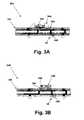
- an integrated circuit 30 A in accordance with an embodiment of the present inventionis depicted.
- An integrated circuit die 32 Ais attached to substrate 10 D using a bonding agent such as epoxy. While die 32 A is depicted as mounted above substrate 10 D, a die mounting recess may also be laser-ablated or otherwise provided in substrate 10 D, reducing the package height.
- a die mounting aperturemay be provided completely through thin-film dielectric layer 22 A in an area free of channels and vias, to reduce the package height by the thickness of thin film-dielectric layer 22 A.
- a cavity in prepared substrate 10may also be provided and aligned with an aperture in thin-film dielectric layer 22 A to further reduce package height.
- Electrical interconnects 34 A(wires) from die 32 A are wire bonded to the circuit pattern on the top side of substrate 10 D electrically connecting die 32 A to bonding areas 36 A providded by channel circuit patterns 29 A and/or vias 28 A.
- External terminals 38depicted as solder balls, are attached to BGA lands 36 B provided by channel circuit patterns 29 B and/or vias 28 B, providing a complete integrated circuit that may be encapsulated.
- Die 32 Bis a “flip-chip” die that is directly bonded to a substrate 10 E via solder balls 36 C. External solder ball terminals 38 are provided as in the embodiment of FIG. 3A .
- Substrate 10 Eis fabricated in the same manner as substrate 10 D, but may have a differing configuration to support the flip-chip die 32 B interconnect.
Landscapes
- Engineering & Computer Science (AREA)
- Microelectronics & Electronic Packaging (AREA)
- Manufacturing & Machinery (AREA)
- Ceramic Engineering (AREA)
- Physics & Mathematics (AREA)
- Condensed Matter Physics & Semiconductors (AREA)
- General Physics & Mathematics (AREA)
- Computer Hardware Design (AREA)
- Power Engineering (AREA)
- Electric Connection Of Electric Components To Printed Circuits (AREA)
- Production Of Multi-Layered Print Wiring Board (AREA)
Abstract
Description
Claims (18)
Priority Applications (1)
| Application Number | Priority Date | Filing Date | Title |
|---|---|---|---|
| US10/392,738US6930257B1 (en) | 2002-05-01 | 2003-03-19 | Integrated circuit substrate having laminated laser-embedded circuit layers |
Applications Claiming Priority (3)
| Application Number | Priority Date | Filing Date | Title |
|---|---|---|---|
| US10/138,225US6930256B1 (en) | 2002-05-01 | 2002-05-01 | Integrated circuit substrate having laser-embedded conductive patterns and method therefor |
| US26186802A | 2002-10-01 | 2002-10-01 | |
| US10/392,738US6930257B1 (en) | 2002-05-01 | 2003-03-19 | Integrated circuit substrate having laminated laser-embedded circuit layers |
Related Parent Applications (1)
| Application Number | Title | Priority Date | Filing Date |
|---|---|---|---|
| US10/138,225Continuation-In-PartUS6930256B1 (en) | 2001-06-19 | 2002-05-01 | Integrated circuit substrate having laser-embedded conductive patterns and method therefor |
Publications (1)
| Publication Number | Publication Date |
|---|---|
| US6930257B1true US6930257B1 (en) | 2005-08-16 |
Family
ID=34830043
Family Applications (2)
| Application Number | Title | Priority Date | Filing Date |
|---|---|---|---|
| US10/392,738Expired - LifetimeUS6930257B1 (en) | 2002-05-01 | 2003-03-19 | Integrated circuit substrate having laminated laser-embedded circuit layers |
| US11/527,104Expired - LifetimeUS7501338B1 (en) | 2001-06-19 | 2006-09-25 | Semiconductor package substrate fabrication method |
Family Applications After (1)
| Application Number | Title | Priority Date | Filing Date |
|---|---|---|---|
| US11/527,104Expired - LifetimeUS7501338B1 (en) | 2001-06-19 | 2006-09-25 | Semiconductor package substrate fabrication method |
Country Status (1)
| Country | Link |
|---|---|
| US (2) | US6930257B1 (en) |
Cited By (31)
| Publication number | Priority date | Publication date | Assignee | Title |
|---|---|---|---|---|
| US20050041398A1 (en)* | 2002-05-01 | 2005-02-24 | Huemoeller Ronald Patrick | Integrated circuit substrate having embedded back-side access conductors and vias |
| US20060067030A1 (en)* | 2004-09-28 | 2006-03-30 | Intel Corporation | Array capacitor with IC contacts and applications |
| US20070059917A1 (en)* | 2005-09-15 | 2007-03-15 | Samsung Electro-Mechanics Co., Ltd. | Printed circuit board having fine pattern and manufacturing method thereof |
| US20070163887A1 (en)* | 2004-01-29 | 2007-07-19 | Hofmann Hannes P | Method of manufacturing a circuit carrier and the use of the method |
| US7297562B1 (en) | 2002-05-01 | 2007-11-20 | Amkor Technology, Inc. | Circuit-on-foil process for manufacturing a laminated semiconductor package substrate having embedded conductive patterns |
| US20080043447A1 (en)* | 2002-05-01 | 2008-02-21 | Amkor Technology, Inc. | Semiconductor package having laser-embedded terminals |
| US7365006B1 (en) | 2004-05-05 | 2008-04-29 | Amkor Technology, Inc. | Semiconductor package and substrate having multi-level vias fabrication method |
| US20090109624A1 (en)* | 2007-10-25 | 2009-04-30 | Endicott Interconnect Technologies, Inc. | Circuitized substrate with internal cooling structure and electrical assembly utilizing same |
| US7589398B1 (en) | 2006-10-04 | 2009-09-15 | Amkor Technology, Inc. | Embedded metal features structure |
| US20100006334A1 (en)* | 2008-07-07 | 2010-01-14 | Ibiden Co., Ltd | Printed wiring board and method for manufacturing the same |
| US20100038124A1 (en)* | 2008-08-13 | 2010-02-18 | Yi-Chun Liu | Embedded structure and method for making the same |
| US7670962B2 (en) | 2002-05-01 | 2010-03-02 | Amkor Technology, Inc. | Substrate having stiffener fabrication method |
| US20100059866A1 (en)* | 2008-09-10 | 2010-03-11 | Stats Chippac, Ltd. | Semiconductor Device and Method of Forming Vertically Offset Bond on Trace Interconnects on Recessed and Raised Bond Fingers |
| US20100065324A1 (en)* | 2008-09-17 | 2010-03-18 | Yi-Chun Liu | Embedded structure and method for making the same |
| US7752752B1 (en) | 2007-01-09 | 2010-07-13 | Amkor Technology, Inc. | Method of fabricating an embedded circuit pattern |
| US20110147056A1 (en)* | 2009-12-17 | 2011-06-23 | Unimicron Technology Corp. | Circuit board and process for fabricating the same |
| US20110147339A1 (en)* | 2009-12-22 | 2011-06-23 | Unimicron Technology Corp. | Method for manufacturing wiring structure of wiring board |
| US20110147342A1 (en)* | 2009-12-22 | 2011-06-23 | Unimicron Technology Corp. | Method for fabricating wiring structure of wiring board |
| US20110155441A1 (en)* | 2009-12-31 | 2011-06-30 | Unimicron Technology Corp. | Circuit board and process for fabricating the same |
| US20110155440A1 (en)* | 2009-12-30 | 2011-06-30 | Unimicron Technology Corp. | Circuit board and process for manufacturing the same |
| US8288202B2 (en) | 2010-11-22 | 2012-10-16 | STATS ChiPAC, Ltd. | Method of forming partially-etched conductive layer recessed within substrate for bonding to semiconductor die |
| US8826531B1 (en) | 2005-04-05 | 2014-09-09 | Amkor Technology, Inc. | Method for making an integrated circuit substrate having laminated laser-embedded circuit layers |
| US8872329B1 (en) | 2009-01-09 | 2014-10-28 | Amkor Technology, Inc. | Extended landing pad substrate package structure and method |
| US20160234938A1 (en)* | 2013-09-18 | 2016-08-11 | Novalia Ltd | Circuit board assembly |
| US9812386B1 (en) | 2002-05-01 | 2017-11-07 | Amkor Technology, Inc. | Encapsulated semiconductor package |
| US10439272B1 (en) | 2015-11-23 | 2019-10-08 | Ethertronics, Inc. | Beam steering system configured for multi-client network |
| US10448518B2 (en) | 2015-06-02 | 2019-10-15 | Ethertronics, Inc. | Method for manufacturing a circuit having a lamination layer using laser direct structuring process |
| US10811277B2 (en) | 2004-03-23 | 2020-10-20 | Amkor Technology, Inc. | Encapsulated semiconductor package |
| US11081370B2 (en) | 2004-03-23 | 2021-08-03 | Amkor Technology Singapore Holding Pte. Ltd. | Methods of manufacturing an encapsulated semiconductor device |
| US11094560B1 (en) | 2004-03-23 | 2021-08-17 | Amkor Technology Singapore Holding Pte. Ltd. | Encapsulated semiconductor package |
| CN113573503A (en)* | 2021-07-28 | 2021-10-29 | 深圳市安元达电子有限公司 | Novel FPC precision bonding pad manufacturing method |
Families Citing this family (3)
| Publication number | Priority date | Publication date | Assignee | Title |
|---|---|---|---|---|
| US7750250B1 (en) | 2006-12-22 | 2010-07-06 | Amkor Technology, Inc. | Blind via capture pad structure |
| TWI384925B (en)* | 2009-03-17 | 2013-02-01 | Advanced Semiconductor Eng | Structure of embedded-trace substrate and method of manufacturing the same |
| CN111225517B (en)* | 2019-12-03 | 2021-03-09 | 厦门弘信电子科技集团股份有限公司 | Hole pattern electroplating method for FPC |
Citations (28)
| Publication number | Priority date | Publication date | Assignee | Title |
|---|---|---|---|---|
| US4322778A (en) | 1980-01-25 | 1982-03-30 | International Business Machines Corp. | High performance semiconductor package assembly |
| US4685033A (en) | 1984-08-28 | 1987-08-04 | Nec Corporation | Multilayer wiring substrate |
| US4706167A (en)* | 1983-11-10 | 1987-11-10 | Telemark Co., Inc. | Circuit wiring disposed on solder mask coating |
| US4811082A (en) | 1986-11-12 | 1989-03-07 | International Business Machines Corporation | High performance integrated circuit packaging structure |
| US5021047A (en) | 1989-08-29 | 1991-06-04 | Movern John B | Restricted use hypodermic syringe |
| US5072075A (en) | 1989-06-28 | 1991-12-10 | Digital Equipment Corporation | Double-sided hybrid high density circuit board and method of making same |
| US5110664A (en)* | 1989-07-10 | 1992-05-05 | Hitachi, Ltd. | Thick film and thin film composite substrate and electronic circuit apparatus using it |
| US5191174A (en) | 1990-08-01 | 1993-03-02 | International Business Machines Corporation | High density circuit board and method of making same |
| US5229550A (en) | 1990-10-30 | 1993-07-20 | International Business Machines Corporation | Encapsulated circuitized power core alignment and lamination |
| US5239448A (en) | 1991-10-28 | 1993-08-24 | International Business Machines Corporation | Formulation of multichip modules |
| US5371654A (en)* | 1992-10-19 | 1994-12-06 | International Business Machines Corporation | Three dimensional high performance interconnection package |
| US5404044A (en) | 1992-09-29 | 1995-04-04 | International Business Machines Corporation | Parallel process interposer (PPI) |
| US5508938A (en) | 1992-08-13 | 1996-04-16 | Fujitsu Limited | Special interconnect layer employing offset trace layout for advanced multi-chip module packages |
| US5582858A (en)* | 1991-10-07 | 1996-12-10 | International Business Machines Corporation | Adhesive layer in multi-level packaging and organic material as a metal diffusion barrier |
| US5774340A (en) | 1996-08-28 | 1998-06-30 | International Business Machines Corporation | Planar redistribution structure and printed wiring device |
| US5847453A (en) | 1996-03-27 | 1998-12-08 | Honda Giken Kogyo Kabushiki Kaisha | Microwave circuit package |
| US5936843A (en)* | 1997-10-14 | 1999-08-10 | Fujitsu Limited | Printed wiring board with mounted circuit element using a terminal density conversion board |
| US6081036A (en) | 1996-04-19 | 2000-06-27 | Matsushita Electronics Corp. | Semiconductor device |
| US6175087B1 (en) | 1998-12-02 | 2001-01-16 | International Business Machines Corporation | Composite laminate circuit structure and method of forming the same |
| US6204453B1 (en) | 1998-12-02 | 2001-03-20 | International Business Machines Corporation | Two signal one power plane circuit board |
| US6239485B1 (en) | 1998-11-13 | 2001-05-29 | Fujitsu Limited | Reduced cross-talk noise high density signal interposer with power and ground wrap |
| US6274821B1 (en)* | 1998-09-16 | 2001-08-14 | Denso Corporation | Shock-resistive printed circuit board and electronic device including the same |
| US6351031B1 (en) | 1999-10-12 | 2002-02-26 | Fujitsu Limited | Semiconductor device and method for manufacturing substrate of the same |
| US6365975B1 (en) | 1997-04-02 | 2002-04-02 | Tessera, Inc. | Chip with internal signal routing in external element |
| US6376906B1 (en) | 1997-02-12 | 2002-04-23 | Denso Corporation | Mounting structure of semiconductor element |
| US6479762B2 (en)* | 2000-11-20 | 2002-11-12 | Alps Electric Co., Ltd. | Printed circuit board having a pattern of traces formed by screen-printing |
| US6586682B2 (en)* | 2000-02-23 | 2003-07-01 | Kulicke & Soffa Holdings, Inc. | Printed wiring board with controlled line impedance |
| US6608757B1 (en) | 2002-03-18 | 2003-08-19 | International Business Machines Corporation | Method for making a printed wiring board |
Family Cites Families (94)
| Publication number | Priority date | Publication date | Assignee | Title |
|---|---|---|---|---|
| US3833838A (en) | 1972-11-13 | 1974-09-03 | A Christiansen | Electronic component mounting wafers for repeated connection in a variety of circuit designs |
| US3916434A (en) | 1972-11-30 | 1975-10-28 | Power Hybrids Inc | Hermetically sealed encapsulation of semiconductor devices |
| US3868724A (en) | 1973-11-21 | 1975-02-25 | Fairchild Camera Instr Co | Multi-layer connecting structures for packaging semiconductor devices mounted on a flexible carrier |
| CA1204213A (en) | 1982-09-09 | 1986-05-06 | Masahiro Takeda | Memory card having static electricity protection |
| US4642160A (en) | 1985-08-12 | 1987-02-10 | Interconnect Technology Inc. | Multilayer circuit board manufacturing |
| JPH0717175B2 (en) | 1985-08-20 | 1995-03-01 | 金井重要工業株式会社 | Automotive interior ceiling material for molding |
| US4716049A (en) | 1985-12-20 | 1987-12-29 | Hughes Aircraft Company | Compressive pedestal for microminiature connections |
| US4786952A (en) | 1986-07-24 | 1988-11-22 | General Motors Corporation | High voltage depletion mode MOS power field effect transistor |
| JPH0784115B2 (en) | 1987-03-31 | 1995-09-13 | 三菱電機株式会社 | Semiconductor device card |
| US4897338A (en) | 1987-08-03 | 1990-01-30 | Allied-Signal Inc. | Method for the manufacture of multilayer printed circuit boards |
| FR2637151A1 (en) | 1988-09-29 | 1990-03-30 | Commissariat Energie Atomique | METHOD OF MAKING ELECTRICAL CONNECTIONS THROUGH A SUBSTRATE |
| US4996391A (en) | 1988-09-30 | 1991-02-26 | Siemens Aktiengesellschaft | Printed circuit board having an injection molded substrate |
| JP2559834B2 (en) | 1989-01-12 | 1996-12-04 | 三菱電機株式会社 | IC card |
| US5108553A (en) | 1989-04-04 | 1992-04-28 | Olin Corporation | G-tab manufacturing process and the product produced thereby |
| US5081520A (en) | 1989-05-16 | 1992-01-14 | Minolta Camera Kabushiki Kaisha | Chip mounting substrate having an integral molded projection and conductive pattern |
| US5531020A (en) | 1989-11-14 | 1996-07-02 | Poly Flex Circuits, Inc. | Method of making subsurface electronic circuits |
| US5283459A (en) | 1989-11-15 | 1994-02-01 | Kabushiki Kaisha Toshiba | Semiconductor sensor including an aperture having a funnel shaped section intersecting a second section |
| WO1991014282A1 (en) | 1990-03-15 | 1991-09-19 | Fujitsu Limited | Semiconductor device having a plurality of chips |
| JP2890823B2 (en) | 1990-11-21 | 1999-05-17 | 株式会社デンソー | Display panel |
| US5379191A (en) | 1991-02-26 | 1995-01-03 | Microelectronics And Computer Technology Corporation | Compact adapter package providing peripheral to area translation for an integrated circuit chip |
| JPH05109975A (en) | 1991-10-14 | 1993-04-30 | Hitachi Ltd | Resin-sealed type semiconductor device |
| JPH05136323A (en) | 1991-11-13 | 1993-06-01 | Nec Corp | Integrated circuit device |
| FR2684235B1 (en) | 1991-11-25 | 1999-12-10 | Gemplus Card Int | INTEGRATED CIRCUIT CARD COMPRISING MEANS OF PROTECTING THE INTEGRATED CIRCUIT. |
| US5474958A (en) | 1993-05-04 | 1995-12-12 | Motorola, Inc. | Method for making semiconductor device having no die supporting surface |
| DE69432634D1 (en) | 1993-08-13 | 2003-06-12 | Irvine Sensors Corp | IC STACK AS REPLACEMENT FOR INDIVIDUAL IC |
| US5442852A (en) | 1993-10-26 | 1995-08-22 | Pacific Microelectronics Corporation | Method of fabricating solder ball array |
| US6042889A (en) | 1994-02-28 | 2000-03-28 | International Business Machines Corporation | Method for electrolessly depositing a metal onto a substrate using mediator ions |
| JPH07302318A (en) | 1994-03-09 | 1995-11-14 | Seiko Epson Corp | Card type electronic device |
| DE69527473T2 (en) | 1994-05-09 | 2003-03-20 | Nec Corp., Tokio/Tokyo | Semiconductor arrangement consisting of a semiconductor chip, which is connected by means of contact bumps on the printed circuit board, and assembly method |
| TW368745B (en) | 1994-08-15 | 1999-09-01 | Citizen Watch Co Ltd | Semiconductor device with IC chip highly secured |
| US6028364A (en) | 1994-09-20 | 2000-02-22 | Hitachi, Ltd. | Semiconductor device having a stress relieving mechanism |
| US5719749A (en) | 1994-09-26 | 1998-02-17 | Sheldahl, Inc. | Printed circuit assembly with fine pitch flexible printed circuit overlay mounted to printed circuit board |
| US5530288A (en) | 1994-10-12 | 1996-06-25 | International Business Machines Corporation | Passive interposer including at least one passive electronic component |
| JP3389357B2 (en) | 1994-11-29 | 2003-03-24 | 新光電気工業株式会社 | Substrate for mounting semiconductor chips |
| JPH08190615A (en) | 1995-01-09 | 1996-07-23 | Seiko Epson Corp | memory card |
| US5622588A (en) | 1995-02-02 | 1997-04-22 | Hestia Technologies, Inc. | Methods of making multi-tier laminate substrates for electronic device packaging |
| US6388203B1 (en) | 1995-04-04 | 2002-05-14 | Unitive International Limited | Controlled-shaped solder reservoirs for increasing the volume of solder bumps, and structures formed thereby |
| US5928767A (en) | 1995-06-07 | 1999-07-27 | Dexter Corporation | Conductive film composite |
| US5739581A (en) | 1995-11-17 | 1998-04-14 | National Semiconductor Corporation | High density integrated circuit package assembly with a heatsink between stacked dies |
| US5674785A (en) | 1995-11-27 | 1997-10-07 | Micron Technology, Inc. | Method of producing a single piece package for semiconductor die |
| US6013948A (en) | 1995-11-27 | 2000-01-11 | Micron Technology, Inc. | Stackable chip scale semiconductor package with mating contacts on opposed surfaces |
| US5826330A (en) | 1995-12-28 | 1998-10-27 | Hitachi Aic Inc. | Method of manufacturing multilayer printed wiring board |
| KR100216839B1 (en) | 1996-04-01 | 1999-09-01 | 김규현 | Solder Ball Land Metal Structure in BGA Semiconductor Package |
| JPH09327990A (en) | 1996-06-11 | 1997-12-22 | Toshiba Corp | Card storage |
| US5723907A (en) | 1996-06-25 | 1998-03-03 | Micron Technology, Inc. | Loc simm |
| US6405431B1 (en) | 1996-06-27 | 2002-06-18 | Samsung Electro-Mechanics Co., Ltd. | Method for manufacturing build-up multi-layer printed circuit board by using yag laser |
| DE19645854A1 (en) | 1996-11-07 | 1998-05-14 | Hewlett Packard Co | High structure density circuit board production |
| WO1998020528A1 (en) | 1996-11-08 | 1998-05-14 | W.L. Gore & Associates, Inc. | METHOD FOR IMPROVING RELIABILITY OF THIN CIRCUIT SUBSTRATES BY INCREASING THE Tg OF THE SUBSTRATE |
| WO1998020557A1 (en) | 1996-11-08 | 1998-05-14 | W.L. Gore & Associates, Inc. | Method for reducing via inductance in an electronic assembly and device |
| JP3266815B2 (en) | 1996-11-26 | 2002-03-18 | シャープ株式会社 | Method for manufacturing semiconductor integrated circuit device |
| US6064576A (en) | 1997-01-02 | 2000-05-16 | Texas Instruments Incorporated | Interposer having a cantilevered ball connection and being electrically connected to a printed circuit board |
| US5894108A (en) | 1997-02-11 | 1999-04-13 | National Semiconductor Corporation | Plastic package with exposed die |
| US6160705A (en) | 1997-05-09 | 2000-12-12 | Texas Instruments Incorporated | Ball grid array package and method using enhanced power and ground distribution circuitry |
| TW449844B (en) | 1997-05-17 | 2001-08-11 | Hyundai Electronics Ind | Ball grid array package having an integrated circuit chip |
| JPH10334205A (en) | 1997-05-30 | 1998-12-18 | Toshiba Corp | IC card and memory package |
| US5835355A (en) | 1997-09-22 | 1998-11-10 | Lsi Logic Corporation | Tape ball grid array package with perforated metal stiffener |
| US5952611A (en) | 1997-12-19 | 1999-09-14 | Texas Instruments Incorporated | Flexible pin location integrated circuit package |
| US6034427A (en) | 1998-01-28 | 2000-03-07 | Prolinx Labs Corporation | Ball grid array structure and method for packaging an integrated circuit chip |
| US6172419B1 (en) | 1998-02-24 | 2001-01-09 | Micron Technology, Inc. | Low profile ball grid array package |
| US6119338A (en) | 1998-03-19 | 2000-09-19 | Industrial Technology Research Institute | Method for manufacturing high-density multilayer printed circuit boards |
| USD445096S1 (en) | 1998-04-01 | 2001-07-17 | Sandisk Corporation | Removable memory card for use with portable electronic devices |
| US6184463B1 (en) | 1998-04-13 | 2001-02-06 | Harris Corporation | Integrated circuit package for flip chip |
| US5903052A (en) | 1998-05-12 | 1999-05-11 | Industrial Technology Research Institute | Structure for semiconductor package for improving the efficiency of spreading heat |
| US6280641B1 (en) | 1998-06-02 | 2001-08-28 | Mitsubishi Gas Chemical Company, Inc. | Printed wiring board having highly reliably via hole and process for forming via hole |
| EP1202348A3 (en) | 1998-06-04 | 2004-05-12 | Matsushita Electric Industrial Co., Ltd. | Semiconductor device and method of manufacturing same |
| US6040622A (en) | 1998-06-11 | 2000-03-21 | Sandisk Corporation | Semiconductor package using terminals formed on a conductive layer of a circuit board |
| JP2000031640A (en) | 1998-07-08 | 2000-01-28 | Ibiden Co Ltd | Printed wiring board and manufacture thereof |
| US6515355B1 (en) | 1998-09-02 | 2003-02-04 | Micron Technology, Inc. | Passivation layer for packaged integrated circuits |
| US6069407A (en) | 1998-11-18 | 2000-05-30 | Vlsi Technology, Inc. | BGA package using PCB and tape in a die-up configuration |
| US6392160B1 (en) | 1998-11-25 | 2002-05-21 | Lucent Technologies Inc. | Backplane for radio frequency signals |
| US6127833A (en) | 1999-01-04 | 2000-10-03 | Taiwan Semiconductor Manufacturing Co. | Test carrier for attaching a semiconductor device |
| TW411737B (en) | 1999-03-09 | 2000-11-11 | Unimicron Technology Corp | A 2-stage process to form micro via |
| JP3398721B2 (en) | 1999-05-20 | 2003-04-21 | アムコー テクノロジー コリア インコーポレーティド | Semiconductor package and manufacturing method thereof |
| TW443083B (en) | 1999-06-23 | 2001-06-23 | Asustek Comp Inc | Printed circuit board structure |
| US6122171A (en) | 1999-07-30 | 2000-09-19 | Micron Technology, Inc. | Heat sink chip package and method of making |
| USD446525S1 (en) | 1999-08-24 | 2001-08-14 | Kabushiki Kaisha Toshiba | IC memory card |
| US6517995B1 (en) | 1999-09-14 | 2003-02-11 | Massachusetts Institute Of Technology | Fabrication of finely featured devices by liquid embossing |
| US6803528B1 (en) | 1999-11-05 | 2004-10-12 | 3M Innovative Properties Company | Multi-layer double-sided wiring board and method of fabricating the same |
| US6497943B1 (en) | 2000-02-14 | 2002-12-24 | International Business Machines Corporation | Surface metal balancing to reduce chip carrier flexing |
| JP3677429B2 (en) | 2000-03-09 | 2005-08-03 | Necエレクトロニクス株式会社 | Method of manufacturing flip chip type semiconductor device |
| US6407341B1 (en) | 2000-04-25 | 2002-06-18 | International Business Machines Corporation | Conductive substructures of a multilayered laminate |
| US6667229B1 (en) | 2000-10-13 | 2003-12-23 | Bridge Semiconductor Corporation | Method of connecting a bumped compliant conductive trace and an insulative base to a semiconductor chip |
| US6548393B1 (en) | 2000-10-13 | 2003-04-15 | Charles W. C. Lin | Semiconductor chip assembly with hardened connection joint |
| US6699780B1 (en) | 2000-10-13 | 2004-03-02 | Bridge Semiconductor Corporation | Method of connecting a conductive trace to a semiconductor chip using plasma undercut etching |
| US6730857B2 (en) | 2001-03-13 | 2004-05-04 | International Business Machines Corporation | Structure having laser ablated features and method of fabricating |
| US6753612B2 (en) | 2001-04-05 | 2004-06-22 | International Business Machines Corporation | Economical high density chip carrier |
| US6815739B2 (en) | 2001-05-18 | 2004-11-09 | Corporation For National Research Initiatives | Radio frequency microelectromechanical systems (MEMS) devices on low-temperature co-fired ceramic (LTCC) substrates |
| US6815709B2 (en) | 2001-05-23 | 2004-11-09 | International Business Machines Corporation | Structure having flush circuitry features and method of making |
| US6660559B1 (en) | 2001-06-25 | 2003-12-09 | Amkor Technology, Inc. | Method of making a chip carrier package using laser ablation |
| US6534391B1 (en) | 2001-08-17 | 2003-03-18 | Amkor Technology, Inc. | Semiconductor package having substrate with laser-formed aperture through solder mask layer |
| US6759940B2 (en) | 2002-01-10 | 2004-07-06 | Lamina Ceramics, Inc. | Temperature compensating device with integral sheet thermistors |
| US6727645B2 (en) | 2002-05-24 | 2004-04-27 | International Business Machines Corporation | Organic LED device |
| US6787443B1 (en) | 2003-05-20 | 2004-09-07 | Intel Corporation | PCB design and method for providing vented blind vias |
| US7211289B2 (en) | 2003-12-18 | 2007-05-01 | Endicott Interconnect Technologies, Inc. | Method of making multilayered printed circuit board with filled conductive holes |
- 2003
- 2003-03-19USUS10/392,738patent/US6930257B1/ennot_activeExpired - Lifetime
- 2006
- 2006-09-25USUS11/527,104patent/US7501338B1/ennot_activeExpired - Lifetime
Patent Citations (28)
| Publication number | Priority date | Publication date | Assignee | Title |
|---|---|---|---|---|
| US4322778A (en) | 1980-01-25 | 1982-03-30 | International Business Machines Corp. | High performance semiconductor package assembly |
| US4706167A (en)* | 1983-11-10 | 1987-11-10 | Telemark Co., Inc. | Circuit wiring disposed on solder mask coating |
| US4685033A (en) | 1984-08-28 | 1987-08-04 | Nec Corporation | Multilayer wiring substrate |
| US4811082A (en) | 1986-11-12 | 1989-03-07 | International Business Machines Corporation | High performance integrated circuit packaging structure |
| US5072075A (en) | 1989-06-28 | 1991-12-10 | Digital Equipment Corporation | Double-sided hybrid high density circuit board and method of making same |
| US5110664A (en)* | 1989-07-10 | 1992-05-05 | Hitachi, Ltd. | Thick film and thin film composite substrate and electronic circuit apparatus using it |
| US5021047A (en) | 1989-08-29 | 1991-06-04 | Movern John B | Restricted use hypodermic syringe |
| US5191174A (en) | 1990-08-01 | 1993-03-02 | International Business Machines Corporation | High density circuit board and method of making same |
| US5229550A (en) | 1990-10-30 | 1993-07-20 | International Business Machines Corporation | Encapsulated circuitized power core alignment and lamination |
| US5582858A (en)* | 1991-10-07 | 1996-12-10 | International Business Machines Corporation | Adhesive layer in multi-level packaging and organic material as a metal diffusion barrier |
| US5239448A (en) | 1991-10-28 | 1993-08-24 | International Business Machines Corporation | Formulation of multichip modules |
| US5508938A (en) | 1992-08-13 | 1996-04-16 | Fujitsu Limited | Special interconnect layer employing offset trace layout for advanced multi-chip module packages |
| US5404044A (en) | 1992-09-29 | 1995-04-04 | International Business Machines Corporation | Parallel process interposer (PPI) |
| US5371654A (en)* | 1992-10-19 | 1994-12-06 | International Business Machines Corporation | Three dimensional high performance interconnection package |
| US5847453A (en) | 1996-03-27 | 1998-12-08 | Honda Giken Kogyo Kabushiki Kaisha | Microwave circuit package |
| US6081036A (en) | 1996-04-19 | 2000-06-27 | Matsushita Electronics Corp. | Semiconductor device |
| US5774340A (en) | 1996-08-28 | 1998-06-30 | International Business Machines Corporation | Planar redistribution structure and printed wiring device |
| US6376906B1 (en) | 1997-02-12 | 2002-04-23 | Denso Corporation | Mounting structure of semiconductor element |
| US6365975B1 (en) | 1997-04-02 | 2002-04-02 | Tessera, Inc. | Chip with internal signal routing in external element |
| US5936843A (en)* | 1997-10-14 | 1999-08-10 | Fujitsu Limited | Printed wiring board with mounted circuit element using a terminal density conversion board |
| US6274821B1 (en)* | 1998-09-16 | 2001-08-14 | Denso Corporation | Shock-resistive printed circuit board and electronic device including the same |
| US6239485B1 (en) | 1998-11-13 | 2001-05-29 | Fujitsu Limited | Reduced cross-talk noise high density signal interposer with power and ground wrap |
| US6175087B1 (en) | 1998-12-02 | 2001-01-16 | International Business Machines Corporation | Composite laminate circuit structure and method of forming the same |
| US6204453B1 (en) | 1998-12-02 | 2001-03-20 | International Business Machines Corporation | Two signal one power plane circuit board |
| US6351031B1 (en) | 1999-10-12 | 2002-02-26 | Fujitsu Limited | Semiconductor device and method for manufacturing substrate of the same |
| US6586682B2 (en)* | 2000-02-23 | 2003-07-01 | Kulicke & Soffa Holdings, Inc. | Printed wiring board with controlled line impedance |
| US6479762B2 (en)* | 2000-11-20 | 2002-11-12 | Alps Electric Co., Ltd. | Printed circuit board having a pattern of traces formed by screen-printing |
| US6608757B1 (en) | 2002-03-18 | 2003-08-19 | International Business Machines Corporation | Method for making a printed wiring board |
Non-Patent Citations (1)
| Title |
|---|
| NN 9311589 IBM Nov. 1, 1993. |
Cited By (62)
| Publication number | Priority date | Publication date | Assignee | Title |
|---|---|---|---|---|
| US9812386B1 (en) | 2002-05-01 | 2017-11-07 | Amkor Technology, Inc. | Encapsulated semiconductor package |
| US8322030B1 (en)* | 2002-05-01 | 2012-12-04 | Amkor Technology, Inc. | Circuit-on-foil process for manufacturing a laminated semiconductor package substrate having embedded conductive patterns |
| US20050041398A1 (en)* | 2002-05-01 | 2005-02-24 | Huemoeller Ronald Patrick | Integrated circuit substrate having embedded back-side access conductors and vias |
| US7399661B2 (en) | 2002-05-01 | 2008-07-15 | Amkor Technology, Inc. | Method for making an integrated circuit substrate having embedded back-side access conductors and vias |
| US10461006B1 (en) | 2002-05-01 | 2019-10-29 | Amkor Technology, Inc. | Encapsulated semiconductor package |
| US7297562B1 (en) | 2002-05-01 | 2007-11-20 | Amkor Technology, Inc. | Circuit-on-foil process for manufacturing a laminated semiconductor package substrate having embedded conductive patterns |
| US20080043447A1 (en)* | 2002-05-01 | 2008-02-21 | Amkor Technology, Inc. | Semiconductor package having laser-embedded terminals |
| US8316536B1 (en) | 2002-05-01 | 2012-11-27 | Amkor Technology, Inc. | Multi-level circuit substrate fabrication method |
| US7670962B2 (en) | 2002-05-01 | 2010-03-02 | Amkor Technology, Inc. | Substrate having stiffener fabrication method |
| US8927899B2 (en) | 2004-01-29 | 2015-01-06 | Atotech Deutschland Gmbh | Method of manufacturing a circuit carrier and the use of the method |
| US20070163887A1 (en)* | 2004-01-29 | 2007-07-19 | Hofmann Hannes P | Method of manufacturing a circuit carrier and the use of the method |
| US11081370B2 (en) | 2004-03-23 | 2021-08-03 | Amkor Technology Singapore Holding Pte. Ltd. | Methods of manufacturing an encapsulated semiconductor device |
| US10811277B2 (en) | 2004-03-23 | 2020-10-20 | Amkor Technology, Inc. | Encapsulated semiconductor package |
| US11094560B1 (en) | 2004-03-23 | 2021-08-17 | Amkor Technology Singapore Holding Pte. Ltd. | Encapsulated semiconductor package |
| US7365006B1 (en) | 2004-05-05 | 2008-04-29 | Amkor Technology, Inc. | Semiconductor package and substrate having multi-level vias fabrication method |
| US20060067030A1 (en)* | 2004-09-28 | 2006-03-30 | Intel Corporation | Array capacitor with IC contacts and applications |
| US7173804B2 (en)* | 2004-09-28 | 2007-02-06 | Intel Corporation | Array capacitor with IC contacts and applications |
| US8826531B1 (en) | 2005-04-05 | 2014-09-09 | Amkor Technology, Inc. | Method for making an integrated circuit substrate having laminated laser-embedded circuit layers |
| US20090229875A1 (en)* | 2005-09-15 | 2009-09-17 | Samsung Electro-Mechanics Co., Ltd. | Printed circuit board having fine pattern and manufacturing method thereof |
| US20070059917A1 (en)* | 2005-09-15 | 2007-03-15 | Samsung Electro-Mechanics Co., Ltd. | Printed circuit board having fine pattern and manufacturing method thereof |
| US11848214B2 (en) | 2006-08-01 | 2023-12-19 | Amkor Technology Singapore Holding Pte. Ltd. | Encapsulated semiconductor package |
| US7911037B1 (en) | 2006-10-04 | 2011-03-22 | Amkor Technology, Inc. | Method and structure for creating embedded metal features |
| US7589398B1 (en) | 2006-10-04 | 2009-09-15 | Amkor Technology, Inc. | Embedded metal features structure |
| US7752752B1 (en) | 2007-01-09 | 2010-07-13 | Amkor Technology, Inc. | Method of fabricating an embedded circuit pattern |
| US7738249B2 (en)* | 2007-10-25 | 2010-06-15 | Endicott Interconnect Technologies, Inc. | Circuitized substrate with internal cooling structure and electrical assembly utilizing same |
| US20090109624A1 (en)* | 2007-10-25 | 2009-04-30 | Endicott Interconnect Technologies, Inc. | Circuitized substrate with internal cooling structure and electrical assembly utilizing same |
| US20100006334A1 (en)* | 2008-07-07 | 2010-01-14 | Ibiden Co., Ltd | Printed wiring board and method for manufacturing the same |
| US20140116769A1 (en)* | 2008-07-07 | 2014-05-01 | Ibiden Co., Ltd. | Printed wiring board and method for manufacturing the same |
| US20100038124A1 (en)* | 2008-08-13 | 2010-02-18 | Yi-Chun Liu | Embedded structure and method for making the same |
| CN101652028B (en)* | 2008-08-13 | 2011-07-06 | 欣兴电子股份有限公司 | Embedded structure and method of forming same |
| US8132321B2 (en) | 2008-08-13 | 2012-03-13 | Unimicron Technology Corp. | Method for making embedded circuit structure |
| US8729397B2 (en) | 2008-08-13 | 2014-05-20 | Unimicron Technology Corp. | Embedded structure |
| US20100059866A1 (en)* | 2008-09-10 | 2010-03-11 | Stats Chippac, Ltd. | Semiconductor Device and Method of Forming Vertically Offset Bond on Trace Interconnects on Recessed and Raised Bond Fingers |
| US8169071B2 (en) | 2008-09-10 | 2012-05-01 | Stats Chippac, Ltd. | Semiconductor device having vertically offset bond on trace interconnects on recessed and raised bond fingers |
| US8742566B2 (en) | 2008-09-10 | 2014-06-03 | Stats Chippac, Ltd. | Semiconductor device having vertically offset bond on trace interconnects on recessed and raised bond fingers |
| US20110121452A1 (en)* | 2008-09-10 | 2011-05-26 | Stats Chippac, Ltd. | Semiconductor Device Having Vertically Offset Bond on Trace Interconnects on Recessed and Raised Bond Fingers |
| US7897502B2 (en)* | 2008-09-10 | 2011-03-01 | Stats Chippac, Ltd. | Method of forming vertically offset bond on trace interconnects on recessed and raised bond fingers |
| US8389398B2 (en) | 2008-09-10 | 2013-03-05 | Stats Chippac, Ltd. | Method of forming vertically offset bond on trace interconnects on recessed and raised bond fingers |
| US20100065324A1 (en)* | 2008-09-17 | 2010-03-18 | Yi-Chun Liu | Embedded structure and method for making the same |
| US8191248B2 (en) | 2008-09-17 | 2012-06-05 | Unimicron Technology Corp. | Method for making an embedded structure |
| US9462704B1 (en) | 2009-01-09 | 2016-10-04 | Amkor Technology, Inc. | Extended landing pad substrate package structure and method |
| US8872329B1 (en) | 2009-01-09 | 2014-10-28 | Amkor Technology, Inc. | Extended landing pad substrate package structure and method |
| US8294034B2 (en)* | 2009-12-17 | 2012-10-23 | Unimicron Technology Corp. | Circuit board and process for fabricating the same |
| US20110147056A1 (en)* | 2009-12-17 | 2011-06-23 | Unimicron Technology Corp. | Circuit board and process for fabricating the same |
| US8273651B2 (en) | 2009-12-22 | 2012-09-25 | Unimicron Technology Corp. | Method for fabricating wiring structure of wiring board |
| US8273256B2 (en) | 2009-12-22 | 2012-09-25 | Unimicron Technology Corp. | Method for manufacturing wiring structure of wiring board |
| US20110147339A1 (en)* | 2009-12-22 | 2011-06-23 | Unimicron Technology Corp. | Method for manufacturing wiring structure of wiring board |
| US20110147342A1 (en)* | 2009-12-22 | 2011-06-23 | Unimicron Technology Corp. | Method for fabricating wiring structure of wiring board |
| US8578600B2 (en) | 2009-12-30 | 2013-11-12 | Unimicron Technology Corp. | Process for manufacturing a circuit board |
| US20110155440A1 (en)* | 2009-12-30 | 2011-06-30 | Unimicron Technology Corp. | Circuit board and process for manufacturing the same |
| US8424202B2 (en) | 2009-12-31 | 2013-04-23 | Unimicron Technology Corp. | Process for fabricating a circuit board |
| US20110155441A1 (en)* | 2009-12-31 | 2011-06-30 | Unimicron Technology Corp. | Circuit board and process for fabricating the same |
| US8502392B2 (en) | 2010-11-22 | 2013-08-06 | Stats Chippac, Ltd. | Semiconductor device with partially-etched conductive layer recessed within substrate for bonding to semiconductor die |
| US8932908B2 (en) | 2010-11-22 | 2015-01-13 | Stats Chippac, Ltd. | Semiconductor device and method of forming partially-etched conductive layer recessed within substrate for bonding to semiconductor die |
| US8288202B2 (en) | 2010-11-22 | 2012-10-16 | STATS ChiPAC, Ltd. | Method of forming partially-etched conductive layer recessed within substrate for bonding to semiconductor die |
| US20160234938A1 (en)* | 2013-09-18 | 2016-08-11 | Novalia Ltd | Circuit board assembly |
| US10448518B2 (en) | 2015-06-02 | 2019-10-15 | Ethertronics, Inc. | Method for manufacturing a circuit having a lamination layer using laser direct structuring process |
| US11191165B2 (en) | 2015-06-02 | 2021-11-30 | Ethertronics, Inc. | Method for manufacturing a circuit having a lamination layer using laser direct structuring process |
| US11744022B2 (en) | 2015-06-02 | 2023-08-29 | KYOCERA AVX Components (San Diego), Inc. | Method for manufacturing a circuit having a lamination layer using laser direct structuring process |
| US11108136B2 (en) | 2015-11-23 | 2021-08-31 | Ethertronics, Inc. | Beam steering system configured for multi-client network |
| US10439272B1 (en) | 2015-11-23 | 2019-10-08 | Ethertronics, Inc. | Beam steering system configured for multi-client network |
| CN113573503A (en)* | 2021-07-28 | 2021-10-29 | 深圳市安元达电子有限公司 | Novel FPC precision bonding pad manufacturing method |
Also Published As
| Publication number | Publication date |
|---|---|
| US7501338B1 (en) | 2009-03-10 |
Similar Documents
| Publication | Publication Date | Title |
|---|---|---|
| US6930257B1 (en) | Integrated circuit substrate having laminated laser-embedded circuit layers | |
| US6930256B1 (en) | Integrated circuit substrate having laser-embedded conductive patterns and method therefor | |
| US7923367B2 (en) | Multilayer wiring substrate mounted with electronic component and method for manufacturing the same | |
| EP0526133B1 (en) | Polyimide multilayer wiring substrate and method for manufacturing the same | |
| US7738256B2 (en) | Multilayer substrate including components therein | |
| KR100395862B1 (en) | Flip chip type semiconductor device and method for manufacturing the same | |
| US6861284B2 (en) | Semiconductor device and production method thereof | |
| US6594891B1 (en) | Process for forming multi-layer electronic structures | |
| US7365006B1 (en) | Semiconductor package and substrate having multi-level vias fabrication method | |
| KR100763345B1 (en) | Manufacturing Method of Electronic Circuit Board | |
| US20080308308A1 (en) | Method of manufacturing wiring board, method of manufacturing semiconductor device and wiring board | |
| US7399661B2 (en) | Method for making an integrated circuit substrate having embedded back-side access conductors and vias | |
| US20090085192A1 (en) | Packaging substrate structure having semiconductor chip embedded therein and fabricating method thereof | |
| US6831371B1 (en) | Integrated circuit substrate having embedded wire conductors and method therefor | |
| KR100335454B1 (en) | Multilayered circuit board for semiconductor chip module, and method of manufacturing the same | |
| WO2000025558A1 (en) | A circuit board and a method for manufacturing the same | |
| US11160160B1 (en) | PCB for bare die mount and process therefore | |
| JP3577421B2 (en) | Package for semiconductor device | |
| JP4070470B2 (en) | Multilayer circuit board for semiconductor device, manufacturing method thereof, and semiconductor device | |
| JP2002313996A (en) | Substrate for semiconductor package, and its manufacturing method | |
| US8826531B1 (en) | Method for making an integrated circuit substrate having laminated laser-embedded circuit layers | |
| HK1040569A1 (en) | Improved integrated circuit structure | |
| US20080043447A1 (en) | Semiconductor package having laser-embedded terminals | |
| US6207354B1 (en) | Method of making an organic chip carrier package | |
| US20020063331A1 (en) | Film carrier semiconductor device |
Legal Events
| Date | Code | Title | Description |
|---|---|---|---|
| AS | Assignment | Owner name:AMKOR TECHNOLOGY, INC., ARIZONA Free format text:ASSIGNMENT OF ASSIGNORS INTEREST;ASSIGNORS:HINER, DAVID JON;HUEMOELLER, RONALD PATRICK;RUSLI, SUKIANTO;REEL/FRAME:013902/0864 Effective date:20030307 | |
| STCF | Information on status: patent grant | Free format text:PATENTED CASE | |
| AS | Assignment | Owner name:BANK OF AMERICA, N.A., TEXAS Free format text:SECURITY AGREEMENT;ASSIGNOR:AMKOR TECHNOLOGY, INC.;REEL/FRAME:017379/0630 Effective date:20051123 | |
| FPAY | Fee payment | Year of fee payment:4 | |
| FPAY | Fee payment | Year of fee payment:8 | |
| FPAY | Fee payment | Year of fee payment:12 | |
| AS | Assignment | Owner name:BANK OF AMERICA, N.A., AS AGENT, CALIFORNIA Free format text:SECURITY INTEREST;ASSIGNOR:AMKOR TECHNOLOGY, INC.;REEL/FRAME:046683/0139 Effective date:20180713 | |
| AS | Assignment | Owner name:AMKOR TECHNOLOGY SINGAPORE HOLDING PTE.LTD., SINGAPORE Free format text:ASSIGNMENT OF ASSIGNORS INTEREST;ASSIGNOR:AMKOR TECHNOLOGY, INC.;REEL/FRAME:054067/0135 Effective date:20191119 |