US6929762B2 - Method of reducing pattern distortions during imprint lithography processes - Google Patents
Method of reducing pattern distortions during imprint lithography processesDownload PDFInfo
- Publication number
- US6929762B2 US6929762B2US10/293,223US29322302AUS6929762B2US 6929762 B2US6929762 B2US 6929762B2US 29322302 AUS29322302 AUS 29322302AUS 6929762 B2US6929762 B2US 6929762B2
- Authority
- US
- United States
- Prior art keywords
- mold
- substrate
- pattern
- region
- layer
- Prior art date
- Legal status (The legal status is an assumption and is not a legal conclusion. Google has not performed a legal analysis and makes no representation as to the accuracy of the status listed.)
- Expired - Lifetime, expires
Links
Images


Classifications
- B—PERFORMING OPERATIONS; TRANSPORTING
- B82—NANOTECHNOLOGY
- B82Y—SPECIFIC USES OR APPLICATIONS OF NANOSTRUCTURES; MEASUREMENT OR ANALYSIS OF NANOSTRUCTURES; MANUFACTURE OR TREATMENT OF NANOSTRUCTURES
- B82Y10/00—Nanotechnology for information processing, storage or transmission, e.g. quantum computing or single electron logic
- B—PERFORMING OPERATIONS; TRANSPORTING
- B29—WORKING OF PLASTICS; WORKING OF SUBSTANCES IN A PLASTIC STATE IN GENERAL
- B29C—SHAPING OR JOINING OF PLASTICS; SHAPING OF MATERIAL IN A PLASTIC STATE, NOT OTHERWISE PROVIDED FOR; AFTER-TREATMENT OF THE SHAPED PRODUCTS, e.g. REPAIRING
- B29C59/00—Surface shaping of articles, e.g. embossing; Apparatus therefor
- B29C59/002—Component parts, details or accessories; Auxiliary operations
- B—PERFORMING OPERATIONS; TRANSPORTING
- B29—WORKING OF PLASTICS; WORKING OF SUBSTANCES IN A PLASTIC STATE IN GENERAL
- B29C—SHAPING OR JOINING OF PLASTICS; SHAPING OF MATERIAL IN A PLASTIC STATE, NOT OTHERWISE PROVIDED FOR; AFTER-TREATMENT OF THE SHAPED PRODUCTS, e.g. REPAIRING
- B29C59/00—Surface shaping of articles, e.g. embossing; Apparatus therefor
- B29C59/02—Surface shaping of articles, e.g. embossing; Apparatus therefor by mechanical means, e.g. pressing
- B29C59/022—Surface shaping of articles, e.g. embossing; Apparatus therefor by mechanical means, e.g. pressing characterised by the disposition or the configuration, e.g. dimensions, of the embossments or the shaping tools therefor
- B—PERFORMING OPERATIONS; TRANSPORTING
- B82—NANOTECHNOLOGY
- B82Y—SPECIFIC USES OR APPLICATIONS OF NANOSTRUCTURES; MEASUREMENT OR ANALYSIS OF NANOSTRUCTURES; MANUFACTURE OR TREATMENT OF NANOSTRUCTURES
- B82Y40/00—Manufacture or treatment of nanostructures
- G—PHYSICS
- G03—PHOTOGRAPHY; CINEMATOGRAPHY; ANALOGOUS TECHNIQUES USING WAVES OTHER THAN OPTICAL WAVES; ELECTROGRAPHY; HOLOGRAPHY
- G03F—PHOTOMECHANICAL PRODUCTION OF TEXTURED OR PATTERNED SURFACES, e.g. FOR PRINTING, FOR PROCESSING OF SEMICONDUCTOR DEVICES; MATERIALS THEREFOR; ORIGINALS THEREFOR; APPARATUS SPECIALLY ADAPTED THEREFOR
- G03F7/00—Photomechanical, e.g. photolithographic, production of textured or patterned surfaces, e.g. printing surfaces; Materials therefor, e.g. comprising photoresists; Apparatus specially adapted therefor
- G03F7/0002—Lithographic processes using patterning methods other than those involving the exposure to radiation, e.g. by stamping
- B—PERFORMING OPERATIONS; TRANSPORTING
- B29—WORKING OF PLASTICS; WORKING OF SUBSTANCES IN A PLASTIC STATE IN GENERAL
- B29C—SHAPING OR JOINING OF PLASTICS; SHAPING OF MATERIAL IN A PLASTIC STATE, NOT OTHERWISE PROVIDED FOR; AFTER-TREATMENT OF THE SHAPED PRODUCTS, e.g. REPAIRING
- B29C59/00—Surface shaping of articles, e.g. embossing; Apparatus therefor
- B29C59/02—Surface shaping of articles, e.g. embossing; Apparatus therefor by mechanical means, e.g. pressing
- B29C59/022—Surface shaping of articles, e.g. embossing; Apparatus therefor by mechanical means, e.g. pressing characterised by the disposition or the configuration, e.g. dimensions, of the embossments or the shaping tools therefor
- B29C2059/023—Microembossing
Definitions
- the field of inventionrelates generally to imprint lithography. More particularly, the present invention is directed to reducing pattern distortions during imprint lithography processes.
- Micro-fabricationinvolves the fabrication of very small structures, e.g., having features on the order of micro-meters or smaller.
- One area in which micro-fabrication has had a sizeable impactis in the processing of integrated circuits.
- micro-fabricationbecomes increasingly important.
- Micro-fabricationprovides greater process control while allowing increased reduction of the minimum feature dimension of the structures formed.
- Other areas of development in which micro-fabrication has been employedinclude biotechnology, optical technology, mechanical systems and the like.
- Willson et al.disclose a method of forming a relief image in a structure.
- the methodincludes providing a substrate having a transfer layer.
- the transfer layeris covered with a polymerizable fluid composition.
- a moldmakes mechanical contact with the polymerizable fluid.
- the moldincludes a relief structure, and the polymerizable fluid composition fills the relief structure.
- the polymerizable fluid compositionis then subjected to conditions to solidify and polymerize the same, forming a solidified polymeric material on the transfer layer that contains a relief structure complimentary to that of the mold.
- the moldis then separated from the solid polymeric material such that a replica of the relief structure in the mold is formed in the solidified polymeric material.
- the transfer layer and the solidified polymeric materialare subjected to an environment to selectively etch the transfer layer relative to the solidified polymeric material such that a relief image is formed in the transfer layer.
- the time required and the minimum feature dimension provided by this techniqueis dependent upon, inter alia, the composition of the polymerizable material.
- U.S. Pat. No. 5,772,905 to Choudiscloses a lithographic method and apparatus for creating ultra-fine (sub-25 nm) patterns in a thin film coated on a substrate in which a mold having at least one protruding feature is pressed into a thin film carried on a substrate.
- the protruding feature in the moldcreates a recess of the thin film.
- the moldis removed from the film.
- the thin filmthen is processed such that the thin film in the recess is removed exposing the underlying substrate.
- patterns in the moldare replaced in the thin film, completing the lithography.
- the patterns in the thin filmwill be, in subsequent processes, reproduced in the substrate or in another material which is added onto the substrate.
- LADIlaser assisted direct imprinting
- the present inventionis directed to a method of reducing distortions in a pattern disposed on a layer of a substrate, defining a recorded pattern, employing a mold having the pattern recorded therein, defining an original pattern.
- the methodincludes, defining a region on the layer in which to produce the recorded pattern. Relative extenuative variations between the substrate and the mold are created to ensure that the original pattern defines an area coextensive with the region. Thereafter, the recorded pattern is formed in the region.
- the relative extenuative variationsare created by heating or cooling of the substrate so that the region defines an area that is slightly smaller than the area of the original pattern. Then compression forces are applied to the mold to provide the recorded pattern with an area coextensive with the area of the region.
- the substratemay define an area slightly larger than the area of the region, and tensile forces are applied to the mold to make the area of the mold coextensive with the area of the region.
- the dimensions of the region and the recorded patternare determined by analyzing fiducial marks in the region and alignment marks on the mold.
- FIG. 1is a simplified elevation view of a lithographic system in accordance with the present invention
- FIG. 2is a simplified representation of material from which an imprinting layer, shown in FIG. 1 , is comprised before being polymerized and cross-linked;
- FIG. 3is a simplified representation of cross-linked polymer material into which the material shown in FIG. 2 is transformed after being subjected to radiation;
- FIG. 4is a simplified elevation view of a mold spaced-apart from the imprinting layer, shown in FIG. 1 , after patterning of the imprinting layer;
- FIG. 5is a simplified elevation view of an additional imprinting layer positioned atop of the substrate shown in FIG. 4 after the pattern in the first imprinting layer is transferred therein;
- FIG. 6is a top down view of a substrate, shown in FIGS. 1 , 2 and 5 , upon which imprinting layers are disposed;
- FIG. 7is a detailed view of FIG. 6 showing the position of the mold in one of the imprint regions
- FIG. 8is a flow diagram showing a method of reducing distortions in patterns formed using imprint lithography techniques in accordance with one embodiment of the present invention.
- FIG. 9is a flow diagram showing a method of reducing distortions in patterns formed using imprint lithography techniques in accordance with a second embodiment of the present invention.
- FIG. 10is a flow diagram showing a method of reducing distortions in patterns formed using imprint lithography techniques in accordance with a third embodiment of the present invention.
- FIG. 11is a flow diagram showing a method of reducing distortions in patterns formed using imprint lithography techniques in accordance with a fourth embodiment of the present invention.
- a lithographic systemin accordance with an embodiment of the present invention includes a substrate 10 having a substantially planar region shown as surface 12 . Disposed opposite substrate 10 is an imprint device, such as a mold 14 , having a plurality of features thereon, forming a plurality of spaced-apart recessions 16 and protrusions 18 .
- the plurality of featuresdefines an original pattern that is to be transferred into substrate 10 .
- recessions 16are a plurality of grooves extending along a direction parallel to protrusions 18 that provide a cross-section of mold 14 with a shape of a battlement.
- recessions 16may correspond to virtually any feature required to create an integrated circuit.
- a translation device 20is connected between mold 14 and substrate 10 to vary a distance “d” between mold 14 and substrate 10 .
- a radiation source 22is located so that mold 14 is positioned between radiation source 22 and substrate 10 . Radiation source 22 is configured to impinge actinic radiation on substrate 10 . To realize this, mold 14 is fabricated from material that allows it to be substantially transparent to the actinic radiation produced by radiation source 22 .
- a flowable regionsuch as an imprinting layer 24 , is disposed on surface 12 .
- Flowable regionmay be formed using any known technique such as a hot embossing process disclosed in U.S. Pat. No. 5,772,905, which is incorporated by reference in its entirety herein, or a laser assisted direct imprinting (LADI) process of the type described by Chou et al. in Ultrafast and Direct Imprint of Nanostructures in Silicon, Nature, Col. 417, pp. 835-837, June 2002.
- LADIlaser assisted direct imprinting
- flowable regionconsists of imprinting layer 24 being deposited as a plurality of spaced-apart discrete beads 25 of material 25 a on substrate 10 , discussed more fully below.
- Imprinting layer 24is formed from a material 25 a that may be selectively polymerized and cross-linked to record the original pattern therein, defining a recorded pattern.
- Material 25 ais shown in FIG. 3 as being cross-linked at points 25 b , forming cross-linked polymer material 25 c.
- the pattern recorded in imprinting layer 24is produced, in part, by mechanical contact with mold 14 .
- translation device 20reduces the distance “d” to allow imprinting layer 24 to come into mechanical contact with mold 14 , spreading beads 25 so as to form imprinting layer 24 with a contiguous formation of material 25 a over surface 12 .
- distance “d”is reduced to allow sub-portions 24 a of imprinting layer 24 to ingress into and fill recessions 16 .
- material 25 ais provided with the requisite properties to completely fill recessions 16 while covering surface 12 with a contiguous formation of material 25 a .
- sub-portions 24 a of imprinting layer 24 in superimposition with protrusions 18remain after the desired, usually minimum distance “d”, has been reached, leaving sub-portions 24 a with a thickness t 1 , and sub-portions 24 b with a thickness, t 2 .
- Thicknesses “t 1 ” and “t 2 ”may be any thickness desired, dependent upon the application.
- t 1is selected so as to be no greater than twice the width u of sub-portions 24 a , i.e., t 1 ⁇ 2u, shown more clearly in FIG. 4 .
- radiation source 22produces actinic radiation that polymerizes and cross-links material 25 a , forming cross-linked polymer material 25 c .
- the composition of imprinting layer 24transforms from material 25 a to material 25 c , which is a solid.
- material 25 cis solidified to provide side 24 c of imprinting layer 24 with a shape conforming to a shape of a surface 14 a of mold 14 , shown more clearly in FIG. 4 .
- an exemplary radiation source 22may produce ultraviolet radiation.
- Other radiation sourcesmay be employed, such as thermal, electromagnetic and the like.
- the selection of radiation employed to initiate the polymerization of the material in imprinting layer 24is known to one skilled in the art and typically depends on the specific application which is desired. After imprinting layer 24 is transformed to consist of material 25 c , translation device 20 increases the distance “d” so that mold 14 and imprinting layer 24 are spaced-apart.
- substrate 10 and imprinting layer 24may be etched to transfer the pattern on imprinting layer 24 into substrate 10 .
- the material from which imprinting layer 24 is formedmay be varied to define a relative etch rate with respect to substrate 10 , as desired.
- the relative etch rate of imprinting layer 24 to substrate 10may be in a range of about 1.5:1 to about 100:1.
- imprinting layer 24may be provided with an etch differential with respect to photo-resist material (not shown) selectively disposed on side 24 c .
- the photo-resist material(not shown) may be provided to further pattern imprinting layer 24 , using known techniques. Any etch process may be employed, dependent upon the etch rate desired and the underlying constituents that form substrate 10 and imprinting layer 24 . Exemplary etch processes may include plasma etching, reactive ion etching, chemical wet etching and the like.
- a problem addressed by the present inventionconcerns distortions in the pattern recorded into imprinting layer 24 due, inter alia, to extenuative variations of imprinting layer 24 and substrate 10 .
- These extenuative variationsmay be due, in part, to thermal fluctuations, such as differences in thermal coefficients of expansions between the materials in two or more layers; errors introduced by previous processes, such as, magnification errors, incorrect scanning speed; and errors introduced by environmental changes such as moisture content and barometric pressure changes.
- the extenuative variationsproduce what is commonly referred to as magnification/run-out errors.
- the magnification/run-out errorsoccur when a region of substrate 10 in which the original pattern is to be recorded exceeds the area of the original pattern.
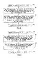
- a step-and-repeat processincludes defining a plurality of regions, shown as, a-l, on substrate 10 in which the original pattern on mold 14 will be recorded.
- the original pattern on mold 14may be coextensive with the entire surface of mold 14 , or simply located to a sub-portion thereof.
- the present inventionwill be discussed with respect to the original pattern being coextensive with the surface of mold 14 that faces substrate 10 .
- Proper execution of a step-and-repeat processmay include proper alignment of mold 14 with each of regions a-l. To that end, mold 14 includes alignment marks 114 a , shown as a “+” sign.
- One or more of regions a-lincludes fiducial marks 110 a .
- area-wise correction of magnification/run-out errorsis implemented by creating area-wise relative extenuative variations between mold 14 and substrate 10 .
- the temperature of substrate 10is varied so that one of regions a-l defines an area that is slightly less/greater than an area of the original pattern on mold 14 .
- the final compensation for magnification/run-out errorsis achieved by subjecting mold 14 to mechanical compression forces, shown by arrows F 1 and F 2 , orientated transversely to one another.
- One or more compression forces F 1 and F 2may be applied were the area of one of regions a-l slightly less than the area of the original pattern.
- one or more tensile forces F 1 ′ and F 2 ′may be be applied to mold 14 to stretch the same so that the original pattern is coextensive with one of regions a-l.
- tensile forces F 1 ′ and F 2 ′may be applied to mold 14 to stretch the same so that the original pattern is coextensive with one of regions a-l.
- the temperature of substrate 10is varied so that the distance along first and second directions that one of regions a-l extends changes. This may result in the distance that the one of regions a-l extends along a first direction, e.g., along the X-axis, being less than the distance that the original pattern on mold 14 extends.
- the distance that one of the regions a-l extends along a second direction, e.g., along the Y-axismay be coextensive with the distance that the original pattern on mold 14 extends along the second direction.
- an accurate measurement of substrate 10 in an X-Y planeis undertaken at step 200 .
- Thismay be achieved by sensing gross alignment fiducials 110 b present on substrate 10 using machine vision devices (not shown) and known signal processing techniques.
- the temperature of substrate 10may be varied, i.e., raised or lowered, so that the area of one of regions a-l is slightly less/greater than an area of the original pattern on mold 14 .
- the temperature variationsmay be achieved using a temperature controlled chuck or pedestal (not shown) against which substrate 10 rests.
- the area of each of regions a-lcan be determined by measurement of a change in distance between two collinear gross alignment fiducials 110 b.
- a change in the distance between two gross alignment fiducials 110 b collinear along one of the X or Y axesis determined. Thereafter, this change in distance is divided by a number of adjacent regions a-l on the substrate 10 along the X-axis. This provides the extenuative change of the areas of regions a-l attributable to extenuative changes in substrate 10 along the X-axis. If necessary the same measurement may be made to determine the change in area of regions a-l due to extenuative changes of substrate 10 along the Y-axis. However, it may also be assumed that the extenuative changes in substrate 10 may be uniform in the two orthogonal axes X and Y.
- compression forces, F 1 and F 2 , or tensile force F 1 ′ and F 2 ′are applied to mold 14 to establish the area of the original pattern to be coextensive with the area of one of the regions a-l in superimposition with the pattern.
- Thismay be achieved in real-time employing machine vision devices (not shown) and known signal processing techniques, to determine when two or more of alignment marks 114 a are aligned with two or more of fiducial marks 110 a , thereby ensuring proper scaling of mold 14 and substrate 10 .
- the original patternis recorded in the region a-l that is in superimposition with mold 14 , forming the recorded pattern.
- compression forces F 1 and F 2have the same magnitude, as the extenuative variations in either substrate 10 or mold 14 may not be uniform in all directions. Further, the magnification/run-out errors may not be identical in both X-Y directions. As a result, compression forces, F 1 and F 2 may differ to compensate for these anomalies. For similar reasons it is not necessary that tensile forces, F 1 ′ and F 2 ′ have the same magnitude, were these force employed. Furthermore, to ensure greater reduction in magnification/run-out errors, the extenuative variation in mold 14 may be undertaken after mold 14 contacts imprinting layer 124 , shown in FIG. 5 . However, this is not necessary.
- the area of the regions a-lshould be of appropriate dimensions to enable pattern on mold 14 to define an area coextensive therewith when mold 14 is subject to compression forces F 1 and F 2 , or tensile forces F 1 ′ and F 2 ′, without compromising the structural integrity of mold 14 .
- an accurate measurement of substrate 10 in an X-Y planeis undertaken at step 300 .
- compression forces, F 1 and F 2 , or tensile forces F 1 ′ and F 2 ′are applied to mold 14 to establish if the area of the original pattern is to be slightly less/greater than the area of one of the regions a-l in superimposition with the pattern.
- the temperature of substrate 10may be varied, i.e., raised or lowered, so that the area of one of regions a-l is coextensive with the area of the original pattern on mold 14 . The temperature variations may be achieved as discussed above.
- determination of whether the area of the original pattern on mold 14 is coextensive with one of the regions a-lmay be determined as discussed above with respect to FIG. 8 . Thereafter, at step 306 in FIG. 9 , after proper scaling is achieved so that magnification/run-out errors are reduced, if not vitiated, the original pattern is recorded in the region a-l that is in superimposition with mold 14 , shown in FIG. 1 .
- step 400accurate measurement of substrate 10 in an X-Y plane is undertaken at step 400 .
- step 402the dimensions of one of regions a-l in superimposition with mold 14 is determined. This may occur after the dimensions of substrate 10 have been varied, as discussed above. Alternatively, the dimensions of substrate 10 may be left unchanged, because either tensile forces, F 1 and F 2 ′, or compression forces, F 1 and F 2 , may be applied to substrate 10 , as necessary to properly scale mold 14 with substrate 10 to attenuate magnification/run-out errors.
- step 412it is determined whether there remain any regions a-l on substrate 10 in which to record the original pattern. If there are, the process proceeds to step 414 wherein mold 14 is placed in superimposition with the next region and the process proceeds to step 402 . Otherwise, the process ends at step 416 .
- step 404the process proceeds to step 406 wherein tensile forces F 1 ′ and F 2 ′, are applied to mold 14 causing expansion of the same.
- mold 14is heated at step 406 so that the pattern is coextensive with the area of region a-l in superimposition therewith. Then the process continues at step 412 .
- step 500accurate measurement of substrate 10 in an X-Y plane is undertaken at step 500 .
- step 502the dimensions of one of regions a-l in superimposition with mold 14 is determined.
- step 504it is determined whether the area of one of regions a-l in superimposition with mold 14 is larger than the area of pattern on mold 14 . If this is the case, the process proceeds to step 506 , otherwise the process proceeds to step 508 .
- step 508mold 14 is placed in contact with the region a-l in superimposition therewith, and the requisite magnitude of compression forces F 1 and F 2 is determined to apply to mold 14 to ensure that the area of pattern is coextensive with the area of this region a-l.
- step 510compression forces F 1 and F 2 are applied to mold 14 .
- mold 14is spaced-apart from the region a-l in superimposition with mold 14 and the process proceeds to step 512 where it is determined whether there remain any regions a-l on substrate 10 in which to record the original pattern. If there are, the process proceeds to step 514 wherein mold 14 is placed in superimposition with the next region and the process proceeds to step 502 . Otherwise, the process ends at step 516 .
- step 504the process proceeds to step 506 wherein the temperature of mold 14 is varied to cause expansion of the same.
- mold 14is heated at step 506 so that the pattern is slightly larger than the area of region a-l in superimposition therewith.
- step 508the process continues at step 508 .
- all of the magnification/run-out error correctionmay occur by compression of mold, without any need to vary the dimensions of substrate 10 .
- the present methodmay also be employed with extenuative variations to substrate 10 , as well.
Landscapes
- Engineering & Computer Science (AREA)
- Chemical & Material Sciences (AREA)
- Nanotechnology (AREA)
- Physics & Mathematics (AREA)
- General Physics & Mathematics (AREA)
- Crystallography & Structural Chemistry (AREA)
- Mechanical Engineering (AREA)
- Mathematical Physics (AREA)
- Theoretical Computer Science (AREA)
- Condensed Matter Physics & Semiconductors (AREA)
- Manufacturing & Machinery (AREA)
- Shaping Of Tube Ends By Bending Or Straightening (AREA)
Abstract
Description
Claims (20)
Priority Applications (1)
| Application Number | Priority Date | Filing Date | Title |
|---|---|---|---|
| US10/293,223US6929762B2 (en) | 2002-11-13 | 2002-11-13 | Method of reducing pattern distortions during imprint lithography processes |
Applications Claiming Priority (1)
| Application Number | Priority Date | Filing Date | Title |
|---|---|---|---|
| US10/293,223US6929762B2 (en) | 2002-11-13 | 2002-11-13 | Method of reducing pattern distortions during imprint lithography processes |
Publications (2)
| Publication Number | Publication Date |
|---|---|
| US20040089979A1 US20040089979A1 (en) | 2004-05-13 |
| US6929762B2true US6929762B2 (en) | 2005-08-16 |
Family
ID=32229627
Family Applications (1)
| Application Number | Title | Priority Date | Filing Date |
|---|---|---|---|
| US10/293,223Expired - LifetimeUS6929762B2 (en) | 2002-11-13 | 2002-11-13 | Method of reducing pattern distortions during imprint lithography processes |
Country Status (1)
| Country | Link |
|---|---|
| US (1) | US6929762B2 (en) |
Cited By (41)
| Publication number | Priority date | Publication date | Assignee | Title |
|---|---|---|---|---|
| US20040116548A1 (en)* | 2002-12-12 | 2004-06-17 | Molecular Imprints, Inc. | Compositions for dark-field polymerization and method of using the same for imprint lithography processes |
| US20040146792A1 (en)* | 2002-12-13 | 2004-07-29 | Molecular Imprints, Inc. | Magnification correction employing out-of-plane distortion of a substrate |
| US20050006343A1 (en)* | 2003-07-09 | 2005-01-13 | Molecular Imprints, Inc. | Systems for magnification and distortion correction for imprint lithography processes |
| US20050064344A1 (en)* | 2003-09-18 | 2005-03-24 | University Of Texas System Board Of Regents | Imprint lithography templates having alignment marks |
| US20050098534A1 (en)* | 2003-11-12 | 2005-05-12 | Molecular Imprints, Inc. | Formation of conductive templates employing indium tin oxide |
| US20050106321A1 (en)* | 2003-11-14 | 2005-05-19 | Molecular Imprints, Inc. | Dispense geometery to achieve high-speed filling and throughput |
| US20050118817A1 (en)* | 2003-11-14 | 2005-06-02 | Tdk Corporation | Resist pattern forming method, magnetic recording medium manufacturing method and magnetic head manufacturing method |
| US20050270312A1 (en)* | 2004-06-03 | 2005-12-08 | Molecular Imprints, Inc. | Fluid dispensing and drop-on-demand dispensing for nano-scale manufacturing |
| US20060001194A1 (en)* | 2004-06-03 | 2006-01-05 | Molecular Imprints, Inc. | System for varying dimensions of a substrate during nanoscale manufacturing |
| WO2005047975A3 (en)* | 2003-11-12 | 2006-02-02 | Molecular Imprints Inc | Dispense geometry and conductive template to achieve high-speed filling and throughput |
| US20060076717A1 (en)* | 2002-07-11 | 2006-04-13 | Molecular Imprints, Inc. | Step and repeat imprint lithography processes |
| US20060126058A1 (en)* | 2004-11-30 | 2006-06-15 | Molecular Imprints, Inc. | Interferometric analysis for the manufacture of nano-scale devices |
| US20060228635A1 (en)* | 2005-04-07 | 2006-10-12 | Suleski Thomas J | Method and apparatus for fabricating shaped structures and shaped structures including one- , two- or three-dimensional patterns incorporated therein |
| US20070145643A1 (en)* | 2005-12-23 | 2007-06-28 | Asml Netherlands B.V. | Alignment for imprint lithography |
| WO2007126702A1 (en)* | 2006-04-03 | 2007-11-08 | Molecular Imprints, Inc. | System to vary the dimensions of a thin template |
| US20070284779A1 (en)* | 2006-06-13 | 2007-12-13 | Wei Wu | Imprint lithography apparatus and methods |
| US20080145773A1 (en)* | 2006-10-10 | 2008-06-19 | Shih-Yuan Wang | Imprint lithography apparatus and methods |
| US20080153312A1 (en)* | 2004-02-18 | 2008-06-26 | Molecular Imprints, Inc. | Methods for Exposure for the Purpose of Thermal Management for Imprint Lithography Processes |
| US20080174046A1 (en)* | 2002-07-11 | 2008-07-24 | Molecular Imprints Inc. | Capillary Imprinting Technique |
| US20090026657A1 (en)* | 2007-07-20 | 2009-01-29 | Molecular Imprints, Inc. | Alignment System and Method for a Substrate in a Nano-Imprint Process |
| US20090047606A1 (en)* | 2007-08-14 | 2009-02-19 | Asml Netherlands B.V. | Lithography meandering order |
| US20090140445A1 (en)* | 2007-12-04 | 2009-06-04 | Molecular Imprints | High Throughput Imprint Based on Contact Line Motion Tracking Control |
| US20090243153A1 (en)* | 2008-04-01 | 2009-10-01 | Molecular Imprints, Inc. | Large Area Roll-To-Roll Imprint Lithography |
| US7630067B2 (en) | 2004-11-30 | 2009-12-08 | Molecular Imprints, Inc. | Interferometric analysis method for the manufacture of nano-scale devices |
| US7691313B2 (en) | 2002-11-13 | 2010-04-06 | Molecular Imprints, Inc. | Method for expelling gas positioned between a substrate and a mold |
| US20100102470A1 (en)* | 2008-10-27 | 2010-04-29 | Molecular Imprints, Inc. | Misalignment Management |
| US7785096B2 (en) | 2004-11-30 | 2010-08-31 | Molecular Imprints, Inc. | Enhanced multi channel alignment |
| US7785526B2 (en) | 2004-07-20 | 2010-08-31 | Molecular Imprints, Inc. | Imprint alignment method, system, and template |
| US20100237042A1 (en)* | 2009-03-23 | 2010-09-23 | Intevac, Inc. | Process for optimization of island to trench ratio in patterned media |
| JP2011049302A (en)* | 2009-08-26 | 2011-03-10 | Fujifilm Corp | Pattern transfer device and pattern forming method |
| US20110084417A1 (en)* | 2009-10-08 | 2011-04-14 | Molecular Imprints, Inc. | Large area linear array nanoimprinting |
| US20110105366A1 (en)* | 2007-06-18 | 2011-05-05 | Illumina, Inc. | Microfabrication methods for the optimal patterning of substrates |
| US8012395B2 (en) | 2006-04-18 | 2011-09-06 | Molecular Imprints, Inc. | Template having alignment marks formed of contrast material |
| US20120074605A1 (en)* | 2010-09-24 | 2012-03-29 | Kabushiki Kaisha Toshiba | Fine processing method, fine processing apparatus, and recording medium with fine processing program recorded thereon |
| US8211214B2 (en) | 2003-10-02 | 2012-07-03 | Molecular Imprints, Inc. | Single phase fluid imprint lithography method |
| US8470617B2 (en) | 2006-04-07 | 2013-06-25 | Qd Vision, Inc. | Composition including material, methods of depositing material, articles including same and systems for depositing material |
| US8703406B2 (en) | 2012-07-12 | 2014-04-22 | Transfer Devices Inc. | Method of forming large-area masters for replication of transfer lithography templates |
| US20150155339A1 (en)* | 2013-11-29 | 2015-06-04 | Tsinghua University | Method of making organic light emitting diode array |
| US9120149B2 (en) | 2006-06-24 | 2015-09-01 | Qd Vision, Inc. | Methods and articles including nanomaterial |
| US11017993B2 (en)* | 2017-03-16 | 2021-05-25 | Bruker Daltonik Gmbh | Separation of liquid in droplets and sedimented material enclosed therein |
| US12386255B1 (en)* | 2018-07-24 | 2025-08-12 | Magic Leap, Inc. | Eyepiece assembly adhesion using a zero residual layer region |
Families Citing this family (20)
| Publication number | Priority date | Publication date | Assignee | Title |
|---|---|---|---|---|
| AU2001273491A1 (en)* | 2000-07-16 | 2002-02-05 | Board Of Regents, The University Of Texas System | High-resolution overlay alignment methods and systems for imprint lithography |
| EP1352295B1 (en)* | 2000-10-12 | 2015-12-23 | Board of Regents, The University of Texas System | Template for room temperature, low pressure micro- and nano-imprint lithography |
| US8349241B2 (en) | 2002-10-04 | 2013-01-08 | Molecular Imprints, Inc. | Method to arrange features on a substrate to replicate features having minimal dimensional variability |
| US6929762B2 (en) | 2002-11-13 | 2005-08-16 | Molecular Imprints, Inc. | Method of reducing pattern distortions during imprint lithography processes |
| US6871558B2 (en)* | 2002-12-12 | 2005-03-29 | Molecular Imprints, Inc. | Method for determining characteristics of substrate employing fluid geometries |
| US7452574B2 (en)* | 2003-02-27 | 2008-11-18 | Molecular Imprints, Inc. | Method to reduce adhesion between a polymerizable layer and a substrate employing a fluorine-containing layer |
| US7122079B2 (en) | 2004-02-27 | 2006-10-17 | Molecular Imprints, Inc. | Composition for an etching mask comprising a silicon-containing material |
| US7157036B2 (en) | 2003-06-17 | 2007-01-02 | Molecular Imprints, Inc | Method to reduce adhesion between a conformable region and a pattern of a mold |
| US7136150B2 (en) | 2003-09-25 | 2006-11-14 | Molecular Imprints, Inc. | Imprint lithography template having opaque alignment marks |
| US8076386B2 (en) | 2004-02-23 | 2011-12-13 | Molecular Imprints, Inc. | Materials for imprint lithography |
| US20050276919A1 (en)* | 2004-06-01 | 2005-12-15 | Molecular Imprints, Inc. | Method for dispensing a fluid on a substrate |
| JP4742074B2 (en)* | 2007-06-29 | 2011-08-10 | 富士フイルム株式会社 | Method for manufacturing magnetic recording medium |
| KR100974603B1 (en)* | 2007-12-21 | 2010-08-06 | 연세대학교 산학협력단 | Magnetic pattern formation method and patterned media manufacturing method through magnetic pattern formation |
| WO2010021291A1 (en)* | 2008-08-22 | 2010-02-25 | コニカミノルタオプト株式会社 | Substrate manufacturing method, substrate manufactured by the substrate manufacturing method and magnetic recording medium using the substrate |
| JP2010278041A (en)* | 2009-05-26 | 2010-12-09 | Toshiba Corp | Method for forming imprint template and imprint method using this template |
| NL2005254A (en)* | 2009-09-22 | 2011-03-23 | Asml Netherlands Bv | Imprint lithography method and apparatus. |
| US20150140156A1 (en)* | 2013-11-20 | 2015-05-21 | Thomas W. Palone | Non-deformable patterned template |
| US9513543B2 (en)* | 2013-11-20 | 2016-12-06 | Eastman Kodak Company | Method for forming a non-deformable patterned template |
| DE102019104335B4 (en)* | 2019-02-20 | 2021-11-18 | Kunststoff-Institut Für Die Mittelständische Wirtschaft Nrw Gmbh (Kimw Nrw Gmbh) | Method for generating a surface structuring on the surface of a thermoplastic plastic body as well as plastic body produced therewith |
| JP7437928B2 (en)* | 2019-12-17 | 2024-02-26 | キヤノン株式会社 | Imprint equipment, imprint method, and article manufacturing method |
Citations (302)
| Publication number | Priority date | Publication date | Assignee | Title |
|---|---|---|---|---|
| US3527062A (en) | 1968-09-25 | 1970-09-08 | Singer General Precision | Universal joint flexure hinge |
| US3783520A (en) | 1970-09-28 | 1974-01-08 | Bell Telephone Labor Inc | High accuracy alignment procedure utilizing moire patterns |
| US3807029A (en) | 1972-09-05 | 1974-04-30 | Bendix Corp | Method of making a flexural pivot |
| US3807027A (en) | 1972-03-31 | 1974-04-30 | Johns Manville | Method of forming the bell end of a bell and spigot joint |
| US3811665A (en) | 1972-09-05 | 1974-05-21 | Bendix Corp | Flexural pivot with diaphragm means |
| US4062600A (en) | 1976-04-05 | 1977-12-13 | Litton Systems, Inc. | Dual-gimbal gyroscope flexure suspension |
| US4070116A (en) | 1975-06-23 | 1978-01-24 | International Business Machines Corporation | Gap measuring device for defining the distance between two or more surfaces |
| US4098001A (en) | 1976-10-13 | 1978-07-04 | The Charles Stark Draper Laboratory, Inc. | Remote center compliance system |
| DE2800476A1 (en) | 1977-01-07 | 1978-07-13 | Instruments Sa | Mass prodn. method for grids, graticules etc. - using revolving drum, belt carrying resin and UV light source for polymerisation process |
| US4119688A (en) | 1975-11-03 | 1978-10-10 | International Business Machines Corporation | Electro-lithography method |
| US4155169A (en) | 1978-03-16 | 1979-05-22 | The Charles Stark Draper Laboratory, Inc. | Compliant assembly system device |
| US4201800A (en) | 1978-04-28 | 1980-05-06 | International Business Machines Corp. | Hardened photoresist master image mask process |
| US4202107A (en) | 1978-10-23 | 1980-05-13 | Watson Paul C | Remote axis admittance system |
| JPS5588332A (en) | 1978-12-26 | 1980-07-04 | Fujitsu Ltd | Method of mask alignment |
| US4256829A (en)* | 1977-05-11 | 1981-03-17 | U.S. Philips Corporation | Method of manufacturing solid-state devices in which planar dimensional distortion is reduced |
| US4267212A (en) | 1978-09-20 | 1981-05-12 | Fuji Photo Film Co., Ltd. | Spin coating process |
| JPS577931A (en) | 1980-06-18 | 1982-01-16 | Toshiba Corp | Method for measuring gap |
| US4326805A (en) | 1980-04-11 | 1982-04-27 | Bell Telephone Laboratories, Incorporated | Method and apparatus for aligning mask and wafer members |
| US4337579A (en) | 1980-04-16 | 1982-07-06 | The Charles Stark Draper Laboratory, Inc. | Deformable remote center compliance device |
| US4355469A (en) | 1980-11-28 | 1982-10-26 | The Charles Stark Draper Laboratory, Inc. | Folded remote center compliance device |
| JPS58129074A (en) | 1982-01-27 | 1983-08-01 | Dainippon Printing Co Ltd | Ink composition for forming thermal transfer layer |
| US4414750A (en) | 1981-10-19 | 1983-11-15 | The Charles Stark Draper Laboratory, Inc. | Single stage remote center compliance device |
| US4426247A (en) | 1982-04-12 | 1984-01-17 | Nippon Telegraph & Telephone Public Corporation | Method for forming micropattern |
| US4440804A (en) | 1982-08-02 | 1984-04-03 | Fairchild Camera & Instrument Corporation | Lift-off process for fabricating self-aligned contacts |
| US4451507A (en) | 1982-10-29 | 1984-05-29 | Rca Corporation | Automatic liquid dispensing apparatus for spinning surface of uniform thickness |
| US4507331A (en) | 1983-12-12 | 1985-03-26 | International Business Machines Corporation | Dry process for forming positive tone micro patterns |
| US4544572A (en) | 1982-09-07 | 1985-10-01 | Minnesota Mining And Manufacturing Company | Coated ophthalmic lenses and method for coating the same |
| US4552833A (en) | 1984-05-14 | 1985-11-12 | International Business Machines Corporation | Radiation sensitive and oxygen plasma developable resist |
| US4552832A (en) | 1982-03-06 | 1985-11-12 | Braun Aktiengesellschaft | Shear foil having protrusions on its skin-contacting surface thereof |
| US4600309A (en) | 1982-12-30 | 1986-07-15 | Thomson-Csf | Process and apparatus for theoptical alignment of patterns in two close-up planes in an exposure means incorporating a divergent radiation source |
| US4610442A (en) | 1982-10-19 | 1986-09-09 | Matsushita Electric Industrial Co, Ltd. | Positioning table |
| US4657845A (en) | 1986-01-14 | 1987-04-14 | International Business Machines Corporation | Positive tone oxygen plasma developable photoresist |
| WO1987002935A1 (en) | 1985-11-18 | 1987-05-21 | Eastman Kodak Company | Process for making optical recording media |
| US4692205A (en) | 1986-01-31 | 1987-09-08 | International Business Machines Corporation | Silicon-containing polyimides as oxygen etch stop and dual dielectric coatings |
| US4694703A (en) | 1984-06-28 | 1987-09-22 | Lear Siegler, Inc. | Circumferentially oriented flexure suspension |
| EP0244884A1 (en) | 1986-03-28 | 1987-11-11 | Koninklijke Philips Electronics N.V. | Method of providing a mould with a release layer |
| US4707218A (en) | 1986-10-28 | 1987-11-17 | International Business Machines Corporation | Lithographic image size reduction |
| US4724222A (en) | 1986-04-28 | 1988-02-09 | American Telephone And Telegraph Company, At&T Bell Laboratories | Wafer chuck comprising a curved reference surface |
| US4731155A (en) | 1987-04-15 | 1988-03-15 | General Electric Company | Process for forming a lithographic mask |
| US4737425A (en) | 1986-06-10 | 1988-04-12 | International Business Machines Corporation | Patterned resist and process |
| JPS63138730A (en) | 1986-12-01 | 1988-06-10 | Canon Inc | Gap alignment device |
| US4763886A (en) | 1986-12-26 | 1988-08-16 | Nippon Thompson Co., Ltd. | XY-positioning table |
| US4772878A (en) | 1987-05-06 | 1988-09-20 | Kane Roger A | Merchandise theft deterrent sensor |
| US4808511A (en) | 1987-05-19 | 1989-02-28 | International Business Machines Corporation | Vapor phase photoresist silylation process |
| US4826943A (en) | 1986-07-25 | 1989-05-02 | Oki Electric Industry Co., Ltd. | Negative resist material |
| US4846931A (en) | 1988-03-29 | 1989-07-11 | Bell Communications Research, Inc. | Method for lifting-off epitaxial films |
| US4848179A (en) | 1988-02-16 | 1989-07-18 | Trw Inc. | Flexidigit robotic manipulator |
| US4848911A (en) | 1986-06-11 | 1989-07-18 | Kabushiki Kaisha Toshiba | Method for aligning first and second objects, relative to each other, and apparatus for practicing this method |
| JPH01196749A (en) | 1988-01-30 | 1989-08-08 | Hoya Corp | Manufacture of substrate for optical information recording medium |
| US4857477A (en) | 1986-09-18 | 1989-08-15 | Oki Electric Industry Co., Ltd. | Process for fabricating a semiconductor device |
| US4883561A (en) | 1988-03-29 | 1989-11-28 | Bell Communications Research, Inc. | Lift-off and subsequent bonding of epitaxial films |
| US4887283A (en) | 1988-09-27 | 1989-12-12 | Mitsubishi Denki Kabushiki Kaisha | X-ray mask and exposure method employing the same |
| US4891303A (en) | 1988-05-26 | 1990-01-02 | Texas Instruments Incorporated | Trilayer microlithographic process using a silicon-based resist as the middle layer |
| JPH0224848A (en) | 1988-07-14 | 1990-01-26 | Canon Inc | Production of substrate for optical recording medium |
| US4908298A (en) | 1985-03-19 | 1990-03-13 | International Business Machines Corporation | Method of creating patterned multilayer films for use in production of semiconductor circuits and systems |
| US4909151A (en) | 1986-11-10 | 1990-03-20 | Matsushita Electric Industrial Co., Ltd. | Method of forming an ink image and printing the formed image |
| JPH0292603A (en) | 1988-09-30 | 1990-04-03 | Hoya Corp | Manufacture of data recording board with guide groove |
| US4919748A (en) | 1989-06-30 | 1990-04-24 | At&T Bell Laboratories | Method for tapered etching |
| US4921778A (en) | 1988-07-29 | 1990-05-01 | Shipley Company Inc. | Photoresist pattern fabrication employing chemically amplified metalized material |
| US4929083A (en) | 1986-06-19 | 1990-05-29 | Xerox Corporation | Focus and overlay characterization and optimization for photolithographic exposure |
| US4931351A (en) | 1987-01-12 | 1990-06-05 | Eastman Kodak Company | Bilayer lithographic process |
| JPH02192045A (en) | 1989-01-20 | 1990-07-27 | Fujitsu Ltd | Production of optical disk substrate |
| US4959252A (en) | 1986-09-29 | 1990-09-25 | Rhone-Poulenc Chimie | Highly oriented thermotropic optical disc member |
| US4964145A (en) | 1989-07-24 | 1990-10-16 | International Business Machines Corporation | System for magnification correction of conductive X-ray lithography mask substrates |
| US4964945A (en) | 1988-12-09 | 1990-10-23 | Minnesota Mining And Manufacturing Company | Lift off patterning process on a flexible substrate |
| US4976818A (en) | 1987-10-26 | 1990-12-11 | Matsushita Electric Industrial Co., Ltd. | Fine pattern forming method |
| US4980316A (en) | 1988-07-20 | 1990-12-25 | Siemens Aktiengesellschaft | Method for producing a resist structure on a semiconductor |
| US4999280A (en) | 1989-03-17 | 1991-03-12 | International Business Machines Corporation | Spray silylation of photoresist images |
| US5053318A (en) | 1989-05-18 | 1991-10-01 | Shipley Company Inc. | Plasma processing with metal mask integration |
| US5063321A (en) | 1988-02-24 | 1991-11-05 | Teldix Gmbh | Torsional vibration drive |
| US5071694A (en) | 1989-02-21 | 1991-12-10 | Kanegafuchi Kagaku Kogyo Kabushiki Kaisha | Multi-layer resist |
| US5072126A (en) | 1990-10-31 | 1991-12-10 | International Business Machines Corporation | Promixity alignment using polarized illumination and double conjugate projection lens |
| US5073230A (en) | 1990-04-17 | 1991-12-17 | Arizona Board Of Regents Acting On Behalf Of Arizona State University | Means and methods of lifting and relocating an epitaxial device layer |
| US5074667A (en) | 1988-08-15 | 1991-12-24 | Sumitomo Heavy Industries Co. Ltd. | Position detector employing a sector fresnel zone plate |
| JPH0470379A (en) | 1990-07-03 | 1992-03-05 | Oki Electric Ind Co Ltd | Manufacture of master printing plate |
| US5108875A (en) | 1988-07-29 | 1992-04-28 | Shipley Company Inc. | Photoresist pattern fabrication employing chemically amplified metalized material |
| US5110514A (en) | 1989-05-01 | 1992-05-05 | Soane Technologies, Inc. | Controlled casting of a shrinkable material |
| US5126006A (en) | 1990-10-30 | 1992-06-30 | International Business Machines Corp. | Plural level chip masking |
| US5148036A (en) | 1989-07-18 | 1992-09-15 | Canon Kabushiki Kaisha | Multi-axis wafer position detecting system using a mark having optical power |
| US5148037A (en) | 1988-09-09 | 1992-09-15 | Canon Kabushiki Kaisha | Position detecting method and apparatus |
| US5151754A (en) | 1989-10-06 | 1992-09-29 | Kabushiki Kaisha Toshiba | Method and an apparatus for measuring a displacement between two objects and a method and an apparatus for measuring a gap distance between two objects |
| US5155749A (en) | 1991-03-28 | 1992-10-13 | International Business Machines Corporation | Variable magnification mask for X-ray lithography |
| WO1992017883A1 (en) | 1991-03-26 | 1992-10-15 | Lennart Olsson | A method and a device for altering of the angular velocity of a driven rotating media carrier |
| US5169494A (en) | 1989-03-27 | 1992-12-08 | Matsushita Electric Industrial Co., Ltd. | Fine pattern forming method |
| US5171490A (en) | 1988-11-29 | 1992-12-15 | Fudim Efrem V | Method and apparatus for production of three-dimensional objects by irradiation of photopolymers |
| US5173393A (en) | 1989-04-24 | 1992-12-22 | Siemens Aktiengesellschaft | Etch-resistant deep ultraviolet resist process having an aromatic treating step after development |
| US5179863A (en) | 1990-03-05 | 1993-01-19 | Kabushiki Kaisha Toshiba | Method and apparatus for setting the gap distance between a mask and a wafer at a predetermined distance |
| US5198326A (en) | 1990-05-24 | 1993-03-30 | Matsushita Electric Industrial Co., Ltd. | Process for forming fine pattern |
| US5204739A (en) | 1992-02-07 | 1993-04-20 | Karl Suss America, Inc. | Proximity mask alignment using a stored video image |
| US5206983A (en) | 1991-06-24 | 1993-05-04 | Wisconsin Alumni Research Foundation | Method of manufacturing micromechanical devices |
| US5212147A (en) | 1991-05-15 | 1993-05-18 | Hewlett-Packard Company | Method of forming a patterned in-situ high Tc superconductive film |
| US5218193A (en) | 1991-02-16 | 1993-06-08 | Sumitomo Heavy Industries Co., Ltd. | Double-focus measurement apparatus utilizing chromatic aberration by having first and second bodies illuminated respectively by a single wavelength ray and a ray having a plurality of wavelengths |
| US5234793A (en) | 1989-04-24 | 1993-08-10 | Siemens Aktiengesellschaft | Method for dimensionally accurate structure transfer in bilayer technique wherein a treating step with a bulging agent is employed after development |
| US5240878A (en) | 1991-04-26 | 1993-08-31 | International Business Machines Corporation | Method for forming patterned films on a substrate |
| US5240550A (en) | 1990-09-21 | 1993-08-31 | U.S. Philips Corp. | Method of forming at least one groove in a substrate layer |
| US5242711A (en) | 1991-08-16 | 1993-09-07 | Rockwell International Corp. | Nucleation control of diamond films by microlithographic patterning |
| US5244818A (en) | 1992-04-08 | 1993-09-14 | Georgia Tech Research Corporation | Processes for lift-off of thin film materials and for the fabrication of three dimensional integrated circuits |
| US5259926A (en) | 1991-09-24 | 1993-11-09 | Hitachi, Ltd. | Method of manufacturing a thin-film pattern on a substrate |
| US5270984A (en) | 1991-08-26 | 1993-12-14 | Nec Corporation | Displacement amplification mechanism for piezoelectric elements |
| US5277749A (en) | 1991-10-17 | 1994-01-11 | International Business Machines Corporation | Methods and apparatus for relieving stress and resisting stencil delamination when performing lift-off processes that utilize high stress metals and/or multiple evaporation steps |
| US5314772A (en) | 1990-10-09 | 1994-05-24 | Arizona Board Of Regents | High resolution, multi-layer resist for microlithography and method therefor |
| US5318870A (en) | 1989-10-18 | 1994-06-07 | Massachusetts Institute Of Technology | Method of patterning a phenolic polymer film without photoactive additive through exposure to high energy radiation below 225 nm with subsequent organometallic treatment and the associated imaged article |
| US5324683A (en) | 1993-06-02 | 1994-06-28 | Motorola, Inc. | Method of forming a semiconductor structure having an air region |
| US5328810A (en) | 1990-05-07 | 1994-07-12 | Micron Technology, Inc. | Method for reducing, by a factor or 2-N, the minimum masking pitch of a photolithographic process |
| US5330881A (en) | 1989-06-02 | 1994-07-19 | Digital Equipment Corp. | Microlithographic method for producing thick, vertically-walled photoresist patterns |
| US5348616A (en) | 1993-05-03 | 1994-09-20 | Motorola, Inc. | Method for patterning a mold |
| US5355219A (en) | 1992-12-18 | 1994-10-11 | Matsushita Electric Industrial Co., Ltd. | Gap control apparatus and method utilizing heterodyne signal phase difference detection |
| US5357122A (en) | 1991-09-05 | 1994-10-18 | Sony Corporation | Three-dimensional optical-electronic integrated circuit device with raised sections |
| US5362606A (en) | 1989-10-18 | 1994-11-08 | Massachusetts Institute Of Technology | Positive resist pattern formation through focused ion beam exposure and surface barrier silylation |
| US5366851A (en) | 1991-07-23 | 1994-11-22 | At&T Bell Laboratories | Device fabrication process |
| US5374454A (en) | 1990-09-18 | 1994-12-20 | International Business Machines Incorporated | Method for conditioning halogenated polymeric materials and structures fabricated therewith |
| US5376810A (en) | 1992-06-26 | 1994-12-27 | California Institute Of Technology | Growth of delta-doped layers on silicon CCD/S for enhanced ultraviolet response |
| US5380474A (en) | 1993-05-20 | 1995-01-10 | Sandia Corporation | Methods for patterned deposition on a substrate |
| US5392123A (en) | 1991-09-06 | 1995-02-21 | Eastman Kodak Company | Optical monitor for measuring a gap between two rollers |
| US5414514A (en) | 1993-06-01 | 1995-05-09 | Massachusetts Institute Of Technology | On-axis interferometric alignment of plates using the spatial phase of interference patterns |
| US5417802A (en) | 1994-03-18 | 1995-05-23 | At&T Corp. | Integrated circuit manufacturing |
| US5422295A (en) | 1992-12-10 | 1995-06-06 | Samsung Electronics Co., Ltd. | Method for forming a semiconductor memory device having a vertical multi-layered storage electrode |
| US5421981A (en) | 1991-06-26 | 1995-06-06 | Ppg Industries, Inc. | Electrochemical sensor storage device |
| US5424549A (en) | 1991-12-20 | 1995-06-13 | Board Of Supervisors Of Louisiana State University And Agricultural And Mechanical College | Scanning systems for high resolution e-beam and X-ray lithography |
| US5425964A (en) | 1994-07-22 | 1995-06-20 | Rockwell International Corporation | Deposition of multiple layer thin films using a broadband spectral monitor |
| US5425848A (en) | 1993-03-16 | 1995-06-20 | U.S. Philips Corporation | Method of providing a patterned relief of cured photoresist on a flat substrate surface and device for carrying out such a method |
| US5431777A (en) | 1992-09-17 | 1995-07-11 | International Business Machines Corporation | Methods and compositions for the selective etching of silicon |
| US5439766A (en) | 1988-12-30 | 1995-08-08 | International Business Machines Corporation | Composition for photo imaging |
| US5452090A (en) | 1992-04-29 | 1995-09-19 | International Business Machines Corporation | CCD based confocal filtering for improved accuracy in x-ray proximity alignment |
| US5453157A (en) | 1994-05-16 | 1995-09-26 | Texas Instruments Incorporated | Low temperature anisotropic ashing of resist for semiconductor fabrication |
| US5458520A (en) | 1994-12-13 | 1995-10-17 | International Business Machines Corporation | Method for producing planar field emission structure |
| US5468542A (en) | 1985-12-23 | 1995-11-21 | General Electric Company | Method for production of a coated substrate with controlled surface characteristics |
| US5480047A (en) | 1993-06-04 | 1996-01-02 | Sharp Kabushiki Kaisha | Method for forming a fine resist pattern |
| US5504793A (en) | 1995-02-17 | 1996-04-02 | Loral Federal Systems Company | Magnification correction for 1-X proximity X-Ray lithography |
| US5507411A (en) | 1990-02-09 | 1996-04-16 | Berg Company, A Division Of Dec International, Inc. | Electronic dispensing heads |
| US5508527A (en) | 1992-01-31 | 1996-04-16 | Canon Kabushiki Kaisha | Method of detecting positional displacement between mask and wafer, and exposure apparatus adopting the method |
| US5512131A (en) | 1993-10-04 | 1996-04-30 | President And Fellows Of Harvard College | Formation of microstamped patterns on surfaces and derivative articles |
| US5515167A (en) | 1994-09-13 | 1996-05-07 | Hughes Aircraft Company | Transparent optical chuck incorporating optical monitoring |
| US5523878A (en) | 1994-06-30 | 1996-06-04 | Texas Instruments Incorporated | Self-assembled monolayer coating for micro-mechanical devices |
| US5545367A (en) | 1992-04-15 | 1996-08-13 | Soane Technologies, Inc. | Rapid prototype three dimensional stereolithography |
| EP0733455A2 (en) | 1995-03-22 | 1996-09-25 | IMM INSTITUT FÜR MIKROTECHNIK GmbH | Mould with ejector means for demoulding objects with a microstructure |
| US5563702A (en) | 1991-08-22 | 1996-10-08 | Kla Instruments Corporation | Automated photomask inspection apparatus and method |
| US5566584A (en) | 1995-08-31 | 1996-10-22 | Beta Squared, Inc. | Flexure support for a fixture positioning device |
| US5633505A (en) | 1995-09-29 | 1997-05-27 | Taiwan Semiconductor Manufacturing Company, Ltd. | Semiconductor wafer incorporating marks for inspecting first layer overlay shift in global alignment process |
| US5654238A (en) | 1995-08-03 | 1997-08-05 | International Business Machines Corporation | Method for etching vertical contact holes without substrate damage caused by directional etching |
| DE19648844C1 (en) | 1996-11-26 | 1997-09-18 | Jenoptik Jena Gmbh | Forming microstructured components for embossing tool and formable material between chamber walls |
| US5670415A (en) | 1994-05-24 | 1997-09-23 | Depositech, Inc. | Method and apparatus for vacuum deposition of highly ionized media in an electromagnetic controlled environment |
| US5669303A (en) | 1996-03-04 | 1997-09-23 | Motorola | Apparatus and method for stamping a surface |
| US5700626A (en) | 1994-01-12 | 1997-12-23 | Lg Semicon Co., Ltd. | Method for forming multi-layer resist pattern |
| US5723176A (en) | 1994-03-02 | 1998-03-03 | Telecommunications Research Laboratories | Method and apparatus for making optical components by direct dispensing of curable liquid |
| US5724145A (en) | 1995-07-17 | 1998-03-03 | Seiko Epson Corporation | Optical film thickness measurement method, film formation method, and semiconductor laser fabrication method |
| US5725788A (en) | 1996-03-04 | 1998-03-10 | Motorola | Apparatus and method for patterning a surface |
| US5726548A (en) | 1992-12-18 | 1998-03-10 | Canon Kabushiki Kaisha | Moving stage apparatus and system using the same |
| WO1998010121A1 (en) | 1996-09-06 | 1998-03-12 | Obducat Ab | Method for anisotropic etching of structures in conducting materials |
| US5731981A (en) | 1992-06-08 | 1998-03-24 | Azbar, Inc. | Beverage dispensing system for bar |
| US5736424A (en) | 1987-02-27 | 1998-04-07 | Lucent Technologies Inc. | Device fabrication involving planarization |
| US5737064A (en) | 1994-03-15 | 1998-04-07 | Matsushita Electric Industrial Co., Ltd. | Exposure apparatus for transferring a mask pattern onto a substrate |
| US5743998A (en) | 1995-04-19 | 1998-04-28 | Park Scientific Instruments | Process for transferring microminiature patterns using spin-on glass resist media |
| US5747102A (en) | 1995-11-16 | 1998-05-05 | Nordson Corporation | Method and apparatus for dispensing small amounts of liquid material |
| US5753014A (en) | 1993-11-12 | 1998-05-19 | Van Rijn; Cornelis Johannes Maria | Membrane filter and a method of manufacturing the same as well as a membrane |
| US5760500A (en) | 1996-03-28 | 1998-06-02 | Nippon Thompson Co., Ltd. | XY table using a linear electromagnetic actuator |
| US5772905A (en) | 1995-11-15 | 1998-06-30 | Regents Of The University Of Minnesota | Nanoimprint lithography |
| US5776748A (en) | 1993-10-04 | 1998-07-07 | President And Fellows Of Harvard College | Method of formation of microstamped patterns on plates for adhesion of cells and other biological materials, devices and uses therefor |
| US5779799A (en) | 1996-06-21 | 1998-07-14 | Micron Technology, Inc. | Substrate coating apparatus |
| US5785918A (en) | 1984-08-08 | 1998-07-28 | Seagate Technology, Inc. | Method and apparatus for production of three-dimensional objects by stereolithography |
| US5802914A (en) | 1996-05-30 | 1998-09-08 | Eastman Kodak Company | Alignment mechanism using flexures |
| US5804474A (en) | 1996-04-10 | 1998-09-08 | Murata Manufacturing Co., Ltd. | Method for forming a V-shaped gate electrode in a semiconductor device, and the structure of the electrode |
| US5808742A (en) | 1995-05-31 | 1998-09-15 | Massachusetts Institute Of Technology | Optical alignment apparatus having multiple parallel alignment marks |
| EP0867775A2 (en) | 1997-03-27 | 1998-09-30 | Ushiodenki Kabushiki Kaisha | Proximity exposure device with distance adjustment device |
| US5825482A (en) | 1995-09-29 | 1998-10-20 | Kla-Tencor Corporation | Surface inspection system with misregistration error correction and adaptive illumination |
| US5877036A (en) | 1996-02-29 | 1999-03-02 | Nec Corporation | Overlay measuring method using correlation function |
| US5876550A (en) | 1988-10-05 | 1999-03-02 | Helisys, Inc. | Laminated object manufacturing apparatus and method |
| US5877861A (en) | 1997-11-14 | 1999-03-02 | International Business Machines Corporation | Method for overlay control system |
| US5884292A (en) | 1993-05-06 | 1999-03-16 | Pitney Bowes Inc. | System for smart card funds refill |
| US5888650A (en) | 1996-06-03 | 1999-03-30 | Minnesota Mining And Manufacturing Company | Temperature-responsive adhesive article |
| US5895263A (en) | 1996-12-19 | 1999-04-20 | International Business Machines Corporation | Process for manufacture of integrated circuit device |
| US5900160A (en) | 1993-10-04 | 1999-05-04 | President And Fellows Of Harvard College | Methods of etching articles via microcontact printing |
| US5907782A (en) | 1998-08-15 | 1999-05-25 | Acer Semiconductor Manufacturing Inc. | Method of forming a multiple fin-pillar capacitor for a high density dram cell |
| US5912049A (en) | 1997-08-12 | 1999-06-15 | Micron Technology, Inc. | Process liquid dispense method and apparatus |
| US5926690A (en) | 1997-05-28 | 1999-07-20 | Advanced Micro Devices, Inc. | Run-to-run control process for controlling critical dimensions |
| US5937758A (en) | 1997-11-26 | 1999-08-17 | Motorola, Inc. | Micro-contact printing stamp |
| US5942871A (en) | 1994-04-01 | 1999-08-24 | Nikon Corporation | Double flexure support for stage drive coil |
| US5948570A (en) | 1995-05-26 | 1999-09-07 | Lucent Technologies Inc. | Process for dry lithographic etching |
| US5948470A (en) | 1997-04-28 | 1999-09-07 | Harrison; Christopher | Method of nanoscale patterning and products made thereby |
| US5948219A (en) | 1997-05-07 | 1999-09-07 | Advanced Micro Devices, Inc. | Apparatus for selectively exposing a semiconductor topography to an electric field |
| WO1999045753A1 (en) | 1998-03-05 | 1999-09-10 | Obducat Ab | Method for manufacturing a resistor |
| US5952127A (en) | 1991-08-22 | 1999-09-14 | Nec Corporation | Method of fabricating a phase shifting reticle |
| US5988859A (en) | 1997-07-30 | 1999-11-23 | Kirk; Lester C. | Apparatus for dispensing valuable bulk commodities and method therefor |
| WO1999063535A1 (en) | 1998-05-29 | 1999-12-09 | Obducat Aktiebolag | Raw matrix for optical storage media and a method of manufacturing such a matrix |
| US6033977A (en) | 1997-06-30 | 2000-03-07 | Siemens Aktiengesellschaft | Dual damascene structure |
| US6038280A (en) | 1997-03-13 | 2000-03-14 | Helmut Fischer Gmbh & Co. Institut Fur Electronik Und Messtechnik | Method and apparatus for measuring the thicknesses of thin layers by means of x-ray fluorescence |
| US6036055A (en) | 1996-11-12 | 2000-03-14 | Barmate Corporation | Wireless liquid portion and inventory control system |
| US6039897A (en) | 1996-08-28 | 2000-03-21 | University Of Washington | Multiple patterned structures on a single substrate fabricated by elastomeric micro-molding techniques |
| US6046056A (en) | 1996-06-28 | 2000-04-04 | Caliper Technologies Corporation | High throughput screening assay systems in microscale fluidic devices |
| US6051345A (en) | 1998-04-27 | 2000-04-18 | United Microelectronics Corp. | Method of producing phase shifting mask |
| WO2000021689A1 (en) | 1998-10-09 | 2000-04-20 | The Trustees Of Princeton University | Microscale patterning and articles formed thereby |
| US6074827A (en) | 1996-07-30 | 2000-06-13 | Aclara Biosciences, Inc. | Microfluidic method for nucleic acid purification and processing |
| US6081334A (en) | 1998-04-17 | 2000-06-27 | Applied Materials, Inc | Endpoint detection for semiconductor processes |
| US6091485A (en) | 1999-12-15 | 2000-07-18 | N & K Technology, Inc. | Method and apparatus for optically determining physical parameters of underlayers |
| US6096655A (en) | 1998-09-02 | 2000-08-01 | International Business Machines, Corporation | Method for forming vias and trenches in an insulation layer for a dual-damascene multilevel interconnection structure |
| US6117708A (en) | 1998-02-05 | 2000-09-12 | Micron Technology, Inc. | Use of residual organic compounds to facilitate gate break on a carrier substrate for a semiconductor device |
| WO2000054107A1 (en) | 1999-03-11 | 2000-09-14 | Board Of Regents, The University Of Texas System | Step and flash imprint lithography |
| US6125183A (en) | 1995-10-30 | 2000-09-26 | Obducat Ab | Cryptosystem for optical storage |
| US6128085A (en) | 1997-12-09 | 2000-10-03 | N & K Technology, Inc. | Reflectance spectroscopic apparatus with toroidal mirrors |
| US6133576A (en) | 1996-07-22 | 2000-10-17 | Kla Instruments Corporation | Broad spectrum ultraviolet inspection methods employing catadioptric imaging |
| US6137562A (en) | 1996-12-05 | 2000-10-24 | Nikon Corporation | Substrate adjuster, substrate holder and substrate holding method |
| US6143412A (en) | 1997-02-10 | 2000-11-07 | President And Fellows Of Harvard College | Fabrication of carbon microstructures |
| US6150231A (en) | 1998-06-15 | 2000-11-21 | Siemens Aktiengesellschaft | Overlay measurement technique using moire patterns |
| US6150680A (en) | 1998-03-05 | 2000-11-21 | Welch Allyn, Inc. | Field effect semiconductor device having dipole barrier |
| US6168845B1 (en) | 1999-01-19 | 2001-01-02 | International Business Machines Corporation | Patterned magnetic media and method of making the same using selective oxidation |
| US6180239B1 (en) | 1993-10-04 | 2001-01-30 | President And Fellows Of Harvard College | Microcontact printing on surfaces and derivative articles |
| US6182042B1 (en) | 1998-07-07 | 2001-01-30 | Creative Technology Ltd. | Sound modification employing spectral warping techniques |
| US6188150B1 (en) | 1999-06-16 | 2001-02-13 | Euv, Llc | Light weight high-stiffness stage platen |
| US6204922B1 (en) | 1998-12-11 | 2001-03-20 | Filmetrics, Inc. | Rapid and accurate thin film measurement of individual layers in a multi-layered or patterned sample |
| US6218316B1 (en) | 1998-10-22 | 2001-04-17 | Micron Technology, Inc. | Planarization of non-planar surfaces in device fabrication |
| WO2001033300A2 (en) | 1999-10-29 | 2001-05-10 | The Board Of Regents | High precision orientation alignment and gap control stages for imprint lithography processes |
| US6234379B1 (en) | 2000-02-28 | 2001-05-22 | Nordson Corporation | No-flow flux and underfill dispensing methods |
| US6245581B1 (en) | 2000-04-19 | 2001-06-12 | Advanced Micro Devices, Inc. | Method and apparatus for control of critical dimension using feedback etch control |
| WO2001047003A2 (en) | 1999-12-23 | 2001-06-28 | University Of Massachusetts | Methods and apparatus for forming submicron patterns on films |
| WO2001053889A1 (en) | 2000-01-21 | 2001-07-26 | Obducat Aktiebolag | A mold for nano imprinting |
| US6274294B1 (en) | 1999-02-03 | 2001-08-14 | Electroformed Stents, Inc. | Cylindrical photolithography exposure process and apparatus |
| WO2001063361A1 (en) | 2000-02-23 | 2001-08-30 | Obducat Aktiebolag | Device for homogeneous heating of an object |
| WO2001069317A1 (en) | 2000-03-15 | 2001-09-20 | Obducat Ab | Device for transferring a pattern to an object |
| WO2001033232A3 (en) | 1999-11-05 | 2001-09-27 | Ion Diagnostics Inc | Precision stage |
| WO2001079592A1 (en) | 2000-04-13 | 2001-10-25 | Obducat Aktiebolag | Apparatus and method for electrochemical processing of substrates |
| WO2001079589A1 (en) | 2000-04-13 | 2001-10-25 | Obducat Aktiebolag | Method in and apparatus for etching or plating of substrates |
| WO2001079933A1 (en) | 2000-04-18 | 2001-10-25 | Obducat Aktiebolag | A substrate for and a process in connection with the product of structures |
| WO2001079591A1 (en) | 2000-04-13 | 2001-10-25 | Obducat Aktiebolag | Apparatus and method for electrochemical processing of substrates |
| US6309580B1 (en) | 1995-11-15 | 2001-10-30 | Regents Of The University Of Minnesota | Release surfaces, particularly for use in nanoimprint lithography |
| WO2001090816A1 (en) | 2000-05-24 | 2001-11-29 | Obducat Aktiebolag | Method in connection with the production of a template and the template thus produced |
| US6326627B1 (en) | 2000-08-02 | 2001-12-04 | Archimedes Technology Group, Inc. | Mass filtering sputtered ion source |
| US6329256B1 (en) | 1999-09-24 | 2001-12-11 | Advanced Micro Devices, Inc. | Self-aligned damascene gate formation with low gate resistance |
| US6337262B1 (en) | 2000-03-06 | 2002-01-08 | Chartered Semiconductor Manufacturing Ltd. | Self aligned T-top gate process integration |
| US6355198B1 (en) | 1996-03-15 | 2002-03-12 | President And Fellows Of Harvard College | Method of forming articles including waveguides via capillary micromolding and microtransfer molding |
| WO2002022916A1 (en) | 2000-09-18 | 2002-03-21 | Obducat Aktiebolag | Method of etching, as well as frame element, mask and prefabricated substrate element for use in such etching |
| US6361831B1 (en) | 1999-04-06 | 2002-03-26 | Matsushita Electric Industrial Co., Ltd. | Paste application method for die bonding |
| WO2002024977A1 (en) | 2000-09-20 | 2002-03-28 | Obducat Aktiebolag | A method for wet etching |
| US6383928B1 (en) | 1999-09-02 | 2002-05-07 | Texas Instruments Incorporated | Post copper CMP clean |
| US6387783B1 (en) | 1999-04-26 | 2002-05-14 | International Business Machines Corporation | Methods of T-gate fabrication using a hybrid resist |
| US6388253B1 (en) | 1999-06-29 | 2002-05-14 | Applied Materials, Inc. | Integrated critical dimension control for semiconductor device manufacturing |
| US6387787B1 (en) | 2001-03-02 | 2002-05-14 | Motorola, Inc. | Lithographic template and method of formation and use |
| US6391798B1 (en) | 1987-02-27 | 2002-05-21 | Agere Systems Guardian Corp. | Process for planarization a semiconductor substrate |
| US20020069525A1 (en) | 2000-09-18 | 2002-06-13 | Junichi Hada | Apparatus and method for mounting components on substrate |
| US6407340B1 (en) | 1998-03-05 | 2002-06-18 | Obducat Ab | Electric conductor with a surface structure in the form of flanges and etched grooves |
| US6411010B1 (en) | 1999-05-17 | 2002-06-25 | Seiko Instruments Inc. | Piezoelectric actuator |
| US6420892B1 (en) | 1998-05-26 | 2002-07-16 | Micron Technology, Inc. | Calibration target for calibrating semiconductor wafer test systems |
| US20020094496A1 (en) | 2000-07-17 | 2002-07-18 | Choi Byung J. | Method and system of automatic fluid dispensing for imprint lithography processes |
| US20020093122A1 (en) | 2000-08-01 | 2002-07-18 | Choi Byung J. | Methods for high-precision gap and orientation sensing between a transparent template and substrate for imprint lithography |
| US6423207B1 (en) | 1998-03-05 | 2002-07-23 | Obducat Ab | Method and apparatus for etching |
| US20020098426A1 (en) | 2000-07-16 | 2002-07-25 | Sreenivasan S. V. | High-resolution overlay alignment methods and systems for imprint lithography |
| US6437891B1 (en) | 1998-10-27 | 2002-08-20 | Agere Systems Guardian Corp. | Integrated dual-wavelength transceiver |
| US6447919B1 (en) | 1997-02-03 | 2002-09-10 | Cytonix Corporation | Hydrophobic coating compositions, articles coated with said compositions, and processes for manufacturing same |
| US20020132482A1 (en) | 2000-07-18 | 2002-09-19 | Chou Stephen Y. | Fluid pressure imprint lithography |
| US6455411B1 (en) | 2000-09-11 | 2002-09-24 | Texas Instruments Incorporated | Defect and etch rate control in trench etch for dual damascene patterning of low-k dielectrics |
| US20020150398A1 (en) | 2000-08-21 | 2002-10-17 | Choi Byung J. | Flexure based macro motion translation stage |
| US6467761B1 (en) | 1999-06-21 | 2002-10-22 | The United States Of America As Represented By The Secretary Of Commerce | Positioning stage |
| US6489068B1 (en) | 2001-02-21 | 2002-12-03 | Advanced Micro Devices, Inc. | Process for observing overlay errors on lithographic masks |
| US6495624B1 (en) | 1997-02-03 | 2002-12-17 | Cytonix Corporation | Hydrophobic coating compositions, articles coated with said compositions, and processes for manufacturing same |
| US6514672B2 (en) | 1999-06-17 | 2003-02-04 | Taiwan Semiconductor Manufacturing Company | Dry development process for a bi-layer resist system |
| US6517977B2 (en) | 2001-03-28 | 2003-02-11 | Motorola, Inc. | Lithographic template and method of formation and use |
| US6518168B1 (en) | 1995-08-18 | 2003-02-11 | President And Fellows Of Harvard College | Self-assembled monolayer directed patterning of surfaces |
| US6521324B1 (en) | 1999-11-30 | 2003-02-18 | 3M Innovative Properties Company | Thermal transfer of microstructured layers |
| US6522411B1 (en) | 1999-05-25 | 2003-02-18 | Massachusetts Institute Of Technology | Optical gap measuring apparatus and method having two-dimensional grating mark with chirp in one direction |
| US6534418B1 (en) | 2001-04-30 | 2003-03-18 | Advanced Micro Devices, Inc. | Use of silicon containing imaging layer to define sub-resolution gate structures |
| US6539286B1 (en) | 1998-01-26 | 2003-03-25 | Micron Technology, Inc. | Fluid level sensor |
| US6541360B1 (en) | 2001-04-30 | 2003-04-01 | Advanced Micro Devices, Inc. | Bi-layer trim etch process to form integrated circuit gate structures |
| US6541356B2 (en) | 2001-05-21 | 2003-04-01 | International Business Machines Corporation | Ultimate SIMOX |
| US20030081193A1 (en) | 2001-06-01 | 2003-05-01 | White Donald L. | Holder, system, and process for improving overlay in lithography |
| US20030080471A1 (en) | 2001-10-29 | 2003-05-01 | Chou Stephen Y. | Lithographic method for molding pattern with nanoscale features |
| US6561706B2 (en) | 2001-06-28 | 2003-05-13 | Advanced Micro Devices, Inc. | Critical dimension monitoring from latent image |
| US20030092261A1 (en) | 2000-12-04 | 2003-05-15 | Fumio Kondo | Substrate processing method |
| US6565928B2 (en) | 1999-03-08 | 2003-05-20 | Tokyo Electron Limited | Film forming method and film forming apparatus |
| US6580505B1 (en) | 2000-06-22 | 2003-06-17 | Kla-Tencor Corporation | Overlay alignment mark design |
| US20030113638A1 (en) | 2001-12-18 | 2003-06-19 | Mancini David P. | Lithographic template and method of formation and use |
| US6588632B1 (en) | 2001-11-20 | 2003-07-08 | Gorham Nicol | Programmable beverage dispensing apparatus |
| US20030129542A1 (en) | 2001-10-31 | 2003-07-10 | Brewer Science, Inc. | Contact planarization materials that generate no volatile byproducts or residue during curing |
| US20030133126A1 (en) | 2002-01-17 | 2003-07-17 | Applied Materials, Inc. | Spectral reflectance for in-situ film characteristic measurements |
| US6600969B2 (en) | 1999-05-20 | 2003-07-29 | Lancer Partnership, Ltd. | Beverage dispenser including an improved electronic control system |
| US6633391B1 (en) | 2000-11-07 | 2003-10-14 | Applied Materials, Inc | Monitoring of film characteristics during plasma-based semi-conductor processing using optical emission spectroscopy |
| US6632742B2 (en) | 2001-04-18 | 2003-10-14 | Promos Technologies Inc. | Method for avoiding defects produced in the CMP process |
| US6635581B2 (en) | 2001-06-08 | 2003-10-21 | Au Optronics, Corp. | Method for forming a thin-film transistor |
| US20030205657A1 (en) | 2002-05-01 | 2003-11-06 | Voisin Ronald D. | Methods of manufacturing a lithography template |
| US6646662B1 (en) | 1998-05-26 | 2003-11-11 | Seiko Epson Corporation | Patterning method, patterning apparatus, patterning template, and method for manufacturing the patterning template |
| US20030215577A1 (en) | 2002-05-16 | 2003-11-20 | Willson Carlton Grant | Method and system for fabricating nanoscale patterns in light curable compositions using an electric field |
| US20030235787A1 (en) | 2002-06-24 | 2003-12-25 | Watts Michael P.C. | Low viscosity high resolution patterning material |
| US20040008334A1 (en) | 2002-07-11 | 2004-01-15 | Sreenivasan Sidlgata V. | Step and repeat imprint lithography systems |
| US20040009673A1 (en) | 2002-07-11 | 2004-01-15 | Sreenivasan Sidlgata V. | Method and system for imprint lithography using an electric field |
| US20040007799A1 (en) | 2002-07-11 | 2004-01-15 | Choi Byung Jin | Formation of discontinuous films during an imprint lithography process |
| US20040010341A1 (en) | 2002-07-09 | 2004-01-15 | Watts Michael P.C. | System and method for dispensing liquids |
| US20040022888A1 (en) | 2002-08-01 | 2004-02-05 | Sreenivasan Sidlgata V. | Alignment systems for imprint lithography |
| US20040021866A1 (en) | 2002-08-01 | 2004-02-05 | Watts Michael P.C. | Scatterometry alignment for imprint lithography |
| US20040021254A1 (en) | 2002-08-01 | 2004-02-05 | Sreenivasan Sidlgata V. | Alignment methods for imprint lithography |
| US6696157B1 (en) | 2000-03-05 | 2004-02-24 | 3M Innovative Properties Company | Diamond-like glass thin films |
| US6696220B2 (en) | 2000-10-12 | 2004-02-24 | Board Of Regents, The University Of Texas System | Template for room temperature, low pressure micro-and nano-imprint lithography |
| US20040038552A1 (en) | 2002-08-23 | 2004-02-26 | Watts Michael P.C. | Method for fabricating bulbous-shaped vias |
| US6703190B2 (en) | 1999-12-07 | 2004-03-09 | Infineon Technologies Ag | Method for producing resist structures |
| US20040046271A1 (en) | 2002-09-05 | 2004-03-11 | Watts Michael P.C. | Functional patterning material for imprint lithography processes |
| US6713238B1 (en) | 1998-10-09 | 2004-03-30 | Stephen Y. Chou | Microscale patterning and articles formed thereby |
| US6730256B1 (en) | 2000-08-04 | 2004-05-04 | Massachusetts Institute Of Technology | Stereolithographic patterning with interlayer surface modifications |
| US20040089979A1 (en) | 2002-11-13 | 2004-05-13 | Molecular Imprints, Inc. | Method of reducing pattern distortions during imprint lithography processes |
| US6743713B2 (en) | 2002-05-15 | 2004-06-01 | Institute Of Microelectronics | Method of forming dual damascene pattern using dual bottom anti-reflective coatings (BARC) |
| US6753972B1 (en) | 1998-04-21 | 2004-06-22 | Hitachi, Ltd. | Thin film thickness measuring method and apparatus, and method and apparatus for manufacturing a thin film device using the same |
| US20040124566A1 (en) | 2002-07-11 | 2004-07-01 | Sreenivasan Sidlgata V. | Step and repeat imprint lithography processes |
| US6767983B1 (en) | 1999-03-30 | 2004-07-27 | Nippon Steel Chemical Co., Ltd. | Silicone resin and photosensitive resin composition containing the same |
| US20040150129A1 (en) | 2002-04-22 | 2004-08-05 | International Business Machines Corporation | Process of fabricating a precision microcontact printing stamp |
| US6776094B1 (en) | 1993-10-04 | 2004-08-17 | President & Fellows Of Harvard College | Kit For Microcontact Printing |
| US6777170B1 (en) | 2000-08-04 | 2004-08-17 | Massachusetts Institute Of Technology | Stereolithographic patterning by variable dose light delivery |
Family Cites Families (2)
| Publication number | Priority date | Publication date | Assignee | Title |
|---|---|---|---|---|
| US5377749A (en)* | 1993-08-12 | 1995-01-03 | Barbee; Phil | Apparatus for setting hydraulic packers and for placing a gravel pack in a downhole oil and gas well |
| US6926171B2 (en)* | 2002-04-10 | 2005-08-09 | Fluid Management, Inc. | Paint colorant dispenser |
- 2002
- 2002-11-13USUS10/293,223patent/US6929762B2/ennot_activeExpired - Lifetime
Patent Citations (318)
| Publication number | Priority date | Publication date | Assignee | Title |
|---|---|---|---|---|
| US3527062A (en) | 1968-09-25 | 1970-09-08 | Singer General Precision | Universal joint flexure hinge |
| US3783520A (en) | 1970-09-28 | 1974-01-08 | Bell Telephone Labor Inc | High accuracy alignment procedure utilizing moire patterns |
| US3807027A (en) | 1972-03-31 | 1974-04-30 | Johns Manville | Method of forming the bell end of a bell and spigot joint |
| US3807029A (en) | 1972-09-05 | 1974-04-30 | Bendix Corp | Method of making a flexural pivot |
| US3811665A (en) | 1972-09-05 | 1974-05-21 | Bendix Corp | Flexural pivot with diaphragm means |
| US4070116A (en) | 1975-06-23 | 1978-01-24 | International Business Machines Corporation | Gap measuring device for defining the distance between two or more surfaces |
| US4119688A (en) | 1975-11-03 | 1978-10-10 | International Business Machines Corporation | Electro-lithography method |
| US4062600A (en) | 1976-04-05 | 1977-12-13 | Litton Systems, Inc. | Dual-gimbal gyroscope flexure suspension |
| US4098001A (en) | 1976-10-13 | 1978-07-04 | The Charles Stark Draper Laboratory, Inc. | Remote center compliance system |
| DE2800476A1 (en) | 1977-01-07 | 1978-07-13 | Instruments Sa | Mass prodn. method for grids, graticules etc. - using revolving drum, belt carrying resin and UV light source for polymerisation process |
| US4256829A (en)* | 1977-05-11 | 1981-03-17 | U.S. Philips Corporation | Method of manufacturing solid-state devices in which planar dimensional distortion is reduced |
| US4155169A (en) | 1978-03-16 | 1979-05-22 | The Charles Stark Draper Laboratory, Inc. | Compliant assembly system device |
| US4201800A (en) | 1978-04-28 | 1980-05-06 | International Business Machines Corp. | Hardened photoresist master image mask process |
| US4267212A (en) | 1978-09-20 | 1981-05-12 | Fuji Photo Film Co., Ltd. | Spin coating process |
| US4202107A (en) | 1978-10-23 | 1980-05-13 | Watson Paul C | Remote axis admittance system |
| JPS5588332A (en) | 1978-12-26 | 1980-07-04 | Fujitsu Ltd | Method of mask alignment |
| US4326805A (en) | 1980-04-11 | 1982-04-27 | Bell Telephone Laboratories, Incorporated | Method and apparatus for aligning mask and wafer members |
| US4337579A (en) | 1980-04-16 | 1982-07-06 | The Charles Stark Draper Laboratory, Inc. | Deformable remote center compliance device |
| JPS577931A (en) | 1980-06-18 | 1982-01-16 | Toshiba Corp | Method for measuring gap |
| US4355469A (en) | 1980-11-28 | 1982-10-26 | The Charles Stark Draper Laboratory, Inc. | Folded remote center compliance device |
| US4414750A (en) | 1981-10-19 | 1983-11-15 | The Charles Stark Draper Laboratory, Inc. | Single stage remote center compliance device |
| JPS58129074A (en) | 1982-01-27 | 1983-08-01 | Dainippon Printing Co Ltd | Ink composition for forming thermal transfer layer |
| US4552832A (en) | 1982-03-06 | 1985-11-12 | Braun Aktiengesellschaft | Shear foil having protrusions on its skin-contacting surface thereof |
| US4426247A (en) | 1982-04-12 | 1984-01-17 | Nippon Telegraph & Telephone Public Corporation | Method for forming micropattern |
| US4440804A (en) | 1982-08-02 | 1984-04-03 | Fairchild Camera & Instrument Corporation | Lift-off process for fabricating self-aligned contacts |
| US4544572B1 (en) | 1982-09-07 | 1994-01-04 | Signet Armorlite, Inc. | |
| US4544572A (en) | 1982-09-07 | 1985-10-01 | Minnesota Mining And Manufacturing Company | Coated ophthalmic lenses and method for coating the same |
| US4610442A (en) | 1982-10-19 | 1986-09-09 | Matsushita Electric Industrial Co, Ltd. | Positioning table |
| US4451507A (en) | 1982-10-29 | 1984-05-29 | Rca Corporation | Automatic liquid dispensing apparatus for spinning surface of uniform thickness |
| US4600309A (en) | 1982-12-30 | 1986-07-15 | Thomson-Csf | Process and apparatus for theoptical alignment of patterns in two close-up planes in an exposure means incorporating a divergent radiation source |
| US4507331A (en) | 1983-12-12 | 1985-03-26 | International Business Machines Corporation | Dry process for forming positive tone micro patterns |
| US4552833A (en) | 1984-05-14 | 1985-11-12 | International Business Machines Corporation | Radiation sensitive and oxygen plasma developable resist |
| US4694703A (en) | 1984-06-28 | 1987-09-22 | Lear Siegler, Inc. | Circumferentially oriented flexure suspension |
| US5785918A (en) | 1984-08-08 | 1998-07-28 | Seagate Technology, Inc. | Method and apparatus for production of three-dimensional objects by stereolithography |
| US4908298A (en) | 1985-03-19 | 1990-03-13 | International Business Machines Corporation | Method of creating patterned multilayer films for use in production of semiconductor circuits and systems |
| WO1987002935A1 (en) | 1985-11-18 | 1987-05-21 | Eastman Kodak Company | Process for making optical recording media |
| US5468542A (en) | 1985-12-23 | 1995-11-21 | General Electric Company | Method for production of a coated substrate with controlled surface characteristics |
| US4657845A (en) | 1986-01-14 | 1987-04-14 | International Business Machines Corporation | Positive tone oxygen plasma developable photoresist |
| US4692205A (en) | 1986-01-31 | 1987-09-08 | International Business Machines Corporation | Silicon-containing polyimides as oxygen etch stop and dual dielectric coatings |
| EP0244884A1 (en) | 1986-03-28 | 1987-11-11 | Koninklijke Philips Electronics N.V. | Method of providing a mould with a release layer |
| US4724222A (en) | 1986-04-28 | 1988-02-09 | American Telephone And Telegraph Company, At&T Bell Laboratories | Wafer chuck comprising a curved reference surface |
| US4737425A (en) | 1986-06-10 | 1988-04-12 | International Business Machines Corporation | Patterned resist and process |
| US4848911A (en) | 1986-06-11 | 1989-07-18 | Kabushiki Kaisha Toshiba | Method for aligning first and second objects, relative to each other, and apparatus for practicing this method |
| US4929083A (en) | 1986-06-19 | 1990-05-29 | Xerox Corporation | Focus and overlay characterization and optimization for photolithographic exposure |
| US4826943A (en) | 1986-07-25 | 1989-05-02 | Oki Electric Industry Co., Ltd. | Negative resist material |
| US4857477A (en) | 1986-09-18 | 1989-08-15 | Oki Electric Industry Co., Ltd. | Process for fabricating a semiconductor device |
| US4959252A (en) | 1986-09-29 | 1990-09-25 | Rhone-Poulenc Chimie | Highly oriented thermotropic optical disc member |
| US4707218A (en) | 1986-10-28 | 1987-11-17 | International Business Machines Corporation | Lithographic image size reduction |
| US4909151A (en) | 1986-11-10 | 1990-03-20 | Matsushita Electric Industrial Co., Ltd. | Method of forming an ink image and printing the formed image |
| JPS63138730A (en) | 1986-12-01 | 1988-06-10 | Canon Inc | Gap alignment device |
| US4763886A (en) | 1986-12-26 | 1988-08-16 | Nippon Thompson Co., Ltd. | XY-positioning table |
| US4931351A (en) | 1987-01-12 | 1990-06-05 | Eastman Kodak Company | Bilayer lithographic process |
| US6391798B1 (en) | 1987-02-27 | 2002-05-21 | Agere Systems Guardian Corp. | Process for planarization a semiconductor substrate |
| US5736424A (en) | 1987-02-27 | 1998-04-07 | Lucent Technologies Inc. | Device fabrication involving planarization |
| US4731155A (en) | 1987-04-15 | 1988-03-15 | General Electric Company | Process for forming a lithographic mask |
| US4772878A (en) | 1987-05-06 | 1988-09-20 | Kane Roger A | Merchandise theft deterrent sensor |
| US4808511A (en) | 1987-05-19 | 1989-02-28 | International Business Machines Corporation | Vapor phase photoresist silylation process |
| US4976818A (en) | 1987-10-26 | 1990-12-11 | Matsushita Electric Industrial Co., Ltd. | Fine pattern forming method |
| JPH01196749A (en) | 1988-01-30 | 1989-08-08 | Hoya Corp | Manufacture of substrate for optical information recording medium |
| US4848179A (en) | 1988-02-16 | 1989-07-18 | Trw Inc. | Flexidigit robotic manipulator |
| US5063321A (en) | 1988-02-24 | 1991-11-05 | Teldix Gmbh | Torsional vibration drive |
| US4846931A (en) | 1988-03-29 | 1989-07-11 | Bell Communications Research, Inc. | Method for lifting-off epitaxial films |
| US4883561A (en) | 1988-03-29 | 1989-11-28 | Bell Communications Research, Inc. | Lift-off and subsequent bonding of epitaxial films |
| US4891303A (en) | 1988-05-26 | 1990-01-02 | Texas Instruments Incorporated | Trilayer microlithographic process using a silicon-based resist as the middle layer |
| JPH0224848A (en) | 1988-07-14 | 1990-01-26 | Canon Inc | Production of substrate for optical recording medium |
| US4980316A (en) | 1988-07-20 | 1990-12-25 | Siemens Aktiengesellschaft | Method for producing a resist structure on a semiconductor |
| US4921778A (en) | 1988-07-29 | 1990-05-01 | Shipley Company Inc. | Photoresist pattern fabrication employing chemically amplified metalized material |
| US5108875A (en) | 1988-07-29 | 1992-04-28 | Shipley Company Inc. | Photoresist pattern fabrication employing chemically amplified metalized material |
| US5074667A (en) | 1988-08-15 | 1991-12-24 | Sumitomo Heavy Industries Co. Ltd. | Position detector employing a sector fresnel zone plate |
| US5148037A (en) | 1988-09-09 | 1992-09-15 | Canon Kabushiki Kaisha | Position detecting method and apparatus |
| US4887283A (en) | 1988-09-27 | 1989-12-12 | Mitsubishi Denki Kabushiki Kaisha | X-ray mask and exposure method employing the same |
| JPH0292603A (en) | 1988-09-30 | 1990-04-03 | Hoya Corp | Manufacture of data recording board with guide groove |
| US5876550A (en) | 1988-10-05 | 1999-03-02 | Helisys, Inc. | Laminated object manufacturing apparatus and method |
| US5171490A (en) | 1988-11-29 | 1992-12-15 | Fudim Efrem V | Method and apparatus for production of three-dimensional objects by irradiation of photopolymers |
| US4964945A (en) | 1988-12-09 | 1990-10-23 | Minnesota Mining And Manufacturing Company | Lift off patterning process on a flexible substrate |
| US5439766A (en) | 1988-12-30 | 1995-08-08 | International Business Machines Corporation | Composition for photo imaging |
| JPH02192045A (en) | 1989-01-20 | 1990-07-27 | Fujitsu Ltd | Production of optical disk substrate |
| US5071694A (en) | 1989-02-21 | 1991-12-10 | Kanegafuchi Kagaku Kogyo Kabushiki Kaisha | Multi-layer resist |
| US4999280A (en) | 1989-03-17 | 1991-03-12 | International Business Machines Corporation | Spray silylation of photoresist images |
| US5169494A (en) | 1989-03-27 | 1992-12-08 | Matsushita Electric Industrial Co., Ltd. | Fine pattern forming method |
| US5173393A (en) | 1989-04-24 | 1992-12-22 | Siemens Aktiengesellschaft | Etch-resistant deep ultraviolet resist process having an aromatic treating step after development |
| US5234793A (en) | 1989-04-24 | 1993-08-10 | Siemens Aktiengesellschaft | Method for dimensionally accurate structure transfer in bilayer technique wherein a treating step with a bulging agent is employed after development |
| US5110514A (en) | 1989-05-01 | 1992-05-05 | Soane Technologies, Inc. | Controlled casting of a shrinkable material |
| US5053318A (en) | 1989-05-18 | 1991-10-01 | Shipley Company Inc. | Plasma processing with metal mask integration |
| US5330881A (en) | 1989-06-02 | 1994-07-19 | Digital Equipment Corp. | Microlithographic method for producing thick, vertically-walled photoresist patterns |
| US4919748A (en) | 1989-06-30 | 1990-04-24 | At&T Bell Laboratories | Method for tapered etching |
| US5148036A (en) | 1989-07-18 | 1992-09-15 | Canon Kabushiki Kaisha | Multi-axis wafer position detecting system using a mark having optical power |
| US4964145A (en) | 1989-07-24 | 1990-10-16 | International Business Machines Corporation | System for magnification correction of conductive X-ray lithography mask substrates |
| US5151754A (en) | 1989-10-06 | 1992-09-29 | Kabushiki Kaisha Toshiba | Method and an apparatus for measuring a displacement between two objects and a method and an apparatus for measuring a gap distance between two objects |
| US5362606A (en) | 1989-10-18 | 1994-11-08 | Massachusetts Institute Of Technology | Positive resist pattern formation through focused ion beam exposure and surface barrier silylation |
| US5318870A (en) | 1989-10-18 | 1994-06-07 | Massachusetts Institute Of Technology | Method of patterning a phenolic polymer film without photoactive additive through exposure to high energy radiation below 225 nm with subsequent organometallic treatment and the associated imaged article |
| US5507411A (en) | 1990-02-09 | 1996-04-16 | Berg Company, A Division Of Dec International, Inc. | Electronic dispensing heads |
| US5179863A (en) | 1990-03-05 | 1993-01-19 | Kabushiki Kaisha Toshiba | Method and apparatus for setting the gap distance between a mask and a wafer at a predetermined distance |
| US5073230A (en) | 1990-04-17 | 1991-12-17 | Arizona Board Of Regents Acting On Behalf Of Arizona State University | Means and methods of lifting and relocating an epitaxial device layer |
| US5328810A (en) | 1990-05-07 | 1994-07-12 | Micron Technology, Inc. | Method for reducing, by a factor or 2-N, the minimum masking pitch of a photolithographic process |
| US5198326A (en) | 1990-05-24 | 1993-03-30 | Matsushita Electric Industrial Co., Ltd. | Process for forming fine pattern |
| US5527662A (en) | 1990-05-24 | 1996-06-18 | Matsushita Electric Industrial Co., Ltd. | Process for forming fine pattern |
| JPH0470379A (en) | 1990-07-03 | 1992-03-05 | Oki Electric Ind Co Ltd | Manufacture of master printing plate |
| US5374454A (en) | 1990-09-18 | 1994-12-20 | International Business Machines Incorporated | Method for conditioning halogenated polymeric materials and structures fabricated therewith |
| US5240550A (en) | 1990-09-21 | 1993-08-31 | U.S. Philips Corp. | Method of forming at least one groove in a substrate layer |
| US5314772A (en) | 1990-10-09 | 1994-05-24 | Arizona Board Of Regents | High resolution, multi-layer resist for microlithography and method therefor |
| US5126006A (en) | 1990-10-30 | 1992-06-30 | International Business Machines Corp. | Plural level chip masking |
| US5072126A (en) | 1990-10-31 | 1991-12-10 | International Business Machines Corporation | Promixity alignment using polarized illumination and double conjugate projection lens |
| US5218193A (en) | 1991-02-16 | 1993-06-08 | Sumitomo Heavy Industries Co., Ltd. | Double-focus measurement apparatus utilizing chromatic aberration by having first and second bodies illuminated respectively by a single wavelength ray and a ray having a plurality of wavelengths |
| WO1992017883A1 (en) | 1991-03-26 | 1992-10-15 | Lennart Olsson | A method and a device for altering of the angular velocity of a driven rotating media carrier |
| US5155749A (en) | 1991-03-28 | 1992-10-13 | International Business Machines Corporation | Variable magnification mask for X-ray lithography |
| US5240878A (en) | 1991-04-26 | 1993-08-31 | International Business Machines Corporation | Method for forming patterned films on a substrate |
| US5212147A (en) | 1991-05-15 | 1993-05-18 | Hewlett-Packard Company | Method of forming a patterned in-situ high Tc superconductive film |
| US5206983A (en) | 1991-06-24 | 1993-05-04 | Wisconsin Alumni Research Foundation | Method of manufacturing micromechanical devices |
| US5421981A (en) | 1991-06-26 | 1995-06-06 | Ppg Industries, Inc. | Electrochemical sensor storage device |
| US5366851A (en) | 1991-07-23 | 1994-11-22 | At&T Bell Laboratories | Device fabrication process |
| US5242711A (en) | 1991-08-16 | 1993-09-07 | Rockwell International Corp. | Nucleation control of diamond films by microlithographic patterning |
| US5563702A (en) | 1991-08-22 | 1996-10-08 | Kla Instruments Corporation | Automated photomask inspection apparatus and method |
| US5952127A (en) | 1991-08-22 | 1999-09-14 | Nec Corporation | Method of fabricating a phase shifting reticle |
| US5270984A (en) | 1991-08-26 | 1993-12-14 | Nec Corporation | Displacement amplification mechanism for piezoelectric elements |
| US5357122A (en) | 1991-09-05 | 1994-10-18 | Sony Corporation | Three-dimensional optical-electronic integrated circuit device with raised sections |
| US5392123A (en) | 1991-09-06 | 1995-02-21 | Eastman Kodak Company | Optical monitor for measuring a gap between two rollers |
| US5259926A (en) | 1991-09-24 | 1993-11-09 | Hitachi, Ltd. | Method of manufacturing a thin-film pattern on a substrate |
| US5277749A (en) | 1991-10-17 | 1994-01-11 | International Business Machines Corporation | Methods and apparatus for relieving stress and resisting stencil delamination when performing lift-off processes that utilize high stress metals and/or multiple evaporation steps |
| US5424549A (en) | 1991-12-20 | 1995-06-13 | Board Of Supervisors Of Louisiana State University And Agricultural And Mechanical College | Scanning systems for high resolution e-beam and X-ray lithography |
| US5508527A (en) | 1992-01-31 | 1996-04-16 | Canon Kabushiki Kaisha | Method of detecting positional displacement between mask and wafer, and exposure apparatus adopting the method |
| US5204739A (en) | 1992-02-07 | 1993-04-20 | Karl Suss America, Inc. | Proximity mask alignment using a stored video image |
| US5244818A (en) | 1992-04-08 | 1993-09-14 | Georgia Tech Research Corporation | Processes for lift-off of thin film materials and for the fabrication of three dimensional integrated circuits |
| US5545367A (en) | 1992-04-15 | 1996-08-13 | Soane Technologies, Inc. | Rapid prototype three dimensional stereolithography |
| US5452090A (en) | 1992-04-29 | 1995-09-19 | International Business Machines Corporation | CCD based confocal filtering for improved accuracy in x-ray proximity alignment |
| US5731981A (en) | 1992-06-08 | 1998-03-24 | Azbar, Inc. | Beverage dispensing system for bar |
| US5376810A (en) | 1992-06-26 | 1994-12-27 | California Institute Of Technology | Growth of delta-doped layers on silicon CCD/S for enhanced ultraviolet response |
| US5431777A (en) | 1992-09-17 | 1995-07-11 | International Business Machines Corporation | Methods and compositions for the selective etching of silicon |
| US5422295A (en) | 1992-12-10 | 1995-06-06 | Samsung Electronics Co., Ltd. | Method for forming a semiconductor memory device having a vertical multi-layered storage electrode |
| US5726548A (en) | 1992-12-18 | 1998-03-10 | Canon Kabushiki Kaisha | Moving stage apparatus and system using the same |
| US5355219A (en) | 1992-12-18 | 1994-10-11 | Matsushita Electric Industrial Co., Ltd. | Gap control apparatus and method utilizing heterodyne signal phase difference detection |
| US5425848A (en) | 1993-03-16 | 1995-06-20 | U.S. Philips Corporation | Method of providing a patterned relief of cured photoresist on a flat substrate surface and device for carrying out such a method |
| US5348616A (en) | 1993-05-03 | 1994-09-20 | Motorola, Inc. | Method for patterning a mold |
| US5884292A (en) | 1993-05-06 | 1999-03-16 | Pitney Bowes Inc. | System for smart card funds refill |
| US5380474A (en) | 1993-05-20 | 1995-01-10 | Sandia Corporation | Methods for patterned deposition on a substrate |
| US5414514A (en) | 1993-06-01 | 1995-05-09 | Massachusetts Institute Of Technology | On-axis interferometric alignment of plates using the spatial phase of interference patterns |
| US5324683A (en) | 1993-06-02 | 1994-06-28 | Motorola, Inc. | Method of forming a semiconductor structure having an air region |
| US5480047A (en) | 1993-06-04 | 1996-01-02 | Sharp Kabushiki Kaisha | Method for forming a fine resist pattern |
| US6180239B1 (en) | 1993-10-04 | 2001-01-30 | President And Fellows Of Harvard College | Microcontact printing on surfaces and derivative articles |
| US5900160A (en) | 1993-10-04 | 1999-05-04 | President And Fellows Of Harvard College | Methods of etching articles via microcontact printing |
| US6776094B1 (en) | 1993-10-04 | 2004-08-17 | President & Fellows Of Harvard College | Kit For Microcontact Printing |
| US5776748A (en) | 1993-10-04 | 1998-07-07 | President And Fellows Of Harvard College | Method of formation of microstamped patterns on plates for adhesion of cells and other biological materials, devices and uses therefor |
| US5512131A (en) | 1993-10-04 | 1996-04-30 | President And Fellows Of Harvard College | Formation of microstamped patterns on surfaces and derivative articles |
| US5753014A (en) | 1993-11-12 | 1998-05-19 | Van Rijn; Cornelis Johannes Maria | Membrane filter and a method of manufacturing the same as well as a membrane |
| US5700626A (en) | 1994-01-12 | 1997-12-23 | Lg Semicon Co., Ltd. | Method for forming multi-layer resist pattern |
| US5723176A (en) | 1994-03-02 | 1998-03-03 | Telecommunications Research Laboratories | Method and apparatus for making optical components by direct dispensing of curable liquid |
| US5737064A (en) | 1994-03-15 | 1998-04-07 | Matsushita Electric Industrial Co., Ltd. | Exposure apparatus for transferring a mask pattern onto a substrate |
| US5417802A (en) | 1994-03-18 | 1995-05-23 | At&T Corp. | Integrated circuit manufacturing |
| US5942871A (en) | 1994-04-01 | 1999-08-24 | Nikon Corporation | Double flexure support for stage drive coil |
| US5453157A (en) | 1994-05-16 | 1995-09-26 | Texas Instruments Incorporated | Low temperature anisotropic ashing of resist for semiconductor fabrication |
| US6035805A (en) | 1994-05-24 | 2000-03-14 | Depositech, Inc. | Method and apparatus for vacuum deposition of highly ionized media in an electromagnetic controlled environment |
| US5670415A (en) | 1994-05-24 | 1997-09-23 | Depositech, Inc. | Method and apparatus for vacuum deposition of highly ionized media in an electromagnetic controlled environment |
| US5855686A (en) | 1994-05-24 | 1999-01-05 | Depositech, Inc. | Method and apparatus for vacuum deposition of highly ionized media in an electromagnetic controlled environment |
| US5523878A (en) | 1994-06-30 | 1996-06-04 | Texas Instruments Incorporated | Self-assembled monolayer coating for micro-mechanical devices |
| US5425964A (en) | 1994-07-22 | 1995-06-20 | Rockwell International Corporation | Deposition of multiple layer thin films using a broadband spectral monitor |
| US5515167A (en) | 1994-09-13 | 1996-05-07 | Hughes Aircraft Company | Transparent optical chuck incorporating optical monitoring |
| US5458520A (en) | 1994-12-13 | 1995-10-17 | International Business Machines Corporation | Method for producing planar field emission structure |
| US5504793A (en) | 1995-02-17 | 1996-04-02 | Loral Federal Systems Company | Magnification correction for 1-X proximity X-Ray lithography |
| EP0733455A2 (en) | 1995-03-22 | 1996-09-25 | IMM INSTITUT FÜR MIKROTECHNIK GmbH | Mould with ejector means for demoulding objects with a microstructure |
| US5743998A (en) | 1995-04-19 | 1998-04-28 | Park Scientific Instruments | Process for transferring microminiature patterns using spin-on glass resist media |
| US5948570A (en) | 1995-05-26 | 1999-09-07 | Lucent Technologies Inc. | Process for dry lithographic etching |
| US6088103A (en) | 1995-05-31 | 2000-07-11 | Massachusetts Institute Of Technology | Optical interference alignment and gapping apparatus |
| US5808742A (en) | 1995-05-31 | 1998-09-15 | Massachusetts Institute Of Technology | Optical alignment apparatus having multiple parallel alignment marks |
| US5724145A (en) | 1995-07-17 | 1998-03-03 | Seiko Epson Corporation | Optical film thickness measurement method, film formation method, and semiconductor laser fabrication method |
| US5654238A (en) | 1995-08-03 | 1997-08-05 | International Business Machines Corporation | Method for etching vertical contact holes without substrate damage caused by directional etching |
| US6518168B1 (en) | 1995-08-18 | 2003-02-11 | President And Fellows Of Harvard College | Self-assembled monolayer directed patterning of surfaces |
| US5566584A (en) | 1995-08-31 | 1996-10-22 | Beta Squared, Inc. | Flexure support for a fixture positioning device |
| US5825482A (en) | 1995-09-29 | 1998-10-20 | Kla-Tencor Corporation | Surface inspection system with misregistration error correction and adaptive illumination |
| US5633505A (en) | 1995-09-29 | 1997-05-27 | Taiwan Semiconductor Manufacturing Company, Ltd. | Semiconductor wafer incorporating marks for inspecting first layer overlay shift in global alignment process |
| US6125183A (en) | 1995-10-30 | 2000-09-26 | Obducat Ab | Cryptosystem for optical storage |
| US5772905A (en) | 1995-11-15 | 1998-06-30 | Regents Of The University Of Minnesota | Nanoimprint lithography |
| US6309580B1 (en) | 1995-11-15 | 2001-10-30 | Regents Of The University Of Minnesota | Release surfaces, particularly for use in nanoimprint lithography |
| US5747102A (en) | 1995-11-16 | 1998-05-05 | Nordson Corporation | Method and apparatus for dispensing small amounts of liquid material |
| US5877036A (en) | 1996-02-29 | 1999-03-02 | Nec Corporation | Overlay measuring method using correlation function |
| US5669303A (en) | 1996-03-04 | 1997-09-23 | Motorola | Apparatus and method for stamping a surface |
| US5725788A (en) | 1996-03-04 | 1998-03-10 | Motorola | Apparatus and method for patterning a surface |
| US6355198B1 (en) | 1996-03-15 | 2002-03-12 | President And Fellows Of Harvard College | Method of forming articles including waveguides via capillary micromolding and microtransfer molding |
| US5760500A (en) | 1996-03-28 | 1998-06-02 | Nippon Thompson Co., Ltd. | XY table using a linear electromagnetic actuator |
| US5804474A (en) | 1996-04-10 | 1998-09-08 | Murata Manufacturing Co., Ltd. | Method for forming a V-shaped gate electrode in a semiconductor device, and the structure of the electrode |
| US5802914A (en) | 1996-05-30 | 1998-09-08 | Eastman Kodak Company | Alignment mechanism using flexures |
| US5888650A (en) | 1996-06-03 | 1999-03-30 | Minnesota Mining And Manufacturing Company | Temperature-responsive adhesive article |
| US5779799A (en) | 1996-06-21 | 1998-07-14 | Micron Technology, Inc. | Substrate coating apparatus |
| US6046056A (en) | 1996-06-28 | 2000-04-04 | Caliper Technologies Corporation | High throughput screening assay systems in microscale fluidic devices |
| US6133576A (en) | 1996-07-22 | 2000-10-17 | Kla Instruments Corporation | Broad spectrum ultraviolet inspection methods employing catadioptric imaging |
| US6074827A (en) | 1996-07-30 | 2000-06-13 | Aclara Biosciences, Inc. | Microfluidic method for nucleic acid purification and processing |
| US6039897A (en) | 1996-08-28 | 2000-03-21 | University Of Washington | Multiple patterned structures on a single substrate fabricated by elastomeric micro-molding techniques |
| WO1998010121A1 (en) | 1996-09-06 | 1998-03-12 | Obducat Ab | Method for anisotropic etching of structures in conducting materials |
| US6245213B1 (en) | 1996-09-06 | 2001-06-12 | Obducat Ab | Method for anisotropic etching of structures in conducting materials |
| US20010023829A1 (en) | 1996-09-06 | 2001-09-27 | Obducat Ab | Method for anisotropic etching of structures in conducting materials |
| US6036055A (en) | 1996-11-12 | 2000-03-14 | Barmate Corporation | Wireless liquid portion and inventory control system |
| DE19648844C1 (en) | 1996-11-26 | 1997-09-18 | Jenoptik Jena Gmbh | Forming microstructured components for embossing tool and formable material between chamber walls |
| US6137562A (en) | 1996-12-05 | 2000-10-24 | Nikon Corporation | Substrate adjuster, substrate holder and substrate holding method |
| US5895263A (en) | 1996-12-19 | 1999-04-20 | International Business Machines Corporation | Process for manufacture of integrated circuit device |
| US6447919B1 (en) | 1997-02-03 | 2002-09-10 | Cytonix Corporation | Hydrophobic coating compositions, articles coated with said compositions, and processes for manufacturing same |
| US6495624B1 (en) | 1997-02-03 | 2002-12-17 | Cytonix Corporation | Hydrophobic coating compositions, articles coated with said compositions, and processes for manufacturing same |
| US6143412A (en) | 1997-02-10 | 2000-11-07 | President And Fellows Of Harvard College | Fabrication of carbon microstructures |
| US6038280A (en) | 1997-03-13 | 2000-03-14 | Helmut Fischer Gmbh & Co. Institut Fur Electronik Und Messtechnik | Method and apparatus for measuring the thicknesses of thin layers by means of x-ray fluorescence |
| EP0867775A2 (en) | 1997-03-27 | 1998-09-30 | Ushiodenki Kabushiki Kaisha | Proximity exposure device with distance adjustment device |
| US5948470A (en) | 1997-04-28 | 1999-09-07 | Harrison; Christopher | Method of nanoscale patterning and products made thereby |
| US5948219A (en) | 1997-05-07 | 1999-09-07 | Advanced Micro Devices, Inc. | Apparatus for selectively exposing a semiconductor topography to an electric field |
| US5926690A (en) | 1997-05-28 | 1999-07-20 | Advanced Micro Devices, Inc. | Run-to-run control process for controlling critical dimensions |
| US6033977A (en) | 1997-06-30 | 2000-03-07 | Siemens Aktiengesellschaft | Dual damascene structure |
| US5988859A (en) | 1997-07-30 | 1999-11-23 | Kirk; Lester C. | Apparatus for dispensing valuable bulk commodities and method therefor |
| US5912049A (en) | 1997-08-12 | 1999-06-15 | Micron Technology, Inc. | Process liquid dispense method and apparatus |
| US5877861A (en) | 1997-11-14 | 1999-03-02 | International Business Machines Corporation | Method for overlay control system |
| US5937758A (en) | 1997-11-26 | 1999-08-17 | Motorola, Inc. | Micro-contact printing stamp |
| US6128085A (en) | 1997-12-09 | 2000-10-03 | N & K Technology, Inc. | Reflectance spectroscopic apparatus with toroidal mirrors |
| US6539286B1 (en) | 1998-01-26 | 2003-03-25 | Micron Technology, Inc. | Fluid level sensor |
| US6117708A (en) | 1998-02-05 | 2000-09-12 | Micron Technology, Inc. | Use of residual organic compounds to facilitate gate break on a carrier substrate for a semiconductor device |
| US6316290B1 (en) | 1998-02-05 | 2001-11-13 | Micron Technology, Inc. | Method of fabricating a semiconductor device utilizing a residual organic compound to facilitate gate break on a carrier substrate |
| US6150680A (en) | 1998-03-05 | 2000-11-21 | Welch Allyn, Inc. | Field effect semiconductor device having dipole barrier |
| US6407340B1 (en) | 1998-03-05 | 2002-06-18 | Obducat Ab | Electric conductor with a surface structure in the form of flanges and etched grooves |
| WO1999045753A1 (en) | 1998-03-05 | 1999-09-10 | Obducat Ab | Method for manufacturing a resistor |
| US6423207B1 (en) | 1998-03-05 | 2002-07-23 | Obducat Ab | Method and apparatus for etching |
| US6081334A (en) | 1998-04-17 | 2000-06-27 | Applied Materials, Inc | Endpoint detection for semiconductor processes |
| US6753972B1 (en) | 1998-04-21 | 2004-06-22 | Hitachi, Ltd. | Thin film thickness measuring method and apparatus, and method and apparatus for manufacturing a thin film device using the same |
| US6051345A (en) | 1998-04-27 | 2000-04-18 | United Microelectronics Corp. | Method of producing phase shifting mask |
| US6420892B1 (en) | 1998-05-26 | 2002-07-16 | Micron Technology, Inc. | Calibration target for calibrating semiconductor wafer test systems |
| US6646662B1 (en) | 1998-05-26 | 2003-11-11 | Seiko Epson Corporation | Patterning method, patterning apparatus, patterning template, and method for manufacturing the patterning template |
| WO1999063535A1 (en) | 1998-05-29 | 1999-12-09 | Obducat Aktiebolag | Raw matrix for optical storage media and a method of manufacturing such a matrix |
| US6150231A (en) | 1998-06-15 | 2000-11-21 | Siemens Aktiengesellschaft | Overlay measurement technique using moire patterns |
| US20020167117A1 (en) | 1998-06-30 | 2002-11-14 | Regents Of The University Of Minnesota | Release surfaces, particularly for use in nanoimprint lithography |
| US6182042B1 (en) | 1998-07-07 | 2001-01-30 | Creative Technology Ltd. | Sound modification employing spectral warping techniques |
| US5907782A (en) | 1998-08-15 | 1999-05-25 | Acer Semiconductor Manufacturing Inc. | Method of forming a multiple fin-pillar capacitor for a high density dram cell |
| US6096655A (en) | 1998-09-02 | 2000-08-01 | International Business Machines, Corporation | Method for forming vias and trenches in an insulation layer for a dual-damascene multilevel interconnection structure |
| US6713238B1 (en) | 1998-10-09 | 2004-03-30 | Stephen Y. Chou | Microscale patterning and articles formed thereby |
| WO2000021689A1 (en) | 1998-10-09 | 2000-04-20 | The Trustees Of Princeton University | Microscale patterning and articles formed thereby |
| US6677252B2 (en) | 1998-10-22 | 2004-01-13 | Micron Technology, Inc. | Methods for planarization of non-planar surfaces in device fabrication |
| US6218316B1 (en) | 1998-10-22 | 2001-04-17 | Micron Technology, Inc. | Planarization of non-planar surfaces in device fabrication |
| US6437891B1 (en) | 1998-10-27 | 2002-08-20 | Agere Systems Guardian Corp. | Integrated dual-wavelength transceiver |
| US6204922B1 (en) | 1998-12-11 | 2001-03-20 | Filmetrics, Inc. | Rapid and accurate thin film measurement of individual layers in a multi-layered or patterned sample |
| US6168845B1 (en) | 1999-01-19 | 2001-01-02 | International Business Machines Corporation | Patterned magnetic media and method of making the same using selective oxidation |
| US6274294B1 (en) | 1999-02-03 | 2001-08-14 | Electroformed Stents, Inc. | Cylindrical photolithography exposure process and apparatus |
| US6565928B2 (en) | 1999-03-08 | 2003-05-20 | Tokyo Electron Limited | Film forming method and film forming apparatus |
| US6334960B1 (en) | 1999-03-11 | 2002-01-01 | Board Of Regents, The University Of Texas System | Step and flash imprint lithography |
| US6719915B2 (en) | 1999-03-11 | 2004-04-13 | Board Of Regents, The University Of Texas System | Step and flash imprint lithography |
| US20010040145A1 (en) | 1999-03-11 | 2001-11-15 | Willson Carlton Grant | Step and flash imprint lithography |
| WO2000054107A1 (en) | 1999-03-11 | 2000-09-14 | Board Of Regents, The University Of Texas System | Step and flash imprint lithography |
| US6767983B1 (en) | 1999-03-30 | 2004-07-27 | Nippon Steel Chemical Co., Ltd. | Silicone resin and photosensitive resin composition containing the same |
| US6361831B1 (en) | 1999-04-06 | 2002-03-26 | Matsushita Electric Industrial Co., Ltd. | Paste application method for die bonding |
| US6387783B1 (en) | 1999-04-26 | 2002-05-14 | International Business Machines Corporation | Methods of T-gate fabrication using a hybrid resist |
| US6411010B1 (en) | 1999-05-17 | 2002-06-25 | Seiko Instruments Inc. | Piezoelectric actuator |
| US6600969B2 (en) | 1999-05-20 | 2003-07-29 | Lancer Partnership, Ltd. | Beverage dispenser including an improved electronic control system |
| US6522411B1 (en) | 1999-05-25 | 2003-02-18 | Massachusetts Institute Of Technology | Optical gap measuring apparatus and method having two-dimensional grating mark with chirp in one direction |
| US6188150B1 (en) | 1999-06-16 | 2001-02-13 | Euv, Llc | Light weight high-stiffness stage platen |
| US6514672B2 (en) | 1999-06-17 | 2003-02-04 | Taiwan Semiconductor Manufacturing Company | Dry development process for a bi-layer resist system |
| US6467761B1 (en) | 1999-06-21 | 2002-10-22 | The United States Of America As Represented By The Secretary Of Commerce | Positioning stage |
| US6388253B1 (en) | 1999-06-29 | 2002-05-14 | Applied Materials, Inc. | Integrated critical dimension control for semiconductor device manufacturing |
| US6383928B1 (en) | 1999-09-02 | 2002-05-07 | Texas Instruments Incorporated | Post copper CMP clean |
| US6329256B1 (en) | 1999-09-24 | 2001-12-11 | Advanced Micro Devices, Inc. | Self-aligned damascene gate formation with low gate resistance |
| WO2001033300A2 (en) | 1999-10-29 | 2001-05-10 | The Board Of Regents | High precision orientation alignment and gap control stages for imprint lithography processes |
| WO2001033232A3 (en) | 1999-11-05 | 2001-09-27 | Ion Diagnostics Inc | Precision stage |
| US6521324B1 (en) | 1999-11-30 | 2003-02-18 | 3M Innovative Properties Company | Thermal transfer of microstructured layers |
| US6703190B2 (en) | 1999-12-07 | 2004-03-09 | Infineon Technologies Ag | Method for producing resist structures |
| US6091485A (en) | 1999-12-15 | 2000-07-18 | N & K Technology, Inc. | Method and apparatus for optically determining physical parameters of underlayers |
| WO2001047003A2 (en) | 1999-12-23 | 2001-06-28 | University Of Massachusetts | Methods and apparatus for forming submicron patterns on films |
| US6391217B2 (en) | 1999-12-23 | 2002-05-21 | University Of Massachusetts | Methods and apparatus for forming submicron patterns on films |
| WO2001053889A1 (en) | 2000-01-21 | 2001-07-26 | Obducat Aktiebolag | A mold for nano imprinting |
| WO2001063361A1 (en) | 2000-02-23 | 2001-08-30 | Obducat Aktiebolag | Device for homogeneous heating of an object |
| US6234379B1 (en) | 2000-02-28 | 2001-05-22 | Nordson Corporation | No-flow flux and underfill dispensing methods |
| US6696157B1 (en) | 2000-03-05 | 2004-02-24 | 3M Innovative Properties Company | Diamond-like glass thin films |
| US6337262B1 (en) | 2000-03-06 | 2002-01-08 | Chartered Semiconductor Manufacturing Ltd. | Self aligned T-top gate process integration |
| WO2001069317A1 (en) | 2000-03-15 | 2001-09-20 | Obducat Ab | Device for transferring a pattern to an object |
| WO2001079592A1 (en) | 2000-04-13 | 2001-10-25 | Obducat Aktiebolag | Apparatus and method for electrochemical processing of substrates |
| WO2001079591A1 (en) | 2000-04-13 | 2001-10-25 | Obducat Aktiebolag | Apparatus and method for electrochemical processing of substrates |
| WO2001079589A1 (en) | 2000-04-13 | 2001-10-25 | Obducat Aktiebolag | Method in and apparatus for etching or plating of substrates |
| WO2001079933A1 (en) | 2000-04-18 | 2001-10-25 | Obducat Aktiebolag | A substrate for and a process in connection with the product of structures |
| US6245581B1 (en) | 2000-04-19 | 2001-06-12 | Advanced Micro Devices, Inc. | Method and apparatus for control of critical dimension using feedback etch control |
| WO2001090816A1 (en) | 2000-05-24 | 2001-11-29 | Obducat Aktiebolag | Method in connection with the production of a template and the template thus produced |
| US6580505B1 (en) | 2000-06-22 | 2003-06-17 | Kla-Tencor Corporation | Overlay alignment mark design |
| US20020098426A1 (en) | 2000-07-16 | 2002-07-25 | Sreenivasan S. V. | High-resolution overlay alignment methods and systems for imprint lithography |
| US20020094496A1 (en) | 2000-07-17 | 2002-07-18 | Choi Byung J. | Method and system of automatic fluid dispensing for imprint lithography processes |
| US6482742B1 (en) | 2000-07-18 | 2002-11-19 | Stephen Y. Chou | Fluid pressure imprint lithography |
| US20020132482A1 (en) | 2000-07-18 | 2002-09-19 | Chou Stephen Y. | Fluid pressure imprint lithography |
| US20020093122A1 (en) | 2000-08-01 | 2002-07-18 | Choi Byung J. | Methods for high-precision gap and orientation sensing between a transparent template and substrate for imprint lithography |
| US6326627B1 (en) | 2000-08-02 | 2001-12-04 | Archimedes Technology Group, Inc. | Mass filtering sputtered ion source |
| US6730256B1 (en) | 2000-08-04 | 2004-05-04 | Massachusetts Institute Of Technology | Stereolithographic patterning with interlayer surface modifications |
| US6777170B1 (en) | 2000-08-04 | 2004-08-17 | Massachusetts Institute Of Technology | Stereolithographic patterning by variable dose light delivery |
| US20020150398A1 (en) | 2000-08-21 | 2002-10-17 | Choi Byung J. | Flexure based macro motion translation stage |
| US6455411B1 (en) | 2000-09-11 | 2002-09-24 | Texas Instruments Incorporated | Defect and etch rate control in trench etch for dual damascene patterning of low-k dielectrics |
| US20020069525A1 (en) | 2000-09-18 | 2002-06-13 | Junichi Hada | Apparatus and method for mounting components on substrate |
| WO2002022916A1 (en) | 2000-09-18 | 2002-03-21 | Obducat Aktiebolag | Method of etching, as well as frame element, mask and prefabricated substrate element for use in such etching |
| WO2002024977A1 (en) | 2000-09-20 | 2002-03-28 | Obducat Aktiebolag | A method for wet etching |
| US6696220B2 (en) | 2000-10-12 | 2004-02-24 | Board Of Regents, The University Of Texas System | Template for room temperature, low pressure micro-and nano-imprint lithography |
| US6633391B1 (en) | 2000-11-07 | 2003-10-14 | Applied Materials, Inc | Monitoring of film characteristics during plasma-based semi-conductor processing using optical emission spectroscopy |
| US20030092261A1 (en) | 2000-12-04 | 2003-05-15 | Fumio Kondo | Substrate processing method |
| US6489068B1 (en) | 2001-02-21 | 2002-12-03 | Advanced Micro Devices, Inc. | Process for observing overlay errors on lithographic masks |
| US6387787B1 (en) | 2001-03-02 | 2002-05-14 | Motorola, Inc. | Lithographic template and method of formation and use |
| US6517977B2 (en) | 2001-03-28 | 2003-02-11 | Motorola, Inc. | Lithographic template and method of formation and use |
| US6632742B2 (en) | 2001-04-18 | 2003-10-14 | Promos Technologies Inc. | Method for avoiding defects produced in the CMP process |
| US6534418B1 (en) | 2001-04-30 | 2003-03-18 | Advanced Micro Devices, Inc. | Use of silicon containing imaging layer to define sub-resolution gate structures |
| US6541360B1 (en) | 2001-04-30 | 2003-04-01 | Advanced Micro Devices, Inc. | Bi-layer trim etch process to form integrated circuit gate structures |
| US6541356B2 (en) | 2001-05-21 | 2003-04-01 | International Business Machines Corporation | Ultimate SIMOX |
| US20030081193A1 (en) | 2001-06-01 | 2003-05-01 | White Donald L. | Holder, system, and process for improving overlay in lithography |
| US6635581B2 (en) | 2001-06-08 | 2003-10-21 | Au Optronics, Corp. | Method for forming a thin-film transistor |
| US6561706B2 (en) | 2001-06-28 | 2003-05-13 | Advanced Micro Devices, Inc. | Critical dimension monitoring from latent image |
| US20030080471A1 (en) | 2001-10-29 | 2003-05-01 | Chou Stephen Y. | Lithographic method for molding pattern with nanoscale features |
| US20030129542A1 (en) | 2001-10-31 | 2003-07-10 | Brewer Science, Inc. | Contact planarization materials that generate no volatile byproducts or residue during curing |
| US6588632B1 (en) | 2001-11-20 | 2003-07-08 | Gorham Nicol | Programmable beverage dispensing apparatus |
| US20030113638A1 (en) | 2001-12-18 | 2003-06-19 | Mancini David P. | Lithographic template and method of formation and use |
| US20030133126A1 (en) | 2002-01-17 | 2003-07-17 | Applied Materials, Inc. | Spectral reflectance for in-situ film characteristic measurements |
| US20040150129A1 (en) | 2002-04-22 | 2004-08-05 | International Business Machines Corporation | Process of fabricating a precision microcontact printing stamp |
| US20030205657A1 (en) | 2002-05-01 | 2003-11-06 | Voisin Ronald D. | Methods of manufacturing a lithography template |
| US20030205658A1 (en) | 2002-05-01 | 2003-11-06 | Molecular Imprints, Inc. | Methods of inspecting a lithography template |
| US6743713B2 (en) | 2002-05-15 | 2004-06-01 | Institute Of Microelectronics | Method of forming dual damascene pattern using dual bottom anti-reflective coatings (BARC) |
| US20030215577A1 (en) | 2002-05-16 | 2003-11-20 | Willson Carlton Grant | Method and system for fabricating nanoscale patterns in light curable compositions using an electric field |
| US20030235787A1 (en) | 2002-06-24 | 2003-12-25 | Watts Michael P.C. | Low viscosity high resolution patterning material |
| US20040010341A1 (en) | 2002-07-09 | 2004-01-15 | Watts Michael P.C. | System and method for dispensing liquids |
| US20040007799A1 (en) | 2002-07-11 | 2004-01-15 | Choi Byung Jin | Formation of discontinuous films during an imprint lithography process |
| US20040008334A1 (en) | 2002-07-11 | 2004-01-15 | Sreenivasan Sidlgata V. | Step and repeat imprint lithography systems |
| US20040009673A1 (en) | 2002-07-11 | 2004-01-15 | Sreenivasan Sidlgata V. | Method and system for imprint lithography using an electric field |
| US20040124566A1 (en) | 2002-07-11 | 2004-07-01 | Sreenivasan Sidlgata V. | Step and repeat imprint lithography processes |
| US20040022888A1 (en) | 2002-08-01 | 2004-02-05 | Sreenivasan Sidlgata V. | Alignment systems for imprint lithography |
| US20040021254A1 (en) | 2002-08-01 | 2004-02-05 | Sreenivasan Sidlgata V. | Alignment methods for imprint lithography |
| US20040021866A1 (en) | 2002-08-01 | 2004-02-05 | Watts Michael P.C. | Scatterometry alignment for imprint lithography |
| US20040038552A1 (en) | 2002-08-23 | 2004-02-26 | Watts Michael P.C. | Method for fabricating bulbous-shaped vias |
| US20040046271A1 (en) | 2002-09-05 | 2004-03-11 | Watts Michael P.C. | Functional patterning material for imprint lithography processes |
| US20040089979A1 (en) | 2002-11-13 | 2004-05-13 | Molecular Imprints, Inc. | Method of reducing pattern distortions during imprint lithography processes |
Non-Patent Citations (109)
| Title |
|---|
| "Photoresist Coating Methods.", E-mail from Susan Bagen (BAGEN@aol.com) to Dhaval Shah, Sep. 18, 1997. |
| Abstract of Japanese Patent 02-24848, Jan. 26, 1990. |
| Abstract of Japanese Patent 02-92603, Aug. 12, 2004. |
| Abstract of Japanese Patent 55-88332, Apr. 14, 2004. |
| Abstract of Japanese Patent 57-7931, Apr. 14, 2004. |
| Abstract of Japanese Patent 58-129074, Aug. 01, 1983. |
| Abstract of Japanese Patent 63-138730, Apr. 14, 2004. |
| Ananthasuresh et al., "Strategies for Systematic Synthesis of Compliant Mems.", DSC-vol. 55-2, Dynamic Systems and Control: vol. 2, pp. 677-686, Nov. 1, 1994. |
| Arai et al., "Calibration and Basic Motion of a Micro Hand Module.", IEEE, Jan. 1, 1993, pp. 1660-1665. |
| Arai et al., "Development of a New Parallel Manipulator with Fixed Linear Actuator.", In Proceedings of Japan/USA Symposium on Flexible Automation, Jan. 1, 1996, vol. 1, ASME, New York, pp. 145-149. |
| Bailey et al., "Template for Room Temperature Low Pressure Micro- and Nano-Imprint Lithography," U.S. Appl. No. 09/976,681, Filed with USPTO on Oct. 12, 2001. |
| Bender et al., "Fabrication of Nanostructures using a UV-based Imprint Technique.", Microelectronic Engineering 53, Jan. 1, 2000, pp. 233-236. |
| Blomquist et al., "Fluorinated Acrylates in making Low-Loss, Low-Birefringence, and Single-Mode Optical Waveguides with Exceptional Thermo-Optic Properties.", SPIE Conference on Linear Optical Properties of Waveguides and Fibers, Jul. 1, 1999, vol. 3799, pp. 266-279. |
| Braeuer et al., "Precise Polymer Micro-Optical Systems.", MRS Bulletin, Jul. 1, 2001, pp. 519-522. |
| Choi et al., "Design of Orientation Stages of Step and Flash Imprint Lithography.", Precision Engineering, Jan. 1, 2001, pp. 192-199. |
| Chou et al., "Imprint Lithography with 25-Nanometer Resolution." Science vol. 272, Apr. 5, 1996, pp. 85-87. |
| Chou et al., "Imprint Lithography with Sub-10 nm Feature Size and High Throughput.", Microelectronic Engineering 35, Jan. 1, 1997, pp. 237-240. |
| Chou et al., "Imprint of Sub-25 nm Vias and Trenches in Polymers.", Applied Physics Letter, Nov. 20, 1995, 67(21). |
| Chou et al., "Lithographically-Induced Self-assembly of Periodic Polymer Micropillar Arrays.", J. Vac. Sci. Technol., Nov. 1, 1999, B 17(6), pp. 3197-3202. |
| Chou, "Nanoimprint Lithography and Lithographically Induced Self-Assembly.", MRS Bulletin, Jul. 1, 2001, pp. 512-517. |
| Colburn et al., "Step and Flash Imprint Lithography for sub-100 nm Patterning.", Proceedings of SPIE, Jan. 1, 2000, vol. 3997, pp. 453-457. |
| Colburn. et al., "Step and Flash Imprint Lithography: A New Approach to High-Resolution Patterning", Proc. of SPIE, 1999, pp. 379-389, vol. 3676. |
| Cowie, "Polymers: Chemistry and Physics of Modern Materials.", 2<SUP>nd </SUP>Ed., Jan. 1, 1991, pp. 408-409. |
| Cowie, "Polymers: Chemistry and Physics of Modern Materials.", 2nd Ed., Jan. 1, 1991, pp. 408-409. |
| Eldada et al., "Advanced Polymer Systems for Optoelectronic Integrated Circuit Applications.", SPIE, Jan. 1, 1997, vol. 3006, pp. 344-361. |
| Eldada et al., "Affordable WDM Components: The Polymer Solution.", SPIE, Jan. 1, 1998, vol. 3234, pp. 161-174. |
| Eldada et al., "Robust Photopolymers for MCM, Board, and Backplane Optical Interconnects.", SPIE, Jan. 1, 1998, vol. 3288, pp. 175-191. |
| Feldman et al., "Wafer chuck for magnification correction in x-ray lithography," American Vacuum Society, 1998, pp. 3476-3479. |
| Feynman, "There's Plenty of Room at the Bottom.", Engineering and Science, Caltech, Feb. 1960. |
| Gokan et al., "Dry Etch Resistance of Organic Materials.", J. Electrochem. Soc.: Solid-State Science and Technology, Jan. 1, 1983, 143-146. |
| Goldfarb et al., "A Well-Behaved Revolute Flexure Joint for Compliant Mechanism Design.", ASME Journal of Mech. Design, Sep. 1, 1999, vol. 121, No. 3, pp. 424-429. |
| Goldfarb et al., "Compliant Micromanipulator Design for Scaled Bilateral Telemanipulation of Small-Scale Environments.", ASME International Mechanical Engineering Conference and Exposition, Nov. 1, 1998, DSC-vol. 64, pp. 213-218. |
| Haisma et al., "Mold-Assisted Nanolithography: A Process for Reliable Pattern Replication," Journal of Vacuum Science and Technology, Nov./Dec. 1996, pp. 4124-4128, vol. B 14(6). |
| Hashimoto et al., "Design and Characteristics of Parallel Link Compliant Wrist." IEEE, May 1, 1994, Department of Mechanical Engineering, Kagoshiam University, pp. 2457-2462. |
| Heidari, "Nanoimprint Lithography at the 6 in. Wafer Scale.", J. Vac. Sci. Technol. B 18 (6), Nov. 1, 2000, pp. 3557-3560. |
| Hexapods, "G1000-PS Power Series", www.hexapods.com., Oct. 12, 1999. |
| Hexel Corporation, "Tornado 2000 System Specifications.", www.hexel.com, Nov. 12, 1999. |
| Hirai et al., "Abstract of Mold Surface Treatment for Imprint Lithography", Journal of Photopolymer Science and Technology, Aug. 28, 2001, pp. 457-462, vol. 14, No. 3. |
| Hirai et al., "Mold Surface Treatment for Imprint Lithography.", Journal of Photopolymer Science and Technology, Aug. 1, 2001, vol. 14, No. 3, pp. 457-462. |
| Hogan et al., "Impedance Control: An Approach to Manipulation: Part 1- Theory.", Journal of Dynamic Systems, Measurement, and Control, Mar. 1, 1985, vol. 107, pp. 1-7. |
| Hollis et al., "A Six-Degree-of-Freedom Magnetically Levitated Variable Compliance Fine Motion Wrist: Design, Modeling and Control.", IEEE Transactions on Robotics and Automation, Jun. 1, 1991, vol. 7., No. 3, pp. 320-332. |
| Howell et al., "Loop-Closure Theory for the Analysis and Synthesis of Compliant Mechanisms.", Journal of Mechanical Design, Mar. 1, 1996, vol. 188, pp. 121-125. |
| Hu et al., "Fluorescence Probe Techniques (FTP) for Measuring the Relative Efficiencies of Free-Radical Photoinitiators.", Macromolecules, May 29, 1998, 31, pp. 4107-4113. |
| International Search Report for PCT/US 00/30041, Oct. 18, 2001. |
| Kanetomo et al., "Robot for Use in Ultrahigh Vacuum.", Solid State Technology, Aug. 1, 1997, pp. 63-72. |
| Kim et al., "High Precision Magnetic Levitation Stage for Photolithography.", Precision Engineering, Apr. 1, 1998, vol. 22., No. 2, pp. 66-77. |
| Kim et al., "Surface Energy and Polarity of Treated Indium-Tin-Oxide Anodes for Polymer Light-Emitting Diodes Studied by Contact Angle Measurements.", Journal of Applied Physics, 1999, pp. 2774-2778, vol. 86, No. 5. |
| Koseki et al., "Design and Accuracy Evaluation of High-Speed and High-Precision Parallel Mechanism.", Proc. Of IEEE, Jan. 1, 1998, Intl. Conf. on Robotics & Automation, pp. 1340-1345. |
| Kotachi et al., "Si-Containing Positive Resist for ArF Laser Lithography.", Photopolymer Science and Technology, Nov. 4, 1995, pp. 615-622. |
| Krauss et al., "Fabrication of Nanodevices Using Sub-25nm Imprint Lithography.",Appl. Phys. Lett., Jan. 1, 1995, 67 (21), pp. 3114-3116. |
| Krug et al., "Fine Patterning of Thin Sol-gel Films.", Journal of Non-Crystalline Solids, Jan. 1, 1992, 147 & 148. pp. 447-450. |
| Kumar et al., "Features of Gold Having Micrometer to Centimeter Dimensions can be Formed Through a Combination of Stamping with an Elastomeric Stamp and an Alkanethiol "Ink" by Chemical Etching.", Applied Physics Letters, Oct. 4, 1993, vol. 63, Issue 14, pp. 2002-2004. |
| Lee et al., "An Ultraprecision Stage for Alignment of Wafers in Advanced Microlithography.", Precision Engineering, Sep. 1, 1997, pp. 113-122. |
| Lee et al., "Ultra Precision Positioning System for Servo Motor-piezo Actuator Using the Dual Servo Loop and Digital Filter Implementation.", American Society for Precision Engineering, Jan. 1, 1998, pp. 287-290. |
| Lin, "Multi-Layer Resist Systems,", Introduction to Microlithography, Feb. 14, 1983, pp. 287-349. |
| Lucas Aerospace, Free-Flex (R) Pivot Catalog, Jan. 1, 1999. |
| Lucas Aerospace, Free-Flex ® Pivot Catalog, Jan. 1, 1999. |
| Luurtsema, "Spin Coating for Rectangular Substrates.", Retrieved May 23, 2002 from URL: http://buffy.eecs.berkelye.edu/IRO/Summary/97abstracts/gluurts.2.html, May 23, 1992. |
| Mansky et al., "Large-Area Domain Alignment in Block Copolymer Thin Films Using Electric Fields.", Macromolecules, Jun. 9, 1998, vol. 31, No. 13, pp. 4399-4401. |
| Merlet, "Parallel Manipulators: State of the Art Perspectives.", Advanced Robotics, Jan. 1, 1994, vol. 8, pp. 589-596. |
| Mirkin et al., "Emerging Methods for Micro-and Nanofabrication.", MRS Bulletin, Jul. 1, 2001, pp. 506-509. |
| Mitsui et al., "Application of Two-Wavelength Optical Heterodyne Alignment System in XS-1.", Part of the SPIE Conference on Emergine Lithographic Technologies III, Mar. 1, 1999, SPIE vol. 3676, pp. 455-464. |
| Mittal, "Precision Motion Control of Magnetic Suspension Actuator Using a Robust Nonlinear Compensation Scheme.", IEEE/ASME Transactions on Mechatronics., Dec. 1, 1997, vol. 2., No. 4, pp. 268-280. |
| NERAC.COM Retro Search, "Imprint Lithography." Oct. 16, 2004. |
| NERAC.COM Retro Search, "Multi-Layer Resists.", Sep. 2, 2004. |
| NERAC.COM Retro Search, "Reduction of Dimension of Contact Holes.", Aug. 31, 2004. |
| NERAC.COM Retro Search, "Trim Etching of Features Formed on an Organic Layer.", Sep. 2, 2004 |
| Nguyen, "Asymmetric Fluid-Structure Dynamics in Nanoscale Imprint Lithography." The University of Texas at Austin, Aug. 1, 2001, pp. 1-111. |
| Ohya et al., "Development of 3-DOF Finger Module for Micro Manipulation.", Proc. of IEEE, Mar. 1, 1999, Intl. Conf. on Intelligent Robots and Systems, pp. 894-899. |
| Otto et al., "Characterization and Application of a UV-based Imprint Technique.", Microelectronic Engineering 57-58, Jan. 1, 2001, pp. 361-366. |
| Papirer et al., "Abstract of The Grafting of Perfluorinated Silanes onto the Surface of Silica: Characterization by Inverse Gas Chromatography.", Journal of Colloid and Interface Science 159, Aug. 1, 1993, pp. 238-242. |
| Parikh et al., "An Intrinsic Relationship between Molecular Structure in Self-Assembled n-Alkylsiloxane Monolayers and Deposition Temperature.", Journal of Phys. Chem., Jul. 1, 1994, pp. 7577-7590. |
| Paros et al., "How to design Flexure Hinges.", Machine Design, Nov. 25, 1965, pp. 151-156. |
| Peng et al., "Compliant Motion Control Kinematically Redundant Manipulators.", IEEE Transactions on Robotics and Automation, Dec. 1, 1993, vol. 9, No. 6, pp. 831-837. |
| Pernette et al., "Design of Parallel Robots in Microrobotics.", Robotica, Jan. 1, 1997, vol. 15, pp. 417-420. |
| Physik Instrument, "Product Catalog for Micropositioning", 1997. |
| Physik Instruments, "Hexapod Six-Axis Parallel Kinematics Robot", Nano Positioning, Jan. 1, 1998, pp. 8.4-8.5. |
| Physik Instruments, "NanoPositioning, MicroPositioning, Piezo Technology.", PI Online Catalog, Jan. 1, 1999, www.physikinstrements.com. |
| Raibert et al., "Hybrid Position/Force Control of Manipulators.", Journal of Dynamic Systems, Measurement, and Control, Jun. 1, 1981, vol. 102, pp. 126-133. |
| Rong et al., "Design and Analysis of Flexure-Hinge Mechanism Used in Micro-Positioning Stages.", ASME, Jan. 1, 1994, vol. 2, pp. 979-985. |
| Rong et al., "Dynamics of Parallel Mechanism with Direct Compliance Control.", IEEE, Jan. 1, 1997, pp. 1753-1758. |
| Roos et al., "Abstract of Nanoimprint Lithography with a Commercial 4 Inch Bond System for Hot Embossing", Proceedings of SPIE, Oct. 1, 2001, vol. 4343, pp. 427-435. |
| Roos et al., "Nanoimprint Lithography with a Commercial 4 Inch Bond System for Hot Embossing.", Proceedings of SPIE, Oct. 1, 2001, vol. 4343, pp. 427-435. |
| Ruchhoeft et al., "Patterning Curved Surfaces: Template Generation by Ion Beam Proximity Lithography and Relief Transfer by Step and Flash Imprint Lithography," Journal of Vacuum Science and Technology, 1999, pp. 2965-2982, vol. 17. |
| Sagiv, "Organized Monolayers by Absorption. 1. Formation and Structure of Oleophobic Mixed Monolayers on Solid Surfaces.", Journal of American Chemical Society/102:1, Jan. 2, 1980. |
| Scheer et al., "Problems of the Nanoimprinting Technique for Nanometer Scale Pattern Definition," Journal of Vacuum Science and Technology, Nov./Dec. 1998, pp. 3917-3921, vol. B 16(6). |
| Slocum, "Precision Machine Design: Macromachine Design Philosophy and its Applicability to the Design of Micromachines.", Micro Electro Mechanical Systems, Feb. 4, 1992. |
| Sreenivasan et al., "Alignment Systems for Imprint Lithography," U.S. Appl. No. 10/201,894, Filed with USPTO Aug. 1, 2002. |
| Sreenivasan et al., "Step and Repeat Imprint Lithography Processes," U.S. Appl. No. 10/194,991, Filed with USPTO Jul. 11, 2002. |
| Sreenivasan et al., "Step and Repeat Imprint Lithography Systems," U.S. Appl. No. 10/194,414, Filed with USPTO Jul. 11, 2002. |
| Srinivasan et al., "Alkyltrichlorosilane-Based Self-Assembled Monolayer Films for Stiction Reduction in Silicon Micromachines.", Journal of Microelectromechanical Systems, Jun. 1, 1998, vol. 7, No. 2, pp. 252-260. |
| Stewart, "A Platform With Six Degrees of Freedom.", Proc Instn Mech Engrs, May 28, 1965, vol. 180, Pt1, No. 15, pp. 371-378. |
| Stix, "Getting More from Moores", Scientific American, Apr. 2001. |
| Tajbakhsh et al., "Three-Degree-of-Freedom Optic Mount for Extreme Ultraviolet.", American Society for Precision Engineering, Jan. 1, 1998, pp. 359-362. |
| Tanikawa et al., "Development of Small-sized 3 DOF Finger Module in Micro Hand for Micro Manipulation.", Proc. of IEEE, Mar. 1, 1999, Intl. Conf. on Intelligent Robots and Systems, pp. 876-881. |
| Translation of Japanese Patent 02-24848, Jan. 26, 1990. |
| Translation of Japanese Patent 02-92603, Apr. 3, 1990. |
| Trilogy Systems, "Linear Motors 310.", www.trilogysystems.com, Jan. 1, 2001. |
| U.S. Appl. No. 09/698,371, filed Oct. 27, 2000, Choi et al., "High Precision Orientation Alignment and Gap Control Stages for Imprint Lithography Processes". |
| Uchida et al., "A Mask-to-Wafer Alignment and Gap Setting Method for X-ray Lithography Using Graftings.", Journal Vacuum Science Technology, Nov. 1, 1991, B 9 (6), pp. 3202-3206. |
| Voisin, "Methods on Manufacturing a Lithography Template," U.S. Appl. No. 10/136,188, Filed with USPTO on May 1, 2002. |
| Wang et al., "Passive Compliance Versus Active Compliance in Robot-Based Automated Assembly Systems.", Industrial Robot, Jan. 1, 1998, vol. 25, No. 1, pp. 48-57. |
| Watts et al., "Scatterometry Alignment for Imprint Lithography," U.S. Appl. No. 10/210,785, Filed with USPTO Aug. 1, 2002. |
| White et al., "Novel Alignment System for Imprint Lithography.", J. Vac. Sci. Technol. B 18(6), Nov. 1, 2000, pp. 3552-3556. |
| Williams et al., "Six Degree of Freedom Mag-Lev Stage Development.", SPIE, Jan. 1, 1997, vol. 3051, pp. 856-867. |
| Willson et al., "Method and System for Fabricating Nanoscale Patterns in Light Curable Compositions Using an Electric Field," U.S. Appl. No. 09/905,718, Filed with USPTO on May 16, 2002. |
| Wu, "Large Area High Density Quantized Magnetic Disks Fabricated Using Nanoimprint Lithography,", J. Vac. Sci. Technol., Nov. 1, 1998, B 16(6), pp. 3825-3829. |
| Xia et al., "Soft Lithography.", Agnew. Chem. Int. Ed., Jan. 1, 1998, pp. 551-575. |
| Xia et al., "Soft Lithography.", Annu. Rev. Mater. Sci., 1998, 28: 153-184. |
Cited By (66)
| Publication number | Priority date | Publication date | Assignee | Title |
|---|---|---|---|---|
| US7727453B2 (en) | 2002-07-11 | 2010-06-01 | Molecular Imprints, Inc. | Step and repeat imprint lithography processes |
| US20080174046A1 (en)* | 2002-07-11 | 2008-07-24 | Molecular Imprints Inc. | Capillary Imprinting Technique |
| US20060076717A1 (en)* | 2002-07-11 | 2006-04-13 | Molecular Imprints, Inc. | Step and repeat imprint lithography processes |
| US7708926B2 (en) | 2002-07-11 | 2010-05-04 | Molecular Imprints, Inc. | Capillary imprinting technique |
| US7691313B2 (en) | 2002-11-13 | 2010-04-06 | Molecular Imprints, Inc. | Method for expelling gas positioned between a substrate and a mold |
| US20040116548A1 (en)* | 2002-12-12 | 2004-06-17 | Molecular Imprints, Inc. | Compositions for dark-field polymerization and method of using the same for imprint lithography processes |
| US7365103B2 (en) | 2002-12-12 | 2008-04-29 | Board Of Regents, The University Of Texas System | Compositions for dark-field polymerization and method of using the same for imprint lithography processes |
| US7323130B2 (en)* | 2002-12-13 | 2008-01-29 | Molecular Imprints, Inc. | Magnification correction employing out-of-plane distortion of a substrate |
| US20040146792A1 (en)* | 2002-12-13 | 2004-07-29 | Molecular Imprints, Inc. | Magnification correction employing out-of-plane distortion of a substrate |
| US20050006343A1 (en)* | 2003-07-09 | 2005-01-13 | Molecular Imprints, Inc. | Systems for magnification and distortion correction for imprint lithography processes |
| US7150622B2 (en) | 2003-07-09 | 2006-12-19 | Molecular Imprints, Inc. | Systems for magnification and distortion correction for imprint lithography processes |
| US20050064344A1 (en)* | 2003-09-18 | 2005-03-24 | University Of Texas System Board Of Regents | Imprint lithography templates having alignment marks |
| US8211214B2 (en) | 2003-10-02 | 2012-07-03 | Molecular Imprints, Inc. | Single phase fluid imprint lithography method |
| US20050098534A1 (en)* | 2003-11-12 | 2005-05-12 | Molecular Imprints, Inc. | Formation of conductive templates employing indium tin oxide |
| WO2005047975A3 (en)* | 2003-11-12 | 2006-02-02 | Molecular Imprints Inc | Dispense geometry and conductive template to achieve high-speed filling and throughput |
| US7214624B2 (en)* | 2003-11-14 | 2007-05-08 | Tdk Corporation | Resist pattern forming method, magnetic recording medium manufacturing method and magnetic head manufacturing method |
| US20050118817A1 (en)* | 2003-11-14 | 2005-06-02 | Tdk Corporation | Resist pattern forming method, magnetic recording medium manufacturing method and magnetic head manufacturing method |
| US20050106321A1 (en)* | 2003-11-14 | 2005-05-19 | Molecular Imprints, Inc. | Dispense geometery to achieve high-speed filling and throughput |
| US20080153312A1 (en)* | 2004-02-18 | 2008-06-26 | Molecular Imprints, Inc. | Methods for Exposure for the Purpose of Thermal Management for Imprint Lithography Processes |
| US8609326B2 (en) | 2004-02-18 | 2013-12-17 | Molecular Imprints, Inc. | Methods for exposure for the purpose of thermal management for imprint lithography processes |
| US20060001194A1 (en)* | 2004-06-03 | 2006-01-05 | Molecular Imprints, Inc. | System for varying dimensions of a substrate during nanoscale manufacturing |
| US7298456B2 (en) | 2004-06-03 | 2007-11-20 | Molecular Imprints, Inc. | System for varying dimensions of a substrate during nanoscale manufacturing |
| US20050270312A1 (en)* | 2004-06-03 | 2005-12-08 | Molecular Imprints, Inc. | Fluid dispensing and drop-on-demand dispensing for nano-scale manufacturing |
| US8366434B2 (en)* | 2004-07-20 | 2013-02-05 | Molecular Imprints, Inc. | Imprint alignment method, system and template |
| US7785526B2 (en) | 2004-07-20 | 2010-08-31 | Molecular Imprints, Inc. | Imprint alignment method, system, and template |
| US7292326B2 (en) | 2004-11-30 | 2007-11-06 | Molecular Imprints, Inc. | Interferometric analysis for the manufacture of nano-scale devices |
| US7880872B2 (en) | 2004-11-30 | 2011-02-01 | Molecular Imprints, Inc. | Interferometric analysis method for the manufacture of nano-scale devices |
| US7785096B2 (en) | 2004-11-30 | 2010-08-31 | Molecular Imprints, Inc. | Enhanced multi channel alignment |
| US7630067B2 (en) | 2004-11-30 | 2009-12-08 | Molecular Imprints, Inc. | Interferometric analysis method for the manufacture of nano-scale devices |
| US20060126058A1 (en)* | 2004-11-30 | 2006-06-15 | Molecular Imprints, Inc. | Interferometric analysis for the manufacture of nano-scale devices |
| US20060228635A1 (en)* | 2005-04-07 | 2006-10-12 | Suleski Thomas J | Method and apparatus for fabricating shaped structures and shaped structures including one- , two- or three-dimensional patterns incorporated therein |
| US7855046B2 (en) | 2005-04-07 | 2010-12-21 | The University Of North Carolina At Charlotte | Method and apparatus for fabricating shaped structures and shaped structures including one- , two- or three-dimensional patterns incorporated therein |
| US20070145643A1 (en)* | 2005-12-23 | 2007-06-28 | Asml Netherlands B.V. | Alignment for imprint lithography |
| US7943080B2 (en)* | 2005-12-23 | 2011-05-17 | Asml Netherlands B.V. | Alignment for imprint lithography |
| WO2007126702A1 (en)* | 2006-04-03 | 2007-11-08 | Molecular Imprints, Inc. | System to vary the dimensions of a thin template |
| US8906804B2 (en) | 2006-04-07 | 2014-12-09 | Qd Vision, Inc. | Composition including material, methods of depositing material, articles including same and systems for depositing materials |
| US8470617B2 (en) | 2006-04-07 | 2013-06-25 | Qd Vision, Inc. | Composition including material, methods of depositing material, articles including same and systems for depositing material |
| US8012395B2 (en) | 2006-04-18 | 2011-09-06 | Molecular Imprints, Inc. | Template having alignment marks formed of contrast material |
| US20070284779A1 (en)* | 2006-06-13 | 2007-12-13 | Wei Wu | Imprint lithography apparatus and methods |
| US9120149B2 (en) | 2006-06-24 | 2015-09-01 | Qd Vision, Inc. | Methods and articles including nanomaterial |
| US20080145773A1 (en)* | 2006-10-10 | 2008-06-19 | Shih-Yuan Wang | Imprint lithography apparatus and methods |
| US7832416B2 (en) | 2006-10-10 | 2010-11-16 | Hewlett-Packard Development Company, L.P. | Imprint lithography apparatus and methods |
| US9677194B2 (en) | 2007-06-18 | 2017-06-13 | Illumina, Inc. | Microfabrication methods for the optimal patterning of substrates |
| US20110105366A1 (en)* | 2007-06-18 | 2011-05-05 | Illumina, Inc. | Microfabrication methods for the optimal patterning of substrates |
| US20090026657A1 (en)* | 2007-07-20 | 2009-01-29 | Molecular Imprints, Inc. | Alignment System and Method for a Substrate in a Nano-Imprint Process |
| US7837907B2 (en)* | 2007-07-20 | 2010-11-23 | Molecular Imprints, Inc. | Alignment system and method for a substrate in a nano-imprint process |
| US20090047606A1 (en)* | 2007-08-14 | 2009-02-19 | Asml Netherlands B.V. | Lithography meandering order |
| US7854877B2 (en)* | 2007-08-14 | 2010-12-21 | Asml Netherlands B.V. | Lithography meandering order |
| US20090140445A1 (en)* | 2007-12-04 | 2009-06-04 | Molecular Imprints | High Throughput Imprint Based on Contact Line Motion Tracking Control |
| US8945444B2 (en) | 2007-12-04 | 2015-02-03 | Canon Nanotechnologies, Inc. | High throughput imprint based on contact line motion tracking control |
| US20090243153A1 (en)* | 2008-04-01 | 2009-10-01 | Molecular Imprints, Inc. | Large Area Roll-To-Roll Imprint Lithography |
| US8187515B2 (en) | 2008-04-01 | 2012-05-29 | Molecular Imprints, Inc. | Large area roll-to-roll imprint lithography |
| US20100102470A1 (en)* | 2008-10-27 | 2010-04-29 | Molecular Imprints, Inc. | Misalignment Management |
| US8628712B2 (en)* | 2008-10-27 | 2014-01-14 | Molecular Imprints, Inc. | Misalignment management |
| US20100237042A1 (en)* | 2009-03-23 | 2010-09-23 | Intevac, Inc. | Process for optimization of island to trench ratio in patterned media |
| US8715515B2 (en) | 2009-03-23 | 2014-05-06 | Intevac, Inc. | Process for optimization of island to trench ratio in patterned media |
| JP2011049302A (en)* | 2009-08-26 | 2011-03-10 | Fujifilm Corp | Pattern transfer device and pattern forming method |
| US20110084417A1 (en)* | 2009-10-08 | 2011-04-14 | Molecular Imprints, Inc. | Large area linear array nanoimprinting |
| US20120074605A1 (en)* | 2010-09-24 | 2012-03-29 | Kabushiki Kaisha Toshiba | Fine processing method, fine processing apparatus, and recording medium with fine processing program recorded thereon |
| US9377777B2 (en) | 2010-09-24 | 2016-06-28 | Kabushiki Kaisha Toshiba | Fine processing method, fine processing apparatus, and recording medium with fine processing program recorded thereon |
| US8691123B2 (en)* | 2010-09-24 | 2014-04-08 | Kabushiki Kaisha Toshiba | Fine processing method, fine processing apparatus, and recording medium with fine processing program recorded thereon |
| US8703406B2 (en) | 2012-07-12 | 2014-04-22 | Transfer Devices Inc. | Method of forming large-area masters for replication of transfer lithography templates |
| US20150155339A1 (en)* | 2013-11-29 | 2015-06-04 | Tsinghua University | Method of making organic light emitting diode array |
| US9305978B2 (en)* | 2013-11-29 | 2016-04-05 | Tsinghua University | Method of making organic light emitting diode array |
| US11017993B2 (en)* | 2017-03-16 | 2021-05-25 | Bruker Daltonik Gmbh | Separation of liquid in droplets and sedimented material enclosed therein |
| US12386255B1 (en)* | 2018-07-24 | 2025-08-12 | Magic Leap, Inc. | Eyepiece assembly adhesion using a zero residual layer region |
Also Published As
| Publication number | Publication date |
|---|---|
| US20040089979A1 (en) | 2004-05-13 |
Similar Documents
| Publication | Publication Date | Title |
|---|---|---|
| US6929762B2 (en) | Method of reducing pattern distortions during imprint lithography processes | |
| US7224443B2 (en) | Imprint lithography substrate processing tool for modulating shapes of substrates | |
| US6980282B2 (en) | Method for modulating shapes of substrates | |
| US7150622B2 (en) | Systems for magnification and distortion correction for imprint lithography processes | |
| US7323130B2 (en) | Magnification correction employing out-of-plane distortion of a substrate | |
| EP1567913B1 (en) | A chucking system and method for modulating shapes of substrates | |
| US7136150B2 (en) | Imprint lithography template having opaque alignment marks | |
| US7090716B2 (en) | Single phase fluid imprint lithography method | |
| US7862761B2 (en) | Pattern forming method and pattern forming apparatus | |
| US20080141862A1 (en) | Single Phase Fluid Imprint Lithography Method | |
| US7670953B2 (en) | Positive tone bi-layer method | |
| US20040188381A1 (en) | Positive tone bi-layer imprint lithography method | |
| US8568639B2 (en) | Process for producing a device using a mold | |
| US20100102470A1 (en) | Misalignment Management | |
| TW201937550A (en) | Imprint method, imprint device, mold manufacturing method, and article manufacturing method | |
| US20050082253A1 (en) | Applying imprinting material to substrates employing electromagnetic fields |
Legal Events
| Date | Code | Title | Description |
|---|---|---|---|
| AS | Assignment | Owner name:MOLECULAR IMPRINTS, INC., TEXAS Free format text:ASSIGNMENT OF ASSIGNORS INTEREST;ASSIGNOR:RUBIN, DANIEL I.;REEL/FRAME:013702/0096 Effective date:20021114 | |
| AS | Assignment | Owner name:VENTURE LENDING & LEASING III, INC., CALIFORNIA Free format text:SECURITY INTEREST;ASSIGNOR:MOLECULAR IMPRINTS, INC.;REEL/FRAME:013760/0150 Effective date:20030131 | |
| AS | Assignment | Owner name:VENTURE LENDING & LEASING IV, INC., CALIFORNIA Free format text:SECURITY INTEREST;ASSIGNOR:MOLECULAR IMPRINTS, INC.;REEL/FRAME:016133/0369 Effective date:20040928 Owner name:VENTURE LENDING & LEASING IV, INC.,CALIFORNIA Free format text:SECURITY INTEREST;ASSIGNOR:MOLECULAR IMPRINTS, INC.;REEL/FRAME:016133/0369 Effective date:20040928 | |
| STCF | Information on status: patent grant | Free format text:PATENTED CASE | |
| AS | Assignment | Owner name:MOLECULAR IMPRINTS, INC.,TEXAS Free format text:RELEASE BY SECURED PARTY;ASSIGNOR:VENTURE LENDING & LEASING IV, INC.;REEL/FRAME:019072/0882 Effective date:20070326 Owner name:MOLECULAR IMPRINTS, INC., TEXAS Free format text:RELEASE BY SECURED PARTY;ASSIGNOR:VENTURE LENDING & LEASING IV, INC.;REEL/FRAME:019072/0882 Effective date:20070326 | |
| FPAY | Fee payment | Year of fee payment:4 | |
| AS | Assignment | Owner name:MOLECULAR IMPRINTS, INC., TEXAS Free format text:RELEASE BY SECURED PARTY;ASSIGNOR:VENTURE LENDING & LEASING III, INC.;REEL/FRAME:026821/0159 Effective date:20110829 | |
| AS | Assignment | Owner name:CANON INC., JAPAN Free format text:ASSIGNMENT OF ASSIGNORS INTEREST;ASSIGNOR:MOLECULAR IMPRINTS, INC.;REEL/FRAME:026842/0929 Effective date:20110901 | |
| FPAY | Fee payment | Year of fee payment:8 | |
| AS | Assignment | Owner name:CANON INC., JAPAN Free format text:CORRECTIVE ASSIGNMENT TO CORRECT THE NATURE OF CONVEYANCE FROM AN "ASSIGNMENT" TO "SECURITY AGREEMENT" PREVIOUSLY RECORDED ON REEL 026842 FRAME 0929. ASSIGNOR(S) HEREBY CONFIRMS THE THE ORIGINAL DOCUMENT SUBMITTED WAS A "SECURITY AGREEMENT";ASSIGNOR:MOLECULAR IMPRINTS, INC.;REEL/FRAME:031003/0031 Effective date:20110901 | |
| AS | Assignment | Owner name:CANON INC., JAPAN Free format text:RELEASE OF SECURITY INTEREST;ASSIGNOR:MOLECULAR IMPRINTS, INC.;REEL/FRAME:033161/0705 Effective date:20140613 | |
| AS | Assignment | Owner name:MOLECULAR IMPRINTS, INC., TEXAS Free format text:CORRECTIVE ASSIGNMENT TO CORRECT THE ASSIGNOR AND ASSIGNEE PREVIOUSLY RECORDED ON REEL 033161 FRAME 0705. ASSIGNOR(S) HEREBY CONFIRMS THE ASSIGNMENT;ASSIGNOR:CANON INC.;REEL/FRAME:033227/0398 Effective date:20140613 | |
| AS | Assignment | Owner name:MII NEWCO, INC., TEXAS Free format text:ASSIGNMENT OF JOINT OWNERSHIP;ASSIGNOR:MOLECULAR IMPRINTS, INC.;REEL/FRAME:033329/0280 Effective date:20140710 | |
| AS | Assignment | Owner name:CANON NANOTECHNOLOGIES, INC., TEXAS Free format text:CHANGE OF NAME;ASSIGNOR:MOLECULAR IMPRINTS, INC.;REEL/FRAME:033400/0184 Effective date:20140417 | |
| AS | Assignment | Owner name:MOLECULAR IMPRINTS, INC., TEXAS Free format text:CHANGE OF NAME;ASSIGNOR:MII NEWCO, INC.;REEL/FRAME:033449/0684 Effective date:20140423 | |
| AS | Assignment | Owner name:MOLECULAR IMPRINTS, INC., TEXAS Free format text:CONFIRMATORY ASSIGNMENT OF JOINT PATENT OWNERSHIP;ASSIGNOR:CANON NANOTECHNOLOGIES, INC.;REEL/FRAME:035507/0559 Effective date:20150427 | |
| FPAY | Fee payment | Year of fee payment:12 | |
| AS | Assignment | Owner name:JP MORGAN CHASE BANK, N.A., NEW YORK Free format text:PATENT SECURITY AGREEMENT;ASSIGNORS:MAGIC LEAP, INC.;MOLECULAR IMPRINTS, INC.;MENTOR ACQUISITION ONE, LLC;REEL/FRAME:050138/0287 Effective date:20190820 | |
| AS | Assignment | Owner name:CITIBANK, N.A., NEW YORK Free format text:ASSIGNMENT OF SECURITY INTEREST IN PATENTS;ASSIGNOR:JPMORGAN CHASE BANK, N.A.;REEL/FRAME:050967/0138 Effective date:20191106 |