US6927478B2 - Reduced size semiconductor package with stacked dies - Google Patents
Reduced size semiconductor package with stacked diesDownload PDFInfo
- Publication number
- US6927478B2 US6927478B2US10/043,946US4394602AUS6927478B2US 6927478 B2US6927478 B2US 6927478B2US 4394602 AUS4394602 AUS 4394602AUS 6927478 B2US6927478 B2US 6927478B2
- Authority
- US
- United States
- Prior art keywords
- leads
- semiconductor
- die
- semiconductor die
- bond pads
- Prior art date
- Legal status (The legal status is an assumption and is not a legal conclusion. Google has not performed a legal analysis and makes no representation as to the accuracy of the status listed.)
- Expired - Lifetime
Links
- 239000004065semiconductorSubstances0.000titleclaimsabstractdescription153
- 230000002093peripheral effectEffects0.000claimsdescription8
- 239000000463materialSubstances0.000description9
- 239000008393encapsulating agentSubstances0.000description3
- 238000004519manufacturing processMethods0.000description3
- 238000000034methodMethods0.000description2
- 239000004593EpoxySubstances0.000description1
- 239000004642PolyimideSubstances0.000description1
- 239000002390adhesive tapeSubstances0.000description1
- XAGFODPZIPBFFR-UHFFFAOYSA-NaluminiumChemical compound[Al]XAGFODPZIPBFFR-UHFFFAOYSA-N0.000description1
- 229910052782aluminiumInorganic materials0.000description1
- 230000007423decreaseEffects0.000description1
- 230000007812deficiencyEffects0.000description1
- 238000005530etchingMethods0.000description1
- PCHJSUWPFVWCPO-UHFFFAOYSA-NgoldChemical compound[Au]PCHJSUWPFVWCPO-UHFFFAOYSA-N0.000description1
- 238000004806packaging method and processMethods0.000description1
- 229920001721polyimidePolymers0.000description1
- 239000000126substanceSubstances0.000description1
Images


Classifications
- H—ELECTRICITY
- H01—ELECTRIC ELEMENTS
- H01L—SEMICONDUCTOR DEVICES NOT COVERED BY CLASS H10
- H01L24/00—Arrangements for connecting or disconnecting semiconductor or solid-state bodies; Methods or apparatus related thereto
- H01L24/01—Means for bonding being attached to, or being formed on, the surface to be connected, e.g. chip-to-package, die-attach, "first-level" interconnects; Manufacturing methods related thereto
- H01L24/26—Layer connectors, e.g. plate connectors, solder or adhesive layers; Manufacturing methods related thereto
- H01L24/31—Structure, shape, material or disposition of the layer connectors after the connecting process
- H01L24/32—Structure, shape, material or disposition of the layer connectors after the connecting process of an individual layer connector
- H—ELECTRICITY
- H01—ELECTRIC ELEMENTS
- H01L—SEMICONDUCTOR DEVICES NOT COVERED BY CLASS H10
- H01L23/00—Details of semiconductor or other solid state devices
- H01L23/12—Mountings, e.g. non-detachable insulating substrates
- H—ELECTRICITY
- H01—ELECTRIC ELEMENTS
- H01L—SEMICONDUCTOR DEVICES NOT COVERED BY CLASS H10
- H01L23/00—Details of semiconductor or other solid state devices
- H01L23/28—Encapsulations, e.g. encapsulating layers, coatings, e.g. for protection
- H01L23/31—Encapsulations, e.g. encapsulating layers, coatings, e.g. for protection characterised by the arrangement or shape
- H01L23/3107—Encapsulations, e.g. encapsulating layers, coatings, e.g. for protection characterised by the arrangement or shape the device being completely enclosed
- H—ELECTRICITY
- H01—ELECTRIC ELEMENTS
- H01L—SEMICONDUCTOR DEVICES NOT COVERED BY CLASS H10
- H01L23/00—Details of semiconductor or other solid state devices
- H01L23/48—Arrangements for conducting electric current to or from the solid state body in operation, e.g. leads, terminal arrangements ; Selection of materials therefor
- H01L23/488—Arrangements for conducting electric current to or from the solid state body in operation, e.g. leads, terminal arrangements ; Selection of materials therefor consisting of soldered or bonded constructions
- H01L23/495—Lead-frames or other flat leads
- H01L23/49541—Geometry of the lead-frame
- H01L23/49548—Cross section geometry
- H—ELECTRICITY
- H01—ELECTRIC ELEMENTS
- H01L—SEMICONDUCTOR DEVICES NOT COVERED BY CLASS H10
- H01L23/00—Details of semiconductor or other solid state devices
- H01L23/48—Arrangements for conducting electric current to or from the solid state body in operation, e.g. leads, terminal arrangements ; Selection of materials therefor
- H01L23/488—Arrangements for conducting electric current to or from the solid state body in operation, e.g. leads, terminal arrangements ; Selection of materials therefor consisting of soldered or bonded constructions
- H01L23/495—Lead-frames or other flat leads
- H01L23/49575—Assemblies of semiconductor devices on lead frames
- H—ELECTRICITY
- H01—ELECTRIC ELEMENTS
- H01L—SEMICONDUCTOR DEVICES NOT COVERED BY CLASS H10
- H01L24/00—Arrangements for connecting or disconnecting semiconductor or solid-state bodies; Methods or apparatus related thereto
- H01L24/80—Methods for connecting semiconductor or other solid state bodies using means for bonding being attached to, or being formed on, the surface to be connected
- H01L24/83—Methods for connecting semiconductor or other solid state bodies using means for bonding being attached to, or being formed on, the surface to be connected using a layer connector
- H—ELECTRICITY
- H01—ELECTRIC ELEMENTS
- H01L—SEMICONDUCTOR DEVICES NOT COVERED BY CLASS H10
- H01L2224/00—Indexing scheme for arrangements for connecting or disconnecting semiconductor or solid-state bodies and methods related thereto as covered by H01L24/00
- H01L2224/01—Means for bonding being attached to, or being formed on, the surface to be connected, e.g. chip-to-package, die-attach, "first-level" interconnects; Manufacturing methods related thereto
- H01L2224/26—Layer connectors, e.g. plate connectors, solder or adhesive layers; Manufacturing methods related thereto
- H01L2224/2612—Auxiliary members for layer connectors, e.g. spacers
- H—ELECTRICITY
- H01—ELECTRIC ELEMENTS
- H01L—SEMICONDUCTOR DEVICES NOT COVERED BY CLASS H10
- H01L2224/00—Indexing scheme for arrangements for connecting or disconnecting semiconductor or solid-state bodies and methods related thereto as covered by H01L24/00
- H01L2224/01—Means for bonding being attached to, or being formed on, the surface to be connected, e.g. chip-to-package, die-attach, "first-level" interconnects; Manufacturing methods related thereto
- H01L2224/26—Layer connectors, e.g. plate connectors, solder or adhesive layers; Manufacturing methods related thereto
- H01L2224/28—Structure, shape, material or disposition of the layer connectors prior to the connecting process
- H01L2224/29—Structure, shape, material or disposition of the layer connectors prior to the connecting process of an individual layer connector
- H01L2224/29001—Core members of the layer connector
- H01L2224/29099—Material
- H01L2224/2919—Material with a principal constituent of the material being a polymer, e.g. polyester, phenolic based polymer, epoxy
- H—ELECTRICITY
- H01—ELECTRIC ELEMENTS
- H01L—SEMICONDUCTOR DEVICES NOT COVERED BY CLASS H10
- H01L2224/00—Indexing scheme for arrangements for connecting or disconnecting semiconductor or solid-state bodies and methods related thereto as covered by H01L24/00
- H01L2224/01—Means for bonding being attached to, or being formed on, the surface to be connected, e.g. chip-to-package, die-attach, "first-level" interconnects; Manufacturing methods related thereto
- H01L2224/26—Layer connectors, e.g. plate connectors, solder or adhesive layers; Manufacturing methods related thereto
- H01L2224/31—Structure, shape, material or disposition of the layer connectors after the connecting process
- H01L2224/32—Structure, shape, material or disposition of the layer connectors after the connecting process of an individual layer connector
- H01L2224/321—Disposition
- H01L2224/32151—Disposition the layer connector connecting between a semiconductor or solid-state body and an item not being a semiconductor or solid-state body, e.g. chip-to-substrate, chip-to-passive
- H01L2224/32221—Disposition the layer connector connecting between a semiconductor or solid-state body and an item not being a semiconductor or solid-state body, e.g. chip-to-substrate, chip-to-passive the body and the item being stacked
- H01L2224/32245—Disposition the layer connector connecting between a semiconductor or solid-state body and an item not being a semiconductor or solid-state body, e.g. chip-to-substrate, chip-to-passive the body and the item being stacked the item being metallic
- H—ELECTRICITY
- H01—ELECTRIC ELEMENTS
- H01L—SEMICONDUCTOR DEVICES NOT COVERED BY CLASS H10
- H01L2224/00—Indexing scheme for arrangements for connecting or disconnecting semiconductor or solid-state bodies and methods related thereto as covered by H01L24/00
- H01L2224/01—Means for bonding being attached to, or being formed on, the surface to be connected, e.g. chip-to-package, die-attach, "first-level" interconnects; Manufacturing methods related thereto
- H01L2224/42—Wire connectors; Manufacturing methods related thereto
- H01L2224/44—Structure, shape, material or disposition of the wire connectors prior to the connecting process
- H01L2224/45—Structure, shape, material or disposition of the wire connectors prior to the connecting process of an individual wire connector
- H01L2224/45001—Core members of the connector
- H01L2224/45099—Material
- H01L2224/451—Material with a principal constituent of the material being a metal or a metalloid, e.g. boron (B), silicon (Si), germanium (Ge), arsenic (As), antimony (Sb), tellurium (Te) and polonium (Po), and alloys thereof
- H01L2224/45117—Material with a principal constituent of the material being a metal or a metalloid, e.g. boron (B), silicon (Si), germanium (Ge), arsenic (As), antimony (Sb), tellurium (Te) and polonium (Po), and alloys thereof the principal constituent melting at a temperature of greater than or equal to 400°C and less than 950°C
- H01L2224/45124—Aluminium (Al) as principal constituent
- H—ELECTRICITY
- H01—ELECTRIC ELEMENTS
- H01L—SEMICONDUCTOR DEVICES NOT COVERED BY CLASS H10
- H01L2224/00—Indexing scheme for arrangements for connecting or disconnecting semiconductor or solid-state bodies and methods related thereto as covered by H01L24/00
- H01L2224/01—Means for bonding being attached to, or being formed on, the surface to be connected, e.g. chip-to-package, die-attach, "first-level" interconnects; Manufacturing methods related thereto
- H01L2224/42—Wire connectors; Manufacturing methods related thereto
- H01L2224/44—Structure, shape, material or disposition of the wire connectors prior to the connecting process
- H01L2224/45—Structure, shape, material or disposition of the wire connectors prior to the connecting process of an individual wire connector
- H01L2224/45001—Core members of the connector
- H01L2224/45099—Material
- H01L2224/451—Material with a principal constituent of the material being a metal or a metalloid, e.g. boron (B), silicon (Si), germanium (Ge), arsenic (As), antimony (Sb), tellurium (Te) and polonium (Po), and alloys thereof
- H01L2224/45138—Material with a principal constituent of the material being a metal or a metalloid, e.g. boron (B), silicon (Si), germanium (Ge), arsenic (As), antimony (Sb), tellurium (Te) and polonium (Po), and alloys thereof the principal constituent melting at a temperature of greater than or equal to 950°C and less than 1550°C
- H01L2224/45144—Gold (Au) as principal constituent
- H—ELECTRICITY
- H01—ELECTRIC ELEMENTS
- H01L—SEMICONDUCTOR DEVICES NOT COVERED BY CLASS H10
- H01L2224/00—Indexing scheme for arrangements for connecting or disconnecting semiconductor or solid-state bodies and methods related thereto as covered by H01L24/00
- H01L2224/01—Means for bonding being attached to, or being formed on, the surface to be connected, e.g. chip-to-package, die-attach, "first-level" interconnects; Manufacturing methods related thereto
- H01L2224/42—Wire connectors; Manufacturing methods related thereto
- H01L2224/47—Structure, shape, material or disposition of the wire connectors after the connecting process
- H01L2224/48—Structure, shape, material or disposition of the wire connectors after the connecting process of an individual wire connector
- H01L2224/4805—Shape
- H01L2224/4809—Loop shape
- H01L2224/48091—Arched
- H—ELECTRICITY
- H01—ELECTRIC ELEMENTS
- H01L—SEMICONDUCTOR DEVICES NOT COVERED BY CLASS H10
- H01L2224/00—Indexing scheme for arrangements for connecting or disconnecting semiconductor or solid-state bodies and methods related thereto as covered by H01L24/00
- H01L2224/01—Means for bonding being attached to, or being formed on, the surface to be connected, e.g. chip-to-package, die-attach, "first-level" interconnects; Manufacturing methods related thereto
- H01L2224/42—Wire connectors; Manufacturing methods related thereto
- H01L2224/47—Structure, shape, material or disposition of the wire connectors after the connecting process
- H01L2224/48—Structure, shape, material or disposition of the wire connectors after the connecting process of an individual wire connector
- H01L2224/481—Disposition
- H01L2224/48151—Connecting between a semiconductor or solid-state body and an item not being a semiconductor or solid-state body, e.g. chip-to-substrate, chip-to-passive
- H01L2224/48221—Connecting between a semiconductor or solid-state body and an item not being a semiconductor or solid-state body, e.g. chip-to-substrate, chip-to-passive the body and the item being stacked
- H01L2224/48225—Connecting between a semiconductor or solid-state body and an item not being a semiconductor or solid-state body, e.g. chip-to-substrate, chip-to-passive the body and the item being stacked the item being non-metallic, e.g. insulating substrate with or without metallisation
- H01L2224/48227—Connecting between a semiconductor or solid-state body and an item not being a semiconductor or solid-state body, e.g. chip-to-substrate, chip-to-passive the body and the item being stacked the item being non-metallic, e.g. insulating substrate with or without metallisation connecting the wire to a bond pad of the item
- H—ELECTRICITY
- H01—ELECTRIC ELEMENTS
- H01L—SEMICONDUCTOR DEVICES NOT COVERED BY CLASS H10
- H01L2224/00—Indexing scheme for arrangements for connecting or disconnecting semiconductor or solid-state bodies and methods related thereto as covered by H01L24/00
- H01L2224/01—Means for bonding being attached to, or being formed on, the surface to be connected, e.g. chip-to-package, die-attach, "first-level" interconnects; Manufacturing methods related thereto
- H01L2224/42—Wire connectors; Manufacturing methods related thereto
- H01L2224/47—Structure, shape, material or disposition of the wire connectors after the connecting process
- H01L2224/48—Structure, shape, material or disposition of the wire connectors after the connecting process of an individual wire connector
- H01L2224/481—Disposition
- H01L2224/48151—Connecting between a semiconductor or solid-state body and an item not being a semiconductor or solid-state body, e.g. chip-to-substrate, chip-to-passive
- H01L2224/48221—Connecting between a semiconductor or solid-state body and an item not being a semiconductor or solid-state body, e.g. chip-to-substrate, chip-to-passive the body and the item being stacked
- H01L2224/48245—Connecting between a semiconductor or solid-state body and an item not being a semiconductor or solid-state body, e.g. chip-to-substrate, chip-to-passive the body and the item being stacked the item being metallic
- H01L2224/48247—Connecting between a semiconductor or solid-state body and an item not being a semiconductor or solid-state body, e.g. chip-to-substrate, chip-to-passive the body and the item being stacked the item being metallic connecting the wire to a bond pad of the item
- H—ELECTRICITY
- H01—ELECTRIC ELEMENTS
- H01L—SEMICONDUCTOR DEVICES NOT COVERED BY CLASS H10
- H01L2224/00—Indexing scheme for arrangements for connecting or disconnecting semiconductor or solid-state bodies and methods related thereto as covered by H01L24/00
- H01L2224/01—Means for bonding being attached to, or being formed on, the surface to be connected, e.g. chip-to-package, die-attach, "first-level" interconnects; Manufacturing methods related thereto
- H01L2224/42—Wire connectors; Manufacturing methods related thereto
- H01L2224/47—Structure, shape, material or disposition of the wire connectors after the connecting process
- H01L2224/48—Structure, shape, material or disposition of the wire connectors after the connecting process of an individual wire connector
- H01L2224/484—Connecting portions
- H01L2224/48463—Connecting portions the connecting portion on the bonding area of the semiconductor or solid-state body being a ball bond
- H01L2224/48465—Connecting portions the connecting portion on the bonding area of the semiconductor or solid-state body being a ball bond the other connecting portion not on the bonding area being a wedge bond, i.e. ball-to-wedge, regular stitch
- H—ELECTRICITY
- H01—ELECTRIC ELEMENTS
- H01L—SEMICONDUCTOR DEVICES NOT COVERED BY CLASS H10
- H01L2224/00—Indexing scheme for arrangements for connecting or disconnecting semiconductor or solid-state bodies and methods related thereto as covered by H01L24/00
- H01L2224/01—Means for bonding being attached to, or being formed on, the surface to be connected, e.g. chip-to-package, die-attach, "first-level" interconnects; Manufacturing methods related thereto
- H01L2224/42—Wire connectors; Manufacturing methods related thereto
- H01L2224/47—Structure, shape, material or disposition of the wire connectors after the connecting process
- H01L2224/49—Structure, shape, material or disposition of the wire connectors after the connecting process of a plurality of wire connectors
- H01L2224/491—Disposition
- H01L2224/4912—Layout
- H01L2224/49171—Fan-out arrangements
- H—ELECTRICITY
- H01—ELECTRIC ELEMENTS
- H01L—SEMICONDUCTOR DEVICES NOT COVERED BY CLASS H10
- H01L2224/00—Indexing scheme for arrangements for connecting or disconnecting semiconductor or solid-state bodies and methods related thereto as covered by H01L24/00
- H01L2224/73—Means for bonding being of different types provided for in two or more of groups H01L2224/10, H01L2224/18, H01L2224/26, H01L2224/34, H01L2224/42, H01L2224/50, H01L2224/63, H01L2224/71
- H01L2224/732—Location after the connecting process
- H01L2224/73251—Location after the connecting process on different surfaces
- H01L2224/73265—Layer and wire connectors
- H—ELECTRICITY
- H01—ELECTRIC ELEMENTS
- H01L—SEMICONDUCTOR DEVICES NOT COVERED BY CLASS H10
- H01L2224/00—Indexing scheme for arrangements for connecting or disconnecting semiconductor or solid-state bodies and methods related thereto as covered by H01L24/00
- H01L2224/80—Methods for connecting semiconductor or other solid state bodies using means for bonding being attached to, or being formed on, the surface to be connected
- H01L2224/83—Methods for connecting semiconductor or other solid state bodies using means for bonding being attached to, or being formed on, the surface to be connected using a layer connector
- H01L2224/8319—Arrangement of the layer connectors prior to mounting
- H—ELECTRICITY
- H01—ELECTRIC ELEMENTS
- H01L—SEMICONDUCTOR DEVICES NOT COVERED BY CLASS H10
- H01L2224/00—Indexing scheme for arrangements for connecting or disconnecting semiconductor or solid-state bodies and methods related thereto as covered by H01L24/00
- H01L2224/80—Methods for connecting semiconductor or other solid state bodies using means for bonding being attached to, or being formed on, the surface to be connected
- H01L2224/83—Methods for connecting semiconductor or other solid state bodies using means for bonding being attached to, or being formed on, the surface to be connected using a layer connector
- H01L2224/838—Bonding techniques
- H01L2224/8385—Bonding techniques using a polymer adhesive, e.g. an adhesive based on silicone, epoxy, polyimide, polyester
- H—ELECTRICITY
- H01—ELECTRIC ELEMENTS
- H01L—SEMICONDUCTOR DEVICES NOT COVERED BY CLASS H10
- H01L2224/00—Indexing scheme for arrangements for connecting or disconnecting semiconductor or solid-state bodies and methods related thereto as covered by H01L24/00
- H01L2224/80—Methods for connecting semiconductor or other solid state bodies using means for bonding being attached to, or being formed on, the surface to be connected
- H01L2224/85—Methods for connecting semiconductor or other solid state bodies using means for bonding being attached to, or being formed on, the surface to be connected using a wire connector
- H—ELECTRICITY
- H01—ELECTRIC ELEMENTS
- H01L—SEMICONDUCTOR DEVICES NOT COVERED BY CLASS H10
- H01L2224/00—Indexing scheme for arrangements for connecting or disconnecting semiconductor or solid-state bodies and methods related thereto as covered by H01L24/00
- H01L2224/91—Methods for connecting semiconductor or solid state bodies including different methods provided for in two or more of groups H01L2224/80 - H01L2224/90
- H01L2224/92—Specific sequence of method steps
- H01L2224/922—Connecting different surfaces of the semiconductor or solid-state body with connectors of different types
- H01L2224/9222—Sequential connecting processes
- H01L2224/92242—Sequential connecting processes the first connecting process involving a layer connector
- H01L2224/92247—Sequential connecting processes the first connecting process involving a layer connector the second connecting process involving a wire connector
- H—ELECTRICITY
- H01—ELECTRIC ELEMENTS
- H01L—SEMICONDUCTOR DEVICES NOT COVERED BY CLASS H10
- H01L24/00—Arrangements for connecting or disconnecting semiconductor or solid-state bodies; Methods or apparatus related thereto
- H01L24/01—Means for bonding being attached to, or being formed on, the surface to be connected, e.g. chip-to-package, die-attach, "first-level" interconnects; Manufacturing methods related thereto
- H01L24/42—Wire connectors; Manufacturing methods related thereto
- H01L24/44—Structure, shape, material or disposition of the wire connectors prior to the connecting process
- H01L24/45—Structure, shape, material or disposition of the wire connectors prior to the connecting process of an individual wire connector
- H—ELECTRICITY
- H01—ELECTRIC ELEMENTS
- H01L—SEMICONDUCTOR DEVICES NOT COVERED BY CLASS H10
- H01L24/00—Arrangements for connecting or disconnecting semiconductor or solid-state bodies; Methods or apparatus related thereto
- H01L24/01—Means for bonding being attached to, or being formed on, the surface to be connected, e.g. chip-to-package, die-attach, "first-level" interconnects; Manufacturing methods related thereto
- H01L24/42—Wire connectors; Manufacturing methods related thereto
- H01L24/47—Structure, shape, material or disposition of the wire connectors after the connecting process
- H01L24/48—Structure, shape, material or disposition of the wire connectors after the connecting process of an individual wire connector
- H—ELECTRICITY
- H01—ELECTRIC ELEMENTS
- H01L—SEMICONDUCTOR DEVICES NOT COVERED BY CLASS H10
- H01L24/00—Arrangements for connecting or disconnecting semiconductor or solid-state bodies; Methods or apparatus related thereto
- H01L24/01—Means for bonding being attached to, or being formed on, the surface to be connected, e.g. chip-to-package, die-attach, "first-level" interconnects; Manufacturing methods related thereto
- H01L24/42—Wire connectors; Manufacturing methods related thereto
- H01L24/47—Structure, shape, material or disposition of the wire connectors after the connecting process
- H01L24/49—Structure, shape, material or disposition of the wire connectors after the connecting process of a plurality of wire connectors
- H—ELECTRICITY
- H01—ELECTRIC ELEMENTS
- H01L—SEMICONDUCTOR DEVICES NOT COVERED BY CLASS H10
- H01L24/00—Arrangements for connecting or disconnecting semiconductor or solid-state bodies; Methods or apparatus related thereto
- H01L24/80—Methods for connecting semiconductor or other solid state bodies using means for bonding being attached to, or being formed on, the surface to be connected
- H01L24/85—Methods for connecting semiconductor or other solid state bodies using means for bonding being attached to, or being formed on, the surface to be connected using a wire connector
- H—ELECTRICITY
- H01—ELECTRIC ELEMENTS
- H01L—SEMICONDUCTOR DEVICES NOT COVERED BY CLASS H10
- H01L2924/00—Indexing scheme for arrangements or methods for connecting or disconnecting semiconductor or solid-state bodies as covered by H01L24/00
- H01L2924/01—Chemical elements
- H01L2924/01005—Boron [B]
- H—ELECTRICITY
- H01—ELECTRIC ELEMENTS
- H01L—SEMICONDUCTOR DEVICES NOT COVERED BY CLASS H10
- H01L2924/00—Indexing scheme for arrangements or methods for connecting or disconnecting semiconductor or solid-state bodies as covered by H01L24/00
- H01L2924/01—Chemical elements
- H01L2924/01006—Carbon [C]
- H—ELECTRICITY
- H01—ELECTRIC ELEMENTS
- H01L—SEMICONDUCTOR DEVICES NOT COVERED BY CLASS H10
- H01L2924/00—Indexing scheme for arrangements or methods for connecting or disconnecting semiconductor or solid-state bodies as covered by H01L24/00
- H01L2924/01—Chemical elements
- H01L2924/01013—Aluminum [Al]
- H—ELECTRICITY
- H01—ELECTRIC ELEMENTS
- H01L—SEMICONDUCTOR DEVICES NOT COVERED BY CLASS H10
- H01L2924/00—Indexing scheme for arrangements or methods for connecting or disconnecting semiconductor or solid-state bodies as covered by H01L24/00
- H01L2924/01—Chemical elements
- H01L2924/01033—Arsenic [As]
- H—ELECTRICITY
- H01—ELECTRIC ELEMENTS
- H01L—SEMICONDUCTOR DEVICES NOT COVERED BY CLASS H10
- H01L2924/00—Indexing scheme for arrangements or methods for connecting or disconnecting semiconductor or solid-state bodies as covered by H01L24/00
- H01L2924/01—Chemical elements
- H01L2924/01075—Rhenium [Re]
- H—ELECTRICITY
- H01—ELECTRIC ELEMENTS
- H01L—SEMICONDUCTOR DEVICES NOT COVERED BY CLASS H10
- H01L2924/00—Indexing scheme for arrangements or methods for connecting or disconnecting semiconductor or solid-state bodies as covered by H01L24/00
- H01L2924/01—Chemical elements
- H01L2924/01079—Gold [Au]
- H—ELECTRICITY
- H01—ELECTRIC ELEMENTS
- H01L—SEMICONDUCTOR DEVICES NOT COVERED BY CLASS H10
- H01L2924/00—Indexing scheme for arrangements or methods for connecting or disconnecting semiconductor or solid-state bodies as covered by H01L24/00
- H01L2924/01—Chemical elements
- H01L2924/01082—Lead [Pb]
- H—ELECTRICITY
- H01—ELECTRIC ELEMENTS
- H01L—SEMICONDUCTOR DEVICES NOT COVERED BY CLASS H10
- H01L2924/00—Indexing scheme for arrangements or methods for connecting or disconnecting semiconductor or solid-state bodies as covered by H01L24/00
- H01L2924/06—Polymers
- H01L2924/0665—Epoxy resin
- H—ELECTRICITY
- H01—ELECTRIC ELEMENTS
- H01L—SEMICONDUCTOR DEVICES NOT COVERED BY CLASS H10
- H01L2924/00—Indexing scheme for arrangements or methods for connecting or disconnecting semiconductor or solid-state bodies as covered by H01L24/00
- H01L2924/06—Polymers
- H01L2924/078—Adhesive characteristics other than chemical
- H01L2924/07802—Adhesive characteristics other than chemical not being an ohmic electrical conductor
- H—ELECTRICITY
- H01—ELECTRIC ELEMENTS
- H01L—SEMICONDUCTOR DEVICES NOT COVERED BY CLASS H10
- H01L2924/00—Indexing scheme for arrangements or methods for connecting or disconnecting semiconductor or solid-state bodies as covered by H01L24/00
- H01L2924/10—Details of semiconductor or other solid state devices to be connected
- H01L2924/11—Device type
- H01L2924/12—Passive devices, e.g. 2 terminal devices
- H01L2924/1204—Optical Diode
- H01L2924/12041—LED
- H—ELECTRICITY
- H01—ELECTRIC ELEMENTS
- H01L—SEMICONDUCTOR DEVICES NOT COVERED BY CLASS H10
- H01L2924/00—Indexing scheme for arrangements or methods for connecting or disconnecting semiconductor or solid-state bodies as covered by H01L24/00
- H01L2924/15—Details of package parts other than the semiconductor or other solid state devices to be connected
- H01L2924/181—Encapsulation
Definitions
- the present inventionrelates generally to semiconductor packages, and more particularly to a semiconductor package which includes a stacked pair of semiconductor dies, one of which is electrically connected to the leads of the semiconductor package in a manner facilitating a reduction in the size of the semiconductor package.
- a semiconductor packagewhich comprises a plurality of leads.
- Each of the leadsdefines opposed first and second surfaces, and a third surface which is also disposed in opposed relation to the second surface.
- the first surfaceis oriented between the second and third surfaces.
- first and second semiconductor dieswhich each define opposed first and second surfaces.
- a plurality of bond padsare disposed on the first surface of the first semiconductor die, with bond pads also being disposed on the second surface of the second semiconductor die.
- the first surface of the first semiconductor dieis attached to the second surface of each of the leads, with the first surface of the second semiconductor die being attached to the second surface of the first semiconductor die.
- a plurality of conductive wiresare used to electrically connect the bond pads of the first semiconductor die to respective ones of the first surfaces of the leads. Conductive wires are also used to electrically connect the bond pads of the second semiconductor die to respective ones of the second surfaces of the leads.
- An encapsulating portionis applied to the leads, the first and second semiconductor dies, and the conductive wires, with the third surface of each of the leads being exposed within the encapsulating portion.
- the first semiconductor die and the leadsare oriented relative to each other such that each of the bond pads of the first semiconductor die is located between a respective pair of the leads. As such, the bond pads of the first semiconductor die do not contact the second surface of any one of the leads.
- the conductive wires electrically connecting the bond pads of the first semiconductor die to the leadsare thus oriented inwardly relative to the peripheral edge of the first semiconductor die. This relative orientation facilitates a reduction in the size of the semiconductor package.
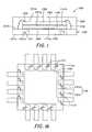
- FIG. 1is a cross-sectional view of a semiconductor package constructed in accordance with the present invention
- FIG. 1Ais a bottom plan view of the semiconductor package shown in FIG. 1 , excluding the encapsulating portion thereof;
- FIG. 1Bis a top plan view of the semiconductor package shown in FIG. 1 , excluding the encapsulating portion thereof;
- FIGS. 2A through 2Eare cross-sectional views illustrating a sequence of steps which may be employed for manufacturing the semiconductor package of the present invention.
- FIG. 1provides a cross-sectional view of a semiconductor package 100 constructed in accordance with the present invention.
- the semiconductor package 100comprises a plurality of identically configured leads 130 .
- Each of the leads 130defines a generally planar first (lower) surface 131 a and a generally planar second (upper) surface 131 b which is disposed in opposed relation to the first surface 131 a .
- Each lead 130further defines a generally planar third (lower) surface 131 c which is also disposed in opposed relation to the second surface 131 b and is laterally offset outwardly relative to the first surface 131 a .
- the thickness between the second and third surfaces 131 b , 131 cexceeds the thickness between the first and second surfaces 131 a , 131 b .
- the first surfaces 131 a of the leads 130are each preferably formed by a conventional half etching technique using chemical solutions.
- the semiconductor package 100includes a die paddle 135 which is of a predetermined thickness.
- the preferred thickness of the die paddle 135is preferably the same as the thickness between the second and third surfaces 131 b , 131 c of each of the leads 130 .
- the leads 130 and die paddle 135are oriented relative to each other such that the leads 130 are arranged about the periphery of the die paddle 135 in the manner best shown in FIG. 1 A.
- the die paddle 135has a generally square configuration, with the leads 130 being segregated into four sets of four, and each set extending along a respective one of the four peripheral edge segments defined by the die paddle 135 . As seen in FIGS.
- each lead 130is disposed in spaced relation to the corresponding peripheral edge segment of the die paddle 135 .
- Those of ordinary skill in the artwill recognize that differing numbers of leads 130 in differing arrangements may be included in the semiconductor package 100 , with the size, shape and arrangement of the leads 130 and die paddle 135 as shown in FIGS. 1 , 1 A and 1 B being for exemplary purposes only.
- the semiconductor package 100 of the present inventionfurther comprises a first semiconductor die 110 which defines a first surface 111 a and a second surface 111 b which is disposed in opposed relation to the first surface 111 a .
- the first semiconductor die 110further includes a plurality of bond pads 113 which are disposed on the first surface 111 a thereof.
- portions of the first surface 111 a of the first semiconductor die 110are bonded to the second surface 131 b of each lead 130 and to the top surface of the die paddle 135 through the use of a layer of a die attach material 160 .
- the die attach material 160may be any one of a non-conductive epoxy, a non-conductive polyimide, a non-conductive double-faced adhesive tape or its equivalent, with the present invention not being limited by any particular die attach material 160 .
- the semiconductor package 100includes a second semiconductor die 120 .
- the second semiconductor die 120defines a first surface 121 a and a second surface 121 b which is disposed in opposed relation to the first surface 121 a . Disposed on the second surface 121 b blare a plurality of bond pads 123 .
- the first surface 121 a of the second semiconductor die 120is bonded to the second surface 111 b of the first semiconductor die 110 by another layer of the die attach material 160 .
- the first semiconductor die 110 and leads 130are arranged relative to each other such that the bond pads 113 of the first semiconductor die 110 are each oriented between a respective pair of the leads 130 when the first surface 111 a of the first semiconductor die 110 is bonded to the second surfaces 131 b of the leads 130 .
- each bond pad 113 of the first semiconductor die 120is electrically connected to the first surface 131 a of a respective one of the leads 130 by a first conductive connector 151 such as a conductive wire.
- each bond pad 123 of the second semiconductor die 120is electrically connected to the second surface 131 b of a respective one of the leads 130 by a second conductive connector 153 such as a conductive wire.
- the conductive connectors 151 , 153may each be any one of a gold wire, an aluminum wire, or its equivalent, with the present invention not being limited by any particular material for the conductive connectors 151 , 153 .
- the bond pads 113 of the first semiconductor die 110are each located between a respective pair of leads 130 .
- the electrical connection between the bond pads 113 and the first surfaces 131 a of the leads 130 through the use of the conductive connectors 151can be accomplished in a manner wherein the conductive connectors 151 are each located inwardly relative to the peripheral edge of the first semiconductor die 110 .
- the peripheral edge of the first semiconductor die 110extends to approximately that portion of the second surface 131 b of each lead 130 which is disposed in opposed relation to the third surface 131 c.
- the first and second semiconductor dies 110 , 120 , the leads 130 , and the conductive connectors 151 , 153are each encapsulated by an encapsulant in order to protect the same from the external environment.
- the hardening of the encapsulantdefines an encapsulating portion 180 of the semiconductor package 100 .
- the encapsulating portion 180is formed such that the third surface 131 c of each of the leads 130 and the bottom surface of the die paddle 135 are exposed within the encapsulating portion 180 , and in particular the bottom surface defined thereby. Also exposed in the side surfaces of the encapsulating portion 180 is the outermost end of each of the leads 130 .
- the exposed third surfaces 131 c of the leads 130may be electrically connected to an external device (e.g., a motherboard). Additionally, the exposed third surfaces 131 c of the leads 130 and bottom surface of the die paddle 135 within the encapsulating portion 180 function as heat sinks which allow for the emission of heat generated by the first and second semiconductor dies 110 , 120 .
- first and second semiconductor dies 110 , 120will have identical functions since the semiconductor dies 110 , 120 are electrically connected to common leads 130 . However, it is also contemplated that the first and second semiconductor dies 110 , 120 may have different functions. In this case, the first semiconductor die 110 would be electrically connected to the first surfaces 131 a of certain ones of the leads 130 , with the second semiconductor die 120 being electrically connected to the second surfaces 131 b of certain ones of the leads 130 which are not electrically connected to the first semiconductor die 110 . As such, the first and second semiconductor dies 110 , 120 would not be electrically connected to any common lead 130 . The orientation of the conductive connectors 151 inwardly of the peripheral edges of the stacked semiconductor dies 110 , 120 allows for a reduction in the size of the semiconductor package 100 .
- the manufacturing method for the semiconductor package 100 of the present inventionpreferably comprises the initial step of providing the leads 130 and die paddle 135 oriented relative to each other in the above-described manner. Thereafter, the first surface 111 a of the first semiconductor die 110 is bonded to the second surface 131 b of each of the leads 130 and to the top surface of the die paddle 135 through the use of the die attach material 160 in the above-described manner (FIG. 2 A).
- the first semiconductor die 110 and the leads 130are oriented relative to each other such that the bond pads 113 of the first semiconductor die 110 are not in direct contact with any of the second surfaces 131 b of the leads 130 , but rather are each oriented between a respective pair of the leads 130 .
- the bond pads 113 of the first semiconductor die 110are electrically connected to respective ones of the first surfaces 131 a of the leads 130 through the use of the first conductive connectors 151 (FIG. 2 B). Thereafter, the first surface 121 a of the second semiconductor die 120 is bonded to the second surface 111 b of the first semiconductor die 110 by another layer of the die attach material 160 (FIG. 2 C).
- the bond pads 123 of the second semiconductor die 120are electrically connected to respective ones of the second surfaces 131 b of the leads 130 through the use of the second conductive connectors 153 in the above-described manner (FIG. 2 D).
- the encapsulantis applied to the first and second semiconductor dies 110 , 120 , the leads 130 and the first and second conductive connectors 151 , 153 to encapsulate the same and form the encapsulating portion 180 (FIG. 2 E).
- the encapsulating portion 180protects the first and second semiconductor dies 110 , 120 , the leads 130 , and the first and second conductive connectors 151 , 153 from the external environment.
- the second semiconductor die 120may be bonded to the first semiconductor die 110 via a layer of the die attach material 160 , with the first semiconductor die 110 thereafter being bonded to the leads 130 in the above-described manner. It is further contemplated that the bonding order of the first and second conductive connectors 151 , 153 used to facilitate the electrical connection of the first and second semiconductor dies 110 , 120 , respectively, to the leads 130 can be changed or reversed from that described above if warranted by the circumstance.
Landscapes
- Engineering & Computer Science (AREA)
- Computer Hardware Design (AREA)
- Microelectronics & Electronic Packaging (AREA)
- Power Engineering (AREA)
- Physics & Mathematics (AREA)
- Condensed Matter Physics & Semiconductors (AREA)
- General Physics & Mathematics (AREA)
- Geometry (AREA)
- Lead Frames For Integrated Circuits (AREA)
Abstract
Description
Claims (16)
Priority Applications (1)
| Application Number | Priority Date | Filing Date | Title |
|---|---|---|---|
| US11/079,836US20050156292A1 (en) | 2001-01-15 | 2005-03-14 | Reduced size semiconductor package with stacked dies |
Applications Claiming Priority (2)
| Application Number | Priority Date | Filing Date | Title |
|---|---|---|---|
| KR1020010002163AKR100731007B1 (en) | 2001-01-15 | 2001-01-15 | Stacked Semiconductor Packages |
| KR2001-02163 | 2001-01-15 |
Related Child Applications (1)
| Application Number | Title | Priority Date | Filing Date |
|---|---|---|---|
| US11/079,836ContinuationUS20050156292A1 (en) | 2001-01-15 | 2005-03-14 | Reduced size semiconductor package with stacked dies |
Publications (2)
| Publication Number | Publication Date |
|---|---|
| US20020093087A1 US20020093087A1 (en) | 2002-07-18 |
| US6927478B2true US6927478B2 (en) | 2005-08-09 |
Family
ID=19704636
Family Applications (2)
| Application Number | Title | Priority Date | Filing Date |
|---|---|---|---|
| US10/043,946Expired - LifetimeUS6927478B2 (en) | 2001-01-15 | 2002-01-11 | Reduced size semiconductor package with stacked dies |
| US11/079,836AbandonedUS20050156292A1 (en) | 2001-01-15 | 2005-03-14 | Reduced size semiconductor package with stacked dies |
Family Applications After (1)
| Application Number | Title | Priority Date | Filing Date |
|---|---|---|---|
| US11/079,836AbandonedUS20050156292A1 (en) | 2001-01-15 | 2005-03-14 | Reduced size semiconductor package with stacked dies |
Country Status (2)
| Country | Link |
|---|---|
| US (2) | US6927478B2 (en) |
| KR (1) | KR100731007B1 (en) |
Cited By (88)
| Publication number | Priority date | Publication date | Assignee | Title |
|---|---|---|---|---|
| US20040104457A1 (en)* | 2002-11-27 | 2004-06-03 | United Test And Assembly Test Center Ltd. | High density chip scale leadframe package and method of manufacturing the package |
| US20040262754A1 (en)* | 2002-02-01 | 2004-12-30 | Khan Reza-Ur Rahman | IC die support structures for ball grid array package fabrication |
| US20050156292A1 (en)* | 2001-01-15 | 2005-07-21 | Paek Jong S. | Reduced size semiconductor package with stacked dies |
| US20060192294A1 (en)* | 2004-11-15 | 2006-08-31 | Chippac, Inc | Chip scale package having flip chip interconnect on die paddle |
| US7560804B1 (en) | 1998-06-24 | 2009-07-14 | Amkor Technology, Inc. | Integrated circuit package and method of making the same |
| US7687899B1 (en) | 2007-08-07 | 2010-03-30 | Amkor Technology, Inc. | Dual laminate package structure with embedded elements |
| US20100123227A1 (en)* | 2008-11-17 | 2010-05-20 | Frederick Rodriguez Dahilig | Integrated circuit packaging system with increased connectivity and method of manufacture thereof |
| US7723852B1 (en) | 2008-01-21 | 2010-05-25 | Amkor Technology, Inc. | Stacked semiconductor package and method of making same |
| US7732899B1 (en) | 2005-12-02 | 2010-06-08 | Amkor Technology, Inc. | Etch singulated semiconductor package |
| US7768135B1 (en) | 2008-04-17 | 2010-08-03 | Amkor Technology, Inc. | Semiconductor package with fast power-up cycle and method of making same |
| US7777351B1 (en) | 2007-10-01 | 2010-08-17 | Amkor Technology, Inc. | Thin stacked interposer package |
| US7808084B1 (en) | 2008-05-06 | 2010-10-05 | Amkor Technology, Inc. | Semiconductor package with half-etched locking features |
| US7847392B1 (en) | 2008-09-30 | 2010-12-07 | Amkor Technology, Inc. | Semiconductor device including leadframe with increased I/O |
| US7847386B1 (en) | 2007-11-05 | 2010-12-07 | Amkor Technology, Inc. | Reduced size stacked semiconductor package and method of making the same |
| US7875963B1 (en) | 2008-11-21 | 2011-01-25 | Amkor Technology, Inc. | Semiconductor device including leadframe having power bars and increased I/O |
| US7928542B2 (en) | 2001-03-27 | 2011-04-19 | Amkor Technology, Inc. | Lead frame for semiconductor package |
| US7956453B1 (en) | 2008-01-16 | 2011-06-07 | Amkor Technology, Inc. | Semiconductor package with patterning layer and method of making same |
| US7960818B1 (en) | 2009-03-04 | 2011-06-14 | Amkor Technology, Inc. | Conformal shield on punch QFN semiconductor package |
| US7977774B2 (en) | 2007-07-10 | 2011-07-12 | Amkor Technology, Inc. | Fusion quad flat semiconductor package |
| US7982298B1 (en) | 2008-12-03 | 2011-07-19 | Amkor Technology, Inc. | Package in package semiconductor device |
| US7989933B1 (en) | 2008-10-06 | 2011-08-02 | Amkor Technology, Inc. | Increased I/O leadframe and semiconductor device including same |
| US20110193213A1 (en)* | 2010-02-05 | 2011-08-11 | Hynix Semiconductor Inc. | Stacked semiconductor package |
| US8008758B1 (en) | 2008-10-27 | 2011-08-30 | Amkor Technology, Inc. | Semiconductor device with increased I/O leadframe |
| US8026589B1 (en) | 2009-02-23 | 2011-09-27 | Amkor Technology, Inc. | Reduced profile stackable semiconductor package |
| US8058715B1 (en) | 2009-01-09 | 2011-11-15 | Amkor Technology, Inc. | Package in package device for RF transceiver module |
| US8067821B1 (en) | 2008-04-10 | 2011-11-29 | Amkor Technology, Inc. | Flat semiconductor package with half package molding |
| US8072050B1 (en) | 2008-11-18 | 2011-12-06 | Amkor Technology, Inc. | Semiconductor device with increased I/O leadframe including passive device |
| US8080000B2 (en) | 2004-04-21 | 2011-12-20 | Acclarent, Inc. | Methods and apparatus for treating disorders of the ear nose and throat |
| US8089145B1 (en) | 2008-11-17 | 2012-01-03 | Amkor Technology, Inc. | Semiconductor device including increased capacity leadframe |
| US8089159B1 (en) | 2007-10-03 | 2012-01-03 | Amkor Technology, Inc. | Semiconductor package with increased I/O density and method of making the same |
| US8088101B2 (en) | 2004-04-21 | 2012-01-03 | Acclarent, Inc. | Devices, systems and methods for treating disorders of the ear, nose and throat |
| US8100933B2 (en) | 2002-09-30 | 2012-01-24 | Acclarent, Inc. | Method for treating obstructed paranasal frontal sinuses |
| US8114062B2 (en) | 2004-04-21 | 2012-02-14 | Acclarent, Inc. | Devices and methods for delivering therapeutic substances for the treatment of sinusitis and other disorders |
| US8114113B2 (en) | 2005-09-23 | 2012-02-14 | Acclarent, Inc. | Multi-conduit balloon catheter |
| US8118757B2 (en) | 2007-04-30 | 2012-02-21 | Acclarent, Inc. | Methods and devices for ostium measurement |
| US8125064B1 (en) | 2008-07-28 | 2012-02-28 | Amkor Technology, Inc. | Increased I/O semiconductor package and method of making same |
| US8142422B2 (en) | 2004-04-21 | 2012-03-27 | Acclarent, Inc. | Devices, systems and methods for diagnosing and treating sinusitis and other disorders of the ears, nose and/or throat |
| US8146400B2 (en) | 2004-04-21 | 2012-04-03 | Acclarent, Inc. | Endoscopic methods and devices for transnasal procedures |
| US8172828B2 (en) | 2004-04-21 | 2012-05-08 | Acclarent, Inc. | Apparatus and methods for dilating and modifying ostia of paranasal sinuses and other intranasal or paranasal structures |
| US8182432B2 (en) | 2008-03-10 | 2012-05-22 | Acclarent, Inc. | Corewire design and construction for medical devices |
| US8184453B1 (en) | 2008-07-31 | 2012-05-22 | Amkor Technology, Inc. | Increased capacity semiconductor package |
| US8190389B2 (en) | 2006-05-17 | 2012-05-29 | Acclarent, Inc. | Adapter for attaching electromagnetic image guidance components to a medical device |
| US8318287B1 (en) | 1998-06-24 | 2012-11-27 | Amkor Technology, Inc. | Integrated circuit package and method of making the same |
| US8388642B2 (en) | 2005-01-18 | 2013-03-05 | Acclarent, Inc. | Implantable devices and methods for treating sinusitis and other disorders |
| US8414473B2 (en) | 2004-04-21 | 2013-04-09 | Acclarent, Inc. | Methods and apparatus for treating disorders of the ear nose and throat |
| US8435290B2 (en) | 2009-03-31 | 2013-05-07 | Acclarent, Inc. | System and method for treatment of non-ventilating middle ear by providing a gas pathway through the nasopharynx |
| US8441110B1 (en) | 2006-06-21 | 2013-05-14 | Amkor Technology, Inc. | Side leaded, bottom exposed pad and bottom exposed lead fusion quad flat semiconductor package |
| US8439687B1 (en) | 2006-12-29 | 2013-05-14 | Acclarent, Inc. | Apparatus and method for simulated insertion and positioning of guidewares and other interventional devices |
| US8487420B1 (en) | 2008-12-08 | 2013-07-16 | Amkor Technology, Inc. | Package in package semiconductor device with film over wire |
| US8485199B2 (en) | 2007-05-08 | 2013-07-16 | Acclarent, Inc. | Methods and devices for protecting nasal turbinate during surgery |
| US8575742B1 (en) | 2009-04-06 | 2013-11-05 | Amkor Technology, Inc. | Semiconductor device with increased I/O leadframe including power bars |
| US8648450B1 (en) | 2011-01-27 | 2014-02-11 | Amkor Technology, Inc. | Semiconductor device including leadframe with a combination of leads and lands |
| US8674485B1 (en) | 2010-12-08 | 2014-03-18 | Amkor Technology, Inc. | Semiconductor device including leadframe with downsets |
| US8680656B1 (en) | 2009-01-05 | 2014-03-25 | Amkor Technology, Inc. | Leadframe structure for concentrated photovoltaic receiver package |
| US8702626B1 (en) | 2004-04-21 | 2014-04-22 | Acclarent, Inc. | Guidewires for performing image guided procedures |
| US8715169B2 (en) | 2004-04-21 | 2014-05-06 | Acclarent, Inc. | Devices, systems and methods useable for treating sinusitis |
| US8740929B2 (en) | 2001-02-06 | 2014-06-03 | Acclarent, Inc. | Spacing device for releasing active substances in the paranasal sinus |
| US8747389B2 (en) | 2004-04-21 | 2014-06-10 | Acclarent, Inc. | Systems for treating disorders of the ear, nose and throat |
| US8764729B2 (en) | 2004-04-21 | 2014-07-01 | Acclarent, Inc. | Frontal sinus spacer |
| US8864787B2 (en) | 2004-04-21 | 2014-10-21 | Acclarent, Inc. | Ethmoidotomy system and implantable spacer devices having therapeutic substance delivery capability for treatment of paranasal sinusitis |
| US8894614B2 (en) | 2004-04-21 | 2014-11-25 | Acclarent, Inc. | Devices, systems and methods useable for treating frontal sinusitis |
| US8932276B1 (en) | 2004-04-21 | 2015-01-13 | Acclarent, Inc. | Shapeable guide catheters and related methods |
| US8951225B2 (en) | 2005-06-10 | 2015-02-10 | Acclarent, Inc. | Catheters with non-removable guide members useable for treatment of sinusitis |
| US8979888B2 (en) | 2008-07-30 | 2015-03-17 | Acclarent, Inc. | Paranasal ostium finder devices and methods |
| US9039657B2 (en) | 2004-08-04 | 2015-05-26 | Acclarent, Inc. | Implantable devices and methods for delivering drugs and other substances to treat sinusitis and other disorders |
| US9072626B2 (en) | 2009-03-31 | 2015-07-07 | Acclarent, Inc. | System and method for treatment of non-ventilating middle ear by providing a gas pathway through the nasopharynx |
| US9089258B2 (en) | 2004-04-21 | 2015-07-28 | Acclarent, Inc. | Endoscopic methods and devices for transnasal procedures |
| US9101384B2 (en) | 2004-04-21 | 2015-08-11 | Acclarent, Inc. | Devices, systems and methods for diagnosing and treating sinusitis and other disorders of the ears, Nose and/or throat |
| US9107574B2 (en) | 2004-04-21 | 2015-08-18 | Acclarent, Inc. | Endoscopic methods and devices for transnasal procedures |
| US9155492B2 (en) | 2010-09-24 | 2015-10-13 | Acclarent, Inc. | Sinus illumination lightwire device |
| US9184118B2 (en) | 2013-05-02 | 2015-11-10 | Amkor Technology Inc. | Micro lead frame structure having reinforcing portions and method |
| US9184148B2 (en) | 2013-10-24 | 2015-11-10 | Amkor Technology, Inc. | Semiconductor package and method therefor |
| US9265407B2 (en) | 2004-04-21 | 2016-02-23 | Acclarent, Inc. | Endoscopic methods and devices for transnasal procedures |
| US9351750B2 (en) | 2004-04-21 | 2016-05-31 | Acclarent, Inc. | Devices and methods for treating maxillary sinus disease |
| US9399121B2 (en) | 2004-04-21 | 2016-07-26 | Acclarent, Inc. | Systems and methods for transnasal dilation of passageways in the ear, nose or throat |
| US9433437B2 (en) | 2013-03-15 | 2016-09-06 | Acclarent, Inc. | Apparatus and method for treatment of ethmoid sinusitis |
| US9468362B2 (en) | 2004-04-21 | 2016-10-18 | Acclarent, Inc. | Endoscopic methods and devices for transnasal procedures |
| US9629684B2 (en) | 2013-03-15 | 2017-04-25 | Acclarent, Inc. | Apparatus and method for treatment of ethmoid sinusitis |
| US9631481B1 (en) | 2011-01-27 | 2017-04-25 | Amkor Technology, Inc. | Semiconductor device including leadframe with a combination of leads and lands and method |
| US9673122B2 (en) | 2014-05-02 | 2017-06-06 | Amkor Technology, Inc. | Micro lead frame structure having reinforcing portions and method |
| US9704725B1 (en) | 2012-03-06 | 2017-07-11 | Amkor Technology, Inc. | Semiconductor device with leadframe configured to facilitate reduced burr formation |
| US9820688B2 (en) | 2006-09-15 | 2017-11-21 | Acclarent, Inc. | Sinus illumination lightwire device |
| US10188413B1 (en) | 2004-04-21 | 2019-01-29 | Acclarent, Inc. | Deflectable guide catheters and related methods |
| US10206821B2 (en) | 2007-12-20 | 2019-02-19 | Acclarent, Inc. | Eustachian tube dilation balloon with ventilation path |
| US10524814B2 (en) | 2009-03-20 | 2020-01-07 | Acclarent, Inc. | Guide system with suction |
| US10811341B2 (en) | 2009-01-05 | 2020-10-20 | Amkor Technology Singapore Holding Pte Ltd. | Semiconductor device with through-mold via |
| US11065061B2 (en) | 2004-04-21 | 2021-07-20 | Acclarent, Inc. | Systems and methods for performing image guided procedures within the ear, nose, throat and paranasal sinuses |
| US11529502B2 (en) | 2004-04-21 | 2022-12-20 | Acclarent, Inc. | Apparatus and methods for dilating and modifying ostia of paranasal sinuses and other intranasal or paranasal structures |
Families Citing this family (8)
| Publication number | Priority date | Publication date | Assignee | Title |
|---|---|---|---|---|
| KR20050095586A (en)* | 2002-12-20 | 2005-09-29 | 코닌클리즈케 필립스 일렉트로닉스 엔.브이. | Electronic device and method of manufacturing same |
| US20050275089A1 (en)* | 2004-06-09 | 2005-12-15 | Joshi Rajeev D | Package and method for packaging an integrated circuit die |
| US7298026B2 (en)* | 2005-05-09 | 2007-11-20 | Stats Chippac Ltd. | Large die package and method for the fabrication thereof |
| US20070187836A1 (en)* | 2006-02-15 | 2007-08-16 | Texas Instruments Incorporated | Package on package design a combination of laminate and tape substrate, with back-to-back die combination |
| US20080217759A1 (en)* | 2007-03-06 | 2008-09-11 | Taiwan Solutions Systems Corp. | Chip package substrate and structure thereof |
| US8105880B2 (en)* | 2007-12-05 | 2012-01-31 | Analog Devices, Inc. | Method for attaching a semiconductor die to a leadframe, and a semiconductor device |
| US9711424B2 (en)* | 2012-09-17 | 2017-07-18 | Littelfuse, Inc. | Low thermal stress package for large area semiconductor dies |
| JP7346372B2 (en)* | 2020-09-08 | 2023-09-19 | 株式会社東芝 | semiconductor equipment |
Citations (103)
| Publication number | Priority date | Publication date | Assignee | Title |
|---|---|---|---|---|
| US3838984A (en) | 1973-04-16 | 1974-10-01 | Sperry Rand Corp | Flexible carrier and interconnect for uncased ic chips |
| US4054238A (en) | 1976-03-23 | 1977-10-18 | Western Electric Company, Inc. | Method, apparatus and lead frame for assembling leads with terminals on a substrate |
| JPS5745959A (en) | 1980-09-02 | 1982-03-16 | Nec Corp | Resin-sealed semiconductor device |
| JPS59227143A (en) | 1983-06-07 | 1984-12-20 | Dainippon Printing Co Ltd | Package of integrated circuit |
| US4530152A (en) | 1982-04-01 | 1985-07-23 | Compagnie Industrielle Des Telecommunications Cit-Alcatel | Method for encapsulating semiconductor components using temporary substrates |
| JPS60195957A (en) | 1984-03-19 | 1985-10-04 | Hitachi Ltd | lead frame |
| JPS6139555A (en) | 1984-07-31 | 1986-02-25 | Toshiba Corp | Resin sealed type semiconductor device with heat sink |
| JPS61248541A (en) | 1985-04-26 | 1986-11-05 | Matsushita Electronics Corp | Semiconductor device |
| JPS629639A (en) | 1985-07-05 | 1987-01-17 | Nec Yamagata Ltd | Manufacture of semiconductor device |
| US4707724A (en) | 1984-06-04 | 1987-11-17 | Hitachi, Ltd. | Semiconductor device and method of manufacturing thereof |
| US4756080A (en) | 1986-01-27 | 1988-07-12 | American Microsystems, Inc. | Metal foil semiconductor interconnection method |
| JPS63205935A (en) | 1987-02-23 | 1988-08-25 | Toshiba Corp | Resin-encapsulated semiconductor device with heat sink |
| JPS63233555A (en) | 1987-03-23 | 1988-09-29 | Toshiba Corp | Resin-encapsulated semiconductor device |
| US4812896A (en) | 1986-11-13 | 1989-03-14 | Olin Corporation | Metal electronic package sealed with thermoplastic having a grafted metal deactivator and antioxidant |
| JPH01106456A (en) | 1987-10-19 | 1989-04-24 | Matsushita Electric Ind Co Ltd | Semiconductor integrated circuit device |
| US5041902A (en) | 1989-12-14 | 1991-08-20 | Motorola, Inc. | Molded electronic package with compression structures |
| US5157480A (en) | 1991-02-06 | 1992-10-20 | Motorola, Inc. | Semiconductor device having dual electrical contact sites |
| US5172214A (en) | 1991-02-06 | 1992-12-15 | Motorola, Inc. | Leadless semiconductor device and method for making the same |
| US5172213A (en) | 1991-05-23 | 1992-12-15 | At&T Bell Laboratories | Molded circuit package having heat dissipating post |
| US5200362A (en) | 1989-09-06 | 1993-04-06 | Motorola, Inc. | Method of attaching conductive traces to an encapsulated semiconductor die using a removable transfer film |
| US5200809A (en) | 1991-09-27 | 1993-04-06 | Vlsi Technology, Inc. | Exposed die-attach heatsink package |
| US5214845A (en) | 1992-05-11 | 1993-06-01 | Micron Technology, Inc. | Method for producing high speed integrated circuits |
| US5216278A (en) | 1990-12-04 | 1993-06-01 | Motorola, Inc. | Semiconductor device having a pad array carrier package |
| US5221642A (en) | 1991-08-15 | 1993-06-22 | Staktek Corporation | Lead-on-chip integrated circuit fabrication method |
| US5258094A (en) | 1991-09-18 | 1993-11-02 | Nec Corporation | Method for producing multilayer printed wiring boards |
| US5277972A (en) | 1988-09-29 | 1994-01-11 | Tomoegawa Paper Co., Ltd. | Adhesive tapes |
| US5278446A (en) | 1992-07-06 | 1994-01-11 | Motorola, Inc. | Reduced stress plastic package |
| US5279029A (en) | 1990-08-01 | 1994-01-18 | Staktek Corporation | Ultra high density integrated circuit packages method |
| KR940001979A (en) | 1992-07-28 | 1994-02-16 | 존 해밀톤 무어 | Lining of molten metal processing container |
| JPH0692076A (en) | 1992-09-16 | 1994-04-05 | Oki Electric Ind Co Ltd | Lead frame form for ic card module |
| US5332864A (en) | 1991-12-27 | 1994-07-26 | Vlsi Technology, Inc. | Integrated circuit package having an interposer |
| US5336931A (en) | 1993-09-03 | 1994-08-09 | Motorola, Inc. | Anchoring method for flow formed integrated circuit covers |
| US5343076A (en) | 1990-07-21 | 1994-08-30 | Mitsui Petrochemical Industries, Ltd. | Semiconductor device with an airtight space formed internally within a hollow package |
| US5406124A (en) | 1992-12-04 | 1995-04-11 | Mitsui Toatsu Chemicals, Inc. | Insulating adhesive tape, and lead frame and semiconductor device employing the tape |
| US5424576A (en) | 1993-03-22 | 1995-06-13 | Motorola, Inc. | Semiconductor device having x-shaped die support member and method for making the same |
| KR950018924A (en) | 1993-12-09 | 1995-07-22 | 박홍기 | Manufacturing method of suede artificial leather |
| US5435057A (en) | 1990-10-30 | 1995-07-25 | International Business Machines Corporation | Interconnection method and structure for organic circuit boards |
| JPH07312405A (en) | 1994-05-17 | 1995-11-28 | Hitachi Ltd | Semiconductor device |
| US5474958A (en) | 1993-05-04 | 1995-12-12 | Motorola, Inc. | Method for making semiconductor device having no die supporting surface |
| JPH08125066A (en) | 1994-10-26 | 1996-05-17 | Dainippon Printing Co Ltd | Resin-sealed semiconductor device, lead frame used therefor, and method of manufacturing resin-sealed semiconductor device |
| US5521429A (en) | 1993-11-25 | 1996-05-28 | Sanyo Electric Co., Ltd. | Surface-mount flat package semiconductor device |
| US5534467A (en)* | 1993-03-18 | 1996-07-09 | Lsi Logic Corporation | Semiconductor packages for high I/O semiconductor dies |
| JPH08306853A (en) | 1995-05-09 | 1996-11-22 | Fujitsu Ltd | Semiconductor device, method of manufacturing the same, and method of manufacturing lead frame |
| JPH098206A (en) | 1995-06-19 | 1997-01-10 | Dainippon Printing Co Ltd | Lead frame and bga resin sealed semiconductor device |
| JPH098205A (en) | 1995-06-14 | 1997-01-10 | Dainippon Printing Co Ltd | Resin-sealed semiconductor device |
| JPH098207A (en) | 1995-06-21 | 1997-01-10 | Dainippon Printing Co Ltd | Resin-sealed semiconductor device |
| US5604376A (en) | 1994-06-30 | 1997-02-18 | Digital Equipment Corporation | Paddleless molded plastic semiconductor chip package |
| US5608267A (en) | 1992-09-17 | 1997-03-04 | Olin Corporation | Molded plastic semiconductor package including heat spreader |
| JPH0992775A (en) | 1995-09-22 | 1997-04-04 | Hitachi Cable Ltd | Semiconductor device |
| US5639990A (en) | 1992-06-05 | 1997-06-17 | Mitsui Toatsu Chemicals, Inc. | Solid printed substrate and electronic circuit package using the same |
| US5640047A (en) | 1995-09-25 | 1997-06-17 | Mitsui High-Tec, Inc. | Ball grid assembly type semiconductor device having a heat diffusion function and an electric and magnetic shielding function |
| US5641997A (en) | 1993-09-14 | 1997-06-24 | Kabushiki Kaisha Toshiba | Plastic-encapsulated semiconductor device |
| US5646831A (en) | 1995-12-28 | 1997-07-08 | Vlsi Technology, Inc. | Electrically enhanced power quad flat pack arrangement |
| US5650663A (en) | 1995-07-03 | 1997-07-22 | Olin Corporation | Electronic package with improved thermal properties |
| EP0794572A2 (en) | 1996-03-07 | 1997-09-10 | Matsushita Electronics Corporation | Electronic component, method for making the same, and lead frame and mold assembly for use therein |
| US5683806A (en) | 1988-09-29 | 1997-11-04 | Tomoegawa Paper Co., Ltd. | Adhesive tapes |
| KR970072358A (en) | 1996-04-01 | 1997-11-07 | 황인길 | Method and structure for manufacturing semiconductor package |
| US5689135A (en)* | 1995-12-19 | 1997-11-18 | Micron Technology, Inc. | Multi-chip device and method of fabrication employing leads over and under processes |
| US5696666A (en) | 1995-10-11 | 1997-12-09 | Motorola, Inc. | Low profile exposed die chip carrier package |
| US5701034A (en) | 1994-05-03 | 1997-12-23 | Amkor Electronics, Inc. | Packaged semiconductor die including heat sink with locking feature |
| US5710064A (en) | 1994-08-16 | 1998-01-20 | Samsung Electronics Co., Ltd. | Method for manufacturing a semiconductor package |
| US5736432A (en) | 1996-09-20 | 1998-04-07 | National Semiconductor Corporation | Lead frame with lead finger locking feature and method for making same |
| US5776798A (en) | 1996-09-04 | 1998-07-07 | Motorola, Inc. | Semiconductor package and method thereof |
| DE19734794A1 (en) | 1997-01-09 | 1998-07-16 | Mitsubishi Electric Corp | Wiring part and lead frame with the wiring part |
| US5783861A (en) | 1994-03-29 | 1998-07-21 | Lg Semicon Co., Ltd. | Semiconductor package and lead frame |
| US5814883A (en)* | 1995-10-04 | 1998-09-29 | Mitsubishi Denki Kabushiki Kaisha | Packaged semiconductor chip |
| US5814881A (en)* | 1996-12-20 | 1998-09-29 | Lsi Logic Corporation | Stacked integrated chip package and method of making same |
| US5821615A (en)* | 1995-12-06 | 1998-10-13 | Lg Semicon Co., Ltd. | Semiconductor chip package having clip-type outlead and fabrication method of same |
| US5835988A (en) | 1996-03-27 | 1998-11-10 | Mitsubishi Denki Kabushiki Kaisha | Packed semiconductor device with wrap around external leads |
| US5859471A (en) | 1992-11-17 | 1999-01-12 | Shinko Electric Industries Co., Ltd. | Semiconductor device having tab tape lead frame with reinforced outer leads |
| US5866939A (en) | 1996-01-21 | 1999-02-02 | Anam Semiconductor Inc. | Lead end grid array semiconductor package |
| US5877043A (en) | 1996-02-01 | 1999-03-02 | International Business Machines Corporation | Electronic package with strain relief means and method of making |
| US5894108A (en) | 1997-02-11 | 1999-04-13 | National Semiconductor Corporation | Plastic package with exposed die |
| US5903049A (en)* | 1997-10-29 | 1999-05-11 | Mitsubishi Denki Kabushiki Kaisha | Semiconductor module comprising semiconductor packages |
| US5977630A (en) | 1997-08-15 | 1999-11-02 | International Rectifier Corp. | Plural semiconductor die housed in common package with split heat sink |
| US5981314A (en) | 1996-10-31 | 1999-11-09 | Amkor Technology, Inc. | Near chip size integrated circuit package |
| US5986885A (en) | 1997-04-08 | 1999-11-16 | Integrated Device Technology, Inc. | Semiconductor package with internal heatsink and assembly method |
| US6001671A (en) | 1996-04-18 | 1999-12-14 | Tessera, Inc. | Methods for manufacturing a semiconductor package having a sacrificial layer |
| US6025640A (en) | 1997-07-16 | 2000-02-15 | Dai Nippon Insatsu Kabushiki Kaisha | Resin-sealed semiconductor device, circuit member for use therein and method of manufacturing resin-sealed semiconductor device |
| US6031279A (en)* | 1996-09-02 | 2000-02-29 | Siemens Aktiengesellschaft | Power semiconductor component |
| USRE36613E (en)* | 1993-04-06 | 2000-03-14 | Micron Technology, Inc. | Multi-chip stacked devices |
| US6072228A (en) | 1996-10-25 | 2000-06-06 | Micron Technology, Inc. | Multi-part lead frame with dissimilar materials and method of manufacturing |
| US6087715A (en)* | 1997-04-22 | 2000-07-11 | Kabushiki Kaisha Toshiba | Semiconductor device, and manufacturing method of the same |
| US6087722A (en)* | 1998-05-28 | 2000-07-11 | Samsung Electronics Co., Ltd. | Multi-chip package |
| US6100594A (en)* | 1998-01-14 | 2000-08-08 | Sharp Kabushiki Kaisha | Semiconductor device and method of manufacturing the same |
| US6118184A (en)* | 1997-07-18 | 2000-09-12 | Sharp Kabushiki Kaisha | Semiconductor device sealed with a sealing resin and including structure to balance sealing resin flow |
| US6130473A (en) | 1998-04-02 | 2000-10-10 | National Semiconductor Corporation | Lead frame chip scale package |
| US6130115A (en) | 1996-10-22 | 2000-10-10 | Matsushita Electronics Corporation | Plastic encapsulated semiconductor device and method of manufacturing the same |
| US6143981A (en) | 1998-06-24 | 2000-11-07 | Amkor Technology, Inc. | Plastic integrated circuit package and method and leadframe for making the package |
| US6181002B1 (en)* | 1998-12-22 | 2001-01-30 | Sharp Kabushiki Kaisha | Semiconductor device having a plurality of semiconductor chips |
| US6198171B1 (en)* | 1999-12-30 | 2001-03-06 | Siliconware Precision Industries Co., Ltd. | Thermally enhanced quad flat non-lead package of semiconductor |
| US6225146B1 (en) | 1996-12-24 | 2001-05-01 | Matsushita Electronics Corporation | Lead frame, method of manufacturing lead frame, semiconductor device and method of manufacturing semiconductor device |
| US6229200B1 (en) | 1998-06-10 | 2001-05-08 | Asat Limited | Saw-singulated leadless plastic chip carrier |
| US6281568B1 (en) | 1998-10-21 | 2001-08-28 | Amkor Technology, Inc. | Plastic integrated circuit device package and leadframe having partially undercut leads and die pad |
| US6294100B1 (en) | 1998-06-10 | 2001-09-25 | Asat Ltd | Exposed die leadless plastic chip carrier |
| US6303984B1 (en)* | 1997-08-12 | 2001-10-16 | Micron Technology, Inc. | Lead frame including angle iron tie bar |
| US6316838B1 (en)* | 1999-10-29 | 2001-11-13 | Fujitsu Limited | Semiconductor device |
| US20020011654A1 (en)* | 2000-07-25 | 2002-01-31 | Naoto Kimura | Semiconductor device |
| US6384472B1 (en)* | 2000-03-24 | 2002-05-07 | Siliconware Precision Industries Co., Ltd | Leadless image sensor package structure and method for making the same |
| US6410979B2 (en)* | 1998-12-21 | 2002-06-25 | Nec Corporation | Ball-grid-array semiconductor device with protruding terminals |
| KR20020049944A (en)* | 2000-12-20 | 2002-06-26 | 박종섭 | semiconductor package and method for fabricating the same |
| US6452279B2 (en)* | 2000-07-14 | 2002-09-17 | Mitsubishi Denki Kabushiki Kaisha | Semiconductor device |
| US6559525B2 (en)* | 2000-01-13 | 2003-05-06 | Siliconware Precision Industries Co., Ltd. | Semiconductor package having heat sink at the outer surface |
Family Cites Families (72)
| Publication number | Priority date | Publication date | Assignee | Title |
|---|---|---|---|---|
| US2596993A (en)* | 1949-01-13 | 1952-05-20 | United Shoe Machinery Corp | Method and mold for covering of eyelets by plastic injection |
| US3435815A (en)* | 1966-07-15 | 1969-04-01 | Micro Tech Mfg Inc | Wafer dicer |
| US3734660A (en)* | 1970-01-09 | 1973-05-22 | Tuthill Pump Co | Apparatus for fabricating a bearing device |
| US4189342A (en)* | 1971-10-07 | 1980-02-19 | U.S. Philips Corporation | Semiconductor device comprising projecting contact layers |
| JPS5479563A (en)* | 1977-12-07 | 1979-06-25 | Kyushu Nippon Electric | Lead frame for semiconductor |
| US4332537A (en)* | 1978-07-17 | 1982-06-01 | Dusan Slepcevic | Encapsulation mold with removable cavity plates |
| JPS5521128A (en)* | 1978-08-02 | 1980-02-15 | Hitachi Ltd | Lead frame used for semiconductor device and its assembling |
| JPS5588356A (en)* | 1978-12-27 | 1980-07-04 | Hitachi Ltd | Semiconductor device |
| US4289922A (en)* | 1979-09-04 | 1981-09-15 | Plessey Incorporated | Integrated circuit package and lead frame |
| US4417266A (en)* | 1981-08-14 | 1983-11-22 | Amp Incorporated | Power and ground plane structure for chip carrier |
| US4451224A (en)* | 1982-03-25 | 1984-05-29 | General Electric Company | Mold device for making plastic articles from resin |
| US4646710A (en)* | 1982-09-22 | 1987-03-03 | Crystal Systems, Inc. | Multi-wafer slicing with a fixed abrasive |
| US4737839A (en)* | 1984-03-19 | 1988-04-12 | Trilogy Computer Development Partners, Ltd. | Semiconductor chip mounting system |
| US4862246A (en)* | 1984-09-26 | 1989-08-29 | Hitachi, Ltd. | Semiconductor device lead frame with etched through holes |
| US4862245A (en)* | 1985-04-18 | 1989-08-29 | International Business Machines Corporation | Package semiconductor chip |
| US4727633A (en)* | 1985-08-08 | 1988-03-01 | Tektronix, Inc. | Method of securing metallic members together |
| US5087961A (en)* | 1987-01-28 | 1992-02-11 | Lsi Logic Corporation | Semiconductor device package |
| KR960006710B1 (en)* | 1987-02-25 | 1996-05-22 | 가부시기가이샤 히다찌세이사꾸쇼 | Surface mount plastic package semiconductor integrated circuit and the manufacturing method thereof and well asmount struct |
| US5059379A (en)* | 1987-07-20 | 1991-10-22 | Mitsubishi Denki Kabushiki Kaisha | Method of resin sealing semiconductor devices |
| US4942454A (en)* | 1987-08-05 | 1990-07-17 | Mitsubishi Denki Kabushiki Kaisha | Resin sealed semiconductor device |
| AU2309388A (en)* | 1987-08-26 | 1989-03-31 | Matsushita Electric Industrial Co., Ltd. | Integrated circuit device and method of producing the same |
| US4987475A (en)* | 1988-02-29 | 1991-01-22 | Digital Equipment Corporation | Alignment of leads for ceramic integrated circuit packages |
| US4907067A (en)* | 1988-05-11 | 1990-03-06 | Texas Instruments Incorporated | Thermally efficient power device package |
| US5096852A (en)* | 1988-06-02 | 1992-03-17 | Burr-Brown Corporation | Method of making plastic encapsulated multichip hybrid integrated circuits |
| US5157475A (en)* | 1988-07-08 | 1992-10-20 | Oki Electric Industry Co., Ltd. | Semiconductor device having a particular conductive lead structure |
| US4935803A (en)* | 1988-09-09 | 1990-06-19 | Motorola, Inc. | Self-centering electrode for power devices |
| US5057900A (en)* | 1988-10-17 | 1991-10-15 | Semiconductor Energy Laboratory Co., Ltd. | Electronic device and a manufacturing method for the same |
| US5018003A (en)* | 1988-10-20 | 1991-05-21 | Mitsubishi Denki Kabushiki Kaisha | Lead frame and semiconductor device |
| US5266834A (en)* | 1989-03-13 | 1993-11-30 | Hitachi Ltd. | Semiconductor device and an electronic device with the semiconductor devices mounted thereon |
| US5070039A (en)* | 1989-04-13 | 1991-12-03 | Texas Instruments Incorporated | Method of making an integrated circuit using a pre-served dam bar to reduce mold flash and to facilitate flash removal |
| JPH02306639A (en)* | 1989-05-22 | 1990-12-20 | Toshiba Corp | Resin encapsulating method for semiconductor device |
| US5417905A (en)* | 1989-05-26 | 1995-05-23 | Esec (Far East) Limited | Method of making a card having decorations on both faces |
| FR2659157B2 (en)* | 1989-05-26 | 1994-09-30 | Lemaire Gerard | METHOD FOR MANUFACTURING A CARD, SAID CARD, AND CARD OBTAINED BY THIS PROCESS. |
| EP0405755B1 (en)* | 1989-05-31 | 1995-11-29 | Fujitsu Limited | Pin grid array packaging structure |
| US5175060A (en)* | 1989-07-01 | 1992-12-29 | Ibiden Co., Ltd. | Leadframe semiconductor-mounting substrate having a roughened adhesive conductor circuit substrate and method of producing the same |
| JPH0671062B2 (en)* | 1989-08-30 | 1994-09-07 | 株式会社東芝 | Resin-sealed semiconductor device |
| US5118298A (en)* | 1991-04-04 | 1992-06-02 | Advanced Interconnections Corporation | Through hole mounting of integrated circuit adapter leads |
| US5151039A (en)* | 1990-04-06 | 1992-09-29 | Advanced Interconnections Corporation | Integrated circuit adapter having gullwing-shaped leads |
| US5029386A (en)* | 1990-09-17 | 1991-07-09 | Hewlett-Packard Company | Hierarchical tape automated bonding method |
| US5335771A (en)* | 1990-09-25 | 1994-08-09 | R. H. Murphy Company, Inc. | Spacer trays for stacking storage trays with integrated circuits |
| US5391439A (en)* | 1990-09-27 | 1995-02-21 | Dai Nippon Printing Co., Ltd. | Leadframe adapted to support semiconductor elements |
| US5281849A (en)* | 1991-05-07 | 1994-01-25 | Singh Deo Narendra N | Semiconductor package with segmented lead frame |
| US5168368A (en)* | 1991-05-09 | 1992-12-01 | International Business Machines Corporation | Lead frame-chip package with improved configuration |
| JP2518569B2 (en)* | 1991-09-19 | 1996-07-24 | 三菱電機株式会社 | Semiconductor device |
| JPH06120374A (en)* | 1992-03-31 | 1994-04-28 | Amkor Electron Inc | Semiconductor package structure, semicon- ductor packaging method and heat sink for semiconductor package |
| US5250841A (en)* | 1992-04-06 | 1993-10-05 | Motorola, Inc. | Semiconductor device with test-only leads |
| JPH05291345A (en)* | 1992-04-07 | 1993-11-05 | Mitsubishi Electric Corp | Semiconductor device |
| JPH0637202A (en)* | 1992-07-20 | 1994-02-10 | Mitsubishi Electric Corp | Microwave IC package |
| JPH0653394A (en)* | 1992-07-28 | 1994-02-25 | Shinko Electric Ind Co Ltd | Plane support for multilayer lead frame |
| KR0128251Y1 (en)* | 1992-08-21 | 1998-10-15 | 문정환 | Lead exposed type semiconductor device |
| JP2670408B2 (en)* | 1992-10-27 | 1997-10-29 | 株式会社東芝 | Resin-sealed semiconductor device and method of manufacturing the same |
| US5409362A (en)* | 1992-11-24 | 1995-04-25 | Neu Dynamics Corp. | Encapsulation molding equipment |
| US5358905A (en)* | 1993-04-02 | 1994-10-25 | Texas Instruments Incorporated | Semiconductor device having die pad locking to substantially reduce package cracking |
| US5277446A (en)* | 1993-04-09 | 1994-01-11 | Hamel Russell E | Trailer hitch coupling device |
| KR0152901B1 (en)* | 1993-06-23 | 1998-10-01 | 문정환 | Plastic package and method for manufacture thereof |
| JP2875139B2 (en)* | 1993-07-15 | 1999-03-24 | 株式会社東芝 | Method for manufacturing semiconductor device |
| US5414299A (en)* | 1993-09-24 | 1995-05-09 | Vlsi Technology, Inc. | Semi-conductor device interconnect package assembly for improved package performance |
| US5517056A (en)* | 1993-09-30 | 1996-05-14 | Motorola, Inc. | Molded carrier ring leadframe having a particular resin injecting area design for gate removal and semiconductor device employing the same |
| US5452511A (en)* | 1993-11-04 | 1995-09-26 | Chang; Alexander H. C. | Composite lead frame manufacturing method |
| KR100281271B1 (en)* | 1994-08-04 | 2001-03-02 | 김영환 | Device Separation Method of Semiconductor Devices |
| US5454905A (en)* | 1994-08-09 | 1995-10-03 | National Semiconductor Corporation | Method for manufacturing fine pitch lead frame |
| US5508556A (en)* | 1994-09-02 | 1996-04-16 | Motorola, Inc. | Leaded semiconductor device having accessible power supply pad terminals |
| US5528076A (en)* | 1995-02-01 | 1996-06-18 | Motorola, Inc. | Leadframe having metal impregnated silicon carbide mounting area |
| US6201292B1 (en)* | 1997-04-02 | 2001-03-13 | Dai Nippon Insatsu Kabushiki Kaisha | Resin-sealed semiconductor device, circuit member used therefor |
| US6271582B1 (en)* | 1997-04-07 | 2001-08-07 | Micron Technology, Inc. | Interdigitated leads-over-chip lead frame, device, and method for supporting an integrated circuit die |
| KR100300666B1 (en)* | 1997-08-04 | 2001-10-27 | 기타지마 요시토시 | Resin-sealed semiconductor device, circuit member used therefor and method of manufacturing circuit member |
| KR100231842B1 (en)* | 1997-08-18 | 1999-12-01 | 유무성 | Stacked Semiconductor Packages |
| KR100447894B1 (en)* | 1997-09-25 | 2004-10-14 | 삼성전자주식회사 | Dual stacked package for increasing mount density and fabricating method thereof |
| MY118338A (en)* | 1998-01-26 | 2004-10-30 | Motorola Semiconductor Sdn Bhd | A leadframe, a method of manufacturing a leadframe and a method of packaging an electronic component utilising the leadframe. |
| KR20010058583A (en)* | 1999-12-30 | 2001-07-06 | 마이클 디. 오브라이언 | Lead End Grid Array Semiconductor package |
| KR100559664B1 (en)* | 2000-03-25 | 2006-03-10 | 앰코 테크놀로지 코리아 주식회사 | Semiconductor Package |
| KR100731007B1 (en)* | 2001-01-15 | 2007-06-22 | 앰코 테크놀로지 코리아 주식회사 | Stacked Semiconductor Packages |
- 2001
- 2001-01-15KRKR1020010002163Apatent/KR100731007B1/ennot_activeExpired - Lifetime
- 2002
- 2002-01-11USUS10/043,946patent/US6927478B2/ennot_activeExpired - Lifetime
- 2005
- 2005-03-14USUS11/079,836patent/US20050156292A1/ennot_activeAbandoned
Patent Citations (108)
| Publication number | Priority date | Publication date | Assignee | Title |
|---|---|---|---|---|
| US3838984A (en) | 1973-04-16 | 1974-10-01 | Sperry Rand Corp | Flexible carrier and interconnect for uncased ic chips |
| US4054238A (en) | 1976-03-23 | 1977-10-18 | Western Electric Company, Inc. | Method, apparatus and lead frame for assembling leads with terminals on a substrate |
| JPS5745959A (en) | 1980-09-02 | 1982-03-16 | Nec Corp | Resin-sealed semiconductor device |
| US4530152A (en) | 1982-04-01 | 1985-07-23 | Compagnie Industrielle Des Telecommunications Cit-Alcatel | Method for encapsulating semiconductor components using temporary substrates |
| JPS59227143A (en) | 1983-06-07 | 1984-12-20 | Dainippon Printing Co Ltd | Package of integrated circuit |
| JPS60195957A (en) | 1984-03-19 | 1985-10-04 | Hitachi Ltd | lead frame |
| US4707724A (en) | 1984-06-04 | 1987-11-17 | Hitachi, Ltd. | Semiconductor device and method of manufacturing thereof |
| JPS6139555A (en) | 1984-07-31 | 1986-02-25 | Toshiba Corp | Resin sealed type semiconductor device with heat sink |
| JPS61248541A (en) | 1985-04-26 | 1986-11-05 | Matsushita Electronics Corp | Semiconductor device |
| JPS629639A (en) | 1985-07-05 | 1987-01-17 | Nec Yamagata Ltd | Manufacture of semiconductor device |
| US4756080A (en) | 1986-01-27 | 1988-07-12 | American Microsystems, Inc. | Metal foil semiconductor interconnection method |
| US4812896A (en) | 1986-11-13 | 1989-03-14 | Olin Corporation | Metal electronic package sealed with thermoplastic having a grafted metal deactivator and antioxidant |
| JPS63205935A (en) | 1987-02-23 | 1988-08-25 | Toshiba Corp | Resin-encapsulated semiconductor device with heat sink |
| JPS63233555A (en) | 1987-03-23 | 1988-09-29 | Toshiba Corp | Resin-encapsulated semiconductor device |
| JPH01106456A (en) | 1987-10-19 | 1989-04-24 | Matsushita Electric Ind Co Ltd | Semiconductor integrated circuit device |
| US5277972B1 (en) | 1988-09-29 | 1996-11-05 | Tomoegawa Paper Co Ltd | Adhesive tapes |
| US5683806A (en) | 1988-09-29 | 1997-11-04 | Tomoegawa Paper Co., Ltd. | Adhesive tapes |
| US5277972A (en) | 1988-09-29 | 1994-01-11 | Tomoegawa Paper Co., Ltd. | Adhesive tapes |
| US5200362A (en) | 1989-09-06 | 1993-04-06 | Motorola, Inc. | Method of attaching conductive traces to an encapsulated semiconductor die using a removable transfer film |
| US5273938A (en) | 1989-09-06 | 1993-12-28 | Motorola, Inc. | Method for attaching conductive traces to plural, stacked, encapsulated semiconductor die using a removable transfer film |
| US5041902A (en) | 1989-12-14 | 1991-08-20 | Motorola, Inc. | Molded electronic package with compression structures |
| US5343076A (en) | 1990-07-21 | 1994-08-30 | Mitsui Petrochemical Industries, Ltd. | Semiconductor device with an airtight space formed internally within a hollow package |
| US5279029A (en) | 1990-08-01 | 1994-01-18 | Staktek Corporation | Ultra high density integrated circuit packages method |
| US5435057A (en) | 1990-10-30 | 1995-07-25 | International Business Machines Corporation | Interconnection method and structure for organic circuit boards |
| US5216278A (en) | 1990-12-04 | 1993-06-01 | Motorola, Inc. | Semiconductor device having a pad array carrier package |
| US5157480A (en) | 1991-02-06 | 1992-10-20 | Motorola, Inc. | Semiconductor device having dual electrical contact sites |
| US5172214A (en) | 1991-02-06 | 1992-12-15 | Motorola, Inc. | Leadless semiconductor device and method for making the same |
| US5172213A (en) | 1991-05-23 | 1992-12-15 | At&T Bell Laboratories | Molded circuit package having heat dissipating post |
| US5221642A (en) | 1991-08-15 | 1993-06-22 | Staktek Corporation | Lead-on-chip integrated circuit fabrication method |
| US5258094A (en) | 1991-09-18 | 1993-11-02 | Nec Corporation | Method for producing multilayer printed wiring boards |
| US5200809A (en) | 1991-09-27 | 1993-04-06 | Vlsi Technology, Inc. | Exposed die-attach heatsink package |
| US5332864A (en) | 1991-12-27 | 1994-07-26 | Vlsi Technology, Inc. | Integrated circuit package having an interposer |
| US5214845A (en) | 1992-05-11 | 1993-06-01 | Micron Technology, Inc. | Method for producing high speed integrated circuits |
| US5639990A (en) | 1992-06-05 | 1997-06-17 | Mitsui Toatsu Chemicals, Inc. | Solid printed substrate and electronic circuit package using the same |
| US5278446A (en) | 1992-07-06 | 1994-01-11 | Motorola, Inc. | Reduced stress plastic package |
| KR940001979A (en) | 1992-07-28 | 1994-02-16 | 존 해밀톤 무어 | Lining of molten metal processing container |
| JPH0692076A (en) | 1992-09-16 | 1994-04-05 | Oki Electric Ind Co Ltd | Lead frame form for ic card module |
| US5608267A (en) | 1992-09-17 | 1997-03-04 | Olin Corporation | Molded plastic semiconductor package including heat spreader |
| US5859471A (en) | 1992-11-17 | 1999-01-12 | Shinko Electric Industries Co., Ltd. | Semiconductor device having tab tape lead frame with reinforced outer leads |
| US5406124A (en) | 1992-12-04 | 1995-04-11 | Mitsui Toatsu Chemicals, Inc. | Insulating adhesive tape, and lead frame and semiconductor device employing the tape |
| US5534467A (en)* | 1993-03-18 | 1996-07-09 | Lsi Logic Corporation | Semiconductor packages for high I/O semiconductor dies |
| US5424576A (en) | 1993-03-22 | 1995-06-13 | Motorola, Inc. | Semiconductor device having x-shaped die support member and method for making the same |
| USRE36613E (en)* | 1993-04-06 | 2000-03-14 | Micron Technology, Inc. | Multi-chip stacked devices |
| US5474958A (en) | 1993-05-04 | 1995-12-12 | Motorola, Inc. | Method for making semiconductor device having no die supporting surface |
| US5336931A (en) | 1993-09-03 | 1994-08-09 | Motorola, Inc. | Anchoring method for flow formed integrated circuit covers |
| US5641997A (en) | 1993-09-14 | 1997-06-24 | Kabushiki Kaisha Toshiba | Plastic-encapsulated semiconductor device |
| US5521429A (en) | 1993-11-25 | 1996-05-28 | Sanyo Electric Co., Ltd. | Surface-mount flat package semiconductor device |
| KR950018924A (en) | 1993-12-09 | 1995-07-22 | 박홍기 | Manufacturing method of suede artificial leather |
| US5783861A (en) | 1994-03-29 | 1998-07-21 | Lg Semicon Co., Ltd. | Semiconductor package and lead frame |
| US5701034A (en) | 1994-05-03 | 1997-12-23 | Amkor Electronics, Inc. | Packaged semiconductor die including heat sink with locking feature |
| JPH07312405A (en) | 1994-05-17 | 1995-11-28 | Hitachi Ltd | Semiconductor device |
| US5604376A (en) | 1994-06-30 | 1997-02-18 | Digital Equipment Corporation | Paddleless molded plastic semiconductor chip package |
| US5710064A (en) | 1994-08-16 | 1998-01-20 | Samsung Electronics Co., Ltd. | Method for manufacturing a semiconductor package |
| JPH08125066A (en) | 1994-10-26 | 1996-05-17 | Dainippon Printing Co Ltd | Resin-sealed semiconductor device, lead frame used therefor, and method of manufacturing resin-sealed semiconductor device |
| JPH08306853A (en) | 1995-05-09 | 1996-11-22 | Fujitsu Ltd | Semiconductor device, method of manufacturing the same, and method of manufacturing lead frame |
| JPH098205A (en) | 1995-06-14 | 1997-01-10 | Dainippon Printing Co Ltd | Resin-sealed semiconductor device |
| JPH098206A (en) | 1995-06-19 | 1997-01-10 | Dainippon Printing Co Ltd | Lead frame and bga resin sealed semiconductor device |
| JPH098207A (en) | 1995-06-21 | 1997-01-10 | Dainippon Printing Co Ltd | Resin-sealed semiconductor device |
| US5650663A (en) | 1995-07-03 | 1997-07-22 | Olin Corporation | Electronic package with improved thermal properties |
| JPH0992775A (en) | 1995-09-22 | 1997-04-04 | Hitachi Cable Ltd | Semiconductor device |
| US5640047A (en) | 1995-09-25 | 1997-06-17 | Mitsui High-Tec, Inc. | Ball grid assembly type semiconductor device having a heat diffusion function and an electric and magnetic shielding function |
| US5814883A (en)* | 1995-10-04 | 1998-09-29 | Mitsubishi Denki Kabushiki Kaisha | Packaged semiconductor chip |
| US5696666A (en) | 1995-10-11 | 1997-12-09 | Motorola, Inc. | Low profile exposed die chip carrier package |
| US5821615A (en)* | 1995-12-06 | 1998-10-13 | Lg Semicon Co., Ltd. | Semiconductor chip package having clip-type outlead and fabrication method of same |
| US5689135A (en)* | 1995-12-19 | 1997-11-18 | Micron Technology, Inc. | Multi-chip device and method of fabrication employing leads over and under processes |
| US5646831A (en) | 1995-12-28 | 1997-07-08 | Vlsi Technology, Inc. | Electrically enhanced power quad flat pack arrangement |
| US5866939A (en) | 1996-01-21 | 1999-02-02 | Anam Semiconductor Inc. | Lead end grid array semiconductor package |
| US5877043A (en) | 1996-02-01 | 1999-03-02 | International Business Machines Corporation | Electronic package with strain relief means and method of making |
| EP0794572A2 (en) | 1996-03-07 | 1997-09-10 | Matsushita Electronics Corporation | Electronic component, method for making the same, and lead frame and mold assembly for use therein |
| US5977613A (en) | 1996-03-07 | 1999-11-02 | Matsushita Electronics Corporation | Electronic component, method for making the same, and lead frame and mold assembly for use therein |
| US5835988A (en) | 1996-03-27 | 1998-11-10 | Mitsubishi Denki Kabushiki Kaisha | Packed semiconductor device with wrap around external leads |
| KR970072358A (en) | 1996-04-01 | 1997-11-07 | 황인길 | Method and structure for manufacturing semiconductor package |
| US6001671A (en) | 1996-04-18 | 1999-12-14 | Tessera, Inc. | Methods for manufacturing a semiconductor package having a sacrificial layer |
| US6031279A (en)* | 1996-09-02 | 2000-02-29 | Siemens Aktiengesellschaft | Power semiconductor component |
| US5776798A (en) | 1996-09-04 | 1998-07-07 | Motorola, Inc. | Semiconductor package and method thereof |
| US5736432A (en) | 1996-09-20 | 1998-04-07 | National Semiconductor Corporation | Lead frame with lead finger locking feature and method for making same |
| US6130115A (en) | 1996-10-22 | 2000-10-10 | Matsushita Electronics Corporation | Plastic encapsulated semiconductor device and method of manufacturing the same |
| US6072228A (en) | 1996-10-25 | 2000-06-06 | Micron Technology, Inc. | Multi-part lead frame with dissimilar materials and method of manufacturing |
| US6140154A (en) | 1996-10-25 | 2000-10-31 | Micron Technology, Inc. | Multi-part lead frame with dissimilar materials and method of manufacturing |
| US5981314A (en) | 1996-10-31 | 1999-11-09 | Amkor Technology, Inc. | Near chip size integrated circuit package |
| US5814881A (en)* | 1996-12-20 | 1998-09-29 | Lsi Logic Corporation | Stacked integrated chip package and method of making same |
| US6225146B1 (en) | 1996-12-24 | 2001-05-01 | Matsushita Electronics Corporation | Lead frame, method of manufacturing lead frame, semiconductor device and method of manufacturing semiconductor device |
| DE19734794A1 (en) | 1997-01-09 | 1998-07-16 | Mitsubishi Electric Corp | Wiring part and lead frame with the wiring part |
| US5894108A (en) | 1997-02-11 | 1999-04-13 | National Semiconductor Corporation | Plastic package with exposed die |
| US5986885A (en) | 1997-04-08 | 1999-11-16 | Integrated Device Technology, Inc. | Semiconductor package with internal heatsink and assembly method |
| US6087715A (en)* | 1997-04-22 | 2000-07-11 | Kabushiki Kaisha Toshiba | Semiconductor device, and manufacturing method of the same |
| US6025640A (en) | 1997-07-16 | 2000-02-15 | Dai Nippon Insatsu Kabushiki Kaisha | Resin-sealed semiconductor device, circuit member for use therein and method of manufacturing resin-sealed semiconductor device |
| US6118184A (en)* | 1997-07-18 | 2000-09-12 | Sharp Kabushiki Kaisha | Semiconductor device sealed with a sealing resin and including structure to balance sealing resin flow |
| US6303984B1 (en)* | 1997-08-12 | 2001-10-16 | Micron Technology, Inc. | Lead frame including angle iron tie bar |
| US5977630A (en) | 1997-08-15 | 1999-11-02 | International Rectifier Corp. | Plural semiconductor die housed in common package with split heat sink |
| US5903049A (en)* | 1997-10-29 | 1999-05-11 | Mitsubishi Denki Kabushiki Kaisha | Semiconductor module comprising semiconductor packages |
| US6100594A (en)* | 1998-01-14 | 2000-08-08 | Sharp Kabushiki Kaisha | Semiconductor device and method of manufacturing the same |
| US6130473A (en) | 1998-04-02 | 2000-10-10 | National Semiconductor Corporation | Lead frame chip scale package |
| US6087722A (en)* | 1998-05-28 | 2000-07-11 | Samsung Electronics Co., Ltd. | Multi-chip package |
| US6294100B1 (en) | 1998-06-10 | 2001-09-25 | Asat Ltd | Exposed die leadless plastic chip carrier |
| US6229200B1 (en) | 1998-06-10 | 2001-05-08 | Asat Limited | Saw-singulated leadless plastic chip carrier |
| US6242281B1 (en) | 1998-06-10 | 2001-06-05 | Asat, Limited | Saw-singulated leadless plastic chip carrier |
| US6143981A (en) | 1998-06-24 | 2000-11-07 | Amkor Technology, Inc. | Plastic integrated circuit package and method and leadframe for making the package |
| US6281568B1 (en) | 1998-10-21 | 2001-08-28 | Amkor Technology, Inc. | Plastic integrated circuit device package and leadframe having partially undercut leads and die pad |
| US6410979B2 (en)* | 1998-12-21 | 2002-06-25 | Nec Corporation | Ball-grid-array semiconductor device with protruding terminals |
| US6181002B1 (en)* | 1998-12-22 | 2001-01-30 | Sharp Kabushiki Kaisha | Semiconductor device having a plurality of semiconductor chips |
| US6316838B1 (en)* | 1999-10-29 | 2001-11-13 | Fujitsu Limited | Semiconductor device |
| US6198171B1 (en)* | 1999-12-30 | 2001-03-06 | Siliconware Precision Industries Co., Ltd. | Thermally enhanced quad flat non-lead package of semiconductor |
| US6559525B2 (en)* | 2000-01-13 | 2003-05-06 | Siliconware Precision Industries Co., Ltd. | Semiconductor package having heat sink at the outer surface |
| US6384472B1 (en)* | 2000-03-24 | 2002-05-07 | Siliconware Precision Industries Co., Ltd | Leadless image sensor package structure and method for making the same |
| US6452279B2 (en)* | 2000-07-14 | 2002-09-17 | Mitsubishi Denki Kabushiki Kaisha | Semiconductor device |
| US20020011654A1 (en)* | 2000-07-25 | 2002-01-31 | Naoto Kimura | Semiconductor device |
| KR20020049944A (en)* | 2000-12-20 | 2002-06-26 | 박종섭 | semiconductor package and method for fabricating the same |
Cited By (192)
| Publication number | Priority date | Publication date | Assignee | Title |
|---|---|---|---|---|
| US7560804B1 (en) | 1998-06-24 | 2009-07-14 | Amkor Technology, Inc. | Integrated circuit package and method of making the same |
| US9224676B1 (en) | 1998-06-24 | 2015-12-29 | Amkor Technology, Inc. | Integrated circuit package and method of making the same |
| US8963301B1 (en) | 1998-06-24 | 2015-02-24 | Amkor Technology, Inc. | Integrated circuit package and method of making the same |
| US8318287B1 (en) | 1998-06-24 | 2012-11-27 | Amkor Technology, Inc. | Integrated circuit package and method of making the same |
| US8853836B1 (en) | 1998-06-24 | 2014-10-07 | Amkor Technology, Inc. | Integrated circuit package and method of making the same |
| US20050156292A1 (en)* | 2001-01-15 | 2005-07-21 | Paek Jong S. | Reduced size semiconductor package with stacked dies |
| US8740929B2 (en) | 2001-02-06 | 2014-06-03 | Acclarent, Inc. | Spacing device for releasing active substances in the paranasal sinus |
| US8102037B2 (en) | 2001-03-27 | 2012-01-24 | Amkor Technology, Inc. | Leadframe for semiconductor package |
| US7928542B2 (en) | 2001-03-27 | 2011-04-19 | Amkor Technology, Inc. | Lead frame for semiconductor package |
| US20040262754A1 (en)* | 2002-02-01 | 2004-12-30 | Khan Reza-Ur Rahman | IC die support structures for ball grid array package fabrication |
| US7078806B2 (en)* | 2002-02-01 | 2006-07-18 | Broadcom Corporation | IC die support structures for ball grid array package fabrication |
| US8317816B2 (en) | 2002-09-30 | 2012-11-27 | Acclarent, Inc. | Balloon catheters and methods for treating paranasal sinuses |
| US8764786B2 (en) | 2002-09-30 | 2014-07-01 | Acclarent, Inc. | Balloon catheters and methods for treating paranasal sinuses |
| US8100933B2 (en) | 2002-09-30 | 2012-01-24 | Acclarent, Inc. | Method for treating obstructed paranasal frontal sinuses |
| US9457175B2 (en) | 2002-09-30 | 2016-10-04 | Acclarent, Inc. | Balloon catheters and methods for treating paranasal sinuses |
| US20040104457A1 (en)* | 2002-11-27 | 2004-06-03 | United Test And Assembly Test Center Ltd. | High density chip scale leadframe package and method of manufacturing the package |
| US8129222B2 (en)* | 2002-11-27 | 2012-03-06 | United Test And Assembly Test Center Ltd. | High density chip scale leadframe package and method of manufacturing the package |
| US8905922B2 (en) | 2004-04-21 | 2014-12-09 | Acclarent, Inc. | Devices, systems and methods for diagnosing and treating sinusitis and other disorders of the ears, nose and/or throat |
| US8715169B2 (en) | 2004-04-21 | 2014-05-06 | Acclarent, Inc. | Devices, systems and methods useable for treating sinusitis |
| US11957318B2 (en) | 2004-04-21 | 2024-04-16 | Acclarent, Inc. | Methods and apparatus for treating disorders of the ear nose and throat |
| US9554691B2 (en) | 2004-04-21 | 2017-01-31 | Acclarent, Inc. | Endoscopic methods and devices for transnasal procedures |
| US11864725B2 (en) | 2004-04-21 | 2024-01-09 | Acclarent, Inc. | Devices, systems and methods for diagnosing and treating sinusitis and other disorders of the ears, nose and/or throat |
| US9610428B2 (en) | 2004-04-21 | 2017-04-04 | Acclarent, Inc. | Devices, systems and methods useable for treating frontal sinusitis |
| US9468362B2 (en) | 2004-04-21 | 2016-10-18 | Acclarent, Inc. | Endoscopic methods and devices for transnasal procedures |
| US11589742B2 (en) | 2004-04-21 | 2023-02-28 | Acclarent, Inc. | Methods and apparatus for treating disorders of the ear nose and throat |
| US11529502B2 (en) | 2004-04-21 | 2022-12-20 | Acclarent, Inc. | Apparatus and methods for dilating and modifying ostia of paranasal sinuses and other intranasal or paranasal structures |
| US11511090B2 (en) | 2004-04-21 | 2022-11-29 | Acclarent, Inc. | Devices, systems and methods useable for treating sinusitis |
| US9399121B2 (en) | 2004-04-21 | 2016-07-26 | Acclarent, Inc. | Systems and methods for transnasal dilation of passageways in the ear, nose or throat |
| US11202644B2 (en) | 2004-04-21 | 2021-12-21 | Acclarent, Inc. | Shapeable guide catheters and related methods |
| US11065061B2 (en) | 2004-04-21 | 2021-07-20 | Acclarent, Inc. | Systems and methods for performing image guided procedures within the ear, nose, throat and paranasal sinuses |
| US9370649B2 (en) | 2004-04-21 | 2016-06-21 | Acclarent, Inc. | Devices, systems and methods useable for treating sinusitis |
| US9351750B2 (en) | 2004-04-21 | 2016-05-31 | Acclarent, Inc. | Devices and methods for treating maxillary sinus disease |
| US11020136B2 (en) | 2004-04-21 | 2021-06-01 | Acclarent, Inc. | Deflectable guide catheters and related methods |
| US8080000B2 (en) | 2004-04-21 | 2011-12-20 | Acclarent, Inc. | Methods and apparatus for treating disorders of the ear nose and throat |
| US9649477B2 (en) | 2004-04-21 | 2017-05-16 | Acclarent, Inc. | Frontal sinus spacer |
| US11019989B2 (en) | 2004-04-21 | 2021-06-01 | Acclarent, Inc. | Methods and apparatus for treating disorders of the ear nose and throat |
| US9265407B2 (en) | 2004-04-21 | 2016-02-23 | Acclarent, Inc. | Endoscopic methods and devices for transnasal procedures |
| US8088101B2 (en) | 2004-04-21 | 2012-01-03 | Acclarent, Inc. | Devices, systems and methods for treating disorders of the ear, nose and throat |
| US8090433B2 (en) | 2004-04-21 | 2012-01-03 | Acclarent, Inc. | Methods and apparatus for treating disorders of the ear nose and throat |
| US9241834B2 (en) | 2004-04-21 | 2016-01-26 | Acclarent, Inc. | Devices, systems and methods for treating disorders of the ear, nose and throat |
| US9220879B2 (en) | 2004-04-21 | 2015-12-29 | Acclarent, Inc. | Devices, systems and methods useable for treating sinusitis |
| US8114062B2 (en) | 2004-04-21 | 2012-02-14 | Acclarent, Inc. | Devices and methods for delivering therapeutic substances for the treatment of sinusitis and other disorders |
| US9826999B2 (en) | 2004-04-21 | 2017-11-28 | Acclarent, Inc. | Methods and apparatus for treating disorders of the ear nose and throat |
| US9167961B2 (en) | 2004-04-21 | 2015-10-27 | Acclarent, Inc. | Methods and apparatus for treating disorders of the ear nose and throat |
| US10874838B2 (en) | 2004-04-21 | 2020-12-29 | Acclarent, Inc. | Systems and methods for transnasal dilation of passageways in the ear, nose or throat |
| US8123722B2 (en) | 2004-04-21 | 2012-02-28 | Acclarent, Inc. | Devices, systems and methods for treating disorders of the ear, nose and throat |
| US10856727B2 (en) | 2004-04-21 | 2020-12-08 | Acclarent, Inc. | Endoscopic methods and devices for transnasal procedures |
| US8142422B2 (en) | 2004-04-21 | 2012-03-27 | Acclarent, Inc. | Devices, systems and methods for diagnosing and treating sinusitis and other disorders of the ears, nose and/or throat |
| US8146400B2 (en) | 2004-04-21 | 2012-04-03 | Acclarent, Inc. | Endoscopic methods and devices for transnasal procedures |
| US8172828B2 (en) | 2004-04-21 | 2012-05-08 | Acclarent, Inc. | Apparatus and methods for dilating and modifying ostia of paranasal sinuses and other intranasal or paranasal structures |
| US9107574B2 (en) | 2004-04-21 | 2015-08-18 | Acclarent, Inc. | Endoscopic methods and devices for transnasal procedures |
| US9101384B2 (en) | 2004-04-21 | 2015-08-11 | Acclarent, Inc. | Devices, systems and methods for diagnosing and treating sinusitis and other disorders of the ears, Nose and/or throat |
| US10806477B2 (en) | 2004-04-21 | 2020-10-20 | Acclarent, Inc. | Systems and methods for transnasal dilation of passageways in the ear, nose or throat |
| US9089258B2 (en) | 2004-04-21 | 2015-07-28 | Acclarent, Inc. | Endoscopic methods and devices for transnasal procedures |
| US9055965B2 (en) | 2004-04-21 | 2015-06-16 | Acclarent, Inc. | Devices, systems and methods useable for treating sinusitis |
| US8702626B1 (en) | 2004-04-21 | 2014-04-22 | Acclarent, Inc. | Guidewires for performing image guided procedures |
| US10779752B2 (en) | 2004-04-21 | 2020-09-22 | Acclarent, Inc. | Guidewires for performing image guided procedures |
| US10034682B2 (en) | 2004-04-21 | 2018-07-31 | Acclarent, Inc. | Devices, systems and methods useable for treating frontal sinusitis |
| US8961398B2 (en) | 2004-04-21 | 2015-02-24 | Acclarent, Inc. | Methods and apparatus for treating disorders of the ear, nose and throat |
| US8961495B2 (en) | 2004-04-21 | 2015-02-24 | Acclarent, Inc. | Devices, systems and methods for treating disorders of the ear, nose and throat |
| US8945088B2 (en) | 2004-04-21 | 2015-02-03 | Acclarent, Inc. | Apparatus and methods for dilating and modifying ostia of paranasal sinuses and other intranasal or paranasal structures |
| US8932276B1 (en) | 2004-04-21 | 2015-01-13 | Acclarent, Inc. | Shapeable guide catheters and related methods |
| US8414473B2 (en) | 2004-04-21 | 2013-04-09 | Acclarent, Inc. | Methods and apparatus for treating disorders of the ear nose and throat |
| US8425457B2 (en) | 2004-04-21 | 2013-04-23 | Acclarent, Inc. | Devices, systems and methods for diagnosing and treating sinusitus and other disorder of the ears, nose and/or throat |
| US10098652B2 (en) | 2004-04-21 | 2018-10-16 | Acclarent, Inc. | Systems and methods for transnasal dilation of passageways in the ear, nose or throat |
| US8894614B2 (en) | 2004-04-21 | 2014-11-25 | Acclarent, Inc. | Devices, systems and methods useable for treating frontal sinusitis |
| US8870893B2 (en) | 2004-04-21 | 2014-10-28 | Acclarent, Inc. | Devices, systems and methods for diagnosing and treating sinusitis and other disorders of the ears, nose and/or throat |
| US8864787B2 (en) | 2004-04-21 | 2014-10-21 | Acclarent, Inc. | Ethmoidotomy system and implantable spacer devices having therapeutic substance delivery capability for treatment of paranasal sinusitis |
| US10702295B2 (en) | 2004-04-21 | 2020-07-07 | Acclarent, Inc. | Methods and apparatus for treating disorders of the ear nose and throat |
| US8858586B2 (en) | 2004-04-21 | 2014-10-14 | Acclarent, Inc. | Methods for enlarging ostia of paranasal sinuses |
| US10695080B2 (en) | 2004-04-21 | 2020-06-30 | Acclarent, Inc. | Devices, systems and methods for diagnosing and treating sinusitis and other disorders of the ears, nose and/or throat |
| US8852143B2 (en) | 2004-04-21 | 2014-10-07 | Acclarent, Inc. | Devices, systems and methods for treating disorders of the ear, nose and throat |
| US10631756B2 (en) | 2004-04-21 | 2020-04-28 | Acclarent, Inc. | Guidewires for performing image guided procedures |
| US10500380B2 (en) | 2004-04-21 | 2019-12-10 | Acclarent, Inc. | Devices, systems and methods useable for treating sinusitis |
| US10492810B2 (en) | 2004-04-21 | 2019-12-03 | Acclarent, Inc. | Devices, systems and methods for diagnosing and treating sinusitis and other disorders of the ears, nose and/or throat |
| US10441758B2 (en) | 2004-04-21 | 2019-10-15 | Acclarent, Inc. | Frontal sinus spacer |
| US8828041B2 (en) | 2004-04-21 | 2014-09-09 | Acclarent, Inc. | Devices, systems and methods useable for treating sinusitis |
| US8721591B2 (en) | 2004-04-21 | 2014-05-13 | Acclarent, Inc. | Apparatus and methods for dilating and modifying ostia of paranasal sinuses and other intranasal or paranasal structures |
| US10188413B1 (en) | 2004-04-21 | 2019-01-29 | Acclarent, Inc. | Deflectable guide catheters and related methods |
| US8777926B2 (en) | 2004-04-21 | 2014-07-15 | Acclarent, Inc. | Apparatus and methods for dilating and modifying ostia of paranasal sinuses and other intranasel or paranasal structures |
| US8764726B2 (en) | 2004-04-21 | 2014-07-01 | Acclarent, Inc. | Devices, systems and methods useable for treating sinusitis |
| US8747389B2 (en) | 2004-04-21 | 2014-06-10 | Acclarent, Inc. | Systems for treating disorders of the ear, nose and throat |
| US8764709B2 (en) | 2004-04-21 | 2014-07-01 | Acclarent, Inc. | Devices, systems and methods for treating disorders of the ear, nose and throat |
| US8764729B2 (en) | 2004-04-21 | 2014-07-01 | Acclarent, Inc. | Frontal sinus spacer |
| US9084876B2 (en) | 2004-08-04 | 2015-07-21 | Acclarent, Inc. | Implantable devices and methods for delivering drugs and other substances to treat sinusitis and other disorders |
| US9039657B2 (en) | 2004-08-04 | 2015-05-26 | Acclarent, Inc. | Implantable devices and methods for delivering drugs and other substances to treat sinusitis and other disorders |
| US9039680B2 (en) | 2004-08-04 | 2015-05-26 | Acclarent, Inc. | Implantable devices and methods for delivering drugs and other substances to treat sinusitis and other disorders |
| US20060192294A1 (en)* | 2004-11-15 | 2006-08-31 | Chippac, Inc | Chip scale package having flip chip interconnect on die paddle |
| US7691681B2 (en) | 2004-11-15 | 2010-04-06 | Chippac, Inc. | Chip scale package having flip chip interconnect on die paddle |
| US8067823B2 (en)* | 2004-11-15 | 2011-11-29 | Stats Chippac, Ltd. | Chip scale package having flip chip interconnect on die paddle |
| US8388642B2 (en) | 2005-01-18 | 2013-03-05 | Acclarent, Inc. | Implantable devices and methods for treating sinusitis and other disorders |
| US9308361B2 (en) | 2005-01-18 | 2016-04-12 | Acclarent, Inc. | Implantable devices and methods for treating sinusitis and other disorders |
| US8951225B2 (en) | 2005-06-10 | 2015-02-10 | Acclarent, Inc. | Catheters with non-removable guide members useable for treatment of sinusitis |
| US10842978B2 (en) | 2005-06-10 | 2020-11-24 | Acclarent, Inc. | Catheters with non-removable guide members useable for treatment of sinusitis |
| US10124154B2 (en) | 2005-06-10 | 2018-11-13 | Acclarent, Inc. | Catheters with non-removable guide members useable for treatment of sinusitis |
| US8114113B2 (en) | 2005-09-23 | 2012-02-14 | Acclarent, Inc. | Multi-conduit balloon catheter |
| US8968269B2 (en) | 2005-09-23 | 2015-03-03 | Acclarent, Inc. | Multi-conduit balloon catheter |
| US10639457B2 (en) | 2005-09-23 | 2020-05-05 | Acclarent, Inc. | Multi-conduit balloon catheter |
| US9999752B2 (en) | 2005-09-23 | 2018-06-19 | Acclarent, Inc. | Multi-conduit balloon catheter |
| US9050440B2 (en) | 2005-09-23 | 2015-06-09 | Acclarent, Inc. | Multi-conduit balloon catheter |
| US7732899B1 (en) | 2005-12-02 | 2010-06-08 | Amkor Technology, Inc. | Etch singulated semiconductor package |
| US9198736B2 (en) | 2006-05-17 | 2015-12-01 | Acclarent, Inc. | Adapter for attaching electromagnetic image guidance components to a medical device |
| US8190389B2 (en) | 2006-05-17 | 2012-05-29 | Acclarent, Inc. | Adapter for attaching electromagnetic image guidance components to a medical device |
| US9629656B2 (en) | 2006-05-17 | 2017-04-25 | Acclarent, Inc. | Adapter for attaching electromagnetic image guidance components to a medical device |
| US8441110B1 (en) | 2006-06-21 | 2013-05-14 | Amkor Technology, Inc. | Side leaded, bottom exposed pad and bottom exposed lead fusion quad flat semiconductor package |
| US10716629B2 (en) | 2006-09-15 | 2020-07-21 | Acclarent, Inc. | Methods and devices for facilitating visualization in a surgical environment |
| US9820688B2 (en) | 2006-09-15 | 2017-11-21 | Acclarent, Inc. | Sinus illumination lightwire device |
| US9603506B2 (en) | 2006-09-15 | 2017-03-28 | Acclarent, Inc. | Methods and devices for facilitating visualization in a surgical environment |
| US9179823B2 (en) | 2006-09-15 | 2015-11-10 | Acclarent, Inc. | Methods and devices for facilitating visualization in a surgical environment |
| US9572480B2 (en) | 2006-09-15 | 2017-02-21 | Acclarent, Inc. | Methods and devices for facilitating visualization in a surgical environment |
| US8439687B1 (en) | 2006-12-29 | 2013-05-14 | Acclarent, Inc. | Apparatus and method for simulated insertion and positioning of guidewares and other interventional devices |
| US9615775B2 (en) | 2007-04-30 | 2017-04-11 | Acclarent, Inc. | Methods and devices for ostium measurements |
| US8118757B2 (en) | 2007-04-30 | 2012-02-21 | Acclarent, Inc. | Methods and devices for ostium measurement |
| US9463068B2 (en) | 2007-05-08 | 2016-10-11 | Acclarent, Inc. | Methods and devices for protecting nasal turbinates |
| US8485199B2 (en) | 2007-05-08 | 2013-07-16 | Acclarent, Inc. | Methods and devices for protecting nasal turbinate during surgery |
| US7977774B2 (en) | 2007-07-10 | 2011-07-12 | Amkor Technology, Inc. | Fusion quad flat semiconductor package |
| US8304866B1 (en) | 2007-07-10 | 2012-11-06 | Amkor Technology, Inc. | Fusion quad flat semiconductor package |
| US8283767B1 (en) | 2007-08-07 | 2012-10-09 | Amkor Technology, Inc. | Dual laminate package structure with embedded elements |
| US7687899B1 (en) | 2007-08-07 | 2010-03-30 | Amkor Technology, Inc. | Dual laminate package structure with embedded elements |
| US7872343B1 (en) | 2007-08-07 | 2011-01-18 | Amkor Technology, Inc. | Dual laminate package structure with embedded elements |
| US7777351B1 (en) | 2007-10-01 | 2010-08-17 | Amkor Technology, Inc. | Thin stacked interposer package |
| US8319338B1 (en) | 2007-10-01 | 2012-11-27 | Amkor Technology, Inc. | Thin stacked interposer package |
| US8227921B1 (en) | 2007-10-03 | 2012-07-24 | Amkor Technology, Inc. | Semiconductor package with increased I/O density and method of making same |
| US8089159B1 (en) | 2007-10-03 | 2012-01-03 | Amkor Technology, Inc. | Semiconductor package with increased I/O density and method of making the same |
| US7847386B1 (en) | 2007-11-05 | 2010-12-07 | Amkor Technology, Inc. | Reduced size stacked semiconductor package and method of making the same |
| US11850120B2 (en) | 2007-12-20 | 2023-12-26 | Acclarent, Inc. | Eustachian tube dilation balloon with ventilation path |
| US11311419B2 (en) | 2007-12-20 | 2022-04-26 | Acclarent, Inc. | Eustachian tube dilation balloon with ventilation path |
| US10206821B2 (en) | 2007-12-20 | 2019-02-19 | Acclarent, Inc. | Eustachian tube dilation balloon with ventilation path |
| US7956453B1 (en) | 2008-01-16 | 2011-06-07 | Amkor Technology, Inc. | Semiconductor package with patterning layer and method of making same |
| US8729710B1 (en) | 2008-01-16 | 2014-05-20 | Amkor Technology, Inc. | Semiconductor package with patterning layer and method of making same |
| US7723852B1 (en) | 2008-01-21 | 2010-05-25 | Amkor Technology, Inc. | Stacked semiconductor package and method of making same |
| US7906855B1 (en) | 2008-01-21 | 2011-03-15 | Amkor Technology, Inc. | Stacked semiconductor package and method of making same |
| US8182432B2 (en) | 2008-03-10 | 2012-05-22 | Acclarent, Inc. | Corewire design and construction for medical devices |
| US9861793B2 (en) | 2008-03-10 | 2018-01-09 | Acclarent, Inc. | Corewire design and construction for medical devices |
| US8067821B1 (en) | 2008-04-10 | 2011-11-29 | Amkor Technology, Inc. | Flat semiconductor package with half package molding |
| US8084868B1 (en) | 2008-04-17 | 2011-12-27 | Amkor Technology, Inc. | Semiconductor package with fast power-up cycle and method of making same |
| US7768135B1 (en) | 2008-04-17 | 2010-08-03 | Amkor Technology, Inc. | Semiconductor package with fast power-up cycle and method of making same |
| US7808084B1 (en) | 2008-05-06 | 2010-10-05 | Amkor Technology, Inc. | Semiconductor package with half-etched locking features |
| US8125064B1 (en) | 2008-07-28 | 2012-02-28 | Amkor Technology, Inc. | Increased I/O semiconductor package and method of making same |
| US11116392B2 (en) | 2008-07-30 | 2021-09-14 | Acclarent, Inc. | Paranasal ostium finder devices and methods |
| US8979888B2 (en) | 2008-07-30 | 2015-03-17 | Acclarent, Inc. | Paranasal ostium finder devices and methods |
| US10271719B2 (en) | 2008-07-30 | 2019-04-30 | Acclarent, Inc. | Paranasal ostium finder devices and methods |
| US9750401B2 (en) | 2008-07-30 | 2017-09-05 | Acclarent, Inc. | Paranasal ostium finder devices and methods |
| US8184453B1 (en) | 2008-07-31 | 2012-05-22 | Amkor Technology, Inc. | Increased capacity semiconductor package |
| US7847392B1 (en) | 2008-09-30 | 2010-12-07 | Amkor Technology, Inc. | Semiconductor device including leadframe with increased I/O |
| US8299602B1 (en) | 2008-09-30 | 2012-10-30 | Amkor Technology, Inc. | Semiconductor device including leadframe with increased I/O |
| US8432023B1 (en) | 2008-10-06 | 2013-04-30 | Amkor Technology, Inc. | Increased I/O leadframe and semiconductor device including same |
| US7989933B1 (en) | 2008-10-06 | 2011-08-02 | Amkor Technology, Inc. | Increased I/O leadframe and semiconductor device including same |
| US8823152B1 (en) | 2008-10-27 | 2014-09-02 | Amkor Technology, Inc. | Semiconductor device with increased I/O leadframe |
| US8008758B1 (en) | 2008-10-27 | 2011-08-30 | Amkor Technology, Inc. | Semiconductor device with increased I/O leadframe |
| US8089145B1 (en) | 2008-11-17 | 2012-01-03 | Amkor Technology, Inc. | Semiconductor device including increased capacity leadframe |
| US8022539B2 (en)* | 2008-11-17 | 2011-09-20 | Stats Chippac Ltd. | Integrated circuit packaging system with increased connectivity and method of manufacture thereof |
| US20100123227A1 (en)* | 2008-11-17 | 2010-05-20 | Frederick Rodriguez Dahilig | Integrated circuit packaging system with increased connectivity and method of manufacture thereof |
| US8072050B1 (en) | 2008-11-18 | 2011-12-06 | Amkor Technology, Inc. | Semiconductor device with increased I/O leadframe including passive device |
| US8188579B1 (en) | 2008-11-21 | 2012-05-29 | Amkor Technology, Inc. | Semiconductor device including leadframe having power bars and increased I/O |
| US7875963B1 (en) | 2008-11-21 | 2011-01-25 | Amkor Technology, Inc. | Semiconductor device including leadframe having power bars and increased I/O |
| US7982298B1 (en) | 2008-12-03 | 2011-07-19 | Amkor Technology, Inc. | Package in package semiconductor device |
| US8487420B1 (en) | 2008-12-08 | 2013-07-16 | Amkor Technology, Inc. | Package in package semiconductor device with film over wire |
| US11869829B2 (en) | 2009-01-05 | 2024-01-09 | Amkor Technology Singapore Holding Pte. Ltd. | Semiconductor device with through-mold via |
| US10811341B2 (en) | 2009-01-05 | 2020-10-20 | Amkor Technology Singapore Holding Pte Ltd. | Semiconductor device with through-mold via |
| US8680656B1 (en) | 2009-01-05 | 2014-03-25 | Amkor Technology, Inc. | Leadframe structure for concentrated photovoltaic receiver package |
| US8058715B1 (en) | 2009-01-09 | 2011-11-15 | Amkor Technology, Inc. | Package in package device for RF transceiver module |
| US8558365B1 (en) | 2009-01-09 | 2013-10-15 | Amkor Technology, Inc. | Package in package device for RF transceiver module |
| US8026589B1 (en) | 2009-02-23 | 2011-09-27 | Amkor Technology, Inc. | Reduced profile stackable semiconductor package |
| US8729682B1 (en) | 2009-03-04 | 2014-05-20 | Amkor Technology, Inc. | Conformal shield on punch QFN semiconductor package |
| US7960818B1 (en) | 2009-03-04 | 2011-06-14 | Amkor Technology, Inc. | Conformal shield on punch QFN semiconductor package |
| US12303154B2 (en) | 2009-03-20 | 2025-05-20 | Acclarent, Inc. | Guide system with suction |
| US10524814B2 (en) | 2009-03-20 | 2020-01-07 | Acclarent, Inc. | Guide system with suction |
| US11207087B2 (en) | 2009-03-20 | 2021-12-28 | Acclarent, Inc. | Guide system with suction |
| US9636258B2 (en) | 2009-03-31 | 2017-05-02 | Acclarent, Inc. | System and method for treatment of non-ventilating middle ear by providing a gas pathway through the nasopharynx |
| US10376416B2 (en) | 2009-03-31 | 2019-08-13 | Acclarent, Inc. | System and method for treatment of non-ventilating middle ear by providing a gas pathway through the nasopharynx |
| US8435290B2 (en) | 2009-03-31 | 2013-05-07 | Acclarent, Inc. | System and method for treatment of non-ventilating middle ear by providing a gas pathway through the nasopharynx |
| US9072626B2 (en) | 2009-03-31 | 2015-07-07 | Acclarent, Inc. | System and method for treatment of non-ventilating middle ear by providing a gas pathway through the nasopharynx |
| US8575742B1 (en) | 2009-04-06 | 2013-11-05 | Amkor Technology, Inc. | Semiconductor device with increased I/O leadframe including power bars |
| US8791558B2 (en)* | 2010-02-05 | 2014-07-29 | SK Hynix Inc. | Stacked semiconductor package |
| US20110193213A1 (en)* | 2010-02-05 | 2011-08-11 | Hynix Semiconductor Inc. | Stacked semiconductor package |
| US9155492B2 (en) | 2010-09-24 | 2015-10-13 | Acclarent, Inc. | Sinus illumination lightwire device |
| US8674485B1 (en) | 2010-12-08 | 2014-03-18 | Amkor Technology, Inc. | Semiconductor device including leadframe with downsets |
| US9631481B1 (en) | 2011-01-27 | 2017-04-25 | Amkor Technology, Inc. | Semiconductor device including leadframe with a combination of leads and lands and method |
| US9978695B1 (en) | 2011-01-27 | 2018-05-22 | Amkor Technology, Inc. | Semiconductor device including leadframe with a combination of leads and lands and method |
| US9508631B1 (en) | 2011-01-27 | 2016-11-29 | Amkor Technology, Inc. | Semiconductor device including leadframe with a combination of leads and lands and method |
| US8648450B1 (en) | 2011-01-27 | 2014-02-11 | Amkor Technology, Inc. | Semiconductor device including leadframe with a combination of leads and lands |
| US9275939B1 (en) | 2011-01-27 | 2016-03-01 | Amkor Technology, Inc. | Semiconductor device including leadframe with a combination of leads and lands and method |
| US10090228B1 (en) | 2012-03-06 | 2018-10-02 | Amkor Technology, Inc. | Semiconductor device with leadframe configured to facilitate reduced burr formation |
| US9704725B1 (en) | 2012-03-06 | 2017-07-11 | Amkor Technology, Inc. | Semiconductor device with leadframe configured to facilitate reduced burr formation |
| US10524869B2 (en) | 2013-03-15 | 2020-01-07 | Acclarent, Inc. | Apparatus and method for treatment of ethmoid sinusitis |
| US9629684B2 (en) | 2013-03-15 | 2017-04-25 | Acclarent, Inc. | Apparatus and method for treatment of ethmoid sinusitis |
| US9433437B2 (en) | 2013-03-15 | 2016-09-06 | Acclarent, Inc. | Apparatus and method for treatment of ethmoid sinusitis |
| US9184118B2 (en) | 2013-05-02 | 2015-11-10 | Amkor Technology Inc. | Micro lead frame structure having reinforcing portions and method |
| US9184148B2 (en) | 2013-10-24 | 2015-11-10 | Amkor Technology, Inc. | Semiconductor package and method therefor |
| US9543235B2 (en) | 2013-10-24 | 2017-01-10 | Amkor Technology, Inc. | Semiconductor package and method therefor |
| US9673122B2 (en) | 2014-05-02 | 2017-06-06 | Amkor Technology, Inc. | Micro lead frame structure having reinforcing portions and method |
Also Published As
| Publication number | Publication date |
|---|---|
| KR20020061225A (en) | 2002-07-24 |
| US20050156292A1 (en) | 2005-07-21 |
| US20020093087A1 (en) | 2002-07-18 |
| KR100731007B1 (en) | 2007-06-22 |
Similar Documents
| Publication | Publication Date | Title |
|---|---|---|
| US6927478B2 (en) | Reduced size semiconductor package with stacked dies | |
| US6476474B1 (en) | Dual-die package structure and method for fabricating the same | |
| US6343019B1 (en) | Apparatus and method of stacking die on a substrate | |
| KR101070913B1 (en) | Stacked die package | |
| US6560117B2 (en) | Packaged microelectronic die assemblies and methods of manufacture | |
| US7045396B2 (en) | Stackable semiconductor package and method for manufacturing same | |
| US6781240B2 (en) | Semiconductor package with semiconductor chips stacked therein and method of making the package | |
| US7944057B2 (en) | Bond pad rerouting element, rerouted semiconductor devices including the rerouting element, and assemblies including the rerouted semiconductor devices | |
| US5757080A (en) | Resin-sealed semiconductor device | |
| US7829990B1 (en) | Stackable semiconductor package including laminate interposer | |
| US20070069391A1 (en) | Stacked die semiconductor package | |
| US20060125093A1 (en) | Multi-chip module having bonding wires and method of fabricating the same | |
| US8164189B2 (en) | Multi-chip semiconductor device | |
| US7202554B1 (en) | Semiconductor package and its manufacturing method | |
| JP2004071947A (en) | Semiconductor device | |
| US6320757B1 (en) | Electronic package | |
| US6791166B1 (en) | Stackable lead frame package using exposed internal lead traces | |
| US20020093093A1 (en) | Semiconductor package with stacked dies | |
| JP2001156251A (en) | Semiconductor device | |
| US20050156322A1 (en) | Thin semiconductor package including stacked dies | |
| US20020084519A1 (en) | Semiconductor chip stack package and fabrication method thereof | |
| KR100788341B1 (en) | Chip Stacked Semiconductor Packages | |
| US7091594B1 (en) | Leadframe type semiconductor package having reduced inductance and its manufacturing method | |
| CN1964036A (en) | Stacked Die Package Structure | |
| CN101315921B (en) | Chip stack packaging structure and manufacturing method thereof |
Legal Events
| Date | Code | Title | Description |
|---|---|---|---|
| AS | Assignment | Owner name:AMKOR TECHNOLOGY, INC., ARIZONA Free format text:ASSIGNMENT OF ASSIGNORS INTEREST;ASSIGNOR:PAEK, JONG SIK;REEL/FRAME:012478/0410 Effective date:20020108 | |
| STCF | Information on status: patent grant | Free format text:PATENTED CASE | |
| AS | Assignment | Owner name:BANK OF AMERICA, N.A., TEXAS Free format text:SECURITY AGREEMENT;ASSIGNOR:AMKOR TECHNOLOGY, INC.;REEL/FRAME:017379/0630 Effective date:20051123 | |
| FPAY | Fee payment | Year of fee payment:4 | |
| FPAY | Fee payment | Year of fee payment:8 | |
| FPAY | Fee payment | Year of fee payment:12 | |
| AS | Assignment | Owner name:BANK OF AMERICA, N.A., AS AGENT, CALIFORNIA Free format text:SECURITY INTEREST;ASSIGNOR:AMKOR TECHNOLOGY, INC.;REEL/FRAME:046683/0139 Effective date:20180713 | |
| AS | Assignment | Owner name:AMKOR TECHNOLOGY SINGAPORE HOLDING PTE.LTD., SINGAPORE Free format text:ASSIGNMENT OF ASSIGNORS INTEREST;ASSIGNOR:AMKOR TECHNOLOGY, INC.;REEL/FRAME:054067/0135 Effective date:20191119 |