US6927431B2 - Semiconductor circuit constructions - Google Patents
Semiconductor circuit constructionsDownload PDFInfo
- Publication number
- US6927431B2 US6927431B2US10/931,569US93156904AUS6927431B2US 6927431 B2US6927431 B2US 6927431B2US 93156904 AUS93156904 AUS 93156904AUS 6927431 B2US6927431 B2US 6927431B2
- Authority
- US
- United States
- Prior art keywords
- type
- substrate
- monocrystalline
- semiconductor
- conductive
- Prior art date
- Legal status (The legal status is an assumption and is not a legal conclusion. Google has not performed a legal analysis and makes no representation as to the accuracy of the status listed.)
- Expired - Lifetime
Links
Images


Classifications
- H—ELECTRICITY
- H10—SEMICONDUCTOR DEVICES; ELECTRIC SOLID-STATE DEVICES NOT OTHERWISE PROVIDED FOR
- H10D—INORGANIC ELECTRIC SEMICONDUCTOR DEVICES
- H10D30/00—Field-effect transistors [FET]
- H10D30/60—Insulated-gate field-effect transistors [IGFET]
- H10D30/601—Insulated-gate field-effect transistors [IGFET] having lightly-doped drain or source extensions, e.g. LDD IGFETs or DDD IGFETs
- H—ELECTRICITY
- H01—ELECTRIC ELEMENTS
- H01L—SEMICONDUCTOR DEVICES NOT COVERED BY CLASS H10
- H01L21/00—Processes or apparatus adapted for the manufacture or treatment of semiconductor or solid state devices or of parts thereof
- H01L21/02—Manufacture or treatment of semiconductor devices or of parts thereof
- H01L21/04—Manufacture or treatment of semiconductor devices or of parts thereof the devices having potential barriers, e.g. a PN junction, depletion layer or carrier concentration layer
- H01L21/18—Manufacture or treatment of semiconductor devices or of parts thereof the devices having potential barriers, e.g. a PN junction, depletion layer or carrier concentration layer the devices having semiconductor bodies comprising elements of Group IV of the Periodic Table or AIIIBV compounds with or without impurities, e.g. doping materials
- H01L21/28—Manufacture of electrodes on semiconductor bodies using processes or apparatus not provided for in groups H01L21/20 - H01L21/268
- H01L21/283—Deposition of conductive or insulating materials for electrodes conducting electric current
- H01L21/285—Deposition of conductive or insulating materials for electrodes conducting electric current from a gas or vapour, e.g. condensation
- H01L21/28506—Deposition of conductive or insulating materials for electrodes conducting electric current from a gas or vapour, e.g. condensation of conductive layers
- H01L21/28512—Deposition of conductive or insulating materials for electrodes conducting electric current from a gas or vapour, e.g. condensation of conductive layers on semiconductor bodies comprising elements of Group IV of the Periodic Table
- H—ELECTRICITY
- H01—ELECTRIC ELEMENTS
- H01L—SEMICONDUCTOR DEVICES NOT COVERED BY CLASS H10
- H01L21/00—Processes or apparatus adapted for the manufacture or treatment of semiconductor or solid state devices or of parts thereof
- H01L21/70—Manufacture or treatment of devices consisting of a plurality of solid state components formed in or on a common substrate or of parts thereof; Manufacture of integrated circuit devices or of parts thereof
- H01L21/71—Manufacture of specific parts of devices defined in group H01L21/70
- H01L21/768—Applying interconnections to be used for carrying current between separate components within a device comprising conductors and dielectrics
- H01L21/76838—Applying interconnections to be used for carrying current between separate components within a device comprising conductors and dielectrics characterised by the formation and the after-treatment of the conductors
- H01L21/76886—Modifying permanently or temporarily the pattern or the conductivity of conductive members, e.g. formation of alloys, reduction of contact resistances
- H01L21/76889—Modifying permanently or temporarily the pattern or the conductivity of conductive members, e.g. formation of alloys, reduction of contact resistances by forming silicides of refractory metals
- H—ELECTRICITY
- H01—ELECTRIC ELEMENTS
- H01L—SEMICONDUCTOR DEVICES NOT COVERED BY CLASS H10
- H01L21/00—Processes or apparatus adapted for the manufacture or treatment of semiconductor or solid state devices or of parts thereof
- H01L21/70—Manufacture or treatment of devices consisting of a plurality of solid state components formed in or on a common substrate or of parts thereof; Manufacture of integrated circuit devices or of parts thereof
- H01L21/71—Manufacture of specific parts of devices defined in group H01L21/70
- H01L21/768—Applying interconnections to be used for carrying current between separate components within a device comprising conductors and dielectrics
- H01L21/76897—Formation of self-aligned vias or contact plugs, i.e. involving a lithographically uncritical step
- H—ELECTRICITY
- H01—ELECTRIC ELEMENTS
- H01L—SEMICONDUCTOR DEVICES NOT COVERED BY CLASS H10
- H01L21/00—Processes or apparatus adapted for the manufacture or treatment of semiconductor or solid state devices or of parts thereof
- H01L21/70—Manufacture or treatment of devices consisting of a plurality of solid state components formed in or on a common substrate or of parts thereof; Manufacture of integrated circuit devices or of parts thereof
- H01L21/71—Manufacture of specific parts of devices defined in group H01L21/70
- H01L21/768—Applying interconnections to be used for carrying current between separate components within a device comprising conductors and dielectrics
- H01L21/76898—Applying interconnections to be used for carrying current between separate components within a device comprising conductors and dielectrics formed through a semiconductor substrate
- H—ELECTRICITY
- H01—ELECTRIC ELEMENTS
- H01L—SEMICONDUCTOR DEVICES NOT COVERED BY CLASS H10
- H01L23/00—Details of semiconductor or other solid state devices
- H01L23/48—Arrangements for conducting electric current to or from the solid state body in operation, e.g. leads, terminal arrangements ; Selection of materials therefor
- H01L23/481—Internal lead connections, e.g. via connections, feedthrough structures
- H—ELECTRICITY
- H01—ELECTRIC ELEMENTS
- H01L—SEMICONDUCTOR DEVICES NOT COVERED BY CLASS H10
- H01L25/00—Assemblies consisting of a plurality of semiconductor or other solid state devices
- H01L25/03—Assemblies consisting of a plurality of semiconductor or other solid state devices all the devices being of a type provided for in a single subclass of subclasses H10B, H10D, H10F, H10H, H10K or H10N, e.g. assemblies of rectifier diodes
- H01L25/04—Assemblies consisting of a plurality of semiconductor or other solid state devices all the devices being of a type provided for in a single subclass of subclasses H10B, H10D, H10F, H10H, H10K or H10N, e.g. assemblies of rectifier diodes the devices not having separate containers
- H01L25/065—Assemblies consisting of a plurality of semiconductor or other solid state devices all the devices being of a type provided for in a single subclass of subclasses H10B, H10D, H10F, H10H, H10K or H10N, e.g. assemblies of rectifier diodes the devices not having separate containers the devices being of a type provided for in group H10D89/00
- H01L25/0657—Stacked arrangements of devices
- H—ELECTRICITY
- H01—ELECTRIC ELEMENTS
- H01L—SEMICONDUCTOR DEVICES NOT COVERED BY CLASS H10
- H01L25/00—Assemblies consisting of a plurality of semiconductor or other solid state devices
- H01L25/50—Multistep manufacturing processes of assemblies consisting of devices, the devices being individual devices of subclass H10D or integrated devices of class H10
- H—ELECTRICITY
- H10—SEMICONDUCTOR DEVICES; ELECTRIC SOLID-STATE DEVICES NOT OTHERWISE PROVIDED FOR
- H10D—INORGANIC ELECTRIC SEMICONDUCTOR DEVICES
- H10D84/00—Integrated devices formed in or on semiconductor substrates that comprise only semiconducting layers, e.g. on Si wafers or on GaAs-on-Si wafers
- H10D84/01—Manufacture or treatment
- H10D84/02—Manufacture or treatment characterised by using material-based technologies
- H10D84/03—Manufacture or treatment characterised by using material-based technologies using Group IV technology, e.g. silicon technology or silicon-carbide [SiC] technology
- H10D84/038—Manufacture or treatment characterised by using material-based technologies using Group IV technology, e.g. silicon technology or silicon-carbide [SiC] technology using silicon technology, e.g. SiGe
- H—ELECTRICITY
- H10—SEMICONDUCTOR DEVICES; ELECTRIC SOLID-STATE DEVICES NOT OTHERWISE PROVIDED FOR
- H10D—INORGANIC ELECTRIC SEMICONDUCTOR DEVICES
- H10D88/00—Three-dimensional [3D] integrated devices
- H—ELECTRICITY
- H10—SEMICONDUCTOR DEVICES; ELECTRIC SOLID-STATE DEVICES NOT OTHERWISE PROVIDED FOR
- H10D—INORGANIC ELECTRIC SEMICONDUCTOR DEVICES
- H10D88/00—Three-dimensional [3D] integrated devices
- H10D88/01—Manufacture or treatment
- H—ELECTRICITY
- H01—ELECTRIC ELEMENTS
- H01L—SEMICONDUCTOR DEVICES NOT COVERED BY CLASS H10
- H01L2225/00—Details relating to assemblies covered by the group H01L25/00 but not provided for in its subgroups
- H01L2225/03—All the devices being of a type provided for in the same main group of the same subclass of class H10, e.g. assemblies of rectifier diodes
- H01L2225/04—All the devices being of a type provided for in the same main group of the same subclass of class H10, e.g. assemblies of rectifier diodes the devices not having separate containers
- H01L2225/065—All the devices being of a type provided for in the same main group of the same subclass of class H10
- H01L2225/06503—Stacked arrangements of devices
- H01L2225/06513—Bump or bump-like direct electrical connections between devices, e.g. flip-chip connection, solder bumps
- H—ELECTRICITY
- H01—ELECTRIC ELEMENTS
- H01L—SEMICONDUCTOR DEVICES NOT COVERED BY CLASS H10
- H01L2225/00—Details relating to assemblies covered by the group H01L25/00 but not provided for in its subgroups
- H01L2225/03—All the devices being of a type provided for in the same main group of the same subclass of class H10, e.g. assemblies of rectifier diodes
- H01L2225/04—All the devices being of a type provided for in the same main group of the same subclass of class H10, e.g. assemblies of rectifier diodes the devices not having separate containers
- H01L2225/065—All the devices being of a type provided for in the same main group of the same subclass of class H10
- H01L2225/06503—Stacked arrangements of devices
- H01L2225/06541—Conductive via connections through the device, e.g. vertical interconnects, through silicon via [TSV]
- H—ELECTRICITY
- H01—ELECTRIC ELEMENTS
- H01L—SEMICONDUCTOR DEVICES NOT COVERED BY CLASS H10
- H01L2924/00—Indexing scheme for arrangements or methods for connecting or disconnecting semiconductor or solid-state bodies as covered by H01L24/00
- H01L2924/0001—Technical content checked by a classifier
- H01L2924/0002—Not covered by any one of groups H01L24/00, H01L24/00 and H01L2224/00
Definitions
- the inventionpertains to methods of forming semiconductor circuitry. In particular applications, the invention pertains to methods of forming semiconductor logic circuitry. The invention also pertains to semiconductor circuitry constructions, and in particular applications pertains to semiconductor logic circuitry constructions.
- Smart cut technologygenerally refers to a process in which a material is implanted into a silicon substrate to a particular depth and ultimately utilized to crack the substrate
- wafer bonding technologygenerally refers to a process in which a first semiconductive substrate is bonded to a second semiconductor substrate.
- hydrogen ionswhich can be, for example, H + , H 2 + , D + , D 2 +
- the first monocrystalline silicon substratecomprises a silicon dioxide surface, and is bonded to a second monocrystalline substrate through the silicon dioxide surface.
- the bonded first substrateis subjected to a thermal treatment which causes cleavage along the hydrogen ion implant region to split the first substrate at a pre-defined location.
- the portion of the first substrate remaining bonded to the second substratecan then be utilized as a silicon-on-insulator (SOI) substrate.
- SOIsilicon-on-insulator
- the present inventionencompasses new applications for smart cut and wafer-bonding technology, and new semiconductor structures which can be created utilizing such applications.
- One aspect of the inventionis a method of forming semiconductor circuitry wherein a first semiconductor structure comprising a first monocrystalline semiconductor substrate is bonded to a second semiconductor structure comprising a second monocrystalline semiconductor substrate.
- the first semiconductor substratesupports an electrical node.
- a semiconductive material projectionelectrically connects with the electrical node.
- the second semiconductor substratehas an electrically conductive interconnect extending therein. The interconnect electrically connects with the semiconductive material projection, and comprises a different dopant type than the semiconductor material projection.
- the inventionencompasses a method of forming a construction comprising a first monocrystalline semiconductor substrate and a second monocrystalline semiconductor substrate, wherein the first substrate is doped to a first dopant type, and the second substrate is doped to a second dopant type different from the first dopant type.
- the inventionencompasses methods of forming semiconductor logic circuitry. In yet other aspects, the invention encompasses semiconductor constructions, such as, for example, semiconductor logic circuitry constructions.
- FIG. 1is a diagrammatic, cross-sectional view of a semiconductor wafer fragment at a preliminary processing step of a method of the present invention.
- FIG. 2is a diagrammatic, cross-sectional view of a second semiconductor wafer at a preliminary processing step of the present invention.
- FIG. 3is a diagrammatic, cross-sectional view of a structure comprising the semiconductor wafer fragment of FIG. 1 bonded with the second semiconductor wafer fragment of FIG. 2 .
- FIG. 4is a view of the FIG. 3 structure shown at a processing step subsequent to that of FIG. 3 .
- FIG. 5is a view of the FIG. 3 structure shown at a processing step subsequent to that of FIG. 4 .
- FIG. 6is a view of the FIG. 3 structure shown at a processing step subsequent to that of FIG. 5 .
- FIG. 7is a view of the FIG. 3 structure shown at a processing step subsequent to that of FIG. 6 .
- FIG. 8is a view of the FIG. 3 structure shown at a processing step subsequent to that of FIG. 7 .
- the structure of FIG. 8can be incorporated into an inverter logic circuit.
- FIG. 9is a circuit diagram of an inverter circuit, such as can comprise the structure of FIG. 8 .
- FIG. 10is a view of a semiconductor structure formed in accordance with a second embodiment of the present invention.
- the FIG. 10 substratecan be incorporated into NAND gate logic circuitry.
- FIG. 11is a circuit diagram of NAND gate logic, such as can comprise the structure of FIG. 10 .
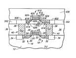
- a first semiconductor structure 10is illustrated in fragmentary view.
- Structure 10comprises a monocrystalline semiconductor substrate 12 .
- Substrate 12can comprise, for example, a monocrystalline silicon wafer.
- substrate 12can comprise other semiconductive materials besides, or in addition to, silicon, including, for example, germanium.
- Monocrystalline substrate 12can be background-doped with either a p-type or n-type dopant, and in the shown embodiment substrate 10 is illustrated to be n-type doped.
- n-type substrateis defined as a semiconductive substrate having a higher concentration of n-type dopant than p-type dopant (to the extent that any p-type dopant is present); and similarly a p-type semiconductive substrate is defined as a substrate having a higher concentration of p-type dopant than n-type dopant (to the extent that any p-type dopant is present).
- a “background” dopingis defined as a dopant provided throughout an entirety of a semiconductive material substrate to a concentration of less than 10 18 atoms/cm 3 .
- semiconductor substrateand “semiconductor substrate” are defined to mean any construction comprising semiconductive material, including, but not limited to, bulk semiconductive materials such as a semiconductive wafer (either alone or in assemblies comprising other materials thereon), and semiconductive material layers (either alone or in assemblies comprising other materials).
- substraterefers to any supporting structure, including, but not limited to, the semiconductive substrates described above.
- Structure 10can be referred to herein and in the claims that follow as a first semiconductor structure
- substrate 12can be referred to herein and in the claims that follow as a first monocrystalline semiconductor substrate.
- Transistor structure 14is formed to be supported by substrate 12 .
- Transistor structure 14comprises a transistor gate 16 and source/drain regions 18 .
- Transistor gate 16comprises a pad oxide layer 20 , a first conductive layer 22 , a second conductive layer 24 , and an insulative cap 26 .
- Pad oxide layer 20can comprise, for example, silicon dioxide.
- First conductive layer 22can comprise, for example, conductively-doped polysilicon.
- Second conductive layer 24can comprise, for example, a metal silicide, such as, for example, titanium silicide or tungsten silicide.
- Insulative cap 26can comprise, for example, silicon nitride or silicon dioxide.
- Sidewall spacers 28are formed along sidewalls of gate 16 , and can comprise, for example, silicon nitride or silicon dioxide.
- Source/drain regions 18comprise a lightly-doped region 30 and a heavily-doped region 32 .
- Regions 30 and 32can comprise either n-type or p-type dopant, and in the shown embodiment are p-type regions.
- Lightly-doped regions 30 and heavily-doped regions 32can be doped to typical concentrations utilized for forming conventional transistor structures.
- Isolation regions 34extend within semiconductive substrate 12 .
- Isolation regions 34can comprise, for example, silicon dioxide, and can be formed as, for example, shallow trench isolation regions.
- An insulative mass 36is formed over substrate 12 , and can comprise, for example, borophosphosilicate glass (BPSG).
- a pair of openingsextend through insulative mass 36 and are filled with conductive material 38 to define upwardly extending conductive projections 40 and 42 .
- Conductive material 38can comprise, for example, conductively doped silicon, such as conductively doped polysilicon.
- the polysiliconcan be either n-type or p-type doped, and in the shown embodiment is doped to be a p-type material.
- Conductively-doped material 38preferably comprises a same-type conductive doping as heavily-doped regions 32 .
- conductive material 38can preferably comprise n-type doped polysilicon.
- Conductive projections 40 and 42extend downwardly to substrate 12 , and connect with source/drain regions 18 of transistor assembly 14 . Conductive projections 40 and 42 thus electrically connect with electrical nodes supported by substrate 12 , (in the shown embodiment the electrical nodes are source/drain regions 18 ).
- electrical connectionis defined to not encompass selective or switched connections.
- conductive projection 40is to be understood as being in electrical connection with a source/drain region - 32 illustrated on the left of gate 16 , but to not be in electrical connection with a source/drain region 32 illustrated on the right of gate 16 .
- conductive projection 42is to be understood as being in electrical connection with a source/drain region 32 illustrated on the right of gate 16 , but to not be in electrical connection with a source/drain region 32 illustrated on the left of gate 16 .
- the plugs 40 and 42 of the FIG. 1 structureare shown to overlap isolation regions 34 , as well as overlapping source/drain regions 32 .
- the partial overlap of plugs 40 and 42 on isolation regions 34can allow formation of a relatively compact device. It is to be understood, however, that the invention encompasses other embodiments wherein at least one of the plugs 40 and 42 is entirely over a source/drain region 32 and does not overlap an isolation region 34 .
- Structure 10has an upper surface 44 that is preferably substantially planar.
- substantially planaris defined herein to refer to a surface defined by a roughness of less than 5 ⁇ root mean square (rms) variation, and more preferably less than 2 ⁇ rms variation.
- FIG. 2shows a second semiconductor structure 500 comprising a second monocrystalline semiconductor substrate 502 .
- Second monocrystalline semiconductor substrate 502can comprise, for example, monocrystalline silicon, and can be background-doped with n-type or p-type dopant.
- second monocrystalline substrate 502comprises monocrystalline semiconductive material (such as, for example, monocrystalline silicon) doped with p-type background dopant
- first monocrystalline substrate 12comprises monocrystalline semiconductive material (such as, for example, monocrystalline silicon) doped with n-type background dopant.
- second monocrystalline substrate 502is background doped with a different type of dopant than is first monocrystalline substrate 12 .
- Substrate 502comprises a damage region 504 formed therein.
- Damage region 504can be formed by, for example, implanting hydrogen ions into wafer 502 .
- Wafer 502has an upper surface 506 which is preferably substantially planar.
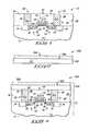
- second structure 500is inverted and bonded to first structure 10 to form a resulting structure 600 .
- surface 506 of substrate 502is bonded to surface 44 of substrate 10 .
- the bonding of substrate 502 to substrate 10can be accomplished with a temperature of less than or equal to about 700° C. for a time of at least about 15 minutes. A suitable time can be from about 15 minutes to about two hours.
- the bondingcan occur under a nitrogen atmosphere at about atmospheric pressure, or alternatively can occur under a vacuum.
- a suitable vacuumis less than or equal to about 500 mTorr, and preferably less than or equal to about 10 mTorr.
- the bondingcan comprise a first temperature treatment of less than 500° C., and a second temperature treatment of less than or equal to about 700° C.
- the treatment occurring at a temperature of less than about 500° C.can be utilized as a preliminary bonding prior to cleaving of substrate 502 (described below with reference to FIG. 4 ), and the bonding at 700° C. can occur after such cleaving to enhance chemical coupling between substrate 502 and upper surface 44 . of structure 10 .
- the only temperatures utilized for bondingare less than or equal to 700° C., and monocrystalline substrates 12 and 502 are not exposed to temperatures exceeding 700° C. after the bonding.
- An advantage of utilizing temperatures less than or equal to about 700° C. for bonding and subsequent processing of structure 600is that such could alleviate diffusion of dopants within substrates 12 and 502 relative to diffusion which would occur at higher temperatures.
- temperatures above 700° C.can be utilized for bonding substrate 502 to structure 10 .
- insulative mask 36comprises silicon dioxide
- such embodimentscan comprise temperatures high enough to bond the silicon dioxide of mass 36 to the monocrystalline silicon of base 502 , such as, for example, temperatures of 900° C. or greater.
- temperatures of 700° C. or lesscan be utilized to bond polycrystalline silicon conductive material 38 to base 502 , even though such temperatures will probably not effectively bond insulative material 36 to base 502 .
- substrate 502is cleaved along damage region 504 .
- damage region 504corresponds to a region wherein hydrogen ions were implanted
- the cleavagecan be accomplished by thermal processing. Suitable thermal processing can include, for example, exposure of damage region 504 to a temperature of greater than or equal to about 500° C.
- the cleavageleaves a roughened upper surface 602 of structure 600 .
- Such roughened surfacecan be planarized by, for example, chemical-mechanical planarization to form the planar upper surface 604 shown in FIG. 5 .
- the thickness of fragment 502 remaining after cleavage( FIG. 4 ) is about 0.5 ⁇ m
- the thickness after planarization( FIG. 5 ) is about 0.3 ⁇ m.
- the planarization shown in FIG. 5can be referred to as “smoothing” of the roughened upper surface 602 of the FIG. 4 structure 600 .
- a pair of insulative material regions 606 and 608are formed within monocrystalline substrate 502 .
- Regions 606 and 608can comprise, for example, silicon dioxide or silicon nitride. Regions 606 and 608 can be formed by, for example, etching trenches through substrate 502 , and subsequently refilling the trenches with silicon dioxide. It is noted that insulative region 606 entirely covers conductive projection 40 , while insulative region 608 only partially covers conductive projection 42 .
- Transistor structure 610is formed to be supported by second monocrystalline substrate 502 .
- Transistor structure 610comprises a transistor gate 612 and source/drain regions 614 .
- Transistor gate 612comprises a pad oxide 616 , a first conductive region 618 , a second conductive region 620 , and an insulative cap 622 .
- Pad oxide 616 , first conductive region 618 , second conductive region 620 and insulative cap 622can comprise the same materials as discussed above for pad oxide 20 , first conductive region 22 , second conductive region 24 , and insulative material 26 , respectively, of transistor gate 16 of FIG. 1.
- a pair of sidewall spacers 624are formed along sidewalls of transistor gate 612 . Sidewall spacers 624 can comprise, for example, silicon dioxide or silicon nitride.
- Source/drain regions 614comprise a lightly doped region 626 and a heavily doped region 628 .
- Regions 626 and 628can comprise either n-type dopant or p-type dopant.
- heavily-doped regions 628are n-type regions.
- Transistor structure 610can be formed by conventional methods, such as, for example, by forming transistor gate 612 over substrate 502 , and subsequently implanting dopant to form lightly-doped regions 626 within base 502 . Spacers 624 can then be formed adjacent gate 612 , followed by implanting dopant to form heavily doped regions 628 within base 502 .
- Insulative mass 630is formed over transistor structure 610 , as well as over base 502 .
- Insulative mass 630can comprise, for example, BPSG.
- Conductive interconnects 650 , 652 and 654are formed through insulative material 630 .
- Conductive interconnects 650 and 652can be referred to as first and second conductive interconnects, respectively, and interconnect 654 can be referred to as a third conductive interconnect.
- Conductive interconnects 650 and 652extend through base 502 to connect with conductive projections 40 and 42 , respectively.
- conductive interconnects 650 and 652comprise n-type doped semiconductive material
- conductive interconnects 40 and 42comprise p-type doped semiconductive material.
- Conductive interconnects 650 and 652can comprise, for example, n-type doped polycrystalline silicon.
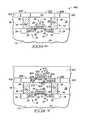
- Metal silicide layers 656 and 658are formed at interfaces of the n-type semiconductive material and p-type semiconductive material. The metal silicide can be formed by sputter deposition from a highly collimated source.
- Conductive interconnect 654is also shown to comprise n-type doped semiconductive material, but unlike conductive interconnects 650 and 652 , conductive interconnect 654 stops at an upper surface of monocrystalline base 502 .
- conductive interconnects 650 and 652would be formed in a separate etch step from conductive interconnect 654 , in that conductive interconnects 650 and 652 are etched through base 502 , while conductive interconnect 654 is not.
- the etch to form an opening for conductive interconnect 654is preferably highly selective for the material 630 relative to the materials 622 and 624 .
- material 630can comprise BPSG and materials 622 and 624 can comprise silicon nitride so that an etch highly selective for silicon oxide to silicon nitride is used to form the opening for interconnect 654 .
- the etchcan also be selective for silicon oxide relative to silicon if base 502 comprises monocrystalline silicon so that the etch stops at about an upper surface of base 502 .
- Conductive interconnect 654is shown having a metal silicide layer 660 at an interface between conductive interconnect 654 and heavily doped source/drain region 628 .
- the metal silicide 660is optional in the shown embodiment, since conductive interconnect 654 and source/drain region 628 both comprise the same conductivity type doping (specifically, n-type doping).
- Conductive interconnect 650 and projection 40together define a conductive extension 670 (which can also be referred to as a conductive interconnect), and likewise conductive interconnect 652 and projection 42 together define a conductive extension 672 (which can also be referred to as a conductive interconnect).
- Conductive extensions 670 and 672can be considered to comprise upper portions (either 650 or 652 ) and lower portions (either 40 or 42 ), with the upper portions having a different conductivity type than the lower portions.
- conductive extensions 670 and 672can be considered to comprise a metal silicide (either 656 or 658 ) at an interface of the upper portions and the lower portions.
- the metal silicidecan comprise, for example, titanium silicide.
- the upper portionsextend only partially through the substrate 502 , so that the metal silicide interface is within substrate 502 . It is to be understood that the invention encompasses other embodiments in which the upper portions extend entirely through the second monocrystalline semiconductive substrate (see, for example, FIG. 10 for an exemplary embodiment in which the upper portions extend entirely through a second monocrystalline semiconductive substrate).
- an n-type doped region 659is formed proximate conductive interconnect 652 by out-diffusion of n-type dopant from the interconnect into base 502 . Such out-diffusion can be accomplished by, for example, thermal processing of structure 600 . Doped region 659 can improve an electrical interconnection between conductive extension 652 and an adjacent source/drain region 628 .
- FIG. 8The structure of FIG. 8 is shown incorporated into logic circuitry. Specifically, conductive interconnect 650 is shown joined to a conductive connection 680 , which joins with V cc ; conductive interconnect 652 is shown joined with a conductive connection 682 which joins with an output of a logic device, and conductive interconnect 654 is shown joined with a conductive connection 684 that is connected to ground.
- the structures 670 , 672 and 654 of FIG. 8are shown in a common plane to simplify illustration of such structures. It is to be understood that the invention can be practiced with one or more of structures 670 , 672 and 654 in a different cross-sectional plane relative to the other structures.
- FIG. 9illustrates a circuit diagram of a logic device which can incorporate the circuitry shown in FIG. 8 .
- the circuitry of FIG. 9constitutes what is known in the art as a “logic inverter”. As can be seen in the diagram of FIG. 9 , there would be an input (not shown in FIG. 8 ) feeding into transistor gate regions 16 and 612 . Such input can be considered as being out of the shown cross-sectional plane of FIG. 8 , and can comprise, for example, a conductive component perpendicular to the shown cross-sectional plane of FIG. 8 .
- FIG. 8is but one type of logic device that can be formed utilizing methodology of the present invention.
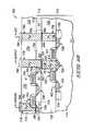
- FIGS. 10 and 11illustrate another type of logic device that can be formed, with the logic device of FIGS. 10 and 11 being a so-called NAND gate logic structure.
- FIG. 10illustrates a structure 700 comprising a first structure 710 and a second structure 712 bonded thereto.
- Structure 710is analogous to the structure 10 of FIG. 1 , and comprises a first monocrystalline semiconductor substrate 714 ; and structure 712 is analogous to the second semiconductor structure 500 of FIG. 2 , and comprises a second monocrystalline semiconductor substrate 716 .
- First monocrystalline substrate 714can comprise, for example, monocrystalline silicon doped with a background n-type dopant, and second monocrystalline substrate 716 can comprise monocrystalline silicon background doped with a p-type dopant.
- Structure 710comprises transistor structures 720 and 722 supported by substrate 714 .
- Transistor structures 720 and 722comprise transistor gates 721 and 723 , and source/drain regions 724 , 726 , and 728 adjacent the transistor gates.
- Isolation regions 730are formed within substrate 714 , and can comprise, for example, shallow trench isolation regions.
- Insulative mass 732is formed over transistor structures 720 and 722 , as well as over first monocrystalline substrate 714 .
- Insulative mass 732can comprise, for example, BPSG.
- Conductive projections 734 and 736extend through insulative mass 732 to electrically connected with electrical nodes supported by substrate 714 (specifically, to electrically connect with source/drain regions 726 and 728 ), and in shown embodiment physically contact substrate 714 .
- Conductive projections 734 and 736comprise a conductive material 738 , such as, for example, conductively doped polycrystalline silicon. In the shown embodiment, conductive material 738 is p-type doped.
- second structure 712can be bonded to first structure 710 utilizing processing analogous to that described above with reference to FIGS. 1-5 .
- second structure 712can initially comprise a monocrystalline substrate having a damage region formed therein. The monocrystalline substrate can be bonded to first semiconductive structure 710 , and subsequently cleaved along the damage region and planarized.
- an oxide region 750can be formed within monocrystalline material 716 .
- transistor structures 752 and 754can be formed to be supported by monocrystalline substrate 716 .
- Transistor structures 752 and 754comprise source/drain regions 756 , 758 and 760 proximate transistor gates 753 and 755 .
- An insulative mass 770is formed over transistor structures 752 and 754 , as well as over monocrystalline substrate 716 . Subsequently, conductive extensions 776 , 778 and 780 are formed to extend through insulative mass 770 .
- Conductive extension 776terminates on monocrystalline substrate 712 at source/drain region 756 , whereas conductive extensions 778 and 780 extend through monocrystalline substrate 712 to connect with projections 734 and 736 , respectively.
- Conductive extensions 776 , 778 and 780are shown to comprise conductively-doped semiconductive material, and specifically are shown to comprise n-type doped conductive material. Extensions 776 , 778 and 780 can comprise, for example, n-type doped polysilicon.
- Metal silicide regions 782 and 784are shown at interfaces of n-type doped semiconductive material and p-type doped semiconductive material. Also, a metal silicide region 786 is shown at an interface of conductive extension 776 and source/drain region 756 .
- Metal silicide regions 782 , 784 and 786can comprise, for example, titanium silicide, cobalt silicide, tungsten silicide, or other refractory silicides.
- the regionscan comprise refractory metal nitrides, such as, for example, titanium nitride.
- An out-diffused dopant region 759is shown adjacent extension 778 , and can be formed by methodology similar to that described above with reference to FIG. 8 for forming region 659 .
- Conductive extension 776is shown joined to a conductive contact 790 , which ultimately connects with ground; conductive interconnect 778 is shown in connection with a conductive contact 792 which ultimately connects with output; and conductive interconnect 780 is shown in electrical connection with a conductive contact 794 which ultimately connects with V cc .
- FIG. 11shows a circuit diagram of the NAND device of FIG. 10 .
- FIG. 11also illustrates that there would be a pair of inputs going into the device of FIG. 10 which are not shown in the diagram of FIG. 10 .
- the inputscould, for example, comprise electrical connections extending into and out of the shown cross-sectional plane of FIG. 10 .
- FIG. 11shows that there are electrical connections between transistor gates 752 and 720 , as well as between transistor gates 754 and 722 . Such electrical connections can extend outside of the shown cross-sectional plane of FIG. 10 .
- the cross-sectional plane illustrated in FIG. 10is shown for diagrammatic purposes only. In practice, one or more of the structures shown in the cross-sectional plane of FIG. 10 can be formed in a different plane relative to other structures illustrated in the cross-sectional plane of FIG. 10 , as will be understood by persons of ordinary skill in the art.
Landscapes
- Engineering & Computer Science (AREA)
- Microelectronics & Electronic Packaging (AREA)
- Power Engineering (AREA)
- Physics & Mathematics (AREA)
- Condensed Matter Physics & Semiconductors (AREA)
- General Physics & Mathematics (AREA)
- Computer Hardware Design (AREA)
- Manufacturing & Machinery (AREA)
- Metal-Oxide And Bipolar Metal-Oxide Semiconductor Integrated Circuits (AREA)
- Insulated Gate Type Field-Effect Transistor (AREA)
- Internal Circuitry In Semiconductor Integrated Circuit Devices (AREA)
- Electrodes Of Semiconductors (AREA)
Abstract
Description
Claims (5)
Priority Applications (2)
| Application Number | Priority Date | Filing Date | Title |
|---|---|---|---|
| US10/931,569US6927431B2 (en) | 2001-02-28 | 2004-08-31 | Semiconductor circuit constructions |
| US11/092,029US7115451B2 (en) | 2001-02-28 | 2005-03-29 | Methods of forming semiconductor circuitry |
Applications Claiming Priority (2)
| Application Number | Priority Date | Filing Date | Title |
|---|---|---|---|
| US09/797,098US6887753B2 (en) | 2001-02-28 | 2001-02-28 | Methods of forming semiconductor circuitry, and semiconductor circuit constructions |
| US10/931,569US6927431B2 (en) | 2001-02-28 | 2004-08-31 | Semiconductor circuit constructions |
Related Parent Applications (1)
| Application Number | Title | Priority Date | Filing Date |
|---|---|---|---|
| US09/797,098ContinuationUS6887753B2 (en) | 2001-02-28 | 2001-02-28 | Methods of forming semiconductor circuitry, and semiconductor circuit constructions |
Related Child Applications (1)
| Application Number | Title | Priority Date | Filing Date |
|---|---|---|---|
| US11/092,029DivisionUS7115451B2 (en) | 2001-02-28 | 2005-03-29 | Methods of forming semiconductor circuitry |
Publications (2)
| Publication Number | Publication Date |
|---|---|
| US20050042821A1 US20050042821A1 (en) | 2005-02-24 |
| US6927431B2true US6927431B2 (en) | 2005-08-09 |
Family
ID=25169900
Family Applications (7)
| Application Number | Title | Priority Date | Filing Date |
|---|---|---|---|
| US09/797,098Expired - LifetimeUS6887753B2 (en) | 2001-02-28 | 2001-02-28 | Methods of forming semiconductor circuitry, and semiconductor circuit constructions |
| US10/931,579Expired - LifetimeUS6964896B2 (en) | 2001-02-28 | 2004-08-31 | Methods of forming semiconductor logic circuitry, and semiconductor logic circuit constructions |
| US10/931,567Expired - LifetimeUS7151041B2 (en) | 2001-02-28 | 2004-08-31 | Methods of forming semiconductor circuitry |
| US10/931,569Expired - LifetimeUS6927431B2 (en) | 2001-02-28 | 2004-08-31 | Semiconductor circuit constructions |
| US11/092,029Expired - LifetimeUS7115451B2 (en) | 2001-02-28 | 2005-03-29 | Methods of forming semiconductor circuitry |
| US11/346,985Expired - LifetimeUS7250680B2 (en) | 2001-02-28 | 2006-02-02 | Semiconductor circuitry constructions |
| US11/395,721Expired - LifetimeUS7326960B2 (en) | 2001-02-28 | 2006-03-31 | Semiconductor circuit constructions |
Family Applications Before (3)
| Application Number | Title | Priority Date | Filing Date |
|---|---|---|---|
| US09/797,098Expired - LifetimeUS6887753B2 (en) | 2001-02-28 | 2001-02-28 | Methods of forming semiconductor circuitry, and semiconductor circuit constructions |
| US10/931,579Expired - LifetimeUS6964896B2 (en) | 2001-02-28 | 2004-08-31 | Methods of forming semiconductor logic circuitry, and semiconductor logic circuit constructions |
| US10/931,567Expired - LifetimeUS7151041B2 (en) | 2001-02-28 | 2004-08-31 | Methods of forming semiconductor circuitry |
Family Applications After (3)
| Application Number | Title | Priority Date | Filing Date |
|---|---|---|---|
| US11/092,029Expired - LifetimeUS7115451B2 (en) | 2001-02-28 | 2005-03-29 | Methods of forming semiconductor circuitry |
| US11/346,985Expired - LifetimeUS7250680B2 (en) | 2001-02-28 | 2006-02-02 | Semiconductor circuitry constructions |
| US11/395,721Expired - LifetimeUS7326960B2 (en) | 2001-02-28 | 2006-03-31 | Semiconductor circuit constructions |
Country Status (1)
| Country | Link |
|---|---|
| US (7) | US6887753B2 (en) |
Cited By (196)
| Publication number | Priority date | Publication date | Assignee | Title |
|---|---|---|---|---|
| US20090258462A1 (en)* | 2004-09-29 | 2009-10-15 | Konevecki Michael W | Method for forming doped polysilicon via connecting polysilicon layers |
| US20100035429A1 (en)* | 2007-01-18 | 2010-02-11 | Terasemicon Corporation | Method for fabricating semiconductor device |
| US20110199116A1 (en)* | 2010-02-16 | 2011-08-18 | NuPGA Corporation | Method for fabrication of a semiconductor device and structure |
| US20130095580A1 (en)* | 2011-10-18 | 2013-04-18 | Zvi Or-Bach | Semiconductor device and structure |
| US20140061810A1 (en)* | 2012-09-05 | 2014-03-06 | Renesas Electronics Corporation | Semiconductor device and manufacturing method thereof |
| US8753913B2 (en) | 2010-10-13 | 2014-06-17 | Monolithic 3D Inc. | Method for fabricating novel semiconductor and optoelectronic devices |
| US8803206B1 (en) | 2012-12-29 | 2014-08-12 | Monolithic 3D Inc. | 3D semiconductor device and structure |
| US8836073B1 (en) | 2012-04-09 | 2014-09-16 | Monolithic 3D Inc. | Semiconductor device and structure |
| US8901613B2 (en) | 2011-03-06 | 2014-12-02 | Monolithic 3D Inc. | Semiconductor device and structure for heat removal |
| US8902663B1 (en) | 2013-03-11 | 2014-12-02 | Monolithic 3D Inc. | Method of maintaining a memory state |
| US8907442B2 (en) | 2009-10-12 | 2014-12-09 | Monolthic 3D Inc. | System comprising a semiconductor device and structure |
| US8912052B2 (en) | 2010-07-30 | 2014-12-16 | Monolithic 3D Inc. | Semiconductor device and structure |
| US8921970B1 (en) | 2012-12-22 | 2014-12-30 | Monolithic 3D Inc | Semiconductor device and structure |
| US8956959B2 (en) | 2010-10-11 | 2015-02-17 | Monolithic 3D Inc. | Method of manufacturing a semiconductor device with two monocrystalline layers |
| US8975670B2 (en) | 2011-03-06 | 2015-03-10 | Monolithic 3D Inc. | Semiconductor device and structure for heat removal |
| US8987079B2 (en) | 2009-04-14 | 2015-03-24 | Monolithic 3D Inc. | Method for developing a custom device |
| US8994404B1 (en) | 2013-03-12 | 2015-03-31 | Monolithic 3D Inc. | Semiconductor device and structure |
| US9030858B2 (en) | 2011-10-02 | 2015-05-12 | Monolithic 3D Inc. | Semiconductor device and structure |
| US9099526B2 (en) | 2010-02-16 | 2015-08-04 | Monolithic 3D Inc. | Integrated circuit device and structure |
| US9099424B1 (en) | 2012-08-10 | 2015-08-04 | Monolithic 3D Inc. | Semiconductor system, device and structure with heat removal |
| US9117749B1 (en) | 2013-03-15 | 2015-08-25 | Monolithic 3D Inc. | Semiconductor device and structure |
| US9197804B1 (en) | 2011-10-14 | 2015-11-24 | Monolithic 3D Inc. | Semiconductor and optoelectronic devices |
| US9219005B2 (en) | 2011-06-28 | 2015-12-22 | Monolithic 3D Inc. | Semiconductor system and device |
| US9412645B1 (en) | 2009-04-14 | 2016-08-09 | Monolithic 3D Inc. | Semiconductor devices and structures |
| US9509313B2 (en) | 2009-04-14 | 2016-11-29 | Monolithic 3D Inc. | 3D semiconductor device |
| US9577642B2 (en) | 2009-04-14 | 2017-02-21 | Monolithic 3D Inc. | Method to form a 3D semiconductor device |
| US9871034B1 (en) | 2012-12-29 | 2018-01-16 | Monolithic 3D Inc. | Semiconductor device and structure |
| US9953925B2 (en) | 2011-06-28 | 2018-04-24 | Monolithic 3D Inc. | Semiconductor system and device |
| US10043781B2 (en) | 2009-10-12 | 2018-08-07 | Monolithic 3D Inc. | 3D semiconductor device and structure |
| US10115663B2 (en) | 2012-12-29 | 2018-10-30 | Monolithic 3D Inc. | 3D semiconductor device and structure |
| US10127344B2 (en) | 2013-04-15 | 2018-11-13 | Monolithic 3D Inc. | Automation for monolithic 3D devices |
| US10157909B2 (en) | 2009-10-12 | 2018-12-18 | Monolithic 3D Inc. | 3D semiconductor device and structure |
| US10217667B2 (en) | 2011-06-28 | 2019-02-26 | Monolithic 3D Inc. | 3D semiconductor device, fabrication method and system |
| US10224279B2 (en) | 2013-03-15 | 2019-03-05 | Monolithic 3D Inc. | Semiconductor device and structure |
| US10290682B2 (en) | 2010-10-11 | 2019-05-14 | Monolithic 3D Inc. | 3D IC semiconductor device and structure with stacked memory |
| US10297586B2 (en) | 2015-03-09 | 2019-05-21 | Monolithic 3D Inc. | Methods for processing a 3D semiconductor device |
| US10325651B2 (en) | 2013-03-11 | 2019-06-18 | Monolithic 3D Inc. | 3D semiconductor device with stacked memory |
| US10354995B2 (en) | 2009-10-12 | 2019-07-16 | Monolithic 3D Inc. | Semiconductor memory device and structure |
| US10366970B2 (en) | 2009-10-12 | 2019-07-30 | Monolithic 3D Inc. | 3D semiconductor device and structure |
| US10381328B2 (en) | 2015-04-19 | 2019-08-13 | Monolithic 3D Inc. | Semiconductor device and structure |
| US10388568B2 (en) | 2011-06-28 | 2019-08-20 | Monolithic 3D Inc. | 3D semiconductor device and system |
| US10388863B2 (en) | 2009-10-12 | 2019-08-20 | Monolithic 3D Inc. | 3D memory device and structure |
| US10418369B2 (en) | 2015-10-24 | 2019-09-17 | Monolithic 3D Inc. | Multi-level semiconductor memory device and structure |
| US10497713B2 (en) | 2010-11-18 | 2019-12-03 | Monolithic 3D Inc. | 3D semiconductor memory device and structure |
| US10515981B2 (en) | 2015-09-21 | 2019-12-24 | Monolithic 3D Inc. | Multilevel semiconductor device and structure with memory |
| US10522225B1 (en) | 2015-10-02 | 2019-12-31 | Monolithic 3D Inc. | Semiconductor device with non-volatile memory |
| US10600888B2 (en) | 2012-04-09 | 2020-03-24 | Monolithic 3D Inc. | 3D semiconductor device |
| US10600657B2 (en) | 2012-12-29 | 2020-03-24 | Monolithic 3D Inc | 3D semiconductor device and structure |
| US10651054B2 (en) | 2012-12-29 | 2020-05-12 | Monolithic 3D Inc. | 3D semiconductor device and structure |
| US10679977B2 (en) | 2010-10-13 | 2020-06-09 | Monolithic 3D Inc. | 3D microdisplay device and structure |
| US10825779B2 (en) | 2015-04-19 | 2020-11-03 | Monolithic 3D Inc. | 3D semiconductor device and structure |
| US10833108B2 (en) | 2010-10-13 | 2020-11-10 | Monolithic 3D Inc. | 3D microdisplay device and structure |
| US10840239B2 (en) | 2014-08-26 | 2020-11-17 | Monolithic 3D Inc. | 3D semiconductor device and structure |
| US10847540B2 (en) | 2015-10-24 | 2020-11-24 | Monolithic 3D Inc. | 3D semiconductor memory device and structure |
| US10892169B2 (en) | 2012-12-29 | 2021-01-12 | Monolithic 3D Inc. | 3D semiconductor device and structure |
| US10892016B1 (en) | 2019-04-08 | 2021-01-12 | Monolithic 3D Inc. | 3D memory semiconductor devices and structures |
| US10896931B1 (en) | 2010-10-11 | 2021-01-19 | Monolithic 3D Inc. | 3D semiconductor device and structure |
| US10903089B1 (en) | 2012-12-29 | 2021-01-26 | Monolithic 3D Inc. | 3D semiconductor device and structure |
| US10910364B2 (en) | 2009-10-12 | 2021-02-02 | Monolitaic 3D Inc. | 3D semiconductor device |
| US10943934B2 (en) | 2010-10-13 | 2021-03-09 | Monolithic 3D Inc. | Multilevel semiconductor device and structure |
| US10978501B1 (en) | 2010-10-13 | 2021-04-13 | Monolithic 3D Inc. | Multilevel semiconductor device and structure with waveguides |
| US10998374B1 (en) | 2010-10-13 | 2021-05-04 | Monolithic 3D Inc. | Multilevel semiconductor device and structure |
| US11004719B1 (en) | 2010-11-18 | 2021-05-11 | Monolithic 3D Inc. | Methods for producing a 3D semiconductor memory device and structure |
| US11004694B1 (en) | 2012-12-29 | 2021-05-11 | Monolithic 3D Inc. | 3D semiconductor device and structure |
| US11011507B1 (en) | 2015-04-19 | 2021-05-18 | Monolithic 3D Inc. | 3D semiconductor device and structure |
| US11018191B1 (en) | 2010-10-11 | 2021-05-25 | Monolithic 3D Inc. | 3D semiconductor device and structure |
| US11018042B1 (en) | 2010-11-18 | 2021-05-25 | Monolithic 3D Inc. | 3D semiconductor memory device and structure |
| US11018156B2 (en) | 2019-04-08 | 2021-05-25 | Monolithic 3D Inc. | 3D memory semiconductor devices and structures |
| US11018116B2 (en) | 2012-12-22 | 2021-05-25 | Monolithic 3D Inc. | Method to form a 3D semiconductor device and structure |
| US11018133B2 (en) | 2009-10-12 | 2021-05-25 | Monolithic 3D Inc. | 3D integrated circuit |
| US11024673B1 (en) | 2010-10-11 | 2021-06-01 | Monolithic 3D Inc. | 3D semiconductor device and structure |
| US11031275B2 (en) | 2010-11-18 | 2021-06-08 | Monolithic 3D Inc. | 3D semiconductor device and structure with memory |
| US11031394B1 (en) | 2014-01-28 | 2021-06-08 | Monolithic 3D Inc. | 3D semiconductor device and structure |
| US11030371B2 (en) | 2013-04-15 | 2021-06-08 | Monolithic 3D Inc. | Automation for monolithic 3D devices |
| US11043523B1 (en) | 2010-10-13 | 2021-06-22 | Monolithic 3D Inc. | Multilevel semiconductor device and structure with image sensors |
| US11056468B1 (en) | 2015-04-19 | 2021-07-06 | Monolithic 3D Inc. | 3D semiconductor device and structure |
| US11063024B1 (en) | 2012-12-22 | 2021-07-13 | Monlithic 3D Inc. | Method to form a 3D semiconductor device and structure |
| US11063071B1 (en) | 2010-10-13 | 2021-07-13 | Monolithic 3D Inc. | Multilevel semiconductor device and structure with waveguides |
| US11087995B1 (en) | 2012-12-29 | 2021-08-10 | Monolithic 3D Inc. | 3D semiconductor device and structure |
| US11088130B2 (en) | 2014-01-28 | 2021-08-10 | Monolithic 3D Inc. | 3D semiconductor device and structure |
| US11088050B2 (en) | 2012-04-09 | 2021-08-10 | Monolithic 3D Inc. | 3D semiconductor device with isolation layers |
| US11094576B1 (en) | 2010-11-18 | 2021-08-17 | Monolithic 3D Inc. | Methods for producing a 3D semiconductor memory device and structure |
| US11107721B2 (en) | 2010-11-18 | 2021-08-31 | Monolithic 3D Inc. | 3D semiconductor device and structure with NAND logic |
| US11107808B1 (en) | 2014-01-28 | 2021-08-31 | Monolithic 3D Inc. | 3D semiconductor device and structure |
| US11114427B2 (en) | 2015-11-07 | 2021-09-07 | Monolithic 3D Inc. | 3D semiconductor processor and memory device and structure |
| US11114464B2 (en) | 2015-10-24 | 2021-09-07 | Monolithic 3D Inc. | 3D semiconductor device and structure |
| US11121021B2 (en) | 2010-11-18 | 2021-09-14 | Monolithic 3D Inc. | 3D semiconductor device and structure |
| US11133344B2 (en) | 2010-10-13 | 2021-09-28 | Monolithic 3D Inc. | Multilevel semiconductor device and structure with image sensors |
| US11158674B2 (en) | 2010-10-11 | 2021-10-26 | Monolithic 3D Inc. | Method to produce a 3D semiconductor device and structure |
| US11158652B1 (en) | 2019-04-08 | 2021-10-26 | Monolithic 3D Inc. | 3D memory semiconductor devices and structures |
| US11164898B2 (en) | 2010-10-13 | 2021-11-02 | Monolithic 3D Inc. | Multilevel semiconductor device and structure |
| US11164811B2 (en) | 2012-04-09 | 2021-11-02 | Monolithic 3D Inc. | 3D semiconductor device with isolation layers and oxide-to-oxide bonding |
| US11163112B2 (en) | 2010-10-13 | 2021-11-02 | Monolithic 3D Inc. | Multilevel semiconductor device and structure with electromagnetic modulators |
| US11164770B1 (en) | 2010-11-18 | 2021-11-02 | Monolithic 3D Inc. | Method for producing a 3D semiconductor memory device and structure |
| US11177140B2 (en) | 2012-12-29 | 2021-11-16 | Monolithic 3D Inc. | 3D semiconductor device and structure |
| US11211279B2 (en) | 2010-11-18 | 2021-12-28 | Monolithic 3D Inc. | Method for processing a 3D integrated circuit and structure |
| US11217565B2 (en) | 2012-12-22 | 2022-01-04 | Monolithic 3D Inc. | Method to form a 3D semiconductor device and structure |
| US11227897B2 (en) | 2010-10-11 | 2022-01-18 | Monolithic 3D Inc. | Method for producing a 3D semiconductor memory device and structure |
| US11251149B2 (en) | 2016-10-10 | 2022-02-15 | Monolithic 3D Inc. | 3D memory device and structure |
| US11257867B1 (en) | 2010-10-11 | 2022-02-22 | Monolithic 3D Inc. | 3D semiconductor device and structure with oxide bonds |
| US11270055B1 (en) | 2013-04-15 | 2022-03-08 | Monolithic 3D Inc. | Automation for monolithic 3D devices |
| US11296115B1 (en) | 2015-10-24 | 2022-04-05 | Monolithic 3D Inc. | 3D semiconductor device and structure |
| US11296106B2 (en) | 2019-04-08 | 2022-04-05 | Monolithic 3D Inc. | 3D memory semiconductor devices and structures |
| US11309292B2 (en) | 2012-12-22 | 2022-04-19 | Monolithic 3D Inc. | 3D semiconductor device and structure with metal layers |
| US11315980B1 (en) | 2010-10-11 | 2022-04-26 | Monolithic 3D Inc. | 3D semiconductor device and structure with transistors |
| US11327227B2 (en) | 2010-10-13 | 2022-05-10 | Monolithic 3D Inc. | Multilevel semiconductor device and structure with electromagnetic modulators |
| US11329059B1 (en) | 2016-10-10 | 2022-05-10 | Monolithic 3D Inc. | 3D memory devices and structures with thinned single crystal substrates |
| US11341309B1 (en) | 2013-04-15 | 2022-05-24 | Monolithic 3D Inc. | Automation for monolithic 3D devices |
| US11355381B2 (en) | 2010-11-18 | 2022-06-07 | Monolithic 3D Inc. | 3D semiconductor memory device and structure |
| US11355380B2 (en) | 2010-11-18 | 2022-06-07 | Monolithic 3D Inc. | Methods for producing 3D semiconductor memory device and structure utilizing alignment marks |
| US11374118B2 (en) | 2009-10-12 | 2022-06-28 | Monolithic 3D Inc. | Method to form a 3D integrated circuit |
| US11398569B2 (en) | 2013-03-12 | 2022-07-26 | Monolithic 3D Inc. | 3D semiconductor device and structure |
| US11404466B2 (en) | 2010-10-13 | 2022-08-02 | Monolithic 3D Inc. | Multilevel semiconductor device and structure with image sensors |
| US11410912B2 (en) | 2012-04-09 | 2022-08-09 | Monolithic 3D Inc. | 3D semiconductor device with vias and isolation layers |
| US11430667B2 (en) | 2012-12-29 | 2022-08-30 | Monolithic 3D Inc. | 3D semiconductor device and structure with bonding |
| US11430668B2 (en) | 2012-12-29 | 2022-08-30 | Monolithic 3D Inc. | 3D semiconductor device and structure with bonding |
| US11437368B2 (en) | 2010-10-13 | 2022-09-06 | Monolithic 3D Inc. | Multilevel semiconductor device and structure with oxide bonding |
| US11443971B2 (en) | 2010-11-18 | 2022-09-13 | Monolithic 3D Inc. | 3D semiconductor device and structure with memory |
| US11469271B2 (en) | 2010-10-11 | 2022-10-11 | Monolithic 3D Inc. | Method to produce 3D semiconductor devices and structures with memory |
| US11476181B1 (en) | 2012-04-09 | 2022-10-18 | Monolithic 3D Inc. | 3D semiconductor device and structure with metal layers |
| US11482438B2 (en) | 2010-11-18 | 2022-10-25 | Monolithic 3D Inc. | Methods for producing a 3D semiconductor memory device and structure |
| US11482440B2 (en) | 2010-12-16 | 2022-10-25 | Monolithic 3D Inc. | 3D semiconductor device and structure with a built-in test circuit for repairing faulty circuits |
| US11482439B2 (en) | 2010-11-18 | 2022-10-25 | Monolithic 3D Inc. | Methods for producing a 3D semiconductor memory device comprising charge trap junction-less transistors |
| US11487928B2 (en) | 2013-04-15 | 2022-11-01 | Monolithic 3D Inc. | Automation for monolithic 3D devices |
| US11495484B2 (en) | 2010-11-18 | 2022-11-08 | Monolithic 3D Inc. | 3D semiconductor devices and structures with at least two single-crystal layers |
| US11508605B2 (en) | 2010-11-18 | 2022-11-22 | Monolithic 3D Inc. | 3D semiconductor memory device and structure |
| US11521888B2 (en) | 2010-11-18 | 2022-12-06 | Monolithic 3D Inc. | 3D semiconductor device and structure with high-k metal gate transistors |
| US11569117B2 (en) | 2010-11-18 | 2023-01-31 | Monolithic 3D Inc. | 3D semiconductor device and structure with single-crystal layers |
| US11574109B1 (en) | 2013-04-15 | 2023-02-07 | Monolithic 3D Inc | Automation methods for 3D integrated circuits and devices |
| US11594473B2 (en) | 2012-04-09 | 2023-02-28 | Monolithic 3D Inc. | 3D semiconductor device and structure with metal layers and a connective path |
| US11600667B1 (en) | 2010-10-11 | 2023-03-07 | Monolithic 3D Inc. | Method to produce 3D semiconductor devices and structures with memory |
| US11605663B2 (en) | 2010-10-13 | 2023-03-14 | Monolithic 3D Inc. | Multilevel semiconductor device and structure with image sensors and wafer bonding |
| US11610802B2 (en) | 2010-11-18 | 2023-03-21 | Monolithic 3D Inc. | Method for producing a 3D semiconductor device and structure with single crystal transistors and metal gate electrodes |
| US11616004B1 (en) | 2012-04-09 | 2023-03-28 | Monolithic 3D Inc. | 3D semiconductor device and structure with metal layers and a connective path |
| US11615977B2 (en) | 2010-11-18 | 2023-03-28 | Monolithic 3D Inc. | 3D semiconductor memory device and structure |
| US11694944B1 (en) | 2012-04-09 | 2023-07-04 | Monolithic 3D Inc. | 3D semiconductor device and structure with metal layers and a connective path |
| US11694922B2 (en) | 2010-10-13 | 2023-07-04 | Monolithic 3D Inc. | Multilevel semiconductor device and structure with oxide bonding |
| US11711928B2 (en) | 2016-10-10 | 2023-07-25 | Monolithic 3D Inc. | 3D memory devices and structures with control circuits |
| US11720736B2 (en) | 2013-04-15 | 2023-08-08 | Monolithic 3D Inc. | Automation methods for 3D integrated circuits and devices |
| US11735501B1 (en) | 2012-04-09 | 2023-08-22 | Monolithic 3D Inc. | 3D semiconductor device and structure with metal layers and a connective path |
| US11735462B2 (en) | 2010-11-18 | 2023-08-22 | Monolithic 3D Inc. | 3D semiconductor device and structure with single-crystal layers |
| US11763864B2 (en) | 2019-04-08 | 2023-09-19 | Monolithic 3D Inc. | 3D memory semiconductor devices and structures with bit-line pillars |
| US11784169B2 (en) | 2012-12-22 | 2023-10-10 | Monolithic 3D Inc. | 3D semiconductor device and structure with metal layers |
| US11784082B2 (en) | 2010-11-18 | 2023-10-10 | Monolithic 3D Inc. | 3D semiconductor device and structure with bonding |
| US11804396B2 (en) | 2010-11-18 | 2023-10-31 | Monolithic 3D Inc. | Methods for producing a 3D semiconductor device and structure with memory cells and multiple metal layers |
| US11812620B2 (en) | 2016-10-10 | 2023-11-07 | Monolithic 3D Inc. | 3D DRAM memory devices and structures with control circuits |
| US11855100B2 (en) | 2010-10-13 | 2023-12-26 | Monolithic 3D Inc. | Multilevel semiconductor device and structure with oxide bonding |
| US11854857B1 (en) | 2010-11-18 | 2023-12-26 | Monolithic 3D Inc. | Methods for producing a 3D semiconductor device and structure with memory cells and multiple metal layers |
| US11855114B2 (en) | 2010-10-13 | 2023-12-26 | Monolithic 3D Inc. | Multilevel semiconductor device and structure with image sensors and wafer bonding |
| US11862503B2 (en) | 2010-11-18 | 2024-01-02 | Monolithic 3D Inc. | Method for producing a 3D semiconductor device and structure with memory cells and multiple metal layers |
| US11869591B2 (en) | 2016-10-10 | 2024-01-09 | Monolithic 3D Inc. | 3D memory devices and structures with control circuits |
| US11869915B2 (en) | 2010-10-13 | 2024-01-09 | Monolithic 3D Inc. | Multilevel semiconductor device and structure with image sensors and wafer bonding |
| US11869965B2 (en) | 2013-03-11 | 2024-01-09 | Monolithic 3D Inc. | 3D semiconductor device and structure with metal layers and memory cells |
| US11881443B2 (en) | 2012-04-09 | 2024-01-23 | Monolithic 3D Inc. | 3D semiconductor device and structure with metal layers and a connective path |
| US11901210B2 (en) | 2010-11-18 | 2024-02-13 | Monolithic 3D Inc. | 3D semiconductor device and structure with memory |
| US11916045B2 (en) | 2012-12-22 | 2024-02-27 | Monolithic 3D Inc. | 3D semiconductor device and structure with metal layers |
| US11923374B2 (en) | 2013-03-12 | 2024-03-05 | Monolithic 3D Inc. | 3D semiconductor device and structure with metal layers |
| US11923230B1 (en) | 2010-11-18 | 2024-03-05 | Monolithic 3D Inc. | 3D semiconductor device and structure with bonding |
| US11929372B2 (en) | 2010-10-13 | 2024-03-12 | Monolithic 3D Inc. | Multilevel semiconductor device and structure with image sensors and wafer bonding |
| US11930648B1 (en) | 2016-10-10 | 2024-03-12 | Monolithic 3D Inc. | 3D memory devices and structures with metal layers |
| US11937422B2 (en) | 2015-11-07 | 2024-03-19 | Monolithic 3D Inc. | Semiconductor memory device and structure |
| US11935949B1 (en) | 2013-03-11 | 2024-03-19 | Monolithic 3D Inc. | 3D semiconductor device and structure with metal layers and memory cells |
| US11956952B2 (en) | 2015-08-23 | 2024-04-09 | Monolithic 3D Inc. | Semiconductor memory device and structure |
| US11961827B1 (en) | 2012-12-22 | 2024-04-16 | Monolithic 3D Inc. | 3D semiconductor device and structure with metal layers |
| US11967583B2 (en) | 2012-12-22 | 2024-04-23 | Monolithic 3D Inc. | 3D semiconductor device and structure with metal layers |
| US11978731B2 (en) | 2015-09-21 | 2024-05-07 | Monolithic 3D Inc. | Method to produce a multi-level semiconductor memory device and structure |
| US11984445B2 (en) | 2009-10-12 | 2024-05-14 | Monolithic 3D Inc. | 3D semiconductor devices and structures with metal layers |
| US11984438B2 (en) | 2010-10-13 | 2024-05-14 | Monolithic 3D Inc. | Multilevel semiconductor device and structure with oxide bonding |
| US11991884B1 (en) | 2015-10-24 | 2024-05-21 | Monolithic 3D Inc. | 3D semiconductor device and structure with logic and memory |
| US12016181B2 (en) | 2015-10-24 | 2024-06-18 | Monolithic 3D Inc. | 3D semiconductor device and structure with logic and memory |
| US12027518B1 (en) | 2009-10-12 | 2024-07-02 | Monolithic 3D Inc. | 3D semiconductor devices and structures with metal layers |
| US12035531B2 (en) | 2015-10-24 | 2024-07-09 | Monolithic 3D Inc. | 3D semiconductor device and structure with logic and memory |
| US12033884B2 (en) | 2010-11-18 | 2024-07-09 | Monolithic 3D Inc. | Methods for producing a 3D semiconductor device and structure with memory cells and multiple metal layers |
| US12051674B2 (en) | 2012-12-22 | 2024-07-30 | Monolithic 3D Inc. | 3D semiconductor device and structure with metal layers |
| US12068187B2 (en) | 2010-11-18 | 2024-08-20 | Monolithic 3D Inc. | 3D semiconductor device and structure with bonding and DRAM memory cells |
| US12080743B2 (en) | 2010-10-13 | 2024-09-03 | Monolithic 3D Inc. | Multilevel semiconductor device and structure with image sensors and wafer bonding |
| US12094892B2 (en) | 2010-10-13 | 2024-09-17 | Monolithic 3D Inc. | 3D micro display device and structure |
| US12094965B2 (en) | 2013-03-11 | 2024-09-17 | Monolithic 3D Inc. | 3D semiconductor device and structure with metal layers and memory cells |
| US12094829B2 (en) | 2014-01-28 | 2024-09-17 | Monolithic 3D Inc. | 3D semiconductor device and structure |
| US12100658B2 (en) | 2015-09-21 | 2024-09-24 | Monolithic 3D Inc. | Method to produce a 3D multilayer semiconductor device and structure |
| US12100611B2 (en) | 2010-11-18 | 2024-09-24 | Monolithic 3D Inc. | Methods for producing a 3D semiconductor device and structure with memory cells and multiple metal layers |
| US12100646B2 (en) | 2013-03-12 | 2024-09-24 | Monolithic 3D Inc. | 3D semiconductor device and structure with metal layers |
| US12120880B1 (en) | 2015-10-24 | 2024-10-15 | Monolithic 3D Inc. | 3D semiconductor device and structure with logic and memory |
| US12125737B1 (en) | 2010-11-18 | 2024-10-22 | Monolithic 3D Inc. | 3D semiconductor device and structure with metal layers and memory cells |
| US12136562B2 (en) | 2010-11-18 | 2024-11-05 | Monolithic 3D Inc. | 3D semiconductor device and structure with single-crystal layers |
| US12144190B2 (en) | 2010-11-18 | 2024-11-12 | Monolithic 3D Inc. | 3D semiconductor device and structure with bonding and memory cells preliminary class |
| US12154817B1 (en) | 2010-11-18 | 2024-11-26 | Monolithic 3D Inc. | Methods for producing a 3D semiconductor memory device and structure |
| US12178055B2 (en) | 2015-09-21 | 2024-12-24 | Monolithic 3D Inc. | 3D semiconductor memory devices and structures |
| US12219769B2 (en) | 2015-10-24 | 2025-02-04 | Monolithic 3D Inc. | 3D semiconductor device and structure with logic and memory |
| US12225704B2 (en) | 2016-10-10 | 2025-02-11 | Monolithic 3D Inc. | 3D memory devices and structures with memory arrays and metal layers |
| US12243765B2 (en) | 2010-11-18 | 2025-03-04 | Monolithic 3D Inc. | 3D semiconductor device and structure with metal layers and memory cells |
| US12249538B2 (en) | 2012-12-29 | 2025-03-11 | Monolithic 3D Inc. | 3D semiconductor device and structure including power distribution grids |
| US12250830B2 (en) | 2015-09-21 | 2025-03-11 | Monolithic 3D Inc. | 3D semiconductor memory devices and structures |
| US12272586B2 (en) | 2010-11-18 | 2025-04-08 | Monolithic 3D Inc. | 3D semiconductor memory device and structure with memory and metal layers |
| US12360310B2 (en) | 2010-10-13 | 2025-07-15 | Monolithic 3D Inc. | Multilevel semiconductor device and structure with oxide bonding |
| US12362219B2 (en) | 2010-11-18 | 2025-07-15 | Monolithic 3D Inc. | 3D semiconductor memory device and structure |
Families Citing this family (53)
| Publication number | Priority date | Publication date | Assignee | Title |
|---|---|---|---|---|
| US6635552B1 (en)* | 2000-06-12 | 2003-10-21 | Micron Technology, Inc. | Methods of forming semiconductor constructions |
| SG148819A1 (en)* | 2000-09-14 | 2009-01-29 | Semiconductor Energy Lab | Semiconductor device and manufacturing method thereof |
| US6972448B2 (en)* | 2000-12-31 | 2005-12-06 | Texas Instruments Incorporated | Sub-lithographics opening for back contact or back gate |
| US6887753B2 (en)* | 2001-02-28 | 2005-05-03 | Micron Technology, Inc. | Methods of forming semiconductor circuitry, and semiconductor circuit constructions |
| KR100553682B1 (en)* | 2003-03-07 | 2006-02-24 | 삼성전자주식회사 | A semiconductor device having a gate electrode and a method of forming the same |
| US6900667B2 (en)* | 2003-03-11 | 2005-05-31 | Micron Technology, Inc. | Logic constructions and electronic devices |
| JP4041785B2 (en)* | 2003-09-26 | 2008-01-30 | 松下電器産業株式会社 | Manufacturing method of semiconductor device |
| US6967149B2 (en)* | 2003-11-20 | 2005-11-22 | Hewlett-Packard Development Company, L.P. | Storage structure with cleaved layer |
| KR100574957B1 (en)* | 2003-11-21 | 2006-04-28 | 삼성전자주식회사 | Vertically stacked multi-board integrated circuit device and manufacturing method thereof |
| US7315466B2 (en)* | 2004-08-04 | 2008-01-01 | Samsung Electronics Co., Ltd. | Semiconductor memory device and method for arranging and manufacturing the same |
| KR100612418B1 (en)* | 2004-09-24 | 2006-08-16 | 삼성전자주식회사 | Semiconductor device having self-aligned body and manufacturing method thereof |
| US7179719B2 (en)* | 2004-09-28 | 2007-02-20 | Sharp Laboratories Of America, Inc. | System and method for hydrogen exfoliation |
| JP4583878B2 (en)* | 2004-10-29 | 2010-11-17 | 富士通セミコンダクター株式会社 | Manufacturing method of semiconductor device |
| JP4435057B2 (en)* | 2004-12-08 | 2010-03-17 | セイコーエプソン株式会社 | Semiconductor device and manufacturing method thereof |
| KR100702012B1 (en)* | 2005-03-22 | 2007-03-30 | 삼성전자주식회사 | S with landfill patterns. RAMs and Forming Methods |
| JP2006310741A (en)* | 2005-03-30 | 2006-11-09 | Seiko Epson Corp | Semiconductor device manufacturing method and semiconductor device |
| KR100621633B1 (en)* | 2005-04-18 | 2006-09-19 | 삼성전자주식회사 | Method of forming a semiconductor device having stacked transisters and the device so formed |
| KR100663360B1 (en)* | 2005-04-20 | 2007-01-02 | 삼성전자주식회사 | Semiconductor Devices Having Thin Film Transistors and Manufacturing Methods Thereof |
| KR100607413B1 (en)* | 2005-04-27 | 2006-08-01 | 삼성전자주식회사 | Stacked semiconductor device and method of manufacturing the same |
| DE102006015975B4 (en)* | 2005-06-09 | 2008-12-18 | Samsung Electronics Co., Ltd., Suwon | Multi-level semiconductor devices and method of making the same |
| KR100715267B1 (en)* | 2005-06-09 | 2007-05-08 | 삼성전자주식회사 | Stacked semiconductor device and manufacturing method thereof |
| US7978561B2 (en)* | 2005-07-28 | 2011-07-12 | Samsung Electronics Co., Ltd. | Semiconductor memory devices having vertically-stacked transistors therein |
| US20090224330A1 (en)* | 2005-07-28 | 2009-09-10 | Hong Chang Min | Semiconductor Memory Device and Method for Arranging and Manufacturing the Same |
| WO2007089206A1 (en)* | 2006-02-01 | 2007-08-09 | Silex Microsystems Ab | Vias and method of making |
| KR100706807B1 (en)* | 2006-02-03 | 2007-04-12 | 삼성전자주식회사 | Stacked transistors having protruding impurity regions and manufacturing method thereof |
| KR100714401B1 (en)* | 2006-02-08 | 2007-05-04 | 삼성전자주식회사 | A semiconductor device having a stacked transistor and a method of forming the same |
| KR101214901B1 (en)* | 2006-02-09 | 2012-12-26 | 삼성전자주식회사 | Multi-level semiconductor deivce |
| US20070194450A1 (en)* | 2006-02-21 | 2007-08-23 | Tyberg Christy S | BEOL compatible FET structure |
| KR100840785B1 (en)* | 2007-02-16 | 2008-06-23 | 삼성전자주식회사 | A method of forming a single crystal silicon pattern in a stacked semiconductor device. |
| US8049253B2 (en) | 2007-07-11 | 2011-11-01 | Semiconductor Energy Laboratory Co., Ltd. | Semiconductor device and method for manufacturing the same |
| KR100960451B1 (en)* | 2008-02-29 | 2010-05-28 | 주식회사 하이닉스반도체 | Semiconductor device and manufacturing method thereof |
| KR100991220B1 (en) | 2008-07-21 | 2010-11-04 | 삼성전자주식회사 | Contact structure in a substrate having an bonded interface, a semiconductor device having the same and methods of manufacturing the same |
| JP5043788B2 (en)* | 2008-09-18 | 2012-10-10 | ダンロップスポーツ株式会社 | Golf ball |
| JP5201048B2 (en)* | 2009-03-25 | 2013-06-05 | 富士通株式会社 | Semiconductor device and manufacturing method thereof |
| TWI579995B (en)* | 2009-08-19 | 2017-04-21 | Xintex Inc | Chip package and method of manufacturing same |
| EP2491585B1 (en)* | 2009-10-21 | 2020-01-22 | Semiconductor Energy Laboratory Co. Ltd. | Semiconductor device |
| WO2012008304A1 (en)* | 2010-07-16 | 2012-01-19 | Semiconductor Energy Laboratory Co., Ltd. | Semiconductor device |
| US20120248621A1 (en)* | 2011-03-31 | 2012-10-04 | S.O.I.Tec Silicon On Insulator Technologies | Methods of forming bonded semiconductor structures, and semiconductor structures formed by such methods |
| US8338294B2 (en) | 2011-03-31 | 2012-12-25 | Soitec | Methods of forming bonded semiconductor structures including two or more processed semiconductor structures carried by a common substrate, and semiconductor structures formed by such methods |
| JP6019599B2 (en) | 2011-03-31 | 2016-11-02 | ソニー株式会社 | Semiconductor device and manufacturing method thereof |
| US9269858B2 (en)* | 2011-08-31 | 2016-02-23 | Micron Technology, Inc. | Engineered substrates for semiconductor devices and associated systems and methods |
| CN103367353A (en)* | 2012-03-30 | 2013-10-23 | 东莞万士达液晶显示器有限公司 | Active components and active component array substrates |
| TWI566328B (en)* | 2013-07-29 | 2017-01-11 | 高效電源轉換公司 | Gallium nitride transistor having a polysilicon layer for generating additional components |
| WO2015155656A1 (en)* | 2014-04-11 | 2015-10-15 | Semiconductor Energy Laboratory Co., Ltd. | Semiconductor device and electronic device |
| US9087689B1 (en) | 2014-07-11 | 2015-07-21 | Inoso, Llc | Method of forming a stacked low temperature transistor and related devices |
| FR3042910B1 (en)* | 2015-10-27 | 2018-03-09 | Commissariat A L'energie Atomique Et Aux Energies Alternatives | INTERCONNECTIONS BASED ON SEMICONDUCTOR ALLOY AND METAL FOR 3D CIRCUIT |
| US10109582B2 (en)* | 2016-04-19 | 2018-10-23 | Taiwan Semiconductor Manufacturing Company Limited | Advanced metal connection with metal cut |
| US11011537B2 (en)* | 2016-09-30 | 2021-05-18 | Intel Corporation | Vertical interconnect methods for stacked device architectures using direct self assembly with high operational parallelization and improved scalability |
| DE112017008080T5 (en)* | 2017-12-26 | 2020-07-09 | Intel Corporation | STACKED TRANSISTORS WITH LAST TRAINED CONTACT |
| US11430814B2 (en) | 2018-03-05 | 2022-08-30 | Intel Corporation | Metallization structures for stacked device connectivity and their methods of fabrication |
| US11348916B2 (en)* | 2018-06-29 | 2022-05-31 | Intel Corporation | Leave-behind protective layer having secondary purpose |
| US12148757B2 (en)* | 2019-04-22 | 2024-11-19 | Intel Corporation | Integration of Si-based transistors with non-Si technologies by semiconductor regrowth over an insulator material |
| TWI870393B (en)* | 2020-03-17 | 2025-01-21 | 聯華電子股份有限公司 | Semiconductor device and method for fabricating the same |
Citations (13)
| Publication number | Priority date | Publication date | Assignee | Title |
|---|---|---|---|---|
| US5374581A (en) | 1991-07-31 | 1994-12-20 | Canon Kabushiki Kaisha | Method for preparing semiconductor member |
| US5953622A (en) | 1996-11-23 | 1999-09-14 | Hyundai Electronics Industries Co., Ltd. | Method for fabricating semiconductor wafers |
| US6187624B1 (en) | 1999-06-04 | 2001-02-13 | Taiwan Semiconductor Manufacturing Company | Method for making closely spaced capacitors with reduced parasitic capacitance on a dynamic random access memory (DRAM) device |
| US6245661B1 (en) | 1990-05-31 | 2001-06-12 | Canon Kabushiki Kaisha | Method of producing a wiring for a semiconductor circuit |
| US6251754B1 (en) | 1997-05-09 | 2001-06-26 | Denso Corporation | Semiconductor substrate manufacturing method |
| US6255160B1 (en) | 1999-10-29 | 2001-07-03 | Taiwan Semiconductor Manufacturing Company | Cell design and process for making dynamic random access memory (DRAM) having one or more Gigabits of memory cells |
| US6423992B2 (en) | 1997-12-19 | 2002-07-23 | Hitachi, Ltd. | Semiconductor integrated circuit device |
| US6429070B1 (en) | 2000-08-30 | 2002-08-06 | Micron Technology, Inc. | DRAM cell constructions, and methods of forming DRAM cells |
| US6437369B1 (en)* | 1995-12-06 | 2002-08-20 | Micron Technology, Inc. | Method of forming dynamic random access memory circuitry and dynamic random access memory |
| US6462817B1 (en) | 2000-05-12 | 2002-10-08 | Carlos Strocchia-Rivera | Method of monitoring ion implants by examination of an overlying masking material |
| US6635552B1 (en) | 2000-06-12 | 2003-10-21 | Micron Technology, Inc. | Methods of forming semiconductor constructions |
| US6645846B2 (en)* | 2001-10-24 | 2003-11-11 | Micron Technology, Inc. | Methods of forming conductive contacts to conductive structures |
| US6740583B2 (en)* | 1998-08-27 | 2004-05-25 | Micron Technology, Inc. | Semiconductor processing methods of forming integrated circuitry and semiconductor processing methods of forming dynamic random access memory (DRAM) circuitry |
Family Cites Families (21)
| Publication number | Priority date | Publication date | Assignee | Title |
|---|---|---|---|---|
| EP0056186A3 (en) | 1981-01-08 | 1983-07-20 | Texas Instruments Incorporated | Integrated circuit device with interconnect-level logic diodes |
| US5006913A (en)* | 1988-11-05 | 1991-04-09 | Mitsubishi Denki Kabushiki Kaisha | Stacked type semiconductor device |
| EP0543361B1 (en)* | 1991-11-20 | 2002-02-27 | Canon Kabushiki Kaisha | Method of manufacturing a semiconductor device |
| US5334861A (en)* | 1992-05-19 | 1994-08-02 | Motorola Inc. | Semiconductor memory cell |
| US5612552A (en)* | 1994-03-31 | 1997-03-18 | Lsi Logic Corporation | Multilevel gate array integrated circuit structure with perpendicular access to all active device regions |
| US5834341A (en) | 1995-11-07 | 1998-11-10 | Winbond Electronics Corporation | Process for fabricating low off current thin film transistor |
| US5943775A (en)* | 1995-11-13 | 1999-08-31 | Qb Technology | Synthetic panel and method |
| US6653733B1 (en)* | 1996-02-23 | 2003-11-25 | Micron Technology, Inc. | Conductors in semiconductor devices |
| US5834354A (en) | 1996-11-07 | 1998-11-10 | Advanced Micro Devices, Inc. | Ultra high density NOR gate using a stacked transistor arrangement |
| SG65697A1 (en)* | 1996-11-15 | 1999-06-22 | Canon Kk | Process for producing semiconductor article |
| JP3153781B2 (en)* | 1997-06-02 | 2001-04-09 | 松下電送システム株式会社 | Relay communication device and relay communication method |
| JP4330670B2 (en)* | 1997-06-06 | 2009-09-16 | 株式会社東芝 | Nonvolatile semiconductor memory device |
| US5888872A (en) | 1997-06-20 | 1999-03-30 | Advanced Micro Devices, Inc. | Method for forming source drain junction areas self-aligned between a sidewall spacer and an etched lateral sidewall |
| US5818069A (en)* | 1997-06-20 | 1998-10-06 | Advanced Micro Devices, Inc. | Ultra high density series-connected transistors formed on separate elevational levels |
| JP3995830B2 (en)* | 1999-01-13 | 2007-10-24 | 富士フイルム株式会社 | Thermally developed image recording material |
| JP4807894B2 (en)* | 1999-05-31 | 2011-11-02 | ルネサスエレクトロニクス株式会社 | Semiconductor device |
| TW459275B (en)* | 1999-07-06 | 2001-10-11 | Semiconductor Energy Lab | Semiconductor device and method of fabricating the same |
| US6429484B1 (en)* | 2000-08-07 | 2002-08-06 | Advanced Micro Devices, Inc. | Multiple active layer structure and a method of making such a structure |
| JP2002184879A (en)* | 2000-12-19 | 2002-06-28 | Hitachi Ltd | Semiconductor device and method of manufacturing the same |
| US6887753B2 (en)* | 2001-02-28 | 2005-05-03 | Micron Technology, Inc. | Methods of forming semiconductor circuitry, and semiconductor circuit constructions |
| US6882010B2 (en)* | 2002-10-03 | 2005-04-19 | Micron Technology, Inc. | High performance three-dimensional TFT-based CMOS inverters, and computer systems utilizing such novel CMOS inverters |
- 2001
- 2001-02-28USUS09/797,098patent/US6887753B2/ennot_activeExpired - Lifetime
- 2004
- 2004-08-31USUS10/931,579patent/US6964896B2/ennot_activeExpired - Lifetime
- 2004-08-31USUS10/931,567patent/US7151041B2/ennot_activeExpired - Lifetime
- 2004-08-31USUS10/931,569patent/US6927431B2/ennot_activeExpired - Lifetime
- 2005
- 2005-03-29USUS11/092,029patent/US7115451B2/ennot_activeExpired - Lifetime
- 2006
- 2006-02-02USUS11/346,985patent/US7250680B2/ennot_activeExpired - Lifetime
- 2006-03-31USUS11/395,721patent/US7326960B2/ennot_activeExpired - Lifetime
Patent Citations (15)
| Publication number | Priority date | Publication date | Assignee | Title |
|---|---|---|---|---|
| US6245661B1 (en) | 1990-05-31 | 2001-06-12 | Canon Kabushiki Kaisha | Method of producing a wiring for a semiconductor circuit |
| US5374581A (en) | 1991-07-31 | 1994-12-20 | Canon Kabushiki Kaisha | Method for preparing semiconductor member |
| US6437369B1 (en)* | 1995-12-06 | 2002-08-20 | Micron Technology, Inc. | Method of forming dynamic random access memory circuitry and dynamic random access memory |
| US5953622A (en) | 1996-11-23 | 1999-09-14 | Hyundai Electronics Industries Co., Ltd. | Method for fabricating semiconductor wafers |
| US6251754B1 (en) | 1997-05-09 | 2001-06-26 | Denso Corporation | Semiconductor substrate manufacturing method |
| US6423992B2 (en) | 1997-12-19 | 2002-07-23 | Hitachi, Ltd. | Semiconductor integrated circuit device |
| US6740583B2 (en)* | 1998-08-27 | 2004-05-25 | Micron Technology, Inc. | Semiconductor processing methods of forming integrated circuitry and semiconductor processing methods of forming dynamic random access memory (DRAM) circuitry |
| US6187624B1 (en) | 1999-06-04 | 2001-02-13 | Taiwan Semiconductor Manufacturing Company | Method for making closely spaced capacitors with reduced parasitic capacitance on a dynamic random access memory (DRAM) device |
| US6255160B1 (en) | 1999-10-29 | 2001-07-03 | Taiwan Semiconductor Manufacturing Company | Cell design and process for making dynamic random access memory (DRAM) having one or more Gigabits of memory cells |
| US6462817B1 (en) | 2000-05-12 | 2002-10-08 | Carlos Strocchia-Rivera | Method of monitoring ion implants by examination of an overlying masking material |
| US6635552B1 (en) | 2000-06-12 | 2003-10-21 | Micron Technology, Inc. | Methods of forming semiconductor constructions |
| US6638834B2 (en) | 2000-06-12 | 2003-10-28 | Micron Technology, Inc. | Methods of forming semiconductor constructions |
| US6429070B1 (en) | 2000-08-30 | 2002-08-06 | Micron Technology, Inc. | DRAM cell constructions, and methods of forming DRAM cells |
| US6734062B2 (en) | 2000-08-30 | 2004-05-11 | Micron Technology, Inc. | Methods of forming DRAM cells |
| US6645846B2 (en)* | 2001-10-24 | 2003-11-11 | Micron Technology, Inc. | Methods of forming conductive contacts to conductive structures |
Cited By (222)
| Publication number | Priority date | Publication date | Assignee | Title |
|---|---|---|---|---|
| US20110021019A1 (en)* | 2004-09-29 | 2011-01-27 | Konevecki Michael W | Method for forming doped polysilicon via connecting polysilicon layers |
| US7915164B2 (en) | 2004-09-29 | 2011-03-29 | Sandisk 3D Llc | Method for forming doped polysilicon via connecting polysilicon layers |
| US7915163B2 (en)* | 2004-09-29 | 2011-03-29 | Sandisk 3D Llc | Method for forming doped polysilicon via connecting polysilicon layers |
| US20090258462A1 (en)* | 2004-09-29 | 2009-10-15 | Konevecki Michael W | Method for forming doped polysilicon via connecting polysilicon layers |
| US20100035429A1 (en)* | 2007-01-18 | 2010-02-11 | Terasemicon Corporation | Method for fabricating semiconductor device |
| US7928008B2 (en)* | 2007-01-18 | 2011-04-19 | Terasemicon Corporation | Method for fabricating semiconductor device |
| US9577642B2 (en) | 2009-04-14 | 2017-02-21 | Monolithic 3D Inc. | Method to form a 3D semiconductor device |
| US9412645B1 (en) | 2009-04-14 | 2016-08-09 | Monolithic 3D Inc. | Semiconductor devices and structures |
| US8987079B2 (en) | 2009-04-14 | 2015-03-24 | Monolithic 3D Inc. | Method for developing a custom device |
| US9509313B2 (en) | 2009-04-14 | 2016-11-29 | Monolithic 3D Inc. | 3D semiconductor device |
| US10043781B2 (en) | 2009-10-12 | 2018-08-07 | Monolithic 3D Inc. | 3D semiconductor device and structure |
| US12027518B1 (en) | 2009-10-12 | 2024-07-02 | Monolithic 3D Inc. | 3D semiconductor devices and structures with metal layers |
| US11018133B2 (en) | 2009-10-12 | 2021-05-25 | Monolithic 3D Inc. | 3D integrated circuit |
| US11984445B2 (en) | 2009-10-12 | 2024-05-14 | Monolithic 3D Inc. | 3D semiconductor devices and structures with metal layers |
| US10910364B2 (en) | 2009-10-12 | 2021-02-02 | Monolitaic 3D Inc. | 3D semiconductor device |
| US8907442B2 (en) | 2009-10-12 | 2014-12-09 | Monolthic 3D Inc. | System comprising a semiconductor device and structure |
| US9406670B1 (en) | 2009-10-12 | 2016-08-02 | Monolithic 3D Inc. | System comprising a semiconductor device and structure |
| US10388863B2 (en) | 2009-10-12 | 2019-08-20 | Monolithic 3D Inc. | 3D memory device and structure |
| US10354995B2 (en) | 2009-10-12 | 2019-07-16 | Monolithic 3D Inc. | Semiconductor memory device and structure |
| US10157909B2 (en) | 2009-10-12 | 2018-12-18 | Monolithic 3D Inc. | 3D semiconductor device and structure |
| US10366970B2 (en) | 2009-10-12 | 2019-07-30 | Monolithic 3D Inc. | 3D semiconductor device and structure |
| US11374118B2 (en) | 2009-10-12 | 2022-06-28 | Monolithic 3D Inc. | Method to form a 3D integrated circuit |
| US9564432B2 (en) | 2010-02-16 | 2017-02-07 | Monolithic 3D Inc. | 3D semiconductor device and structure |
| US9099526B2 (en) | 2010-02-16 | 2015-08-04 | Monolithic 3D Inc. | Integrated circuit device and structure |
| US20110199116A1 (en)* | 2010-02-16 | 2011-08-18 | NuPGA Corporation | Method for fabrication of a semiconductor device and structure |
| US8912052B2 (en) | 2010-07-30 | 2014-12-16 | Monolithic 3D Inc. | Semiconductor device and structure |
| US9419031B1 (en) | 2010-10-07 | 2016-08-16 | Monolithic 3D Inc. | Semiconductor and optoelectronic devices |
| US11018191B1 (en) | 2010-10-11 | 2021-05-25 | Monolithic 3D Inc. | 3D semiconductor device and structure |
| US8956959B2 (en) | 2010-10-11 | 2015-02-17 | Monolithic 3D Inc. | Method of manufacturing a semiconductor device with two monocrystalline layers |
| US11600667B1 (en) | 2010-10-11 | 2023-03-07 | Monolithic 3D Inc. | Method to produce 3D semiconductor devices and structures with memory |
| US11158674B2 (en) | 2010-10-11 | 2021-10-26 | Monolithic 3D Inc. | Method to produce a 3D semiconductor device and structure |
| US10896931B1 (en) | 2010-10-11 | 2021-01-19 | Monolithic 3D Inc. | 3D semiconductor device and structure |
| US10290682B2 (en) | 2010-10-11 | 2019-05-14 | Monolithic 3D Inc. | 3D IC semiconductor device and structure with stacked memory |
| US9818800B2 (en) | 2010-10-11 | 2017-11-14 | Monolithic 3D Inc. | Self aligned semiconductor device and structure |
| US11227897B2 (en) | 2010-10-11 | 2022-01-18 | Monolithic 3D Inc. | Method for producing a 3D semiconductor memory device and structure |
| US11257867B1 (en) | 2010-10-11 | 2022-02-22 | Monolithic 3D Inc. | 3D semiconductor device and structure with oxide bonds |
| US11469271B2 (en) | 2010-10-11 | 2022-10-11 | Monolithic 3D Inc. | Method to produce 3D semiconductor devices and structures with memory |
| US11024673B1 (en) | 2010-10-11 | 2021-06-01 | Monolithic 3D Inc. | 3D semiconductor device and structure |
| US11315980B1 (en) | 2010-10-11 | 2022-04-26 | Monolithic 3D Inc. | 3D semiconductor device and structure with transistors |
| US11327227B2 (en) | 2010-10-13 | 2022-05-10 | Monolithic 3D Inc. | Multilevel semiconductor device and structure with electromagnetic modulators |
| US12360310B2 (en) | 2010-10-13 | 2025-07-15 | Monolithic 3D Inc. | Multilevel semiconductor device and structure with oxide bonding |
| US11063071B1 (en) | 2010-10-13 | 2021-07-13 | Monolithic 3D Inc. | Multilevel semiconductor device and structure with waveguides |
| US11043523B1 (en) | 2010-10-13 | 2021-06-22 | Monolithic 3D Inc. | Multilevel semiconductor device and structure with image sensors |
| US11374042B1 (en) | 2010-10-13 | 2022-06-28 | Monolithic 3D Inc. | 3D micro display semiconductor device and structure |
| US11929372B2 (en) | 2010-10-13 | 2024-03-12 | Monolithic 3D Inc. | Multilevel semiconductor device and structure with image sensors and wafer bonding |
| US11164898B2 (en) | 2010-10-13 | 2021-11-02 | Monolithic 3D Inc. | Multilevel semiconductor device and structure |
| US10998374B1 (en) | 2010-10-13 | 2021-05-04 | Monolithic 3D Inc. | Multilevel semiconductor device and structure |
| US11133344B2 (en) | 2010-10-13 | 2021-09-28 | Monolithic 3D Inc. | Multilevel semiconductor device and structure with image sensors |
| US10978501B1 (en) | 2010-10-13 | 2021-04-13 | Monolithic 3D Inc. | Multilevel semiconductor device and structure with waveguides |
| US11869915B2 (en) | 2010-10-13 | 2024-01-09 | Monolithic 3D Inc. | Multilevel semiconductor device and structure with image sensors and wafer bonding |
| US8823122B2 (en) | 2010-10-13 | 2014-09-02 | Monolithic 3D Inc. | Semiconductor and optoelectronic devices |
| US10943934B2 (en) | 2010-10-13 | 2021-03-09 | Monolithic 3D Inc. | Multilevel semiconductor device and structure |
| US11984438B2 (en) | 2010-10-13 | 2024-05-14 | Monolithic 3D Inc. | Multilevel semiconductor device and structure with oxide bonding |
| US11404466B2 (en) | 2010-10-13 | 2022-08-02 | Monolithic 3D Inc. | Multilevel semiconductor device and structure with image sensors |
| US11855114B2 (en) | 2010-10-13 | 2023-12-26 | Monolithic 3D Inc. | Multilevel semiconductor device and structure with image sensors and wafer bonding |
| US12080743B2 (en) | 2010-10-13 | 2024-09-03 | Monolithic 3D Inc. | Multilevel semiconductor device and structure with image sensors and wafer bonding |
| US8753913B2 (en) | 2010-10-13 | 2014-06-17 | Monolithic 3D Inc. | Method for fabricating novel semiconductor and optoelectronic devices |
| US11855100B2 (en) | 2010-10-13 | 2023-12-26 | Monolithic 3D Inc. | Multilevel semiconductor device and structure with oxide bonding |
| US12094892B2 (en) | 2010-10-13 | 2024-09-17 | Monolithic 3D Inc. | 3D micro display device and structure |
| US11437368B2 (en) | 2010-10-13 | 2022-09-06 | Monolithic 3D Inc. | Multilevel semiconductor device and structure with oxide bonding |
| US10833108B2 (en) | 2010-10-13 | 2020-11-10 | Monolithic 3D Inc. | 3D microdisplay device and structure |
| US11163112B2 (en) | 2010-10-13 | 2021-11-02 | Monolithic 3D Inc. | Multilevel semiconductor device and structure with electromagnetic modulators |
| US11605663B2 (en) | 2010-10-13 | 2023-03-14 | Monolithic 3D Inc. | Multilevel semiconductor device and structure with image sensors and wafer bonding |
| US10679977B2 (en) | 2010-10-13 | 2020-06-09 | Monolithic 3D Inc. | 3D microdisplay device and structure |
| US11694922B2 (en) | 2010-10-13 | 2023-07-04 | Monolithic 3D Inc. | Multilevel semiconductor device and structure with oxide bonding |
| US11482438B2 (en) | 2010-11-18 | 2022-10-25 | Monolithic 3D Inc. | Methods for producing a 3D semiconductor memory device and structure |
| US11018042B1 (en) | 2010-11-18 | 2021-05-25 | Monolithic 3D Inc. | 3D semiconductor memory device and structure |
| US11615977B2 (en) | 2010-11-18 | 2023-03-28 | Monolithic 3D Inc. | 3D semiconductor memory device and structure |
| US11610802B2 (en) | 2010-11-18 | 2023-03-21 | Monolithic 3D Inc. | Method for producing a 3D semiconductor device and structure with single crystal transistors and metal gate electrodes |
| US10497713B2 (en) | 2010-11-18 | 2019-12-03 | Monolithic 3D Inc. | 3D semiconductor memory device and structure |
| US11784082B2 (en) | 2010-11-18 | 2023-10-10 | Monolithic 3D Inc. | 3D semiconductor device and structure with bonding |
| US12362219B2 (en) | 2010-11-18 | 2025-07-15 | Monolithic 3D Inc. | 3D semiconductor memory device and structure |
| US11804396B2 (en) | 2010-11-18 | 2023-10-31 | Monolithic 3D Inc. | Methods for producing a 3D semiconductor device and structure with memory cells and multiple metal layers |
| US11569117B2 (en) | 2010-11-18 | 2023-01-31 | Monolithic 3D Inc. | 3D semiconductor device and structure with single-crystal layers |
| US11521888B2 (en) | 2010-11-18 | 2022-12-06 | Monolithic 3D Inc. | 3D semiconductor device and structure with high-k metal gate transistors |
| US11508605B2 (en) | 2010-11-18 | 2022-11-22 | Monolithic 3D Inc. | 3D semiconductor memory device and structure |
| US11854857B1 (en) | 2010-11-18 | 2023-12-26 | Monolithic 3D Inc. | Methods for producing a 3D semiconductor device and structure with memory cells and multiple metal layers |
| US11495484B2 (en) | 2010-11-18 | 2022-11-08 | Monolithic 3D Inc. | 3D semiconductor devices and structures with at least two single-crystal layers |
| US11862503B2 (en) | 2010-11-18 | 2024-01-02 | Monolithic 3D Inc. | Method for producing a 3D semiconductor device and structure with memory cells and multiple metal layers |
| US12272586B2 (en) | 2010-11-18 | 2025-04-08 | Monolithic 3D Inc. | 3D semiconductor memory device and structure with memory and metal layers |
| US11482439B2 (en) | 2010-11-18 | 2022-10-25 | Monolithic 3D Inc. | Methods for producing a 3D semiconductor memory device comprising charge trap junction-less transistors |
| US11901210B2 (en) | 2010-11-18 | 2024-02-13 | Monolithic 3D Inc. | 3D semiconductor device and structure with memory |
| US11121021B2 (en) | 2010-11-18 | 2021-09-14 | Monolithic 3D Inc. | 3D semiconductor device and structure |
| US11004719B1 (en) | 2010-11-18 | 2021-05-11 | Monolithic 3D Inc. | Methods for producing a 3D semiconductor memory device and structure |
| US11164770B1 (en) | 2010-11-18 | 2021-11-02 | Monolithic 3D Inc. | Method for producing a 3D semiconductor memory device and structure |
| US11923230B1 (en) | 2010-11-18 | 2024-03-05 | Monolithic 3D Inc. | 3D semiconductor device and structure with bonding |
| US12033884B2 (en) | 2010-11-18 | 2024-07-09 | Monolithic 3D Inc. | Methods for producing a 3D semiconductor device and structure with memory cells and multiple metal layers |
| US12068187B2 (en) | 2010-11-18 | 2024-08-20 | Monolithic 3D Inc. | 3D semiconductor device and structure with bonding and DRAM memory cells |
| US11735462B2 (en) | 2010-11-18 | 2023-08-22 | Monolithic 3D Inc. | 3D semiconductor device and structure with single-crystal layers |
| US11443971B2 (en) | 2010-11-18 | 2022-09-13 | Monolithic 3D Inc. | 3D semiconductor device and structure with memory |
| US12100611B2 (en) | 2010-11-18 | 2024-09-24 | Monolithic 3D Inc. | Methods for producing a 3D semiconductor device and structure with memory cells and multiple metal layers |
| US11211279B2 (en) | 2010-11-18 | 2021-12-28 | Monolithic 3D Inc. | Method for processing a 3D integrated circuit and structure |
| US12243765B2 (en) | 2010-11-18 | 2025-03-04 | Monolithic 3D Inc. | 3D semiconductor device and structure with metal layers and memory cells |
| US11031275B2 (en) | 2010-11-18 | 2021-06-08 | Monolithic 3D Inc. | 3D semiconductor device and structure with memory |
| US12125737B1 (en) | 2010-11-18 | 2024-10-22 | Monolithic 3D Inc. | 3D semiconductor device and structure with metal layers and memory cells |
| US12136562B2 (en) | 2010-11-18 | 2024-11-05 | Monolithic 3D Inc. | 3D semiconductor device and structure with single-crystal layers |
| US11107721B2 (en) | 2010-11-18 | 2021-08-31 | Monolithic 3D Inc. | 3D semiconductor device and structure with NAND logic |
| US11094576B1 (en) | 2010-11-18 | 2021-08-17 | Monolithic 3D Inc. | Methods for producing a 3D semiconductor memory device and structure |
| US11355380B2 (en) | 2010-11-18 | 2022-06-07 | Monolithic 3D Inc. | Methods for producing 3D semiconductor memory device and structure utilizing alignment marks |
| US12144190B2 (en) | 2010-11-18 | 2024-11-12 | Monolithic 3D Inc. | 3D semiconductor device and structure with bonding and memory cells preliminary class |
| US11355381B2 (en) | 2010-11-18 | 2022-06-07 | Monolithic 3D Inc. | 3D semiconductor memory device and structure |
| US12154817B1 (en) | 2010-11-18 | 2024-11-26 | Monolithic 3D Inc. | Methods for producing a 3D semiconductor memory device and structure |
| US11482440B2 (en) | 2010-12-16 | 2022-10-25 | Monolithic 3D Inc. | 3D semiconductor device and structure with a built-in test circuit for repairing faulty circuits |
| US8975670B2 (en) | 2011-03-06 | 2015-03-10 | Monolithic 3D Inc. | Semiconductor device and structure for heat removal |
| US8901613B2 (en) | 2011-03-06 | 2014-12-02 | Monolithic 3D Inc. | Semiconductor device and structure for heat removal |
| US9219005B2 (en) | 2011-06-28 | 2015-12-22 | Monolithic 3D Inc. | Semiconductor system and device |
| US9953925B2 (en) | 2011-06-28 | 2018-04-24 | Monolithic 3D Inc. | Semiconductor system and device |
| US10217667B2 (en) | 2011-06-28 | 2019-02-26 | Monolithic 3D Inc. | 3D semiconductor device, fabrication method and system |
| US10388568B2 (en) | 2011-06-28 | 2019-08-20 | Monolithic 3D Inc. | 3D semiconductor device and system |
| US9030858B2 (en) | 2011-10-02 | 2015-05-12 | Monolithic 3D Inc. | Semiconductor device and structure |
| US9197804B1 (en) | 2011-10-14 | 2015-11-24 | Monolithic 3D Inc. | Semiconductor and optoelectronic devices |
| US9029173B2 (en)* | 2011-10-18 | 2015-05-12 | Monolithic 3D Inc. | Method for fabrication of a semiconductor device and structure |
| US20130095580A1 (en)* | 2011-10-18 | 2013-04-18 | Zvi Or-Bach | Semiconductor device and structure |
| US11735501B1 (en) | 2012-04-09 | 2023-08-22 | Monolithic 3D Inc. | 3D semiconductor device and structure with metal layers and a connective path |
| US11164811B2 (en) | 2012-04-09 | 2021-11-02 | Monolithic 3D Inc. | 3D semiconductor device with isolation layers and oxide-to-oxide bonding |
| US11088050B2 (en) | 2012-04-09 | 2021-08-10 | Monolithic 3D Inc. | 3D semiconductor device with isolation layers |
| US11476181B1 (en) | 2012-04-09 | 2022-10-18 | Monolithic 3D Inc. | 3D semiconductor device and structure with metal layers |
| US10600888B2 (en) | 2012-04-09 | 2020-03-24 | Monolithic 3D Inc. | 3D semiconductor device |
| US11410912B2 (en) | 2012-04-09 | 2022-08-09 | Monolithic 3D Inc. | 3D semiconductor device with vias and isolation layers |
| US11594473B2 (en) | 2012-04-09 | 2023-02-28 | Monolithic 3D Inc. | 3D semiconductor device and structure with metal layers and a connective path |
| US11616004B1 (en) | 2012-04-09 | 2023-03-28 | Monolithic 3D Inc. | 3D semiconductor device and structure with metal layers and a connective path |
| US8836073B1 (en) | 2012-04-09 | 2014-09-16 | Monolithic 3D Inc. | Semiconductor device and structure |
| US11881443B2 (en) | 2012-04-09 | 2024-01-23 | Monolithic 3D Inc. | 3D semiconductor device and structure with metal layers and a connective path |
| US9305867B1 (en) | 2012-04-09 | 2016-04-05 | Monolithic 3D Inc. | Semiconductor devices and structures |
| US11694944B1 (en) | 2012-04-09 | 2023-07-04 | Monolithic 3D Inc. | 3D semiconductor device and structure with metal layers and a connective path |
| US9099424B1 (en) | 2012-08-10 | 2015-08-04 | Monolithic 3D Inc. | Semiconductor system, device and structure with heat removal |
| US9680031B2 (en)* | 2012-09-05 | 2017-06-13 | Renesas Electronics Corporation | Semiconductor device and manufacturing method thereof |
| US20140061810A1 (en)* | 2012-09-05 | 2014-03-06 | Renesas Electronics Corporation | Semiconductor device and manufacturing method thereof |
| US9331071B2 (en)* | 2012-09-05 | 2016-05-03 | Renesas Electronics Corporation | Semiconductor device and manufacturing method thereof |
| US11309292B2 (en) | 2012-12-22 | 2022-04-19 | Monolithic 3D Inc. | 3D semiconductor device and structure with metal layers |
| US8921970B1 (en) | 2012-12-22 | 2014-12-30 | Monolithic 3D Inc | Semiconductor device and structure |
| US11961827B1 (en) | 2012-12-22 | 2024-04-16 | Monolithic 3D Inc. | 3D semiconductor device and structure with metal layers |
| US11063024B1 (en) | 2012-12-22 | 2021-07-13 | Monlithic 3D Inc. | Method to form a 3D semiconductor device and structure |
| US11784169B2 (en) | 2012-12-22 | 2023-10-10 | Monolithic 3D Inc. | 3D semiconductor device and structure with metal layers |
| US12051674B2 (en) | 2012-12-22 | 2024-07-30 | Monolithic 3D Inc. | 3D semiconductor device and structure with metal layers |
| US12278216B2 (en) | 2012-12-22 | 2025-04-15 | Monolithic 3D Inc. | 3D semiconductor device and structure with metal layers |
| US11217565B2 (en) | 2012-12-22 | 2022-01-04 | Monolithic 3D Inc. | Method to form a 3D semiconductor device and structure |
| US11916045B2 (en) | 2012-12-22 | 2024-02-27 | Monolithic 3D Inc. | 3D semiconductor device and structure with metal layers |
| US9252134B2 (en) | 2012-12-22 | 2016-02-02 | Monolithic 3D Inc. | Semiconductor device and structure |
| US11967583B2 (en) | 2012-12-22 | 2024-04-23 | Monolithic 3D Inc. | 3D semiconductor device and structure with metal layers |
| US11018116B2 (en) | 2012-12-22 | 2021-05-25 | Monolithic 3D Inc. | Method to form a 3D semiconductor device and structure |
| US11087995B1 (en) | 2012-12-29 | 2021-08-10 | Monolithic 3D Inc. | 3D semiconductor device and structure |
| US10600657B2 (en) | 2012-12-29 | 2020-03-24 | Monolithic 3D Inc | 3D semiconductor device and structure |
| US11430668B2 (en) | 2012-12-29 | 2022-08-30 | Monolithic 3D Inc. | 3D semiconductor device and structure with bonding |
| US11004694B1 (en) | 2012-12-29 | 2021-05-11 | Monolithic 3D Inc. | 3D semiconductor device and structure |
| US9460978B1 (en) | 2012-12-29 | 2016-10-04 | Monolithic 3D Inc. | Semiconductor device and structure |
| US10115663B2 (en) | 2012-12-29 | 2018-10-30 | Monolithic 3D Inc. | 3D semiconductor device and structure |
| US12249538B2 (en) | 2012-12-29 | 2025-03-11 | Monolithic 3D Inc. | 3D semiconductor device and structure including power distribution grids |
| US10903089B1 (en) | 2012-12-29 | 2021-01-26 | Monolithic 3D Inc. | 3D semiconductor device and structure |
| US9385058B1 (en) | 2012-12-29 | 2016-07-05 | Monolithic 3D Inc. | Semiconductor device and structure |
| US9460991B1 (en) | 2012-12-29 | 2016-10-04 | Monolithic 3D Inc. | Semiconductor device and structure |
| US10892169B2 (en) | 2012-12-29 | 2021-01-12 | Monolithic 3D Inc. | 3D semiconductor device and structure |
| US11430667B2 (en) | 2012-12-29 | 2022-08-30 | Monolithic 3D Inc. | 3D semiconductor device and structure with bonding |
| US8803206B1 (en) | 2012-12-29 | 2014-08-12 | Monolithic 3D Inc. | 3D semiconductor device and structure |
| US9911627B1 (en) | 2012-12-29 | 2018-03-06 | Monolithic 3D Inc. | Method of processing a semiconductor device |
| US11177140B2 (en) | 2012-12-29 | 2021-11-16 | Monolithic 3D Inc. | 3D semiconductor device and structure |
| US9871034B1 (en) | 2012-12-29 | 2018-01-16 | Monolithic 3D Inc. | Semiconductor device and structure |
| US10651054B2 (en) | 2012-12-29 | 2020-05-12 | Monolithic 3D Inc. | 3D semiconductor device and structure |
| US11515413B2 (en) | 2013-03-11 | 2022-11-29 | Monolithic 3D Inc. | 3D semiconductor device and structure with memory |
| US8902663B1 (en) | 2013-03-11 | 2014-12-02 | Monolithic 3D Inc. | Method of maintaining a memory state |
| US9496271B2 (en) | 2013-03-11 | 2016-11-15 | Monolithic 3D Inc. | 3DIC system with a two stable state memory and back-bias region |
| US11869965B2 (en) | 2013-03-11 | 2024-01-09 | Monolithic 3D Inc. | 3D semiconductor device and structure with metal layers and memory cells |
| US12094965B2 (en) | 2013-03-11 | 2024-09-17 | Monolithic 3D Inc. | 3D semiconductor device and structure with metal layers and memory cells |
| US11935949B1 (en) | 2013-03-11 | 2024-03-19 | Monolithic 3D Inc. | 3D semiconductor device and structure with metal layers and memory cells |
| US10325651B2 (en) | 2013-03-11 | 2019-06-18 | Monolithic 3D Inc. | 3D semiconductor device with stacked memory |
| US10355121B2 (en) | 2013-03-11 | 2019-07-16 | Monolithic 3D Inc. | 3D semiconductor device with stacked memory |
| US11004967B1 (en) | 2013-03-11 | 2021-05-11 | Monolithic 3D Inc. | 3D semiconductor device and structure with memory |
| US10964807B2 (en) | 2013-03-11 | 2021-03-30 | Monolithic 3D Inc. | 3D semiconductor device with memory |
| US11121246B2 (en) | 2013-03-11 | 2021-09-14 | Monolithic 3D Inc. | 3D semiconductor device and structure with memory |
| US11398569B2 (en) | 2013-03-12 | 2022-07-26 | Monolithic 3D Inc. | 3D semiconductor device and structure |
| US12100646B2 (en) | 2013-03-12 | 2024-09-24 | Monolithic 3D Inc. | 3D semiconductor device and structure with metal layers |
| US11923374B2 (en) | 2013-03-12 | 2024-03-05 | Monolithic 3D Inc. | 3D semiconductor device and structure with metal layers |
| US8994404B1 (en) | 2013-03-12 | 2015-03-31 | Monolithic 3D Inc. | Semiconductor device and structure |
| US9117749B1 (en) | 2013-03-15 | 2015-08-25 | Monolithic 3D Inc. | Semiconductor device and structure |
| US10224279B2 (en) | 2013-03-15 | 2019-03-05 | Monolithic 3D Inc. | Semiconductor device and structure |
| US11574109B1 (en) | 2013-04-15 | 2023-02-07 | Monolithic 3D Inc | Automation methods for 3D integrated circuits and devices |
| US10127344B2 (en) | 2013-04-15 | 2018-11-13 | Monolithic 3D Inc. | Automation for monolithic 3D devices |
| US11270055B1 (en) | 2013-04-15 | 2022-03-08 | Monolithic 3D Inc. | Automation for monolithic 3D devices |
| US11341309B1 (en) | 2013-04-15 | 2022-05-24 | Monolithic 3D Inc. | Automation for monolithic 3D devices |
| US11720736B2 (en) | 2013-04-15 | 2023-08-08 | Monolithic 3D Inc. | Automation methods for 3D integrated circuits and devices |
| US11030371B2 (en) | 2013-04-15 | 2021-06-08 | Monolithic 3D Inc. | Automation for monolithic 3D devices |
| US11487928B2 (en) | 2013-04-15 | 2022-11-01 | Monolithic 3D Inc. | Automation for monolithic 3D devices |
| US11107808B1 (en) | 2014-01-28 | 2021-08-31 | Monolithic 3D Inc. | 3D semiconductor device and structure |
| US11088130B2 (en) | 2014-01-28 | 2021-08-10 | Monolithic 3D Inc. | 3D semiconductor device and structure |
| US12094829B2 (en) | 2014-01-28 | 2024-09-17 | Monolithic 3D Inc. | 3D semiconductor device and structure |
| US11031394B1 (en) | 2014-01-28 | 2021-06-08 | Monolithic 3D Inc. | 3D semiconductor device and structure |
| US10840239B2 (en) | 2014-08-26 | 2020-11-17 | Monolithic 3D Inc. | 3D semiconductor device and structure |
| US10297586B2 (en) | 2015-03-09 | 2019-05-21 | Monolithic 3D Inc. | Methods for processing a 3D semiconductor device |
| US10381328B2 (en) | 2015-04-19 | 2019-08-13 | Monolithic 3D Inc. | Semiconductor device and structure |
| US11056468B1 (en) | 2015-04-19 | 2021-07-06 | Monolithic 3D Inc. | 3D semiconductor device and structure |
| US11011507B1 (en) | 2015-04-19 | 2021-05-18 | Monolithic 3D Inc. | 3D semiconductor device and structure |
| US10825779B2 (en) | 2015-04-19 | 2020-11-03 | Monolithic 3D Inc. | 3D semiconductor device and structure |
| US11956952B2 (en) | 2015-08-23 | 2024-04-09 | Monolithic 3D Inc. | Semiconductor memory device and structure |
| US10515981B2 (en) | 2015-09-21 | 2019-12-24 | Monolithic 3D Inc. | Multilevel semiconductor device and structure with memory |
| US11978731B2 (en) | 2015-09-21 | 2024-05-07 | Monolithic 3D Inc. | Method to produce a multi-level semiconductor memory device and structure |
| US12250830B2 (en) | 2015-09-21 | 2025-03-11 | Monolithic 3D Inc. | 3D semiconductor memory devices and structures |
| US12178055B2 (en) | 2015-09-21 | 2024-12-24 | Monolithic 3D Inc. | 3D semiconductor memory devices and structures |
| US12100658B2 (en) | 2015-09-21 | 2024-09-24 | Monolithic 3D Inc. | Method to produce a 3D multilayer semiconductor device and structure |
| US10522225B1 (en) | 2015-10-02 | 2019-12-31 | Monolithic 3D Inc. | Semiconductor device with non-volatile memory |
| US12219769B2 (en) | 2015-10-24 | 2025-02-04 | Monolithic 3D Inc. | 3D semiconductor device and structure with logic and memory |
| US12016181B2 (en) | 2015-10-24 | 2024-06-18 | Monolithic 3D Inc. | 3D semiconductor device and structure with logic and memory |
| US10418369B2 (en) | 2015-10-24 | 2019-09-17 | Monolithic 3D Inc. | Multi-level semiconductor memory device and structure |
| US11114464B2 (en) | 2015-10-24 | 2021-09-07 | Monolithic 3D Inc. | 3D semiconductor device and structure |
| US11296115B1 (en) | 2015-10-24 | 2022-04-05 | Monolithic 3D Inc. | 3D semiconductor device and structure |
| US12035531B2 (en) | 2015-10-24 | 2024-07-09 | Monolithic 3D Inc. | 3D semiconductor device and structure with logic and memory |
| US10847540B2 (en) | 2015-10-24 | 2020-11-24 | Monolithic 3D Inc. | 3D semiconductor memory device and structure |
| US11991884B1 (en) | 2015-10-24 | 2024-05-21 | Monolithic 3D Inc. | 3D semiconductor device and structure with logic and memory |
| US12120880B1 (en) | 2015-10-24 | 2024-10-15 | Monolithic 3D Inc. | 3D semiconductor device and structure with logic and memory |
| US11937422B2 (en) | 2015-11-07 | 2024-03-19 | Monolithic 3D Inc. | Semiconductor memory device and structure |
| US11114427B2 (en) | 2015-11-07 | 2021-09-07 | Monolithic 3D Inc. | 3D semiconductor processor and memory device and structure |
| US11329059B1 (en) | 2016-10-10 | 2022-05-10 | Monolithic 3D Inc. | 3D memory devices and structures with thinned single crystal substrates |
| US11869591B2 (en) | 2016-10-10 | 2024-01-09 | Monolithic 3D Inc. | 3D memory devices and structures with control circuits |
| US11930648B1 (en) | 2016-10-10 | 2024-03-12 | Monolithic 3D Inc. | 3D memory devices and structures with metal layers |
| US12225704B2 (en) | 2016-10-10 | 2025-02-11 | Monolithic 3D Inc. | 3D memory devices and structures with memory arrays and metal layers |
| US11812620B2 (en) | 2016-10-10 | 2023-11-07 | Monolithic 3D Inc. | 3D DRAM memory devices and structures with control circuits |
| US11251149B2 (en) | 2016-10-10 | 2022-02-15 | Monolithic 3D Inc. | 3D memory device and structure |
| US11711928B2 (en) | 2016-10-10 | 2023-07-25 | Monolithic 3D Inc. | 3D memory devices and structures with control circuits |
| US10892016B1 (en) | 2019-04-08 | 2021-01-12 | Monolithic 3D Inc. | 3D memory semiconductor devices and structures |
| US11296106B2 (en) | 2019-04-08 | 2022-04-05 | Monolithic 3D Inc. | 3D memory semiconductor devices and structures |
| US11763864B2 (en) | 2019-04-08 | 2023-09-19 | Monolithic 3D Inc. | 3D memory semiconductor devices and structures with bit-line pillars |
| US11018156B2 (en) | 2019-04-08 | 2021-05-25 | Monolithic 3D Inc. | 3D memory semiconductor devices and structures |
| US11158652B1 (en) | 2019-04-08 | 2021-10-26 | Monolithic 3D Inc. | 3D memory semiconductor devices and structures |
Also Published As
| Publication number | Publication date |
|---|---|
| US20060125058A1 (en) | 2006-06-15 |
| US6964896B2 (en) | 2005-11-15 |
| US6887753B2 (en) | 2005-05-03 |
| US20050026339A1 (en) | 2005-02-03 |
| US7151041B2 (en) | 2006-12-19 |
| US7115451B2 (en) | 2006-10-03 |
| US20050042821A1 (en) | 2005-02-24 |
| US7326960B2 (en) | 2008-02-05 |
| US20060170051A1 (en) | 2006-08-03 |
| US20050026347A1 (en) | 2005-02-03 |
| US7250680B2 (en) | 2007-07-31 |
| US20020119640A1 (en) | 2002-08-29 |
| US20050186706A1 (en) | 2005-08-25 |
Similar Documents
| Publication | Publication Date | Title |
|---|---|---|
| US6927431B2 (en) | Semiconductor circuit constructions | |
| US6844243B1 (en) | Methods of forming semiconductor constructions | |
| US6335249B1 (en) | Salicide field effect transistors with improved borderless contact structures and a method of fabrication | |
| US6274419B1 (en) | Trench isolation of field effect transistors | |
| US7064036B2 (en) | Dual-gate transistor device and method of forming a dual-gate transistor device | |
| US6982203B2 (en) | Method of fabricating integrated circuitry | |
| US20060118918A1 (en) | Semiconductor device and method of making semiconductor device comprising multiple stacked hybrid orientation layers | |
| US6403485B1 (en) | Method to form a low parasitic capacitance pseudo-SOI CMOS device | |
| US20020055225A1 (en) | DRAM cell constructions | |
| US6040223A (en) | Method for making improved polysilicon FET gate electrodes having composite sidewall spacers using a trapezoidal-shaped insulating layer for more reliable integrated circuits | |
| JPH1074921A (en) | Semiconductor device and method of manufacturing the same | |
| US5753548A (en) | Method for preventing fluorine outgassing-induced interlevel dielectric delamination on P-channel FETS | |
| US6483148B2 (en) | Self-aligned elevated transistor | |
| US6534393B1 (en) | Method for fabricating local metal interconnections with low contact resistance and gate electrodes with improved electrical conductivity | |
| JP3247106B2 (en) | Manufacturing method and structure of integrated circuit | |
| JP2000340647A (en) | Element separating method for substrate, semiconductor device and manufacture thereof | |
| US20050158984A1 (en) | Method for manufacturing semiconductor device | |
| JP2009105245A (en) | Semiconductor device manufacturing method and semiconductor device |
Legal Events
| Date | Code | Title | Description |
|---|---|---|---|
| FEPP | Fee payment procedure | Free format text:PAYOR NUMBER ASSIGNED (ORIGINAL EVENT CODE: ASPN); ENTITY STATUS OF PATENT OWNER: LARGE ENTITY | |
| STCF | Information on status: patent grant | Free format text:PATENTED CASE | |
| CC | Certificate of correction | ||
| FPAY | Fee payment | Year of fee payment:4 | |
| FPAY | Fee payment | Year of fee payment:8 | |
| AS | Assignment | Owner name:U.S. BANK NATIONAL ASSOCIATION, AS COLLATERAL AGENT, CALIFORNIA Free format text:SECURITY INTEREST;ASSIGNOR:MICRON TECHNOLOGY, INC.;REEL/FRAME:038669/0001 Effective date:20160426 Owner name:U.S. BANK NATIONAL ASSOCIATION, AS COLLATERAL AGEN Free format text:SECURITY INTEREST;ASSIGNOR:MICRON TECHNOLOGY, INC.;REEL/FRAME:038669/0001 Effective date:20160426 | |
| AS | Assignment | Owner name:MORGAN STANLEY SENIOR FUNDING, INC., AS COLLATERAL AGENT, MARYLAND Free format text:PATENT SECURITY AGREEMENT;ASSIGNOR:MICRON TECHNOLOGY, INC.;REEL/FRAME:038954/0001 Effective date:20160426 Owner name:MORGAN STANLEY SENIOR FUNDING, INC., AS COLLATERAL Free format text:PATENT SECURITY AGREEMENT;ASSIGNOR:MICRON TECHNOLOGY, INC.;REEL/FRAME:038954/0001 Effective date:20160426 | |
| FPAY | Fee payment | Year of fee payment:12 | |
| AS | Assignment | Owner name:U.S. BANK NATIONAL ASSOCIATION, AS COLLATERAL AGENT, CALIFORNIA Free format text:CORRECTIVE ASSIGNMENT TO CORRECT THE REPLACE ERRONEOUSLY FILED PATENT #7358718 WITH THE CORRECT PATENT #7358178 PREVIOUSLY RECORDED ON REEL 038669 FRAME 0001. ASSIGNOR(S) HEREBY CONFIRMS THE SECURITY INTEREST;ASSIGNOR:MICRON TECHNOLOGY, INC.;REEL/FRAME:043079/0001 Effective date:20160426 Owner name:U.S. BANK NATIONAL ASSOCIATION, AS COLLATERAL AGEN Free format text:CORRECTIVE ASSIGNMENT TO CORRECT THE REPLACE ERRONEOUSLY FILED PATENT #7358718 WITH THE CORRECT PATENT #7358178 PREVIOUSLY RECORDED ON REEL 038669 FRAME 0001. ASSIGNOR(S) HEREBY CONFIRMS THE SECURITY INTEREST;ASSIGNOR:MICRON TECHNOLOGY, INC.;REEL/FRAME:043079/0001 Effective date:20160426 | |
| AS | Assignment | Owner name:JPMORGAN CHASE BANK, N.A., AS COLLATERAL AGENT, ILLINOIS Free format text:SECURITY INTEREST;ASSIGNORS:MICRON TECHNOLOGY, INC.;MICRON SEMICONDUCTOR PRODUCTS, INC.;REEL/FRAME:047540/0001 Effective date:20180703 Owner name:JPMORGAN CHASE BANK, N.A., AS COLLATERAL AGENT, IL Free format text:SECURITY INTEREST;ASSIGNORS:MICRON TECHNOLOGY, INC.;MICRON SEMICONDUCTOR PRODUCTS, INC.;REEL/FRAME:047540/0001 Effective date:20180703 | |
| AS | Assignment | Owner name:MICRON TECHNOLOGY, INC., IDAHO Free format text:RELEASE BY SECURED PARTY;ASSIGNOR:U.S. BANK NATIONAL ASSOCIATION, AS COLLATERAL AGENT;REEL/FRAME:047243/0001 Effective date:20180629 | |
| AS | Assignment | Owner name:MICRON TECHNOLOGY, INC., IDAHO Free format text:RELEASE BY SECURED PARTY;ASSIGNOR:MORGAN STANLEY SENIOR FUNDING, INC., AS COLLATERAL AGENT;REEL/FRAME:050937/0001 Effective date:20190731 | |
| AS | Assignment | Owner name:MICRON SEMICONDUCTOR PRODUCTS, INC., IDAHO Free format text:RELEASE BY SECURED PARTY;ASSIGNOR:JPMORGAN CHASE BANK, N.A., AS COLLATERAL AGENT;REEL/FRAME:051028/0001 Effective date:20190731 Owner name:MICRON TECHNOLOGY, INC., IDAHO Free format text:RELEASE BY SECURED PARTY;ASSIGNOR:JPMORGAN CHASE BANK, N.A., AS COLLATERAL AGENT;REEL/FRAME:051028/0001 Effective date:20190731 |