US6927429B2 - Integrated circuit well bias circuity - Google Patents
Integrated circuit well bias circuityDownload PDFInfo
- Publication number
- US6927429B2 US6927429B2US10/366,842US36684203AUS6927429B2US 6927429 B2US6927429 B2US 6927429B2US 36684203 AUS36684203 AUS 36684203AUS 6927429 B2US6927429 B2US 6927429B2
- Authority
- US
- United States
- Prior art keywords
- well
- cells
- voltage
- well bias
- integrated circuit
- Prior art date
- Legal status (The legal status is an assumption and is not a legal conclusion. Google has not performed a legal analysis and makes no representation as to the accuracy of the status listed.)
- Expired - Lifetime, expires
Links
Images


Classifications
- H—ELECTRICITY
- H10—SEMICONDUCTOR DEVICES; ELECTRIC SOLID-STATE DEVICES NOT OTHERWISE PROVIDED FOR
- H10D—INORGANIC ELECTRIC SEMICONDUCTOR DEVICES
- H10D89/00—Aspects of integrated devices not covered by groups H10D84/00 - H10D88/00
- H—ELECTRICITY
- H03—ELECTRONIC CIRCUITRY
- H03K—PULSE TECHNIQUE
- H03K19/00—Logic circuits, i.e. having at least two inputs acting on one output; Inverting circuits
- H03K19/0008—Arrangements for reducing power consumption
- H03K19/0016—Arrangements for reducing power consumption by using a control or a clock signal, e.g. in order to apply power supply
Definitions
- This inventionrelates in general to an integrated circuit and more specifically to well biasing circuitry for transistors of an integrated circuit.
- Integrated circuitsutilize transistors, such as e.g. CMOS transistors, for implementing logic circuitry of the integrated circuit.
- logic circuitryis implemented in rows of cells of an integrated circuit. These rows may contain N well areas and P well areas that are utilized to implement the transistors of the logic circuitry.
- the N well areais biased with a supply voltage of VDD and the P well area is biased with a supply ground voltage VSS.
- the sub threshold leakage current of the transistorsmay be unacceptably large, such that the integrated circuit draws large amounts of current during standby.
- the N well areasmaybe biased with a voltage that is higher than the supply voltage VDD and the P well areas may be biased with a voltage that is lower than the supply voltage VSS.
- circuitry for selectively biasing the well areas of an integrated circuitmay occupy an unacceptable amount of space of the integrated circuit and/or may generate a large amount of inrush current during a change in well bias voltages.
- FIG. 1is a partial top view of one embodiment of an integrated circuit according to the present invention.
- FIG. 2is a circuit diagram of one embodiment of a switching cell according to the present invention.
- FIG. 3is a circuit diagram of one embodiment of an integrated circuit according to the present invention.
- FIG. 4is a circuit diagram of one embodiment of a portion of a charge pump circuit according to the present invention.
- FIG. 5is a flow diagram for one embodiment for the design of an integrated circuit according to the present invention.
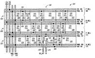
- FIG. 1is a partial top view of an integrated circuit according to the present invention.
- Integrated circuit 101includes logic circuitry implemented in standard cells (e.g. 111 ) in a sea of gates 102 of integrated circuit 101 .
- Sea of gates 102includes a plurality of rows of cells with row of cells 103 , 105 , and 107 being shown in FIG. 1 .
- Row of cells 103includes standard cells 109 , 111 , 113 , 115 , and 117 .
- Row of cells 105includes standard cells 119 , 121 , 123 , 125 , 127 , and 129 .
- Row of cells 107includes standard cells 133 , 132 , and 131 .
- Each standard cellincludes a plurality of transistors to implement a logic function of the integrated circuit.
- these transistorsare CMOS transistors.
- sea of gates 102includes switching cells (e.g. 159 ) that allow the P well areas and the N well areas of the sea of gates to each be selectively biased at different voltages from the supply voltages.
- Each row of cellsincludes an N well area and a P well areas for implementing the transistors of the logic circuitry in the cells of that row.
- the N well areas and the P well areasare doped regions of the semiconductor substrate of integrated circuit 101 .
- row of cells 103includes P well area 169 which runs along the top portion of row of cells 103 , relative to the view shown in FIG. 1 , and a portion of N well area 171 which runs along the bottom of row of cells 103 , relative to the view shown in FIG. 1.
- a portion of N well area 171serves as the N well area for row of cells 105 .
- Each row of cellsincludes multiple tie cells (e.g. 141 ) for coupling a well area to a well bias line (e.g. 181 and 183 ) located in a metal layer above the substrate.
- row of cells 103includes tie cells 141 , 143 , and 145 .
- Each of tie cells 141 , 143 , and 145include a via-contact structure (e.g. 161 for tie cell 141 ) for coupling P well bias line 181 to P well area 169 and a via-contact structure (e.g. 163 for tie cell 141 ) for coupling N well bias line 183 to N well area 171 .
- Via-contact structure 161includes both a via and a well bias contact for coupling bias line 181 , which in one embodiment is located in the second metal layer, to P well area 169 of the substrate.
- Row of cells 105includes tie cells 147 , 149 , and 151 having via-contact structures for coupling N well bias line 186 to N well area 171 and for coupling P well bias line 185 to P well area 173 .
- Row of cells 107includes tie cells 153 , 155 , and 158 having via-contact structures for coupling P well bias line 187 to P well area 173 and coupling N well bias line 189 to N well area 175 .
- P well areas 169 and 173are biased by the voltage of the P well bias lines 181 , 185 , and 187 .
- N well areas 171 and 175are biased by the voltage of N well bias lines 183 , 186 , and 189 .
- the tie cells in each row of cellsare non uniformly spaced from each other. This non uniformity of spacing of the tie cells is due to their placement in areas of the rows of cells that are not occupied by standard cells. The ability to place the tie cells in a non uniform placement aids in the flexibility of the layout of sea of gates 102 .
- the tie cellsare placed in a row such that they are located no further than a certain distance of each other. In one embodiment, the tie cells are located no further than 186 microns from each other in a cell.
- the P well bias lines 181 , 185 , and 187are coupled together by vertical P well bias line 177 , which is located in a higher metal layer (e.g. metal layer 3 ).
- N well bias lines 183 , 186 , and 189are coupled together by vertical N well bias line 179 , also located in metal layer 3 in one embodiment.
- Vertical bias lines 177 and 179are coupled to a charge pump circuit (e.g. 307 of FIG. 3 ) and can be selectively supplied with voltages VPW and VNW, respectively, that are lower than VSS and higher than VDD, respectively, so as to selectively bias the P well areas and N Well areas at VPW and VNW, respectively.
- VDDis 1.5 V
- VSSis 0V
- VNWis 2.1 volts
- VNWmaybe less than VDD and/or VPW maybe greater than VSS.
- Horizontal VDD supply voltage lines 184 and 195are located in the first metal layer and are coupled together by an upper layer vertical VDD line 176 .
- Horizontal VSS supply voltage lines 180 and 198are located in the first metal layer and are coupled together by an upper layer vertical VSS line 178 . These supply voltage lines supply the cells with supply voltages VDD and VSS.
- Sea of gates 102includes switching cells (e.g. 159 ) for coupling the P well bias lines (e.g. 187 ) to the VSS voltage lines (e.g. 198 ) and for coupling the N well bias lines (e.g. 189 ) to the VDD voltage lines (e.g. 195 ) in response to a state of an enable signal on enable line 174 .
- These switching cellsenable the well areas to be selectively biased, based upon the enable signal, to the supply voltages VDD or VSS or to voltages VNW and VPW.
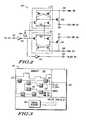
- FIG. 2is a circuit diagram of switching cell 159 .
- Switching cell 159includes a PMOS coupling transistor 203 , which serves as a switch for coupling N well bias line 189 to VDD line 195 through via-contact structures 193 and 194 .
- Via-contact structure 193is also coupled to P well area 173 (see FIG. 1 ).
- Switching cell 159also includes an NMOS coupling transistor 205 for coupling P well bias line 187 to VSS line 198 through via-contact structures 190 and 191 .
- Via-contact structure 190is also coupled to N well area 175 (see FIG. 1 ).
- Switching cell 159receives an enable signal from enable line 174 through via-contact structure 157 .
- the enable signalcontrols whether or not coupling transistors 203 and 205 are conductive to couple line 189 to line 195 and line 187 to line 198 , respectively, to bias N well areas 175 and 171 to VDD and to bias P well areas 173 and 169 to VSS, respectively.
- the signal on enable line 174is high (e.g. VDD)
- transistors 203 and 205are non conductive.
- transistors 203 and 205are conductive.
- Switching cell 159also includes two level shifters 211 and 213 for supplying a voltage to the gates of transistors 203 and 205 , respectively, to maintain the non conductivity of transistors 203 and 205 when the enable signal is in a state (VDD in the embodiment shown) for non conductivity.
- VDDvoltage in the embodiment shown
- the output of inverter 209is also at a high state, which pulls the voltage of the gate of transistor 203 to the voltage level of N well bias line 189 (which is at VNW at that time).
- Providing a switching cell with two coupling transistors responsive to a control linemay enable a switching cell to selectively couple the N well bias line to the VDD line and selectively couple the P well bias line to the VSS line with only one control signal line (e.g. on line 174 ). Accordingly, the number of control signals needed to be routed in the metal layers for selective well biasing may be reduced, thereby saving area in the sea of gates.
- Switching cell 159also includes a control output (e.g. coupled to via-contact structure 156 ) that is coupled to the output enable line (En_Out) 154 for providing the enable signal to a next switching cell (e.g. 312 in FIG. 3 ) of sea of gates 102 whose control input (e.g. the line connected to via-contact structure 157 for switching cell 159 ) is coupled to line 154 .
- a next switching celle.g. 312 in FIG. 3
- control inpute.g. the line connected to via-contact structure 157 for switching cell 159
- invertors 207 and 215 located between via-contact structure 157 and via-contact structure 156provide a delay in the enable signal before being provided to the next sequentially coupled switching cell (e.g. 312 ) located in sea of gates 102 .
- One advantage that may occur from providing a delay in the enable signalis that it may allow each switching cell to bias the N well areas and P well areas with the VDD supply voltage and VSS supply voltage, respectively, at staggered times. Such staggering may limit the in rush current due to the change in voltage of the N well areas and P well areas in that all of the switching cells of a sea of gates do not couple the N well areas to VDD and P well areas to VSS at the same time.
- FIG. 3is a block diagram of integrated circuit 101 .
- integrated circuit 101is an application processor.
- Integrated circuit 101includes a memory 303 , which in one embodiment, is located in an area of integrated circuit 101 that does not include circuitry for selectively biasing its N well areas and P well areas.
- sea of gates 102includes two sets of sequentially coupled switching cells.
- the first setincludes switching cells 159 , 312 , 313 and 314
- the second setincludes switching cells 315 , 316 , 317 , and 318 .
- Each of these switching cellsis similar to switching cell 159 as shown in FIG. 2 .
- Each setis sequentially coupled in that the control output (e.g. the line connected to via-contact structure 156 for switching cell 159 ) for a preceding switching cell in the sequence (e.g. switching cell 159 ) is coupled to the control input (e.g. the line connected to via-contact structure 157 in switching cell 159 ) of the next switching cell in the sequence.
- switching cell 312is the next switching cell in the sequence after switching cell 159 .
- signal line 154is coupled to the control input of switching cell 312 .
- Each switching cell in sea of gates 102is located at a different area of sea of gates 102 .
- Each switching cellcan effectively couple the voltage supply lines carrying VDD and VSS to the N well areas and P well areas, respectively, for a given area.
- the switching cellsare spaced such that all of the sea of gates 102 is covered by an effective area of a switching cell.
- the switching cellsare placed in a non uniform pattern. The ability to place the switching cells in a non uniform pattern may allow for greater flexibility in the design of integrated circuit 101 .
- the effective area of a switching cellis dependent upon the process technology and the size of the coupling transistors of the switching cell.
- Integrated circuit 101includes a control register 309 whose contents control whether the N well and P well areas of sea of gates 102 are to be biased with the supply voltages VDD and VSS or the well bias voltages VNW and VPW.
- control register 309provides a first output signal CON_EN to control the conductivity of the PMOS and NMOS coupling transistors (e.g. 203 and 205 of switching cell 159 ) of the first set of switching cells ( 159 , 312 , 313 , and 314 ) and provides a second output signal CON_EN_ALT for controlling the conductivity of the PMOS and NMOS coupling transistors of the second set of switching cells ( 315 , 316 , 317 , and 318 ).
- control register 309is a control register of the clock control module (not shown) of integrated circuit 101 .
- the contents of register 309may be set by a processor core (not shown) executing code, either internally or externally stored with respect to integrated circuit 101 , or by firmware.
- control register 309may only provide one signal for controlling the bias voltages of the well areas of sea of gates 102 .
- Integrated circuit 101includes a charge pump circuit 307 that provides an enable signal (ENABLE) to line 174 to control the conductivity of the PMOS and NMOS coupling transistors of the first set of switching cells ( 159 , 312 , 313 , and 314 ) in response to the CON_EN signal received from control register 309 .
- Charge pump circuit 307also provides a second enable signal EN_ALT to enable line 337 for controlling the conductivity of the PMOS and NMOS coupling transistors of the second set of switching cells ( 315 , 316 , 317 , and 318 ) in response to the CON_EN_ALT signal.
- Charge pump circuit 307includes an input for receiving the enable signal (EN_BACK) from the control output (e.g. the line connected to via-contact structure 156 ) of switching cell 314 .
- this signalcan be used to indicate whether a change in state of the enable signal ENABLE has propagated through all of the switching cells of the first set of switching cells.
- charge pump circuit 307may also receive a signal from the control output of switching cell 318 .
- Charge pump circuit 307also includes outputs coupled to P well bias line 333 and N well bias line 335 for selectively providing on those lines the VPW voltage and the VNW voltage, respectively, to bias the P well areas of sea of gates 102 and to bias the N well areas of sea of gates 102 , respectively.
- P well bias line 333is coupled to P well bias line 177 and N well bias line 335 is coupled to N well bias line 179 (see FIG. 1 ).
- FIG. 4is a block diagram of charge pump circuit 307 .
- Charge pump circuit 307includes a controller 413 that receives the CON_EN and CON_EN_ALT signals from control register 309 and receives the EN_BACK signal from switching cell 314 . Controller 413 also provides the ENABLE signal and the EN_ALT signal.
- Charge pump circuit 307includes an N well charge pump 403 , that when activated, provides at its output the VNW voltage on line 335 .
- Charge pump circuit 307also includes a P well charge pump 405 , that when activated, provides at its output the VPW voltage on line 333 . When charge pumps 403 and 405 are not activated, their outputs are tri-stated.
- Charge pump circuit 307includes an oscillator 407 , that when turned on, activates charge pumps 403 and 405 .
- Oscillator 407is turned on through OR gate 415 by either N well regulator 411 or P well regulator 409 .
- Regulator 411when turned on by controller 413 , turns on oscillator 407 in response to the voltage of the output of charge pump 403 falling below a predetermined voltage level.
- Regulator 409when turned on by controller 413 , turns on oscillator 407 in response to the voltage of the output of charge pump 405 rising above a predetermined voltage level.
- regulator circuitshaving other configurations may be used.
- the processor core (not shown) of integrated circuit 101initiates the placement of sea of gates 102 in a standby mode where the N well areas are biased at VNW and the P well areas are biased at VPW.
- This initiationis accomplished by writing a value to control register 309 to place the CON_EN signal in a state to make non conductive the PMOS and NMOS coupling transistors of the first set of switching cells ( 159 , 312 , 313 , and 314 ) and to place the CON_EN_ALT signal in a state to make non conductive the PMOS and NMOS coupling transistors of the second set of switching cells ( 315 , 316 , 317 , and 318 ).
- Controller 413places the ENABLE signal in a state to sequentially make the PMOS and NMOS coupling transistors of the first set of switching cells ( 159 , 312 , 313 , and 314 ) non conductive and places the EN_ALT signal in a state to sequentially make the PMOS and NMOS coupling transistors of the second set of switching cells ( 315 , 316 , 317 , and 318 ) non conductive.
- Making the PMOS and NMOS coupling transistors of the switching cells of sea of gates 102 non conductivedecouples the P well bit lines of sea of gates 102 from VSS and decouples the N well bit lines of sea of gates 102 from VDD.
- the states of the CON_EN signal and the CON_EN_ALT signalsmay be changed at different times during a transition from a normal operating mode to a standby operating mode.
- Controller 413When the EN_Back signal has changed states due the change in state in the ENABLE signal (and thus indicating that the coupling transistors of the first set of switching cells have been made non conductive), Controller 413 then turns on regulators 411 and 409 which turn on oscillator 407 to activate N well charge pump 403 and P well charge pump 405 to provide the voltage VNW on line 335 and VPW on line 333 , respectively.
- Providing VNW on line 335 and VPW on line 333 with the coupling transistors of the switching cells being nonconductivebiases the N well areas of sea of gates 102 at VNW and biases the P well areas of sea of gates 102 at VPW respectively.
- control register 309changes the state of the CON_EN signal.
- controller 413disables regulators 411 and 409 such that they turn off oscillator 407 . With oscillator 407 off, the outputs of pumps 403 and 405 (coupled to lines 335 and 333 , respectively) become tri-stated. Controller 413 then changes the state of the ENABLE signal to a state to begin sequentially making the coupling transistors of the first set of switching cells conductive to couple the N well bias lines (e.g.
- control register 309changes the state of the CON_EN_ALT signal.
- controller 413changes the state of the EN_ALT signal to a state to begin sequentially making the coupling transistors of the second set of switching cells conductive to couple the N well bias lines to the VDD voltage supply lines and the P well bias lines to the VSS voltage supply lines.
- Sequentially making conductive the coupling transistors of the switching cellsmay reduce the inrush current from coupling the bias well areas to the voltage supply lines.
- Providing two sets of independently controlled switching cellsmay enable the processor core (not shown) to have some control over the inrush current in that it can determine when the coupling transistors of the second set are made conductive.
- the time at which the coupling transistors of the second set are made conductivemay be programmable or may be made in response to a measured parameter (e.g. measured current).
- a sea of gatesmay include only one set of sequentially coupled switching cell or multiple sets of switching coils.
- controller 413may make the coupling of the coupling transistors of the second sot conductive in response to a change in state of the EN_BACK signal due to a change in state of the ENABLE signal.
- FIG. 5is a flow diagram for one embodiment for the design of an integrated circuit according to the present invention. In one embodiment, the flow of FIG. 5 is implemented with computer aided design tools.
- the locationsare established for the rows of cells in a sea of gates on a substrate of an integrated circuit.
- the layoutis set for the horizontal VDD lines, horizontal VSS lines, horizontal P well bias lines, and horizontal N well Bias lines in the first metal layer.
- the locations of the switching cells in the sea of gatesis established. The switching cells are located such that all of the sea of gates is covered by an effective area of a switching cell.
- the standard cells of the logic circuitryare located in the row of cells.
- tie cellsare located within non designated spaces in the row of cells. In one embodiment, the tie cells are to be placed within a certain distance of each other.
- filler cellsare located in the non designated spaces of the rows of cells.
- the locations of the upper level lines including the vertical VDD lines, the vertical VSS lines, the vertical P well bias lines, and the vertical N well bias linesare set.
- the signal and clock lines locationsare set including the ENABLE, EN_ALT and EN_BACK signals.
- an integrated circuit according to the present inventionmaybe designed by other processes.
- the well bias circuitry shown and described hereinmay be utilized to change the bias of the N well areas and P well areas for other operating modes of the integrated circuit.
- the bias of the N well areas and P well areas of a sea of gatesmay be changed to adjust the threshold voltages of the transistors of a sea of gates during a normal operating mode.
- the control inputs of each switching cell in an arrayare coupled together in parallel.
- an integrated circuitincludes a plurality of rows of cells. Each row of cells of the plurality includes a P well area and an N well area.
- the integrated circuitincludes a plurality of P well bias contacts to bias the P well areas, a plurality of N well bias contacts to bias the N well areas, a first plurality of lines to carry a first voltage, a second plurality of lines to carry a second voltage, and a plurality of switching cells.
- Each switching cellis located in a row of cells of the plurality and is coupled to a line of the first plurality of lines, a line of the second plurality of lines, an N well bias contact of the plurality, and a P well bias contact of the plurality.
- Each of the plurality of switching cellsincludes a control input. In response to the control input being at a first state, the switching cell couples the line of the first plurality of lines to the N well bias contact of the plurality and couples the line of the second plurality of lines to the P well bias contact of the plurality.
- an integrated circuitin another aspect of the invention, includes a row of cells including a doped well area, a well bias contact to bias the doped well area, a first line to carry a first voltage, and a switching cell located in the row of cells.
- the switching cellis coupled to the first line and the well bias contact.
- the switching cellincludes a switch, a control input, and a level shifter. A first terminal of the switch is coupled to the first line, and a second terminal of the switch is coupled to the well bias contact.
- the level shifterIn response to the control input being at a first state, the level shifter provides a voltage equal to a voltage of the second terminal to a gate of the switch to make the switch non conductive.
- an integrated circuitin another aspect of the invention, includes a plurality of rows of cells. Each row of the plurality of rows of cells includes a doped well area of a plurality of well doped areas.
- the integrated circuitincludes a plurality of well bias contacts to bias the doped well areas of the plurality, a first plurality of lines to carry a first voltage, and a plurality of switching cells. Each switching cell of the plurality is located in a row of cells of the plurality of rows of cells. Each switching cell is coupled to a line of the first plurality of lines and a well bias contact of the plurality of well bias contacts. Each switching cell includes a control input.
- the switching cellIn response to the control input being at a first state, the switching cell couples the line of the first plurality of lines to the well bias contact of the plurality of well bias contacts.
- a first switching cell of the plurality of switching cellsincludes a control output coupled to a control input of a second switching cell of the plurality of switching cells. The control output of the first switching cell is responsive to the control input of the first switching cell.
- an integrated circuitin another aspect of the invention, includes a row of cells including a P well area and an N well area, a P well bias contact to bias the P well area, an N well bias contact to bias the N well area, a first line to carry a first supply voltage, a second line to carry a second supply voltage, and a switching cell located in the row of cells.
- the switching cellincludes a first switch coupled to the first line and the N well bias contact.
- the switching cellincludes a second switch coupled to the second line and the P well bias contact.
- the switching cellincludes a control input.
- the first switchIn response to the control input being at a first state, the first switch is conductive to couple the first line to the N well bias contact to bias the N well area at the first supply voltage and the second switch is conductive to couple the second line to the P well bias contact to bias the P well area at the second supply voltage.
- the first and second switchesare non conductive to enable the N well area to be biased at a voltage different from the first supply voltage and to enable the P well area to be biased at a voltage different from the second supply voltage.
Landscapes
- Physics & Mathematics (AREA)
- Engineering & Computer Science (AREA)
- Computer Hardware Design (AREA)
- Computing Systems (AREA)
- General Engineering & Computer Science (AREA)
- Mathematical Physics (AREA)
- Semiconductor Integrated Circuits (AREA)
Abstract
Description
Claims (16)
Priority Applications (2)
| Application Number | Priority Date | Filing Date | Title |
|---|---|---|---|
| US10/366,842US6927429B2 (en) | 2003-02-14 | 2003-02-14 | Integrated circuit well bias circuity |
| US11/168,593US7170116B2 (en) | 2003-02-14 | 2005-06-28 | Integrated circuit well bias circuitry |
Applications Claiming Priority (1)
| Application Number | Priority Date | Filing Date | Title |
|---|---|---|---|
| US10/366,842US6927429B2 (en) | 2003-02-14 | 2003-02-14 | Integrated circuit well bias circuity |
Related Child Applications (1)
| Application Number | Title | Priority Date | Filing Date |
|---|---|---|---|
| US11/168,593DivisionUS7170116B2 (en) | 2003-02-14 | 2005-06-28 | Integrated circuit well bias circuitry |
Publications (2)
| Publication Number | Publication Date |
|---|---|
| US20040159858A1 US20040159858A1 (en) | 2004-08-19 |
| US6927429B2true US6927429B2 (en) | 2005-08-09 |
Family
ID=32849822
Family Applications (2)
| Application Number | Title | Priority Date | Filing Date |
|---|---|---|---|
| US10/366,842Expired - LifetimeUS6927429B2 (en) | 2003-02-14 | 2003-02-14 | Integrated circuit well bias circuity |
| US11/168,593Expired - LifetimeUS7170116B2 (en) | 2003-02-14 | 2005-06-28 | Integrated circuit well bias circuitry |
Family Applications After (1)
| Application Number | Title | Priority Date | Filing Date |
|---|---|---|---|
| US11/168,593Expired - LifetimeUS7170116B2 (en) | 2003-02-14 | 2005-06-28 | Integrated circuit well bias circuitry |
Country Status (1)
| Country | Link |
|---|---|
| US (2) | US6927429B2 (en) |
Cited By (3)
| Publication number | Priority date | Publication date | Assignee | Title |
|---|---|---|---|---|
| US20070007551A1 (en)* | 2002-05-09 | 2007-01-11 | Masayuki Ohayashi | Semiconductor integrated circuit |
| US8890602B2 (en) | 2013-01-16 | 2014-11-18 | Freescale Semiconductor, Inc. | Well-biasing circuit for integrated circuit |
| US20190304847A1 (en)* | 2017-12-07 | 2019-10-03 | Micron Technology, Inc. | Apparatuses Having an Interconnect Extending from an Upper Conductive Structure, Through a Hole in Another Conductive Structure, and to an Underlying Structure |
Families Citing this family (8)
| Publication number | Priority date | Publication date | Assignee | Title |
|---|---|---|---|---|
| AUPR143400A0 (en) | 2000-11-13 | 2000-12-07 | Usf Filtration And Separations Group Inc. | Modified membranes |
| US7306093B2 (en)* | 2003-02-14 | 2007-12-11 | Eastman Chemical Company | Packages, packaging systems, methods for packaging and apparatus for packaging |
| US20050131368A2 (en)* | 2003-03-04 | 2005-06-16 | Diaperoos, Llc | Vacuum-packed diaper |
| US7274247B2 (en)* | 2005-04-04 | 2007-09-25 | Freescale Semiconductor, Inc. | System, method and program product for well-bias set point adjustment |
| US8164378B2 (en)* | 2008-05-06 | 2012-04-24 | Freescale Semiconductor, Inc. | Device and technique for transistor well biasing |
| KR101949503B1 (en)* | 2012-04-18 | 2019-02-18 | 에스케이하이닉스 주식회사 | Stack Type Semiconductor Apparatus, Fabrication Method and Test Method Thereof |
| US9955802B2 (en) | 2015-04-08 | 2018-05-01 | Fasteners For Retail, Inc. | Divider with selectively securable track assembly |
| US10050028B2 (en)* | 2016-11-28 | 2018-08-14 | Taiwan Semiconductor Manufacturing Company Limited | Semiconductor device with reduced leakage current |
Citations (14)
| Publication number | Priority date | Publication date | Assignee | Title |
|---|---|---|---|---|
| US5452245A (en)* | 1993-09-07 | 1995-09-19 | Motorola, Inc. | Memory efficient gate array cell |
| US5493135A (en)* | 1993-08-26 | 1996-02-20 | Aspec Technology, Inc. | Symmetrical multi-layer metal logic array with continuous substrate taps and extension portions for increased gate density |
| US5698872A (en)* | 1989-09-13 | 1997-12-16 | Kabushiki Kaisha Toshiba | Semiconductor memory wherein metallic interconnection layer is applied with the same potential as word line and is connected to word line in regions other than memory cells |
| US5867418A (en)* | 1995-05-29 | 1999-02-02 | Mitsubishi Denki Kabushiki Kaisha | Semiconductor memory device and semiconductor device |
| US5977574A (en)* | 1997-03-28 | 1999-11-02 | Lsi Logic Corporation | High density gate array cell architecture with sharing of well taps between cells |
| US6088255A (en)* | 1998-03-20 | 2000-07-11 | Fujitsu Limited | Semiconductor device with prompt timing stabilization |
| US6107869A (en)* | 1997-06-20 | 2000-08-22 | Hitachi, Ltd. | Semiconductor integrated circuit |
| US6218708B1 (en) | 1998-02-25 | 2001-04-17 | Sun Microsystems, Inc. | Back-biased MOS device and method |
| US6462978B2 (en)* | 1997-08-21 | 2002-10-08 | Hitachi, Ltd. | Method of designing semiconductor integrated circuit device and semiconductor integrated circuit device |
| US6504770B2 (en)* | 1997-06-19 | 2003-01-07 | Hitachi, Ltd. | Semiconductor memory |
| US6507052B1 (en)* | 1999-08-23 | 2003-01-14 | Nec Corporation | Semiconductor memory device with improved reference section |
| US6707139B2 (en)* | 1998-08-28 | 2004-03-16 | Hitachi, Ltd. | Semiconductor device with plural unit regions in which one or more MOSFETs are formed |
| US6768144B2 (en)* | 2001-12-31 | 2004-07-27 | Texas Instruments Incorporated | Method and apparatus for reducing leakage current in an SRAM array |
| US6785182B2 (en)* | 2002-02-13 | 2004-08-31 | Seiko Epson Corporation | Nonvolatile semiconductor memory device |
Family Cites Families (9)
| Publication number | Priority date | Publication date | Assignee | Title |
|---|---|---|---|---|
| WO1995017007A1 (en)* | 1993-12-14 | 1995-06-22 | Oki America, Inc. | Efficient routing method and resulting structure for integrated circuits |
| US5698873A (en)* | 1996-03-08 | 1997-12-16 | Lsi Logic Corporation | High density gate array base cell architecture |
| US5780883A (en)* | 1997-02-28 | 1998-07-14 | Translogic Technology, Inc. | Gate array architecture for multiplexer based circuits |
| US6974978B1 (en)* | 1999-03-04 | 2005-12-13 | Intel Corporation | Gate array architecture |
| US6727533B2 (en)* | 2000-11-29 | 2004-04-27 | Fujitsu Limited | Semiconductor apparatus having a large-size bus connection |
| TW503441B (en)* | 2001-01-18 | 2002-09-21 | Chi Mei Electronic Corp | Layout structure of decoder and manufacturing method |
| US6538314B1 (en)* | 2002-03-29 | 2003-03-25 | International Business Machines Corporation | Power grid wiring for semiconductor devices having voltage islands |
| JP2006114668A (en)* | 2004-10-14 | 2006-04-27 | Sony Corp | Semiconductor integrated circuit and manufacturing method thereof |
| US7298665B2 (en)* | 2004-12-30 | 2007-11-20 | Sandisk 3D Llc | Dual-mode decoder circuit, integrated circuit memory array incorporating same, and related methods of operation |
- 2003
- 2003-02-14USUS10/366,842patent/US6927429B2/ennot_activeExpired - Lifetime
- 2005
- 2005-06-28USUS11/168,593patent/US7170116B2/ennot_activeExpired - Lifetime
Patent Citations (14)
| Publication number | Priority date | Publication date | Assignee | Title |
|---|---|---|---|---|
| US5698872A (en)* | 1989-09-13 | 1997-12-16 | Kabushiki Kaisha Toshiba | Semiconductor memory wherein metallic interconnection layer is applied with the same potential as word line and is connected to word line in regions other than memory cells |
| US5493135A (en)* | 1993-08-26 | 1996-02-20 | Aspec Technology, Inc. | Symmetrical multi-layer metal logic array with continuous substrate taps and extension portions for increased gate density |
| US5452245A (en)* | 1993-09-07 | 1995-09-19 | Motorola, Inc. | Memory efficient gate array cell |
| US5867418A (en)* | 1995-05-29 | 1999-02-02 | Mitsubishi Denki Kabushiki Kaisha | Semiconductor memory device and semiconductor device |
| US5977574A (en)* | 1997-03-28 | 1999-11-02 | Lsi Logic Corporation | High density gate array cell architecture with sharing of well taps between cells |
| US6504770B2 (en)* | 1997-06-19 | 2003-01-07 | Hitachi, Ltd. | Semiconductor memory |
| US6107869A (en)* | 1997-06-20 | 2000-08-22 | Hitachi, Ltd. | Semiconductor integrated circuit |
| US6462978B2 (en)* | 1997-08-21 | 2002-10-08 | Hitachi, Ltd. | Method of designing semiconductor integrated circuit device and semiconductor integrated circuit device |
| US6218708B1 (en) | 1998-02-25 | 2001-04-17 | Sun Microsystems, Inc. | Back-biased MOS device and method |
| US6088255A (en)* | 1998-03-20 | 2000-07-11 | Fujitsu Limited | Semiconductor device with prompt timing stabilization |
| US6707139B2 (en)* | 1998-08-28 | 2004-03-16 | Hitachi, Ltd. | Semiconductor device with plural unit regions in which one or more MOSFETs are formed |
| US6507052B1 (en)* | 1999-08-23 | 2003-01-14 | Nec Corporation | Semiconductor memory device with improved reference section |
| US6768144B2 (en)* | 2001-12-31 | 2004-07-27 | Texas Instruments Incorporated | Method and apparatus for reducing leakage current in an SRAM array |
| US6785182B2 (en)* | 2002-02-13 | 2004-08-31 | Seiko Epson Corporation | Nonvolatile semiconductor memory device |
Non-Patent Citations (1)
| Title |
|---|
| Miroyuki Mizuno et al., "An 18-muA Standby Current 1.8-V, 200-MHz Microprocessor with Self-Substrate-Biased Data-Retention Mode," IEEE Journal of Solid-State Circuits, Nov. 1999, vol. 34, No. 11, pp. 1492-1500. |
Cited By (7)
| Publication number | Priority date | Publication date | Assignee | Title |
|---|---|---|---|---|
| US20070007551A1 (en)* | 2002-05-09 | 2007-01-11 | Masayuki Ohayashi | Semiconductor integrated circuit |
| US7365376B2 (en)* | 2002-05-09 | 2008-04-29 | Renesas Technology Corp. | Semiconductor integrated circuit |
| US20080157381A1 (en)* | 2002-05-09 | 2008-07-03 | Masayuki Ohayashi | Semiconductor integrated circuit |
| US7476915B2 (en) | 2002-05-09 | 2009-01-13 | Renesas Technology Corp. | Semiconductor integrated circuit including a first region and a second region |
| US8890602B2 (en) | 2013-01-16 | 2014-11-18 | Freescale Semiconductor, Inc. | Well-biasing circuit for integrated circuit |
| US20190304847A1 (en)* | 2017-12-07 | 2019-10-03 | Micron Technology, Inc. | Apparatuses Having an Interconnect Extending from an Upper Conductive Structure, Through a Hole in Another Conductive Structure, and to an Underlying Structure |
| US11502006B2 (en)* | 2017-12-07 | 2022-11-15 | Micron Technology, Inc. | Apparatuses having an interconnect extending from an upper conductive structure, through a hole in another conductive structure, and to an underlying structure |
Also Published As
| Publication number | Publication date |
|---|---|
| US20040159858A1 (en) | 2004-08-19 |
| US20060001047A1 (en) | 2006-01-05 |
| US7170116B2 (en) | 2007-01-30 |
Similar Documents
| Publication | Publication Date | Title |
|---|---|---|
| US7683667B2 (en) | Level shifter having single voltage source | |
| US7863971B1 (en) | Configurable power controller | |
| US6556071B2 (en) | Semiconductor integrated circuit | |
| KR101229508B1 (en) | Semiconductor Integrated Cirtuit having plularity of Power Domains | |
| US7800400B2 (en) | Configuration random access memory | |
| US7069522B1 (en) | Various methods and apparatuses to preserve a logic state for a volatile latch circuit | |
| US7436206B2 (en) | Semiconductor integrated circuit | |
| US8451050B2 (en) | Information technology equipment | |
| US6927429B2 (en) | Integrated circuit well bias circuity | |
| US8350409B2 (en) | Semiconductor device and information processing apparatus using the same | |
| CA2201853A1 (en) | High voltage level shifter for switching high voltage in non-volatile memory integrated circuits | |
| US8044696B2 (en) | Delay circuit having long delay time and semiconductor device comprising the same | |
| US7576405B2 (en) | Semiconductor integrated circuit for reducing leak current through MOS transistors | |
| US7131074B2 (en) | Nested voltage island architecture | |
| US7394290B2 (en) | Semiconductor integrated circuit | |
| US8791749B2 (en) | Semicondcutor integrated circuit including power generation block and power supply control block | |
| US6838927B2 (en) | Semiconductor integrated circuit with stabilizing capacity | |
| US7629831B1 (en) | Booster circuit with capacitor protection circuitry | |
| US6384632B2 (en) | Buffer circuit | |
| TWI388977B (en) | Microprocessors, intergarated circuits and methods for selectively biasing substrates | |
| KR100857826B1 (en) | Power network circuit using zigzag power gating and semiconductor device including the same | |
| KR101094918B1 (en) | Phase change memory device with global bit line and its driving method | |
| US8704410B2 (en) | Semiconductor device | |
| US20050097496A1 (en) | High-speed and low-power logical unit | |
| US7418605B1 (en) | System for controlling power to sequential and combinatorial logic circuitry in an integrated circuit |
Legal Events
| Date | Code | Title | Description |
|---|---|---|---|
| AS | Assignment | Owner name:MOTOROLA, INC., ILLINOIS Free format text:ASSIGNMENT OF ASSIGNORS INTEREST;ASSIGNORS:CHUN, CHRISTOPHER K.Y.;SHEU, DER YI;REEL/FRAME:013779/0837 Effective date:20030214 | |
| AS | Assignment | Owner name:FREESCALE SEMICONDUCTOR, INC., TEXAS Free format text:ASSIGNMENT OF ASSIGNORS INTEREST;ASSIGNOR:MOTOROLA, INC;REEL/FRAME:015360/0718 Effective date:20040404 Owner name:FREESCALE SEMICONDUCTOR, INC.,TEXAS Free format text:ASSIGNMENT OF ASSIGNORS INTEREST;ASSIGNOR:MOTOROLA, INC;REEL/FRAME:015360/0718 Effective date:20040404 | |
| STCF | Information on status: patent grant | Free format text:PATENTED CASE | |
| AS | Assignment | Owner name:CITIBANK, N.A. AS COLLATERAL AGENT, NEW YORK Free format text:SECURITY AGREEMENT;ASSIGNORS:FREESCALE SEMICONDUCTOR, INC.;FREESCALE ACQUISITION CORPORATION;FREESCALE ACQUISITION HOLDINGS CORP.;AND OTHERS;REEL/FRAME:018855/0129 Effective date:20061201 Owner name:CITIBANK, N.A. AS COLLATERAL AGENT,NEW YORK Free format text:SECURITY AGREEMENT;ASSIGNORS:FREESCALE SEMICONDUCTOR, INC.;FREESCALE ACQUISITION CORPORATION;FREESCALE ACQUISITION HOLDINGS CORP.;AND OTHERS;REEL/FRAME:018855/0129 Effective date:20061201 | |
| FPAY | Fee payment | Year of fee payment:4 | |
| AS | Assignment | Owner name:CITIBANK, N.A., AS COLLATERAL AGENT,NEW YORK Free format text:SECURITY AGREEMENT;ASSIGNOR:FREESCALE SEMICONDUCTOR, INC.;REEL/FRAME:024397/0001 Effective date:20100413 Owner name:CITIBANK, N.A., AS COLLATERAL AGENT, NEW YORK Free format text:SECURITY AGREEMENT;ASSIGNOR:FREESCALE SEMICONDUCTOR, INC.;REEL/FRAME:024397/0001 Effective date:20100413 | |
| FPAY | Fee payment | Year of fee payment:8 | |
| AS | Assignment | Owner name:CITIBANK, N.A., AS NOTES COLLATERAL AGENT, NEW YORK Free format text:SECURITY AGREEMENT;ASSIGNOR:FREESCALE SEMICONDUCTOR, INC.;REEL/FRAME:030633/0424 Effective date:20130521 Owner name:CITIBANK, N.A., AS NOTES COLLATERAL AGENT, NEW YOR Free format text:SECURITY AGREEMENT;ASSIGNOR:FREESCALE SEMICONDUCTOR, INC.;REEL/FRAME:030633/0424 Effective date:20130521 | |
| AS | Assignment | Owner name:CITIBANK, N.A., AS NOTES COLLATERAL AGENT, NEW YORK Free format text:SECURITY AGREEMENT;ASSIGNOR:FREESCALE SEMICONDUCTOR, INC.;REEL/FRAME:031591/0266 Effective date:20131101 Owner name:CITIBANK, N.A., AS NOTES COLLATERAL AGENT, NEW YOR Free format text:SECURITY AGREEMENT;ASSIGNOR:FREESCALE SEMICONDUCTOR, INC.;REEL/FRAME:031591/0266 Effective date:20131101 | |
| AS | Assignment | Owner name:FREESCALE SEMICONDUCTOR, INC., TEXAS Free format text:PATENT RELEASE;ASSIGNOR:CITIBANK, N.A., AS COLLATERAL AGENT;REEL/FRAME:037356/0553 Effective date:20151207 Owner name:FREESCALE SEMICONDUCTOR, INC., TEXAS Free format text:PATENT RELEASE;ASSIGNOR:CITIBANK, N.A., AS COLLATERAL AGENT;REEL/FRAME:037356/0143 Effective date:20151207 Owner name:FREESCALE SEMICONDUCTOR, INC., TEXAS Free format text:PATENT RELEASE;ASSIGNOR:CITIBANK, N.A., AS COLLATERAL AGENT;REEL/FRAME:037354/0225 Effective date:20151207 | |
| AS | Assignment | Owner name:MORGAN STANLEY SENIOR FUNDING, INC., MARYLAND Free format text:ASSIGNMENT AND ASSUMPTION OF SECURITY INTEREST IN PATENTS;ASSIGNOR:CITIBANK, N.A.;REEL/FRAME:037486/0517 Effective date:20151207 | |
| AS | Assignment | Owner name:MORGAN STANLEY SENIOR FUNDING, INC., MARYLAND Free format text:ASSIGNMENT AND ASSUMPTION OF SECURITY INTEREST IN PATENTS;ASSIGNOR:CITIBANK, N.A.;REEL/FRAME:037518/0292 Effective date:20151207 | |
| AS | Assignment | Owner name:MORGAN STANLEY SENIOR FUNDING, INC., MARYLAND Free format text:SUPPLEMENT TO THE SECURITY AGREEMENT;ASSIGNOR:FREESCALE SEMICONDUCTOR, INC.;REEL/FRAME:039138/0001 Effective date:20160525 | |
| AS | Assignment | Owner name:NXP, B.V., F/K/A FREESCALE SEMICONDUCTOR, INC., NETHERLANDS Free format text:RELEASE BY SECURED PARTY;ASSIGNOR:MORGAN STANLEY SENIOR FUNDING, INC.;REEL/FRAME:040925/0001 Effective date:20160912 Owner name:NXP, B.V., F/K/A FREESCALE SEMICONDUCTOR, INC., NE Free format text:RELEASE BY SECURED PARTY;ASSIGNOR:MORGAN STANLEY SENIOR FUNDING, INC.;REEL/FRAME:040925/0001 Effective date:20160912 | |
| AS | Assignment | Owner name:NXP B.V., NETHERLANDS Free format text:RELEASE BY SECURED PARTY;ASSIGNOR:MORGAN STANLEY SENIOR FUNDING, INC.;REEL/FRAME:040928/0001 Effective date:20160622 | |
| AS | Assignment | Owner name:NXP USA, INC., TEXAS Free format text:CHANGE OF NAME;ASSIGNOR:FREESCALE SEMICONDUCTOR INC.;REEL/FRAME:040652/0180 Effective date:20161107 | |
| FPAY | Fee payment | Year of fee payment:12 | |
| AS | Assignment | Owner name:NXP USA, INC., TEXAS Free format text:CORRECTIVE ASSIGNMENT TO CORRECT THE NATURE OF CONVEYANCE LISTED CHANGE OF NAME SHOULD BE MERGER AND CHANGE PREVIOUSLY RECORDED AT REEL: 040652 FRAME: 0180. ASSIGNOR(S) HEREBY CONFIRMS THE MERGER AND CHANGE OF NAME;ASSIGNOR:FREESCALE SEMICONDUCTOR INC.;REEL/FRAME:041354/0148 Effective date:20161107 | |
| AS | Assignment | Owner name:MORGAN STANLEY SENIOR FUNDING, INC., MARYLAND Free format text:CORRECTIVE ASSIGNMENT TO CORRECT THE REMOVE PATENTS 8108266 AND 8062324 AND REPLACE THEM WITH 6108266 AND 8060324 PREVIOUSLY RECORDED ON REEL 037518 FRAME 0292. ASSIGNOR(S) HEREBY CONFIRMS THE ASSIGNMENT AND ASSUMPTION OF SECURITY INTEREST IN PATENTS;ASSIGNOR:CITIBANK, N.A.;REEL/FRAME:041703/0536 Effective date:20151207 | |
| AS | Assignment | Owner name:SHENZHEN XINGUODU TECHNOLOGY CO., LTD., CHINA Free format text:CORRECTIVE ASSIGNMENT TO CORRECT THE TO CORRECT THE APPLICATION NO. FROM 13,883,290 TO 13,833,290 PREVIOUSLY RECORDED ON REEL 041703 FRAME 0536. ASSIGNOR(S) HEREBY CONFIRMS THE THE ASSIGNMENT AND ASSUMPTION OF SECURITYINTEREST IN PATENTS.;ASSIGNOR:MORGAN STANLEY SENIOR FUNDING, INC.;REEL/FRAME:048734/0001 Effective date:20190217 | |
| AS | Assignment | Owner name:NXP B.V., NETHERLANDS Free format text:RELEASE BY SECURED PARTY;ASSIGNOR:MORGAN STANLEY SENIOR FUNDING, INC.;REEL/FRAME:050744/0097 Effective date:20190903 | |
| AS | Assignment | Owner name:MORGAN STANLEY SENIOR FUNDING, INC., MARYLAND Free format text:CORRECTIVE ASSIGNMENT TO CORRECT THE REMOVE APPLICATION11759915 AND REPLACE IT WITH APPLICATION 11759935 PREVIOUSLY RECORDED ON REEL 037486 FRAME 0517. ASSIGNOR(S) HEREBY CONFIRMS THE ASSIGNMENT AND ASSUMPTION OF SECURITYINTEREST IN PATENTS;ASSIGNOR:CITIBANK, N.A.;REEL/FRAME:053547/0421 Effective date:20151207 | |
| AS | Assignment | Owner name:NXP B.V., NETHERLANDS Free format text:CORRECTIVE ASSIGNMENT TO CORRECT THE REMOVEAPPLICATION 11759915 AND REPLACE IT WITH APPLICATION11759935 PREVIOUSLY RECORDED ON REEL 040928 FRAME 0001. ASSIGNOR(S) HEREBY CONFIRMS THE RELEASE OF SECURITYINTEREST;ASSIGNOR:MORGAN STANLEY SENIOR FUNDING, INC.;REEL/FRAME:052915/0001 Effective date:20160622 | |
| AS | Assignment | Owner name:NXP, B.V. F/K/A FREESCALE SEMICONDUCTOR, INC., NETHERLANDS Free format text:CORRECTIVE ASSIGNMENT TO CORRECT THE REMOVEAPPLICATION 11759915 AND REPLACE IT WITH APPLICATION11759935 PREVIOUSLY RECORDED ON REEL 040925 FRAME 0001. ASSIGNOR(S) HEREBY CONFIRMS THE RELEASE OF SECURITYINTEREST;ASSIGNOR:MORGAN STANLEY SENIOR FUNDING, INC.;REEL/FRAME:052917/0001 Effective date:20160912 |