US6927413B2 - Semiconductor device including band-engineered superlattice - Google Patents
Semiconductor device including band-engineered superlatticeDownload PDFInfo
- Publication number
- US6927413B2 US6927413B2US10/717,375US71737503AUS6927413B2US 6927413 B2US6927413 B2US 6927413B2US 71737503 AUS71737503 AUS 71737503AUS 6927413 B2US6927413 B2US 6927413B2
- Authority
- US
- United States
- Prior art keywords
- superlattice
- semiconductor device
- semiconductor
- layers
- group
- Prior art date
- Legal status (The legal status is an assumption and is not a legal conclusion. Google has not performed a legal analysis and makes no representation as to the accuracy of the status listed.)
- Expired - Lifetime, expires
Links
Images


Classifications
- H—ELECTRICITY
- H10—SEMICONDUCTOR DEVICES; ELECTRIC SOLID-STATE DEVICES NOT OTHERWISE PROVIDED FOR
- H10D—INORGANIC ELECTRIC SEMICONDUCTOR DEVICES
- H10D62/00—Semiconductor bodies, or regions thereof, of devices having potential barriers
- H10D62/80—Semiconductor bodies, or regions thereof, of devices having potential barriers characterised by the materials
- H10D62/81—Semiconductor bodies, or regions thereof, of devices having potential barriers characterised by the materials of structures exhibiting quantum-confinement effects, e.g. single quantum wells; of structures having periodic or quasi-periodic potential variation
- H10D62/815—Semiconductor bodies, or regions thereof, of devices having potential barriers characterised by the materials of structures exhibiting quantum-confinement effects, e.g. single quantum wells; of structures having periodic or quasi-periodic potential variation of structures having periodic or quasi-periodic potential variation, e.g. superlattices or multiple quantum wells [MQW]
- H10D62/8161—Semiconductor bodies, or regions thereof, of devices having potential barriers characterised by the materials of structures exhibiting quantum-confinement effects, e.g. single quantum wells; of structures having periodic or quasi-periodic potential variation of structures having periodic or quasi-periodic potential variation, e.g. superlattices or multiple quantum wells [MQW] potential variation due to variations in composition or crystallinity, e.g. heterojunction superlattices
- H10D62/8162—Semiconductor bodies, or regions thereof, of devices having potential barriers characterised by the materials of structures exhibiting quantum-confinement effects, e.g. single quantum wells; of structures having periodic or quasi-periodic potential variation of structures having periodic or quasi-periodic potential variation, e.g. superlattices or multiple quantum wells [MQW] potential variation due to variations in composition or crystallinity, e.g. heterojunction superlattices having quantum effects only in the vertical direction, i.e. layered structures having quantum effects solely resulting from vertical potential variation
- B—PERFORMING OPERATIONS; TRANSPORTING
- B82—NANOTECHNOLOGY
- B82Y—SPECIFIC USES OR APPLICATIONS OF NANOSTRUCTURES; MEASUREMENT OR ANALYSIS OF NANOSTRUCTURES; MANUFACTURE OR TREATMENT OF NANOSTRUCTURES
- B82Y10/00—Nanotechnology for information processing, storage or transmission, e.g. quantum computing or single electron logic
- H—ELECTRICITY
- H10—SEMICONDUCTOR DEVICES; ELECTRIC SOLID-STATE DEVICES NOT OTHERWISE PROVIDED FOR
- H10D—INORGANIC ELECTRIC SEMICONDUCTOR DEVICES
- H10D30/00—Field-effect transistors [FET]
- H10D30/60—Insulated-gate field-effect transistors [IGFET]
- H10D30/601—Insulated-gate field-effect transistors [IGFET] having lightly-doped drain or source extensions, e.g. LDD IGFETs or DDD IGFETs
- H—ELECTRICITY
- H10—SEMICONDUCTOR DEVICES; ELECTRIC SOLID-STATE DEVICES NOT OTHERWISE PROVIDED FOR
- H10D—INORGANIC ELECTRIC SEMICONDUCTOR DEVICES
- H10D30/00—Field-effect transistors [FET]
- H10D30/60—Insulated-gate field-effect transistors [IGFET]
- H10D30/751—Insulated-gate field-effect transistors [IGFET] having composition variations in the channel regions
- H—ELECTRICITY
- H10—SEMICONDUCTOR DEVICES; ELECTRIC SOLID-STATE DEVICES NOT OTHERWISE PROVIDED FOR
- H10D—INORGANIC ELECTRIC SEMICONDUCTOR DEVICES
- H10D62/00—Semiconductor bodies, or regions thereof, of devices having potential barriers
- H10D62/80—Semiconductor bodies, or regions thereof, of devices having potential barriers characterised by the materials
- H10D62/81—Semiconductor bodies, or regions thereof, of devices having potential barriers characterised by the materials of structures exhibiting quantum-confinement effects, e.g. single quantum wells; of structures having periodic or quasi-periodic potential variation
- H10D62/815—Semiconductor bodies, or regions thereof, of devices having potential barriers characterised by the materials of structures exhibiting quantum-confinement effects, e.g. single quantum wells; of structures having periodic or quasi-periodic potential variation of structures having periodic or quasi-periodic potential variation, e.g. superlattices or multiple quantum wells [MQW]
- H10D62/8161—Semiconductor bodies, or regions thereof, of devices having potential barriers characterised by the materials of structures exhibiting quantum-confinement effects, e.g. single quantum wells; of structures having periodic or quasi-periodic potential variation of structures having periodic or quasi-periodic potential variation, e.g. superlattices or multiple quantum wells [MQW] potential variation due to variations in composition or crystallinity, e.g. heterojunction superlattices
- H10D62/8162—Semiconductor bodies, or regions thereof, of devices having potential barriers characterised by the materials of structures exhibiting quantum-confinement effects, e.g. single quantum wells; of structures having periodic or quasi-periodic potential variation of structures having periodic or quasi-periodic potential variation, e.g. superlattices or multiple quantum wells [MQW] potential variation due to variations in composition or crystallinity, e.g. heterojunction superlattices having quantum effects only in the vertical direction, i.e. layered structures having quantum effects solely resulting from vertical potential variation
- H10D62/8164—Semiconductor bodies, or regions thereof, of devices having potential barriers characterised by the materials of structures exhibiting quantum-confinement effects, e.g. single quantum wells; of structures having periodic or quasi-periodic potential variation of structures having periodic or quasi-periodic potential variation, e.g. superlattices or multiple quantum wells [MQW] potential variation due to variations in composition or crystallinity, e.g. heterojunction superlattices having quantum effects only in the vertical direction, i.e. layered structures having quantum effects solely resulting from vertical potential variation comprising only semiconductor materials
- H—ELECTRICITY
- H10—SEMICONDUCTOR DEVICES; ELECTRIC SOLID-STATE DEVICES NOT OTHERWISE PROVIDED FOR
- H10D—INORGANIC ELECTRIC SEMICONDUCTOR DEVICES
- H10D84/00—Integrated devices formed in or on semiconductor substrates that comprise only semiconducting layers, e.g. on Si wafers or on GaAs-on-Si wafers
- H10D84/01—Manufacture or treatment
- H10D84/0123—Integrating together multiple components covered by H10D12/00 or H10D30/00, e.g. integrating multiple IGBTs
- H10D84/0126—Integrating together multiple components covered by H10D12/00 or H10D30/00, e.g. integrating multiple IGBTs the components including insulated gates, e.g. IGFETs
- H10D84/0165—Integrating together multiple components covered by H10D12/00 or H10D30/00, e.g. integrating multiple IGBTs the components including insulated gates, e.g. IGFETs the components including complementary IGFETs, e.g. CMOS devices
- H10D84/0167—Manufacturing their channels
- H—ELECTRICITY
- H10—SEMICONDUCTOR DEVICES; ELECTRIC SOLID-STATE DEVICES NOT OTHERWISE PROVIDED FOR
- H10D—INORGANIC ELECTRIC SEMICONDUCTOR DEVICES
- H10D84/00—Integrated devices formed in or on semiconductor substrates that comprise only semiconducting layers, e.g. on Si wafers or on GaAs-on-Si wafers
- H10D84/01—Manufacture or treatment
- H10D84/02—Manufacture or treatment characterised by using material-based technologies
- H10D84/03—Manufacture or treatment characterised by using material-based technologies using Group IV technology, e.g. silicon technology or silicon-carbide [SiC] technology
- H10D84/038—Manufacture or treatment characterised by using material-based technologies using Group IV technology, e.g. silicon technology or silicon-carbide [SiC] technology using silicon technology, e.g. SiGe
Definitions
- the present inventionrelates to the field of semiconductors, and, more particularly, to semiconductors having enhanced properties based upon energy band engineering and associated methods.
- U.S. Pat. No. 6,472,685 B2 to Takagidiscloses a semiconductor device including a silicon and carbon layer sandwiched between silicon layers so that the conduction band and valence band of the second silicon layer receive a tensile strain. Electrons having a smaller effective mass, and which have been induced by an electric field applied to the gate electrode, are confined in the second silicon layer, thus, an n-channel MOSFET is asserted to have a higher mobility.
- U.S. Pat. No. 4,937,204 to Ishibashi et al.discloses a superlattice in which a plurality of layers, less than eight monolayers, and containing a fraction or a binary compound semiconductor layers, are alternately and epitaxially grown. The direction of main current flow is perpendicular to the layers of the superlattice.
- U.S. Pat. No. 5,357,119 to Wang et al.discloses a Si—Ge short period superlattice with higher mobility achieved by reducing alloy scattering in the superlattice.
- U.S. Pat. No. 5,683,934 to Candelariadiscloses an enhanced mobility MOSFET including a channel layer comprising an alloy of silicon and a second material substitutionally present in the silicon lattice at a percentage that places the channel layer under tensile stress.
- U.S. Pat. No. 5,216,262 to Tsudiscloses a quantum well structure comprising two barrier regions and a thin epitaxially grown semiconductor layer sandwiched between the barriers.
- Each barrier regionconsists of alternate layers of SiO 2 /Si with a thickness generally in a range of two to six monolayers. A much thicker section of silicon is sandwiched between the barriers.
- An article entitled “Phenomena in silicon nanostructure devices” also to Tsu and published online Sep. 6, 2000 by Applied Physics and Materials Science & Processing, pp. 391-402discloses a semiconductor-atomic superlattice (SAS) of silicon and oxygen.
- the Si/O superlatticeis disclosed as useful in a silicon quantum and light-emitting devices.
- a green electromuminescence diode structurewas constructed and tested. Current flow in the diode structure is vertical, that is, perpendicular to the layers of the SAS.
- the disclosed SASmay include semiconductor layers separated by adsorbed species such as oxygen atoms, and CO molecules. The silicon growth beyond the adsorbed monolayer of oxygen is described as epitaxial with a fairly low defect density.
- One SAS structureincluded a 1.1 nm thick silicon portion that is about eight atomic layers of silicon, and another structure had twice this thickness of silicon.
- An article to Luo et al. entitled “Chemical Design of Direct-Gap Light-Emitting Silicon” published in Physical Review Letters, Vol. 89, No. 7 (Aug. 12, 2002)further discusses the light emitting SAS structures of Tsu.
- APBGAperiodic Photonic Band-Gap
- material parametersfor example, the location of band minima, effective mass, etc, can be tailored to yield new aperiodic materials with desirable band-structure characteristics.
- Other parameterssuch as electrical conductivity, thermal conductivity and dielectric permittivity or magnetic permeability are disclosed as also possible to be designed into the material.
- a semiconductor devicecomprising a superlattice including a plurality of stacked groups of layers. More particularly, the device may also include regions for causing transport of charge carriers through the superlattice in a parallel direction relative to the stacked groups of layers.
- Each group of layers of the superlatticemay comprise a plurality of stacked base semiconductor monolayers defining a base semiconductor portion, and an energy band-modifying layer thereon.
- the energy-band modifying layermay comprise at least one non-semiconductor monolayer constrained within a crystal lattice of adjacent base semiconductor portions so that the superlattice has a higher charge carrier mobility than would otherwise be present.
- the superlatticemay also have a common energy band structure therein.
- each base semiconductor portionmay comprise silicon, and each energy band-modifying layer may comprise oxygen.
- Each energy band-modifying layermay be a single monolayer thick, and each base semiconductor portion may be less than eight monolayers thick, such as two to six monolayers thick, for example, in some embodiments.
- the superlatticemay further have a substantially direct energy bandgap, as may especially advantageous for opto-electronic devices.
- the superlatticemay further comprise a base semiconductor cap layer on an uppermost group of layers.
- all of the base semiconductor portionsmay be a same number of monolayers thick. In other embodiments, at least some of the base semiconductor portions may be a different number of monolayers thick. In still other embodiments, all of the base semiconductor portions may be a different number of monolayers thick.
- Each non-semiconductor monolayeris desirably thermally stable through deposition of a next layer to thereby facilitate manufacturing.
- Each base semiconductor portionmay comprise a base semiconductor selected from the group consisting of Group IV semiconductors, Group III-V semiconductors, and Group II-VI semiconductors.
- each energy band-modifying layermay comprise a non-semiconductor selected from the group consisting of oxygen, nitrogen, fluorine, and carbon-oxygen.
- the higher mobilitymay result from a lower conductivity effective mass.
- This lower conductivity effective massmay be less than two-thirds the conductivity effective mass than would otherwise occur.
- the superlatticemay further comprise at least one type of conductivity dopant therein.
- FIG. 1is a schematic cross-sectional view of a semiconductor device in accordance with the present invention.
- FIG. 2is a greatly enlarged schematic cross-sectional view of the superlattice as shown in FIG. 1 .
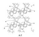
- FIG. 3is a perspective schematic atomic diagram of a portion of the superlattice shown in FIG. 1 .
- FIG. 4is a greatly enlarged schematic cross-sectional view of another embodiment of a superlattice that may be used in the device of FIG. 1 .
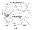
- FIG. 5Ais a graph of the calculated band structure from the gamma point (G) for both bulk silicon as in the prior art, and for the 4/1 Si/O superlattice as shown in FIGS. 1-3 .
- FIG. 5Bis a graph of the calculated band structure from the Z point for both bulk silicon as in the prior art, and for the 4/1 Si/O superlattice as shown in FIGS. 1-3 .
- FIG. 5Cis a graph of the calculated band structure from both the gamma and Z points for both bulk silicon as in the prior art, and for the 5/1/3/1 Si/O superlattice as shown in FIG. 4 .
- FIGS. 6A-6Hare schematic cross-sectional views of a portion of another semiconductor device in accordance with the present invention during the making thereof.
- the present inventionrelates to controlling the properties of semiconductor materials at the atomic or molecular level to achieve improved performance within semiconductor devices. Further, the invention relates to the identification, creation, and use of improved materials for use in the conduction paths of semiconductor devices.
- the conductivity reciprocal effective mass tensoris such that a tensorial component of the conductivity of the material is greater for greater values of the corresponding component of the conductivity reciprocal effective mass tensor.
- the superlattices described hereinset the values of the conductivity reciprocal effective mass tensor so as to enhance the conductive properties of the material, such as typically for a preferred direction of charge carrier transport.
- the inverse of the appropriate tensor elementis referred to as the conductivity effective mass.
- the conductivity effective mass for electrons/holes as described above and calculated in the direction of intended carrier transportis used to distinguish improved materials.
- One such examplewould be a superlattice 25 material for a channel region in a CMOS device.
- a planar MOSFET 20 including the superlattice 25 in accordance with the inventionis now first described with reference to FIG. 1 .
- the materials identified hereincould be used in many different types of semiconductor devices, such as discrete devices and/or integrated circuits.
- the illustrated MOSFET 20includes a substrate 21 , source/drain regions 22 , 23 , source/drain extensions 26 , 27 , and a channel region therebetween provided by the superlattice 25 .
- Source/drain silicide layers 30 , 31 and source/drain contacts 32 , 33overlie the source/drain regions as will be appreciated by those skilled in the art.
- Regions indicated by dashed lines 34 , 35are optional vestigial portions formed originally with the superlattice, but thereafter heavily doped. In other embodiments, these vestigial superlattice regions 34 , 35 may not be present as will also be appreciated by those skilled in the art.
- a gate 35illustratively includes a gate insulating layer 37 adjacent the channel provided by the superlattice 25 , and a gate electrode layer 36 on the gate insulating layer. Sidewall spacers 40 , 41 are also provided in the illustrated MOSFET 20 .
- the Applicantshave identified improved materials or structures for the channel region of the MOSFET 20. More specifically, the Applicants have identified materials or structures having energy band structures for which the appropriate conductivity effective masses for electrons and/or holes are substantially less than the corresponding values for silicon.
- the materials or structuresare in the form of a superlattice 25 whose structure is controlled at the atomic or molecular level and may be formed using known techniques of atomic or molecular layer deposition.
- the superlattice 25includes a plurality of layer groups 45 a - 45 n arranged in stacked relation as perhaps best understood with specific reference to the schematic cross-sectional view of FIG. 2 .
- Each group of layers 45 a - 45 n of the superlattice 25illustratively includes a plurality of stacked base.
- semiconductor monolayers 46defining a respective base semiconductor portion 46 a - 46 n and an energy band-modifying layer 50 thereon.
- the energy band-modifying layers 50are indicated by stippling in FIG. 2 for clarity of explanation.
- the energy-band modifying layer 50illustratively comprises one non-semiconductor monolayer constrained within a crystal lattice of adjacent base semiconductor portions. In other embodiments, more than one such monolayer may be possible. Applicants theorize without wishing to be bound thereto that energy band-modifying layers 50 and adjacent base semiconductor portions 46 a - 46 n cause the superlattice 25 to have a lower appropriate conductivity effective mass for the charge carriers in the parallel layer direction than would otherwise be present. Considered another way, this parallel direction is orthogonal to the stacking direction. The band modifying layers 50 may also cause the superlattice 25 to have a common energy band structure.
- the semiconductor devicesuch as the illustrated MOSFET 20
- the superlattice 25may further have a substantially direct energy bandgap that may be particularly advantageous for opto-electronic devices, for example, as described in further detail below.
- the source/drain regions 22 , 23 and gate 35 of the MOSFET 20may be considered as regions for causing the transport of charge carriers through the superlattice in a parallel direction relative to the layers of the stacked groups 45 a - 45 n .
- Other such regionsare also contemplated by the present invention.
- the superlattice 25also illustratively includes a cap layer 52 on an upper layer group 45 n .
- the cap layer 52may comprise a plurality of base semiconductor monolayers 46 .
- the cap layer 52may have between 2 to 100 monolayers of the base semiconductor, and, more preferably between 10 to 50 monolayers.
- Each base semiconductor portion 46 a - 46 nmay comprise a base semiconductor selected from the group consisting of Group IV semiconductors, Group III-V semiconductors, and Group II-VI semiconductors.
- Group IV semiconductorsalso includes Group IV-IV semiconductors as will be appreciated by those skilled in the art.
- Each energy band-modifying layer 50may comprise a non-semiconductor selected from the group consisting of oxygen, nitrogen, fluorine, and carbon-oxygen, for example.
- the non-semiconductoris also desirably thermally stable through deposition of a next layer to thereby facilitate manufacturing.
- the non-semiconductormay be another inorganic or organic element or compound that is compatible with the given semiconductor processing as will be appreciated by those skilled in the art.
- the term monolayeris meant to include a single atomic layer and also a single molecular layer.
- the energy band-modifying layer 50 provided by a single monolayeris also meant to include a monolayer wherein not all of the possible sites are occupied.
- a 4/1 repeating structureis illustrated for silicon as the base semiconductor material, and oxygen as the energy band-modifying material. Only half of the possible sites for oxygen are occupied. In other embodiments and/or with different materials this one half occupation would not necessarily be the case as will be appreciated by those skilled in the art. Indeed it can be seen even in this schematic diagram, that individual atoms of oxygen in a given monolayer are not precisely aligned along a flat plane as will also be appreciated by those of skill in the art of atomic deposition.
- Silicon and oxygenare currently widely used in conventional semiconductor processing, and, hence, manufacturers will be readily able to use these materials as described herein.
- Atomic or monolayer depositionis also now widely used. Accordingly, semiconductor devices incorporating the superlattice 25 in accordance with the invention may be readily adopted and implemented as will be appreciated by those skilled in the art.
- the number of silicon monolayersshould desirably be seven or less so that the energy band of the superlattice is common or relatively uniform throughout to achieve the desired advantages.
- the 4/1 repeating structure shown in FIGS. 2 and 3for Si/O has been modeled to indicate an enhanced mobility for electrons and holes in the X direction.
- the calculated conductivity effective mass for electronsis 0.26 and for the 4/1 SiO superlattice in the X direction it is 0.12 resulting in a ratio of 0.46.
- the calculation for holesyields values of 0.36 for bulk silicon and 0.16 for the 4/1 Si/O superlattice resulting in a ratio of 0.44.
- While such a directionally preferential featuremay be desired in certain semiconductor devices, other devices may benefit from a more uniform increase in mobility in any direction parallel to the groups of layers. It may also be beneficial to have an increased mobility for both electrons or holes, or just one of these types of charge carriers as will be appreciated by those skilled in the art.
- the lower conductivity effective mass for the 4/1 Si/O embodiment of the superlattice 25may be less than two-thirds the conductivity effective mass than would otherwise occur, and this applies for both electrons and holes.
- the superlattice 25may further comprise at least one type of conductivity dopant therein as will also be appreciated by those skilled in the art.
- FIG. 4another embodiment of a superlattice 25 ′ in accordance with the invention having different properties is now described.
- a repeating pattern of 3/1/5/1is illustrated. More particularly, the lowest base semiconductor portion 46 a ′ has three monolayers, and the second lowest base semiconductor portion 46 b ′ has five monolayers. This pattern repeats throughout the superlattice 25 ′
- the energy band-modifying layers 50 ′may each include a single monolayer.
- the enhancement of charge carrier mobilityis independent of orientation in the plane of the layers.
- all of the base semiconductor portions of a superlatticemay be a same number of monolayers thick. In other embodiments, at least some of the base semiconductor portions may be a different number of monolayers thick. In still other embodiments, all of the base semiconductor portions may be a different number of monolayers thick.
- FIGS. 5A-5Cband structures calculated using Density Functional Theory (DFT) are presented. It is well known in the art that DFT underestimates the absolute value of the bandgap. Hence all bands above the gap may be shifted by an appropriate “scissors correction”. However the shape of the band is known to be much more reliable. The vertical energy axes should be interpreted in this light.
- DFTDensity Functional Theory
- FIG. 5Ashows the calculated band structure from the gamma point (G) for both bulk silicon (represented by continuous lines) and for the 4/1 Si/O superlattice 25 as shown in FIGS. 1-3 (represented by dotted lines).
- the directionsrefer to the unit cell of the 4/1 Si/O structure and not to the conventional unit cell of Si, although the (001) direction in the figure does correspond to the (001) direction of the conventional unit cell of Si, and, hence, shows the expected location of the Si conduction band minimum.
- the (100) and (010) directions in the figurecorrespond to the (110) and ( ⁇ 110) directions of the conventional Si unit cell.
- the bands of Si on the figureare folded to represent them on the appropriate reciprocal lattice directions for the 4/1 Si/O structure.
- the conduction band minimum for the 4/1 Si/O structureis located at the gamma point in contrast to bulk silicon (Si), whereas the valence band minimum occurs at the edge of the Brillouin zone in the (001) direction which we refer to as the Z point.
- the greater curvature of the conduction band minimum for the 4/1 Si/O structurecompared to the curvature of the conduction band minimum for Si owing to the band splitting due to the perturbation introduced by the additional oxygen layer.
- FIG. 5Bshows the calculated band structure from the Z point for both bulk silicon (continuous lines) and for the 4/1 Si/O superlattice 25 (dotted lines). This figure illustrates the enhanced curvature of the valence band in the (100) direction.
- FIG. 5Cshows the calculated band structure from the both the gamma and Z point for both bulk silicon (continuous lines) and for the 5/1/3/1 Si/O structure of the superlattice 25 ′ of FIG. 4 (dotted lines). Due to the symmetry of the 5/1/3/1 Si/O structure, the calculated band structures in the (100) and (010) directions are equivalent. Thus the conductivity effective mass and mobility are expected to be isotropic in the plane parallel to the layers, i.e. perpendicular to the (001) stacking direction. Note that in the 5/1/3/1 Si/O example the conduction band minimum and the valence band maximum are both at or close to the Z point.
- the appropriate comparison and discriminationmay be made via the conductivity reciprocal effective mass tensor calculation. This leads Applicants to further theorize that the 5/1/3/1 superlattice 25 ′ should be substantially direct bandgap. As will be understood by those skilled in the art, the appropriate matrix element for optical transition is another indicator of the distinction between direct and indirect bandgap behavior.
- FIGS. 6A-6Ha discussion is provided of the formation of a channel region provided by the above-described superlattice 25 in a simplified CMOS fabrication process for manufacturing PMOS and NMOS transistors.
- the example processbegins with an eight-inch wafer of lightly doped P-type or N-type single crystal silicon with ⁇ 100> orientation 402 .
- the formation of two transistors, one NMOS and one PMOSwill be shown.
- a deep N-well 404is implanted in the substrate 402 for isolation.
- N-well and P-well regions 406, 408, respectively,are formed using an SiO 2 /Si 3 N 4 mask prepared using known techniques.
- the strip steprefers to removing the mask (in this case, photoresist and silicon nitride).
- the drive-in stepis used to locate the dopants at the appropriate depth, assuming the implantation is lower energy (i.e. 80 keV) rather than higher energy (200-300 keV). A typical drive-in condition would be approximately 9-10 hrs. at 1100-1150° C.
- the drive-in stepalso anneals out implantation damage. If the implant is of sufficient energy to put the ions at the correct depth then an anneal step follows, which is lower temperature and shorter. A clean step comes before an oxidation step so as to avoid contaminating the furnaces with organics, metals, etc. Other known ways or processes for reaching this point may be used as well.
- FIGS. 6C-6Han NMOS device will be shown in one side 200 and a PMOS device will be shown in the other side 400 .
- FIG. 6Cdepicts shallow trench isolation in which the wafer is patterned, the trenches 410 are etched (0.3-0.8 um), a thin oxide is grown, the trenches are filled with SiO 2 , and then the surface is planarized.
- FIG. 6Ddepicts the definition and deposition of the superlattice of the present invention as the channel regions 412 , 414 .
- An Si 2 mask(not shown) is formed, a superlattice of the present invention is deposited using atomic layer deposition, an epitaxial silicon cap layer is formed, and the surface is planarized to arrive at the structure of FIG. 6 D.
- the epitaxial silicon cap layermay have a preferred thickness to prevent superlattice consumption during gate oxide growth, or any other subsequent oxidations, while at the same time reducing or minimizing the thickness of the silicon cap layer to reduce any parallel path of conduction with the superlattice.
- the silicon cap layermay be greater than 45% of the grown gate oxide thickness plus a small incremental amount to account for manufacturing tolerances known to those skilled in the art. For the present example, and assuming growth of a 25 angstrom gate, one may use approximately 13-15 angstroms of silicon cap thickness.
- FIG. 6Edepicts the devices after the gate oxide layers 416 and the gates 418 are formed.
- a thin gate oxideis deposited, and steps of poly deposition, patterning, and etching are performed.
- Poly depositionrefers to low pressure chemical vapor deposition (LPCVD) of silicon onto an oxide (hence it forms a polycrystalline material). The step includes doping with P+ or As ⁇ to make it conducting and the layer is around 250 nm thick.
- the pattern stepis made up of spinning photoresist, baking it, exposing it to light (photolithography step), and developing the resist. Usually, the pattern is then transferred to another layer (oxide or nitride) which acts as an etch mask during the etch step.
- the etch steptypically is a plasma etch (anisotropic, dry etch) that is material selective (e.g. etches silicon 10 times faster than oxide) and transfers the lithography pattern into the material of interest.
- lowly doped source and drain regions 420 , 422are formed adjacent the channels 424 and 426 . These regions are formed using n-type and p-type LDD implantation, annealing, and cleaning. “LDD” refers to n-type lowly doped drain, or on the source side, p-type lowly doped source. This is a low energy/low dose implant that is the same ion type as the source/drain. An anneal step may be used after the LDD implantation, but depending on the specific process, it may be omitted. The clean step is a chemical etch to remove metals and organics prior to depositing an oxide layer.
- FIG. 6Gshows the spacer 428 formation and the source and drain implants.
- An SiO 2 maskis deposited and etched back.
- N-type and p-type ion implantationis used to form the source and drain regions 430 , 432 , 434 , and 436 .
- the structureis annealed and cleaned.
- FIG. 6Hdepicts the self-aligned silicides 438 formation, also known as salicidation.
- the salicidation processincludes metal deposition (e.g. Ti), nitrogen annealing, metal etching, and a second annealing. This, of course, is just one example of a process and device in which the present invention may be used, and those of skill in the art will understand its application and use in many other processes and devices.
- the structures of the present inventionmay be formed on a portion of a wafer or across substantially all of a wafer. In other processes and devices the structures of the present invention may be formed on a portion of a wafer or across substantially all of a wafer.
- selective depositionis not used. Instead, a blanket layer may be formed and a masking step may be used to remove material between devices, such as using the STI areas as an etch stop. This may use a controlled deposition over a patterned oxide/Si wafer.
- the use of an atomic layer deposition toolmay also not be needed in some embodiments.
- the monolayersmay be formed using a CVD tool with process conditions compatible with control of monolayers as will be appreciated by those skilled in the art. Although planarization is discussed above, it may not be needed in some process embodiments.
- the superlattice structuremay also formed prior to formation of the STI regions to thereby eliminate a masking step. Moreover, in yet other variations, the superlattice structure could be formed prior to formation of the wells, for example.
- the method in accordance with the present inventionmay include forming a superlattice 25 including a plurality of stacked groups of layers 45 a - 45 n .
- the methodmay also include forming regions for causing transport of charge carriers through the superlattice in a parallel direction relative to the stacked groups of layers.
- Each group of layers of the superlatticemay comprise a plurality of stacked base semiconductor monolayers defining a base semiconductor portion and an energy band-modifying layer thereon.
- the energy-band modifying layermay comprise at least one non-semiconductor monolayer constrained within a crystal lattice of adjacent base semiconductor portions so that the superlattice has a common energy band structure therein, and has a higher charge carrier mobility than would otherwise be present.
Landscapes
- Engineering & Computer Science (AREA)
- Chemical & Material Sciences (AREA)
- Nanotechnology (AREA)
- Physics & Mathematics (AREA)
- Mathematical Physics (AREA)
- Theoretical Computer Science (AREA)
- Crystallography & Structural Chemistry (AREA)
- Insulated Gate Type Field-Effect Transistor (AREA)
- Metal-Oxide And Bipolar Metal-Oxide Semiconductor Integrated Circuits (AREA)
- Thin Film Transistor (AREA)
- Recrystallisation Techniques (AREA)
Abstract
Description
for electrons and:
for holes, where f is the Fermi-Dirac distribution, EFis the Fermi energy, T is the temperature, E(k,n) is the energy of an electron in the state corresponding to wave vector k and the nthenergy band, the indices i and j refer to Cartesian coordinates x, y and z, the integrals are taken over the Brillouin zone (B.Z.), and the summations are taken over bands with energies above and below the Fermi energy for electrons and holes respectively.
Claims (26)
Priority Applications (1)
| Application Number | Priority Date | Filing Date | Title |
|---|---|---|---|
| US10/717,375US6927413B2 (en) | 2003-06-26 | 2003-11-19 | Semiconductor device including band-engineered superlattice |
Applications Claiming Priority (4)
| Application Number | Priority Date | Filing Date | Title |
|---|---|---|---|
| US10/603,696US20040262594A1 (en) | 2003-06-26 | 2003-06-26 | Semiconductor structures having improved conductivity effective mass and methods for fabricating same |
| US10/603,621US20040266116A1 (en) | 2003-06-26 | 2003-06-26 | Methods of fabricating semiconductor structures having improved conductivity effective mass |
| US10/647,060US6958486B2 (en) | 2003-06-26 | 2003-08-22 | Semiconductor device including band-engineered superlattice |
| US10/717,375US6927413B2 (en) | 2003-06-26 | 2003-11-19 | Semiconductor device including band-engineered superlattice |
Related Parent Applications (1)
| Application Number | Title | Priority Date | Filing Date |
|---|---|---|---|
| US10/647,060ContinuationUS6958486B2 (en) | 2003-06-26 | 2003-08-22 | Semiconductor device including band-engineered superlattice |
Publications (2)
| Publication Number | Publication Date |
|---|---|
| US20050017235A1 US20050017235A1 (en) | 2005-01-27 |
| US6927413B2true US6927413B2 (en) | 2005-08-09 |
Family
ID=33493657
Family Applications (8)
| Application Number | Title | Priority Date | Filing Date |
|---|---|---|---|
| US10/647,069Expired - LifetimeUS6897472B2 (en) | 2003-06-26 | 2003-08-22 | Semiconductor device including MOSFET having band-engineered superlattice |
| US10/647,060Expired - LifetimeUS6958486B2 (en) | 2003-06-26 | 2003-08-22 | Semiconductor device including band-engineered superlattice |
| US10/647,061Expired - LifetimeUS6830964B1 (en) | 2003-06-26 | 2003-08-22 | Method for making semiconductor device including band-engineered superlattice |
| US10/717,374Expired - LifetimeUS6891188B2 (en) | 2003-06-26 | 2003-11-19 | Semiconductor device including band-engineered superlattice |
| US10/716,994Expired - LifetimeUS6952018B2 (en) | 2003-06-26 | 2003-11-19 | Semiconductor device including band-engineered superlattice |
| US10/717,375Expired - LifetimeUS6927413B2 (en) | 2003-06-26 | 2003-11-19 | Semiconductor device including band-engineered superlattice |
| US10/992,422Expired - LifetimeUS7071119B2 (en) | 2003-06-26 | 2004-11-18 | Method for making a semiconductor device including band-engineered superlattice having 3/1-5/1 germanium layer structure |
| US10/992,186Expired - LifetimeUS7034329B2 (en) | 2003-06-26 | 2004-11-18 | Semiconductor device including band-engineered superlattice having 3/1-5/1 germanium layer structure |
Family Applications Before (5)
| Application Number | Title | Priority Date | Filing Date |
|---|---|---|---|
| US10/647,069Expired - LifetimeUS6897472B2 (en) | 2003-06-26 | 2003-08-22 | Semiconductor device including MOSFET having band-engineered superlattice |
| US10/647,060Expired - LifetimeUS6958486B2 (en) | 2003-06-26 | 2003-08-22 | Semiconductor device including band-engineered superlattice |
| US10/647,061Expired - LifetimeUS6830964B1 (en) | 2003-06-26 | 2003-08-22 | Method for making semiconductor device including band-engineered superlattice |
| US10/717,374Expired - LifetimeUS6891188B2 (en) | 2003-06-26 | 2003-11-19 | Semiconductor device including band-engineered superlattice |
| US10/716,994Expired - LifetimeUS6952018B2 (en) | 2003-06-26 | 2003-11-19 | Semiconductor device including band-engineered superlattice |
Family Applications After (2)
| Application Number | Title | Priority Date | Filing Date |
|---|---|---|---|
| US10/992,422Expired - LifetimeUS7071119B2 (en) | 2003-06-26 | 2004-11-18 | Method for making a semiconductor device including band-engineered superlattice having 3/1-5/1 germanium layer structure |
| US10/992,186Expired - LifetimeUS7034329B2 (en) | 2003-06-26 | 2004-11-18 | Semiconductor device including band-engineered superlattice having 3/1-5/1 germanium layer structure |
Country Status (7)
| Country | Link |
|---|---|
| US (8) | US6897472B2 (en) |
| EP (2) | EP1644981B1 (en) |
| JP (5) | JP4918354B2 (en) |
| AU (2) | AU2004301905B2 (en) |
| CA (2) | CA2530050A1 (en) |
| DE (4) | DE602004017472D1 (en) |
| WO (2) | WO2005013371A2 (en) |
Cited By (74)
| Publication number | Priority date | Publication date | Assignee | Title |
|---|---|---|---|---|
| US20070012912A1 (en)* | 2003-06-26 | 2007-01-18 | Rj Mears, Llc | Semiconductor Device Including a Strained Superlattice and Overlying Stress Layer and Related Methods |
| US9275996B2 (en) | 2013-11-22 | 2016-03-01 | Mears Technologies, Inc. | Vertical semiconductor devices including superlattice punch through stop layer and related methods |
| US9406753B2 (en) | 2013-11-22 | 2016-08-02 | Atomera Incorporated | Semiconductor devices including superlattice depletion layer stack and related methods |
| US9558939B1 (en) | 2016-01-15 | 2017-01-31 | Atomera Incorporated | Methods for making a semiconductor device including atomic layer structures using N2O as an oxygen source |
| US9716147B2 (en) | 2014-06-09 | 2017-07-25 | Atomera Incorporated | Semiconductor devices with enhanced deterministic doping and related methods |
| US9721790B2 (en) | 2015-06-02 | 2017-08-01 | Atomera Incorporated | Method for making enhanced semiconductor structures in single wafer processing chamber with desired uniformity control |
| US9722046B2 (en) | 2014-11-25 | 2017-08-01 | Atomera Incorporated | Semiconductor device including a superlattice and replacement metal gate structure and related methods |
| US9899479B2 (en) | 2015-05-15 | 2018-02-20 | Atomera Incorporated | Semiconductor devices with superlattice layers providing halo implant peak confinement and related methods |
| US10107854B2 (en) | 2016-08-17 | 2018-10-23 | Atomera Incorporated | Semiconductor device including threshold voltage measurement circuitry |
| US10109342B2 (en) | 2016-05-11 | 2018-10-23 | Atomera Incorporated | Dram architecture to reduce row activation circuitry power and peripheral leakage and related methods |
| US10109479B1 (en) | 2017-07-31 | 2018-10-23 | Atomera Incorporated | Method of making a semiconductor device with a buried insulating layer formed by annealing a superlattice |
| US10170603B2 (en) | 2016-08-08 | 2019-01-01 | Atomera Incorporated | Semiconductor device including a resonant tunneling diode structure with electron mean free path control layers |
| US10276625B1 (en) | 2017-12-15 | 2019-04-30 | Atomera Incorporated | CMOS image sensor including superlattice to enhance infrared light absorption |
| US10304881B1 (en) | 2017-12-15 | 2019-05-28 | Atomera Incorporated | CMOS image sensor with buried superlattice layer to reduce crosstalk |
| US10355151B2 (en) | 2017-12-15 | 2019-07-16 | Atomera Incorporated | CMOS image sensor including photodiodes with overlying superlattices to reduce crosstalk |
| US10361243B2 (en) | 2017-12-15 | 2019-07-23 | Atomera Incorporated | Method for making CMOS image sensor including superlattice to enhance infrared light absorption |
| US10367064B2 (en) | 2017-06-13 | 2019-07-30 | Atomera Incorporated | Semiconductor device with recessed channel array transistor (RCAT) including a superlattice |
| US10367028B2 (en) | 2017-12-15 | 2019-07-30 | Atomera Incorporated | CMOS image sensor including stacked semiconductor chips and image processing circuitry including a superlattice |
| US10381242B2 (en) | 2017-05-16 | 2019-08-13 | Atomera Incorporated | Method for making a semiconductor device including a superlattice as a gettering layer |
| US10396223B2 (en) | 2017-12-15 | 2019-08-27 | Atomera Incorporated | Method for making CMOS image sensor with buried superlattice layer to reduce crosstalk |
| US10461118B2 (en) | 2017-12-15 | 2019-10-29 | Atomera Incorporated | Method for making CMOS image sensor including photodiodes with overlying superlattices to reduce crosstalk |
| US10468245B2 (en) | 2018-03-09 | 2019-11-05 | Atomera Incorporated | Semiconductor device including compound semiconductor materials and an impurity and point defect blocking superlattice |
| US10529757B2 (en) | 2017-12-15 | 2020-01-07 | Atomera Incorporated | CMOS image sensor including pixels with read circuitry having a superlattice |
| US10529768B2 (en) | 2017-12-15 | 2020-01-07 | Atomera Incorporated | Method for making CMOS image sensor including pixels with read circuitry having a superlattice |
| US10566490B2 (en) | 2016-02-09 | 2020-02-18 | Azur Space Solar Power Gmbh | Receiver unit |
| US10566191B1 (en) | 2018-08-30 | 2020-02-18 | Atomera Incorporated | Semiconductor device including superlattice structures with reduced defect densities |
| US10580866B1 (en) | 2018-11-16 | 2020-03-03 | Atomera Incorporated | Semiconductor device including source/drain dopant diffusion blocking superlattices to reduce contact resistance |
| US10580867B1 (en) | 2018-11-16 | 2020-03-03 | Atomera Incorporated | FINFET including source and drain regions with dopant diffusion blocking superlattice layers to reduce contact resistance |
| US10593761B1 (en) | 2018-11-16 | 2020-03-17 | Atomera Incorporated | Method for making a semiconductor device having reduced contact resistance |
| US10608027B2 (en) | 2017-12-15 | 2020-03-31 | Atomera Incorporated | Method for making CMOS image sensor including stacked semiconductor chips and image processing circuitry including a superlattice |
| US10608043B2 (en) | 2017-12-15 | 2020-03-31 | Atomera Incorporation | Method for making CMOS image sensor including stacked semiconductor chips and readout circuitry including a superlattice |
| US10615209B2 (en) | 2017-12-15 | 2020-04-07 | Atomera Incorporated | CMOS image sensor including stacked semiconductor chips and readout circuitry including a superlattice |
| US10727049B2 (en) | 2018-03-09 | 2020-07-28 | Atomera Incorporated | Method for making a semiconductor device including compound semiconductor materials and an impurity and point defect blocking superlattice |
| US10741436B2 (en) | 2017-08-18 | 2020-08-11 | Atomera Incorporated | Method for making a semiconductor device including non-monocrystalline stringer adjacent a superlattice-sti interface |
| US10763370B2 (en) | 2018-04-12 | 2020-09-01 | Atomera Incorporated | Inverted T channel field effect transistor (ITFET) including a superlattice |
| US10777451B2 (en) | 2018-03-08 | 2020-09-15 | Atomera Incorporated | Semiconductor device including enhanced contact structures having a superlattice |
| US10811498B2 (en) | 2018-08-30 | 2020-10-20 | Atomera Incorporated | Method for making superlattice structures with reduced defect densities |
| US10818755B2 (en) | 2018-11-16 | 2020-10-27 | Atomera Incorporated | Method for making semiconductor device including source/drain dopant diffusion blocking superlattices to reduce contact resistance |
| US10825902B1 (en) | 2019-07-17 | 2020-11-03 | Atomera Incorporated | Varactor with hyper-abrupt junction region including spaced-apart superlattices |
| US10825901B1 (en) | 2019-07-17 | 2020-11-03 | Atomera Incorporated | Semiconductor devices including hyper-abrupt junction region including a superlattice |
| US10840388B1 (en) | 2019-07-17 | 2020-11-17 | Atomera Incorporated | Varactor with hyper-abrupt junction region including a superlattice |
| US10840335B2 (en) | 2018-11-16 | 2020-11-17 | Atomera Incorporated | Method for making semiconductor device including body contact dopant diffusion blocking superlattice to reduce contact resistance |
| US10840337B2 (en) | 2018-11-16 | 2020-11-17 | Atomera Incorporated | Method for making a FINFET having reduced contact resistance |
| US10840336B2 (en) | 2018-11-16 | 2020-11-17 | Atomera Incorporated | Semiconductor device with metal-semiconductor contacts including oxygen insertion layer to constrain dopants and related methods |
| US10847618B2 (en) | 2018-11-16 | 2020-11-24 | Atomera Incorporated | Semiconductor device including body contact dopant diffusion blocking superlattice having reduced contact resistance |
| US10854717B2 (en) | 2018-11-16 | 2020-12-01 | Atomera Incorporated | Method for making a FINFET including source and drain dopant diffusion blocking superlattices to reduce contact resistance |
| US10868120B1 (en) | 2019-07-17 | 2020-12-15 | Atomera Incorporated | Method for making a varactor with hyper-abrupt junction region including a superlattice |
| US10879357B1 (en) | 2019-07-17 | 2020-12-29 | Atomera Incorporated | Method for making a semiconductor device having a hyper-abrupt junction region including a superlattice |
| US10884185B2 (en) | 2018-04-12 | 2021-01-05 | Atomera Incorporated | Semiconductor device including vertically integrated optical and electronic devices and comprising a superlattice |
| US10937888B2 (en) | 2019-07-17 | 2021-03-02 | Atomera Incorporated | Method for making a varactor with a hyper-abrupt junction region including spaced-apart superlattices |
| US10937868B2 (en) | 2019-07-17 | 2021-03-02 | Atomera Incorporated | Method for making semiconductor devices with hyper-abrupt junction region including spaced-apart superlattices |
| US11075078B1 (en) | 2020-03-06 | 2021-07-27 | Atomera Incorporated | Method for making a semiconductor device including a superlattice within a recessed etch |
| US11094818B2 (en) | 2019-04-23 | 2021-08-17 | Atomera Incorporated | Method for making a semiconductor device including a superlattice and an asymmetric channel and related methods |
| US11177351B2 (en) | 2020-02-26 | 2021-11-16 | Atomera Incorporated | Semiconductor device including a superlattice with different non-semiconductor material monolayers |
| US11183565B2 (en) | 2019-07-17 | 2021-11-23 | Atomera Incorporated | Semiconductor devices including hyper-abrupt junction region including spaced-apart superlattices and related methods |
| US11302823B2 (en) | 2020-02-26 | 2022-04-12 | Atomera Incorporated | Method for making semiconductor device including a superlattice with different non-semiconductor material monolayers |
| US11437487B2 (en) | 2020-01-14 | 2022-09-06 | Atomera Incorporated | Bipolar junction transistors including emitter-base and base-collector superlattices |
| US11469302B2 (en) | 2020-06-11 | 2022-10-11 | Atomera Incorporated | Semiconductor device including a superlattice and providing reduced gate leakage |
| US11569368B2 (en) | 2020-06-11 | 2023-01-31 | Atomera Incorporated | Method for making semiconductor device including a superlattice and providing reduced gate leakage |
| US11631584B1 (en) | 2021-10-28 | 2023-04-18 | Atomera Incorporated | Method for making semiconductor device with selective etching of superlattice to define etch stop layer |
| US11682712B2 (en) | 2021-05-26 | 2023-06-20 | Atomera Incorporated | Method for making semiconductor device including superlattice with O18 enriched monolayers |
| US11721546B2 (en) | 2021-10-28 | 2023-08-08 | Atomera Incorporated | Method for making semiconductor device with selective etching of superlattice to accumulate non-semiconductor atoms |
| US11728385B2 (en) | 2021-05-26 | 2023-08-15 | Atomera Incorporated | Semiconductor device including superlattice with O18 enriched monolayers |
| US11742202B2 (en) | 2021-03-03 | 2023-08-29 | Atomera Incorporated | Methods for making radio frequency (RF) semiconductor devices including a ground plane layer having a superlattice |
| US11810784B2 (en) | 2021-04-21 | 2023-11-07 | Atomera Incorporated | Method for making semiconductor device including a superlattice and enriched silicon 28 epitaxial layer |
| US11837634B2 (en) | 2020-07-02 | 2023-12-05 | Atomera Incorporated | Semiconductor device including superlattice with oxygen and carbon monolayers |
| US11923418B2 (en) | 2021-04-21 | 2024-03-05 | Atomera Incorporated | Semiconductor device including a superlattice and enriched silicon 28 epitaxial layer |
| US12142669B2 (en) | 2023-03-24 | 2024-11-12 | Atomera Incorporated | Method for making nanostructure transistors with flush source/drain dopant blocking structures including a superlattice |
| US12191160B2 (en) | 2020-07-02 | 2025-01-07 | Atomera Incorporated | Method for making a semiconductor superlattices with different non-semiconductor thermal stabilities |
| US12267996B2 (en) | 2022-05-04 | 2025-04-01 | Atomera Incorporated | DRAM sense amplifier architecture with reduced power consumption and related methods |
| US12308229B2 (en) | 2023-07-03 | 2025-05-20 | Atomera Incorporated | Method for making memory device including a superlattice gettering layer |
| US12315722B2 (en) | 2023-03-14 | 2025-05-27 | Atomera Incorporated | Method for making a radio frequency silicon-on-insulator (RFSOI) wafer including a superlattice |
| US12382689B2 (en) | 2023-05-08 | 2025-08-05 | Atomera Incorporated | Method for making DMOS devices including a superlattice and field plate for drift region diffusion |
| US12439658B2 (en) | 2021-05-18 | 2025-10-07 | Atomera Incorporated | Semiconductor device including a superlattice providing metal work function tuning |
Families Citing this family (89)
| Publication number | Priority date | Publication date | Assignee | Title |
|---|---|---|---|---|
| US6749687B1 (en)* | 1998-01-09 | 2004-06-15 | Asm America, Inc. | In situ growth of oxide and silicon layers |
| US7045377B2 (en)* | 2003-06-26 | 2006-05-16 | Rj Mears, Llc | Method for making a semiconductor device including a superlattice and adjacent semiconductor layer with doped regions defining a semiconductor junction |
| US7227174B2 (en)* | 2003-06-26 | 2007-06-05 | Rj Mears, Llc | Semiconductor device including a superlattice and adjacent semiconductor layer with doped regions defining a semiconductor junction |
| US7531828B2 (en)* | 2003-06-26 | 2009-05-12 | Mears Technologies, Inc. | Semiconductor device including a strained superlattice between at least one pair of spaced apart stress regions |
| US20070015344A1 (en)* | 2003-06-26 | 2007-01-18 | Rj Mears, Llc | Method for Making a Semiconductor Device Including a Strained Superlattice Between at Least One Pair of Spaced Apart Stress Regions |
| US7045813B2 (en)* | 2003-06-26 | 2006-05-16 | Rj Mears, Llc | Semiconductor device including a superlattice with regions defining a semiconductor junction |
| US20060220118A1 (en)* | 2003-06-26 | 2006-10-05 | Rj Mears, Llc | Semiconductor device including a dopant blocking superlattice |
| US20070020833A1 (en)* | 2003-06-26 | 2007-01-25 | Rj Mears, Llc | Method for Making a Semiconductor Device Including a Channel with a Non-Semiconductor Layer Monolayer |
| US7535041B2 (en) | 2003-06-26 | 2009-05-19 | Mears Technologies, Inc. | Method for making a semiconductor device including regions of band-engineered semiconductor superlattice to reduce device-on resistance |
| US20070010040A1 (en)* | 2003-06-26 | 2007-01-11 | Rj Mears, Llc | Method for Making a Semiconductor Device Including a Strained Superlattice Layer Above a Stress Layer |
| US20050282330A1 (en)* | 2003-06-26 | 2005-12-22 | Rj Mears, Llc | Method for making a semiconductor device including a superlattice having at least one group of substantially undoped layers |
| US20070020860A1 (en)* | 2003-06-26 | 2007-01-25 | Rj Mears, Llc | Method for Making Semiconductor Device Including a Strained Superlattice and Overlying Stress Layer and Related Methods |
| US7612366B2 (en)* | 2003-06-26 | 2009-11-03 | Mears Technologies, Inc. | Semiconductor device including a strained superlattice layer above a stress layer |
| US7514328B2 (en) | 2003-06-26 | 2009-04-07 | Mears Technologies, Inc. | Method for making a semiconductor device including shallow trench isolation (STI) regions with a superlattice therebetween |
| US7531829B2 (en) | 2003-06-26 | 2009-05-12 | Mears Technologies, Inc. | Semiconductor device including regions of band-engineered semiconductor superlattice to reduce device-on resistance |
| US7586165B2 (en) | 2003-06-26 | 2009-09-08 | Mears Technologies, Inc. | Microelectromechanical systems (MEMS) device including a superlattice |
| US20060289049A1 (en)* | 2003-06-26 | 2006-12-28 | Rj Mears, Llc | Semiconductor Device Having a Semiconductor-on-Insulator (SOI) Configuration and Including a Superlattice on a Thin Semiconductor Layer |
| US7446002B2 (en)* | 2003-06-26 | 2008-11-04 | Mears Technologies, Inc. | Method for making a semiconductor device comprising a superlattice dielectric interface layer |
| US7659539B2 (en)* | 2003-06-26 | 2010-02-09 | Mears Technologies, Inc. | Semiconductor device including a floating gate memory cell with a superlattice channel |
| US7491587B2 (en)* | 2003-06-26 | 2009-02-17 | Mears Technologies, Inc. | Method for making a semiconductor device having a semiconductor-on-insulator (SOI) configuration and including a superlattice on a thin semiconductor layer |
| JP4059183B2 (en)* | 2003-10-07 | 2008-03-12 | ソニー株式会社 | Insulator thin film manufacturing method |
| US7268362B2 (en)* | 2005-02-25 | 2007-09-11 | Taiwan Semiconductor Manufacturing Company, Ltd. | High performance transistors with SiGe strain |
| US20060265803A1 (en)* | 2005-05-25 | 2006-11-30 | Gestion Ultra Internationale Inc. | Hydromassaging bathing tub with adjustable elevated seat |
| CN101258100B (en)* | 2005-05-31 | 2012-01-04 | 梅尔斯科技公司 | Microelectromechanical system (MEMS) device including superlattice and method of manufacture |
| JP2009529780A (en)* | 2005-06-20 | 2009-08-20 | メアーズ テクノロジーズ, インコーポレイテッド | Semiconductor device including a shallow trench isolation (STI) region having a superlattice therebetween, and a method for manufacturing the same |
| EP1920466A1 (en)* | 2005-06-30 | 2008-05-14 | Mears Technologies, Inc. | Semiconductor device having a semiconductor-on-insulator (soi) configuration and including a superlattice on a thin semiconductor layer and associated methods |
| JP2009500873A (en)* | 2005-07-15 | 2009-01-08 | メアーズ テクノロジーズ, インコーポレイテッド | Semiconductor device including strained superlattice between at least a pair of spatially separated stress regions and method of manufacturing the same |
| JP2009500874A (en)* | 2005-07-15 | 2009-01-08 | メアーズ テクノロジーズ, インコーポレイテッド | Semiconductor device including channel having non-semiconductor monolayer and method for manufacturing the same |
| AU2006270323A1 (en)* | 2005-07-15 | 2007-01-25 | Mears Technologies, Inc. | Semiconductor device including a strained superlattice layer above a stress layer and associated methods |
| WO2007011628A1 (en)* | 2005-07-15 | 2007-01-25 | Mears Technologies, Inc. | Semiconductor device including a strained superlattice and overlying stress layer and related methods |
| WO2007038365A2 (en)* | 2005-09-23 | 2007-04-05 | Mears Technologies, Inc. | Field-effect semiconductor device including superlattice regions |
| WO2007076008A2 (en)* | 2005-12-22 | 2007-07-05 | Mears Technologies, Inc | Electronic device including a poled superlattice having a net electrical dipole moment and associated methods |
| WO2007098138A2 (en)* | 2006-02-21 | 2007-08-30 | Mears Technologies, Inc. | Semiconductor device comprising a lattice matching layer and associated methods |
| US20080012004A1 (en)* | 2006-03-17 | 2008-01-17 | Mears Technologies, Inc. | Spintronic devices with constrained spintronic dopant |
| US7625767B2 (en) | 2006-03-17 | 2009-12-01 | Mears Technologies, Inc. | Methods of making spintronic devices with constrained spintronic dopant |
| US7901968B2 (en)* | 2006-03-23 | 2011-03-08 | Asm America, Inc. | Heteroepitaxial deposition over an oxidized surface |
| WO2007130973A1 (en)* | 2006-05-01 | 2007-11-15 | Mears Technologies, Inc. | Semiconductor device including a dopant blocking superlattice and associated methods |
| JP2009536464A (en)* | 2006-05-05 | 2009-10-08 | メアーズ テクノロジーズ, インコーポレイテッド | Semiconductor device having superlattice arrangement with semiconductor present on insulator and related method |
| EP2016624A1 (en)* | 2006-05-05 | 2009-01-21 | Mears Technologies, Inc. | Semiconductor device including a floating gate memory cell with a superlattice channel and associated methods |
| US7777290B2 (en)* | 2006-06-13 | 2010-08-17 | Wisconsin Alumni Research Foundation | PIN diodes for photodetection and high-speed, high-resolution image sensing |
| US7928425B2 (en)* | 2007-01-25 | 2011-04-19 | Mears Technologies, Inc. | Semiconductor device including a metal-to-semiconductor superlattice interface layer and related methods |
| US7880161B2 (en)* | 2007-02-16 | 2011-02-01 | Mears Technologies, Inc. | Multiple-wavelength opto-electronic device including a superlattice |
| US7812370B2 (en)* | 2007-07-25 | 2010-10-12 | Taiwan Semiconductor Manufacturing Company, Ltd. | Tunnel field-effect transistor with narrow band-gap channel and strong gate coupling |
| TWI348766B (en)* | 2007-10-04 | 2011-09-11 | Taiwan Tft Lcd Ass | Method of fabricating thin film transistor |
| JP5156419B2 (en)* | 2008-02-05 | 2013-03-06 | 日本電信電話株式会社 | Semiconductor element |
| US7834345B2 (en)* | 2008-09-05 | 2010-11-16 | Taiwan Semiconductor Manufacturing Company, Ltd. | Tunnel field-effect transistors with superlattice channels |
| US8587075B2 (en)* | 2008-11-18 | 2013-11-19 | Taiwan Semiconductor Manufacturing Company, Ltd. | Tunnel field-effect transistor with metal source |
| WO2011112574A1 (en) | 2010-03-08 | 2011-09-15 | Mears Technologies, Inc | Semiconductor device including a superlattice and dopant diffusion retarding implants and related methods |
| US9127345B2 (en) | 2012-03-06 | 2015-09-08 | Asm America, Inc. | Methods for depositing an epitaxial silicon germanium layer having a germanium to silicon ratio greater than 1:1 using silylgermane and a diluent |
| US9171715B2 (en) | 2012-09-05 | 2015-10-27 | Asm Ip Holding B.V. | Atomic layer deposition of GeO2 |
| US9196769B2 (en) | 2013-06-25 | 2015-11-24 | L-3 Communications Cincinnati Electronics Corporation | Superlattice structures and infrared detector devices incorporating the same |
| US9337210B2 (en) | 2013-08-12 | 2016-05-10 | Micron Technology, Inc. | Vertical ferroelectric field effect transistor constructions, constructions comprising a pair of vertical ferroelectric field effect transistors, vertical strings of ferroelectric field effect transistors, and vertical strings of laterally opposing pairs of vertical ferroelectric field effect transistors |
| US9218963B2 (en) | 2013-12-19 | 2015-12-22 | Asm Ip Holding B.V. | Cyclical deposition of germanium |
| US9276134B2 (en) | 2014-01-10 | 2016-03-01 | Micron Technology, Inc. | Field effect transistor constructions and memory arrays |
| US9263577B2 (en) | 2014-04-24 | 2016-02-16 | Micron Technology, Inc. | Ferroelectric field effect transistors, pluralities of ferroelectric field effect transistors arrayed in row lines and column lines, and methods of forming a plurality of ferroelectric field effect transistors |
| US9472560B2 (en) | 2014-06-16 | 2016-10-18 | Micron Technology, Inc. | Memory cell and an array of memory cells |
| US9159829B1 (en) | 2014-10-07 | 2015-10-13 | Micron Technology, Inc. | Recessed transistors containing ferroelectric material |
| US9305929B1 (en) | 2015-02-17 | 2016-04-05 | Micron Technology, Inc. | Memory cells |
| US9853211B2 (en) | 2015-07-24 | 2017-12-26 | Micron Technology, Inc. | Array of cross point memory cells individually comprising a select device and a programmable device |
| US10134982B2 (en) | 2015-07-24 | 2018-11-20 | Micron Technology, Inc. | Array of cross point memory cells |
| US10357582B1 (en) | 2015-07-30 | 2019-07-23 | Vital Vio, Inc. | Disinfecting lighting device |
| US10918747B2 (en) | 2015-07-30 | 2021-02-16 | Vital Vio, Inc. | Disinfecting lighting device |
| KR102104951B1 (en) | 2015-07-30 | 2020-04-27 | 바이탈 바이오, 잉크. | Single diode disinfection |
| US10026751B2 (en)* | 2015-10-02 | 2018-07-17 | Samsung Electronics Co., Ltd. | Semiconductor device including a repeater/buffer at higher metal routing layers and methods of manufacturing the same |
| US10854591B2 (en) | 2016-11-04 | 2020-12-01 | Samsung Electronics Co., Ltd. | Semiconductor device including a repeater/buffer at upper metal routing layers and methods of manufacturing the same |
| US20180185533A1 (en) | 2016-12-29 | 2018-07-05 | Vital Vio, Inc. | Control systems for disinfecting light systems and methods of regulating operations of disinfecting light systems |
| US10396145B2 (en) | 2017-01-12 | 2019-08-27 | Micron Technology, Inc. | Memory cells comprising ferroelectric material and including current leakage paths having different total resistances |
| US10617774B2 (en) | 2017-12-01 | 2020-04-14 | Vital Vio, Inc. | Cover with disinfecting illuminated surface |
| US10309614B1 (en) | 2017-12-05 | 2019-06-04 | Vital Vivo, Inc. | Light directing element |
| WO2019118840A1 (en) | 2017-12-15 | 2019-06-20 | Atomera Incorporated | Cmos image sensor including stacked semiconductor chips and readout circuitry including a superlattice and related methods |
| US10413626B1 (en) | 2018-03-29 | 2019-09-17 | Vital Vio, Inc. | Multiple light emitter for inactivating microorganisms |
| US12194168B2 (en) | 2018-12-19 | 2025-01-14 | Vyv, Inc. | Lighting and dissipation device |
| US11639897B2 (en) | 2019-03-29 | 2023-05-02 | Vyv, Inc. | Contamination load sensing device |
| US11541135B2 (en) | 2019-06-28 | 2023-01-03 | Vyv, Inc. | Multiple band visible light disinfection |
| US11170834B2 (en) | 2019-07-10 | 2021-11-09 | Micron Technology, Inc. | Memory cells and methods of forming a capacitor including current leakage paths having different total resistances |
| WO2021030748A1 (en) | 2019-08-15 | 2021-02-18 | Vital Vio, Inc. | Devices configured to disinfect interiors |
| US11878084B2 (en) | 2019-09-20 | 2024-01-23 | Vyv, Inc. | Disinfecting light emitting subcomponent |
| TWI760113B (en)* | 2020-02-26 | 2022-04-01 | 美商安托梅拉公司 | Semiconductor device including a superlattice with different non-semiconductor material monolayers and associated methods |
| US11804531B2 (en) | 2020-07-23 | 2023-10-31 | Taiwan Semiconductor Manufacturing Co., Ltd. | Thin film transfer using substrate with etch stop layer and diffusion barrier layer |
| TWI858785B (en)* | 2022-06-21 | 2024-10-11 | 美商安托梅拉公司 | Semiconductor devices with embedded quantum dots and related methods |
| WO2024191733A1 (en) | 2023-03-10 | 2024-09-19 | Atomera Incorporated | Method for making radio frequency silicon-on-insulator (rfsoi) structure including a superlattice |
| WO2024229217A1 (en) | 2023-05-03 | 2024-11-07 | Atomera Incorporated | Semiconductor devices including localized semiconductor-on-insulator (soi) regions and related methods |
| WO2025029987A1 (en) | 2023-08-02 | 2025-02-06 | Atomera Incorporated | Complementary field effect transistor (cfet) devices including superlattice isolation layer and associated methods |
| TW202512885A (en) | 2023-09-01 | 2025-03-16 | 美商安托梅拉公司 | Non-volatile memory including a depletion layer with a superlattice and related methods |
| US20250125187A1 (en) | 2023-10-16 | 2025-04-17 | Atomera Incorporated | Methods for making semiconductor transistor devices with recessed superlattice over well regions |
| WO2025085403A1 (en) | 2023-10-16 | 2025-04-24 | Atomera Incorporated | Method of fabricating semiconductor devices with isolated superlattice structures |
| WO2025155700A1 (en) | 2024-01-17 | 2025-07-24 | Atomera Incorporated | Method for making semiconductor device including an enriched silicon 28 epitaxial layer |
| WO2025155799A1 (en) | 2024-01-18 | 2025-07-24 | Atomera Incorporated | Semiconductor devices including compound semiconductor materials with a superlattice layer |
| US20250248091A1 (en) | 2024-01-30 | 2025-07-31 | Atomera Incorporated | Semiconductor device including superlattice source/drain |
Citations (31)
| Publication number | Priority date | Publication date | Assignee | Title |
|---|---|---|---|---|
| US4485128A (en) | 1981-11-20 | 1984-11-27 | Chronar Corporation | Bandgap control in amorphous semiconductors |
| US4594603A (en) | 1982-04-22 | 1986-06-10 | Board Of Trustees Of The University Of Illinois | Semiconductor device with disordered active region |
| JPS61145820A (en) | 1984-12-20 | 1986-07-03 | Seiko Epson Corp | Semiconductor thin film material |
| JPS61220339A (en) | 1985-03-26 | 1986-09-30 | Nippon Telegr & Teleph Corp <Ntt> | Control of characteristics of semiconductor material |
| US4937204A (en) | 1985-03-15 | 1990-06-26 | Sony Corporation | Method of making a superlattice heterojunction bipolar device |
| US4969031A (en) | 1982-02-03 | 1990-11-06 | Hitachi, Ltd. | Semiconductor devices and method for making the same |
| US5055887A (en) | 1986-10-08 | 1991-10-08 | Semiconductor Energy Laboratory Co., Ltd. | Fet with a super lattice channel |
| US5216262A (en) | 1992-03-02 | 1993-06-01 | Raphael Tsu | Quantum well structures useful for semiconductor devices |
| US5357119A (en) | 1993-02-19 | 1994-10-18 | Board Of Regents Of The University Of California | Field effect devices having short period superlattice structures using Si and Ge |
| US5683934A (en) | 1994-09-26 | 1997-11-04 | Motorola, Inc. | Enhanced mobility MOSFET device and method |
| US5684817A (en) | 1995-05-12 | 1997-11-04 | Thomson-Csf | Semiconductor laser having a structure of photonic bandgap material |
| US5705408A (en)* | 1996-04-19 | 1998-01-06 | Fujitsu Limited | Method for forming semiconductor integrated circuit using monolayer epitaxial growth |
| US5994164A (en) | 1997-03-18 | 1999-11-30 | The Penn State Research Foundation | Nanostructure tailoring of material properties using controlled crystallization |
| WO1999063580A2 (en) | 1998-05-29 | 1999-12-09 | Massachusetts Institute Of Technology | Compound semiconductor structure with lattice and polarity matched heteroepitaxial layers |
| US6058127A (en) | 1996-12-13 | 2000-05-02 | Massachusetts Institute Of Technology | Tunable microcavity and method of using nonlinear materials in a photonic crystal |
| GB2347520A (en) | 1999-03-05 | 2000-09-06 | Fujitsu Telecommunications Eur | Aperiodic gratings |
| US6274007B1 (en) | 1999-11-25 | 2001-08-14 | Sceptre Electronics Limited | Methods of formation of a silicon nanostructure, a silicon quantum wire array and devices based thereon |
| US6281518B1 (en) | 1997-12-04 | 2001-08-28 | Ricoh Company, Ltd. | Layered III-V semiconductor structures and light emitting devices including the structures |
| US6281532B1 (en) | 1999-06-28 | 2001-08-28 | Intel Corporation | Technique to obtain increased channel mobilities in NMOS transistors by gate electrode engineering |
| US6326311B1 (en) | 1998-03-30 | 2001-12-04 | Sharp Kabushiki Kaisha | Microstructure producing method capable of controlling growth position of minute particle or thin and semiconductor device employing the microstructure |
| US6344271B1 (en) | 1998-11-06 | 2002-02-05 | Nanoenergy Corporation | Materials and products using nanostructured non-stoichiometric substances |
| US6350993B1 (en) | 1999-03-12 | 2002-02-26 | International Business Machines Corporation | High speed composite p-channel Si/SiGe heterostructure for field effect devices |
| US6376337B1 (en) | 1997-11-10 | 2002-04-23 | Nanodynamics, Inc. | Epitaxial SiOx barrier/insulation layer |
| US6436784B1 (en) | 1995-08-03 | 2002-08-20 | Hitachi Europe Limited | Method of forming semiconductor structure |
| US6472685B2 (en) | 1997-12-03 | 2002-10-29 | Matsushita Electric Industrial Co., Ltd. | Semiconductor device |
| US6498359B2 (en) | 2000-05-22 | 2002-12-24 | Max-Planck-Gesellschaft Zur Foerderung Der Wissenschaften E.V. | Field-effect transistor based on embedded cluster structures and process for its production |
| US6501092B1 (en) | 1999-10-25 | 2002-12-31 | Intel Corporation | Integrated semiconductor superlattice optical modulator |
| US20030034529A1 (en) | 2000-12-04 | 2003-02-20 | Amberwave Systems Corporation | CMOS inverter and integrated circuits utilizing strained silicon surface channel MOSFETs |
| US20030057416A1 (en) | 2001-09-21 | 2003-03-27 | Amberwave Systems Corporation | Semiconductor structures employing strained material layers with defined impurity gradients and methods for fabricating same |
| US20030162335A1 (en) | 1999-01-14 | 2003-08-28 | Matsushita Electric Industrial Co., Ltd. | Semiconductor device and method for fabricating the same |
| US20030215990A1 (en) | 2002-03-14 | 2003-11-20 | Eugene Fitzgerald | Methods for fabricating strained layers on semiconductor substrates |
Family Cites Families (36)
| Publication number | Priority date | Publication date | Assignee | Title |
|---|---|---|---|---|
| US505887A (en)* | 1893-10-03 | Drawing-rolls | ||
| US34529A (en)* | 1862-02-25 | Improvement in oil-cans | ||
| JPS6127681A (en) | 1984-07-17 | 1986-02-07 | Res Dev Corp Of Japan | Field effect transistor with superlattice structure channel part |
| US4882609A (en) | 1984-11-19 | 1989-11-21 | Max-Planck Gesellschaft Zur Forderung Der Wissenschafter E.V. | Semiconductor devices with at least one monoatomic layer of doping atoms |
| EP0214047B1 (en)* | 1985-08-20 | 1993-12-22 | Fujitsu Limited | Field effect transistor |
| JPH06101559B2 (en)* | 1985-10-04 | 1994-12-12 | 日本電信電話株式会社 | Superlattice electronic device |
| JPS62219665A (en) | 1986-03-20 | 1987-09-26 | Fujitsu Ltd | Superlattice thin-film transistor |
| JPS62256478A (en)* | 1986-04-30 | 1987-11-09 | Sumitomo Electric Ind Ltd | Compound semiconductor device |
| JP2709374B2 (en)* | 1986-10-08 | 1998-02-04 | 株式会社 半導体エネルギー研究所 | Insulated gate field effect semiconductor device |
| JPS6394682A (en)* | 1986-10-08 | 1988-04-25 | Semiconductor Energy Lab Co Ltd | Manufacture of insulated-gate field-effect semiconductor device |
| US5005887A (en)* | 1990-04-09 | 1991-04-09 | Davidson Textron Inc. | Energy absorbing bumper fastener system |
| US5081513A (en) | 1991-02-28 | 1992-01-14 | Xerox Corporation | Electronic device with recovery layer proximate to active layer |
| US5270247A (en)* | 1991-07-12 | 1993-12-14 | Fujitsu Limited | Atomic layer epitaxy of compound semiconductor |
| JPH0643482A (en)* | 1992-07-24 | 1994-02-18 | Matsushita Electric Ind Co Ltd | Space optical modulating element and its production |
| US5796119A (en)* | 1993-10-29 | 1998-08-18 | Texas Instruments Incorporated | Silicon resonant tunneling |
| US5606177A (en) | 1993-10-29 | 1997-02-25 | Texas Instruments Incorporated | Silicon oxide resonant tunneling diode structure |
| US5466949A (en)* | 1994-08-04 | 1995-11-14 | Texas Instruments Incorporated | Silicon oxide germanium resonant tunneling |
| US5627386A (en) | 1994-08-11 | 1997-05-06 | The United States Of America As Represented By The Secretary Of The Army | Silicon nanostructure light-emitting diode |
| US5577061A (en) | 1994-12-16 | 1996-11-19 | Hughes Aircraft Company | Superlattice cladding layers for mid-infrared lasers |
| EP0843361A1 (en) | 1996-11-15 | 1998-05-20 | Hitachi Europe Limited | Memory device |
| JPH10173177A (en)* | 1996-12-10 | 1998-06-26 | Mitsubishi Electric Corp | Method for manufacturing MIS transistor |
| US6255150B1 (en) | 1997-10-23 | 2001-07-03 | Texas Instruments Incorporated | Use of crystalline SiOx barriers for Si-based resonant tunneling diodes |
| US6154475A (en)* | 1997-12-04 | 2000-11-28 | The United States Of America As Represented By The Secretary Of The Air Force | Silicon-based strain-symmetrized GE-SI quantum lasers |
| US6608327B1 (en)* | 1998-02-27 | 2003-08-19 | North Carolina State University | Gallium nitride semiconductor structure including laterally offset patterned layers |
| RU2142665C1 (en) | 1998-08-10 | 1999-12-10 | Швейкин Василий Иванович | Injection laser |
| US6586835B1 (en) | 1998-08-31 | 2003-07-01 | Micron Technology, Inc. | Compact system module with built-in thermoelectric cooling |
| ATE452445T1 (en) | 1999-03-04 | 2010-01-15 | Nichia Corp | NITRIDE SEMICONDUCTOR LASER ELEMENT |
| US6570898B2 (en)* | 1999-09-29 | 2003-05-27 | Xerox Corporation | Structure and method for index-guided buried heterostructure AlGalnN laser diodes |
| US7225393B2 (en)* | 1999-10-01 | 2007-05-29 | Matsushita Electric Industrial Co., Ltd. | Viterbi decoder and Viterbi decoding method |
| US6562678B1 (en)* | 2000-03-07 | 2003-05-13 | Symetrix Corporation | Chemical vapor deposition process for fabricating layered superlattice materials |
| US6582972B1 (en)* | 2000-04-07 | 2003-06-24 | Symetrix Corporation | Low temperature oxidizing method of making a layered superlattice material |
| US7301199B2 (en)* | 2000-08-22 | 2007-11-27 | President And Fellows Of Harvard College | Nanoscale wires and related devices |
| TW459394B (en)* | 2000-11-02 | 2001-10-11 | Integrated Crystal Technology | Superlattice infrared photodetector |
| US6521549B1 (en) | 2000-11-28 | 2003-02-18 | Lsi Logic Corporation | Method of reducing silicon oxynitride gate insulator thickness in some transistors of a hybrid integrated circuit to obtain increased differential in gate insulator thickness with other transistors of the hybrid circuit |
| US6559471B2 (en)* | 2000-12-08 | 2003-05-06 | Motorola, Inc. | Quantum well infrared photodetector and method for fabricating same |
| US7023010B2 (en)* | 2003-04-21 | 2006-04-04 | Nanodynamics, Inc. | Si/C superlattice useful for semiconductor devices |
- 2003
- 2003-08-22USUS10/647,069patent/US6897472B2/ennot_activeExpired - Lifetime
- 2003-08-22USUS10/647,060patent/US6958486B2/ennot_activeExpired - Lifetime
- 2003-08-22USUS10/647,061patent/US6830964B1/ennot_activeExpired - Lifetime
- 2003-11-19USUS10/717,374patent/US6891188B2/ennot_activeExpired - Lifetime
- 2003-11-19USUS10/716,994patent/US6952018B2/ennot_activeExpired - Lifetime
- 2003-11-19USUS10/717,375patent/US6927413B2/ennot_activeExpired - Lifetime
- 2004
- 2004-06-28DEDE602004017472Tpatent/DE602004017472D1/ennot_activeExpired - Lifetime
- 2004-06-28EPEP04785966Apatent/EP1644981B1/ennot_activeExpired - Lifetime
- 2004-06-28JPJP2006515377Apatent/JP4918354B2/ennot_activeExpired - Fee Related
- 2004-06-28JPJP2006515376Apatent/JP4742035B2/ennot_activeExpired - Lifetime
- 2004-06-28CACA002530050Apatent/CA2530050A1/ennot_activeAbandoned
- 2004-06-28CACA2530067Apatent/CA2530067C/ennot_activeExpired - Fee Related
- 2004-06-28AUAU2004301905Apatent/AU2004301905B2/ennot_activeCeased
- 2004-06-28AUAU2004306355Apatent/AU2004306355B2/ennot_activeCeased
- 2004-06-28WOPCT/US2004/020631patent/WO2005013371A2/enactiveSearch and Examination
- 2004-06-28DEDE602004023200Tpatent/DE602004023200D1/ennot_activeExpired - Lifetime
- 2004-06-28JPJP2006515379Apatent/JP4918355B2/ennot_activeExpired - Fee Related
- 2004-06-28EPEP04809463Apatent/EP1644984B1/ennot_activeExpired - Lifetime
- 2004-06-28DEDE602004025349Tpatent/DE602004025349D1/ennot_activeExpired - Lifetime
- 2004-06-28WOPCT/US2004/020652patent/WO2005034245A1/enactiveSearch and Examination
- 2004-06-28DEDE602004016855Tpatent/DE602004016855D1/ennot_activeExpired - Lifetime
- 2004-11-18USUS10/992,422patent/US7071119B2/ennot_activeExpired - Lifetime
- 2004-11-18USUS10/992,186patent/US7034329B2/ennot_activeExpired - Lifetime
- 2010
- 2010-10-22JPJP2010237837Apatent/JP2011044727A/enactivePending
- 2010-10-22JPJP2010237839Apatent/JP2011044728A/enactivePending
Patent Citations (34)
| Publication number | Priority date | Publication date | Assignee | Title |
|---|---|---|---|---|
| US4485128A (en) | 1981-11-20 | 1984-11-27 | Chronar Corporation | Bandgap control in amorphous semiconductors |
| US4969031A (en) | 1982-02-03 | 1990-11-06 | Hitachi, Ltd. | Semiconductor devices and method for making the same |
| US4594603A (en) | 1982-04-22 | 1986-06-10 | Board Of Trustees Of The University Of Illinois | Semiconductor device with disordered active region |
| JPS61145820A (en) | 1984-12-20 | 1986-07-03 | Seiko Epson Corp | Semiconductor thin film material |
| US4937204A (en) | 1985-03-15 | 1990-06-26 | Sony Corporation | Method of making a superlattice heterojunction bipolar device |
| JPS61220339A (en) | 1985-03-26 | 1986-09-30 | Nippon Telegr & Teleph Corp <Ntt> | Control of characteristics of semiconductor material |
| US5055887A (en) | 1986-10-08 | 1991-10-08 | Semiconductor Energy Laboratory Co., Ltd. | Fet with a super lattice channel |
| US5216262A (en) | 1992-03-02 | 1993-06-01 | Raphael Tsu | Quantum well structures useful for semiconductor devices |
| US5357119A (en) | 1993-02-19 | 1994-10-18 | Board Of Regents Of The University Of California | Field effect devices having short period superlattice structures using Si and Ge |
| US5683934A (en) | 1994-09-26 | 1997-11-04 | Motorola, Inc. | Enhanced mobility MOSFET device and method |
| US5684817A (en) | 1995-05-12 | 1997-11-04 | Thomson-Csf | Semiconductor laser having a structure of photonic bandgap material |
| US6436784B1 (en) | 1995-08-03 | 2002-08-20 | Hitachi Europe Limited | Method of forming semiconductor structure |
| US5705408A (en)* | 1996-04-19 | 1998-01-06 | Fujitsu Limited | Method for forming semiconductor integrated circuit using monolayer epitaxial growth |
| US6058127A (en) | 1996-12-13 | 2000-05-02 | Massachusetts Institute Of Technology | Tunable microcavity and method of using nonlinear materials in a photonic crystal |
| US5994164A (en) | 1997-03-18 | 1999-11-30 | The Penn State Research Foundation | Nanostructure tailoring of material properties using controlled crystallization |
| US6376337B1 (en) | 1997-11-10 | 2002-04-23 | Nanodynamics, Inc. | Epitaxial SiOx barrier/insulation layer |
| US6472685B2 (en) | 1997-12-03 | 2002-10-29 | Matsushita Electric Industrial Co., Ltd. | Semiconductor device |
| US6281518B1 (en) | 1997-12-04 | 2001-08-28 | Ricoh Company, Ltd. | Layered III-V semiconductor structures and light emitting devices including the structures |
| US6326311B1 (en) | 1998-03-30 | 2001-12-04 | Sharp Kabushiki Kaisha | Microstructure producing method capable of controlling growth position of minute particle or thin and semiconductor device employing the microstructure |
| WO1999063580A2 (en) | 1998-05-29 | 1999-12-09 | Massachusetts Institute Of Technology | Compound semiconductor structure with lattice and polarity matched heteroepitaxial layers |
| US6344271B1 (en) | 1998-11-06 | 2002-02-05 | Nanoenergy Corporation | Materials and products using nanostructured non-stoichiometric substances |
| WO2002103767A1 (en) | 1998-11-09 | 2002-12-27 | Nanodynamics, Inc. | Epitaxial siox barrier/insulation layer______________________ |
| US20030162335A1 (en) | 1999-01-14 | 2003-08-28 | Matsushita Electric Industrial Co., Ltd. | Semiconductor device and method for fabricating the same |
| GB2347520A (en) | 1999-03-05 | 2000-09-06 | Fujitsu Telecommunications Eur | Aperiodic gratings |
| US6350993B1 (en) | 1999-03-12 | 2002-02-26 | International Business Machines Corporation | High speed composite p-channel Si/SiGe heterostructure for field effect devices |
| US6281532B1 (en) | 1999-06-28 | 2001-08-28 | Intel Corporation | Technique to obtain increased channel mobilities in NMOS transistors by gate electrode engineering |
| US6566679B2 (en) | 1999-10-25 | 2003-05-20 | Intel Corporation | Integrated semiconductor superlattice optical modulator |
| US6501092B1 (en) | 1999-10-25 | 2002-12-31 | Intel Corporation | Integrated semiconductor superlattice optical modulator |
| US6621097B2 (en) | 1999-10-25 | 2003-09-16 | Intel Corporation | Integrated semiconductor superlattice optical modulator |
| US6274007B1 (en) | 1999-11-25 | 2001-08-14 | Sceptre Electronics Limited | Methods of formation of a silicon nanostructure, a silicon quantum wire array and devices based thereon |
| US6498359B2 (en) | 2000-05-22 | 2002-12-24 | Max-Planck-Gesellschaft Zur Foerderung Der Wissenschaften E.V. | Field-effect transistor based on embedded cluster structures and process for its production |
| US20030034529A1 (en) | 2000-12-04 | 2003-02-20 | Amberwave Systems Corporation | CMOS inverter and integrated circuits utilizing strained silicon surface channel MOSFETs |
| US20030057416A1 (en) | 2001-09-21 | 2003-03-27 | Amberwave Systems Corporation | Semiconductor structures employing strained material layers with defined impurity gradients and methods for fabricating same |
| US20030215990A1 (en) | 2002-03-14 | 2003-11-20 | Eugene Fitzgerald | Methods for fabricating strained layers on semiconductor substrates |
Non-Patent Citations (4)
| Title |
|---|
| Novikov et al.; "Silicon-based Optoelectronics" (C) 1999-2003 by John Wiley & Sons, Inc.; pp/ 1-6. |
| P.D. Ye et al., "GaAs MOSFET with Oxide Gate Dielectric Grown by Atomic Layer Deposition"; (C) 2003 Agere Systems, Mar. 2003. |
| R. Tsu; University of North Carolina at Charlotte, "Phenomena in Silicon Nanostructure Devices"; published Sep. 6, 2000 (C) Springer-Verlag 2000. |
| Xuan Luo et al.; "Chemical Design of Direct-Gap Light-Emitting Silicon", published Jul. 25, 2002 by The American Physical Society; vol. 89, No. 7. |
Cited By (111)
| Publication number | Priority date | Publication date | Assignee | Title |
|---|---|---|---|---|
| US7598515B2 (en)* | 2003-06-26 | 2009-10-06 | Mears Technologies, Inc. | Semiconductor device including a strained superlattice and overlying stress layer and related methods |
| US20070012912A1 (en)* | 2003-06-26 | 2007-01-18 | Rj Mears, Llc | Semiconductor Device Including a Strained Superlattice and Overlying Stress Layer and Related Methods |
| US9972685B2 (en) | 2013-11-22 | 2018-05-15 | Atomera Incorporated | Vertical semiconductor devices including superlattice punch through stop layer and related methods |
| US9275996B2 (en) | 2013-11-22 | 2016-03-01 | Mears Technologies, Inc. | Vertical semiconductor devices including superlattice punch through stop layer and related methods |
| US9406753B2 (en) | 2013-11-22 | 2016-08-02 | Atomera Incorporated | Semiconductor devices including superlattice depletion layer stack and related methods |
| US10170560B2 (en) | 2014-06-09 | 2019-01-01 | Atomera Incorporated | Semiconductor devices with enhanced deterministic doping and related methods |
| US9716147B2 (en) | 2014-06-09 | 2017-07-25 | Atomera Incorporated | Semiconductor devices with enhanced deterministic doping and related methods |
| US9722046B2 (en) | 2014-11-25 | 2017-08-01 | Atomera Incorporated | Semiconductor device including a superlattice and replacement metal gate structure and related methods |
| US10084045B2 (en) | 2014-11-25 | 2018-09-25 | Atomera Incorporated | Semiconductor device including a superlattice and replacement metal gate structure and related methods |
| US9899479B2 (en) | 2015-05-15 | 2018-02-20 | Atomera Incorporated | Semiconductor devices with superlattice layers providing halo implant peak confinement and related methods |
| US9941359B2 (en) | 2015-05-15 | 2018-04-10 | Atomera Incorporated | Semiconductor devices with superlattice and punch-through stop (PTS) layers at different depths and related methods |
| US9721790B2 (en) | 2015-06-02 | 2017-08-01 | Atomera Incorporated | Method for making enhanced semiconductor structures in single wafer processing chamber with desired uniformity control |
| US9558939B1 (en) | 2016-01-15 | 2017-01-31 | Atomera Incorporated | Methods for making a semiconductor device including atomic layer structures using N2O as an oxygen source |
| US10566490B2 (en) | 2016-02-09 | 2020-02-18 | Azur Space Solar Power Gmbh | Receiver unit |
| US10109342B2 (en) | 2016-05-11 | 2018-10-23 | Atomera Incorporated | Dram architecture to reduce row activation circuitry power and peripheral leakage and related methods |
| US10249745B2 (en) | 2016-08-08 | 2019-04-02 | Atomera Incorporated | Method for making a semiconductor device including a resonant tunneling diode structure having a superlattice |
| US10453945B2 (en) | 2016-08-08 | 2019-10-22 | Atomera Incorporated | Semiconductor device including resonant tunneling diode structure having a superlattice |
| US10170603B2 (en) | 2016-08-08 | 2019-01-01 | Atomera Incorporated | Semiconductor device including a resonant tunneling diode structure with electron mean free path control layers |
| US10170604B2 (en) | 2016-08-08 | 2019-01-01 | Atomera Incorporated | Method for making a semiconductor device including a resonant tunneling diode with electron mean free path control layers |
| US10107854B2 (en) | 2016-08-17 | 2018-10-23 | Atomera Incorporated | Semiconductor device including threshold voltage measurement circuitry |
| US10191105B2 (en) | 2016-08-17 | 2019-01-29 | Atomera Incorporated | Method for making a semiconductor device including threshold voltage measurement circuitry |
| US10410880B2 (en) | 2017-05-16 | 2019-09-10 | Atomera Incorporated | Semiconductor device including a superlattice as a gettering layer |
| US10381242B2 (en) | 2017-05-16 | 2019-08-13 | Atomera Incorporated | Method for making a semiconductor device including a superlattice as a gettering layer |
| US10636879B2 (en) | 2017-06-13 | 2020-04-28 | Atomera Incorporated | Method for making DRAM with recessed channel array transistor (RCAT) including a superlattice |
| US10367064B2 (en) | 2017-06-13 | 2019-07-30 | Atomera Incorporated | Semiconductor device with recessed channel array transistor (RCAT) including a superlattice |
| US10109479B1 (en) | 2017-07-31 | 2018-10-23 | Atomera Incorporated | Method of making a semiconductor device with a buried insulating layer formed by annealing a superlattice |
| US10741436B2 (en) | 2017-08-18 | 2020-08-11 | Atomera Incorporated | Method for making a semiconductor device including non-monocrystalline stringer adjacent a superlattice-sti interface |
| US10367028B2 (en) | 2017-12-15 | 2019-07-30 | Atomera Incorporated | CMOS image sensor including stacked semiconductor chips and image processing circuitry including a superlattice |
| US10608043B2 (en) | 2017-12-15 | 2020-03-31 | Atomera Incorporation | Method for making CMOS image sensor including stacked semiconductor chips and readout circuitry including a superlattice |
| US10361243B2 (en) | 2017-12-15 | 2019-07-23 | Atomera Incorporated | Method for making CMOS image sensor including superlattice to enhance infrared light absorption |
| US10461118B2 (en) | 2017-12-15 | 2019-10-29 | Atomera Incorporated | Method for making CMOS image sensor including photodiodes with overlying superlattices to reduce crosstalk |
| US10276625B1 (en) | 2017-12-15 | 2019-04-30 | Atomera Incorporated | CMOS image sensor including superlattice to enhance infrared light absorption |
| US10529757B2 (en) | 2017-12-15 | 2020-01-07 | Atomera Incorporated | CMOS image sensor including pixels with read circuitry having a superlattice |
| US10529768B2 (en) | 2017-12-15 | 2020-01-07 | Atomera Incorporated | Method for making CMOS image sensor including pixels with read circuitry having a superlattice |
| US10355151B2 (en) | 2017-12-15 | 2019-07-16 | Atomera Incorporated | CMOS image sensor including photodiodes with overlying superlattices to reduce crosstalk |
| US10304881B1 (en) | 2017-12-15 | 2019-05-28 | Atomera Incorporated | CMOS image sensor with buried superlattice layer to reduce crosstalk |
| US10615209B2 (en) | 2017-12-15 | 2020-04-07 | Atomera Incorporated | CMOS image sensor including stacked semiconductor chips and readout circuitry including a superlattice |
| US10396223B2 (en) | 2017-12-15 | 2019-08-27 | Atomera Incorporated | Method for making CMOS image sensor with buried superlattice layer to reduce crosstalk |
| US10608027B2 (en) | 2017-12-15 | 2020-03-31 | Atomera Incorporated | Method for making CMOS image sensor including stacked semiconductor chips and image processing circuitry including a superlattice |
| US10777451B2 (en) | 2018-03-08 | 2020-09-15 | Atomera Incorporated | Semiconductor device including enhanced contact structures having a superlattice |
| US10879356B2 (en) | 2018-03-08 | 2020-12-29 | Atomera Incorporated | Method for making a semiconductor device including enhanced contact structures having a superlattice |
| US11664427B2 (en) | 2018-03-08 | 2023-05-30 | Atomera Incorporated | Vertical semiconductor device with enhanced contact structure and associated methods |
| US11387325B2 (en) | 2018-03-08 | 2022-07-12 | Atomera Incorporated | Vertical semiconductor device with enhanced contact structure and associated methods |
| US10727049B2 (en) | 2018-03-09 | 2020-07-28 | Atomera Incorporated | Method for making a semiconductor device including compound semiconductor materials and an impurity and point defect blocking superlattice |
| US10468245B2 (en) | 2018-03-09 | 2019-11-05 | Atomera Incorporated | Semiconductor device including compound semiconductor materials and an impurity and point defect blocking superlattice |
| US10763370B2 (en) | 2018-04-12 | 2020-09-01 | Atomera Incorporated | Inverted T channel field effect transistor (ITFET) including a superlattice |
| US11355667B2 (en) | 2018-04-12 | 2022-06-07 | Atomera Incorporated | Method for making semiconductor device including vertically integrated optical and electronic devices and comprising a superlattice |
| US10884185B2 (en) | 2018-04-12 | 2021-01-05 | Atomera Incorporated | Semiconductor device including vertically integrated optical and electronic devices and comprising a superlattice |
| US11664459B2 (en) | 2018-04-12 | 2023-05-30 | Atomera Incorporated | Method for making an inverted T channel field effect transistor (ITFET) including a superlattice |
| US11430869B2 (en) | 2018-08-30 | 2022-08-30 | Atomera Incorporated | Method for making superlattice structures with reduced defect densities |
| US10811498B2 (en) | 2018-08-30 | 2020-10-20 | Atomera Incorporated | Method for making superlattice structures with reduced defect densities |
| US10566191B1 (en) | 2018-08-30 | 2020-02-18 | Atomera Incorporated | Semiconductor device including superlattice structures with reduced defect densities |
| US10840336B2 (en) | 2018-11-16 | 2020-11-17 | Atomera Incorporated | Semiconductor device with metal-semiconductor contacts including oxygen insertion layer to constrain dopants and related methods |
| US10840335B2 (en) | 2018-11-16 | 2020-11-17 | Atomera Incorporated | Method for making semiconductor device including body contact dopant diffusion blocking superlattice to reduce contact resistance |
| US10847618B2 (en) | 2018-11-16 | 2020-11-24 | Atomera Incorporated | Semiconductor device including body contact dopant diffusion blocking superlattice having reduced contact resistance |
| US10854717B2 (en) | 2018-11-16 | 2020-12-01 | Atomera Incorporated | Method for making a FINFET including source and drain dopant diffusion blocking superlattices to reduce contact resistance |
| US10580867B1 (en) | 2018-11-16 | 2020-03-03 | Atomera Incorporated | FINFET including source and drain regions with dopant diffusion blocking superlattice layers to reduce contact resistance |
| US10580866B1 (en) | 2018-11-16 | 2020-03-03 | Atomera Incorporated | Semiconductor device including source/drain dopant diffusion blocking superlattices to reduce contact resistance |
| US10840337B2 (en) | 2018-11-16 | 2020-11-17 | Atomera Incorporated | Method for making a FINFET having reduced contact resistance |
| US10593761B1 (en) | 2018-11-16 | 2020-03-17 | Atomera Incorporated | Method for making a semiconductor device having reduced contact resistance |
| US10818755B2 (en) | 2018-11-16 | 2020-10-27 | Atomera Incorporated | Method for making semiconductor device including source/drain dopant diffusion blocking superlattices to reduce contact resistance |
| US11869968B2 (en) | 2019-04-23 | 2024-01-09 | Atomera Incorporated | Semiconductor device including a superlattice and an asymmetric channel and related methods |
| US12199180B2 (en) | 2019-04-23 | 2025-01-14 | Atomera Incorporated | Semiconductor device including a superlattice and an asymmetric channel and related methods |
| US11329154B2 (en) | 2019-04-23 | 2022-05-10 | Atomera Incorporated | Semiconductor device including a superlattice and an asymmetric channel and related methods |
| US11094818B2 (en) | 2019-04-23 | 2021-08-17 | Atomera Incorporated | Method for making a semiconductor device including a superlattice and an asymmetric channel and related methods |
| US10879357B1 (en) | 2019-07-17 | 2020-12-29 | Atomera Incorporated | Method for making a semiconductor device having a hyper-abrupt junction region including a superlattice |
| US11183565B2 (en) | 2019-07-17 | 2021-11-23 | Atomera Incorporated | Semiconductor devices including hyper-abrupt junction region including spaced-apart superlattices and related methods |
| US10825902B1 (en) | 2019-07-17 | 2020-11-03 | Atomera Incorporated | Varactor with hyper-abrupt junction region including spaced-apart superlattices |
| US10937868B2 (en) | 2019-07-17 | 2021-03-02 | Atomera Incorporated | Method for making semiconductor devices with hyper-abrupt junction region including spaced-apart superlattices |
| US10937888B2 (en) | 2019-07-17 | 2021-03-02 | Atomera Incorporated | Method for making a varactor with a hyper-abrupt junction region including spaced-apart superlattices |
| US10825901B1 (en) | 2019-07-17 | 2020-11-03 | Atomera Incorporated | Semiconductor devices including hyper-abrupt junction region including a superlattice |
| US10840388B1 (en) | 2019-07-17 | 2020-11-17 | Atomera Incorporated | Varactor with hyper-abrupt junction region including a superlattice |
| US10868120B1 (en) | 2019-07-17 | 2020-12-15 | Atomera Incorporated | Method for making a varactor with hyper-abrupt junction region including a superlattice |
| US11935940B2 (en) | 2020-01-14 | 2024-03-19 | Atomera Incorporated | Methods for making bipolar junction transistors including emitter-base and base-collector superlattices |
| US11923431B2 (en) | 2020-01-14 | 2024-03-05 | Atomera Incorporated | Bipolar junction transistors including emitter-base and base-collector superlattices |
| US11437487B2 (en) | 2020-01-14 | 2022-09-06 | Atomera Incorporated | Bipolar junction transistors including emitter-base and base-collector superlattices |
| US11437486B2 (en) | 2020-01-14 | 2022-09-06 | Atomera Incorporated | Methods for making bipolar junction transistors including emitter-base and base-collector superlattices |
| US12439618B2 (en) | 2020-01-14 | 2025-10-07 | Atomera Incorporated | Bipolar junction transistors including emitter-base and base-collector superlattices |
| US11302823B2 (en) | 2020-02-26 | 2022-04-12 | Atomera Incorporated | Method for making semiconductor device including a superlattice with different non-semiconductor material monolayers |
| US11177351B2 (en) | 2020-02-26 | 2021-11-16 | Atomera Incorporated | Semiconductor device including a superlattice with different non-semiconductor material monolayers |
| US11075078B1 (en) | 2020-03-06 | 2021-07-27 | Atomera Incorporated | Method for making a semiconductor device including a superlattice within a recessed etch |
| US11569368B2 (en) | 2020-06-11 | 2023-01-31 | Atomera Incorporated | Method for making semiconductor device including a superlattice and providing reduced gate leakage |
| US11469302B2 (en) | 2020-06-11 | 2022-10-11 | Atomera Incorporated | Semiconductor device including a superlattice and providing reduced gate leakage |
| US12142641B2 (en) | 2020-07-02 | 2024-11-12 | Atomera Incorporated | Method for making gate-all-around (GAA) device including a superlattice |
| US11978771B2 (en) | 2020-07-02 | 2024-05-07 | Atomera Incorporated | Gate-all-around (GAA) device including a superlattice |
| US11848356B2 (en) | 2020-07-02 | 2023-12-19 | Atomera Incorporated | Method for making semiconductor device including superlattice with oxygen and carbon monolayers |
| US11837634B2 (en) | 2020-07-02 | 2023-12-05 | Atomera Incorporated | Semiconductor device including superlattice with oxygen and carbon monolayers |
| US12191160B2 (en) | 2020-07-02 | 2025-01-07 | Atomera Incorporated | Method for making a semiconductor superlattices with different non-semiconductor thermal stabilities |
| US12119380B2 (en) | 2020-07-02 | 2024-10-15 | Atomera Incorporated | Method for making semiconductor device including superlattice with oxygen and carbon monolayers |
| US11742202B2 (en) | 2021-03-03 | 2023-08-29 | Atomera Incorporated | Methods for making radio frequency (RF) semiconductor devices including a ground plane layer having a superlattice |
| US12014923B2 (en) | 2021-03-03 | 2024-06-18 | Atomera Incorporated | Methods for making radio frequency (RF) semiconductor devices including a ground plane layer having a superlattice |
| US12020926B2 (en) | 2021-03-03 | 2024-06-25 | Atomera Incorporated | Radio frequency (RF) semiconductor devices including a ground plane layer having a superlattice |
| US12417912B2 (en) | 2021-03-03 | 2025-09-16 | Atomera Incorporated | Radio frequency (RF) semiconductor devices including a ground plane layer having a superlattice |
| US12322594B2 (en) | 2021-04-21 | 2025-06-03 | Atomera Incorporated | Method for making semiconductor device including a superlattice and enriched silicon 28 epitaxial layer |
| US12046470B2 (en) | 2021-04-21 | 2024-07-23 | Atomera Incorporated | Method for making semiconductor device including a superlattice and enriched silicon 28 epitaxial layer |
| US11923418B2 (en) | 2021-04-21 | 2024-03-05 | Atomera Incorporated | Semiconductor device including a superlattice and enriched silicon 28 epitaxial layer |
| US11810784B2 (en) | 2021-04-21 | 2023-11-07 | Atomera Incorporated | Method for making semiconductor device including a superlattice and enriched silicon 28 epitaxial layer |
| US12439658B2 (en) | 2021-05-18 | 2025-10-07 | Atomera Incorporated | Semiconductor device including a superlattice providing metal work function tuning |
| US11728385B2 (en) | 2021-05-26 | 2023-08-15 | Atomera Incorporated | Semiconductor device including superlattice with O18 enriched monolayers |
| US11682712B2 (en) | 2021-05-26 | 2023-06-20 | Atomera Incorporated | Method for making semiconductor device including superlattice with O18 enriched monolayers |
| US12199148B2 (en) | 2021-05-26 | 2025-01-14 | Atomera Incorporated | Semiconductor device including superlattice with O18 enriched monolayers |
| US11631584B1 (en) | 2021-10-28 | 2023-04-18 | Atomera Incorporated | Method for making semiconductor device with selective etching of superlattice to define etch stop layer |
| US11721546B2 (en) | 2021-10-28 | 2023-08-08 | Atomera Incorporated | Method for making semiconductor device with selective etching of superlattice to accumulate non-semiconductor atoms |
| US12315723B2 (en) | 2021-10-28 | 2025-05-27 | Atomera Incorporated | Method for making semiconductor device with selective etching of superlattice to accumulate non-semiconductor atoms |
| US12267996B2 (en) | 2022-05-04 | 2025-04-01 | Atomera Incorporated | DRAM sense amplifier architecture with reduced power consumption and related methods |
| US12315722B2 (en) | 2023-03-14 | 2025-05-27 | Atomera Incorporated | Method for making a radio frequency silicon-on-insulator (RFSOI) wafer including a superlattice |
| US12230694B2 (en) | 2023-03-24 | 2025-02-18 | Atomera Incorporated | Method for making nanostructure transistors with source/drain trench contact liners |
| US12142662B2 (en) | 2023-03-24 | 2024-11-12 | Atomera Incorporated | Method for making nanostructure transistors with offset source/drain dopant blocking structures including a superlattice |
| US12142669B2 (en) | 2023-03-24 | 2024-11-12 | Atomera Incorporated | Method for making nanostructure transistors with flush source/drain dopant blocking structures including a superlattice |
| US12382689B2 (en) | 2023-05-08 | 2025-08-05 | Atomera Incorporated | Method for making DMOS devices including a superlattice and field plate for drift region diffusion |
| US12308229B2 (en) | 2023-07-03 | 2025-05-20 | Atomera Incorporated | Method for making memory device including a superlattice gettering layer |
Also Published As
Similar Documents
| Publication | Publication Date | Title |
|---|---|---|
| US6927413B2 (en) | Semiconductor device including band-engineered superlattice | |
| US6878576B1 (en) | Method for making semiconductor device including band-engineered superlattice | |
| US7303948B2 (en) | Semiconductor device including MOSFET having band-engineered superlattice | |
| US20050282330A1 (en) | Method for making a semiconductor device including a superlattice having at least one group of substantially undoped layers | |
| US20050279991A1 (en) | Semiconductor device including a superlattice having at least one group of substantially undoped layers |
Legal Events
| Date | Code | Title | Description |
|---|---|---|---|
| STCF | Information on status: patent grant | Free format text:PATENTED CASE | |
| CC | Certificate of correction | ||
| AS | Assignment | Owner name:MEARS TECHNOLOGIES, INC., MASSACHUSETTS Free format text:CHANGE OF NAME;ASSIGNOR:RJ MEARS, LLC;REEL/FRAME:019714/0907 Effective date:20070314 | |
| FEPP | Fee payment procedure | Free format text:PAT HOLDER NO LONGER CLAIMS SMALL ENTITY STATUS, ENTITY STATUS SET TO UNDISCOUNTED (ORIGINAL EVENT CODE: STOL); ENTITY STATUS OF PATENT OWNER: SMALL ENTITY | |
| FPAY | Fee payment | Year of fee payment:4 | |
| FPAY | Fee payment | Year of fee payment:8 | |
| AS | Assignment | Owner name:LIQUID VENTURE PARTNERS, LLC, CALIFORNIA Free format text:SECURITY INTEREST;ASSIGNOR:MEARS TECHNOLOGIES, INC.;REEL/FRAME:035216/0473 Effective date:20150317 | |
| FEPP | Fee payment procedure | Free format text:PAT HOLDER CLAIMS SMALL ENTITY STATUS, ENTITY STATUS SET TO SMALL (ORIGINAL EVENT CODE: LTOS); ENTITY STATUS OF PATENT OWNER: SMALL ENTITY | |
| AS | Assignment | Owner name:ATOMERA INCORPORATED, CALIFORNIA Free format text:CHANGE OF NAME;ASSIGNOR:MEARS TECHNOLOGIES, INC.;REEL/FRAME:038400/0349 Effective date:20160112 | |
| FPAY | Fee payment | Year of fee payment:12 | |
| AS | Assignment | Owner name:ATOMERA INCORPORATED, CALIFORNIA Free format text:RELEASE BY SECURED PARTY;ASSIGNOR:CLIFFORD, ROBERT;REEL/FRAME:053681/0942 Effective date:20200901 |