US6927343B2 - Contactor for testing miniaturized devices and components - Google Patents
Contactor for testing miniaturized devices and componentsDownload PDFInfo
- Publication number
- US6927343B2 US6927343B2US10/266,866US26686602AUS6927343B2US 6927343 B2US6927343 B2US 6927343B2US 26686602 AUS26686602 AUS 26686602AUS 6927343 B2US6927343 B2US 6927343B2
- Authority
- US
- United States
- Prior art keywords
- substrate
- contactor
- test assembly
- contact
- contact terminal
- Prior art date
- Legal status (The legal status is an assumption and is not a legal conclusion. Google has not performed a legal analysis and makes no representation as to the accuracy of the status listed.)
- Expired - Lifetime
Links
Images


Classifications
- G—PHYSICS
- G01—MEASURING; TESTING
- G01R—MEASURING ELECTRIC VARIABLES; MEASURING MAGNETIC VARIABLES
- G01R1/00—Details of instruments or arrangements of the types included in groups G01R5/00 - G01R13/00 and G01R31/00
- G01R1/02—General constructional details
- G01R1/06—Measuring leads; Measuring probes
- G01R1/067—Measuring probes
- G01R1/073—Multiple probes
- G01R1/07307—Multiple probes with individual probe elements, e.g. needles, cantilever beams or bump contacts, fixed in relation to each other, e.g. bed of nails fixture or probe card
- G01R1/07314—Multiple probes with individual probe elements, e.g. needles, cantilever beams or bump contacts, fixed in relation to each other, e.g. bed of nails fixture or probe card the body of the probe being perpendicular to test object, e.g. bed of nails or probe with bump contacts on a rigid support
- G—PHYSICS
- G01—MEASURING; TESTING
- G01R—MEASURING ELECTRIC VARIABLES; MEASURING MAGNETIC VARIABLES
- G01R1/00—Details of instruments or arrangements of the types included in groups G01R5/00 - G01R13/00 and G01R31/00
- G01R1/02—General constructional details
- G01R1/06—Measuring leads; Measuring probes
- G01R1/067—Measuring probes
- G01R1/073—Multiple probes
- G—PHYSICS
- G01—MEASURING; TESTING
- G01R—MEASURING ELECTRIC VARIABLES; MEASURING MAGNETIC VARIABLES
- G01R1/00—Details of instruments or arrangements of the types included in groups G01R5/00 - G01R13/00 and G01R31/00
- G01R1/02—General constructional details
- G01R1/06—Measuring leads; Measuring probes
- G01R1/067—Measuring probes
- G01R1/06711—Probe needles; Cantilever beams; "Bump" contacts; Replaceable probe pins
- G01R1/06716—Elastic
- H—ELECTRICITY
- H01—ELECTRIC ELEMENTS
- H01R—ELECTRICALLY-CONDUCTIVE CONNECTIONS; STRUCTURAL ASSOCIATIONS OF A PLURALITY OF MUTUALLY-INSULATED ELECTRICAL CONNECTING ELEMENTS; COUPLING DEVICES; CURRENT COLLECTORS
- H01R12/00—Structural associations of a plurality of mutually-insulated electrical connecting elements, specially adapted for printed circuits, e.g. printed circuit boards [PCB], flat or ribbon cables, or like generally planar structures, e.g. terminal strips, terminal blocks; Coupling devices specially adapted for printed circuits, flat or ribbon cables, or like generally planar structures; Terminals specially adapted for contact with, or insertion into, printed circuits, flat or ribbon cables, or like generally planar structures
- H01R12/70—Coupling devices
- H01R12/71—Coupling devices for rigid printing circuits or like structures
- H01R12/712—Coupling devices for rigid printing circuits or like structures co-operating with the surface of the printed circuit or with a coupling device exclusively provided on the surface of the printed circuit
- H01R12/714—Coupling devices for rigid printing circuits or like structures co-operating with the surface of the printed circuit or with a coupling device exclusively provided on the surface of the printed circuit with contacts abutting directly the printed circuit; Button contacts therefore provided on the printed circuit
- H—ELECTRICITY
- H01—ELECTRIC ELEMENTS
- H01R—ELECTRICALLY-CONDUCTIVE CONNECTIONS; STRUCTURAL ASSOCIATIONS OF A PLURALITY OF MUTUALLY-INSULATED ELECTRICAL CONNECTING ELEMENTS; COUPLING DEVICES; CURRENT COLLECTORS
- H01R12/00—Structural associations of a plurality of mutually-insulated electrical connecting elements, specially adapted for printed circuits, e.g. printed circuit boards [PCB], flat or ribbon cables, or like generally planar structures, e.g. terminal strips, terminal blocks; Coupling devices specially adapted for printed circuits, flat or ribbon cables, or like generally planar structures; Terminals specially adapted for contact with, or insertion into, printed circuits, flat or ribbon cables, or like generally planar structures
- H01R12/50—Fixed connections
- H01R12/51—Fixed connections for rigid printed circuits or like structures
- H01R12/52—Fixed connections for rigid printed circuits or like structures connecting to other rigid printed circuits or like structures
- H—ELECTRICITY
- H01—ELECTRIC ELEMENTS
- H01R—ELECTRICALLY-CONDUCTIVE CONNECTIONS; STRUCTURAL ASSOCIATIONS OF A PLURALITY OF MUTUALLY-INSULATED ELECTRICAL CONNECTING ELEMENTS; COUPLING DEVICES; CURRENT COLLECTORS
- H01R13/00—Details of coupling devices of the kinds covered by groups H01R12/70 or H01R24/00 - H01R33/00
- H01R13/02—Contact members
- H01R13/22—Contacts for co-operating by abutting
- H01R13/24—Contacts for co-operating by abutting resilient; resiliently-mounted
Definitions
- the present inventiongenerally relates to contactors, and especially to a contactor making a contact to electronic components such as a large-scale integrated circuit and a contact process that uses such a contactor.
- the demand of miniaturization and high-density mountingis acute especially in the apparatuses that use a large-scale integrated circuit.
- the number of mobile apparatusescellular phones, mobile personal computers, video integrated cameras etc.
- high-performance computersin which the distance between adjacent LSIs has to be minimized for guaranteeing high speed operation, is increasing rapidly.
- the efficiency of handlingis improved as compared with the case of conducting the testing on separate chips.
- the size of the chipsis different, it should be noted that the compatibility of the handling equipment used for the testing is lost.
- the testingis conducted in the state of wafer, on the other hand, it becomes possible to convey the wafers of standard outer size one after another. Further, it becomes possible to control the defect information in the form of wafer map.
- a needle type mechanical probehas a construction of disposing a plurality of needles formed of a tungsten wire and the like on a contactor substrate of an insulating material in correspondence to respective terminals of the LSIs to be tested.
- a cantilever structurehas been used in which the needles are provided so as to extend obliquely over the LSI wafer.
- a membrane type probehas a structure of a film circuit having a metal projection (referred to hereinafter as “bump”) for the contact electrode of the probe.
- An anisotropic conductive rubberuses an elastic rubber as an insulating base material and has a structure in which a conductive material that extends only in the thickness direction of the rubber base material such as a metal wire is incorporated.
- Japanese Laid-Open Patent Application 10-111316 official gazettediscloses a contactor in which an end part of the wire, extending out from an edge of a substrate, is used for a connection terminal that makes a contact with the semiconductor device to be tested and the terminals extending at the other edge of the substrate is used for the measurement terminal.
- the contact electrodeis connected to a polyimide layer forming the insulating substrate, the movable range of the individual electrode is limited. Also, in view of the fact that the contact electrode is formed of a metal bump of a hard metal that lacks flexibility, there arises a problem in that a defective contact may be caused in the case there exists a change of height between the bump electrodes.
- the bump constituting a contact electrodeis generally formed by plating a metal. Thus, it takes time for forming a bump and the cost is inevitably increased.
- anisotropic conductive rubberhas problems summarized as below.
- the rubber partundergoes plastic deformation, and it can be used for only a dozens of time at best.
- the pitch of 200-150 ⁇ mis thought as being a practical limit.
- the contactor disclosed in the Japanese Laid-Open Patent Application 10-111316 official gazettehas a disadvantage in that it is difficult to achieve a contact for all the electrode terminals in the case there exists a variation of height in the electrode terminals of the semiconductor device to be tested, in view of insufficient stroke of the contactor terminal in the longitudinal direction. Further, there can be a possibility that sufficient contact cannot be achieved in the case the thermal expansion coefficient of the semiconductor device to be tested is different from that of the base material of the contactor as a result of displacement caused at the time of the high temperature test such as in the case of the burn-in test.
- the LSI wafer to be testedis generally formed of silicon (Si).
- Sisilicon
- the coefficient of linear thermal expansionis about 3 ppm in the case of silicon, while in the case of an insulated substrate used for the contactor such as a resin, the value of the coefficient of linear thermal expansion becomes several ten ppm (13 ⁇ 30 ppm, for example).
- the location of the contactormay be deviated due to the difference of the coefficient of linear thermal expansion when it is used at a high temperature as in the case of a BI test.
- the contactormay miss the intended terminal or make a contact with a terminal next to the intended terminal.
- the coefficient of linear thermal expansionis different between the insulated substrate material and the package material such as seal resin.
- the linear thermal expansion coefficienttakes a value of about 13 ppm and there can occur a displacement as much as 100 ⁇ m at the peripheral part of an 8-inch wafer, which has a diameter of about 100 mm, when it is heated to 125° C., even in the case the contactor is aligned properly at ordinary temperature.
- Another and more specific object of the present inventionis to provide a contactor that can achieve a positive contact to terminals of plural semiconductor devices as in the case of a wafer-level semiconductor device even when the semiconductor device and the terminals thereof are miniaturized.
- Another object of the present inventionis to provide a contactor for electrically connecting a substrate of a testing apparatus with an object to be tested, comprising:
- each wiring patternextending out from a first edge of said substrate as a first contact terminal
- each wiring patternextending out from a second edge of said substrate as a second contact terminal
- the contact terminalsare provided as a part of the wires, and thus, the contactor is easily formed in conformity with a minute pitch of the electrodes by way of patterning process. Further, the spring constant of the wires or the substrate is small, and it becomes possible to realize a large stroke for the contact terminals. Thereby, it becomes possible to make a contact with a large number of electrodes simultaneously in a single step. Also, it is possible to mount various electronic components on the substrate of the contactor.
- the contact terminalscan be arranged in a two-dimensional array, and thus, the contactor of the present invention can be used for testing an area-array type semiconductor device, and the like.
- the contactor of the present inventionit becomes possible to prevent the deformation of the substrate even in the case there is a difference of coefficient of thermal expansion between the substrate and a spacer provided between adjacent substrates, as the substrate follows the thermal expansion of the spacer Further, according to the contactor of the present invention, it is possible to align the contact terminals accurately to the electrodes of the tested body by using a contact terminal guide.
- the movement of the contact terminals caused by thermal expansioncan be set substantially identical with the movement of the electrodes of the test body, and it becomes possible to eliminate the displacement of the contact terminals with respect to the electrodes on the tested body even when the testing is conducted at elevated temperatures.
- FIG. 1is an oblique view showing the construction of a contactor according to a first embodiment of a present invention
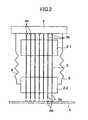
- FIG. 2is a diagram showing a state in which the contactor of FIG. 1 is disposed between an electronic component and a probe substrate;
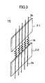
- FIG. 3is an oblique view showing a modification of the contactor of FIG. 1 ;
- FIG. 4is an oblique view showing the construction of a contactor according to a second embodiment of the present invention.
- FIGS. 5A and 5Bare oblique views showing a modification of the contactor of FIG. 4 ;
- FIG. 6is an oblique view showing a state in which the contactor of FIG. 5A was is disposed between a probe substrate and an electronic component;
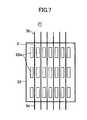
- FIG. 7is a front view showing the construction of a contactor according to a third embodiment of a present invention.
- FIG. 8is a front view showing a modification of the contactor of FIG. 7 ;
- FIG. 9is an oblique view showing the construction of a contactor according to a fourth embodiment of a present invention.
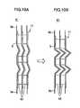
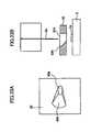
- FIGS. 10A and 10Bare side views of the contactor of FIG. 9 in two different states
- FIG. 11is a side view shows a first modification of the contactor shown in FIGS. 10A and 10B ;
- FIG. 12is a side view showing a second modification of the contactor shown in FIGS. 10 A and 10 B;
- FIGS. 13A and 13Bare oblique views showing examples of applying a processing to a substrate in relation to thermal expansion coefficient
- FIGS. 14A and 14Bare front views showing the construction of a contactor according to a sixth embodiment of the present invention.
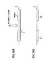
- FIGS. 15A and 15Bare diagrams explaining a process of making the contactor of FIG. 1 ;
- FIGS. 16A and 16Bare diagrams explaining a process of making of the contactor of FIG. 1 ;
- FIGS. 17A and 17Bare diagrams explaining a process of making of the contactor of FIG. 1 ;
- FIGS. 18A and 18Bare diagrams explaining a process of making of the contactor of FIG. 1 ;
- FIGS. 19A and 19Bare diagrams explaining a process of making of a contactor of FIG. 3 ;
- FIGS. 20A and 20Bare diagrams showing an example that uses an S-shaped form for the deformable part in the contactor of FIGS. 19A and 19B ;
- FIG. 21is a diagram showing an example of applying a heat treatment to the deformable part in the contactor of FIG. 20B ;
- FIG. 22is a diagram showing an example of providing an insulation coating on the deformable part of the contactor shown in FIG. 20B ;
- FIG. 23is an oblique view showing a modification of the contactor of FIG. 1 ;
- FIG. 24is an oblique view showing a modification of the contactor of FIG. 3 ;
- FIG. 25is a front view explaining the principle of a contactor according to a seventh embodiment of the present invention.
- FIGS. 26A and 26Bare cross-sectional view showing the form of a guide hole
- FIG. 27is a front view showing the contactor of FIG. 25 in the state in which the contactor is attached to a probe substrate;
- FIG. 28is a diagram showing an example of forming the contact terminal guide with a material having a coefficient of thermal expansion equivalent to that of a silicon wafer;
- FIG. 29is a diagram showing an example of forming the contact terminal guide with a material having a coefficient of thermal expansion equivalent to that of a seal material of a wafer-level CSP package;
- FIG. 30is a diagram showing an example of forming the contact terminal guide with a material having a coefficient of thermal expansion equivalent to that of a dicing film;
- FIG. 31a diagram showing an example of forming the contact terminal guide with a material having a coefficient of thermal expansion equivalent to that of a seal material of a semiconductor package;
- FIGS. 32A and 32Bare diagrams explaining a movement of a contact terminal on an electrode caused by thermal expansion
- FIGS. 33A and 33Bare diagrams explaining the form of a guide hole
- FIG. 34is a diagram showing a guide hole having a curved slope surface
- FIGS. 35A and 35Bare diagrams explaining another guide hole having a curved slope surface
- FIGS. 36A-36Care diagrams showing the construction of overlaying a contactor in alignment with the electrodes of a semiconductor device of peripheral type
- FIG. 37is a diagram showing the construction of a contactor in which the contactor has two rows of contact terminals in alignment of the electrodes of an area array type semiconductor device;
- FIG. 38is a diagram showing the construction of a contactor in which the contactor has contact terminals in alignment with the electrodes of an area array type semiconductor device;
- FIG. 39is a diagram showing the construction of a contactor adapted for a semiconductor device has two rows of electrodes along a peripheral part thereof;
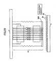
- FIG. 40is an oblique view showing the case in which the contactor has the wires in the form of microstrip line on a substrate;
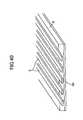
- FIG. 41is an oblique view showing a contactor in which the signal lines in the contactor are surrounded by ground wirings;
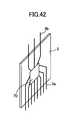
- FIG. 42is an oblique view showing an example in which an electronic component to the tested is mounted on a substrate of the contactor;
- FIG. 43is an oblique view showing the construction in which the pitch of the wires is changed on a substrate
- FIGS. 44A and 44Bare diagrams showing an example of applying a plating process to a tip end part of a contact terminal of a contactor
- FIGS. 45A and 45Bare diagrams showing an example in which a rough surface is formed on a tip end part the contact terminals.
- FIG. 46shows various examples of contact terminals and electrodes.
- FIG. 1is an oblique view of the contactor according to a first embodiment of a present invention.
- the contactor of the first embodiment of the present inventionis formed of two thin substrates 2 - 1 and 2 - 2 and a plurality of wires 3 .
- the substrates 2 - 1 and 2 - 2are thin substrates of an insulating material such as polyimide.
- the substrates 2 - 1 and 2 - 2are disposed in a spaced manner and the plural wires 3 are provided parallel with each other so as to connect the substrates 2 - 1 and 2 - 2 .
- the wires 3are formed of thin lines of a conductive metal such as copper.
- the wires 3are capable of causing elastic deformation to some extent.
- Each of the wires 3has an end part functioning as a contact terminal 3 a and another end part functioning as a contact terminal 3 b.
- FIG. 2is a diagram showing the state for the case the contactor of FIG. 1 is disposed between an electronic component and a probe substrate.
- a contactor 1is disposed between a probe substrate 4 and electronic component 5 .
- the probe substrate 4is a substrate located at the side of a circuit tester and is connected to a testing device not illustrated.
- the contact terminals 3 b of the contactor 1are arranged so as to make a contact with corresponding electrodes 4 a of the probe substrate 4 .
- the electronic component 5may be a semiconductor device (LSI etc.) to be tested and carries plural electrodes 5 a on a surface thereof. Thereby, the contact terminals 3 a of the wires 3 make a contact with the corresponding electrodes 5 a.
- the contactor 1is arranged between the probe substrate 4 and the electronic component 5 and the contact terminals 3 b of the wires 3 are contacted with the electrodes 4 a of the probe substrate 4 and the contact terminals 3 a are contacted with the electrode 5 a of the electronic component 5 .
- the electrodes 5 a of the electronic componentare connected to the probe substrate 4 and hence to the testing device electrically, and it becomes possible to conduct a test of the electronic component 5 while causing to flow an electric current to the electronic component 5 .
- each of the wires 3are arranged parallel with each other with an interval (pitch) identical with the interval of the electrodes 5 a of the electronic component 5 .
- the electronic component 5is an LSI of narrow electrode pitch and the electrodes 5 a are arranged with an interval of 40 ⁇ m, for example, each of the wires 3 may have a width of 20 ⁇ m and arranged with an interval of 20 ⁇ m. The process of forming the of contactor 1 will be explained later in detail.
- the contactor 1has a simple structure of including only the substrates 2 - 1 and 2 - 2 and the wires 3 , it is easy to form the wires 3 with a small pitch.
- the contactor of the present embodimentcan be used successfully to the semiconductor devices of narrow electrode pitch as in the above case.
- the contactor 1is contacted to the electronic component 5 in the state in which it is mounted on the probe substrate 4 .
- the contactor 1is fixed to the probe substrate 4 by mounting the substrate 2 - 2 of the contactor 1 on the probe substrate 4 by means of a support mechanism 6 .
- the support mechanism 6urges the contactor 1 to the probe substrate 4 such that the contact terminal 3 b s are contacted to the corresponding electrodes 4 a of the probe substrate 4 .
- the contactor 1is urged to the electronic component 5 and the contact terminals 3 a are contacted with the electrodes 5 a of the electronic component 5 .
- the wires 3undergo elastic deformation between the substrate 2 - 1 and the substrate 2 - 2 . Thereby, it becomes possible to achieve a positive contact between the contact terminals 3 a and the electrodes 5 a of the electronic component 5 and also between the contact terminals 3 b and electronic component 5 by the resilience of the wires 3 .
- the wires 3are formed of a thin band of a metal and has a relatively small spring constant. Therefore, an appropriate contact force is maintained even in the case the distance between the probe substrate 4 and the electronic component 5 is changed variously.
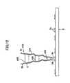
- FIG. 3is an oblique view diagram showing a contactor 1 A according to a modification of the abovementioned contactor 1 .
- the contactor 1 A of FIG. 3has a construction similar to that of the contactor 1 of FIG. 1 , except that there is provided a deforming part 3 c between the substrate 2 - 1 and the substrate 2 - 2 in each of the wires 3 .
- the deformable part 3 chas a zigzag form, and thus, the wire 3 easily extends or shrinks in the longitudinal direction thereof.
- the deformable part 3 cis not limited to the zigzag shape as shown in FIG. 3 but can take any other forms such as a trigonometric function form or U-shaped form, as long as it can be extended or compressed in the longitudinal direction of the wires 3 .
- FIG. 4is an oblique view diagram of a contactor 11 according to a second embodiment of a present invention.
- the contactor 11also has a construction similar to the abovementioned contactor 1 in that it is attached to the probe substrate 4 .
- the contactor 11is provided between the probe substrate 4 and the electronic component 5 .
- the explanation that overlaps with those explained beforewill be omitted.
- the wires 3are formed on a single substrate 12 , while the substrate 12 itself has a construction of causing a deformation.
- the wires 3undergo an elastic extension or contraction in the longitudinal direction thereof together with the substrate 12 .
- the wires 3undergo bending together with the deformation of the substrate 12 .
- the substrate 12is formed of an insulation material such as a thin polyimide film.
- the spring constant of the contactor 11is decided by the spring constant of the substrate 12 and the spring constant of the wires 3 .
- the spring constant of the substrate 12is large, it is preferable to provide a cut into the part of the substrate 12 that undergoes the deformation so as to facilitate the deformation.
- FIGS. 5A and 5Bare oblique view diagrams showing a contactor 11 A according to a further modification of the contactor 11 of FIG. 4 .
- an opening 12 a in the substrate 12 in the contactor 11 A of FIG. 5 Athere is provided an opening 12 a in the substrate 12 in the contactor 11 A of FIG. 5 A.
- the opening 12 ais formed in the part of the substrate 12 that undergoes syncline-mode deformation such that the wires 3 are bent inwardly. More specifically, the opening 12 a is provided to the substrate in correspondence to the part in which occurs accumulation of compressive strain and associated deformation in the substrate 12 . Thus, by cutting out the substrate 12 in correspondence to such a part, the deformation of the substrate 12 is substantially facilitated. Further, as shown in FIG. 6 , the wires 3 can deform or deflect freely without being constrained by the substrate 12 at the part where the opening 12 a is provided.
- the substrate 12 and the wires 3are deflected smoothly without applying unusual force to the wires 3 , and the overall spring constant of the contactor can be reduced.
- FIG. 7is a side view of the contactor according to a third embodiment of the present invention.
- the contactor 21 of the third embodimentincludes a single substrate 22 and plural wires 3 formed on the substrate 22 . Further, plural openings 22 a are provided in the substrate 21 . In the part of the substrate 22 in which the opening 22 a is provided, the rigidity of the substrate 223 is decreased, and it becomes possible to curve the substrate 21 easily together with the wires 3 . In other words, the spring constant of the contactor 21 is reduced by providing the opening 22 a , and the overall the spring constant of the contactor is reduced.
- the opening 22 a shown in FIG. 7is formed near the part of the substrate 22 in which the wires 3 are formed. Thereby, the substrate 22 is left in the part on which the wires 3 are provided.
- FIG. 8instead of forming the openings 22 a of 7 , it is also possible to form large openings 22 b so as to facilitate deformation of the wires 3 further. In this case, the wire 3 can be deformed freely without constraint by the substrate 22 , and the spring constant of contactor 21 A can be reduced further.
- FIG. 9is an oblique view of a contactor 31 according to a fourth embodiment of the present invention.
- the contactor 31includes a substrate 21 and plural wires 3 formed on the substrate 32 .
- the substrate 32is formed of a first substrate part 32 A and a second substrate part 32 B.
- the first substrate part 32 Ais formed by a material having a relatively large rigidity while the second substrate part 32 B is formed of a material having a smaller rigidity.
- the spring constant of the contactor as a wholeis primarily determined by the second substrate part 32 B. Further, the wires 3 are supported by the first substrate part 32 A and the second substrate part 32 B. Therefore, the separation of the adjacent wires 3 can be maintained constant. Contact of adjacent wires 3 can be prevented.
- FIGS. 10A and 10BNext, a fifth embodiment of the present invention will be described with reference to FIGS. 10A and 10B .
- FIGS. 10A and 10Bare side view diagrams of a contactor 41 according to the fifth embodiment respectively in a normal state where the contactor 41 is not deformed and in a deformed state in which the contactor 41 is deformed.
- the contactor 41is has a structure in which the contactors 11 of the second embodiment shown in FIG. 4 are overlaid with intervening spacers 42 .
- the spacer 42an insulating resin material or a resin film is suitable, while any insulating material that can support two of such substrates in a mutually separated state can be used for the spacer 42 . Thereby, the spacer 42 is fixed on the substrate 12 on the part that does not cause deformation.
- the contactor 41has plural wires 3 along the surface of the substrate 12 and a plurality of substrates 12 are stacked perpendicularly to the surface on which the wires 3 are provided. Thereby, it becomes possible to arrange the contact terminals 3 a and also the contact terminals 3 b in a two-dimensional, matrix state. Thereby, it becomes possible to test the semiconductor devices in which the electrode terminals are arranged in a two-dimensional array.
- FIG. 11is a side view diagram that showing a first modification of the contactor 41 shown in FIG. 10 .
- the contactor 41 Ahas a construction similar to that of FIGS. 10A and 10B in which the spacer 42 is replaced with a spacer 42 A of wide width.
- the spacer 42By changing the width of the spacer 42 like this, it becomes possible to change the arrangement of the contactor terminals 3 a and 3 b of the contactor in accordance with the arrangement of the terminals 5 a of the electronic component 5 .
- FIG. 12is a side view diagram showing a second modification of the contactor of FIGS. 10A and 10B .
- the contactor 41 Bhas a construction in which two contactors 11 are stacked with an angle by interposing spacers 42 B therebetween.
- the spacer 42 Bhas a narrow width in the part close to the contact terminals 3 a , while the width of the spacer 42 B increased toward the contactor terminals 3 b. Therefore, it becomes possible to secure a large pitch for the contact terminals 3 b while simultaneously making a contact with the electrodes 5 a of narrow pitch.
- FIG. 13Ait can be seen that there is formed a cut in the substrate 12 along the wires 3 as shown by dotted lines. Further, it is also possible to remove a part of the substrate 12 along the wires 3 with a predetermined width as shown in FIG. 13 B. Thereby, the substrate 12 is divided into a plurality of substrate pieces each corresponding to a wiring pattern 3 .
- the electronic component 5is a semiconductor device formed on a silicon wafer, for example, it is possible to set the amount of movement of the contact terminals 3 a , caused by thermal expansion of the contactor, to be equal to the amount of movement of the electrodes of the semiconductor device caused as a result of thermal expansion of the wafer, by forming the spacer 24 by silicon.
- FIGS. 14A and 14BNext, a sixth embodiment of the present invention will be described with reference to FIGS. 14A and 14B .
- FIGS. 14A and 14Bare side views of a contactor 51 according to the sixth embodiment of the present invention, wherein FIG. 14A shows the condition in which the contactor 51 is attached to the probe substrate 4 while FIG. 14B shows the state in which the contactor 51 is urged against the electrodes 5 a of the electronic apparatus 5 for making a contact.
- the contactor 51is the one corresponding to the contactor 1 A of FIG. 3 in which the substrate 2 - 2 is divided in correspondence to each of the wires 3 .
- each contact terminal 3 acan urge the corresponding electrode 5 a individually.
- the deformable part 3 cis extended in each of the wires 3 as shown in FIG. 14B , and it becomes possible to achieve an appropriate contact for all of the electrodes 5 a by the contact terminals 3 a.
- the first method of producing the contactor 1includes the step of forming the wires 3 on the substrate 12 as shown in FIG. 15 A. Further, the central part of the substrate 12 is removed thereafter as shown in FIG. 15 B.
- a resistis provided on the substrate 3 carrying the wires 3 , and the resist is removed from a part where the substrate 2 is to be removed. Further, the substrate 2 is removed by conducting an etching process or laser irradiation process at the part not covered by the resist. As a result, the contactor 1 is obtained as represented in FIG. 16 B.
- the second process of forming the contactor 1is to divide the substrate 1 into two pieces and then provide the wires 3 as represented in FIGS. 17A and 17B .
- the substrate 12is punched by using a mold into two separate pieces 2 - 1 and 2 - 2 , and the wires 3 are provided so as to bridge the substrates 2 - 1 and 2 - 2 as represented in FIG. 18 B.
- the wires 3may be formed of a copper wire, and the like.
- FIGS. 19A and 19Bare diagrams explains the process of producing the contactor 1 A of FIG. 3 .
- the wires 3are formed on the substrate 2 at first. It should be noted that such wires 3 include a deformable part 3 c of zigzag form, wherein such wires can be formed easily by etching a copper sheet attached on the substrate 2 by conducting an etching process.
- the substrate 2is separated into the substrates 2 - 1 and 2 - 2 according to the process similar to that of FIGS. 16A and 16B , and the contactor 1 A is obtained.
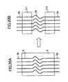
- FIGS. 20A and 20Bshow the example of the case in which the deformable part of the contactor 1 A is formed to have an S-shaped form.
- the process itselfis the same as in the process of FIGS. 19A and 19B .
- FIG. 21is a diagram showing the case of applying a thermal treatment or plating process to the deformable part 3 c of the wires 3 for the case of the contactor of FIGS. 20A and 20B .
- a thermal treatment or plating processto the deformable part 3 c of the wires 3 for the case of the contactor of FIGS. 20A and 20B .
- FIG. 22is a diagram showing the process of applying an insulation coating of polyimide resin, and the like, on the deformable part 3 c of the wires 3 for the case of the contactor of FIGS. 20A and 20B .
- an insulation coatingBy applying an insulation coating, it becomes possible not only to adjust the resiliency of the deformable part but also to eliminate short-circuit even in the case the deformable parts 3 c are contacted with each other.
- FIG. 23shows a modification of the contactor 1 in which the gap between the substrates 2 - 1 and 2 - 1 is filled with an elastic rubber resin such as a silicon rubber.
- FIG. 24shows an example similar to FIG. 22 in which the gap between the substrates 2 - 1 and 2 - 2 of the abovementioned contactor 1 A is filled with an elastic rubber resin like a silicon rubber.
- FIG. 25is a front view diagram explaining the principle of the contactor according to a seventh embodiment of the present invention.
- the contactor 61 shown in FIG. 25is formed of the contactor 1 A shown in FIG. 3 and a contact terminal guide 62 .
- the contact terminal guide 62has guide holes 62 a each being inserted with a corresponding contact terminal 3 a of the contactor 1 A.
- the contact terminal guide 62is disposed in the vicinity of the electrodes 5 a of the electronic component 5 to be tested and guides the contact terminals 3 a so that each terminal 3 a makes a correct contact with the corresponding electrode 5 a of the electronic component 5 .
- the guide holes 62 aare provided in the contact terminal guide 62 with the same arrangement of the electrodes of the electronic component 5 , and the contact terminals 3 a are positioned correctly in correspondence to the electrodes 5 a of the electronic component 5 by being inserted into the corresponding guide holes 62 a.
- FIGS. 26A and 26Bare cross-sectional diagrams showing the form of the guide hole 62 a.
- the guide hole 62 ahas sloped surfaces at both lateral sides thereof.
- the guide hole 62 a shown in FIG. 25Bhas a sloped surface on one side thereof. These sloped surfaces facilitate the insertion of the contact terminals 3 a and achieve an accurate positioning of the contact terminals 3 a.
- FIG. 27is a front view showing the contactor 61 in the state that the contactor 61 is attached on the probe substrate 4 .
- the substrate 2 - 1 of the contactor 1 Ais attached to the probe substrate 4 by a support mechanism.
- the terminal guide 62is attached to the probe substrate by the support mechanism 63 .
- the contact terminals 3 b of the contactor 1 Amake a contact to corresponding electrodes 4 a of the probe substrate.
- the contact terminals 3 aextend by penetrating through the corresponding guide holes 62 a of the guide 62 .
- the top end of the contact terminals 3 aprotrudes slightly from the guide hole 62 a.
- FIG. 28is a diagram showing the example in which the contact terminal guide 62 A is formed of a material identical with the silicon wafer or a material having a generally identical coefficient of thermal expansion, for the case in which a semiconductor device formed on a silicon wafer is used as the electronic component 5 to be tested.
- the contact terminals 3 a and the electrodes 5 amay be displaced relatively with each other at the time of high temperature test such as the burn-in test when there is a large difference of coefficient of thermal expansion between the electronic component (silicon wafer) and the substrate 2 - 2 of the contactor 1 A.
- the contact terminal 3 amisses the electrode 5 a.
- the contact terminal guide 62 Ais formed with the material having the same material of the electronic component (silicon wafer) or a material having a similar coefficient of thermal expansion, the amount of displacement with the thermal expansion becomes identical and the problem of relative displacement of the contact terminals 3 a and the electrodes 5 a disappears. Thereby, it becomes possible to align the contact terminals 3 a with the corresponding electrodes 5 a.
- FIG. 29shows the case in which the electronic component 5 is a wafer level CSP and the contact terminal guide 62 B is formed with a material having a coefficient of thermal expansion equivalent to that of the seal material or coating material of the wafer level CSP.
- the seal material of wafer level CSPincludes a mold resin of a package, a polyimide resin coating, a wire substrate, and the like.
- FIG. 30represents the case in which the electronic component 5 is a semiconductor device was attached to a dicing film and the contact terminal guide 62 C is formed of a material having a coefficient of thermal expansion equivalent to that of the dicing film.
- the dicing filmis formed of a comparatively cheap material of polyethylene and generally has a relatively large coefficient of thermal expansion.
- FIG. 31represents the case in which the electronic component 5 is a package semiconductor device formed of a simultaneous molding process.
- the contact terminal guide 62 Dis formed of a material having a coefficient of thermal expansion equivalent to that of the seal material or base material of the package semiconductor device.
- the base material of the package semiconductor devicemay be formed of a printed wire board, a TAB substrate, a ceramic substrate, and the like.
- the contact terminal guideBy properly selecting the material forming the contact terminal guide such that the contact terminal guide has a coefficient of thermal expansion equivalent to that of the test body as noted above, the problem of positional offset of the contact terminals 3 a by the thermal expansion effect is prevented and the test can be conducted with high reliability.
- the coefficient of thermal expansion of the contact terminal guide 62is set to be larger than the coefficient of thermal expansion of the electronic component 5 used for the test body as shown in FIG. 32A , for example, there occurs a movement of the contact terminals 3 a on the electrodes 5 a as a result of difference of the coefficient of thermal expansion as represented in FIG. 32 B. With this movement of the contact terminals 3 a , it is possible to attain the effect of reducing the contact resistance between the contact terminal 3 a and the electrode 5 a, by breaking the natural oxide film and the like formed on the contact electrode 5 a. Also, a similar effect can be achieved also in the case the coefficient of thermal expansion of the contact terminal guide 62 is smaller than the coefficient of thermal expansion of the electronic component 5 .
- FIGS. 33A and 33Bare diagrams explaining the form of the guide hole 62 a shown in FIGS. 26A and 26B , wherein FIG. 33A is a diagram showing the guide hole 62 a as viewed from the top direction while FIG. 26B is a diagram explains the guide of contact terminal 3 a.
- the guide hole 62 ais an elongated hole and a slope surface 62 b is extending from an end part thereof.
- a contact terminal 3 ais adjusted so as to locate right over a corresponding electrode 5 a of the electronic component 5 and makes a contact with the electrode 5 a by descending from the state illustrated in FIG. 33 B.
- the slope surface 62 bis not limited to a flat surface but may be a curved slope surface as shown in FIG. 34 . Further, it is also possible to provide a curved slope surface 62 b so as to surround the guide hole as shown in FIGS. 35A and 35B .
- FIGS. 36A-36Care diagrams explaining the effect of the abovementioned slope 62 b.
- FIG. 36Athere may be formed a deposit on the tip end of the contact terminal 3 a , wherein the deposit is removed from the contact terminal as a result of the tip end of the contact terminal 3 a sliding along the slope surface 62 b as shown in FIG. 36 B.
- FIG. 36Cthe tip end of the contact terminal 3 a , from which the deposits have been removed, is guided with certainty to the electrode 5 and achieves an excellent contact.
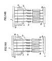
- FIG. 37is a diagram showing the construction in which the contactors noted above are stacked in conformity with the electrode arrangement of a peripheral type semiconductor device.
- FIG. 38is a diagram showing the construction in which the contact terminals 3 a are arranged in conformity with the electrode arrangement of an area array type semiconductor device.
- FIG. 39is a diagram showing the construction of the contactor adapted in conformity with a semiconductor device having the electrodes in two rows along a periphery thereof.
- FIG. 40is an oblique view showing the example in which the wires 3 are provided on the substrate 2 in the form of a microstrip line.
- the substrate 2is formed by a dielectric material and a conductor 2 b formed of Cu, for example, is provided on the entirety of on surface thereof as a ground surface.
- the wires 3are provided on the opposite surface by a patterning process of a copper layer, for example for example. With this, a contactor suitable for testing a semiconductor device that processes a high frequency signal.
- FIG. 42is an oblique view showing an example in which a testing component 70 is mounted on the substrate 2 of the contactor.
- the electronic component 70 thus testedmay be an A/D converter. According to such a construction, deterioration of the signal quality is prevented in the case an analog signal is supplied from the semiconductor to be tested, by converting the analog signal to a digital signal on the contactor. It is preferable to conduct such an A/D conversion in the part close to the tested body, and thus, it is preferable to provide the A/D converter on the contactor.
- FIG. 43is an oblique view showing the construction that changes the pitch of wires 3 on the substrate 2 .
- the pitch of the contact terminals 3 a at the side of the tested bodyis set to be smaller in conformity with the electrode pitch of the tested body.
- the pitch of the contact terminals 3 b at the side of the probe substrateis increased.
- Such a constructioncan be formed quite easily by forming the wires 3 of the contactor by conducting a patterning process.
- FIGS. 44A and 44Bare diagrams showing the example of performing a plating processing on a tip end part of the contact terminals 3 a. It should be noted that FIG. 44A shows the whole contactor. On the other hand, FIG. 44B is a diagram showing the part inside the circle that shown in FIG. 44A by a dotted line in an enlarged scale. The smaller the better for the contact resistance between the electrode of contactor terminal 3 a and electronic component 5 . For example, the contact resistance is reduced by forming a plating layer 71 of gold (Au), palladium (Pd), rhodium (Rd), platinum (Pt), and the like, on the contact terminals 3 a , which are formed of copper.
- Augold
- Pdpalladium
- Rdrhodium
- Ptplatinum
- the contact terminals 3 ahas a low affinity to the material of the electrode 5 a.
- the electrodes 5 aare generally formed of a solder. In such a case, it is preferable to apply nickel (Ni) plating at the tip end part of the contact terminals 3 a.
- the plating processis not limited to form a single plating layer but may include the process of forming plural plating layers.
- FIGS. 45A and 445Bare diagrams explaining the example for the case a rough surface is made at the tip end part of the contact terminals.
- FIG. 45Ashows the entire contact
- FIG. 45Bshows the contactor terminal inside the circle that shows in FIG. 45A by a dotted line in an enlarged scale.
- deposits or oxidation film formed on the electrode 5 a of the electronic component 5is removed effectively by providing such a rough surface of the tip end of the contact terminals 3 a.
- a rough surfacecan be formed by controlling the plating process or by dipping the plated tip end of the contact terminals 3 a into a chemical agent.
- FIG. 46is a diagram showing various examples of the tip end part of the contact terminal 3 a and the electrode 5 a of the electronic component 5 . Any of these shapes may be used for the tip end of the contact terminals 3 a in conformity with the shape of the electrode 5 a of the electronic component 5 .
- the wires 3 carrying the contact terminals 3 a thereonare formed by a patterning process, it should be noted that the contact terminals 3 a can be patterned into an arbitrary shape.
Landscapes
- Physics & Mathematics (AREA)
- General Physics & Mathematics (AREA)
- Measuring Leads Or Probes (AREA)
- Testing Of Individual Semiconductor Devices (AREA)
- Testing Or Measuring Of Semiconductors Or The Like (AREA)
Abstract
Description
Claims (32)
Applications Claiming Priority (2)
| Application Number | Priority Date | Filing Date | Title |
|---|---|---|---|
| JP2002002744AJP4391717B2 (en) | 2002-01-09 | 2002-01-09 | Contactor, manufacturing method thereof and contact method |
| JP2002-002744 | 2002-01-09 |
Publications (2)
| Publication Number | Publication Date |
|---|---|
| US20030127246A1 US20030127246A1 (en) | 2003-07-10 |
| US6927343B2true US6927343B2 (en) | 2005-08-09 |
Family
ID=19190783
Family Applications (1)
| Application Number | Title | Priority Date | Filing Date |
|---|---|---|---|
| US10/266,866Expired - LifetimeUS6927343B2 (en) | 2002-01-09 | 2002-10-09 | Contactor for testing miniaturized devices and components |
Country Status (5)
| Country | Link |
|---|---|
| US (1) | US6927343B2 (en) |
| JP (1) | JP4391717B2 (en) |
| KR (1) | KR100847034B1 (en) |
| CN (1) | CN1209806C (en) |
| TW (1) | TWI226932B (en) |
Cited By (45)
| Publication number | Priority date | Publication date | Assignee | Title |
|---|---|---|---|---|
| US20070068698A1 (en)* | 2005-09-26 | 2007-03-29 | Funai Electric Co., Ltd. | Flexible flat cable, method and apparatus for assembling the same |
| US7220920B1 (en)* | 2004-01-23 | 2007-05-22 | Hutchinson Technology Incorporated | Flexible electrical circuit with slotted coverlay |
| US20080029290A1 (en)* | 2006-08-02 | 2008-02-07 | Hon Hai Precision Ind. Co., Ltd. | Flexible flat cable with improved easy structures for engagement/disengagement |
| US20080083554A1 (en)* | 2006-10-04 | 2008-04-10 | International Business Machines Corporation | Hybrid bonded flex circuit |
| US20080298037A1 (en)* | 2007-02-19 | 2008-12-04 | Patent-Treuhand-Gesellschaft Fur Elektrische | Mounting panel arrangement |
| US20090236126A1 (en)* | 2006-08-29 | 2009-09-24 | Seiichiro Miyahara | Flexible Wiring Board |
| US20100212958A1 (en)* | 2007-09-18 | 2010-08-26 | Hans-Dieter Siems | Flexible electrical connection |
| US7837479B1 (en)* | 2009-07-16 | 2010-11-23 | Tyco Electronics Corporation | Mezzanine connector assembly having coated contacts |
| US20110272181A1 (en)* | 2010-05-07 | 2011-11-10 | Samsung Electronics Co., Ltd. | Multilayer Stretchable Cable |
| US20150011891A1 (en)* | 2012-03-27 | 2015-01-08 | Olympus Corporation | Cable connection structure, ultrasonic probe, and ultrasonic endoscope system |
| US20150019150A1 (en)* | 2011-03-28 | 2015-01-15 | Kabushiki Kaisha Toshiba | Semiconductor module |
| US20150065840A1 (en)* | 2013-08-30 | 2015-03-05 | Thalmic Labs Inc. | Systems, articles, and methods for stretchable printed circuit boards |
| US20160200269A1 (en)* | 2013-09-26 | 2016-07-14 | Yazaki Corporation | Wire harness |
| US9600030B2 (en) | 2014-02-14 | 2017-03-21 | Thalmic Labs Inc. | Systems, articles, and methods for elastic electrical cables and wearable electronic devices employing same |
| US9807221B2 (en) | 2014-11-28 | 2017-10-31 | Thalmic Labs Inc. | Systems, devices, and methods effected in response to establishing and/or terminating a physical communications link |
| US9880632B2 (en) | 2014-06-19 | 2018-01-30 | Thalmic Labs Inc. | Systems, devices, and methods for gesture identification |
| US10042422B2 (en) | 2013-11-12 | 2018-08-07 | Thalmic Labs Inc. | Systems, articles, and methods for capacitive electromyography sensors |
| US10078435B2 (en) | 2015-04-24 | 2018-09-18 | Thalmic Labs Inc. | Systems, methods, and computer program products for interacting with electronically displayed presentation materials |
| US10152082B2 (en) | 2013-05-13 | 2018-12-11 | North Inc. | Systems, articles and methods for wearable electronic devices that accommodate different user forms |
| US10188309B2 (en) | 2013-11-27 | 2019-01-29 | North Inc. | Systems, articles, and methods for electromyography sensors |
| US10199008B2 (en) | 2014-03-27 | 2019-02-05 | North Inc. | Systems, devices, and methods for wearable electronic devices as state machines |
| US10528135B2 (en) | 2013-01-14 | 2020-01-07 | Ctrl-Labs Corporation | Wearable muscle interface systems, devices and methods that interact with content displayed on an electronic display |
| US10593502B1 (en)* | 2018-08-21 | 2020-03-17 | Superior Essex International LP | Fusible continuous shields for use in communication cables |
| US10714874B1 (en) | 2015-10-09 | 2020-07-14 | Superior Essex International LP | Methods for manufacturing shield structures for use in communication cables |
| US10842407B2 (en) | 2018-08-31 | 2020-11-24 | Facebook Technologies, Llc | Camera-guided interpretation of neuromuscular signals |
| US10937414B2 (en) | 2018-05-08 | 2021-03-02 | Facebook Technologies, Llc | Systems and methods for text input using neuromuscular information |
| US10990174B2 (en) | 2016-07-25 | 2021-04-27 | Facebook Technologies, Llc | Methods and apparatus for predicting musculo-skeletal position information using wearable autonomous sensors |
| US11036302B1 (en) | 2018-05-08 | 2021-06-15 | Facebook Technologies, Llc | Wearable devices and methods for improved speech recognition |
| US20210242674A1 (en)* | 2018-04-23 | 2021-08-05 | Saint-Gobain Glass France | Long busbars having segments for increased robustness |
| US11170911B2 (en)* | 2018-05-25 | 2021-11-09 | Autonetworks Technologies, Ltd. | Wiring member |
| US11216069B2 (en) | 2018-05-08 | 2022-01-04 | Facebook Technologies, Llc | Systems and methods for improved speech recognition using neuromuscular information |
| US11426123B2 (en) | 2013-08-16 | 2022-08-30 | Meta Platforms Technologies, Llc | Systems, articles and methods for signal routing in wearable electronic devices that detect muscle activity of a user using a set of discrete and separately enclosed pod structures |
| US11481031B1 (en) | 2019-04-30 | 2022-10-25 | Meta Platforms Technologies, Llc | Devices, systems, and methods for controlling computing devices via neuromuscular signals of users |
| US11481030B2 (en) | 2019-03-29 | 2022-10-25 | Meta Platforms Technologies, Llc | Methods and apparatus for gesture detection and classification |
| US11493993B2 (en) | 2019-09-04 | 2022-11-08 | Meta Platforms Technologies, Llc | Systems, methods, and interfaces for performing inputs based on neuromuscular control |
| US11567573B2 (en) | 2018-09-20 | 2023-01-31 | Meta Platforms Technologies, Llc | Neuromuscular text entry, writing and drawing in augmented reality systems |
| US11635736B2 (en) | 2017-10-19 | 2023-04-25 | Meta Platforms Technologies, Llc | Systems and methods for identifying biological structures associated with neuromuscular source signals |
| US11644799B2 (en) | 2013-10-04 | 2023-05-09 | Meta Platforms Technologies, Llc | Systems, articles and methods for wearable electronic devices employing contact sensors |
| US20230154647A1 (en)* | 2020-04-06 | 2023-05-18 | Autonetworks Technologies, Ltd. | Wiring member |
| US11797087B2 (en) | 2018-11-27 | 2023-10-24 | Meta Platforms Technologies, Llc | Methods and apparatus for autocalibration of a wearable electrode sensor system |
| US11860193B2 (en) | 2018-11-21 | 2024-01-02 | Mitsui Chemicals, Inc. | Anisotropic conductive sheet, anisotropic conductive composite sheet, anisotropic conductive sheet set, electric inspection device and electric inspection method |
| US11868531B1 (en) | 2021-04-08 | 2024-01-09 | Meta Platforms Technologies, Llc | Wearable device providing for thumb-to-finger-based input gestures detected based on neuromuscular signals, and systems and methods of use thereof |
| US11907423B2 (en) | 2019-11-25 | 2024-02-20 | Meta Platforms Technologies, Llc | Systems and methods for contextualized interactions with an environment |
| US11921471B2 (en) | 2013-08-16 | 2024-03-05 | Meta Platforms Technologies, Llc | Systems, articles, and methods for wearable devices having secondary power sources in links of a band for providing secondary power in addition to a primary power source |
| US11961494B1 (en) | 2019-03-29 | 2024-04-16 | Meta Platforms Technologies, Llc | Electromagnetic interference reduction in extended reality environments |
Families Citing this family (32)
| Publication number | Priority date | Publication date | Assignee | Title |
|---|---|---|---|---|
| JP4721099B2 (en)* | 2004-03-16 | 2011-07-13 | 軍生 木本 | Electrical signal connection device, probe assembly and prober device using the same |
| FR2870382A1 (en)* | 2004-05-13 | 2005-11-18 | Commissariat Energie Atomique | ELASTIC CONNECTION WIRING |
| JP4727948B2 (en)* | 2004-05-24 | 2011-07-20 | 東京エレクトロン株式会社 | Multilayer substrate used for probe card |
| JP2008532042A (en)* | 2005-03-01 | 2008-08-14 | エス ヴィ プルーブ ピーティーイー リミテッド | Probe card having a multilayer substrate |
| JP4878438B2 (en)* | 2005-03-08 | 2012-02-15 | 東京特殊電線株式会社 | Probe needle and manufacturing method thereof |
| JP4649248B2 (en)* | 2005-03-22 | 2011-03-09 | 山一電機株式会社 | Probe unit |
| JP4962929B2 (en)* | 2005-09-19 | 2012-06-27 | 軍生 木本 | PROBER DEVICE AND PROBE ASSEMBLY USED FOR THE SAME |
| JP5077736B2 (en)* | 2005-09-19 | 2012-11-21 | 軍生 木本 | Contact assembly and LSI chip inspection apparatus using the same |
| US7737708B2 (en)* | 2006-05-11 | 2010-06-15 | Johnstech International Corporation | Contact for use in testing integrated circuits |
| US8422762B2 (en) | 2007-10-31 | 2013-04-16 | Advantest Corporation | Abnormality detecting apparatus for detecting abnormality at interface portion of contact arm |
| US7635973B2 (en)* | 2007-11-16 | 2009-12-22 | Electro Scientific Industries, Inc. | Electronic component handler test plate |
| JP5053106B2 (en)* | 2008-01-18 | 2012-10-17 | 株式会社石川技研 | Contact probe |
| JP5240827B2 (en)* | 2008-04-15 | 2013-07-17 | Necカシオモバイルコミュニケーションズ株式会社 | Flexible wiring board and electronic device |
| JP5333829B2 (en)* | 2008-10-03 | 2013-11-06 | 軍生 木本 | Probe assembly |
| JP5396112B2 (en)* | 2009-03-12 | 2014-01-22 | 東京エレクトロン株式会社 | Probe card |
| JP5079890B2 (en)* | 2011-01-05 | 2012-11-21 | 東京エレクトロン株式会社 | Multilayer substrate and probe card |
| GB2529346A (en) | 2011-03-31 | 2016-02-17 | Plasyl Ltd | Improvements for electrical circuits |
| JP6221234B2 (en)* | 2012-04-03 | 2017-11-01 | 大日本印刷株式会社 | Needle jig provided with a plurality of protruding needles and method for manufacturing the same |
| KR101438715B1 (en)* | 2013-02-26 | 2014-09-16 | 주식회사 오킨스전자 | Contact assembly having micro pitch, contact semi assembly, and preparation method thereof |
| US9231327B1 (en) | 2013-08-27 | 2016-01-05 | Flextronics Ap, Llc | Electronic circuit slidable interconnect |
| US9674949B1 (en) | 2013-08-27 | 2017-06-06 | Flextronics Ap, Llc | Method of making stretchable interconnect using magnet wires |
| US9801277B1 (en) | 2013-08-27 | 2017-10-24 | Flextronics Ap, Llc | Bellows interconnect |
| US9554465B1 (en) | 2013-08-27 | 2017-01-24 | Flextronics Ap, Llc | Stretchable conductor design and methods of making |
| US9521748B1 (en) | 2013-12-09 | 2016-12-13 | Multek Technologies, Ltd. | Mechanical measures to limit stress and strain in deformable electronics |
| US9338915B1 (en) | 2013-12-09 | 2016-05-10 | Flextronics Ap, Llc | Method of attaching electronic module on fabrics by stitching plated through holes |
| JP6346844B2 (en)* | 2014-11-04 | 2018-06-20 | 矢崎総業株式会社 | Conductive path connection member |
| JP5822042B1 (en)* | 2015-03-27 | 2015-11-24 | 日本電産リード株式会社 | Inspection jig, substrate inspection apparatus, and manufacturing method of inspection jig |
| US20190137541A1 (en)* | 2016-06-10 | 2019-05-09 | Hyung Ik KIM | Rubber socket and method for manufacturing same |
| CN109564244B (en) | 2016-07-28 | 2022-01-07 | 日本电产理德股份有限公司 | Inspection aid, substrate inspection device, and method for manufacturing inspection aid |
| KR101780747B1 (en) | 2017-03-31 | 2017-09-21 | 주식회사 더센 | Can Type Probe |
| KR101872817B1 (en)* | 2018-04-20 | 2018-06-29 | (주)에이치엠티 | Integral probe pin assembly for pin block |
| WO2022249954A1 (en)* | 2021-05-28 | 2022-12-01 | 株式会社日本マイクロニクス | Probe |
Citations (13)
| Publication number | Priority date | Publication date | Assignee | Title |
|---|---|---|---|---|
| US3168617A (en)* | 1962-08-27 | 1965-02-02 | Tape Cable Electronics Inc | Electric cables and method of making the same |
| US3837819A (en)* | 1968-04-10 | 1974-09-24 | Gen Electric | Zinc diffused copper |
| US4154977A (en)* | 1977-04-28 | 1979-05-15 | Akzona Incorporated | Multiconductor cable adapted for mass termination and for use in limited space |
| US4357750A (en)* | 1976-06-21 | 1982-11-09 | Advanced Circuit Technology Inc. | Jumper cable |
| US4406915A (en)* | 1981-04-10 | 1983-09-27 | Allied Corporation | Offset reformable jumper |
| US4616717A (en)* | 1978-11-09 | 1986-10-14 | Tel Tec Inc. | Flexible wire cable and process of making same |
| US5681662A (en)* | 1995-09-15 | 1997-10-28 | Olin Corporation | Copper alloy foils for flexible circuits |
| JPH10111316A (en) | 1996-10-04 | 1998-04-28 | Fujitsu Ltd | Semiconductor inspection apparatus and semiconductor inspection method |
| US5974662A (en)* | 1993-11-16 | 1999-11-02 | Formfactor, Inc. | Method of planarizing tips of probe elements of a probe card assembly |
| JPH11337579A (en) | 1998-05-25 | 1999-12-10 | Mitsubishi Materials Corp | Contact probe and probe device |
| US6110823A (en)* | 1993-11-16 | 2000-08-29 | Formfactor, Inc. | Method of modifying the thickness of a plating on a member by creating a temperature gradient on the member, applications for employing such a method, and structures resulting from such a method |
| US6515218B1 (en)* | 1999-11-22 | 2003-02-04 | Canon Kabushiki Kaisha | Photovoltaic element, process for the production thereof, method for removing a cover portion of a covered wire, and method for joining a covered wire and a conductor |
| US6531662B1 (en)* | 1999-04-22 | 2003-03-11 | Rohm Co., Ltd. | Circuit board, battery pack, and method of manufacturing circuit board |
Family Cites Families (10)
| Publication number | Priority date | Publication date | Assignee | Title |
|---|---|---|---|---|
| JPH03220787A (en)* | 1990-01-26 | 1991-09-27 | Yazaki Corp | Flexible circuit body and its manufacturing method |
| JPH0636620A (en)* | 1992-07-14 | 1994-02-10 | Nec Gumma Ltd | Flexible flat cable |
| JP3720887B2 (en)* | 1994-11-18 | 2005-11-30 | 富士通株式会社 | Contact device |
| JPH10104275A (en)* | 1996-09-30 | 1998-04-24 | Mitsubishi Materials Corp | Contact probe and probe device having the same |
| JP3749574B2 (en)* | 1996-07-16 | 2006-03-01 | ジェネシス・テクノロジー株式会社 | Probe card for semiconductor chip test |
| JP3268749B2 (en)* | 1997-01-29 | 2002-03-25 | 古河電気工業株式会社 | IC socket |
| JPH10239353A (en)* | 1997-02-27 | 1998-09-11 | Mitsubishi Materials Corp | Contact probe and probe apparatus with the same and manufacture for contact probe |
| JP3219032B2 (en)* | 1997-10-20 | 2001-10-15 | 日本電気株式会社 | probe |
| JPH11337574A (en)* | 1998-05-26 | 1999-12-10 | Takeda Sangyo Kk | Method of manufacturing probe unit |
| JP3059385U (en)* | 1998-11-26 | 1999-07-09 | 株式会社精研 | Inspection probe |
- 2002
- 2002-01-09JPJP2002002744Apatent/JP4391717B2/ennot_activeExpired - Fee Related
- 2002-10-09USUS10/266,866patent/US6927343B2/ennot_activeExpired - Lifetime
- 2002-10-14TWTW091123611Apatent/TWI226932B/ennot_activeIP Right Cessation
- 2002-10-23KRKR1020020064807Apatent/KR100847034B1/ennot_activeExpired - Fee Related
- 2002-11-01CNCNB021479968Apatent/CN1209806C/ennot_activeExpired - Fee Related
Patent Citations (13)
| Publication number | Priority date | Publication date | Assignee | Title |
|---|---|---|---|---|
| US3168617A (en)* | 1962-08-27 | 1965-02-02 | Tape Cable Electronics Inc | Electric cables and method of making the same |
| US3837819A (en)* | 1968-04-10 | 1974-09-24 | Gen Electric | Zinc diffused copper |
| US4357750A (en)* | 1976-06-21 | 1982-11-09 | Advanced Circuit Technology Inc. | Jumper cable |
| US4154977A (en)* | 1977-04-28 | 1979-05-15 | Akzona Incorporated | Multiconductor cable adapted for mass termination and for use in limited space |
| US4616717A (en)* | 1978-11-09 | 1986-10-14 | Tel Tec Inc. | Flexible wire cable and process of making same |
| US4406915A (en)* | 1981-04-10 | 1983-09-27 | Allied Corporation | Offset reformable jumper |
| US5974662A (en)* | 1993-11-16 | 1999-11-02 | Formfactor, Inc. | Method of planarizing tips of probe elements of a probe card assembly |
| US6110823A (en)* | 1993-11-16 | 2000-08-29 | Formfactor, Inc. | Method of modifying the thickness of a plating on a member by creating a temperature gradient on the member, applications for employing such a method, and structures resulting from such a method |
| US5681662A (en)* | 1995-09-15 | 1997-10-28 | Olin Corporation | Copper alloy foils for flexible circuits |
| JPH10111316A (en) | 1996-10-04 | 1998-04-28 | Fujitsu Ltd | Semiconductor inspection apparatus and semiconductor inspection method |
| JPH11337579A (en) | 1998-05-25 | 1999-12-10 | Mitsubishi Materials Corp | Contact probe and probe device |
| US6531662B1 (en)* | 1999-04-22 | 2003-03-11 | Rohm Co., Ltd. | Circuit board, battery pack, and method of manufacturing circuit board |
| US6515218B1 (en)* | 1999-11-22 | 2003-02-04 | Canon Kabushiki Kaisha | Photovoltaic element, process for the production thereof, method for removing a cover portion of a covered wire, and method for joining a covered wire and a conductor |
Cited By (67)
| Publication number | Priority date | Publication date | Assignee | Title |
|---|---|---|---|---|
| US7220920B1 (en)* | 2004-01-23 | 2007-05-22 | Hutchinson Technology Incorporated | Flexible electrical circuit with slotted coverlay |
| US7312398B2 (en)* | 2005-09-26 | 2007-12-25 | Funai Electric Co., Ltd. | Flexible flat cable, method and apparatus for assembling the same |
| US20070068698A1 (en)* | 2005-09-26 | 2007-03-29 | Funai Electric Co., Ltd. | Flexible flat cable, method and apparatus for assembling the same |
| US20080029290A1 (en)* | 2006-08-02 | 2008-02-07 | Hon Hai Precision Ind. Co., Ltd. | Flexible flat cable with improved easy structures for engagement/disengagement |
| US7696440B2 (en)* | 2006-08-02 | 2010-04-13 | Hon Hai Precision Ind. Co., Ltd. | Flexible flat cable with improved easy structures for engagement/disengagement |
| US20090236126A1 (en)* | 2006-08-29 | 2009-09-24 | Seiichiro Miyahara | Flexible Wiring Board |
| US8242373B2 (en)* | 2006-08-29 | 2012-08-14 | Nippon Mektron, Ltd. | Flexible wiring board with characteristic impedance control circuit |
| US20080083554A1 (en)* | 2006-10-04 | 2008-04-10 | International Business Machines Corporation | Hybrid bonded flex circuit |
| US8217277B2 (en)* | 2007-02-19 | 2012-07-10 | Osram Ag | Mounting panel arrangement |
| US20080298037A1 (en)* | 2007-02-19 | 2008-12-04 | Patent-Treuhand-Gesellschaft Fur Elektrische | Mounting panel arrangement |
| US8889991B2 (en)* | 2007-09-18 | 2014-11-18 | Robert Bosch Gmbh | Flexible electrical connection |
| US20100212958A1 (en)* | 2007-09-18 | 2010-08-26 | Hans-Dieter Siems | Flexible electrical connection |
| US7837479B1 (en)* | 2009-07-16 | 2010-11-23 | Tyco Electronics Corporation | Mezzanine connector assembly having coated contacts |
| US8624124B2 (en)* | 2010-05-07 | 2014-01-07 | Samsung Electronics Co., Ltd | Multilayer stretchable cable |
| US20110272181A1 (en)* | 2010-05-07 | 2011-11-10 | Samsung Electronics Co., Ltd. | Multilayer Stretchable Cable |
| US20150019150A1 (en)* | 2011-03-28 | 2015-01-15 | Kabushiki Kaisha Toshiba | Semiconductor module |
| US9772359B2 (en)* | 2011-03-28 | 2017-09-26 | Kabushiki Kaisha Toshiba | Semiconductor module |
| US10158188B2 (en)* | 2012-03-27 | 2018-12-18 | Olympus Corporation | Cable connection structure, ultrasonic probe, and ultrasonic endoscope system |
| US20150011891A1 (en)* | 2012-03-27 | 2015-01-08 | Olympus Corporation | Cable connection structure, ultrasonic probe, and ultrasonic endoscope system |
| US11009951B2 (en) | 2013-01-14 | 2021-05-18 | Facebook Technologies, Llc | Wearable muscle interface systems, devices and methods that interact with content displayed on an electronic display |
| US10528135B2 (en) | 2013-01-14 | 2020-01-07 | Ctrl-Labs Corporation | Wearable muscle interface systems, devices and methods that interact with content displayed on an electronic display |
| US10152082B2 (en) | 2013-05-13 | 2018-12-11 | North Inc. | Systems, articles and methods for wearable electronic devices that accommodate different user forms |
| US11921471B2 (en) | 2013-08-16 | 2024-03-05 | Meta Platforms Technologies, Llc | Systems, articles, and methods for wearable devices having secondary power sources in links of a band for providing secondary power in addition to a primary power source |
| US11426123B2 (en) | 2013-08-16 | 2022-08-30 | Meta Platforms Technologies, Llc | Systems, articles and methods for signal routing in wearable electronic devices that detect muscle activity of a user using a set of discrete and separately enclosed pod structures |
| US9788789B2 (en)* | 2013-08-30 | 2017-10-17 | Thalmic Labs Inc. | Systems, articles, and methods for stretchable printed circuit boards |
| US20150065840A1 (en)* | 2013-08-30 | 2015-03-05 | Thalmic Labs Inc. | Systems, articles, and methods for stretchable printed circuit boards |
| US20160200269A1 (en)* | 2013-09-26 | 2016-07-14 | Yazaki Corporation | Wire harness |
| US11644799B2 (en) | 2013-10-04 | 2023-05-09 | Meta Platforms Technologies, Llc | Systems, articles and methods for wearable electronic devices employing contact sensors |
| US10331210B2 (en) | 2013-11-12 | 2019-06-25 | North Inc. | Systems, articles, and methods for capacitive electromyography sensors |
| US10101809B2 (en) | 2013-11-12 | 2018-10-16 | Thalmic Labs Inc. | Systems, articles, and methods for capacitive electromyography sensors |
| US11079846B2 (en) | 2013-11-12 | 2021-08-03 | Facebook Technologies, Llc | Systems, articles, and methods for capacitive electromyography sensors |
| US10042422B2 (en) | 2013-11-12 | 2018-08-07 | Thalmic Labs Inc. | Systems, articles, and methods for capacitive electromyography sensors |
| US10310601B2 (en) | 2013-11-12 | 2019-06-04 | North Inc. | Systems, articles, and methods for capacitive electromyography sensors |
| US10188309B2 (en) | 2013-11-27 | 2019-01-29 | North Inc. | Systems, articles, and methods for electromyography sensors |
| US10362958B2 (en) | 2013-11-27 | 2019-07-30 | Ctrl-Labs Corporation | Systems, articles, and methods for electromyography sensors |
| US10251577B2 (en) | 2013-11-27 | 2019-04-09 | North Inc. | Systems, articles, and methods for electromyography sensors |
| US11666264B1 (en) | 2013-11-27 | 2023-06-06 | Meta Platforms Technologies, Llc | Systems, articles, and methods for electromyography sensors |
| US10898101B2 (en) | 2013-11-27 | 2021-01-26 | Facebook Technologies, Llc | Systems, articles, and methods for electromyography sensors |
| US9600030B2 (en) | 2014-02-14 | 2017-03-21 | Thalmic Labs Inc. | Systems, articles, and methods for elastic electrical cables and wearable electronic devices employing same |
| US10199008B2 (en) | 2014-03-27 | 2019-02-05 | North Inc. | Systems, devices, and methods for wearable electronic devices as state machines |
| US10684692B2 (en) | 2014-06-19 | 2020-06-16 | Facebook Technologies, Llc | Systems, devices, and methods for gesture identification |
| US9880632B2 (en) | 2014-06-19 | 2018-01-30 | Thalmic Labs Inc. | Systems, devices, and methods for gesture identification |
| US9807221B2 (en) | 2014-11-28 | 2017-10-31 | Thalmic Labs Inc. | Systems, devices, and methods effected in response to establishing and/or terminating a physical communications link |
| US10078435B2 (en) | 2015-04-24 | 2018-09-18 | Thalmic Labs Inc. | Systems, methods, and computer program products for interacting with electronically displayed presentation materials |
| US10714874B1 (en) | 2015-10-09 | 2020-07-14 | Superior Essex International LP | Methods for manufacturing shield structures for use in communication cables |
| US10990174B2 (en) | 2016-07-25 | 2021-04-27 | Facebook Technologies, Llc | Methods and apparatus for predicting musculo-skeletal position information using wearable autonomous sensors |
| US11635736B2 (en) | 2017-10-19 | 2023-04-25 | Meta Platforms Technologies, Llc | Systems and methods for identifying biological structures associated with neuromuscular source signals |
| US20210242674A1 (en)* | 2018-04-23 | 2021-08-05 | Saint-Gobain Glass France | Long busbars having segments for increased robustness |
| US12095251B2 (en)* | 2018-04-23 | 2024-09-17 | Saint-Gobain Glass France | Long busbars having segments for increased robustness |
| US10937414B2 (en) | 2018-05-08 | 2021-03-02 | Facebook Technologies, Llc | Systems and methods for text input using neuromuscular information |
| US11036302B1 (en) | 2018-05-08 | 2021-06-15 | Facebook Technologies, Llc | Wearable devices and methods for improved speech recognition |
| US11216069B2 (en) | 2018-05-08 | 2022-01-04 | Facebook Technologies, Llc | Systems and methods for improved speech recognition using neuromuscular information |
| US11170911B2 (en)* | 2018-05-25 | 2021-11-09 | Autonetworks Technologies, Ltd. | Wiring member |
| US10593502B1 (en)* | 2018-08-21 | 2020-03-17 | Superior Essex International LP | Fusible continuous shields for use in communication cables |
| US10905350B2 (en) | 2018-08-31 | 2021-02-02 | Facebook Technologies, Llc | Camera-guided interpretation of neuromuscular signals |
| US10842407B2 (en) | 2018-08-31 | 2020-11-24 | Facebook Technologies, Llc | Camera-guided interpretation of neuromuscular signals |
| US11567573B2 (en) | 2018-09-20 | 2023-01-31 | Meta Platforms Technologies, Llc | Neuromuscular text entry, writing and drawing in augmented reality systems |
| US11860193B2 (en) | 2018-11-21 | 2024-01-02 | Mitsui Chemicals, Inc. | Anisotropic conductive sheet, anisotropic conductive composite sheet, anisotropic conductive sheet set, electric inspection device and electric inspection method |
| US11797087B2 (en) | 2018-11-27 | 2023-10-24 | Meta Platforms Technologies, Llc | Methods and apparatus for autocalibration of a wearable electrode sensor system |
| US11941176B1 (en) | 2018-11-27 | 2024-03-26 | Meta Platforms Technologies, Llc | Methods and apparatus for autocalibration of a wearable electrode sensor system |
| US11481030B2 (en) | 2019-03-29 | 2022-10-25 | Meta Platforms Technologies, Llc | Methods and apparatus for gesture detection and classification |
| US11961494B1 (en) | 2019-03-29 | 2024-04-16 | Meta Platforms Technologies, Llc | Electromagnetic interference reduction in extended reality environments |
| US11481031B1 (en) | 2019-04-30 | 2022-10-25 | Meta Platforms Technologies, Llc | Devices, systems, and methods for controlling computing devices via neuromuscular signals of users |
| US11493993B2 (en) | 2019-09-04 | 2022-11-08 | Meta Platforms Technologies, Llc | Systems, methods, and interfaces for performing inputs based on neuromuscular control |
| US11907423B2 (en) | 2019-11-25 | 2024-02-20 | Meta Platforms Technologies, Llc | Systems and methods for contextualized interactions with an environment |
| US20230154647A1 (en)* | 2020-04-06 | 2023-05-18 | Autonetworks Technologies, Ltd. | Wiring member |
| US11868531B1 (en) | 2021-04-08 | 2024-01-09 | Meta Platforms Technologies, Llc | Wearable device providing for thumb-to-finger-based input gestures detected based on neuromuscular signals, and systems and methods of use thereof |
Also Published As
| Publication number | Publication date |
|---|---|
| CN1209806C (en) | 2005-07-06 |
| CN1431518A (en) | 2003-07-23 |
| JP4391717B2 (en) | 2009-12-24 |
| KR100847034B1 (en) | 2008-07-18 |
| JP2003207523A (en) | 2003-07-25 |
| US20030127246A1 (en) | 2003-07-10 |
| KR20030060751A (en) | 2003-07-16 |
| TWI226932B (en) | 2005-01-21 |
Similar Documents
| Publication | Publication Date | Title |
|---|---|---|
| US6927343B2 (en) | Contactor for testing miniaturized devices and components | |
| US6922069B2 (en) | Needle assembly of probe card | |
| TWI596346B (en) | Probe device of vertical probe card | |
| JP4496456B2 (en) | Prober equipment | |
| US5973394A (en) | Small contactor for test probes, chip packaging and the like | |
| JP5099487B2 (en) | Multi-beam composite contact | |
| US5189363A (en) | Integrated circuit testing system having a cantilevered contact lead probe pattern mounted on a flexible tape for interconnecting an integrated circuit to a tester | |
| US6791345B2 (en) | Contactor for testing semiconductor device and manufacturing method thereof | |
| JP4323055B2 (en) | Semiconductor device testing contactor and method of manufacturing the same | |
| US8427186B2 (en) | Probe element having a substantially zero stiffness and applications thereof | |
| US7898276B2 (en) | Probe card with stacked substrate | |
| JP4974021B2 (en) | Probe assembly | |
| US6511857B1 (en) | Process for manufacturing semiconductor device | |
| US7217139B2 (en) | Interconnect assembly for a probe card | |
| KR100340754B1 (en) | Connector apparatus | |
| JP2000156269A (en) | Socket for semiconductor | |
| WO2001096894A1 (en) | Compliant probe apparatus | |
| JP4962929B2 (en) | PROBER DEVICE AND PROBE ASSEMBLY USED FOR THE SAME | |
| JP2005127961A (en) | Substrate for tests and test equipment with its use | |
| KR200319202Y1 (en) | Needle assembly of probe card | |
| JPH11258269A (en) | Contactors for semiconductor devices | |
| WO2001084900A1 (en) | Connector apparatus | |
| JP2007157650A (en) | Socket for inspection device | |
| EP1698024A1 (en) | Small array contact with precision working range |
Legal Events
| Date | Code | Title | Description |
|---|---|---|---|
| AS | Assignment | Owner name:FUJITSU LIMITED, JAPAN Free format text:ASSIGNMENT OF ASSIGNORS INTEREST;ASSIGNORS:WATANABE, NAOYUKI;MARUYAMA, SHIGEYUKI;TASHIRO, KAZUHIRO;AND OTHERS;REEL/FRAME:013373/0664;SIGNING DATES FROM 20020618 TO 20020621 | |
| STCF | Information on status: patent grant | Free format text:PATENTED CASE | |
| FEPP | Fee payment procedure | Free format text:PAYOR NUMBER ASSIGNED (ORIGINAL EVENT CODE: ASPN); ENTITY STATUS OF PATENT OWNER: LARGE ENTITY | |
| AS | Assignment | Owner name:FUJITSU MICROELECTRONICS LIMITED, JAPAN Free format text:ASSIGNMENT OF ASSIGNORS INTEREST;ASSIGNOR:FUJITSU LIMITED;REEL/FRAME:021976/0089 Effective date:20081104 Owner name:FUJITSU MICROELECTRONICS LIMITED,JAPAN Free format text:ASSIGNMENT OF ASSIGNORS INTEREST;ASSIGNOR:FUJITSU LIMITED;REEL/FRAME:021976/0089 Effective date:20081104 | |
| FPAY | Fee payment | Year of fee payment:4 | |
| AS | Assignment | Owner name:FUJITSU SEMICONDUCTOR LIMITED, JAPAN Free format text:CHANGE OF NAME;ASSIGNOR:FUJITSU MICROELECTRONICS LIMITED;REEL/FRAME:024651/0744 Effective date:20100401 | |
| FPAY | Fee payment | Year of fee payment:8 | |
| AS | Assignment | Owner name:SOCIONEXT INC., JAPAN Free format text:ASSIGNMENT OF ASSIGNORS INTEREST;ASSIGNOR:FUJITSU SEMICONDUCTOR LIMITED;REEL/FRAME:035507/0923 Effective date:20150302 | |
| FPAY | Fee payment | Year of fee payment:12 |