US6925542B2 - Memory management in a data processing system - Google Patents
Memory management in a data processing systemDownload PDFInfo
- Publication number
- US6925542B2 US6925542B2US10/393,592US39359203AUS6925542B2US 6925542 B2US6925542 B2US 6925542B2US 39359203 AUS39359203 AUS 39359203AUS 6925542 B2US6925542 B2US 6925542B2
- Authority
- US
- United States
- Prior art keywords
- memory
- address
- access timing
- memory access
- processing system
- Prior art date
- Legal status (The legal status is an assumption and is not a legal conclusion. Google has not performed a legal analysis and makes no representation as to the accuracy of the status listed.)
- Expired - Lifetime
Links
Images


Classifications
- G—PHYSICS
- G06—COMPUTING OR CALCULATING; COUNTING
- G06F—ELECTRIC DIGITAL DATA PROCESSING
- G06F12/00—Accessing, addressing or allocating within memory systems or architectures
- G06F12/02—Addressing or allocation; Relocation
- G06F12/0223—User address space allocation, e.g. contiguous or non contiguous base addressing
- G06F12/0292—User address space allocation, e.g. contiguous or non contiguous base addressing using tables or multilevel address translation means
- G—PHYSICS
- G06—COMPUTING OR CALCULATING; COUNTING
- G06F—ELECTRIC DIGITAL DATA PROCESSING
- G06F12/00—Accessing, addressing or allocating within memory systems or architectures
- G—PHYSICS
- G06—COMPUTING OR CALCULATING; COUNTING
- G06F—ELECTRIC DIGITAL DATA PROCESSING
- G06F12/00—Accessing, addressing or allocating within memory systems or architectures
- G06F12/02—Addressing or allocation; Relocation
- G06F12/06—Addressing a physical block of locations, e.g. base addressing, module addressing, memory dedication
- G06F12/0646—Configuration or reconfiguration
- G06F12/0692—Multiconfiguration, e.g. local and global addressing
- Y—GENERAL TAGGING OF NEW TECHNOLOGICAL DEVELOPMENTS; GENERAL TAGGING OF CROSS-SECTIONAL TECHNOLOGIES SPANNING OVER SEVERAL SECTIONS OF THE IPC; TECHNICAL SUBJECTS COVERED BY FORMER USPC CROSS-REFERENCE ART COLLECTIONS [XRACs] AND DIGESTS
- Y02—TECHNOLOGIES OR APPLICATIONS FOR MITIGATION OR ADAPTATION AGAINST CLIMATE CHANGE
- Y02D—CLIMATE CHANGE MITIGATION TECHNOLOGIES IN INFORMATION AND COMMUNICATION TECHNOLOGIES [ICT], I.E. INFORMATION AND COMMUNICATION TECHNOLOGIES AIMING AT THE REDUCTION OF THEIR OWN ENERGY USE
- Y02D10/00—Energy efficient computing, e.g. low power processors, power management or thermal management
Definitions
- the present inventiongenerally relates to a data processing system, and more particularly, to memory management in a data processing system.
- a data processing systemmay include a variety of memories, some of which may have different timing specifications. Some of these memories may use a very small portion of the overall memory map. If the data processing system is used in a real-time application system, it may be useful during development to temporarily overlay small blocks of readily programmed memory (e.g. SRAM (static random access memory)) over a portion of more difficult to program memory (e.g. flash EEPROM (electrically erasable programmable read only memory) or ROM (read only memory)) in order to allow the values obtained from the memory to be temporarily changed more readily. Then when development has been completed, the final real-time system will use the more difficult to program memory instead of the SRAM which was used during development. Frequently the more difficult to program memory is formed on the same integrated circuit as other parts of the data processing system, while the more readily programmed memory used during development is formed on a separate integrated circuit.
- SRAMstatic random access memory
- more difficult to program memorye.g. flash EEPROM (electrically erasable programmable
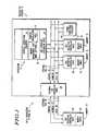
- FIG. 1illustrates, in block diagram form, a data processing system 10 in accordance with one embodiment of the present invention
- FIG. 2illustrates, in block diagram form, a memory address 50 in accordance with one embodiment of the present invention
- FIG. 3illustrates, in block diagram form, a memory map 70 in accordance with one embodiment of the present invention.
- FIG. 4illustrates, in block diagram form, an example of memory management unit (MMU) 16 translation in accordance with one embodiment of the present invention.
- MMUmemory management unit
- the memory used during developmente.g. off-chip SRAM
- the final real-time systeme.g. on-chip flash EEPROM, ROM
- reliabilityis more important that system speed performance.
- the regions of memory to be overlayed during developmentmay be scattered across the memory map.
- the granularity of blocks of the memory map for which it may be desirable to independently control timing specificationsmay be fairly fine.
- control registers to store memory timing specificationsmay require a prohibitively large number of control registers to be able to cover the scattered regions of memory.
- Another approach to independently specifying a timing characteristic of many scattered blocks of memorywas needed that did not required a large number of control registers.
- data processing system 10includes a processor 12 , memory 18 , memory 19 , other functional circuitry 20 , and external bus controller (EBC) 24 which are bi-directionally coupled by way of internal bus 22 .
- Internal bus 22includes control signals 26 , address signals 27 , and data signals 28 .
- Processor 12includes a bus interface controller (BIC) 13 which bi-directionally couples processor 12 to control signals 26 , address signals 27 , and data signals 28 .
- Memory 18includes a memory array 32 and a bus interface controller (BIC) 30 .
- BIC 30bi-directionally couples memory 18 to control signals 26 , address signals 27 , and data signals 28 .
- Memory 19includes a memory array 33 and a bus interface controller (BIC) 31 .
- BIC 31bi-directionally couples memory 19 to control signals 26 , address signals 27 , and data signals 28 .
- Other functional circuitry 20is bi-directionally coupled to control signals 26 , address signals 27 , and data signals 28 .
- External bus controller (EBC) 24is bi-directionally coupled to control signals 26 , address signals 27 , and data signals 28 .
- processor 12 , memory 18 , memory 19 , other functional circuitry 20 , and EBC 24may be coupled to any desired portions of internal bus 22 which allow these blocks to perform their respective functions.
- not all of the blocks 12 , 18 - 20 , and 24need to be coupled to all of the signals of internal bus 22 .
- at least a portion of control signals 26 and 36may be used to transfer status information.
- Processor 12includes address generation circuitry 14 .
- Some embodiments of processor 12may include a memory management unit 16 .
- Memory management unit 16may include address translation table 9 .
- memory management unit 16is optional and address translation table 9 may be located anywhere appropriate in data processing system 10 , or itself may be optional.
- Other functional circuitry 20may perform any desired function. Some examples of functions which may be performed by other functional circuitry 20 are timers, an input/output port, a communications port (e.g. a serial communications port, a serial peripheral interface, etc.), drivers (e.g. LCD drivers), an analog-to-digital converter, a digital-to-analog converter, additional memory, a DMA device, or any other desired function.
- External bus controller (EBC) 24is used to bi-directionally couple internal bus 22 and external bus 35 .
- Integrated circuit 11is bi-directionally coupled to memory 34 by way of external bus 35 .
- External bus 35includes control signals 36 , address signals 37 , and data signal 38 .
- Memory 34includes a memory array 42 and a bus interface controller (BIC) 40 .
- BIC 40bi-directionally couples memory 34 to control signals 36 , address signals 37 , and data signals 38 .
- memory 34 and integrated circuit 11are implemented on different integrated circuits.
- various portions of data processing system 10are implemented on different integrated circuits or the same integrated circuit.
- memory 18 , 19 , and 34may have any desired number of memories implemented on integrated circuit 11 (e.g. memories 18 and 19 ) and any desired number of memories implemented external to integrated circuit 11 (e.g. memory 34 ).
- memory 18 , memory 19 , and memory 34may be any type of memory: including, but not limited to static random access memory (SRAM), dynamic random access memory (DRAM), read only memory (ROM), erasable programmable read only memory (EPROM), electrically erasable programmable read only memory (EEPROM), magnetic random access memory (MRAM), etc.
- SRAMstatic random access memory
- DRAMdynamic random access memory
- ROMread only memory
- EPROMerasable programmable read only memory
- EEPROMelectrically erasable programmable read only memory
- MRAMmagnetic random access memory
- memory address 50may be used to access any memory (e.g. 18 , 19 , 34 ) in data processing system 10 .
- Memory address 50may be provided by address generation circuit 14 within processor 12 , or may be provided by any other source of address generation within data processing system 10 , including other functional circuitry 20 .
- the lower order N-bits [ 0 - 23 ]are used as array index bits 52 to index into one of memory arrays 32 , 33 , or 42 .
- the next significant M-bits [ 24 - 28 ]are used as timing bits 54 to specify a timing parameter of one of memory arrays 32 , 33 , or 42 .
- timing bits 54include a plurality of timing parameters, such as a parameter specifying a number of primary wait states 53 [bits 26 - 28 ], and a parameter specifying a number of secondary wait states 55 [bits 24 - 25 ].
- Primary wait statesrefer to the wait states of an initial access in a burst of accesses.
- Secondary wait statesrefer to the wait states for one or more subsequent accesses in a burst of accesses. It is common for burst accesses to require different timing parameters for the different portions of the burst transfer.
- Alternate embodiments of the present inventionmay use timing bits 54 to specify any timing parameter of a memory in data processing system 10 .
- alternate embodiments of the present inventionmay use a portion of an access address (e.g. bits 54 ) to specify one or more non-timing parameters or attributes of the circuitry being accessed.
- the most significant L-bits [ 29 - 31 ]are used as device select bits 56 to select one of memory arrays 32 , 33 , or 42 .
- alternate embodiments of the present inventionmay partition memory address 50 into fewer, more, or different partitions, and the number of bits in each partition may vary as well.
- memory address 50 of FIG. 2now has a portion (timing bits 54 ) which are not used to differentiate between devices or storage locations within a device. These bits (timing bits 54 ) are instead used to specify a timing characteristic of the device selected by device select bits 56 .
- a memory arraye.g. 32 , 33 , 42
- the address bits 54 associated with the multiple-mappingare used to directly control timing parameters of the memory arrays (e.g. 32 , 33 , 42 ) with no indirect access to a control register required. This allows for flexible timing specification to be derived on an access by access basis without requiring any additional control storage overhead.
- Some embodiments of the present inventiontake advantage of the fact that the address space of a typical data processing system 10 is sparse, and thus multiple-mapping may be used and a portion of the memory address 50 used for accesses (e.g. timing bits 54 ) can be redirected for use as a timing specifier.
- a number of different values of address 50may be used to select the same location in memory. Selection of particular values for address 50 in which the timing bits 54 are different but in which the values of device select bits 56 are common, and array index bits 52 are common result in an access to the same location in memory, but using a different set of one or more timing parameters corresponding to timing bits 54 .
- the user of the data processing system 10may then directly control timing bits 54 to select a desired set of timing attributes independently of the actual data location in a memory array by generating appropriate values of memory address 50 .
- the present inventionallows the specification of memory timing parameters to be altered more efficiently as system conditions (e.g. operating clock frequency) are changed.
- the present inventiondoes not require the individual bus interface controllers ( 30 , 31 , 40 ) for each memory ( 18 , 19 , 34 ) to be reprogrammed when a system condition is changed.
- the timing bits 54 in the memory address 50itself are the only thing that must be modified by the user of data processing system 10 .
- the present inventionallows for faster transitions into different clocking modes which are relied upon for low power system operation. Low power system efficiency is thereby improved, since the transitions into and out of low power (low frequency) modes can be performed with lower software overhead, thus lowering the threshold for which a mode change is actually beneficial. With electronics being used in more and more handheld battery operated applications, any improvement that can reduce battery power consumption is important.
- FIG. 3illustrates one embodiment of a memory map 70 for memory array 32 of FIG. 1 .
- memory array 32is accessed by N array index bits 52 (see FIG. 2 ).
- Memory array 32thus has address locations 0 to 2 N ⁇ 1.
- Memory array 32can be mapped into memory map 70 multiple or a plurality of times as memory block 71 , 72 , and 73 .
- the array index bits 52 and the device select bits 56will be the same for each block 71 - 73 of FIG. 3 ; however, the timing bits 54 can be different or the same for each of blocks 71 - 73 .
- block 71can have a value 60 for timing bits 54
- block 72has a value 62 for timing bits 54
- block 73has a value 64 for timing bits 54 .
- Values 60 , 62 , and 64determine which of the multiple mappings of memory array 32 are used during an access.
- each block 71 - 73is the same size; however each block includes a different range of address locations in memory map 70 .
- the first block, block 71starts at address location 0 and ends at address location 2 N ⁇ 1.
- Block 72 and all other intervening blocksare each 2 N in size.
- the last block, block 73is 2 N in size and ends at address location each 2 N+M ⁇ 1, where M is the number of bits used for timing bits 54 (see FIG. 2 ).
- timing bits 54are available as timing bits 54 to specify a timing parameter on an access by access basis.
- timing bits 54are not needed to select the data stored in memory array 32 since the data appears in four different virtual copies due to the address aliasing. Instead, these two high-order bits are used to directly indicate a timing parameter (e.g.
- timing bits 54may be divided into a plurality of portions, where each portion may be used to specify a different timing parameter of memory array 32 .
- one or more portions of timing bits 54may specify non-timing related parameters.
- FIG. 4illustrates an example of memory management unit (MMU) 16 address translation (see FIG. 1 ).
- MMUmemory management unit
- logical address pages 90include page 80 , page 82 , and page 84 .
- each logical address page 80 , 82 , and 84may be mapped into a corresponding physical address page by MMU 16 .
- Each logical pagemay be mapped into any physical page, giving complete flexibility in assigning a physical page address to a corresponding logical page address.
- the physical address pages 92correspond to 4 different blocks (e.g. blocks like 71 - 73 in FIG.
- Timing bits 54applies to physical address pages 80 a , 82 a , and 84 a .
- Value 101 for timing bits 54applies to physical address pages 80 b , 82 b , and 84 b .
- blocks 60 , 61 , 62 , and 64occupy the next blocks of physical addresses.
- Value 102 for timing bits 54applies to physical address pages 80 c , 82 c , and 84 c .
- Value 103 for timing bits 54applies to physical address pages 80 d , 82 d , and 84 d.
- an MMU 16is not required to practice the present invention, but that the present invention may indeed be used when an MMU 16 is utilized.
- One advantage of utilizing an MMUis that the logical to physical address mapping may be used to change the mapping of a logical page in order to select a different value for timing bits 54 with no program modification of logical addresses, and utilizing the already existing capability of address translation table 9 of FIG. 1 .
- value 100is used for timing bits 54 .
- logical page 84may be mapped to physical page 84 b to select value 101 for timing bits 54 .
- the same value in memory array 32is accessed, since memory array 32 is multiple-mapped to multiple locations in physical address space (physical address pages 92 ), each multiple mapping corresponding to a different value for timing bits 54 .
- timing bits 54 associated with the multiple-mappingsmay be used for other control purposes such as controlling an operating mode of one or more portions of data processing system 10 , or controlling a response from one or more elements of data processing system 10 .
Landscapes
- Engineering & Computer Science (AREA)
- Theoretical Computer Science (AREA)
- Physics & Mathematics (AREA)
- General Engineering & Computer Science (AREA)
- General Physics & Mathematics (AREA)
- Memory System (AREA)
Abstract
Description
Claims (21)
Priority Applications (6)
| Application Number | Priority Date | Filing Date | Title |
|---|---|---|---|
| US10/393,592US6925542B2 (en) | 2003-03-21 | 2003-03-21 | Memory management in a data processing system |
| TW092135578ATWI309771B (en) | 2003-03-21 | 2003-12-16 | Managing method for controlling operating parameter and/or memory access timing in a data processing system and/or relevant data processing system |
| PCT/US2004/003093WO2004095288A1 (en) | 2003-03-21 | 2004-02-04 | Memory management in a data processing system |
| KR1020057017279AKR20050110006A (en) | 2003-03-21 | 2004-02-04 | Memory management in a data processing system |
| JP2006508655AJP4700604B2 (en) | 2003-03-21 | 2004-02-04 | Memory management in data processing systems |
| EP04708127AEP1609067A4 (en) | 2003-03-21 | 2004-02-04 | Memory management in a data processing system |
Applications Claiming Priority (1)
| Application Number | Priority Date | Filing Date | Title |
|---|---|---|---|
| US10/393,592US6925542B2 (en) | 2003-03-21 | 2003-03-21 | Memory management in a data processing system |
Publications (2)
| Publication Number | Publication Date |
|---|---|
| US20040186973A1 US20040186973A1 (en) | 2004-09-23 |
| US6925542B2true US6925542B2 (en) | 2005-08-02 |
Family
ID=32988183
Family Applications (1)
| Application Number | Title | Priority Date | Filing Date |
|---|---|---|---|
| US10/393,592Expired - LifetimeUS6925542B2 (en) | 2003-03-21 | 2003-03-21 | Memory management in a data processing system |
Country Status (6)
| Country | Link |
|---|---|
| US (1) | US6925542B2 (en) |
| EP (1) | EP1609067A4 (en) |
| JP (1) | JP4700604B2 (en) |
| KR (1) | KR20050110006A (en) |
| TW (1) | TWI309771B (en) |
| WO (1) | WO2004095288A1 (en) |
Cited By (2)
| Publication number | Priority date | Publication date | Assignee | Title |
|---|---|---|---|---|
| US20070198805A1 (en)* | 2006-02-23 | 2007-08-23 | Richard Soja | Non-intrusive address mapping having a modified address space identifier and circuitry therefor |
| US20070255924A1 (en)* | 2006-04-28 | 2007-11-01 | Moyer William C | Processor and method for altering address translation |
Families Citing this family (5)
| Publication number | Priority date | Publication date | Assignee | Title |
|---|---|---|---|---|
| US9304773B2 (en)* | 2006-03-21 | 2016-04-05 | Freescale Semiconductor, Inc. | Data processor having dynamic control of instruction prefetch buffer depth and method therefor |
| US20120230395A1 (en)* | 2011-03-11 | 2012-09-13 | Louis Joseph Kerofsky | Video decoder with reduced dynamic range transform with quantization matricies |
| JP2016520226A (en)* | 2013-05-16 | 2016-07-11 | アドバンスト・マイクロ・ディバイシズ・インコーポレイテッドAdvanced Micro Devices Incorporated | Memory system with region specific memory access scheduling |
| KR20150044370A (en)* | 2013-10-16 | 2015-04-24 | 삼성전자주식회사 | Systems for managing heterogeneous memories |
| KR20170059239A (en)* | 2015-11-20 | 2017-05-30 | 삼성전자주식회사 | Memory device and memory system having heterogeneous memories |
Citations (9)
| Publication number | Priority date | Publication date | Assignee | Title |
|---|---|---|---|---|
| US5418924A (en)* | 1992-08-31 | 1995-05-23 | Hewlett-Packard Company | Memory controller with programmable timing |
| US5440710A (en)* | 1994-03-08 | 1995-08-08 | Exponential Technology, Inc. | Emulation of segment bounds checking using paging with sub-page validity |
| US5553144A (en)* | 1993-03-11 | 1996-09-03 | International Business Machines Corporation | Method and system for selectively altering data processing system functional characteristics without mechanical manipulation |
| US5623648A (en) | 1995-08-30 | 1997-04-22 | National Semiconductor Corporation | Controller for initiating insertion of wait states on a signal bus |
| US5809340A (en)* | 1993-04-30 | 1998-09-15 | Packard Bell Nec | Adaptively generating timing signals for access to various memory devices based on stored profiles |
| US6073223A (en) | 1997-07-21 | 2000-06-06 | Hewlett-Packard Company | Memory controller and method for intermittently activating and idling a clock signal for a synchronous memory |
| USRE37305E1 (en)* | 1982-12-30 | 2001-07-31 | International Business Machines Corporation | Virtual memory address translation mechanism with controlled data persistence |
| US6438670B1 (en)* | 1998-10-02 | 2002-08-20 | International Business Machines Corporation | Memory controller with programmable delay counter for tuning performance based on timing parameter of controlled memory storage device |
| US6505282B1 (en)* | 1994-11-30 | 2003-01-07 | Intel Corporation | Method and apparatus for determining memory types of a multi-type memory subsystem where memory of the different types are accessed using column control signals with different timing characteristics |
Family Cites Families (2)
| Publication number | Priority date | Publication date | Assignee | Title |
|---|---|---|---|---|
| JPH10208468A (en)* | 1997-01-28 | 1998-08-07 | Hitachi Ltd | Semiconductor storage device and synchronous semiconductor storage device |
| US6282626B1 (en)* | 1999-07-15 | 2001-08-28 | 3Com Corporation | No stall read access-method for hiding latency in processor memory accesses |
- 2003
- 2003-03-21USUS10/393,592patent/US6925542B2/ennot_activeExpired - Lifetime
- 2003-12-16TWTW092135578Apatent/TWI309771B/ennot_activeIP Right Cessation
- 2004
- 2004-02-04JPJP2006508655Apatent/JP4700604B2/ennot_activeExpired - Fee Related
- 2004-02-04KRKR1020057017279Apatent/KR20050110006A/ennot_activeCeased
- 2004-02-04EPEP04708127Apatent/EP1609067A4/ennot_activeWithdrawn
- 2004-02-04WOPCT/US2004/003093patent/WO2004095288A1/enactiveApplication Filing
Patent Citations (10)
| Publication number | Priority date | Publication date | Assignee | Title |
|---|---|---|---|---|
| USRE37305E1 (en)* | 1982-12-30 | 2001-07-31 | International Business Machines Corporation | Virtual memory address translation mechanism with controlled data persistence |
| US5418924A (en)* | 1992-08-31 | 1995-05-23 | Hewlett-Packard Company | Memory controller with programmable timing |
| US5553144A (en)* | 1993-03-11 | 1996-09-03 | International Business Machines Corporation | Method and system for selectively altering data processing system functional characteristics without mechanical manipulation |
| US5809340A (en)* | 1993-04-30 | 1998-09-15 | Packard Bell Nec | Adaptively generating timing signals for access to various memory devices based on stored profiles |
| US5440710A (en)* | 1994-03-08 | 1995-08-08 | Exponential Technology, Inc. | Emulation of segment bounds checking using paging with sub-page validity |
| US6505282B1 (en)* | 1994-11-30 | 2003-01-07 | Intel Corporation | Method and apparatus for determining memory types of a multi-type memory subsystem where memory of the different types are accessed using column control signals with different timing characteristics |
| US5623648A (en) | 1995-08-30 | 1997-04-22 | National Semiconductor Corporation | Controller for initiating insertion of wait states on a signal bus |
| US6073223A (en) | 1997-07-21 | 2000-06-06 | Hewlett-Packard Company | Memory controller and method for intermittently activating and idling a clock signal for a synchronous memory |
| US6438670B1 (en)* | 1998-10-02 | 2002-08-20 | International Business Machines Corporation | Memory controller with programmable delay counter for tuning performance based on timing parameter of controlled memory storage device |
| US6453434B2 (en)* | 1998-10-02 | 2002-09-17 | International Business Machines Corporation | Dynamically-tunable memory controller |
Cited By (6)
| Publication number | Priority date | Publication date | Assignee | Title |
|---|---|---|---|---|
| US20070198805A1 (en)* | 2006-02-23 | 2007-08-23 | Richard Soja | Non-intrusive address mapping having a modified address space identifier and circuitry therefor |
| US20070198804A1 (en)* | 2006-02-23 | 2007-08-23 | Moyer William C | Data processing system having address translation bypass and method therefor |
| US7376807B2 (en) | 2006-02-23 | 2008-05-20 | Freescale Semiconductor, Inc. | Data processing system having address translation bypass and method therefor |
| US7447867B2 (en) | 2006-02-23 | 2008-11-04 | Freescale Semiconductor, Inc. | Non-intrusive address mapping having a modified address space identifier and circuitry therefor |
| US20070255924A1 (en)* | 2006-04-28 | 2007-11-01 | Moyer William C | Processor and method for altering address translation |
| US7401201B2 (en) | 2006-04-28 | 2008-07-15 | Freescale Semiconductor, Inc. | Processor and method for altering address translation |
Also Published As
| Publication number | Publication date |
|---|---|
| KR20050110006A (en) | 2005-11-22 |
| WO2004095288A1 (en) | 2004-11-04 |
| TWI309771B (en) | 2009-05-11 |
| US20040186973A1 (en) | 2004-09-23 |
| JP2006520969A (en) | 2006-09-14 |
| EP1609067A1 (en) | 2005-12-28 |
| JP4700604B2 (en) | 2011-06-15 |
| TW200506603A (en) | 2005-02-16 |
| EP1609067A4 (en) | 2008-04-16 |
Similar Documents
| Publication | Publication Date | Title |
|---|---|---|
| US10552145B2 (en) | Memory devices, systems, and methods for updating firmware with single memory device | |
| US7657696B2 (en) | Method to detect NAND-flash parameters by hardware automatically | |
| JP3670041B2 (en) | Nonvolatile memory chip enable encoding method, computer system, and memory controller | |
| EP2480976A2 (en) | Memory device and method | |
| CN112602066A (en) | Forward cache memory system and method | |
| KR19980033054A (en) | Programmable Memory Access | |
| US7343469B1 (en) | Remapping I/O device addresses into high memory using GART | |
| US6925542B2 (en) | Memory management in a data processing system | |
| EP1984827A1 (en) | An electronic device having a memory element and method of operation therefor | |
| US11537389B2 (en) | Memory devices, systems, and methods for updating firmware with single memory device | |
| JP5856434B2 (en) | Bus connection circuit, semiconductor device, and operation method of bus connection circuit | |
| US20090049269A1 (en) | Host memory interface for a parallel processor | |
| KR102254066B1 (en) | Forward caching application programming interface system and method | |
| US20070283139A1 (en) | Information processing apparatus and control method used thereby | |
| US5592652A (en) | Single-chip microcomputer system having address space allocation hardware for different modes | |
| US7376791B2 (en) | Memory access systems and methods for configuring ways as cache or directly addressable memory | |
| EP1164490B1 (en) | Re-configurable memory map for a system on a chip | |
| CN107977325B (en) | Memory controller, memory system and method of operating a memory controller | |
| US7124261B2 (en) | Access to bit values within data words stored in a memory | |
| US20040250006A1 (en) | Method of accessing data of a computer system | |
| US7228367B2 (en) | Direct memory access controller for carrying out data transfer by determining whether or not burst access can be utilized in an external bus and access control method thereof | |
| US6327640B1 (en) | Overlapping peripheral chip select space with DRAM on a microcontroller with an integrated DRAM controller | |
| KR900005315A (en) | Development Method of Data Processing System and Semiconductor Integrated Circuits for Data Processing | |
| US5752267A (en) | Data processing system for accessing an external device during a burst mode of operation and method therefor | |
| KR20030057916A (en) | System for Device Chip Selection in Common Bus Structure |
Legal Events
| Date | Code | Title | Description |
|---|---|---|---|
| AS | Assignment | Owner name:MOTOROLA, INC., ILLINOIS Free format text:ASSIGNMENT OF ASSIGNORS INTEREST;ASSIGNORS:MOYER, WILLIAM C.;MARSHALL, RAY;REEL/FRAME:013898/0804;SIGNING DATES FROM 20030313 TO 20030318 | |
| AS | Assignment | Owner name:FREESCALE SEMICONDUCTOR, INC., TEXAS Free format text:ASSIGNMENT OF ASSIGNORS INTEREST;ASSIGNOR:MOTOROLA, INC;REEL/FRAME:015360/0718 Effective date:20040404 Owner name:FREESCALE SEMICONDUCTOR, INC.,TEXAS Free format text:ASSIGNMENT OF ASSIGNORS INTEREST;ASSIGNOR:MOTOROLA, INC;REEL/FRAME:015360/0718 Effective date:20040404 | |
| STCF | Information on status: patent grant | Free format text:PATENTED CASE | |
| AS | Assignment | Owner name:CITIBANK, N.A. AS COLLATERAL AGENT, NEW YORK Free format text:SECURITY AGREEMENT;ASSIGNORS:FREESCALE SEMICONDUCTOR, INC.;FREESCALE ACQUISITION CORPORATION;FREESCALE ACQUISITION HOLDINGS CORP.;AND OTHERS;REEL/FRAME:018855/0129 Effective date:20061201 Owner name:CITIBANK, N.A. AS COLLATERAL AGENT,NEW YORK Free format text:SECURITY AGREEMENT;ASSIGNORS:FREESCALE SEMICONDUCTOR, INC.;FREESCALE ACQUISITION CORPORATION;FREESCALE ACQUISITION HOLDINGS CORP.;AND OTHERS;REEL/FRAME:018855/0129 Effective date:20061201 | |
| CC | Certificate of correction | ||
| CC | Certificate of correction | ||
| FPAY | Fee payment | Year of fee payment:4 | |
| AS | Assignment | Owner name:CITIBANK, N.A., AS COLLATERAL AGENT,NEW YORK Free format text:SECURITY AGREEMENT;ASSIGNOR:FREESCALE SEMICONDUCTOR, INC.;REEL/FRAME:024397/0001 Effective date:20100413 Owner name:CITIBANK, N.A., AS COLLATERAL AGENT, NEW YORK Free format text:SECURITY AGREEMENT;ASSIGNOR:FREESCALE SEMICONDUCTOR, INC.;REEL/FRAME:024397/0001 Effective date:20100413 | |
| FPAY | Fee payment | Year of fee payment:8 | |
| SULP | Surcharge for late payment | Year of fee payment:7 | |
| AS | Assignment | Owner name:ZOZO MANAGEMENT, LLC, DELAWARE Free format text:ASSIGNMENT OF ASSIGNORS INTEREST;ASSIGNOR:FREESCALE SEMICONDUCTOR, INC.;REEL/FRAME:034038/0946 Effective date:20120629 | |
| AS | Assignment | Owner name:APPLE INC., CALIFORNIA Free format text:ASSIGNMENT OF ASSIGNORS INTEREST;ASSIGNOR:ZOZO MANAGEMENT, LLC;REEL/FRAME:034732/0019 Effective date:20141219 | |
| AS | Assignment | Owner name:FREESCALE SEMICONDUCTOR, INC., TEXAS Free format text:PATENT RELEASE;ASSIGNOR:CITIBANK, N.A., AS COLLATERAL AGENT;REEL/FRAME:037356/0143 Effective date:20151207 Owner name:FREESCALE SEMICONDUCTOR, INC., TEXAS Free format text:PATENT RELEASE;ASSIGNOR:CITIBANK, N.A., AS COLLATERAL AGENT;REEL/FRAME:037354/0225 Effective date:20151207 Owner name:FREESCALE SEMICONDUCTOR, INC., TEXAS Free format text:PATENT RELEASE;ASSIGNOR:CITIBANK, N.A., AS COLLATERAL AGENT;REEL/FRAME:037356/0553 Effective date:20151207 | |
| FPAY | Fee payment | Year of fee payment:12 |