US6924668B2 - Differential to single-ended logic converter - Google Patents
Differential to single-ended logic converterDownload PDFInfo
- Publication number
- US6924668B2 US6924668B2US10/672,393US67239303AUS6924668B2US 6924668 B2US6924668 B2US 6924668B2US 67239303 AUS67239303 AUS 67239303AUS 6924668 B2US6924668 B2US 6924668B2
- Authority
- US
- United States
- Prior art keywords
- signal
- differential
- ended
- nmos transistor
- pmos transistor
- Prior art date
- Legal status (The legal status is an assumption and is not a legal conclusion. Google has not performed a legal analysis and makes no representation as to the accuracy of the status listed.)
- Expired - Fee Related
Links
Images


Classifications
- H—ELECTRICITY
- H03—ELECTRONIC CIRCUITRY
- H03K—PULSE TECHNIQUE
- H03K5/00—Manipulating of pulses not covered by one of the other main groups of this subclass
- H03K5/22—Circuits having more than one input and one output for comparing pulses or pulse trains with each other according to input signal characteristics, e.g. slope, integral
- H03K5/24—Circuits having more than one input and one output for comparing pulses or pulse trains with each other according to input signal characteristics, e.g. slope, integral the characteristic being amplitude
- H03K5/2472—Circuits having more than one input and one output for comparing pulses or pulse trains with each other according to input signal characteristics, e.g. slope, integral the characteristic being amplitude using field effect transistors
- H03K5/2481—Circuits having more than one input and one output for comparing pulses or pulse trains with each other according to input signal characteristics, e.g. slope, integral the characteristic being amplitude using field effect transistors with at least one differential stage
- H—ELECTRICITY
- H03—ELECTRONIC CIRCUITRY
- H03K—PULSE TECHNIQUE
- H03K19/00—Logic circuits, i.e. having at least two inputs acting on one output; Inverting circuits
- H03K19/0175—Coupling arrangements; Interface arrangements
- H03K19/0185—Coupling arrangements; Interface arrangements using field effect transistors only
- H03K19/018507—Interface arrangements
- H03K19/018521—Interface arrangements of complementary type, e.g. CMOS
- H03K19/018528—Interface arrangements of complementary type, e.g. CMOS with at least one differential stage
- H—ELECTRICITY
- H03—ELECTRONIC CIRCUITRY
- H03K—PULSE TECHNIQUE
- H03K5/00—Manipulating of pulses not covered by one of the other main groups of this subclass
- H03K5/003—Changing the DC level
Definitions
- the present inventionrelates generally to voltage level converters. More particularly, the invention relates to a converter stage for converting a current mode differential logic level into a single-ended logic level.
- CML circuitsare digital circuits where changes of logic levels are realized by switching currents instead of voltages.
- MOS realizations of CMLthe transistors used as switching elements are always in the saturation regime but the transistors remain within the active operating regions at all times.
- the transistors that are emitter coupleddo not have a charge-storage time to content with and can change states very rapidly.
- An advantage of emitter coupled logic (ECL), or current mode logic (CML) respectively,is that it enables very high speed.
- ECLemitter coupled logic
- CMLcurrent mode logic
- current mode logic circuitshave a relatively high current consumption because current flows through the transistors at all times. Therefore, CML logic circuits are employed where high speed is required, and they are combined with conventional CMOS circuits which operate slower but are less current consuming.
- CMOS technologies and current mode logic circuitsare used in a single integrated circuit a conversion of the current mode logic differential voltage levels into CMOS compatible voltage levels is required.
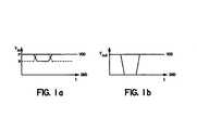
- FIG. 1 ashows a typical differential CMOS signal involving two complementary single-ended signals P, N wherein the highest voltage of the signals is usual referenced to the supply voltage VDD and the differential swing is about a few hundred millivolts.
- a typical CMOS circuitoperates according to one single-ended voltage within a specified voltage range.
- FIG. 1 bshows a typical single-ended logic signal which has a maximum voltage corresponding to logic 1 and a minimum voltage corresponding to logic 0.
- the logic high levelis referenced to the supply voltage VDD and the logic low level is referenced to ground potential.
- the inventive converter stageincludes a first differential stage having a first PMOS transistor and a second PMOS transistor wherein the gate terminal of the first PMOS transistor is coupled to the first single-ended signal of a common mode level differential signal, the gate terminal of the second PMOS transistor is coupled to the second single-ended signal of the common mode level differential signal, and the source terminals of the PMOS transistors are connected to a first current source.
- the inventive converter stagefurther includes a second differential stage having a first NMOS transistor and a second NMOS transistor wherein the gate terminal of the first NMOS transistor is coupled to the first single-ended signal of the differential input signal.
- the gate terminal of the second NMOS transistoris coupled to the second single-ended signal of the differential input signal, and the source terminals of the NMOS transistors are connected to a second current source.
- the drain terminals of the NMOS transistorsare connected to the drain terminals of the PMOS transistors.
- An outputis connected to a node between the drain terminal of the second PMOS transistor and the drain terminal of the second NMOS transistor for providing the single-ended logic output signal having an appropriate minimum and maximum voltage.
- the current sourcesare controlled by the voltage level which is between the mid-potential of the common mode level differential logic signal and the mid-potential of the differential logic input signal.
- the current sourcesare automatically controlled such that both current sources deliver the same constant current to the differential stages.
- the converter stagefurther comprises a complementary output node between the drain terminal of the first PMOS transistor and the connected drain terminal of the first NMOS transistor for providing an inverted single-ended output signal.
- a first pair of resistors in seriesis connected between the gate terminal of the first PMOS transistor and the gate terminal of the second PMOS transistor. Further a second pair of resistors is connected in series between the gate terminal of the first NMOS transistor and the gate terminal of the second NMOS transistor. A node between the resistors of the first pair and a node between the resistors of the second pair advantageously provide the mid-potentials of the common mode level differential logic signal and the differential logic input signal, respectively.
- a third PMOS transistor and a third NMOS transistorare connected in series between the two current sources wherein the source terminal of the PMOS transistor is connected to the first current source and the source terminal of the third NMOS transistor is connected to the second current source.
- the drain terminal of the third PMOS transistoris connected to the drain terminal of the third NMOS transistor, the gate terminal of the third PMOS transistor is connected to the node between the first pair of resistors, and the gate terminal of the third NMOS transistor is connected to the node between the second pair of resistors.
- the voltage level at the node 18 between the two third NMOS and PMOS transistorsis between the mid-potential of the common mode differential logic signal and the mid-potential of the differential logic input signal.
- the first current sourceis a fourth PMOS transistor wherein the source terminal of the fourth PMOS transistors is connected to a supply voltage VDD
- the second current sourceis a fourth NMOS transistor wherein the source terminal of the fourth NMOS transistor is connected to ground potential and the gate terminals of the fourth MOS transistors are connected to the node between the drain terminal of the third PMOS transistor and the drain terminal of the third NMOS transistor.
- the two current sourcesare automatically controlled by the voltage level at the node between the drain of the third PMOS transistor and the drain of the third NMOS transistor, and the current sources deliver both the same constant currents.
- the pairs of resistorsare replaced by pairs of MOS transistors wherein the first pair of resistors is replaced by the source-drain paths of two NMOS transistors being connected in series between the gate terminal of the first PMOS transistor and the gate terminal of the second PMOS transistor.
- the gate terminals of the two pair-NMOS transistorsare connected to a supply voltage.
- the second pair of resistorsis replaced by the source-drain paths of a pair of PMOS transistors connected in series between the gate terminal of the first NMOS transistor and the gate terminal of the second NMOS transistor.
- the gate terminals of the two pair-PMOS transistorsare connected to ground potential.
- the differential logic input signalis a current mode logic signal and the single-ended logic output signal is a CMOS logic signal.
- the first and second PMOS transistorshave the same geometric size and the first and second NMOS transistors have the same geometric size in the circuit.
- the converter stageis preferably operated with differential logic input signals having a clock frequency higher than two gigahertz.
- the converter stageis connected to a means that generates a corresponding common mode differential logic signal from the differential logic input signal.
- FIG. 1 ( a )illustrates a typical differential logic signal.
- FIG. 1 ( b )illustrates a typical single-ended logic signal
- FIG. 2illustrates a differential signal and its corresponding common mode differential signal.
- FIG. 3illustrates an embodiment of a differential logic signal to common mode differential logic signal converter.
- FIG. 4illustrates a preferred embodiment of the inventive converter stage.
- FIG. 5illustrates an alternative embodiment of the converter stage according to the invention.
- FIG. 6illustrates another preferred embodiment of the converter according to the invention.
- the present inventionis a converter stage for converting a differential logic input signal and a corresponding common mode differential logic signal each having a first single-ended logic signal and a complementary second single-ended logic signal into a single-ended logic output signal.
- FIG. 2shows a typical differential current mode logic signal 2 that comprises a first single-ended logic signal 2 - 1 and a complementary second single-ended logic signal 2 - 2 , wherein the mid-potential 20 of the differential signal 2 is centered between the minimum and maximum voltage level of the signal 2 corresponding to the two logic levels.
- the corresponding common mode differential logic signal 5comprises a first and a second single-ended logic signal 5 - 1 , 5 - 2 each having a minimum voltage level and a maximum voltage level and a mid-potential centered in between 19 .
- the minimum voltage levelis usually referenced to ground GND.
- FIG. 2further illustrates a potential 18 which is roughly centered between the two mid-potentials 19 , 20 of the differential logic signal and the corresponding common mode differential logic signal 5 .
- FIG. 3illustrates a common embodiment of a differential logic signal to common mode differential logic signal converter 4 .
- the converter 4comprises a first pair of transistors T 1 , T 2 wherein the respective source-drain paths are connected in series between a supply voltage VDD and ground potential, and wherein the gate terminal of the first transistor T 1 is coupled to the second single-ended logic signal 2 - 2 of the differential logic input signal 2 and the gate terminal of the second transistor T 2 is coupled to the first single-ended logic signal 2 - 1 of the differential logic signal 2 .
- the converter 4comprises a second pair of transistors T 3 , T 4 wherein the respective source-drain paths are connected in series between a supply voltage VDD and ground potential, the gate terminal of the first transistor T 3 of the second pair is connected to the first single-ended logic signal 2 - 1 , and the gate terminal of the second transistor T 4 of the second pair is connected to the second single-ended logic signal 2 - 2 of differential logic input signal 2 .
- the common mode differential logic signal 5comprises two single-ended logic signals 5 - 1 , 5 - 2 , wherein the first single-ended common mode logic signal 5 - 1 is provided on a node N 1 between the source-drain paths of the transistors of the second pair of transistors T 3 , T 4 , and the second single-ended signal 5 - 2 of the common mode level differential signal 5 is provided on a node N 2 which is situated between the source-drain paths of the transistors T 1 , T 2 of the first pair.
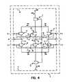
- FIG. 4shows a preferred embodiment of the converter stage according to the invention.
- the converter stageincludes the first differential stage 10 and a second complementary differential stage 11 .
- the first differential stage 10comprises a first PMOS transistor 8 and a second PMOS transistor 9 wherein the gate terminal of the first PMOS transistor 8 is coupled to the first single-ended signal 5 - 1 of the common mode level differential signal 5 , and the gate terminal of the second PMOS transistor 9 is coupled to the second single-ended signal 5 - 2 of the common mode level differential signal 5 .
- the source terminals of the PMOS transistors 8 , 9are connected to a first current source 7 which is realized by transistor.
- the second complementary differential stage 11comprises a first NMOS transistor 13 and a second NMOS transistor 14 wherein the gate terminal of the first NMOS transistor 13 is coupled to the first single-ended signal 2 - 1 of the differential input signal 2 and the gate terminal of the second NMOS transistor 14 is coupled to the second single-ended signal 2 - 2 of the differential signal.
- the source terminals of the NMOS transistors 13 , 14are connected to a second current source 12 which is realized by a transistor.
- the drain terminals of the NMOS transistors 13 , 14 of the second differential stage 11are connected to the drain terminals of the PMOS transistors 8 , 9 of the first differential stage.
- the PMOS transistors 8 , 9 of the first differential stage 10have the same geometric size, and the NMOS transistors 13 , 14 of the second differential stage 11 have the same geometric size.
- a first pair of resistors in series 21 , 22is connected between the gate terminal of the first PMOS transistor 8 and the gate terminal of the second PMOS transistor 9 , hence providing the mid-potential of the common mode differential input signal 5 at a node 19 between the two resistors 21 , 22 of the first pair.
- a second pair resistors 23 , 24 in seriesis connected between the gate terminal of the first NMOS transistor 13 and the gate terminal of the second NMOS transistor 14 , hence providing mid-potential of the differential logic input signal 2 - 1 , 2 - 2 at a node 20 between the two resistors 23 , 24 of the second pair.
- the preferred embodiment of the converter stagefurther comprises a third PMOS transistor 25 and a third NMOS transistor 26 wherein the source terminal of the third PMOS transistor 25 is connected to the first current source 7 — or to the drain terminal of the forth PMOS transistor 7 , respectively.
- the source terminal of the third NMOS transistor 26is connected to the second current source 12 — or to the forth NMOS transistor 12 , respectively.
- the drain terminal of the third PMOS transistor 25is connected to the drain terminal of the third NMOS transistor 26 .
- the gate terminal of the third PMOS transistor 25is connected to the node 19 between the resistors 21 , 22 of the first pair, and the gate terminal of the third NMOS transistor 26 is connected to the node 20 between the resistors 23 , 24 of the second pair.
- the size-ratio between PMOS transistors 8 , 9 of the first differential stage 10 and the NMOS transistors 13 , 14 of the second differential stage 11is the same as the size-ration between the third PMOS transistor 25 and the third NMOS transistor 26 .
- the current sourcesare realized by MOS transistors.
- the first current sourceis a fourth PMOS transistor 7 wherein the source terminal of the fourth PMOS transistor 7 is connected to a supply voltage VDD and the second current source is a fourth NMOS transistor 12 wherein the source terminal of the fourth NMOS transistor is connected to ground potential.
- the drain terminal of the fourth PMOS transistor 7is connected to the source terminals of the first, second and third PMOS transistors 8 , 9 , 19
- the drain terminal of the fourth NMOS transistor 12is connected to the source terminals of the first, second and third NMOS transistors 13 , 14 , 26 .
- the current delivered by the fourth PMOS transistor 7 and the fourth NMOS transistor 12is controlled by the voltage level at the node 18 between the drain of the third PMOS transistor 25 and the drain of the third NMOS transistor 26 because the gate terminals of the fourth MOS transistors 7 , 12 are connected to the node 18 between the third MOS transistors 25 , 26 .
- a single-ended logic output signal 3is provided at a node 17 between the drain terminal of the second PMOS transistor 9 and the drain terminal of the second NMOS transistor 14 .
- a complementary single-ended logic output signal 15is provided at a node 16 between the drain of the first PMOS transistor 8 and the drain terminal of the first NMOS transistor 13 .
- the second outputprovides an inverted output signal 15 .
- the current sources 7 , 12 of the differential stages 10 , 11have to deliver the same amount of constant current I 0 P, I 0 N. This is achieved through the replica path formed by the third PMOS transistor 25 and the third NMOS transistor 26 which are controlled by the mid-potential 19 of the respective differential logic input signal 2 and the mid-potential 20 of the corresponding common mode differential logic signal 5 .
- the complementary second single-ended logic signal 2 - 2 of the differential logic input signal 2is on a logic low level. Then, the current I 2 N through the source-drain path of the second NMOS transistor 14 is zero and the current I 1 N through the source drain path of the first NMOS transistor 13 is the difference between the current I 0 N delivered by the second current source 12 (or the fourth NMOS transistor 12 , respectively) and the current I 3 through the source-drain path of the third NMOS transistor 26 and third PMOS transistor 25 which are included in the replica path.
- the first single-ended logic signal 5 - 1 of the common mode differential logic signal 5 on high logic level and the second single-ended logic signal 5 - 2 of the common mode differential logic signal 5is on logic low level.
- the current I 1 P through the source-drain path of the first PMOS transistor 8is zero
- the current I 2 P through the source-drain path of the second PMOS transistor 9is the difference between the current I 0 P delivered by the first current source 7 (or the fourth PMOS transistor 7 , respectively) and the current I 3 through the source-drain path of the third PMOS transistor 25 and the third NMOS transistor 26 in the replica path.
- the voltage level at the output node 17increases and the voltage level at the second complementary output node 16 decreases.
- the MOS transistors in the differential stages 10 , 11are chosen such that a current through a switched off source-drain path is zero for a swing of the differential signals, i.e. the difference between maximum voltage level and minimum voltage level corresponding to logic high and logic low level.
- the resistors 21 , 22 , 23 , 24should have all the same resistances and are preferably of about 20 kiloohm but they can have other resistances.
- the voltage level between the third PMOS transistor 25 and the third NMOS transistor 26 in the replica pathis roughly centered between the mid-potentials 19 , 20 of the differential logic input signal 2 and the corresponding common mode differential logic signal 5 .
- This generated voltage level 18is used as a bias potential for the two current-source MOS transistors 7 , 12 , such that they automatically deliver the same amount of current I 0 P, I 0 N. Doing so, the switching point of the single-ended output signals 3 , 15 is exactly centered between the voltage level corresponding to logic high and the voltage level corresponding to logic low.
- inverter stagesare coupled to the single-ended output signals 3 , 15 .
- the inverter stagesrise the maximum voltage level of the single-ended output signal 3 , 15 to a preferred maximum voltage level corresponding to a high logic level, for example the supply voltage VDD.
- the inverter stagesdecrease the minimum voltage level of the single-ended output signals 3 , 15 to a preferred minimum voltage level corresponding to a logic low level, for example ground potential.
- An advantage of the preferred embodiment of the inventionis that it has a very high switching velocity due to the small amount of switching devices. Another advantage is that the automatic control of the current sources 7 , 12 is realized through a replica path formed by the source-drain paths of the third MOS transistors 25 , 26 . Therefore, the control does not influence the input and output signals. Yet another advantage of the preferred embodiment is that the rising edges and the falling edges of the single-ended output signals are generated symmetrically and by the same devices in the circuit. Further, the generation of the mid-potentials of the differential logic input signal and the corresponding common mode differential logic signal 5 is very robust against nonlinearities in the input signals. It is a further advantage of the inventive converter stage 6 that the inverted single-ended output signal 15 is provided without any delay with respect to the noninverted single-ended logic output signal 3 .
- FIG. 5shows an alternative embodiment of the converter stage 6 according to the invention wherein the resistors 21 , 22 , 23 , 24 are replaced by the source-drain paths of MOS transistors 27 , 28 , 29 , 30 .
- the resistances of the respective source-drain pathsare employed as resistors while the gate terminals of NMOS transistors 27 , 28 are connected to the supply voltage VDD, and the gate terminals of PMOS transistors 29 , 30 are connected to ground potential.
- the transistorsare chosen and operated in their linear regime.
- the converter stage 6is connected to a means 4 that generates the corresponding common mode differential logic signal 5 from the differential logic input signal 2 .
- the second preferred embodimentis shown in FIG. 6 .
- the converter 1 according to the second preferred embodiment of the invention for converting a differential logic input signal 2 having a first single-ended logic signal 2 - 1 and a second single-ended logic signal 2 - 2 into a single-ended logic output signal 3comprises a means 4 for generating a common mode differential logic signal 5 having a first single ended logic signal 5 - 1 and a complementary second single-ended logic signal 5 - 2 .
- the second preferred embodimentfurther comprises a converter stage 6 according to the invention that is coupled to the differential logic input signal 2 and coupled to the means 4 for receiving the corresponding common mode differential logic signal 5 .
- the means 4 and the converter stage 6are realized in the same integrated circuit.
Landscapes
- Physics & Mathematics (AREA)
- Nonlinear Science (AREA)
- Engineering & Computer Science (AREA)
- Computer Hardware Design (AREA)
- Computing Systems (AREA)
- General Engineering & Computer Science (AREA)
- Mathematical Physics (AREA)
- Logic Circuits (AREA)
Abstract
Description
Claims (16)
Priority Applications (1)
| Application Number | Priority Date | Filing Date | Title |
|---|---|---|---|
| US10/672,393US6924668B2 (en) | 2003-09-25 | 2003-09-25 | Differential to single-ended logic converter |
Applications Claiming Priority (1)
| Application Number | Priority Date | Filing Date | Title |
|---|---|---|---|
| US10/672,393US6924668B2 (en) | 2003-09-25 | 2003-09-25 | Differential to single-ended logic converter |
Publications (2)
| Publication Number | Publication Date |
|---|---|
| US20050068063A1 US20050068063A1 (en) | 2005-03-31 |
| US6924668B2true US6924668B2 (en) | 2005-08-02 |
Family
ID=34376346
Family Applications (1)
| Application Number | Title | Priority Date | Filing Date |
|---|---|---|---|
| US10/672,393Expired - Fee RelatedUS6924668B2 (en) | 2003-09-25 | 2003-09-25 | Differential to single-ended logic converter |
Country Status (1)
| Country | Link |
|---|---|
| US (1) | US6924668B2 (en) |
Cited By (41)
| Publication number | Priority date | Publication date | Assignee | Title |
|---|---|---|---|---|
| US20060012429A1 (en)* | 2004-07-09 | 2006-01-19 | Samsung Electronics Co., Ltd. | Self biased differential amplifier |
| US20070252618A1 (en)* | 2006-04-28 | 2007-11-01 | Karthik Gopalakrishnan | Signal converter circuit |
| US7737724B2 (en) | 2007-04-17 | 2010-06-15 | Cypress Semiconductor Corporation | Universal digital block interconnection and channel routing |
| US20100164539A1 (en)* | 2008-12-31 | 2010-07-01 | Ganesh Balamurugan | System and apparatus of reconfigurable transceiver design for multi-mode signaling |
| US7761845B1 (en) | 2002-09-09 | 2010-07-20 | Cypress Semiconductor Corporation | Method for parameterizing a user module |
| US7765095B1 (en) | 2000-10-26 | 2010-07-27 | Cypress Semiconductor Corporation | Conditional branching in an in-circuit emulation system |
| US7770113B1 (en) | 2001-11-19 | 2010-08-03 | Cypress Semiconductor Corporation | System and method for dynamically generating a configuration datasheet |
| US7774190B1 (en) | 2001-11-19 | 2010-08-10 | Cypress Semiconductor Corporation | Sleep and stall in an in-circuit emulation system |
| US7825688B1 (en) | 2000-10-26 | 2010-11-02 | Cypress Semiconductor Corporation | Programmable microcontroller architecture(mixed analog/digital) |
| US7844437B1 (en) | 2001-11-19 | 2010-11-30 | Cypress Semiconductor Corporation | System and method for performing next placements and pruning of disallowed placements for programming an integrated circuit |
| US7893724B2 (en) | 2004-03-25 | 2011-02-22 | Cypress Semiconductor Corporation | Method and circuit for rapid alignment of signals |
| US8026739B2 (en) | 2007-04-17 | 2011-09-27 | Cypress Semiconductor Corporation | System level interconnect with programmable switching |
| US8049569B1 (en) | 2007-09-05 | 2011-11-01 | Cypress Semiconductor Corporation | Circuit and method for improving the accuracy of a crystal-less oscillator having dual-frequency modes |
| US8067948B2 (en) | 2006-03-27 | 2011-11-29 | Cypress Semiconductor Corporation | Input/output multiplexer bus |
| US8069436B2 (en) | 2004-08-13 | 2011-11-29 | Cypress Semiconductor Corporation | Providing hardware independence to automate code generation of processing device firmware |
| US8069428B1 (en) | 2001-10-24 | 2011-11-29 | Cypress Semiconductor Corporation | Techniques for generating microcontroller configuration information |
| US8069405B1 (en) | 2001-11-19 | 2011-11-29 | Cypress Semiconductor Corporation | User interface for efficiently browsing an electronic document using data-driven tabs |
| US8078894B1 (en) | 2007-04-25 | 2011-12-13 | Cypress Semiconductor Corporation | Power management architecture, method and configuration system |
| US8078970B1 (en) | 2001-11-09 | 2011-12-13 | Cypress Semiconductor Corporation | Graphical user interface with user-selectable list-box |
| US8085100B2 (en) | 2005-02-04 | 2011-12-27 | Cypress Semiconductor Corporation | Poly-phase frequency synthesis oscillator |
| US8085067B1 (en) | 2005-12-21 | 2011-12-27 | Cypress Semiconductor Corporation | Differential-to-single ended signal converter circuit and method |
| US8089461B2 (en) | 2005-06-23 | 2012-01-03 | Cypress Semiconductor Corporation | Touch wake for electronic devices |
| US8092083B2 (en) | 2007-04-17 | 2012-01-10 | Cypress Semiconductor Corporation | Temperature sensor with digital bandgap |
| US8103496B1 (en) | 2000-10-26 | 2012-01-24 | Cypress Semicondutor Corporation | Breakpoint control in an in-circuit emulation system |
| US8103497B1 (en) | 2002-03-28 | 2012-01-24 | Cypress Semiconductor Corporation | External interface for event architecture |
| US8120408B1 (en) | 2005-05-05 | 2012-02-21 | Cypress Semiconductor Corporation | Voltage controlled oscillator delay cell and method |
| US8130025B2 (en) | 2007-04-17 | 2012-03-06 | Cypress Semiconductor Corporation | Numerical band gap |
| US8149048B1 (en) | 2000-10-26 | 2012-04-03 | Cypress Semiconductor Corporation | Apparatus and method for programmable power management in a programmable analog circuit block |
| US8160864B1 (en) | 2000-10-26 | 2012-04-17 | Cypress Semiconductor Corporation | In-circuit emulator and pod synchronized boot |
| US8176296B2 (en) | 2000-10-26 | 2012-05-08 | Cypress Semiconductor Corporation | Programmable microcontroller architecture |
| US8286125B2 (en) | 2004-08-13 | 2012-10-09 | Cypress Semiconductor Corporation | Model for a hardware device-independent method of defining embedded firmware for programmable systems |
| US8402313B1 (en) | 2002-05-01 | 2013-03-19 | Cypress Semiconductor Corporation | Reconfigurable testing system and method |
| US8499270B1 (en) | 2007-04-25 | 2013-07-30 | Cypress Semiconductor Corporation | Configuration of programmable IC design elements |
| US8516025B2 (en) | 2007-04-17 | 2013-08-20 | Cypress Semiconductor Corporation | Clock driven dynamic datapath chaining |
| US8533677B1 (en) | 2001-11-19 | 2013-09-10 | Cypress Semiconductor Corporation | Graphical user interface for dynamically reconfiguring a programmable device |
| RU2580799C1 (en)* | 2015-03-17 | 2016-04-10 | Федеральное государственное бюджетное образовательное учреждение высшего профессионального образования "Ульяновский государственный технический университет" | Logic transducer |
| US9448964B2 (en) | 2009-05-04 | 2016-09-20 | Cypress Semiconductor Corporation | Autonomous control in a programmable system |
| US9564902B2 (en) | 2007-04-17 | 2017-02-07 | Cypress Semiconductor Corporation | Dynamically configurable and re-configurable data path |
| US9720805B1 (en) | 2007-04-25 | 2017-08-01 | Cypress Semiconductor Corporation | System and method for controlling a target device |
| US10256998B1 (en)* | 2018-05-03 | 2019-04-09 | Micron Technology, Inc. | Reducing supply noise in current mode logic transmitters |
| US10698662B2 (en) | 2001-11-15 | 2020-06-30 | Cypress Semiconductor Corporation | System providing automatic source code generation for personalization and parameterization of user modules |
Families Citing this family (2)
| Publication number | Priority date | Publication date | Assignee | Title |
|---|---|---|---|---|
| US7821300B2 (en)* | 2008-12-03 | 2010-10-26 | International Business Machines Corporation | System and method for converting between CML signal logic families |
| CN109842416B (en)* | 2018-12-31 | 2024-02-23 | 芯动微电子科技(珠海)有限公司 | Transmitting apparatus |
Citations (5)
| Publication number | Priority date | Publication date | Assignee | Title |
|---|---|---|---|---|
| US5714906A (en)* | 1995-08-14 | 1998-02-03 | Motamed; Ali | Constant transductance input stage and integrated circuit implementations thereof |
| US5953276A (en)* | 1997-12-18 | 1999-09-14 | Micron Technology, Inc. | Fully-differential amplifier |
| US6111431A (en)* | 1998-05-14 | 2000-08-29 | National Semiconductor Corporation | LVDS driver for backplane applications |
| US6452429B1 (en)* | 1999-05-19 | 2002-09-17 | Samsung Electronics Co., Ltd. | High speed input buffer circuit for low voltage interface |
| US6686772B2 (en)* | 2001-11-19 | 2004-02-03 | Broadcom Corporation | Voltage mode differential driver and method |
- 2003
- 2003-09-25USUS10/672,393patent/US6924668B2/ennot_activeExpired - Fee Related
Patent Citations (5)
| Publication number | Priority date | Publication date | Assignee | Title |
|---|---|---|---|---|
| US5714906A (en)* | 1995-08-14 | 1998-02-03 | Motamed; Ali | Constant transductance input stage and integrated circuit implementations thereof |
| US5953276A (en)* | 1997-12-18 | 1999-09-14 | Micron Technology, Inc. | Fully-differential amplifier |
| US6111431A (en)* | 1998-05-14 | 2000-08-29 | National Semiconductor Corporation | LVDS driver for backplane applications |
| US6452429B1 (en)* | 1999-05-19 | 2002-09-17 | Samsung Electronics Co., Ltd. | High speed input buffer circuit for low voltage interface |
| US6686772B2 (en)* | 2001-11-19 | 2004-02-03 | Broadcom Corporation | Voltage mode differential driver and method |
Cited By (59)
| Publication number | Priority date | Publication date | Assignee | Title |
|---|---|---|---|---|
| US8103496B1 (en) | 2000-10-26 | 2012-01-24 | Cypress Semicondutor Corporation | Breakpoint control in an in-circuit emulation system |
| US10725954B2 (en) | 2000-10-26 | 2020-07-28 | Monterey Research, Llc | Microcontroller programmable system on a chip |
| US10261932B2 (en) | 2000-10-26 | 2019-04-16 | Cypress Semiconductor Corporation | Microcontroller programmable system on a chip |
| US10248604B2 (en) | 2000-10-26 | 2019-04-02 | Cypress Semiconductor Corporation | Microcontroller programmable system on a chip |
| US10020810B2 (en) | 2000-10-26 | 2018-07-10 | Cypress Semiconductor Corporation | PSoC architecture |
| US7765095B1 (en) | 2000-10-26 | 2010-07-27 | Cypress Semiconductor Corporation | Conditional branching in an in-circuit emulation system |
| US9843327B1 (en) | 2000-10-26 | 2017-12-12 | Cypress Semiconductor Corporation | PSOC architecture |
| US9766650B2 (en) | 2000-10-26 | 2017-09-19 | Cypress Semiconductor Corporation | Microcontroller programmable system on a chip with programmable interconnect |
| US7825688B1 (en) | 2000-10-26 | 2010-11-02 | Cypress Semiconductor Corporation | Programmable microcontroller architecture(mixed analog/digital) |
| US8736303B2 (en) | 2000-10-26 | 2014-05-27 | Cypress Semiconductor Corporation | PSOC architecture |
| US8555032B2 (en) | 2000-10-26 | 2013-10-08 | Cypress Semiconductor Corporation | Microcontroller programmable system on a chip with programmable interconnect |
| US8358150B1 (en) | 2000-10-26 | 2013-01-22 | Cypress Semiconductor Corporation | Programmable microcontroller architecture(mixed analog/digital) |
| US8176296B2 (en) | 2000-10-26 | 2012-05-08 | Cypress Semiconductor Corporation | Programmable microcontroller architecture |
| US8160864B1 (en) | 2000-10-26 | 2012-04-17 | Cypress Semiconductor Corporation | In-circuit emulator and pod synchronized boot |
| US8149048B1 (en) | 2000-10-26 | 2012-04-03 | Cypress Semiconductor Corporation | Apparatus and method for programmable power management in a programmable analog circuit block |
| US8793635B1 (en) | 2001-10-24 | 2014-07-29 | Cypress Semiconductor Corporation | Techniques for generating microcontroller configuration information |
| US10466980B2 (en) | 2001-10-24 | 2019-11-05 | Cypress Semiconductor Corporation | Techniques for generating microcontroller configuration information |
| US8069428B1 (en) | 2001-10-24 | 2011-11-29 | Cypress Semiconductor Corporation | Techniques for generating microcontroller configuration information |
| US8078970B1 (en) | 2001-11-09 | 2011-12-13 | Cypress Semiconductor Corporation | Graphical user interface with user-selectable list-box |
| US10698662B2 (en) | 2001-11-15 | 2020-06-30 | Cypress Semiconductor Corporation | System providing automatic source code generation for personalization and parameterization of user modules |
| US7844437B1 (en) | 2001-11-19 | 2010-11-30 | Cypress Semiconductor Corporation | System and method for performing next placements and pruning of disallowed placements for programming an integrated circuit |
| US8533677B1 (en) | 2001-11-19 | 2013-09-10 | Cypress Semiconductor Corporation | Graphical user interface for dynamically reconfiguring a programmable device |
| US7774190B1 (en) | 2001-11-19 | 2010-08-10 | Cypress Semiconductor Corporation | Sleep and stall in an in-circuit emulation system |
| US8370791B2 (en) | 2001-11-19 | 2013-02-05 | Cypress Semiconductor Corporation | System and method for performing next placements and pruning of disallowed placements for programming an integrated circuit |
| US8069405B1 (en) | 2001-11-19 | 2011-11-29 | Cypress Semiconductor Corporation | User interface for efficiently browsing an electronic document using data-driven tabs |
| US7770113B1 (en) | 2001-11-19 | 2010-08-03 | Cypress Semiconductor Corporation | System and method for dynamically generating a configuration datasheet |
| US8103497B1 (en) | 2002-03-28 | 2012-01-24 | Cypress Semiconductor Corporation | External interface for event architecture |
| US8402313B1 (en) | 2002-05-01 | 2013-03-19 | Cypress Semiconductor Corporation | Reconfigurable testing system and method |
| US7761845B1 (en) | 2002-09-09 | 2010-07-20 | Cypress Semiconductor Corporation | Method for parameterizing a user module |
| US7893724B2 (en) | 2004-03-25 | 2011-02-22 | Cypress Semiconductor Corporation | Method and circuit for rapid alignment of signals |
| US20060012429A1 (en)* | 2004-07-09 | 2006-01-19 | Samsung Electronics Co., Ltd. | Self biased differential amplifier |
| US8069436B2 (en) | 2004-08-13 | 2011-11-29 | Cypress Semiconductor Corporation | Providing hardware independence to automate code generation of processing device firmware |
| US8286125B2 (en) | 2004-08-13 | 2012-10-09 | Cypress Semiconductor Corporation | Model for a hardware device-independent method of defining embedded firmware for programmable systems |
| US8085100B2 (en) | 2005-02-04 | 2011-12-27 | Cypress Semiconductor Corporation | Poly-phase frequency synthesis oscillator |
| US8120408B1 (en) | 2005-05-05 | 2012-02-21 | Cypress Semiconductor Corporation | Voltage controlled oscillator delay cell and method |
| US8089461B2 (en) | 2005-06-23 | 2012-01-03 | Cypress Semiconductor Corporation | Touch wake for electronic devices |
| US8085067B1 (en) | 2005-12-21 | 2011-12-27 | Cypress Semiconductor Corporation | Differential-to-single ended signal converter circuit and method |
| US8067948B2 (en) | 2006-03-27 | 2011-11-29 | Cypress Semiconductor Corporation | Input/output multiplexer bus |
| US8717042B1 (en) | 2006-03-27 | 2014-05-06 | Cypress Semiconductor Corporation | Input/output multiplexer bus |
| US20070252618A1 (en)* | 2006-04-28 | 2007-11-01 | Karthik Gopalakrishnan | Signal converter circuit |
| US9564902B2 (en) | 2007-04-17 | 2017-02-07 | Cypress Semiconductor Corporation | Dynamically configurable and re-configurable data path |
| US7737724B2 (en) | 2007-04-17 | 2010-06-15 | Cypress Semiconductor Corporation | Universal digital block interconnection and channel routing |
| US8092083B2 (en) | 2007-04-17 | 2012-01-10 | Cypress Semiconductor Corporation | Temperature sensor with digital bandgap |
| US8130025B2 (en) | 2007-04-17 | 2012-03-06 | Cypress Semiconductor Corporation | Numerical band gap |
| US8516025B2 (en) | 2007-04-17 | 2013-08-20 | Cypress Semiconductor Corporation | Clock driven dynamic datapath chaining |
| US8026739B2 (en) | 2007-04-17 | 2011-09-27 | Cypress Semiconductor Corporation | System level interconnect with programmable switching |
| US8476928B1 (en) | 2007-04-17 | 2013-07-02 | Cypress Semiconductor Corporation | System level interconnect with programmable switching |
| US9720805B1 (en) | 2007-04-25 | 2017-08-01 | Cypress Semiconductor Corporation | System and method for controlling a target device |
| US8909960B1 (en) | 2007-04-25 | 2014-12-09 | Cypress Semiconductor Corporation | Power management architecture, method and configuration system |
| US8499270B1 (en) | 2007-04-25 | 2013-07-30 | Cypress Semiconductor Corporation | Configuration of programmable IC design elements |
| US8078894B1 (en) | 2007-04-25 | 2011-12-13 | Cypress Semiconductor Corporation | Power management architecture, method and configuration system |
| US8049569B1 (en) | 2007-09-05 | 2011-11-01 | Cypress Semiconductor Corporation | Circuit and method for improving the accuracy of a crystal-less oscillator having dual-frequency modes |
| US7919984B2 (en)* | 2008-12-31 | 2011-04-05 | Intel Corporation | System and apparatus of reconfigurable transceiver design for multi-mode signaling |
| US20100164539A1 (en)* | 2008-12-31 | 2010-07-01 | Ganesh Balamurugan | System and apparatus of reconfigurable transceiver design for multi-mode signaling |
| US9448964B2 (en) | 2009-05-04 | 2016-09-20 | Cypress Semiconductor Corporation | Autonomous control in a programmable system |
| RU2580799C1 (en)* | 2015-03-17 | 2016-04-10 | Федеральное государственное бюджетное образовательное учреждение высшего профессионального образования "Ульяновский государственный технический университет" | Logic transducer |
| US10256998B1 (en)* | 2018-05-03 | 2019-04-09 | Micron Technology, Inc. | Reducing supply noise in current mode logic transmitters |
| US10277426B1 (en)* | 2018-05-03 | 2019-04-30 | Micron Technology, Inc. | Reducing supply noise in current mode logic transmitters |
| US10411916B1 (en)* | 2018-05-03 | 2019-09-10 | Micron Technology, Inc. | Reducing supply noise in current mode logic transmitters |
Also Published As
| Publication number | Publication date |
|---|---|
| US20050068063A1 (en) | 2005-03-31 |
Similar Documents
| Publication | Publication Date | Title |
|---|---|---|
| US6924668B2 (en) | Differential to single-ended logic converter | |
| US4779016A (en) | Level conversion circuit | |
| US8063808B2 (en) | Multi-input operational amplifier circuit, digital/analog converter using same, and driver for display device using same | |
| EP0935345A2 (en) | Differential switching circuitry | |
| US6791391B2 (en) | Level shifting circuit | |
| US5214317A (en) | CMOS to ECL translator with incorporated latch | |
| EP0232969A1 (en) | Level conversion circuit | |
| US7265622B1 (en) | Differential difference amplifier | |
| IE903199A1 (en) | Signal level converter | |
| KR930004351B1 (en) | Level shift circuit | |
| JP2008544714A (en) | Differential transistor vs. current switch supplied with low voltage VCC | |
| US6211699B1 (en) | High performance CML to CMOS converter | |
| CN116073801B (en) | Phase interpolator and phase buffer circuits | |
| US11967395B2 (en) | Buffers and multiplexers | |
| US7088142B2 (en) | Semiconductor integrated circuit and level conversion circuit | |
| JPH10336010A (en) | Cmlcmos conversion circuit | |
| US10917095B2 (en) | Level shifting circuit and integrated circuit | |
| US7847591B2 (en) | Low jitter CMOS to CML converter | |
| EP0875996B1 (en) | Logic device | |
| US6781420B2 (en) | Symmetric differential logic circuits | |
| US6646486B2 (en) | Semiconductor integrated circuit | |
| US20080238517A1 (en) | Oscillator Circuit and Semiconductor Device | |
| US7132857B2 (en) | High speed receiver with wide input voltage range | |
| US20080150584A1 (en) | Cml circuit | |
| US6329866B1 (en) | Transient current producing method, transient current producing circuit, related semiconductor integrated circuit and logical circuit |
Legal Events
| Date | Code | Title | Description |
|---|---|---|---|
| AS | Assignment | Owner name:INFINEON TECHNOLOGIES, AG, GERMANY Free format text:ASSIGNMENT OF ASSIGNORS INTEREST;ASSIGNORS:MULLER, DAVID;REBMANN, VOLKMAR;REEL/FRAME:014844/0760 Effective date:20031027 | |
| FEPP | Fee payment procedure | Free format text:PAYOR NUMBER ASSIGNED (ORIGINAL EVENT CODE: ASPN); ENTITY STATUS OF PATENT OWNER: LARGE ENTITY | |
| FPAY | Fee payment | Year of fee payment:4 | |
| FEPP | Fee payment procedure | Free format text:PAYER NUMBER DE-ASSIGNED (ORIGINAL EVENT CODE: RMPN); ENTITY STATUS OF PATENT OWNER: LARGE ENTITY Free format text:PAYOR NUMBER ASSIGNED (ORIGINAL EVENT CODE: ASPN); ENTITY STATUS OF PATENT OWNER: LARGE ENTITY | |
| AS | Assignment | Owner name:ELPIDA MEMORY, INC., JAPAN Free format text:ASSIGNMENT OF ASSIGNORS INTEREST;ASSIGNOR:INFINEON TECHNOLOGIES;REEL/FRAME:024698/0224 Effective date:20100601 | |
| FPAY | Fee payment | Year of fee payment:8 | |
| AS | Assignment | Owner name:ELPIDA MEMORY INC., JAPAN Free format text:SECURITY AGREEMENT;ASSIGNOR:PS4 LUXCO S.A.R.L.;REEL/FRAME:032414/0261 Effective date:20130726 | |
| AS | Assignment | Owner name:PS4 LUXCO S.A.R.L., LUXEMBOURG Free format text:ASSIGNMENT OF ASSIGNORS INTEREST;ASSIGNOR:ELPIDA MEMORY, INC.;REEL/FRAME:032899/0588 Effective date:20130726 | |
| AS | Assignment | Owner name:PS5 LUXCO S.A.R.L., LUXEMBOURG Free format text:ASSIGNMENT OF ASSIGNORS INTEREST;ASSIGNOR:PS4 LUXCO S.A.R.L.;REEL/FRAME:039818/0506 Effective date:20130829 Owner name:LONGITUDE SEMICONDUCTOR S.A.R.L., LUXEMBOURG Free format text:CHANGE OF NAME;ASSIGNOR:PS5 LUXCO S.A.R.L.;REEL/FRAME:039793/0880 Effective date:20131112 | |
| REMI | Maintenance fee reminder mailed | ||
| LAPS | Lapse for failure to pay maintenance fees | Free format text:PATENT EXPIRED FOR FAILURE TO PAY MAINTENANCE FEES (ORIGINAL EVENT CODE: EXP.) | |
| STCH | Information on status: patent discontinuation | Free format text:PATENT EXPIRED DUE TO NONPAYMENT OF MAINTENANCE FEES UNDER 37 CFR 1.362 | |
| FP | Lapsed due to failure to pay maintenance fee | Effective date:20170802 |