US6924538B2 - Devices having vertically-disposed nanofabric articles and methods of making the same - Google Patents
Devices having vertically-disposed nanofabric articles and methods of making the sameDownload PDFInfo
- Publication number
- US6924538B2 US6924538B2US10/776,572US77657204AUS6924538B2US 6924538 B2US6924538 B2US 6924538B2US 77657204 AUS77657204 AUS 77657204AUS 6924538 B2US6924538 B2US 6924538B2
- Authority
- US
- United States
- Prior art keywords
- conductive trace
- nanotube article
- electro
- channel
- article
- Prior art date
- Legal status (The legal status is an assumption and is not a legal conclusion. Google has not performed a legal analysis and makes no representation as to the accuracy of the status listed.)
- Expired - Fee Related
Links
- 239000002059nanofabricSubstances0.000titleclaimsabstractdescription121
- 238000000034methodMethods0.000titleclaimsabstractdescription37
- 239000002071nanotubeSubstances0.000claimsabstractdescription80
- 239000010409thin filmSubstances0.000claimsabstractdescription8
- 239000004020conductorSubstances0.000claimsabstractdescription6
- 230000008569processEffects0.000claimsabstractdescription3
- 239000011248coating agentSubstances0.000claimsdescription3
- 238000000576coating methodMethods0.000claimsdescription3
- 230000015654memoryEffects0.000abstractdescription28
- 238000010276constructionMethods0.000abstractdescription5
- 239000010410layerSubstances0.000description73
- 239000004744fabricSubstances0.000description13
- 238000004519manufacturing processMethods0.000description13
- 239000000463materialSubstances0.000description13
- 229910021420polycrystalline siliconInorganic materials0.000description10
- 229920005591polysiliconPolymers0.000description10
- 238000005516engineering processMethods0.000description8
- 239000000758substrateSubstances0.000description8
- VYPSYNLAJGMNEJ-UHFFFAOYSA-NSilicium dioxideChemical compoundO=[Si]=OVYPSYNLAJGMNEJ-UHFFFAOYSA-N0.000description7
- 229910052751metalInorganic materials0.000description7
- 239000002184metalSubstances0.000description7
- 239000004065semiconductorSubstances0.000description7
- 230000003993interactionEffects0.000description6
- 238000005530etchingMethods0.000description5
- 238000001465metallisationMethods0.000description5
- 238000000151depositionMethods0.000description4
- 239000011159matrix materialSubstances0.000description4
- 230000001681protective effectEffects0.000description4
- 238000001039wet etchingMethods0.000description4
- OKTJSMMVPCPJKN-UHFFFAOYSA-NCarbonChemical compound[C]OKTJSMMVPCPJKN-UHFFFAOYSA-N0.000description3
- 229910052581Si3N4Inorganic materials0.000description3
- 230000006399behaviorEffects0.000description3
- 230000008901benefitEffects0.000description3
- 239000002131composite materialSubstances0.000description3
- 230000003247decreasing effectEffects0.000description3
- 239000010408filmSubstances0.000description3
- 150000002739metalsChemical class0.000description3
- HQVNEWCFYHHQES-UHFFFAOYSA-Nsilicon nitrideChemical compoundN12[Si]34N5[Si]62N3[Si]51N64HQVNEWCFYHHQES-UHFFFAOYSA-N0.000description3
- 229910052814silicon oxideInorganic materials0.000description3
- 239000002109single walled nanotubeSubstances0.000description3
- 238000013459approachMethods0.000description2
- 238000003491arrayMethods0.000description2
- 239000002041carbon nanotubeSubstances0.000description2
- 229910021393carbon nanotubeInorganic materials0.000description2
- 230000001419dependent effectEffects0.000description2
- 230000008021depositionEffects0.000description2
- 238000010586diagramMethods0.000description2
- 230000003292diminished effectEffects0.000description2
- 230000000694effectsEffects0.000description2
- 239000007772electrode materialSubstances0.000description2
- 239000000835fiberSubstances0.000description2
- 239000011810insulating materialSubstances0.000description2
- 238000009413insulationMethods0.000description2
- 239000012212insulatorSubstances0.000description2
- 238000001000micrographMethods0.000description2
- 239000004745nonwoven fabricSubstances0.000description2
- 229910052710siliconInorganic materials0.000description2
- 239000010703siliconSubstances0.000description2
- 235000012239silicon dioxideNutrition0.000description2
- 239000000377silicon dioxideSubstances0.000description2
- 239000002356single layerSubstances0.000description2
- 238000003860storageMethods0.000description2
- 239000000126substanceSubstances0.000description2
- 239000000725suspensionSubstances0.000description2
- 238000000427thin-film depositionMethods0.000description2
- RTAQQCXQSZGOHL-UHFFFAOYSA-NTitaniumChemical compound[Ti]RTAQQCXQSZGOHL-UHFFFAOYSA-N0.000description1
- 238000005411Van der Waals forceMethods0.000description1
- 230000004913activationEffects0.000description1
- 238000004873anchoringMethods0.000description1
- 230000015572biosynthetic processEffects0.000description1
- 229910052799carbonInorganic materials0.000description1
- 150000001722carbon compoundsChemical class0.000description1
- 239000002238carbon nanotube filmSubstances0.000description1
- 230000001413cellular effectEffects0.000description1
- 230000008859changeEffects0.000description1
- 238000005229chemical vapour depositionMethods0.000description1
- 230000001351cycling effectEffects0.000description1
- 230000001066destructive effectEffects0.000description1
- 230000003467diminishing effectEffects0.000description1
- 238000007598dipping methodMethods0.000description1
- 238000009826distributionMethods0.000description1
- 238000001312dry etchingMethods0.000description1
- 238000007306functionalization reactionMethods0.000description1
- 239000011521glassSubstances0.000description1
- 238000003384imaging methodMethods0.000description1
- 230000006872improvementEffects0.000description1
- 230000010354integrationEffects0.000description1
- 150000002500ionsChemical class0.000description1
- 238000001459lithographyMethods0.000description1
- 230000004048modificationEffects0.000description1
- 238000012986modificationMethods0.000description1
- 239000002086nanomaterialSubstances0.000description1
- 238000004806packaging method and processMethods0.000description1
- 230000000704physical effectEffects0.000description1
- 238000001020plasma etchingMethods0.000description1
- 238000007781pre-processingMethods0.000description1
- 102000004169proteins and genesHuman genes0.000description1
- 108090000623proteins and genesProteins0.000description1
- 150000003220pyrenesChemical class0.000description1
- 230000009467reductionEffects0.000description1
- 230000026280response to electrical stimulusEffects0.000description1
- 238000001338self-assemblyMethods0.000description1
- 238000000926separation methodMethods0.000description1
- 125000006850spacer groupChemical group0.000description1
- 238000004528spin coatingMethods0.000description1
- 238000004544sputter depositionMethods0.000description1
- 229910052719titaniumInorganic materials0.000description1
- 239000010936titaniumSubstances0.000description1
- 230000001052transient effectEffects0.000description1
- 230000007704transitionEffects0.000description1
Images


Classifications
- G—PHYSICS
- G11—INFORMATION STORAGE
- G11C—STATIC STORES
- G11C13/00—Digital stores characterised by the use of storage elements not covered by groups G11C11/00, G11C23/00, or G11C25/00
- G11C13/02—Digital stores characterised by the use of storage elements not covered by groups G11C11/00, G11C23/00, or G11C25/00 using elements whose operation depends upon chemical change
- G11C13/025—Digital stores characterised by the use of storage elements not covered by groups G11C11/00, G11C23/00, or G11C25/00 using elements whose operation depends upon chemical change using fullerenes, e.g. C60, or nanotubes, e.g. carbon or silicon nanotubes
- B—PERFORMING OPERATIONS; TRANSPORTING
- B81—MICROSTRUCTURAL TECHNOLOGY
- B81C—PROCESSES OR APPARATUS SPECIALLY ADAPTED FOR THE MANUFACTURE OR TREATMENT OF MICROSTRUCTURAL DEVICES OR SYSTEMS
- B81C1/00—Manufacture or treatment of devices or systems in or on a substrate
- B81C1/00015—Manufacture or treatment of devices or systems in or on a substrate for manufacturing microsystems
- B81C1/00134—Manufacture or treatment of devices or systems in or on a substrate for manufacturing microsystems comprising flexible or deformable structures
- B81C1/00142—Bridges
- B—PERFORMING OPERATIONS; TRANSPORTING
- B82—NANOTECHNOLOGY
- B82Y—SPECIFIC USES OR APPLICATIONS OF NANOSTRUCTURES; MEASUREMENT OR ANALYSIS OF NANOSTRUCTURES; MANUFACTURE OR TREATMENT OF NANOSTRUCTURES
- B82Y10/00—Nanotechnology for information processing, storage or transmission, e.g. quantum computing or single electron logic
- B—PERFORMING OPERATIONS; TRANSPORTING
- B82—NANOTECHNOLOGY
- B82Y—SPECIFIC USES OR APPLICATIONS OF NANOSTRUCTURES; MEASUREMENT OR ANALYSIS OF NANOSTRUCTURES; MANUFACTURE OR TREATMENT OF NANOSTRUCTURES
- B82Y30/00—Nanotechnology for materials or surface science, e.g. nanocomposites
- B—PERFORMING OPERATIONS; TRANSPORTING
- B82—NANOTECHNOLOGY
- B82Y—SPECIFIC USES OR APPLICATIONS OF NANOSTRUCTURES; MEASUREMENT OR ANALYSIS OF NANOSTRUCTURES; MANUFACTURE OR TREATMENT OF NANOSTRUCTURES
- B82Y40/00—Manufacture or treatment of nanostructures
- C—CHEMISTRY; METALLURGY
- C01—INORGANIC CHEMISTRY
- C01B—NON-METALLIC ELEMENTS; COMPOUNDS THEREOF; METALLOIDS OR COMPOUNDS THEREOF NOT COVERED BY SUBCLASS C01C
- C01B32/00—Carbon; Compounds thereof
- C01B32/15—Nano-sized carbon materials
- C01B32/158—Carbon nanotubes
- C01B32/16—Preparation
- C01B32/162—Preparation characterised by catalysts
- G—PHYSICS
- G11—INFORMATION STORAGE
- G11C—STATIC STORES
- G11C11/00—Digital stores characterised by the use of particular electric or magnetic storage elements; Storage elements therefor
- G11C11/56—Digital stores characterised by the use of particular electric or magnetic storage elements; Storage elements therefor using storage elements with more than two stable states represented by steps, e.g. of voltage, current, phase, frequency
- G—PHYSICS
- G11—INFORMATION STORAGE
- G11C—STATIC STORES
- G11C13/00—Digital stores characterised by the use of storage elements not covered by groups G11C11/00, G11C23/00, or G11C25/00
- G11C13/0002—Digital stores characterised by the use of storage elements not covered by groups G11C11/00, G11C23/00, or G11C25/00 using resistive RAM [RRAM] elements
- G11C13/0021—Auxiliary circuits
- G11C13/0033—Disturbance prevention or evaluation; Refreshing of disturbed memory data
- G—PHYSICS
- G11—INFORMATION STORAGE
- G11C—STATIC STORES
- G11C23/00—Digital stores characterised by movement of mechanical parts to effect storage, e.g. using balls; Storage elements therefor
- H—ELECTRICITY
- H01—ELECTRIC ELEMENTS
- H01H—ELECTRIC SWITCHES; RELAYS; SELECTORS; EMERGENCY PROTECTIVE DEVICES
- H01H1/00—Contacts
- H01H1/0094—Switches making use of nanoelectromechanical systems [NEMS]
- H—ELECTRICITY
- H01—ELECTRIC ELEMENTS
- H01L—SEMICONDUCTOR DEVICES NOT COVERED BY CLASS H10
- H01L21/00—Processes or apparatus adapted for the manufacture or treatment of semiconductor or solid state devices or of parts thereof
- H01L21/70—Manufacture or treatment of devices consisting of a plurality of solid state components formed in or on a common substrate or of parts thereof; Manufacture of integrated circuit devices or of parts thereof
- H01L21/71—Manufacture of specific parts of devices defined in group H01L21/70
- H01L21/768—Applying interconnections to be used for carrying current between separate components within a device comprising conductors and dielectrics
- H01L21/76838—Applying interconnections to be used for carrying current between separate components within a device comprising conductors and dielectrics characterised by the formation and the after-treatment of the conductors
- H—ELECTRICITY
- H10—SEMICONDUCTOR DEVICES; ELECTRIC SOLID-STATE DEVICES NOT OTHERWISE PROVIDED FOR
- H10K—ORGANIC ELECTRIC SOLID-STATE DEVICES
- H10K85/00—Organic materials used in the body or electrodes of devices covered by this subclass
- H10K85/20—Carbon compounds, e.g. carbon nanotubes or fullerenes
- H10K85/221—Carbon nanotubes
- B—PERFORMING OPERATIONS; TRANSPORTING
- B81—MICROSTRUCTURAL TECHNOLOGY
- B81B—MICROSTRUCTURAL DEVICES OR SYSTEMS, e.g. MICROMECHANICAL DEVICES
- B81B2203/00—Basic microelectromechanical structures
- B81B2203/03—Static structures
- B81B2203/0323—Grooves
- B81B2203/0338—Channels
- B—PERFORMING OPERATIONS; TRANSPORTING
- B81—MICROSTRUCTURAL TECHNOLOGY
- B81B—MICROSTRUCTURAL DEVICES OR SYSTEMS, e.g. MICROMECHANICAL DEVICES
- B81B2203/00—Basic microelectromechanical structures
- B81B2203/04—Electrodes
- B—PERFORMING OPERATIONS; TRANSPORTING
- B81—MICROSTRUCTURAL TECHNOLOGY
- B81C—PROCESSES OR APPARATUS SPECIALLY ADAPTED FOR THE MANUFACTURE OR TREATMENT OF MICROSTRUCTURAL DEVICES OR SYSTEMS
- B81C2201/00—Manufacture or treatment of microstructural devices or systems
- B81C2201/01—Manufacture or treatment of microstructural devices or systems in or on a substrate
- B81C2201/0101—Shaping material; Structuring the bulk substrate or layers on the substrate; Film patterning
- B81C2201/0102—Surface micromachining
- B81C2201/0105—Sacrificial layer
- B81C2201/0109—Sacrificial layers not provided for in B81C2201/0107 - B81C2201/0108
- C—CHEMISTRY; METALLURGY
- C01—INORGANIC CHEMISTRY
- C01B—NON-METALLIC ELEMENTS; COMPOUNDS THEREOF; METALLOIDS OR COMPOUNDS THEREOF NOT COVERED BY SUBCLASS C01C
- C01B2202/00—Structure or properties of carbon nanotubes
- C01B2202/02—Single-walled nanotubes
- C—CHEMISTRY; METALLURGY
- C01—INORGANIC CHEMISTRY
- C01B—NON-METALLIC ELEMENTS; COMPOUNDS THEREOF; METALLOIDS OR COMPOUNDS THEREOF NOT COVERED BY SUBCLASS C01C
- C01B2202/00—Structure or properties of carbon nanotubes
- C01B2202/20—Nanotubes characterized by their properties
- C01B2202/22—Electronic properties
- G—PHYSICS
- G11—INFORMATION STORAGE
- G11C—STATIC STORES
- G11C2213/00—Indexing scheme relating to G11C13/00 for features not covered by this group
- G11C2213/10—Resistive cells; Technology aspects
- G11C2213/16—Memory cell being a nanotube, e.g. suspended nanotube
- G—PHYSICS
- G11—INFORMATION STORAGE
- G11C—STATIC STORES
- G11C2213/00—Indexing scheme relating to G11C13/00 for features not covered by this group
- G11C2213/70—Resistive array aspects
- G11C2213/77—Array wherein the memory element being directly connected to the bit lines and word lines without any access device being used
- G—PHYSICS
- G11—INFORMATION STORAGE
- G11C—STATIC STORES
- G11C2213/00—Indexing scheme relating to G11C13/00 for features not covered by this group
- G11C2213/70—Resistive array aspects
- G11C2213/81—Array wherein the array conductors, e.g. word lines, bit lines, are made of nanowires
- H—ELECTRICITY
- H01—ELECTRIC ELEMENTS
- H01L—SEMICONDUCTOR DEVICES NOT COVERED BY CLASS H10
- H01L2221/00—Processes or apparatus adapted for the manufacture or treatment of semiconductor or solid state devices or of parts thereof covered by H01L21/00
- H01L2221/10—Applying interconnections to be used for carrying current between separate components within a device
- H01L2221/1068—Formation and after-treatment of conductors
- H01L2221/1094—Conducting structures comprising nanotubes or nanowires
- Y—GENERAL TAGGING OF NEW TECHNOLOGICAL DEVELOPMENTS; GENERAL TAGGING OF CROSS-SECTIONAL TECHNOLOGIES SPANNING OVER SEVERAL SECTIONS OF THE IPC; TECHNICAL SUBJECTS COVERED BY FORMER USPC CROSS-REFERENCE ART COLLECTIONS [XRACs] AND DIGESTS
- Y10—TECHNICAL SUBJECTS COVERED BY FORMER USPC
- Y10S—TECHNICAL SUBJECTS COVERED BY FORMER USPC CROSS-REFERENCE ART COLLECTIONS [XRACs] AND DIGESTS
- Y10S977/00—Nanotechnology
- Y10S977/902—Specified use of nanostructure
- Y10S977/932—Specified use of nanostructure for electronic or optoelectronic application
- Y10S977/943—Information storage or retrieval using nanostructure
Definitions
- the present applicationrelates to devices having vertically-disposed and other non-horizontally disposed nanofabric articles and to methods of making the same.
- nanoscopic wiressuch as single-walled carbon nanotubes
- nanoscopic wiressuch as single-walled carbon nanotubes
- WO 01/03208Nanoscopic Wire-Based Devices, Arrays, and Methods of Their Manufacture; and Thomas Rueckes et al., “Carbon Nanotube-Based Nonvolatile Random Access Memory for Molecular Computing,” Science, vol. 289, pp. 94-97, Jul. 7, 2000.
- these devicesare called nanotube wire crossbar memories (NTWCMs).
- NSWCMsnanotube wire crossbar memories
- individual single-walled nanotube wires suspended over other wiresdefine memory cells. Electrical signals are written to one or both wires to cause them to physically attract or repel relative to one another.
- Each physical statecorresponds to an electrical state.
- Repelled wiresare an open circuit junction. Attracted wires are a closed state forming a rectified junction. When electrical power is removed from the junction, the wires retain their physical (and thus electrical) state thereby forming a non-volatile memory cell.
- NTWCM proposalsrely on directed growth or chemical self-assembly techniques to grow the individual nanotubes needed for the memory cells. These techniques are now believed to be difficult to employ at commercial scales using modern technology. Moreover, they may contain inherent limitations such as the length of the nanotubes that may be grown reliably using these techniques, and it may difficult to control the statistical variance of geometries of nanotube wires so grown. Improved memory cell designs are thus desired.
- U.S. Patent Publication No. 2003-0021966discloses, among other things, electromechanical circuits, such as memory cells, in which circuits include a structure having electrically conductive traces and supports extending from a surface of a substrate. Nanotube ribbons are suspended by the supports that cross the electrically conductive traces. Each ribbon comprises one or more nanotubes. The ribbons are formed from selectively removing material from a layer or matted fabric of nanotubes.
- a nanofabricmay be patterned into ribbons, and the ribbons can be used as a component to create non-volatile electromechanical memory cells.
- the ribbonis electromechanically-deflectable in response to electrical stimulus of control traces and/or the ribbon.
- the deflected, physical state of the ribbonmay be made to represent a corresponding information state.
- the deflected, physical statehas non-volatile properties, meaning the ribbon retains its physical (and therefore informational) state even if power to the memory cell is removed.
- three-trace architecturesmay be used for electromechanical memory cells, in which the two of the traces are electrodes to control the deflection of the ribbon.
- the present inventionprovides new devices having vertically-disposed nanofabric articles and methods of making same.
- an electromechanical deviceincludes a structure having a major horizontal surface and a channel formed therein.
- a conductive traceis in the channel; and a nanotube article vertically suspended in the channel, in spaced relation to a vertical wall of the channel.
- the articleis electro-mechanically deflectable in a horizontal direction toward the conductive trace.
- the vertically suspended extent of the nanotube articleis defined by a thin film process.
- the vertically suspended extent of the nanotube articleis about 50 nanometers or less.
- the nanotube articleis clamped with a conducting material disposed in porous spaces between some nanotubes of the nanotube article.
- the nanotube articleis formed from a porous nanofabric.
- the nanotube articleis electromechanically deflectable into contact with the conductive trace and the contact is either a volatile state or non-volatile state depending on the device construction.
- the vertically oriented deviceis arranged into various forms of three-trace devices.
- the channelmay be used for multiple independent devices, or for devices that share a common electrode.
- FIGS. 1A-Bare perspective and cross-sectional views of an exemplary electromechanical switch
- FIGS. 2A-Bare cross-sectional views of devices according to certain embodiments of the invention.
- FIGS. 3A-4Care cross-sectional diagrams of three-trace devices according to certain embodiments of the invention.
- FIGS. 5A-Lillustrate an exemplary method of fabricating devices according to certain embodiments of the invention
- FIGS. 6-10are cross-sectional views of various alternative embodiments of the invention.
- FIGS. 11A-Bare cross-sectional views of an exemplary electromechanical devices.
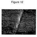
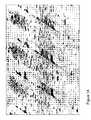
- FIGS. 12 and 13are micrographs of a nanofabric that conforms to non-planar surfaces.
- FIG. 14is an image of an exemplary nanofabric shown in perspective.
- Preferred embodiments of the inventionprovide new articles having non-horizontally-disposed nanotube articles and provide methods of making same. Some embodiments provide improved ways of clamping or pinching suspended nanotube articles to improve their performance and manufacturability. Other embodiments provide electromechanical memory cells, which may be discrete or embedded. Under some embodiments, the discrete memory cells use new approaches to connect to other circuitry or cells, which lowers the resistivity of traces to the memory cells. Still other embodiments provide memory cells that have volatile information state (i.e., the information state is lost when power is interrupted). Some other embodiments use three-trace architectures analogous to those of U.S. Patent Application Publication No.
- a nanofabric articlemay be disposed between the electrodes to cause the article to deflect toward or away from one electrode or the other.
- These embodimentsmay utilize a combination of volatile and non-volatile characteristics; for example, information state may be non-volatile, but the device may use a three-trace architecture in which the deflection of the nanotube article may be caused by a trace having volatile state characteristics.
- Nanofabrics or ribbons, created by growth or application of individual tubeshave been shown to substantially conform to substrate surfaces, such as a surface of a semiconductor substrate.
- Preferred embodiments of the presentmake devices such as electro-mechanical switches and memory cells using nanofabrics that conform to a surface which is substantially perpendicular to a semiconductor substrate (i.e. the nanofabrics are vertically-oriented, relative to a horizontal substrate).
- Devices and fabrication techniques to develop such vertically-disposed devicesare described below, and include the ability to form switches and memory cells having relatively short spans of vertically suspended nanofabric articles with corresponding reductions in gap heights.
- the articlesare substantially a monolayer of carbon nanotubes.
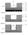
- FIGS. 1A-Bare perspective and cross-sectional views of an exemplary electromechanical switch.
- Structure 100depicts an “off” state and structure 110 (FIG. 1 (B)) depicts an “on” state.
- the designations “on” and “off”are in some sense arbitrary, and this notation may be reversed with no loss of generality.
- the structurecontains nanofabric article 102 spanning between an upper insulating support structure 104 and a lower insulating support structure 106 . Disposed between upper and lower insulating support structures 104 and 106 is an electrode 108 .
- nanofabricsuch as nanofabric article 102
- nanofabric article 102is generally meant to include any suitable structure or article comprising nanotubes, and specifically includes ribbons and nanofabric electrodes containing nanotubes.
- a nanofabric article 102has a span T of less than about 180 nm or smaller and is pinned to insulating support structures 104 and 106 (seen more clearly in FIG. 5 L).
- the span of nanofabricwill depend on deposition technique used, and under certain embodiments suspended spans can be shorter than lithographically-produced spans. The inventors envision vertical spans as small or smaller than 30 nm. Pinning of nanofabric articles is described here and elsewhere in the incorporated references in more detail.
- the electrode 108may be made of any suitable electrically conductive material and may be arranged in any of a variety of suitable geometries.
- Certain preferred embodimentsutilize n-doped silicon to form such a conductive element which can be, preferably no wider than the nanofabric article 102 , e.g., about 180 nm or below.
- Other embodimentsutilize metal as conductor.
- the electrode 108can be constructed from a nanofabric as well.
- the material of the insulating support structures 104 and 106may be made of a variety of materials and into various geometries, but certain preferred embodiments utilize insulating material, such as spin-on-glass (SOG) or silicon nitride or silicon oxide.
- SOGspin-on-glass
- silicon nitridesilicon oxide
- the nanofabric article 102is held to the insulating support structures by friction.
- the nanofabric article 102may be held by other means, such as by anchoring, stitching or pinning the nanofabric to the insulating support structures using any of a variety of techniques.
- the nanofabric article 102may be coupled to another material by introducing a matrix material into the spaces between nanotubes in a porous nanofabric to form a conducting composite junction, as described in the references incorporated above. Electrical and mechanical advantages may be obtained by using such composite junctions and connections.
- a conducting materialis deposited onto the nanofabric and is allowed to penetrate into the spaces within the porous nanofabric, thus forming an improved electrical connection to the nanofabric and reduces contact resistance in the article.
- an insulating materialis deposited onto the nanofabric and is allowed to penetrate into the spaces within the porous nanofabric, thus forming an improved mechanical pinning contact that increases reliability and manufacturability.
- Evaporated or spin-coated materialsuch as metals, semiconductors or insulators especially—silicon, titanium, silicon oxide or polyamide—may be used to increase the pinning strength.
- the friction interactioncan be increased through the use of chemical interactions, including covalent bonding through the use of carbon compounds such as pyrenes or other chemically reactive species.
- carbon compoundssuch as pyrenes or other chemically reactive species.
- a memory or logic cell, switch or relayIn some embodiments in which a nanofabric article 102 is spaced apart from and crosses a corresponding, oppositely-disposed electrode, the intersection defines a memory or logic cell, switch or relay. More than one memory cell can be used in arrays or as individual or small groups of interconnected switches depending upon the application such as embedded memory, a two-chip memory device, relays or actuators. The actual number of such cells is immaterial to understanding the invention, but the technology may support devices having information storage capacities at least on the order of modern nonvolatile circuit devices.
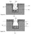
- FIGS. 2A-4Care cross-sectional diagrams of individual nanoswitches illustrating various states of the device.
- FIGS. 2A-Billustrate nanoswitches with different gap distances 202 and 208 between nanofabric article 102 and electrodes 204 and 210 , respectively.
- the vertical spacing between the insulating support structures 104 and 106is less than 180 nm; this height is dependent upon the deposition technique used.
- the relative separation, i.e. gap distance 202from the top of insulating support structure 104 to the deflected position where the nanofabric article 102 attaches to electrode 204 should be approximately 5-50 nm. In switches with smaller spans, the gap would likely also be smaller.
- the magnitude of the gap distance 202is designed to be compatible with electromechanical switching capabilities of the memory device or other electronic application.
- the 5-50 nm gap distanceis preferred for certain embodiments utilizing nanofabrics 102 made from carbon nanotubes, and reflects the specific interplay between strain energy and adhesion energy for the deflected nanotubes. Other gap distances may be preferable for other materials. Switching between these states is accomplished by the application of specific voltages across the nanofabric article 102 and one or more of its associated electrodes, e.g. 204 , 210 . Switching forces are based on the interplay of electrostatic attraction and repulsion between the nanofabric article 102 and the electrodes, e.g. 204 , 210 .
- the nanofabric article 102can remain in permanent “non-volatile” contact with the electrode 204 . If a larger gap distance 208 were selected, the strain energy increases to such an extent as to allow the nanofabric article 102 to contact the electrode 210 but not to remain in such contact without additional power input, defining a “volatile” condition. In some embodiments, such a volatile switch is preferred and can be combined with non-volatile switches as is necessary to generate particular electronic devices.
- the dimensions given aboveare exemplary and non-limiting, and can be greater or smaller in some embodiments, depending on the application and materials and techniques used.
- the length of the nanofabric article 102 in these and other vertically-disposed articlescan be quite short in comparison to other types of nanofabric articles.
- thin film techniquessuch as thin film deposition or etching can be used rather than using lithographic techniques to form the electrodes and gaps spanned by the suspended nanofabric ribbons.
- the suspended lengthcan be shorter than the length of the nanofabrics used in horizontally disposed devices, such as those in the incorporated reference entitled “Electro-Mechanical Switches and Memory Cells Using Horizontally-Disposed Nanofabric Articles and Methods of Making the Same” (U.S. Provisional Pat. Apl. Ser. No. 60/446783), filed on Feb. 12, 2003; filed on even date herewith U.S. Apl. Ser. No. yet to be assigned).
- the dependence on thin film deposition rather than lithographic patterning of the devicesmakes for more facile manufacturing.
- a short span of nanofabriccan lead to enhanced reliability and vastly increased switching speeds up to 200 GHz for concomitantly lowered gap heights. Also, shorter spans of nanofabric result in reduced electrical resistance to current flowing through the nanofabric. Further embodiments, below, illustrate other types of vertically-disposed articles, and methods of manufacturing the same.
- FIGS. 3A-Cillustrate two possible “on” states of certain embodiments of the invention.
- the nanofabric article 102is separated from both electrodes 304 and 306 by a distance 202 .
- This statemay be electrically detected in any of a variety of ways described in the foregoing references incorporated by reference.
- an “off” statecorresponds to nanofabric-electrode junction being an open circuit, which may be sensed as such on either the nanofabric article 102 or electrode 304 when addressed.
- the cellis as shown by 308 ( FIG. 3B , structure 310 )
- the nanofabric article 102is deflected toward electrode 304 .
- the “on” states corresponding to the nanofabric-electrode junctionis an electrically conducting, rectifying junction (e.g., Schottky or PN), which may be sensed as such on either the nanofabric article 102 or electrode 306 when addressed.
- PNelectrically conducting, rectifying junction
- the nanofabric article 102is deflected toward electrode 306 generating an “on” state.
- the figuresare not drawn to scale, and the distances 202 , for example, need not be equal.
- one or the other of the electrodesmay act as “set” electrode used alone or in combination with the other electrode to cause the nanotube article to deflect into contact with an electrode, and the other of the electrodes may act as a “release” electrode used alone or in combination with the other electrode to cause the nanotube article to release from contact with the electrode.
- FIGS. 4A-Cillustrate some other possible tristate or tri-trace device configurations.
- a first tri-trace device 400( FIG. 4A ) has two non-volatile “on” states.
- the distance 202 between the non-deflected nanofabric article 102 and either electrode 402 or 404is small enough that upon deflection the nanofabric contacts either electrode 402 or 404 .
- a stable van der Waals interactionis formed yielding a non-volatile condition in which the deflected nanofabric article 102 contacts either electrode, closing a circuit and remaining in contact with the electrode indefinitely without the need for additional power.
- a second tri-trace device 406( FIG. 4B ) allows for nanofabric deflection to be either non-volatile or volatile. If the nanofabric article 102 deflects toward electrode 410 , then the distance 202 is small enough to allow for a nonvolatile state as above.
- the gap distance 208between the nanofabric article 102 and the contacted electrode 408 has been increased such that the strain energy of the stretched nanofabric article 102 overcomes the van der Waals attraction between the nanofabric article 102 and the electrode 408 ; the nanofabric article 102 briefly forms part of a closed circuit generating a transient “on” state and returns to its non-deflected, open circuit state generating an “off” state.
- compare structure 400which may be used as non-volatile switch, to structure 406 , which includes a volatile switch with gap 208 .
- structure 406the gap height 208 between the nanofabric and the electrode 408 has been increased such that the strain energy of the stretched nanofabric overcomes the van der Waals attraction between the fabric and the electrode.
- the nanofabricforms part of a closed circuit and returns to its non-deflected, open circuit state.
- the effect of the van der Waals interaction between nanofabrics and other elementscan be affected at their interface(s).
- the effectmay be enhanced or diminished; e.g., the attractive force can be diminished by coating the surface of the electrode with a thin layer of oxide or other suitable materials.
- a purpose of this diminishing of attractive forcesmay be to create volatile nanoswitches; such volatile switches may be especially useful in applications such as relays, sensors, transistors, etc.
- Structure 412( FIG. 4C ) illustrates yet a third tri-trace device where the gap distances 208 between the nanofabric article 102 and the electrodes 414 and 416 are large enough to form volatile nanoswitches as described above.
- the differences between resistances in the “off” and “on” statesprovides a means to read which state a junction is in.
- a “readout” currentis applied to the nanofabric or electrode and the voltage across the junction is determined with a “sense amplifier” on the electrodes. Reads are non-destructive, meaning that the cell retains its state, and no write-back operations are needed as is required with semiconductor DRAMs.
- the three-trace junctions of preferred embodimentsbring their own advantages. By allowing for use of tristate memory cells, more information may be stored or represented by a given cell. Moreover, even if only one of the “on” states were used, three-trace junctions may increase switching speeds from the ability to use both conductive traces in concert to apply forces to move an electromechanically responsive nanofabric 102 .
- the structures as shown in FIGS. 3 and 4(generally) facilitate packaging and distribution, and allow the nanotube-technology cells to be more easily incorporated into other circuits and systems such as hybrid circuits.
- the vertical nature of the electrical architecturecan also facilitate the production of stackable memory layers and the simplification of various interconnects.
- the nanotube patch or segmentis clamped (above and below) up to the portion of the nanofabric article that is so suspended.
- the nanofabric articleis connected or joined to high conductivity signal paths.
- One aspect of the present inventionis directed to formation of conductive composite junctions whereby a suitable matrix material is disposed within and around the nanotubes or fibers of a nanofabric or other porous nano material.
- Such junctionscan provide desirable mechanical and/or electrical properties. For example, electrical contact between a nanofabric and a metal connection or activation point may be enhanced, or the contact resistance may be decreased by applying the metal contact as a matrix material impregnating the nanofabric tubes. Also, mechanical contact and strain may be increased as a result of the increased contact between the nanotubes and the matrix material.
- FIGS. 5A-Lcollectively, illustrate an exemplary method of fabricating a substantially vertical nano-electromechanical switch.
- verticalit is meant that the switching element is substantially perpendicular to the major surface of the substrate.
- This aspectwill be illustrated and described in detail below. Certain advantages can be realized in manufacturing such device using conformal nanotube and/or nanofabric materials. As a result, the length of the nanofabric article can be reduced in some embodiments by about two orders of magnitude. Additionally, the electrical resistance of a current-carrying nanofabric article is substantially reduced when the length of the article is reduced, as described herein.
- a semiconductor substrate 501 coated with an insulating layer 502 such as silicon dioxide or silicon nitrideis provided.
- the insulating layer 502is preferably a few nanometers in thickness but could be as much 1 ⁇ m thick depending upon the electrical characteristics desired for different applications.
- a second layer 504is deposited on insulating layer 502 .
- Two non-exclusive examples of the material the second layer 504 can be made fromare metals and semiconductors; the second layer having a top surface 506 .
- a cavity 507is defined in the second layer 504 .
- the cavity 507can be created by reactive ion etching into the second layer 504 ; the cavity 507 is defined by inner walls 508 and an exposed top surface 510 of insulating layer 502 .
- a portion of second layer 504remains such that the bottom of the cavity 507 is conductive.
- an insulating layer 502could be provided to top surface 506 which could be etched to generate a cavity.
- the cavity 507can be prefabricated as part of a trench or a via provided as part of preprocessing steps, e.g., as part of an overall integration scheme in generation of an electronic device.
- FIG. 5Billustrates a first insulating layer 512 made of silicon nitride or other material deposited on top of the exposed top surface 510 and top surface 506 to generate top layer 514 of intermediate structure 516 .
- the first insulating layer 512is selectively etchable over polysilicon, nanotubes and silicon oxide or other selected insulator.
- a first insulating layer 512 which will act as a sacrificial layer to create a gap between subsequent layerscan be in a range of thicknesses described below as shown in intermediate structure 516 .
- FIG. 5Cillustrates a monolayer of nanofabric 518 applied to intermediate structure 516 , forming intermediate structure 520 .
- the nanofabric 518may be applied by chemical vapor deposition, spin coating of suspensions of nanotubes, aerosolized nanotube suspensions or dipping into a solution of suspended nanotubes.
- Nanofabric layer 518conforms to the underlying insulating layer 512 and substantially follows the geometry of cavity 507 . Examples of nanofabric articles and methods of manufacturing and using the same can be found in the previously-mentioned and incorporated references.
- the resulting structure 520thus includes two vertical portions 518 A of the nanofabric 518 which is perpendicular to the major surface of the substrate 501 . Devices created using these vertical portions substantially parallel to channel 507 side walls 508 , e.g. nano-switches, are termed “vertical” devices or switches.
- FIG. 5Dillustrates a second insulating layer 522 applied over nanofabric 518 .
- Protective insulating layer 524is deposited on top of second insulating layer 522 having top surface 526 , forming intermediate structure 528 .
- the protective insulating layer 524is not deposited on the side walls of the channel.
- the thickness of protective insulating layer 524can be, for example, on the order of 100 nm, and a non-exclusive example of the method of application of protective insulating layer 524 , which may be an oxide layer, is by sputtering or high density plasma deposition of silicon dioxide. The optimal thickness is determined by the particular application to protect the layers below the insulating layer 524 from additional etching or deposition steps.
- FIG. 5Eillustrates a polysilicon layer 530 deposited on top surface 526 of intermediate structure 528 , filling the space between walls 508 in cavity 507 .
- Polysilicon layer 530can be deposited to a height greater than that of top surface 526 in order to get the proper amount of polysilicon layer into cavity 507 , creating an overfilling condition as in intermediate structure 532 .
- Polysilicon layer 530is subsequently planarized to etched polysilicon 534 with top surface 526 of oxide layer 524 as is illustrated by intermediate structure 536 (FIG. 5 F).
- FIG. 5Gillustrates polysilicon layer 534 etched to a first depth 538 , by any appropriate method.
- An exemplary method of creating such a depthis by reactive ion etch (RIE) as shown in intermediate structure 540 ; first depth 538 later helps define one edge of a suspended nanofabric segment.
- RIEreactive ion etch
- the thickness 541 of etched polysilicon layer 534is dependent on original trench depth 509 ; for example the depth may be in a range from 200 nm to 1 micron and for applications requiring ultrahigh speed electromechanical switches, the depth would preferably be below 200 nm. This depth can be reduced using thin film manufacturing techniques, as mentioned elsewhere in this document and in the documents incorporated by reference.
- FIG. 5Hillustrates a layer of oxide 542 deposited on exposed surfaces of intermediate structure 540 .
- Horizontal portions 544 of oxide layercover trench walls and vertical oxide layers 546 cover exposed, top surfaces of polysilicon layer 534 .
- Horizontal oxide layers 544are removed, e.g., by oxide spacer etching, leaving intermediate structure 550 (FIG. 5 I).
- FIG. 5Jillustrates polysilicon layer 534 etched to a second depth 552 .
- Second depth 552may be approximately 50 nm deeper than first depth 538 .
- the defined gap 554allows exposure of regions of second insulating layer 522 as is shown in intermediate structure 556 .
- first insulating layer 512is removable, e.g. by wet etching. Removal of materials from beneath a porous nanofabric has been described by the present applicants in the patent references incorporated above. Suitable wet etching conditions to remove the layers of first insulating layer 512 and second insulating layer 522 leave a suspended nanofabric 558 having vertical height 560 as observed in intermediate structure 562 (FIG. 5 K). The wet etching may leave an overhang owing to the nature of isotropic wet etching conditions. Other techniques such as dry etching may be utilized to provide an anisotropic etching step.
- the vertical height 560is defined by the etching procedure. For a vertical height 560 of 200 nm the thicknesses of first insulating layer 512 and second insulating layer 522 would be approximately 20 nm in order to provide gap distances to create two non-volatile states. Smaller vertical gaps may be preferred in certain embodiments of the invention, e.g. 30 nm gap heights.
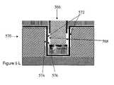
- Electrode material 566is deposited into trench 507 , leaving gaps 568 between electrode material 566 and suspended nanotube fabric 558 as shown in intermediate structure 570 (FIG. 5 L).
- the structure 570illustrates a pair of vertically-suspended nanofabric portions 572 surrounded by vertical gaps 574 , 576 on either side of each portion.
- the structuremay serve as a basis for a pair of bi- or tri-state switching devices as is explained below.
- the behavior of the switching devicesis influenced by the strain in the suspended nanofabric portions and the surrounding gap distances, as discussed herein.
- many configurations, including common electrode (e.g. 566 ) configurationsmay be obtained using the structure 570 . It is possible to split structure 570 into two discrete sections (left, right) by a vertical divide running vertically through electrode 566 for example, leaving two bi- or tri-state switches that can be independently operated.
- the nature of the resulting devices and switchesdepends on the construction and arrangement of the electrodes and connections, among other factors. Attention is called to the construction of various types of electrodes in the following embodiments, as an indication of the flexibility of the design and concepts underlying these devices and the variety of their potential uses. For example, some devices share common electrodes between more than one nanofabric article (e.g. two nanofabric switch elements being influenced by a same shared electrode). Other devices have separate electrodes that control the behavior of the nanofabric. One or more electrodes can be used with each nanofabric article to control the article, as mentioned in the incorporated reference entitled “Electromechanical Three-Trace Junction Devices” (U.S. Pat. Apl. Ser. No. 10/033,323), filed on Dec. 28, 2001.
- first insulating layer 512 and second insulating layer 522are increased to a thickness of about 50 nm the nanotube switch of certain device types would become volatile at the necessary bias voltages because the deflected nanofabric has a strain energy higher than that of the van der Waals force keeping the fabric in contact with metallic region 504 or electrode 566 .
- the thicknesses of first insulating layer 512 and second insulating layer 522can be adjusted to generate either a non-volatile or volatile condition for a given vertical gap 560 as called for by particular applications with desired electrical characteristics.
- FIG. 6illustrates an exemplary structure with subsequent layers of metallization.
- This structureincludes electrode interconnect 602 and via 604 in contact with nanofabric 518 , and a contiguous metallic layer 504 surrounding the electromechanical switch both laterally and subjacently, as shown in intermediate structure 600 .
- FIG. 7illustrates an exemplary structure with subsequent layers of metallization. This structure is similar to intermediate structure 600 in several respects. However, an insulating layer 702 separates the portions of metallic layers 504 , and therefore metallic layer 504 does not surround the electromechanical switch elements, preventing crosstalk as shown in intermediate structure 600
- FIG. 8illustrates an exemplary structure with subsequent layers of metallization. This structure is similar to intermediate structure 700 . However, the nanofabric layer 518 is not continuous, being split at the bottom and therefore there are two independent switches 802 , 804 , which have no crosstalk, as shown in intermediate structure 800 .
- FIG. 9is an exemplary structure with subsequent layers of metallization. This structure is similar to intermediate structure 800 ; however, instead of a single central electrode, there are two central electrodes, 902 , 904 separated by insulating layer 906 . Thus, intermediate structure 900 has two nano-electromechanical switches, which can be operated independently.
- Cross-sectional FIG. 10is an exemplary structure with subsequent layers of metallization. This structure is similar to intermediate structures 800 and 900 , except there is no central electrode, at all. In this embodiment, it is possible for the nanofabric switches to contact metal layers 504 to make a volatile or non-volatile switch, and it is possible for the switches to contact one another so as to be volatile or non-volatile.
- the devices and articles shown in the preceding embodimentsare given for illustrative purposes only, and other techniques may be used to produce the same or equivalents thereof.
- the articles shownmay be substituted with other types of materials and geometries in yet other embodiments.
- some embodiments of the present inventionmay employ nanotubes.
- devices comprising nanotube and nanofabric articles in place of the electrodes shown abovecan be constructed as well.
- nanofabric electrodesas contacts to portions of a transistor or as part of a transistor or to contact or become part of an interconnect for subsequent sense amplifier or addressing logic circuitry, see e.g. U.S. Pat. Apl. No. 10/379973 entitled, Hybrid Circuit Having Nanotube Electromechanical Memory.
- FIG. 6includes two distinct electrodes that will push and/or pull the vertical nanofabric sections in unison. The gap distances will determine whether the devices are volatile or nonvolatile for a given set of parameters.
- FIG. 7includes 3 distinct electrodes and gives extra degrees of freedom (extra redundancy, extra information storage capability, etc.) to the devices.
- FIG. 8also includes 3 electrodes.
- FIG. 9includes 4 distinct electrodes, since the center electrode is divided into two electrodes ( 902 , 904 ) by application of divider 906 .
- FIG. 10includes two electrodes on the sides of the channel, and uses a nanofabric section coupled to top electrode 602 as a third electrode in structure 1000 .
- the dimension T, or thickness of the electrode 108 , across which the nanofabric is suspendedis as little as a few nm thick (e.g. 10-100 nm), and is formed using thin film techniques.
- the thickness Tcan be less than 10 nm thick. Therefore, the scaling of the dimensions tracks with thin film technology rather than scaling with lithographic technology. It should be noted that the gap distances used with reduced length nanofabric articles may also be decreased accordingly.
- FIGS. 11A-Billustrate an embodiment of the present invention having an oxidized electrode.
- Structure 1110illustrates a nanofabric based switch having an insulation layer 1112 over the exposed surface of one electrode 108 .
- the insulation layer 1112may be used to change the characteristics of the switch to be volatile or to provide further assurance of desired behavior.
- FIG. 11Billustrates a structure having opposing electrodes with a nanofabric switch disposed between them.
- the insulating layer, placed on the facing surface of an opposing electrodemay be used to prevent different fibers from the nanofabric element from simultaneously electrically contacting both electrodes ( 304 , 306 ) during a state transition. Such contact may prevent or hinder switching of the fabric between states.
- FIGS. 12 and 13are micrographs of exemplary conformal nanofabrics. These figures illustrate how a fabric looks when formed and made to conform over vertical and horizontal surfaces.
- the preferred embodimentsare made using nanotube films, layers, or non-woven fabrics so that they form, or may be made to form, various useful patterned components, elements or articles.
- films,” “layers,” or “non-woven fabrics”are referred to as “fabrics” or “nanofabrics”.
- the components created from the nanofabricsretain desirable physical properties of the nanotubes and/or the nanofabrics from which they are formed.
- preferred embodimentsallow modern manufacturing techniques (e.g., those used in semiconductor manufacture) to be employed to utilize the nanofabric articles and devices.
- Preferred embodiments of the present inventioninclude articles and methods that increase a strain in the nanofabrics, allowing selectable construction of volatile and non-volatile electromechanical switches, including tri-state or tri-trace switches having both volatile and non-volatile states.
- the nanofabricsin some embodiments also provide for discrete cellular articles, such as memory cells, to be manufactured.
- FIG. 14is an image of an exemplary fabric of nanotubes shown in perspective. As can be seen, the fabric may be highly porous and appear as several threads with gaps in between. In this figure there are actually several ribbons of nanofabric extending from left to right separated from one another by areas with no nanotubes. One may notice that the fabric of FIG. 13 is likewise very porous with a few nanotubes spanning the channel and contacting electrodes. In both figures, the resolution of the figure is affected by the imaging technology so some nanotubes may not appear in focus or be noticeable.
Landscapes
- Engineering & Computer Science (AREA)
- Chemical & Material Sciences (AREA)
- Nanotechnology (AREA)
- Materials Engineering (AREA)
- Manufacturing & Machinery (AREA)
- Physics & Mathematics (AREA)
- Crystallography & Structural Chemistry (AREA)
- Condensed Matter Physics & Semiconductors (AREA)
- General Physics & Mathematics (AREA)
- Computer Hardware Design (AREA)
- Microelectronics & Electronic Packaging (AREA)
- Organic Chemistry (AREA)
- Inorganic Chemistry (AREA)
- Mathematical Physics (AREA)
- Chemical Kinetics & Catalysis (AREA)
- Theoretical Computer Science (AREA)
- Power Engineering (AREA)
- Composite Materials (AREA)
- Semiconductor Memories (AREA)
- Carbon And Carbon Compounds (AREA)
Abstract
Description
Claims (16)
Priority Applications (4)
| Application Number | Priority Date | Filing Date | Title |
|---|---|---|---|
| US10/776,572US6924538B2 (en) | 2001-07-25 | 2004-02-11 | Devices having vertically-disposed nanofabric articles and methods of making the same |
| US11/158,217US7112464B2 (en) | 2001-07-25 | 2005-06-21 | Devices having vertically-disposed nanofabric articles and methods of making the same |
| US11/158,544US7274078B2 (en) | 2001-07-25 | 2005-06-22 | Devices having vertically-disposed nanofabric articles and methods of making the same |
| US11/526,364US7719067B2 (en) | 2001-07-25 | 2006-09-25 | Devices having vertically-disposed nanofabric articles and methods of making the same |
Applications Claiming Priority (7)
| Application Number | Priority Date | Filing Date | Title |
|---|---|---|---|
| US09/915,093US6919592B2 (en) | 2001-07-25 | 2001-07-25 | Electromechanical memory array using nanotube ribbons and method for making same |
| US10/033,323US6911682B2 (en) | 2001-12-28 | 2001-12-28 | Electromechanical three-trace junction devices |
| US10/128,118US6706402B2 (en) | 2001-07-25 | 2002-04-23 | Nanotube films and articles |
| US10/341,005US7566478B2 (en) | 2001-07-25 | 2003-01-13 | Methods of making carbon nanotube films, layers, fabrics, ribbons, elements and articles |
| US44678603P | 2003-02-12 | 2003-02-12 | |
| US44678303P | 2003-02-12 | 2003-02-12 | |
| US10/776,572US6924538B2 (en) | 2001-07-25 | 2004-02-11 | Devices having vertically-disposed nanofabric articles and methods of making the same |
Related Parent Applications (4)
| Application Number | Title | Priority Date | Filing Date |
|---|---|---|---|
| US09/915,093Continuation-In-PartUS6919592B2 (en) | 2001-07-25 | 2001-07-25 | Electromechanical memory array using nanotube ribbons and method for making same |
| US10/033,323Continuation-In-PartUS6911682B2 (en) | 2001-07-25 | 2001-12-28 | Electromechanical three-trace junction devices |
| US10/128,118Continuation-In-PartUS6706402B2 (en) | 2001-07-25 | 2002-04-23 | Nanotube films and articles |
| US10/341,005Continuation-In-PartUS7566478B2 (en) | 2001-07-25 | 2003-01-13 | Methods of making carbon nanotube films, layers, fabrics, ribbons, elements and articles |
Related Child Applications (2)
| Application Number | Title | Priority Date | Filing Date |
|---|---|---|---|
| US11/158,217DivisionUS7112464B2 (en) | 2001-07-25 | 2005-06-21 | Devices having vertically-disposed nanofabric articles and methods of making the same |
| US11/158,544ContinuationUS7274078B2 (en) | 2001-07-25 | 2005-06-22 | Devices having vertically-disposed nanofabric articles and methods of making the same |
Publications (2)
| Publication Number | Publication Date |
|---|---|
| US20040175856A1 US20040175856A1 (en) | 2004-09-09 |
| US6924538B2true US6924538B2 (en) | 2005-08-02 |
Family
ID=36584495
Family Applications (3)
| Application Number | Title | Priority Date | Filing Date |
|---|---|---|---|
| US10/776,572Expired - Fee RelatedUS6924538B2 (en) | 2001-07-25 | 2004-02-11 | Devices having vertically-disposed nanofabric articles and methods of making the same |
| US11/158,217Expired - LifetimeUS7112464B2 (en) | 2001-07-25 | 2005-06-21 | Devices having vertically-disposed nanofabric articles and methods of making the same |
| US11/158,544Expired - LifetimeUS7274078B2 (en) | 2001-07-25 | 2005-06-22 | Devices having vertically-disposed nanofabric articles and methods of making the same |
Family Applications After (2)
| Application Number | Title | Priority Date | Filing Date |
|---|---|---|---|
| US11/158,217Expired - LifetimeUS7112464B2 (en) | 2001-07-25 | 2005-06-21 | Devices having vertically-disposed nanofabric articles and methods of making the same |
| US11/158,544Expired - LifetimeUS7274078B2 (en) | 2001-07-25 | 2005-06-22 | Devices having vertically-disposed nanofabric articles and methods of making the same |
Country Status (1)
| Country | Link |
|---|---|
| US (3) | US6924538B2 (en) |
Cited By (116)
| Publication number | Priority date | Publication date | Assignee | Title |
|---|---|---|---|---|
| US20050065741A1 (en)* | 2003-05-14 | 2005-03-24 | Nantero, Inc. | Sensor platform using a non-horizontally oriented nanotube element |
| US20050101112A1 (en)* | 2001-07-25 | 2005-05-12 | Nantero, Inc. | Methods of nanotubes films and articles |
| US20050281084A1 (en)* | 2001-12-28 | 2005-12-22 | Nantero, Inc. | Methods of making electromechanical three-trace junction devices |
| US20060183278A1 (en)* | 2005-01-14 | 2006-08-17 | Nantero, Inc. | Field effect device having a channel of nanofabric and methods of making same |
| US20060193093A1 (en)* | 2004-11-02 | 2006-08-31 | Nantero, Inc. | Nanotube ESD protective devices and corresponding nonvolatile and volatile nanotube switches |
| US20060204427A1 (en)* | 2004-12-16 | 2006-09-14 | Nantero, Inc. | Aqueous carbon nanotube applicator liquids and methods for producing applicator liquids thereof |
| US7112464B2 (en) | 2001-07-25 | 2006-09-26 | Nantero, Inc. | Devices having vertically-disposed nanofabric articles and methods of making the same |
| US20060231865A1 (en)* | 2001-12-28 | 2006-10-19 | Nantero, Inc. | Electromechanical three-trace junction devices |
| US20060237857A1 (en)* | 2005-01-14 | 2006-10-26 | Nantero, Inc. | Hybrid carbon nanotube FET(CNFET)-FET static RAM (SRAM) and method of making same |
| US20060250856A1 (en)* | 2005-05-09 | 2006-11-09 | Nantero, Inc. | Memory arrays using nanotube articles with reprogrammable resistance |
| US20060260785A1 (en)* | 2005-05-13 | 2006-11-23 | Delta Electronics, Inc. | Heat sink |
| US20060281256A1 (en)* | 2005-06-08 | 2006-12-14 | Carter Richard J | Self-aligned cell integration scheme |
| WO2006137876A2 (en) | 2004-09-22 | 2006-12-28 | Nantero, Inc. | Random access memory including nanotube switching elements |
| US20070004191A1 (en)* | 2005-06-30 | 2007-01-04 | Lsi Logic Corporation | Novel techniques for precision pattern transfer of carbon nanotubes from photo mask to wafers |
| US20070040491A1 (en)* | 2005-06-02 | 2007-02-22 | Ping Mei | Thin film devices and methods for forming the same |
| WO2007053180A1 (en) | 2005-05-09 | 2007-05-10 | Nantero, Inc. | Two-terminal nanotube devices and systems and methods of making same |
| US20070132046A1 (en)* | 2005-11-10 | 2007-06-14 | Samsung Electronics Co. Ltd. | Nanotube based nonvolatile memory device and a method of fabricating and operating the same |
| US20070237959A1 (en)* | 2005-09-06 | 2007-10-11 | Lemaire Charles A | Apparatus and method for growing fullerene nanotube forests, and forming nanotube films, threads and composite structures therefrom |
| US20070236325A1 (en)* | 2004-09-21 | 2007-10-11 | Nantero, Inc. | Resistive elements using carbon nanotubes |
| US7304357B2 (en) | 2001-07-25 | 2007-12-04 | Nantero, Inc. | Devices having horizontally-disposed nanofabric articles and methods of making the same |
| US20080035928A1 (en)* | 2006-08-10 | 2008-02-14 | Samsung Electronics Co., Ltd. | Vertical electromechanical memory devices and methods of manufacturing the same |
| US7335395B2 (en) | 2002-04-23 | 2008-02-26 | Nantero, Inc. | Methods of using pre-formed nanotubes to make carbon nanotube films, layers, fabrics, ribbons, elements and articles |
| US7342818B2 (en) | 2001-07-25 | 2008-03-11 | Nantero, Inc. | Hybrid circuit having nanotube electromechanical memory |
| US20080067681A1 (en)* | 2006-09-19 | 2008-03-20 | National Tsing Hua University | Interconnection structure and manufacturing method thereof |
| US20080070401A1 (en)* | 2006-09-18 | 2008-03-20 | Samsung Electronics Co., Ltd. | Memory device and method for manufacturing the same |
| US20080079027A1 (en)* | 2004-06-09 | 2008-04-03 | Nantero, Inc. | Field effect devices having a gate controlled via a nanotube switching element |
| US20080093686A1 (en)* | 2006-10-23 | 2008-04-24 | Samsung Electronics Co., Ltd. | Electromechanical non-volatile memory devices |
| US20080094895A1 (en)* | 2006-10-23 | 2008-04-24 | Samsung Electronics Co., Ltd. | Non-volatile memory device and method of fabricating the same |
| US7394687B2 (en)* | 2005-05-09 | 2008-07-01 | Nantero, Inc. | Non-volatile-shadow latch using a nanotube switch |
| US20080157257A1 (en)* | 2005-05-09 | 2008-07-03 | Nantero, Inc. | Nonvolatile nanotube diodes and nonvolatile nanotube blocks and systems using same and methods of making same |
| US20080157126A1 (en)* | 2005-05-09 | 2008-07-03 | Nantero, Inc. | Nonvolatile nanotube diodes and nonvolatile nanotube blocks and systems using same and methods of making same |
| US20080157127A1 (en)* | 2005-05-09 | 2008-07-03 | Nantero, Inc. | Nonvolatile nanotube diodes and nonvolatile nanotube blocks and systems using same and methods of making same |
| US20080170429A1 (en)* | 2005-05-09 | 2008-07-17 | Nantero, Inc. | Nonvolatile nanotube diodes and nonvolatile nanotube blocks and systems using same and methods of making same |
| US20080212361A1 (en)* | 2005-05-09 | 2008-09-04 | Nantero, Inc. | Nonvolatile nanotube diodes and nonvolatile nanotube blocks and systems using same and methods of making same |
| US20080233744A1 (en)* | 2005-09-19 | 2008-09-25 | California Institute Of Technology | Carbon nanotube switches for memory, rf communications and sensing applications, and methods of making the same |
| US20080238882A1 (en)* | 2007-02-21 | 2008-10-02 | Ramesh Sivarajan | Symmetric touch screen system with carbon nanotube-based transparent conductive electrode pairs |
| USD578536S1 (en)* | 2007-08-27 | 2008-10-14 | Podium Photonics (Guangzhou) Ltd. | Chip |
| US20080280038A1 (en)* | 2003-01-13 | 2008-11-13 | Nantero, Inc. | Methods of using thin metal layers to make carbon nanotube films, layers, fabrics, ribbons, elements and articles |
| US20080290423A1 (en)* | 2003-08-13 | 2008-11-27 | Nantero, Inc. | Nanotube-based switching element |
| KR100878016B1 (en)* | 2007-06-27 | 2009-01-13 | 삼성전자주식회사 | Switch element and its manufacturing method |
| US20090014803A1 (en)* | 2007-07-10 | 2009-01-15 | International Business Machines Corporation | Nanoelectromechanical transistors and methods of forming same |
| US20090017572A1 (en)* | 2007-07-11 | 2009-01-15 | International Business Machines Corporation | Nanoelectromechanical transistors and methods of forming same |
| US20090051032A1 (en)* | 2003-09-08 | 2009-02-26 | Segal Brent M | Patterned nanoscopic articles and methods of making the same |
| US20090099016A1 (en)* | 2005-12-19 | 2009-04-16 | Advanced Technology Materials, Inc. | Production of carbon nanotubes |
| US20090115305A1 (en)* | 2007-05-22 | 2009-05-07 | Nantero, Inc. | Triodes using nanofabric articles and methods of making the same |
| US20090140167A1 (en)* | 2005-09-06 | 2009-06-04 | Natero, Inc. | Nanotube fabric-based sensor systems and methods of making same |
| US20090173964A1 (en)* | 2001-07-25 | 2009-07-09 | Nantero, Inc. | Method of forming a carbon nanotube-based contact to semiconductor |
| US7560136B2 (en) | 2003-01-13 | 2009-07-14 | Nantero, Inc. | Methods of using thin metal layers to make carbon nanotube films, layers, fabrics, ribbons, elements and articles |
| US20090184389A1 (en)* | 2005-05-09 | 2009-07-23 | Bertin Claude L | Nonvolatile Nanotube Diodes and Nonvolatile Nanotube Blocks and Systems Using Same and Methods of Making Same |
| US7566478B2 (en) | 2001-07-25 | 2009-07-28 | Nantero, Inc. | Methods of making carbon nanotube films, layers, fabrics, ribbons, elements and articles |
| US20090211460A1 (en)* | 2007-11-20 | 2009-08-27 | Kwok Kuen So | Bowl and basket assembly and salad spinner incorporating such an assembly |
| EP2104108A1 (en) | 2006-08-08 | 2009-09-23 | Nantero, Inc. | Nonvolatile resistive memories, latch circuits, and operation circuits having scalable two-terminal nanotube switches |
| US7598127B2 (en) | 2005-05-12 | 2009-10-06 | Nantero, Inc. | Nanotube fuse structure |
| US20090256594A1 (en)* | 2008-04-09 | 2009-10-15 | International Business Machines Corporation | Nanoelectromechanical digital inverter |
| US20090303337A1 (en)* | 2003-07-18 | 2009-12-10 | Katsumi Kaneko | Image pick-up device and synchronization-signal-generating device |
| US20100001267A1 (en)* | 2008-06-20 | 2010-01-07 | Nantero, Inc. | Nram arrays with nanotube blocks, nanotube traces, and nanotube planes and methods of making same |
| US20100012927A1 (en)* | 2001-07-25 | 2010-01-21 | Nantero, Inc. | Devices having vertically-disposed nanofabric articles and methods of making the same |
| US20100038625A1 (en)* | 2008-08-14 | 2010-02-18 | Nantero, Inc. | Nonvolatile nanotube programmable logic devices and a nonvolatile nanotube field programmable gate array using same |
| US20100061143A1 (en)* | 2006-09-22 | 2010-03-11 | Carley L Richard | Assembling and Applying Nano-Electro-Mechanical Systems |
| US20100072042A1 (en)* | 2005-05-09 | 2010-03-25 | Bertin Claude L | Memory elements and cross point switches and arrays of same using nonvolatile nanotube blocks |
| US20100072957A1 (en)* | 2004-06-18 | 2010-03-25 | Bertin Claude L | Nanotube-based logic driver circuits |
| US20100147657A1 (en)* | 2004-11-02 | 2010-06-17 | Nantero, Inc. | Nanotube esd protective devices and corresponding nonvolatile and volatile nanotube switches |
| US7744793B2 (en) | 2005-09-06 | 2010-06-29 | Lemaire Alexander B | Apparatus and method for growing fullerene nanotube forests, and forming nanotube films, threads and composite structures therefrom |
| US7745810B2 (en) | 2001-07-25 | 2010-06-29 | Nantero, Inc. | Nanotube films and articles |
| US20100165737A1 (en)* | 2006-08-07 | 2010-07-01 | Samsung Electronics Co., Ltd. | Electromechanical memory devices and methods of manufacturing the same |
| US7790494B2 (en) | 2007-01-16 | 2010-09-07 | Samsung Electronics Co., Ltd. | Method of fabricating a multi-bit electro-mechanical memory device |
| US20100267205A1 (en)* | 2005-09-06 | 2010-10-21 | Lockheed Martin Corporation | Carbon nanotubes for the selective transfer of heat from electronics |
| US20100320564A1 (en)* | 2006-03-08 | 2010-12-23 | Samsung Electronics Co., Ltd. | Nanowire memory device and method of manufacturing the same |
| US7858185B2 (en) | 2003-09-08 | 2010-12-28 | Nantero, Inc. | High purity nanotube fabrics and films |
| US20100327247A1 (en)* | 2005-09-06 | 2010-12-30 | Nantero, Inc. | Method and system of using nanotube fabrics as joule heating elements for memories and other applications |
| US20110027497A1 (en)* | 2009-07-31 | 2011-02-03 | Nantero, Inc. | Anisotropic nanotube fabric layers and films and methods of forming same |
| US20110034008A1 (en)* | 2009-08-07 | 2011-02-10 | Nantero, Inc. | Method for forming a textured surface on a semiconductor substrate using a nanofabric layer |
| US20110056812A1 (en)* | 2009-09-08 | 2011-03-10 | Kaul Anupama B | Nano-electro-mechanical switches using three-dimensional sidewall-conductive carbon nanofibers and method for making the same |
| US20110057717A1 (en)* | 2007-06-22 | 2011-03-10 | Nantero, Inc. | Two-terminal nanotube devices including a nanotube bridge and methods of making same |
| US7915637B2 (en) | 2008-11-19 | 2011-03-29 | Nantero, Inc. | Switching materials comprising mixed nanoscopic particles and carbon nanotubes and method of making and using the same |
| US7928521B1 (en) | 2005-05-31 | 2011-04-19 | Nantero, Inc. | Non-tensioned carbon nanotube switch design and process for making same |
| US20110096587A1 (en)* | 2009-10-23 | 2011-04-28 | Nantero, Inc. | Dynamic sense current supply circuit and associated method for reading and characterizing a resistive memory array |
| US7965156B2 (en) | 2005-09-06 | 2011-06-21 | Nantero, Inc. | Carbon nanotube resonators comprising a non-woven fabric of unaligned nanotubes |
| US20110156009A1 (en)* | 2009-12-31 | 2011-06-30 | Manning H Montgomery | Compact electrical switching devices with nanotube elements, and methods of making same |
| US20110163290A1 (en)* | 2009-10-23 | 2011-07-07 | Nantero, Inc. | Methods for passivating a carbonic nanolayer |
| US7986546B2 (en) | 2005-05-09 | 2011-07-26 | Nantero, Inc. | Non-volatile shadow latch using a nanotube switch |
| US20110203632A1 (en)* | 2010-02-22 | 2011-08-25 | Rahul Sen | Photovoltaic devices using semiconducting nanotube layers |
| US20110212535A1 (en)* | 2010-01-13 | 2011-09-01 | Kaul Anupama B | Applications and methods of operating a three-dimensional nano-electro-mechanical resonator and related devices |
| US8101976B2 (en) | 2001-07-25 | 2012-01-24 | Nantero Inc. | Device selection circuitry constructed with nanotube ribbon technology |
| US8110883B2 (en) | 2007-03-12 | 2012-02-07 | Nantero Inc. | Electromagnetic and thermal sensors using carbon nanotubes and methods of making same |
| US8125824B1 (en) | 2010-09-02 | 2012-02-28 | Lockheed Martin Corporation | Nanotube random access memory (NRAM) and transistor integration |
| US8147722B2 (en) | 2003-09-08 | 2012-04-03 | Nantero Inc. | Spin-coatable liquid for formation of high purity nanotube films |
| US8183665B2 (en) | 2005-11-15 | 2012-05-22 | Nantero Inc. | Nonvolatile nanotube diodes and nonvolatile nanotube blocks and systems using same and methods of making same |
| US8253171B1 (en) | 2009-08-27 | 2012-08-28 | Lockheed Martin Corporation | Two terminal nanotube switch, memory array incorporating the same and method of making |
| US8350360B1 (en) | 2009-08-28 | 2013-01-08 | Lockheed Martin Corporation | Four-terminal carbon nanotube capacitors |
| US8405189B1 (en) | 2010-02-08 | 2013-03-26 | Lockheed Martin Corporation | Carbon nanotube (CNT) capacitors and devices integrated with CNT capacitors |
| US8471238B2 (en) | 2004-09-16 | 2013-06-25 | Nantero Inc. | Light emitters using nanotubes and methods of making same |
| US8493081B2 (en) | 2009-12-08 | 2013-07-23 | Magna Closures Inc. | Wide activation angle pinch sensor section and sensor hook-on attachment principle |
| US8574673B2 (en) | 2009-07-31 | 2013-11-05 | Nantero Inc. | Anisotropic nanotube fabric layers and films and methods of forming same |
| US8791778B2 (en)* | 2009-04-20 | 2014-07-29 | International Business Machines Corporation | Vertical integrated circuit switches, design structure and methods of fabricating same |
| US8895950B2 (en) | 2009-10-23 | 2014-11-25 | Nantero Inc. | Methods for passivating a carbonic nanolayer |
| US8937575B2 (en) | 2009-07-31 | 2015-01-20 | Nantero Inc. | Microstrip antenna elements and arrays comprising a shaped nanotube fabric layer and integrated two terminal nanotube select devices |
| US8941094B2 (en) | 2010-09-02 | 2015-01-27 | Nantero Inc. | Methods for adjusting the conductivity range of a nanotube fabric layer |
| US9196766B1 (en) | 2012-04-25 | 2015-11-24 | Magnolia Optical Technologies, Inc. | Thermal detectors using graphene and oxides of graphene and methods of making the same |
| US9234979B2 (en) | 2009-12-08 | 2016-01-12 | Magna Closures Inc. | Wide activation angle pinch sensor section |
| US9299430B1 (en) | 2015-01-22 | 2016-03-29 | Nantero Inc. | Methods for reading and programming 1-R resistive change element arrays |
| US9362390B2 (en) | 2010-02-22 | 2016-06-07 | Nantero, Inc. | Logic elements comprising carbon nanotube field effect transistor (CNTFET) devices and methods of making same |
| US9390790B2 (en) | 2005-04-05 | 2016-07-12 | Nantero Inc. | Carbon based nonvolatile cross point memory incorporating carbon based diode select devices and MOSFET select devices for memory and logic applications |
| US9422651B2 (en) | 2003-01-13 | 2016-08-23 | Nantero Inc. | Methods for arranging nanoscopic elements within networks, fabrics, and films |
| US9574290B2 (en) | 2003-01-13 | 2017-02-21 | Nantero Inc. | Methods for arranging nanotube elements within nanotube fabrics and films |
| US9617151B2 (en) | 2010-02-12 | 2017-04-11 | Nantero Inc. | Methods for controlling density, porosity, and/or gap size within nanotube fabric layers and films |
| US9634251B2 (en) | 2012-02-27 | 2017-04-25 | Nantero Inc. | Nanotube solution treated with molecular additive, nanotube film having enhanced adhesion property, and methods for forming the nanotube solution and the nanotube film |
| US9650732B2 (en) | 2013-05-01 | 2017-05-16 | Nantero Inc. | Low defect nanotube application solutions and fabrics and methods for making same |
| US9666272B2 (en) | 2009-08-06 | 2017-05-30 | Nantero Inc. | Resistive change element arrays using resistive reference elements |
| US9911743B2 (en) | 2005-05-09 | 2018-03-06 | Nantero, Inc. | Nonvolatile nanotube diodes and nonvolatile nanotube blocks and systems using same and methods of making same |
| US9934848B2 (en) | 2016-06-07 | 2018-04-03 | Nantero, Inc. | Methods for determining the resistive states of resistive change elements |
| US9941001B2 (en) | 2016-06-07 | 2018-04-10 | Nantero, Inc. | Circuits for determining the resistive states of resistive change elements |
| US10069072B2 (en) | 2010-09-20 | 2018-09-04 | Nantero, Inc. | Nanotube solutions with high concentration and low contamination and methods for purifiying nanotube solutions |
| US10654718B2 (en) | 2013-09-20 | 2020-05-19 | Nantero, Inc. | Scalable nanotube fabrics and methods for making same |
| US10661304B2 (en) | 2010-03-30 | 2020-05-26 | Nantero, Inc. | Microfluidic control surfaces using ordered nanotube fabrics |
| US10920085B2 (en) | 2016-01-20 | 2021-02-16 | Honda Motor Co., Ltd. | Alteration of carbon fiber surface properties via growing of carbon nanotubes |
Families Citing this family (48)
| Publication number | Priority date | Publication date | Assignee | Title |
|---|---|---|---|---|
| US7113426B2 (en)* | 2003-03-28 | 2006-09-26 | Nantero, Inc. | Non-volatile RAM cell and array using nanotube switch position for information state |
| US6944054B2 (en)* | 2003-03-28 | 2005-09-13 | Nantero, Inc. | NRAM bit selectable two-device nanotube array |
| EP1609188A4 (en) | 2003-03-28 | 2007-11-07 | Nantero Inc | Nanotube-on-gate fet structures and applications |
| US7294877B2 (en)* | 2003-03-28 | 2007-11-13 | Nantero, Inc. | Nanotube-on-gate FET structures and applications |
| US7075141B2 (en)* | 2003-03-28 | 2006-07-11 | Nantero, Inc. | Four terminal non-volatile transistor device |
| US6995046B2 (en) | 2003-04-22 | 2006-02-07 | Nantero, Inc. | Process for making byte erasable devices having elements made with nanotubes |
| US7045421B2 (en)* | 2003-04-22 | 2006-05-16 | Nantero, Inc. | Process for making bit selectable devices having elements made with nanotubes |
| US7301802B2 (en)* | 2003-06-09 | 2007-11-27 | Nantero, Inc. | Circuit arrays having cells with combinations of transistors and nanotube switching elements |
| US7274064B2 (en)* | 2003-06-09 | 2007-09-25 | Nanatero, Inc. | Non-volatile electromechanical field effect devices and circuits using same and methods of forming same |
| EP1665278A4 (en)* | 2003-08-13 | 2007-11-07 | Nantero Inc | NANOTUBE SWITCHING ELEMENTS COMPRISING MULTIPLE CONTROLS AND CIRCUITS PRODUCED FROM THESE ELEMENTS |
| US7289357B2 (en)* | 2003-08-13 | 2007-10-30 | Nantero, Inc. | Isolation structure for deflectable nanotube elements |
| CN1868002B (en)* | 2003-08-13 | 2011-12-14 | 南泰若股份有限公司 | Nanotube-based switching element with multiple controls and circuits made therefrom |
| WO2005017967A2 (en)* | 2003-08-13 | 2005-02-24 | Nantero, Inc. | Nanotube device structure and methods of fabrication |
| US7504051B2 (en)* | 2003-09-08 | 2009-03-17 | Nantero, Inc. | Applicator liquid for use in electronic manufacturing processes |
| US7528437B2 (en)* | 2004-02-11 | 2009-05-05 | Nantero, Inc. | EEPROMS using carbon nanotubes for cell storage |
| US7658869B2 (en)* | 2004-06-03 | 2010-02-09 | Nantero, Inc. | Applicator liquid containing ethyl lactate for preparation of nanotube films |
| US7556746B2 (en)* | 2004-06-03 | 2009-07-07 | Nantero, Inc. | Method of making an applicator liquid for electronics fabrication process |
| GB0413310D0 (en)* | 2004-06-15 | 2004-07-14 | Koninkl Philips Electronics Nv | Nanowire semiconductor device |
| US7167026B2 (en)* | 2004-06-18 | 2007-01-23 | Nantero, Inc. | Tri-state circuit using nanotube switching elements |
| US7330709B2 (en)* | 2004-06-18 | 2008-02-12 | Nantero, Inc. | Receiver circuit using nanotube-based switches and logic |
| US7329931B2 (en)* | 2004-06-18 | 2008-02-12 | Nantero, Inc. | Receiver circuit using nanotube-based switches and transistors |
| US7161403B2 (en) | 2004-06-18 | 2007-01-09 | Nantero, Inc. | Storage elements using nanotube switching elements |
| US7288970B2 (en) | 2004-06-18 | 2007-10-30 | Nantero, Inc. | Integrated nanotube and field effect switching device |
| US7652342B2 (en)* | 2004-06-18 | 2010-01-26 | Nantero, Inc. | Nanotube-based transfer devices and related circuits |
| US7575693B2 (en)* | 2005-05-23 | 2009-08-18 | Nantero, Inc. | Method of aligning nanotubes and wires with an etched feature |
| US7402770B2 (en) | 2005-06-10 | 2008-07-22 | Lsi Logic Corporation | Nano structure electrode design |
| US7352607B2 (en)* | 2005-07-26 | 2008-04-01 | International Business Machines Corporation | Non-volatile switching and memory devices using vertical nanotubes |
| DE102006004218B3 (en)* | 2006-01-30 | 2007-08-16 | Infineon Technologies Ag | Electromechanical storage device and method for manufacturing an electromechanical storage device |
| US7492046B2 (en)* | 2006-04-21 | 2009-02-17 | International Business Machines Corporation | Electric fuses using CNTs (carbon nanotubes) |
| US7534648B2 (en)* | 2006-06-29 | 2009-05-19 | Intel Corporation | Aligned nanotube bearing composite material |
| US7751663B2 (en)* | 2006-09-21 | 2010-07-06 | Uni-Pixel Displays, Inc. | Backside reflection optical display |
| US7560344B2 (en)* | 2006-11-15 | 2009-07-14 | Samsung Electronics Co., Ltd. | Semiconductor device having a pair of fins and method of manufacturing the same |
| FR2910706B1 (en)* | 2006-12-21 | 2009-03-20 | Commissariat Energie Atomique | INTERCONNECTION ELEMENT BASED ON CARBON NANOTUBES |
| US7667999B2 (en) | 2007-03-27 | 2010-02-23 | Sandisk 3D Llc | Method to program a memory cell comprising a carbon nanotube fabric and a steering element |
| US7982209B2 (en) | 2007-03-27 | 2011-07-19 | Sandisk 3D Llc | Memory cell comprising a carbon nanotube fabric element and a steering element |
| JP2009135328A (en)* | 2007-11-30 | 2009-06-18 | Toshiba Corp | Nonvolatile semiconductor memory device |
| US20090166610A1 (en)* | 2007-12-31 | 2009-07-02 | April Schricker | Memory cell with planarized carbon nanotube layer and methods of forming the same |
| US9019756B2 (en)* | 2008-02-14 | 2015-04-28 | Cavendish Kinetics, Ltd | Architecture for device having cantilever electrode |
| FR2930370B1 (en)* | 2008-04-18 | 2011-08-26 | Thales Sa | MICROSYSTEM COMPONENTS COMPRISING A MEMBRANE COMPRISING NANOTUBES. |
| EP2345052A2 (en)* | 2008-10-01 | 2011-07-20 | Joseph F. Pinkerton | Nanoelectromechanical tunneling current switch |
| US8535544B2 (en) | 2010-07-26 | 2013-09-17 | International Business Machines Corporation | Structure and method to form nanopore |
| US8138068B2 (en) | 2010-08-11 | 2012-03-20 | International Business Machines Corporation | Method to form nanopore array |
| CN101912848B (en)* | 2010-08-25 | 2012-06-20 | 清华大学 | Electric-braking cleaning device |
| CN102403304B (en)* | 2011-12-06 | 2016-03-16 | 上海集成电路研发中心有限公司 | A kind of interconnection structure and preparation method thereof |
| EP2887355A1 (en)* | 2013-12-20 | 2015-06-24 | IMEC vzw | Data storage cell and memory arrangement |
| US9228994B1 (en) | 2014-08-06 | 2016-01-05 | Globalfoundries Inc. | Nanochannel electrode devices |
| FR3086386B1 (en)* | 2018-09-21 | 2020-12-04 | Commissariat Energie Atomique | MEASURING DEVICE CONTAINING A SUSPENDED SEMICONDUCTOR WIRE |
| WO2024137870A1 (en)* | 2022-12-22 | 2024-06-27 | nEYE Systems, Inc. | Dual layer optical switch |
Citations (29)
| Publication number | Priority date | Publication date | Assignee | Title |
|---|---|---|---|---|
| US6128214A (en) | 1999-03-29 | 2000-10-03 | Hewlett-Packard | Molecular wire crossbar memory |
| US6159620A (en) | 1997-03-31 | 2000-12-12 | The Regents Of The University Of California | Single-electron solid state electronic device |
| WO2001003208A1 (en) | 1999-07-02 | 2001-01-11 | President And Fellows Of Harvard College | Nanoscopic wire-based devices, arrays, and methods of their manufacture |
| US6183714B1 (en) | 1995-09-08 | 2001-02-06 | Rice University | Method of making ropes of single-wall carbon nanotubes |
| US6198655B1 (en) | 1999-12-10 | 2001-03-06 | The Regents Of The University Of California | Electrically addressable volatile non-volatile molecular-based switching devices |
| US6221330B1 (en) | 1997-08-04 | 2001-04-24 | Hyperion Catalysis International Inc. | Process for producing single wall nanotubes using unsupported metal catalysts |
| US6232706B1 (en) | 1998-11-12 | 2001-05-15 | The Board Of Trustees Of The Leland Stanford Junior University | Self-oriented bundles of carbon nanotubes and method of making same |
| WO2001044796A1 (en) | 1999-12-15 | 2001-06-21 | Board Of Trustees Of The Leland Stanford Junior University | Carbon nanotube devices |
| US6445006B1 (en) | 1995-12-20 | 2002-09-03 | Advanced Technology Materials, Inc. | Microelectronic and microelectromechanical devices comprising carbon nanotube components, and methods of making same |
| US20020130311A1 (en) | 2000-08-22 | 2002-09-19 | Lieber Charles M. | Doped elongated semiconductors, growing such semiconductors, devices including such semiconductors and fabricating such devices |
| US20020172963A1 (en) | 2001-01-10 | 2002-11-21 | Kelley Shana O. | DNA-bridged carbon nanotube arrays |
| US20020179434A1 (en) | 1998-08-14 | 2002-12-05 | The Board Of Trustees Of The Leland Stanford Junior University | Carbon nanotube devices |
| US20030021966A1 (en) | 2001-07-25 | 2003-01-30 | Segal Brent M. | Electromechanical memory array using nanotube ribbons and method for making same |
| US6518156B1 (en) | 1999-03-29 | 2003-02-11 | Hewlett-Packard Company | Configurable nanoscale crossbar electronic circuits made by electrochemical reaction |
| US6548841B2 (en)* | 2000-11-09 | 2003-04-15 | Texas Instruments Incorporated | Nanomechanical switches and circuits |
| US6559468B1 (en) | 1999-03-29 | 2003-05-06 | Hewlett-Packard Development Company Lp | Molecular wire transistor (MWT) |
| US6574130B2 (en) | 2001-07-25 | 2003-06-03 | Nantero, Inc. | Hybrid circuit having nanotube electromechanical memory |
| US20030124325A1 (en) | 2001-12-28 | 2003-07-03 | Thomas Rueckes | Electromechanical three-trace junction devices |
| US6643165B2 (en) | 2001-07-25 | 2003-11-04 | Nantero, Inc. | Electromechanical memory having cell selection circuitry constructed with nanotube technology |
| US20030236000A1 (en) | 2002-06-19 | 2003-12-25 | Nantero, Inc. | Method of making nanotube permeable base transistor |
| US20030234407A1 (en) | 2002-06-19 | 2003-12-25 | Nantero, Inc. | Nanotube permeable base transistor |
| US6673424B1 (en) | 2001-06-19 | 2004-01-06 | Arizona Board Of Regents | Devices based on molecular electronics |
| US6706402B2 (en) | 2001-07-25 | 2004-03-16 | Nantero, Inc. | Nanotube films and articles |
| US6750471B2 (en) | 1998-11-18 | 2004-06-15 | International Business Machines Corporation | Molecular memory & logic |
| US20040164289A1 (en) | 2001-12-28 | 2004-08-26 | Nantero, Inc. | Electromechanical three-trace junction devices |
| US6784028B2 (en) | 2001-12-28 | 2004-08-31 | Nantero, Inc. | Methods of making electromechanical three-trace junction devices |
| US20040181630A1 (en) | 2001-07-25 | 2004-09-16 | Nantero, Inc. | Devices having horizontally-disposed nanofabric articles and methods of making the same |
| US6803840B2 (en)* | 2001-03-30 | 2004-10-12 | California Institute Of Technology | Pattern-aligned carbon nanotube growth and tunable resonator apparatus |
| US6809465B2 (en)* | 2002-08-23 | 2004-10-26 | Samsung Electronics Co., Ltd. | Article comprising MEMS-based two-dimensional e-beam sources and method for making the same |
Family Cites Families (354)
| Publication number | Priority date | Publication date | Assignee | Title |
|---|---|---|---|---|
| US3448302A (en) | 1966-06-16 | 1969-06-03 | Itt | Operating circuit for phase change memory devices |
| FR2115034B1 (en) | 1970-11-24 | 1973-11-23 | Sescosem | |
| US3892890A (en) | 1972-05-12 | 1975-07-01 | Hitachi Ltd | Process for forming carbon coatings |
| US3970887A (en) | 1974-06-19 | 1976-07-20 | Micro-Bit Corporation | Micro-structure field emission electron source |
| US5032538A (en) | 1979-08-10 | 1991-07-16 | Massachusetts Institute Of Technology | Semiconductor embedded layer technology utilizing selective epitaxial growth methods |
| US4378629A (en) | 1979-08-10 | 1983-04-05 | Massachusetts Institute Of Technology | Semiconductor embedded layer technology including permeable base transistor, fabrication method |
| US4324814A (en) | 1981-03-19 | 1982-04-13 | Rca Corporation | Method for forming a narrow thin film line |
| US4524431A (en) | 1982-02-01 | 1985-06-18 | Texas Instruments Incorporated | High-speed nonvolatile memory array |
| US4495511A (en) | 1982-08-23 | 1985-01-22 | The United States Of America As Represented By The Secretary Of The Navy | Permeable base transistor structure |
| US4510016A (en) | 1982-12-09 | 1985-04-09 | Gte Laboratories | Method of fabricating submicron silicon structures such as permeable base transistors |
| US4707197A (en) | 1984-08-02 | 1987-11-17 | American Telephone And Telegraph Company, At&T Bell Laboratories | Method of producing a silicide/Si heteroepitaxial structure, and articles produced by the method |
| JPS6177199A (en) | 1984-09-21 | 1986-04-19 | Toshiba Corp | semiconductor storage device |
| JPS6194042A (en) | 1984-10-16 | 1986-05-12 | Matsushita Electric Ind Co Ltd | Molecular construct and its manufacturing method |
| JPS61121369A (en) | 1984-11-19 | 1986-06-09 | Fujitsu Ltd | Semiconductor device |
| US4901121A (en) | 1985-03-29 | 1990-02-13 | American Telephone & Telegraph Co., At&T Bell Labs. | Semiconductor device comprising a perforated metal silicide layer |
| US4701842A (en) | 1985-10-04 | 1987-10-20 | International Business Machines Corporation | Method and apparatus for avoiding excessive delay in a pipelined processor during the execution of a microbranch instruction |
| US4758534A (en) | 1985-11-13 | 1988-07-19 | Bell Communications Research, Inc. | Process for producing porous refractory metal layers embedded in semiconductor devices |
| US4819212A (en) | 1986-05-31 | 1989-04-04 | Kabushiki Kaisha Toshiba | Nonvolatile semiconductor memory device with readout test circuitry |
| US4939556A (en) | 1986-07-10 | 1990-07-03 | Canon Kabushiki Kaisha | Conductor device |
| US4845533A (en) | 1986-08-22 | 1989-07-04 | Energy Conversion Devices, Inc. | Thin film electrical devices with amorphous carbon electrodes and method of making same |
| CH670914A5 (en) | 1986-09-10 | 1989-07-14 | Landis & Gyr Ag | |
| NO160572C (en) | 1986-11-27 | 1989-05-03 | Moore Business Forms Inc | PROCEDURE FOR THE PREPARATION OF ADHESIVE PIECES OF PORTABLE MATERIAL, SUBJECT OF SUCH PIECES OF CLOSE, AND SUCH PIECES OF CLICK FOR ADMINISTRATION. |
| US4876667A (en) | 1987-06-22 | 1989-10-24 | Energy Conversion Devices, Inc. | Data storage device having a phase change memory medium reversible by direct overwrite |
| US4924436A (en) | 1987-06-22 | 1990-05-08 | Energy Conversion Devices, Inc. | Data storage device having a phase change memory medium reversible by direct overwrite and method of direct overwrite |
| US4853893A (en) | 1987-07-02 | 1989-08-01 | Ramtron Corporation | Data storage device and method of using a ferroelectric capacitance divider |
| US5010520A (en) | 1987-07-29 | 1991-04-23 | Kabushiki Kaisha Toshiba | Nonvolatile semiconductor memory device with stabilized data write characteristic |
| EP0315392A3 (en) | 1987-11-05 | 1990-09-12 | Energy Conversion Devices, Inc. | Data storage device having an encapsulated phase change memory medium and means for suppressing ablation thereof |
| US4947226A (en) | 1987-12-08 | 1990-08-07 | Hoenywell, Inc. | Bilateral switching device |
| US5155561A (en) | 1988-01-05 | 1992-10-13 | Massachusetts Institute Of Technology | Permeable base transistor having an electrode configuration for heat dissipation |
| US5184320A (en) | 1988-02-12 | 1993-02-02 | Texas Instruments Incorporated | Cached random access memory device and system |
| US4888630A (en) | 1988-03-21 | 1989-12-19 | Texas Instruments Incorporated | Floating-gate transistor with a non-linear intergate dielectric |
| GB8807225D0 (en) | 1988-03-25 | 1988-04-27 | Hughes Microelectronics Ltd | Nonvolatile ram cell |
| US5198994A (en) | 1988-08-31 | 1993-03-30 | Kabushiki Kaisha Toshiba | Ferroelectric memory device |
| US5010037A (en) | 1988-10-14 | 1991-04-23 | California Institute Of Technology | Pinhole-free growth of epitaxial CoSi2 film on Si(111) |
| US5592642A (en) | 1988-12-22 | 1997-01-07 | Framdrive | Ferroelectric storage device emulating a rotating disk drive unit in a computer system and having an optical and parallel data interface |
| US5592643A (en) | 1988-12-22 | 1997-01-07 | Framdrive | Ferroelectric storage device emulating a rotating disk drive unit in acomputer system and having a parallel data interface |
| US5592644A (en) | 1988-12-22 | 1997-01-07 | Framdrive | Ferroelectric storage device emulating a rotating disk drive unit in a computer system and having an optical data interface |
| US5089545A (en) | 1989-02-12 | 1992-02-18 | Biotech International, Inc. | Switching and memory elements from polyamino acids and the method of their assembly |
| GB8907045D0 (en) | 1989-03-29 | 1989-05-10 | Hughes Microelectronics Ltd | Sense amplifier |
| JPH02296372A (en) | 1989-05-10 | 1990-12-06 | Mitsubishi Electric Corp | Transparent base transistor |
| US6346413B1 (en) | 1989-06-07 | 2002-02-12 | Affymetrix, Inc. | Polymer arrays |
| US5170373A (en) | 1989-10-31 | 1992-12-08 | Sgs-Thomson Microelectronics, Inc. | Three transistor eeprom cell |
| US4985871A (en) | 1989-11-13 | 1991-01-15 | Chips And Technologies, Inc. | Memory controller for using reserved dram addresses for expanded memory space |
| US5161218A (en) | 1989-11-13 | 1992-11-03 | Chips And Technologies, Inc. | Memory controller for using reserved DRAM addresses for EMS |
| DE4025269A1 (en) | 1990-02-07 | 1991-08-08 | Forschungszentrum Juelich Gmbh | ELECTRONIC COMPONENT AND METHOD FOR THE PRODUCTION THEREOF |
| US5412785A (en) | 1990-04-09 | 1995-05-02 | Motorola, Inc. | Microprogrammed data processor which includes a microsequencer in which a next microaddress output of a microROM is connected to the or-plane of an entry PLA |
| FR2663466A1 (en) | 1990-06-15 | 1991-12-20 | Thomson Csf | SEMICONDUCTOR COMPONENT WITH SCHOTTKY JUNCTION FOR HYPERFREQUENCY AMPLIFICATION AND FAST LOGIC CIRCUITS, AND METHOD FOR MAKING SAME. |
| US5216631A (en) | 1990-11-02 | 1993-06-01 | Sliwa Jr John W | Microvibratory memory device |
| CA2062200A1 (en) | 1991-03-15 | 1992-09-16 | Stephen C. Purcell | Decompression processor for video applications |
| US5271862A (en) | 1991-07-12 | 1993-12-21 | Betz Laboratories, Inc. | Inhibition of silica and silicate deposition in cooling water systems |
| US5196396A (en) | 1991-07-16 | 1993-03-23 | The President And Fellows Of Harvard College | Method of making a superconducting fullerene composition by reacting a fullerene with an alloy containing alkali metal |
| US5444651A (en) | 1991-10-30 | 1995-08-22 | Sharp Kabushiki Kaisha | Non-volatile memory device |
| US5290715A (en) | 1991-12-31 | 1994-03-01 | U.S. Philips Corporation | Method of making dielectrically isolated metal base transistors and permeable base transistors |
| US5198390A (en) | 1992-01-16 | 1993-03-30 | Cornell Research Foundation, Inc. | RIE process for fabricating submicron, silicon electromechanical structures |
| EP0552667B1 (en) | 1992-01-22 | 1999-04-21 | Enhanced Memory Systems, Inc. | Enhanced dram with embedded registers |
| US5850089A (en) | 1992-03-13 | 1998-12-15 | American Research Corporation Of Virginia | Modulated-structure of PZT/PT ferroelectric thin films for non-volatile random access memories |
| US5475341A (en) | 1992-06-01 | 1995-12-12 | Yale University | Sub-nanoscale electronic systems and devices |
| US5651126A (en) | 1992-06-26 | 1997-07-22 | Apple Computer, Inc. | Method and apparatus for reducing transitions on computer signal lines |
| US5252835A (en) | 1992-07-17 | 1993-10-12 | President And Trustees Of Harvard College | Machining oxide thin-films with an atomic force microscope: pattern and object formation on the nanometer scale |
| CA2154357C (en) | 1993-02-04 | 2004-03-02 | Kevin A. Shaw | Microstructures and single-mask, single-crystal process for fabrication thereof |
| JP2541091B2 (en) | 1993-02-26 | 1996-10-09 | 日本電気株式会社 | Carbon material and its manufacturing method |
| CA2118662C (en) | 1993-03-22 | 1999-07-13 | Paul A. Santeler | Memory controller having all dram address and control signals provided synchronously from a single device |
| US5346683A (en) | 1993-03-26 | 1994-09-13 | Gas Research Institute | Uncapped and thinned carbon nanotubes and process |
| JPH06302179A (en) | 1993-04-13 | 1994-10-28 | Casio Comput Co Ltd | Electronic equipment |
| JPH0799189A (en) | 1993-04-28 | 1995-04-11 | Mitsubishi Electric Corp | Method for manufacturing semiconductor device |
| US5424054A (en) | 1993-05-21 | 1995-06-13 | International Business Machines Corporation | Carbon fibers and method for their production |
| US5426070A (en) | 1993-05-26 | 1995-06-20 | Cornell Research Foundation, Inc. | Microstructures and high temperature isolation process for fabrication thereof |
| US5456986A (en) | 1993-06-30 | 1995-10-10 | Carnegie Mellon University | Magnetic metal or metal carbide nanoparticles and a process for forming same |
| US5453970A (en) | 1993-07-13 | 1995-09-26 | Rust; Thomas F. | Molecular memory medium and molecular memory disk drive for storing information using a tunnelling probe |
| WO1995002709A2 (en) | 1993-07-15 | 1995-01-26 | President And Fellows Of Harvard College | EXTENDED NITRIDE MATERIAL COMPRISING β-C3N¿4? |
| EP0655187B1 (en) | 1993-11-25 | 1999-12-01 | Amazonen-Werke H. Dreyer GmbH & Co. KG | Broadcaster |
| US5547748A (en) | 1994-01-14 | 1996-08-20 | Sri International | Carbon nanoencapsulates |
| JP2526408B2 (en) | 1994-01-28 | 1996-08-21 | 工業技術院長 | Carbon nano tube continuous manufacturing method and apparatus |
| US5533061A (en) | 1994-02-10 | 1996-07-02 | Racom Systems, Inc. | Method and apparatus for detecting an FSK encoded carrier signal |
| US5517194A (en) | 1994-02-10 | 1996-05-14 | Racom Systems, Inc. | Passive RF transponder and method |
| US5521602A (en) | 1994-02-10 | 1996-05-28 | Racom Systems, Inc. | Communications system utilizing FSK/PSK modulation techniques |
| US5479172A (en) | 1994-02-10 | 1995-12-26 | Racom Systems, Inc. | Power supply and power enable circuit for an RF/ID transponder |
| US5553099A (en) | 1994-02-10 | 1996-09-03 | Racom Systems, Inc. | FSK detector for determining an increasing time period between adjacent pulses of an FSK modulated square wave pulse train |
| US5608246A (en) | 1994-02-10 | 1997-03-04 | Ramtron International Corporation | Integration of high value capacitor with ferroelectric memory |
| US5444421A (en) | 1994-02-10 | 1995-08-22 | Racom Systems, Inc. | Low power consumption oscillator using multiple transconductance amplifiers |
| US5563424A (en) | 1994-03-24 | 1996-10-08 | Uniax Corporation | Polymer grid triodes |
| US6226722B1 (en) | 1994-05-19 | 2001-05-01 | International Business Machines Corporation | Integrated level two cache and controller with multiple ports, L1 bypass and concurrent accessing |
| IT1270228B (en) | 1994-06-15 | 1997-04-29 | Imr Srl | STRUCTURE OF BALLASTING MACHINE FOR SHELL MOLDING MACHINES |
| US5626670A (en) | 1994-10-03 | 1997-05-06 | American Research Corporation Of Virginia | Method for producing low thermal budget ferroelectric thin films for integrated device structures using laser-crystallization of spin-on sol-gel films |
| US5590078A (en) | 1994-10-07 | 1996-12-31 | Mukesh Chatter | Method of and apparatus for improved dynamic random access memory (DRAM) providing increased data bandwidth and addressing range for current DRAM devices and/or equivalent bandwidth and addressing range for smaller DRAM devices |
| US6100109A (en) | 1994-11-02 | 2000-08-08 | Siemens Aktiengesellschaft | Method for producing a memory device |
| US5623638A (en) | 1994-11-22 | 1997-04-22 | Advanced Micro Devices, Inc. | Memory control unit with programmable edge generator to minimize delay periods for critical DRAM timing parameters |
| US6203814B1 (en) | 1994-12-08 | 2001-03-20 | Hyperion Catalysis International, Inc. | Method of making functionalized nanotubes |
| US5716708A (en) | 1995-01-17 | 1998-02-10 | Lagow; Richard J. | Acetylenic carbon allotrope |
| US6231980B1 (en) | 1995-02-14 | 2001-05-15 | The Regents Of The University Of California | BX CY NZ nanotubes and nanoparticles |
| US6063243A (en) | 1995-02-14 | 2000-05-16 | The Regents Of The Univeristy Of California | Method for making nanotubes and nanoparticles |
| US5780101A (en) | 1995-02-17 | 1998-07-14 | Arizona Board Of Regents On Behalf Of The University Of Arizona | Method for producing encapsulated nanoparticles and carbon nanotubes using catalytic disproportionation of carbon monoxide |
| US5747180A (en) | 1995-05-19 | 1998-05-05 | University Of Notre Dame Du Lac | Electrochemical synthesis of quasi-periodic quantum dot and nanostructure arrays |
| WO1996038410A1 (en) | 1995-06-02 | 1996-12-05 | Forskningscenter Risø | Novel physically functional materials |
| US6190634B1 (en) | 1995-06-07 | 2001-02-20 | President And Fellows Of Harvard College | Carbide nanomaterials |
| US5751156A (en) | 1995-06-07 | 1998-05-12 | Yale University | Mechanically controllable break transducer |
| US5640133A (en) | 1995-06-23 | 1997-06-17 | Cornell Research Foundation, Inc. | Capacitance based tunable micromechanical resonators |
| DE69623550T2 (en) | 1995-07-10 | 2003-01-09 | Research Development Corp. Of Japan, Kawaguchi | Process for the production of graphite fibers |
| JP3285294B2 (en) | 1995-08-08 | 2002-05-27 | 太陽誘電株式会社 | Circuit module manufacturing method |
| US5676865A (en) | 1995-08-25 | 1997-10-14 | Thomas & Betts Corporation | Method of and apparatus for providing welded joints |
| EP1209123A3 (en) | 1995-09-08 | 2006-03-22 | William Marsh Rice University | Ropes of single-wall carbon nanotubes |
| US6380434B1 (en) | 1995-10-26 | 2002-04-30 | Long Y. Chiang | Fullerene derivatives |
| US5757038A (en) | 1995-11-06 | 1998-05-26 | International Business Machines Corporation | Self-aligned dual gate MOSFET with an ultranarrow channel |
| HUP9902066A3 (en) | 1995-11-27 | 1999-11-29 | Grace W R & Co | Supported catalyst containing tethered cation forming activator |
| US5872422A (en)* | 1995-12-20 | 1999-02-16 | Advanced Technology Materials, Inc. | Carbon fiber-based field emission devices |
| AU1332097A (en) | 1995-12-20 | 1997-07-14 | Intel Corporation | A negative voltage switch architecture for a nonvolatile memory |
| US5799209A (en) | 1995-12-29 | 1998-08-25 | Chatter; Mukesh | Multi-port internally cached DRAM system utilizing independent serial interfaces and buffers arbitratively connected under a dynamic configuration |
| US5897945A (en) | 1996-02-26 | 1999-04-27 | President And Fellows Of Harvard College | Metal oxide nanorods |
| US6036774A (en) | 1996-02-26 | 2000-03-14 | President And Fellows Of Harvard College | Method of producing metal oxide nanorods |
| US5875451A (en) | 1996-03-14 | 1999-02-23 | Enhanced Memory Systems, Inc. | Computer hybrid memory including DRAM and EDRAM memory components, with secondary cache in EDRAM for DRAM |
| US5650958A (en) | 1996-03-18 | 1997-07-22 | International Business Machines Corporation | Magnetic tunnel junctions with controlled magnetic response |
| US5640343A (en) | 1996-03-18 | 1997-06-17 | International Business Machines Corporation | Magnetic memory array using magnetic tunnel junction devices in the memory cells |
| US5939785A (en) | 1996-04-12 | 1999-08-17 | Texas Instruments Incorporated | Micromechanical device including time-release passivant |
| US5993697A (en) | 1996-05-14 | 1999-11-30 | The Regents Of The University Of California | Metallic carbon materials |
| WO1997043473A1 (en) | 1996-05-15 | 1997-11-20 | Hyperion Catalysis International, Inc. | High surface area nanofibers |
| IL126976A (en) | 1996-05-15 | 2001-11-25 | Hyperion Catalysis Internat | Graphitic nanofibers in electrochemical capacitors |
| DE69728410T2 (en) | 1996-08-08 | 2005-05-04 | William Marsh Rice University, Houston | MACROSCOPICALLY MANIPULATED DEVICES MANUFACTURED FROM NANOROE ASSEMBLIES |
| US5838165A (en) | 1996-08-21 | 1998-11-17 | Chatter; Mukesh | High performance self modifying on-the-fly alterable logic FPGA, architecture and method |
| US6057637A (en) | 1996-09-13 | 2000-05-02 | The Regents Of The University Of California | Field emission electron source |
| US5781717A (en) | 1996-09-19 | 1998-07-14 | I-Cube, Inc. | Dynamic spare column replacement memory system |
| JPH10106960A (en) | 1996-09-25 | 1998-04-24 | Sony Corp | Manufacture of quantum thin line |
| US5802583A (en) | 1996-10-30 | 1998-09-01 | Ramtron International Corporation | Sysyem and method providing selective write protection for individual blocks of memory in a non-volatile memory device |
| US6025618A (en) | 1996-11-12 | 2000-02-15 | Chen; Zhi Quan | Two-parts ferroelectric RAM |
| JP3447492B2 (en) | 1996-11-12 | 2003-09-16 | 日本電気株式会社 | Carbon material and its manufacturing method |
| CH690720A5 (en) | 1996-12-18 | 2000-12-29 | Eidgenoess Tech Hochschule | Nanotubes, use of such nanotubes as well as methods for their preparation. |
| US6038060A (en) | 1997-01-16 | 2000-03-14 | Crowley; Robert Joseph | Optical antenna array for harmonic generation, mixing and signal amplification |
| ATE415704T1 (en) | 1997-01-21 | 2008-12-15 | Georgia Tech Res Inst | PRODUCTION OF A SEMICONDUCTOR COMPONENT WITH AIR GAPES FOR LOW CAPACITIVE CONDUCTOR TRACKS |
| KR100296613B1 (en) | 1997-02-06 | 2001-09-22 | 포만 제프리 엘 | Molecule, layered medium and method for creating a pattern |
| US6809462B2 (en) | 2000-04-05 | 2004-10-26 | Sri International | Electroactive polymer sensors |
| US5753088A (en) | 1997-02-18 | 1998-05-19 | General Motors Corporation | Method for making carbon nanotubes |
| TW419828B (en) | 1997-02-26 | 2001-01-21 | Toshiba Corp | Semiconductor integrated circuit |
| US6683783B1 (en) | 1997-03-07 | 2004-01-27 | William Marsh Rice University | Carbon fibers formed from single-wall carbon nanotubes |
| US6088760A (en) | 1997-03-07 | 2000-07-11 | Mitsubishi Semiconductor America, Inc. | Addressing system in a multi-port RAM having main and cache memories |
| US5997832A (en) | 1997-03-07 | 1999-12-07 | President And Fellows Of Harvard College | Preparation of carbide nanorods |
| EP1015384B1 (en) | 1997-03-07 | 2005-07-13 | William Marsh Rice University | Carbon fibers formed from single-wall carbon nanotubes |
| JP3183845B2 (en) | 1997-03-21 | 2001-07-09 | 財団法人ファインセラミックスセンター | Method for producing carbon nanotube and carbon nanotube film |
| US5946930A (en) | 1997-03-26 | 1999-09-07 | Anthony; Michael M. | Self-cooling beverage and food container using fullerene nanotubes |
| US5847565A (en) | 1997-03-31 | 1998-12-08 | Council Of Scientific And Industrial Research | Logic device |
| DE59806054D1 (en) | 1997-04-02 | 2002-11-28 | Siemens Ag | ELECTRICAL CONNECTION OF A CIRCUIT BOARD TO A CABLE TRAILER |
| US6359288B1 (en) | 1997-04-24 | 2002-03-19 | Massachusetts Institute Of Technology | Nanowire arrays |
| US5878840A (en) | 1997-05-06 | 1999-03-09 | Tessum; Mark Reed | Apparatus and method for stabilizing a scaffold assembly |
| US6233665B1 (en) | 1997-05-27 | 2001-05-15 | Unisys Corporation | Mapping shared DRAM address bits by accessing data memory in page mode cache status memory in word mode |
| US6049856A (en) | 1997-05-27 | 2000-04-11 | Unisys Corporation | System for simultaneously accessing two portions of a shared memory |
| US5914553A (en) | 1997-06-16 | 1999-06-22 | Cornell Research Foundation, Inc. | Multistable tunable micromechanical resonators |
| JP3441923B2 (en) | 1997-06-18 | 2003-09-02 | キヤノン株式会社 | Manufacturing method of carbon nanotube |
| KR100276569B1 (en) | 1997-06-20 | 2000-12-15 | 김영환 | Ferroelectric memory device |
| JPH1117035A (en) | 1997-06-24 | 1999-01-22 | Mitsubishi Electric Corp | Nonvolatile semiconductor memory device and method of manufacturing the same |
| US6069380A (en) | 1997-07-25 | 2000-05-30 | Regents Of The University Of Minnesota | Single-electron floating-gate MOS memory |
| US6212597B1 (en) | 1997-07-28 | 2001-04-03 | Neonet Lllc | Apparatus for and method of architecturally enhancing the performance of a multi-port internally cached (AMPIC) DRAM array and like |
| EP1361592B1 (en) | 1997-09-30 | 2006-05-24 | Noritake Co., Ltd. | Method of manufacturing an electron-emitting source |
| US5903010A (en) | 1997-10-29 | 1999-05-11 | Hewlett-Packard Company | Quantum wire switch and switching method |
| DE19751487A1 (en) | 1997-11-20 | 1999-06-02 | Pac Tech Gmbh | Method and device for the thermal connection of pads of two substrates |
| US6038637A (en) | 1997-11-25 | 2000-03-14 | Nortel Networks Corporation | Universal DRAM address multiplexer |
| US6409567B1 (en) | 1997-12-15 | 2002-06-25 | E.I. Du Pont De Nemours And Company | Past-deposited carbon electron emitters |
| US5928450A (en) | 1998-02-05 | 1999-07-27 | Russell; Daniel Nelson | Process of making fractal tubes |
| US6104633A (en) | 1998-02-10 | 2000-08-15 | International Business Machines Corporation | Intentional asymmetry imposed during fabrication and/or access of magnetic tunnel junction devices |
| TW392357B (en) | 1998-02-10 | 2000-06-01 | United Microelectronics Corp | Manufacturing method for semiconductor device and structure manufactured by the same |
| US6072718A (en) | 1998-02-10 | 2000-06-06 | International Business Machines Corporation | Magnetic memory devices having multiple magnetic tunnel junctions therein |
| US5946228A (en) | 1998-02-10 | 1999-08-31 | International Business Machines Corporation | Limiting magnetic writing fields to a preferred portion of a changeable magnetic region in magnetic devices |
| US5930164A (en) | 1998-02-26 | 1999-07-27 | Motorola, Inc. | Magnetic memory unit having four states and operating method thereof |
| EP1064310A1 (en) | 1998-03-18 | 2001-01-03 | University Of Rochester | Macromolecular self-assembly of microstructures, nanostructures, objects and mesoporous solids |
| CA2324405C (en) | 1998-03-24 | 2009-09-15 | Kia Silverbrook | Method for construction of nanotube matrix material |
| US6262469B1 (en) | 1998-03-25 | 2001-07-17 | Advanced Micro Devices, Inc. | Capacitor for use in a capacitor divider that has a floating gate transistor as a corresponding capacitor |
| JP3415038B2 (en) | 1998-03-25 | 2003-06-09 | 株式会社島津製作所 | Carbon production method |
| US6138219A (en) | 1998-03-27 | 2000-10-24 | Nexabit Networks Llc | Method of and operating architectural enhancement for multi-port internally cached dynamic random access memory (AMPIC DRAM) systems, eliminating external control paths and random memory addressing, while providing zero bus contention for DRAM access |
| US6703163B2 (en) | 1998-03-31 | 2004-03-09 | Celanese Ventures Gmbh | Lithium battery and electrode |
| US6658634B1 (en) | 1998-05-07 | 2003-12-02 | International Business Machines Corporation | Logic power optimization algorithm |
| US6156256A (en) | 1998-05-13 | 2000-12-05 | Applied Sciences, Inc. | Plasma catalysis of carbon nanofibers |
| US6265333B1 (en) | 1998-06-02 | 2001-07-24 | Board Of Regents, University Of Nebraska-Lincoln | Delamination resistant composites prepared by small diameter fiber reinforcement at ply interfaces |
| US6159742A (en) | 1998-06-05 | 2000-12-12 | President And Fellows Of Harvard College | Nanometer-scale microscopy probes |
| US6203864B1 (en) | 1998-06-08 | 2001-03-20 | Nec Corporation | Method of forming a heterojunction of a carbon nanotube and a different material, method of working a filament of a nanotube |
| WO1999065821A1 (en) | 1998-06-19 | 1999-12-23 | The Research Foundation Of State University Of New York | Free-standing and aligned carbon nanotubes and synthesis thereof |
| US6426134B1 (en) | 1998-06-30 | 2002-07-30 | E. I. Du Pont De Nemours And Company | Single-wall carbon nanotube-polymer composites |
| ATA119098A (en) | 1998-07-09 | 1999-05-15 | Ims Ionen Mikrofab Syst | METHOD FOR PRODUCING A CARBON FILM ON A SUBSTRATE |
| US6259277B1 (en) | 1998-07-27 | 2001-07-10 | University Of South Carolina | Use of molecular electrostatic potential to process electronic signals |
| US6111781A (en) | 1998-08-03 | 2000-08-29 | Motorola, Inc. | Magnetic random access memory array divided into a plurality of memory banks |
| US6346189B1 (en) | 1998-08-14 | 2002-02-12 | The Board Of Trustees Of The Leland Stanford Junior University | Carbon nanotube structures made using catalyst islands |
| US6052263A (en) | 1998-08-21 | 2000-04-18 | International Business Machines Corporation | Low moment/high coercivity pinned layer for magnetic tunnel junction sensors |
| US6219212B1 (en) | 1998-09-08 | 2001-04-17 | International Business Machines Corporation | Magnetic tunnel junction head structure with insulating antiferromagnetic layer |
| DE69941294D1 (en) | 1998-09-18 | 2009-10-01 | Univ Rice William M | CHEMICAL DERIVATION OF UNIFORM CARBON NANOTUBES TO FACILITATE THEIR SOLVATATION AND USE OF DERIVATED NANORESE |
| US6630772B1 (en) | 1998-09-21 | 2003-10-07 | Agere Systems Inc. | Device comprising carbon nanotube field emitter structure and process for forming device |
| US6146227A (en) | 1998-09-28 | 2000-11-14 | Xidex Corporation | Method for manufacturing carbon nanotubes as functional elements of MEMS devices |
| AU6267299A (en) | 1998-09-28 | 2000-04-17 | Xidex Corporation | Method for manufacturing carbon nanotubes as functional elements of mems devices |
| US6187823B1 (en) | 1998-10-02 | 2001-02-13 | University Of Kentucky Research Foundation | Solubilizing single-walled carbon nanotubes by direct reaction with amines and alkylaryl amines |
| JP2000123711A (en) | 1998-10-12 | 2000-04-28 | Toshiba Corp | Field emission cold cathode and method of manufacturing the same |
| US6348700B1 (en) | 1998-10-27 | 2002-02-19 | The Mitre Corporation | Monomolecular rectifying wire and logic based thereupon |
| US6237130B1 (en) | 1998-10-29 | 2001-05-22 | Nexabit Networks, Inc. | Chip layout for implementing arbitrated high speed switching access of pluralities of I/O data ports to internally cached DRAM banks and the like |
| US6048740A (en) | 1998-11-05 | 2000-04-11 | Sharp Laboratories Of America, Inc. | Ferroelectric nonvolatile transistor and method of making same |
| US6300205B1 (en) | 1998-11-18 | 2001-10-09 | Advanced Micro Devices, Inc. | Method of making a semiconductor device with self-aligned active, lightly-doped drain, and halo regions |
| US6152977A (en) | 1998-11-30 | 2000-11-28 | General Electric Company | Surface functionalized diamond crystals and methods for producing same |
| EP1054249B1 (en) | 1998-12-03 | 2007-03-07 | Daiken Chemical Co. Ltd. | Electronic device surface signal control probe and method of manufacturing the probe |
| US6144481A (en) | 1998-12-18 | 2000-11-07 | Eastman Kodak Company | Method and system for actuating electro-mechanical ribbon elements in accordance to a data stream |
| EP1153479A4 (en) | 1999-01-21 | 2004-08-18 | Univ South Carolina | MOLECULAR COMPUTER |
| US6250984B1 (en) | 1999-01-25 | 2001-06-26 | Agere Systems Guardian Corp. | Article comprising enhanced nanotube emitter structure and process for fabricating article |
| ES2264928T3 (en) | 1999-02-12 | 2007-02-01 | Board Of Trustees Operating Michigan State University | NANOCAPSULES CONTAINING LOADED PARTICLES, THEIR USES AND PROCEDURES FOR THE PREPARATION OF THE SAME. |
| DE50003179D1 (en) | 1999-02-18 | 2003-09-11 | Siemens Ag | ELECTRICAL CONNECTION METHOD AND CONNECTING POINT |
| US6280697B1 (en) | 1999-03-01 | 2001-08-28 | The University Of North Carolina-Chapel Hill | Nanotube-based high energy material and method |
| JP2000268706A (en) | 1999-03-18 | 2000-09-29 | Matsushita Electric Ind Co Ltd | Electron emitting element and image drawing apparatus using the same |
| JP2000277003A (en) | 1999-03-23 | 2000-10-06 | Futaba Corp | Manufacture of electron emission source and electron emission source |
| US6348295B1 (en) | 1999-03-26 | 2002-02-19 | Massachusetts Institute Of Technology | Methods for manufacturing electronic and electromechanical elements and devices by thin-film deposition and imaging |
| US6314019B1 (en) | 1999-03-29 | 2001-11-06 | Hewlett-Packard Company | Molecular-wire crossbar interconnect (MWCI) for signal routing and communications |
| US6256767B1 (en) | 1999-03-29 | 2001-07-03 | Hewlett-Packard Company | Demultiplexer for a molecular wire crossbar network (MWCN DEMUX) |
| US6105381A (en) | 1999-03-31 | 2000-08-22 | International Business Machines Corporation | Method and apparatus for cooling GMR heads for magnetic hard disks |
| AUPP976499A0 (en) | 1999-04-16 | 1999-05-06 | Commonwealth Scientific And Industrial Research Organisation | Multilayer carbon nanotube films |
| JP3484441B2 (en) | 1999-04-21 | 2004-01-06 | 震 張 | Method for producing carbon nanotube |
| EP1052520B1 (en) | 1999-05-10 | 2005-07-27 | Hitachi Europe Limited | Magnetoelectric device |
| KR20000074609A (en)* | 1999-05-24 | 2000-12-15 | 김순택 | Carbon nano tube field emission array and fabricating method thereof |
| US6177703B1 (en) | 1999-05-28 | 2001-01-23 | Vlsi Technology, Inc. | Method and apparatus for producing a single polysilicon flash EEPROM having a select transistor and a floating gate transistor |
| AUPQ065099A0 (en) | 1999-05-28 | 1999-06-24 | Commonwealth Scientific And Industrial Research Organisation | Substrate-supported aligned carbon nanotube films |
| US6333016B1 (en) | 1999-06-02 | 2001-12-25 | The Board Of Regents Of The University Of Oklahoma | Method of producing carbon nanotubes |
| EP1059266A3 (en) | 1999-06-11 | 2000-12-20 | Iljin Nanotech Co., Ltd. | Mass synthesis method of high purity carbon nanotubes vertically aligned over large-size substrate using thermal chemical vapor deposition |
| US6361861B2 (en) | 1999-06-14 | 2002-03-26 | Battelle Memorial Institute | Carbon nanotubes on a substrate |
| KR100376197B1 (en) | 1999-06-15 | 2003-03-15 | 일진나노텍 주식회사 | Low temperature synthesis of carbon nanotubes using metal catalyst layer for decompsing carbon source gas |
| KR100364095B1 (en) | 1999-06-15 | 2002-12-12 | 일진나노텍 주식회사 | Massive purification method of carbon nanotubes |
| US6648711B1 (en) | 1999-06-16 | 2003-11-18 | Iljin Nanotech Co., Ltd. | Field emitter having carbon nanotube film, method of fabricating the same, and field emission display device using the field emitter |
| ATE330905T1 (en) | 1999-06-16 | 2006-07-15 | Inst Of Metal Res Of The Chine | PRODUCTION OF SINGLE WALL CARBON NANOTUBE |
| JP2001052652A (en) | 1999-06-18 | 2001-02-23 | Cheol Jin Lee | White light source and its manufacture |
| US6322713B1 (en) | 1999-07-15 | 2001-11-27 | Agere Systems Guardian Corp. | Nanoscale conductive connectors and method for making same |
| EP1072693A1 (en) | 1999-07-27 | 2001-01-31 | Iljin Nanotech Co., Ltd. | Chemical vapor deposition apparatus and method of synthesizing carbon nanotubes using the apparatus |
| JP2003507304A (en) | 1999-08-12 | 2003-02-25 | ミッドウエスト リサーチ インスティチュート | High-purity single-walled carbon nanotube |
| US6277318B1 (en) | 1999-08-18 | 2001-08-21 | Agere Systems Guardian Corp. | Method for fabrication of patterned carbon nanotube films |
| WO2001018246A1 (en) | 1999-08-26 | 2001-03-15 | The Trustees Of Princeton University | Microfluidic and nanofluidic electronic devices for detecting changes in capacitance of fluids and methods of using |
| US6062931A (en) | 1999-09-01 | 2000-05-16 | Industrial Technology Research Institute | Carbon nanotube emitter with triode structure |
| US6166948A (en) | 1999-09-03 | 2000-12-26 | International Business Machines Corporation | Magnetic memory array with magnetic tunnel junction memory cells having flux-closed free layers |
| US6325909B1 (en) | 1999-09-24 | 2001-12-04 | The Governing Council Of The University Of Toronto | Method of growth of branched carbon nanotubes and devices produced from the branched nanotubes |
| AT407754B (en) | 1999-09-29 | 2001-06-25 | Electrovac | METHOD AND DEVICE FOR PRODUCING A NANOTUBE LAYER ON A SUBSTRATE |
| US6402470B1 (en)* | 1999-10-05 | 2002-06-11 | United Technologies Corporation | Method and apparatus for cooling a wall within a gas turbine engine |
| US6340822B1 (en)* | 1999-10-05 | 2002-01-22 | Agere Systems Guardian Corp. | Article comprising vertically nano-interconnected circuit devices and method for making the same |
| KR100791686B1 (en) | 1999-10-12 | 2008-01-03 | 마쯔시다덴기산교 가부시키가이샤 | Electron-emitting device, electron source, field emission image display device, fluorescent lamp, and manufacturing method thereof |
| US6741019B1 (en) | 1999-10-18 | 2004-05-25 | Agere Systems, Inc. | Article comprising aligned nanowires |
| AT408052B (en) | 1999-11-10 | 2001-08-27 | Electrovac | CONNECTION SYSTEM |
| KR20010055501A (en) | 1999-12-10 | 2001-07-04 | 김순택 | Method for forming cathode of field emission display |
| KR20010056153A (en) | 1999-12-14 | 2001-07-04 | 구자홍 | Field emission display device and its fabrication method |
| KR20010063852A (en) | 1999-12-24 | 2001-07-09 | 박종섭 | A method for forming a self aligned contact of semiconductor device |
| KR100477739B1 (en) | 1999-12-30 | 2005-03-18 | 삼성에스디아이 주식회사 | Field emission device and driving method thereof |
| US7335603B2 (en) | 2000-02-07 | 2008-02-26 | Vladimir Mancevski | System and method for fabricating logic devices comprising carbon nanotube transistors |
| US6595405B2 (en) | 2000-02-23 | 2003-07-22 | Fujikura, Ltd. | Connection structure and method for connecting printed circuit and metal terminal, and reinforcing structure and method for reinforcing junction therebetween |
| US6727105B1 (en) | 2000-02-28 | 2004-04-27 | Hewlett-Packard Development Company, L.P. | Method of fabricating an MRAM device including spin dependent tunneling junction memory cells |
| US6294450B1 (en) | 2000-03-01 | 2001-09-25 | Hewlett-Packard Company | Nanoscale patterning for the formation of extensive wires |
| US6495116B1 (en) | 2000-04-10 | 2002-12-17 | Lockheed Martin Corporation | Net shape manufacturing using carbon nanotubes |
| KR100343205B1 (en)* | 2000-04-26 | 2002-07-10 | 김순택 | Field emission array using carbon nanotube and fabricating method thereof |
| US6413487B1 (en) | 2000-06-02 | 2002-07-02 | The Board Of Regents Of The University Of Oklahoma | Method and apparatus for producing carbon nanotubes |
| US6443901B1 (en) | 2000-06-15 | 2002-09-03 | Koninklijke Philips Electronics N.V. | Capacitive micromachined ultrasonic transducers |
| EP1170799A3 (en) | 2000-07-04 | 2009-04-01 | Infineon Technologies AG | Electronic device and method of manufacture of an electronic device |
| JP3859199B2 (en) | 2000-07-18 | 2006-12-20 | エルジー エレクトロニクス インコーポレイティド | Carbon nanotube horizontal growth method and field effect transistor using the same |
| US6709566B2 (en) | 2000-07-25 | 2004-03-23 | The Regents Of The University Of California | Method for shaping a nanotube and a nanotube shaped thereby |
| DE10036900C2 (en) | 2000-07-28 | 2002-07-11 | Siemens Ag | Method for contacting a flexible printed circuit board with a contact partner and arrangement of flexible printed circuit board and contact partner |
| KR100376768B1 (en) | 2000-08-23 | 2003-03-19 | 한국과학기술연구원 | Parallel and selective growth and connection method of carbon nanotubes on the substrates for electronic-spintronic device applications |
| DE10041378C1 (en) | 2000-08-23 | 2002-05-16 | Infineon Technologies Ag | MRAM configuration |
| US20020048632A1 (en) | 2000-08-24 | 2002-04-25 | Smalley Richard E. | Polymer-wrapped single wall carbon nanotubes |
| US6376787B1 (en) | 2000-08-24 | 2002-04-23 | Texas Instruments Incorporated | Microelectromechanical switch with fixed metal electrode/dielectric interface with a protective cap layer |
| MY128644A (en) | 2000-08-31 | 2007-02-28 | Georgia Tech Res Inst | Fabrication of semiconductor devices with air gaps for ultra low capacitance interconnections and methods of making same |
| US6566983B2 (en) | 2000-09-02 | 2003-05-20 | Lg Electronics Inc. | Saw filter using a carbon nanotube and method for manufacturing the same |
| AU2001294585A1 (en) | 2000-09-18 | 2002-03-26 | President And Fellows Of Harvard College | Fabrication of nanotube microscopy tips |
| US6495258B1 (en) | 2000-09-20 | 2002-12-17 | Auburn University | Structures with high number density of carbon nanotubes and 3-dimensional distribution |
| US6743408B2 (en) | 2000-09-29 | 2004-06-01 | President And Fellows Of Harvard College | Direct growth of nanotubes, and their use in nanotweezers |
| US6354133B1 (en) | 2000-10-25 | 2002-03-12 | Advanced Micro Devices, Inc. | Use of carbon nanotubes to calibrate conventional tips used in AFM |
| US6504118B2 (en) | 2000-10-27 | 2003-01-07 | Daniel J Hyman | Microfabricated double-throw relay with multimorph actuator and electrostatic latch mechanism |
| US6950331B2 (en) | 2000-10-31 | 2005-09-27 | The Regents Of The University Of California | Organic bistable device and organic memory cells |
| US6949216B2 (en) | 2000-11-03 | 2005-09-27 | Lockheed Martin Corporation | Rapid manufacturing of carbon nanotube composite structures |
| EP1205436A1 (en) | 2000-11-13 | 2002-05-15 | International Business Machines Corporation | Crystals comprising single-walled carbon nanotubes |
| EP1337461A1 (en) | 2000-11-13 | 2003-08-27 | International Business Machines Corporation | Crystals comprising single-walled carbon nanotubes |
| US6400088B1 (en) | 2000-11-15 | 2002-06-04 | Trw Inc. | Infrared carbon nanotube detector |
| IL140229A0 (en) | 2000-12-11 | 2002-02-10 | Ram memory based on nanotechnology, capable, among other things, of replacing the hard disk in computers | |
| CA2430888C (en) | 2000-12-11 | 2013-10-22 | President And Fellows Of Harvard College | Nanosensors |
| US6423583B1 (en) | 2001-01-03 | 2002-07-23 | International Business Machines Corporation | Methodology for electrically induced selective breakdown of nanotubes |
| DE10103313A1 (en) | 2001-01-25 | 2002-08-22 | Infineon Technologies Ag | MRAM configuration |
| WO2002060812A2 (en) | 2001-01-29 | 2002-08-08 | William Marsh Rice University | Process for derivatizing carbon nanotubes with diazonium species and compositions thereof |
| US7052668B2 (en) | 2001-01-31 | 2006-05-30 | William Marsh Rice University | Process utilizing seeds for making single-wall carbon nanotubes |
| US20020102193A1 (en) | 2001-01-31 | 2002-08-01 | William Marsh Rice University | Process utilizing two zones for making single-wall carbon nanotubes |
| US6358756B1 (en) | 2001-02-07 | 2002-03-19 | Micron Technology, Inc. | Self-aligned, magnetoresistive random-access memory (MRAM) structure utilizing a spacer containment scheme |
| US6448701B1 (en) | 2001-03-09 | 2002-09-10 | The United States Of America As Represented By The Secretary Of The Navy | Self-aligned integrally gated nanofilament field emitter cell and array |
| US6541309B2 (en) | 2001-03-21 | 2003-04-01 | Hewlett-Packard Development Company Lp | Fabricating a molecular electronic device having a protective barrier layer |
| WO2002076724A1 (en) | 2001-03-26 | 2002-10-03 | Eikos, Inc. | Coatings containing carbon nanotubes |
| WO2002082544A2 (en)* | 2001-04-03 | 2002-10-17 | Carnegie Mellon University | Electronic circuit device, system and method |
| US6611033B2 (en) | 2001-04-12 | 2003-08-26 | Ibm Corporation | Micromachined electromechanical (MEM) random access memory array and method of making same |
| US20020160111A1 (en) | 2001-04-25 | 2002-10-31 | Yi Sun | Method for fabrication of field emission devices using carbon nanotube film as a cathode |
| JP4207398B2 (en) | 2001-05-21 | 2009-01-14 | 富士ゼロックス株式会社 | Method for manufacturing wiring of carbon nanotube structure, wiring of carbon nanotube structure, and carbon nanotube device using the same |
| US7157068B2 (en) | 2001-05-21 | 2007-01-02 | The Trustees Of Boston College | Varied morphology carbon nanotubes and method for their manufacture |
| US6426687B1 (en) | 2001-05-22 | 2002-07-30 | The Aerospace Corporation | RF MEMS switch |
| US6858455B2 (en) | 2001-05-25 | 2005-02-22 | Ut-Battelle, Llc | Gated fabrication of nanostructure field emission cathode material within a device |
| US6432740B1 (en) | 2001-06-28 | 2002-08-13 | Hewlett-Packard Company | Fabrication of molecular electronic circuit by imprinting |
| US6896864B2 (en) | 2001-07-10 | 2005-05-24 | Battelle Memorial Institute | Spatial localization of dispersed single walled carbon nanotubes into useful structures |
| US6924538B2 (en) | 2001-07-25 | 2005-08-02 | Nantero, Inc. | Devices having vertically-disposed nanofabric articles and methods of making the same |
| WO2004065671A1 (en) | 2003-01-13 | 2004-08-05 | Nantero, Inc. | Carbon nanotube films, layers, fabrics, ribbons, elements and articles |
| US6835591B2 (en) | 2001-07-25 | 2004-12-28 | Nantero, Inc. | Methods of nanotube films and articles |
| EP1414744A1 (en) | 2001-07-27 | 2004-05-06 | University Of Surrey | Production of carbon nanotubes |
| US7118693B2 (en) | 2001-07-27 | 2006-10-10 | Eikos, Inc. | Conformal coatings comprising carbon nanotubes |
| US6891319B2 (en) | 2001-08-29 | 2005-05-10 | Motorola, Inc. | Field emission display and methods of forming a field emission display |
| US6586965B2 (en) | 2001-10-29 | 2003-07-01 | Hewlett Packard Development Company Lp | Molecular crossbar latch |
| US6645628B2 (en) | 2001-11-13 | 2003-11-11 | The United States Of America As Represented By The Secretary Of The Air Force | Carbon nanotube coated anode |
| US6849245B2 (en) | 2001-12-11 | 2005-02-01 | Catalytic Materials Llc | Catalysts for producing narrow carbon nanostructures |
| TW552156B (en) | 2001-12-25 | 2003-09-11 | Univ Nat Cheng Kung | Method for fabrication of carbon nanotubes having multiple junctions |
| JP2003209082A (en) | 2002-01-15 | 2003-07-25 | Nitto Denko Corp | Method and device for attaching protective tape and method for removing protective tape |
| WO2003063208A2 (en) | 2002-01-18 | 2003-07-31 | California Institute Of Technology | Array-based architecture for molecular electronics |
| US6858197B1 (en) | 2002-03-13 | 2005-02-22 | The United States Of America As Represented By The Administrator Of The National Aeronautics And Space Administration | Controlled patterning and growth of single wall and multi-wall carbon nanotubes |
| US6919730B2 (en) | 2002-03-18 | 2005-07-19 | Honeywell International, Inc. | Carbon nanotube sensor |
| US7147894B2 (en) | 2002-03-25 | 2006-12-12 | The University Of North Carolina At Chapel Hill | Method for assembling nano objects |
| US6946410B2 (en) | 2002-04-05 | 2005-09-20 | E. I. Du Pont De Nemours And Company | Method for providing nano-structures of uniform length |
| US6760245B2 (en) | 2002-05-01 | 2004-07-06 | Hewlett-Packard Development Company, L.P. | Molecular wire crossbar flash memory |
| AU2003229333A1 (en) | 2002-05-21 | 2003-12-12 | Eikos, Inc. | Method for patterning carbon nanotube coating and carbon nanotube wiring |
| US20040007528A1 (en) | 2002-07-03 | 2004-01-15 | The Regents Of The University Of California | Intertwined, free-standing carbon nanotube mesh for use as separation, concentration, and/or filtration medium |
| JP4338948B2 (en) | 2002-08-01 | 2009-10-07 | 株式会社半導体エネルギー研究所 | Method for producing carbon nanotube semiconductor device |
| JP4547852B2 (en) | 2002-09-04 | 2010-09-22 | 富士ゼロックス株式会社 | Manufacturing method of electrical parts |
| US20040087162A1 (en) | 2002-10-17 | 2004-05-06 | Nantero, Inc. | Metal sacrificial layer |
| US20040077107A1 (en) | 2002-10-17 | 2004-04-22 | Nantero, Inc. | Method of making nanoscopic tunnel |
| US20040075159A1 (en) | 2002-10-17 | 2004-04-22 | Nantero, Inc. | Nanoscopic tunnel |
| WO2005000739A1 (en) | 2002-10-29 | 2005-01-06 | President And Fellows Of Harvard College | Carbon nanotube device fabrication |
| KR100720628B1 (en) | 2002-11-01 | 2007-05-21 | 미츠비시 레이온 가부시키가이샤 | Composition containing carbon nanotubes, composite having coating thereof and process for producing them |
| WO2004051219A2 (en) | 2002-11-27 | 2004-06-17 | Molecular Nanosystems, Inc. | Nanotube chemical sensor based on work function of electrodes |
| AU2003296368A1 (en) | 2002-12-06 | 2004-06-30 | Arthur, David J | Optically transparent nanostructured electrical conductors |
| AU2003210495A1 (en) | 2003-01-13 | 2004-08-13 | Nantero, Inc. | Methods of making carbon nanotube films, layers, fabrics, ribbons, elements and articles |
| US7858185B2 (en) | 2003-09-08 | 2010-12-28 | Nantero, Inc. | High purity nanotube fabrics and films |
| US6919740B2 (en) | 2003-01-31 | 2005-07-19 | Hewlett-Packard Development Company, Lp. | Molecular-junction-nanowire-crossbar-based inverter, latch, and flip-flop circuits, and more complex circuits composed, in part, from molecular-junction-nanowire-crossbar-based inverter, latch, and flip-flop circuits |
| US6924938B2 (en)* | 2003-03-19 | 2005-08-02 | Ricoh Company, Ltd. | Zoom lens, camera, and mobile information terminal |
| US6918284B2 (en) | 2003-03-24 | 2005-07-19 | The United States Of America As Represented By The Secretary Of The Navy | Interconnected networks of single-walled carbon nanotubes |
| US7075141B2 (en) | 2003-03-28 | 2006-07-11 | Nantero, Inc. | Four terminal non-volatile transistor device |
| US7294877B2 (en) | 2003-03-28 | 2007-11-13 | Nantero, Inc. | Nanotube-on-gate FET structures and applications |
| US6944054B2 (en) | 2003-03-28 | 2005-09-13 | Nantero, Inc. | NRAM bit selectable two-device nanotube array |
| US7113426B2 (en) | 2003-03-28 | 2006-09-26 | Nantero, Inc. | Non-volatile RAM cell and array using nanotube switch position for information state |
| US6958665B2 (en) | 2003-04-02 | 2005-10-25 | Raytheon Company | Micro electro-mechanical system (MEMS) phase shifter |
| US6995046B2 (en) | 2003-04-22 | 2006-02-07 | Nantero, Inc. | Process for making byte erasable devices having elements made with nanotubes |
| US7045421B2 (en) | 2003-04-22 | 2006-05-16 | Nantero, Inc. | Process for making bit selectable devices having elements made with nanotubes |
| CA2526946A1 (en) | 2003-05-14 | 2005-04-07 | Nantero, Inc. | Sensor platform using a non-horizontally oriented nanotube element |
| US20040238907A1 (en) | 2003-06-02 | 2004-12-02 | Pinkerton Joseph F. | Nanoelectromechanical transistors and switch systems |
| US7301802B2 (en) | 2003-06-09 | 2007-11-27 | Nantero, Inc. | Circuit arrays having cells with combinations of transistors and nanotube switching elements |
| US7274064B2 (en) | 2003-06-09 | 2007-09-25 | Nanatero, Inc. | Non-volatile electromechanical field effect devices and circuits using same and methods of forming same |
| US6882256B1 (en) | 2003-06-20 | 2005-04-19 | Northrop Grumman Corporation | Anchorless electrostatically activated micro electromechanical system switch |
| US7115960B2 (en) | 2003-08-13 | 2006-10-03 | Nantero, Inc. | Nanotube-based switching elements |
| EP1665278A4 (en) | 2003-08-13 | 2007-11-07 | Nantero Inc | NANOTUBE SWITCHING ELEMENTS COMPRISING MULTIPLE CONTROLS AND CIRCUITS PRODUCED FROM THESE ELEMENTS |
| WO2005017967A2 (en) | 2003-08-13 | 2005-02-24 | Nantero, Inc. | Nanotube device structure and methods of fabrication |
| CN1868002B (en) | 2003-08-13 | 2011-12-14 | 南泰若股份有限公司 | Nanotube-based switching element with multiple controls and circuits made therefrom |
| US7289357B2 (en) | 2003-08-13 | 2007-10-30 | Nantero, Inc. | Isolation structure for deflectable nanotube elements |
| US7289887B2 (en) | 2003-09-08 | 2007-10-30 | Smartsynch, Inc. | Systems and methods for remote power management using IEEE 802 based wireless communication links |
| US7416993B2 (en) | 2003-09-08 | 2008-08-26 | Nantero, Inc. | Patterned nanowire articles on a substrate and methods of making the same |
| US7375369B2 (en) | 2003-09-08 | 2008-05-20 | Nantero, Inc. | Spin-coatable liquid for formation of high purity nanotube films |
| US7504051B2 (en) | 2003-09-08 | 2009-03-17 | Nantero, Inc. | Applicator liquid for use in electronic manufacturing processes |
| US20050052894A1 (en) | 2003-09-09 | 2005-03-10 | Nantero, Inc. | Uses of nanofabric-based electro-mechanical switches |
| US7354877B2 (en) | 2003-10-29 | 2008-04-08 | Lockheed Martin Corporation | Carbon nanotube fabrics |
| US7528437B2 (en) | 2004-02-11 | 2009-05-05 | Nantero, Inc. | EEPROMS using carbon nanotubes for cell storage |
| US7658869B2 (en) | 2004-06-03 | 2010-02-09 | Nantero, Inc. | Applicator liquid containing ethyl lactate for preparation of nanotube films |
| US7167026B2 (en) | 2004-06-18 | 2007-01-23 | Nantero, Inc. | Tri-state circuit using nanotube switching elements |
| US7161403B2 (en) | 2004-06-18 | 2007-01-09 | Nantero, Inc. | Storage elements using nanotube switching elements |
| US7288970B2 (en) | 2004-06-18 | 2007-10-30 | Nantero, Inc. | Integrated nanotube and field effect switching device |
| US7164744B2 (en) | 2004-06-18 | 2007-01-16 | Nantero, Inc. | Nanotube-based logic driver circuits |
| US7652342B2 (en) | 2004-06-18 | 2010-01-26 | Nantero, Inc. | Nanotube-based transfer devices and related circuits |
| US7330709B2 (en) | 2004-06-18 | 2008-02-12 | Nantero, Inc. | Receiver circuit using nanotube-based switches and logic |
| US7329931B2 (en) | 2004-06-18 | 2008-02-12 | Nantero, Inc. | Receiver circuit using nanotube-based switches and transistors |
| CA2586120A1 (en) | 2004-11-02 | 2006-12-28 | Nantero, Inc. | Nanotube esd protective devices and corresponding nonvolatile and volatile nanotube switches |
| EP1825038B1 (en) | 2004-12-16 | 2012-09-12 | Nantero, Inc. | Aqueous carbon nanotube applicator liquids and methods for producing applicator liquids thereof |
| US8362525B2 (en) | 2005-01-14 | 2013-01-29 | Nantero Inc. | Field effect device having a channel of nanofabric and methods of making same |
| US20060276056A1 (en) | 2005-04-05 | 2006-12-07 | Nantero, Inc. | Nanotube articles with adjustable electrical conductivity and methods of making the same |
| US7394687B2 (en) | 2005-05-09 | 2008-07-01 | Nantero, Inc. | Non-volatile-shadow latch using a nanotube switch |
| US7479654B2 (en) | 2005-05-09 | 2009-01-20 | Nantero, Inc. | Memory arrays using nanotube articles with reprogrammable resistance |
- 2004
- 2004-02-11USUS10/776,572patent/US6924538B2/ennot_activeExpired - Fee Related
- 2005
- 2005-06-21USUS11/158,217patent/US7112464B2/ennot_activeExpired - Lifetime
- 2005-06-22USUS11/158,544patent/US7274078B2/ennot_activeExpired - Lifetime
Patent Citations (39)
| Publication number | Priority date | Publication date | Assignee | Title |
|---|---|---|---|---|
| US6183714B1 (en) | 1995-09-08 | 2001-02-06 | Rice University | Method of making ropes of single-wall carbon nanotubes |
| US6445006B1 (en) | 1995-12-20 | 2002-09-03 | Advanced Technology Materials, Inc. | Microelectronic and microelectromechanical devices comprising carbon nanotube components, and methods of making same |
| US6159620A (en) | 1997-03-31 | 2000-12-12 | The Regents Of The University Of California | Single-electron solid state electronic device |
| US6221330B1 (en) | 1997-08-04 | 2001-04-24 | Hyperion Catalysis International Inc. | Process for producing single wall nanotubes using unsupported metal catalysts |
| US20020179434A1 (en) | 1998-08-14 | 2002-12-05 | The Board Of Trustees Of The Leland Stanford Junior University | Carbon nanotube devices |
| US6232706B1 (en) | 1998-11-12 | 2001-05-15 | The Board Of Trustees Of The Leland Stanford Junior University | Self-oriented bundles of carbon nanotubes and method of making same |
| US6750471B2 (en) | 1998-11-18 | 2004-06-15 | International Business Machines Corporation | Molecular memory & logic |
| US6518156B1 (en) | 1999-03-29 | 2003-02-11 | Hewlett-Packard Company | Configurable nanoscale crossbar electronic circuits made by electrochemical reaction |
| US6128214A (en) | 1999-03-29 | 2000-10-03 | Hewlett-Packard | Molecular wire crossbar memory |
| US6559468B1 (en) | 1999-03-29 | 2003-05-06 | Hewlett-Packard Development Company Lp | Molecular wire transistor (MWT) |
| US6781166B2 (en) | 1999-07-02 | 2004-08-24 | President & Fellows Of Harvard College | Nanoscopic wire-based devices and arrays |
| US20020130353A1 (en) | 1999-07-02 | 2002-09-19 | Lieber Charles M. | Nanoscopic wire-based devices, arrays, and methods of their manufacture |
| WO2001003208A1 (en) | 1999-07-02 | 2001-01-11 | President And Fellows Of Harvard College | Nanoscopic wire-based devices, arrays, and methods of their manufacture |
| US6198655B1 (en) | 1999-12-10 | 2001-03-06 | The Regents Of The University Of California | Electrically addressable volatile non-volatile molecular-based switching devices |
| WO2001044796A1 (en) | 1999-12-15 | 2001-06-21 | Board Of Trustees Of The Leland Stanford Junior University | Carbon nanotube devices |
| US20020130311A1 (en) | 2000-08-22 | 2002-09-19 | Lieber Charles M. | Doped elongated semiconductors, growing such semiconductors, devices including such semiconductors and fabricating such devices |
| US6548841B2 (en)* | 2000-11-09 | 2003-04-15 | Texas Instruments Incorporated | Nanomechanical switches and circuits |
| US20020172963A1 (en) | 2001-01-10 | 2002-11-21 | Kelley Shana O. | DNA-bridged carbon nanotube arrays |
| US6803840B2 (en)* | 2001-03-30 | 2004-10-12 | California Institute Of Technology | Pattern-aligned carbon nanotube growth and tunable resonator apparatus |
| US6673424B1 (en) | 2001-06-19 | 2004-01-06 | Arizona Board Of Regents | Devices based on molecular electronics |
| US20040214366A1 (en) | 2001-07-25 | 2004-10-28 | Nantero, Inc. | Electromechanical memory array using nanotube ribbons and method for making same |
| US6643165B2 (en) | 2001-07-25 | 2003-11-04 | Nantero, Inc. | Electromechanical memory having cell selection circuitry constructed with nanotube technology |
| US20040214367A1 (en) | 2001-07-25 | 2004-10-28 | Nantero, Inc. | Electromechanical memory array using nanotube ribbons and method for making same |
| US20030165074A1 (en) | 2001-07-25 | 2003-09-04 | Nantero, Inc. | Hybrid circuit having nanotube electromechanical memory |
| US6706402B2 (en) | 2001-07-25 | 2004-03-16 | Nantero, Inc. | Nanotube films and articles |
| US20040085805A1 (en) | 2001-07-25 | 2004-05-06 | Nantero, Inc. | Device selection circuitry constructed with nanotube technology |
| US6574130B2 (en) | 2001-07-25 | 2003-06-03 | Nantero, Inc. | Hybrid circuit having nanotube electromechanical memory |
| US20030021966A1 (en) | 2001-07-25 | 2003-01-30 | Segal Brent M. | Electromechanical memory array using nanotube ribbons and method for making same |
| US20040181630A1 (en) | 2001-07-25 | 2004-09-16 | Nantero, Inc. | Devices having horizontally-disposed nanofabric articles and methods of making the same |
| US20040159833A1 (en) | 2001-07-25 | 2004-08-19 | Nantero, Inc. | Nanotube films and articles |
| US20030124325A1 (en) | 2001-12-28 | 2003-07-03 | Thomas Rueckes | Electromechanical three-trace junction devices |
| US20040164289A1 (en) | 2001-12-28 | 2004-08-26 | Nantero, Inc. | Electromechanical three-trace junction devices |
| US6784028B2 (en) | 2001-12-28 | 2004-08-31 | Nantero, Inc. | Methods of making electromechanical three-trace junction devices |
| US20040191978A1 (en) | 2001-12-28 | 2004-09-30 | Nantero, Inc. | Methods of making electromechanical three-trace junction devices |
| US6774052B2 (en) | 2002-06-19 | 2004-08-10 | Nantero, Inc. | Method of making nanotube permeable base transistor |
| US6759693B2 (en) | 2002-06-19 | 2004-07-06 | Nantero, Inc. | Nanotube permeable base transistor |
| US20030234407A1 (en) | 2002-06-19 | 2003-12-25 | Nantero, Inc. | Nanotube permeable base transistor |
| US20030236000A1 (en) | 2002-06-19 | 2003-12-25 | Nantero, Inc. | Method of making nanotube permeable base transistor |
| US6809465B2 (en)* | 2002-08-23 | 2004-10-26 | Samsung Electronics Co., Ltd. | Article comprising MEMS-based two-dimensional e-beam sources and method for making the same |
Non-Patent Citations (28)
| Title |
|---|
| Ajayan, P.M., et al., "Nanometre-size tubes of carbon," Rep. Prog. Phys., 1997, vol. 60, pp. 1025-1062. |
| Avouris, Ph., "Carbon nanotube electronics," Chem. Physics, 2002, vol. 281, pp. 429-445. |
| Casavant, M.J. et al., "Neat macroscopic membranes of aligned carbon nanotubes," Journal of Appl. Phys., 2003, vol. 93(4), pp. 2153-2156. |
| Chen, R. J. et al., "Noncovalent Sidewall Functionalization of Single-Walled Carbon Nanotubes for Protein Immobilization," J. Am. Chem. Soc., 2001, vol. 123, pp. 3838-3839. |
| Choi, W.B. et al., "Carbon-nanotube-based nonvolatile memory with oxide-nitride-film and nanoscale channel," Appl. Phys. Lett., 2003, vol. 82(2) , pp. 275-277. |
| Cui, J.B. et al., "Carbon Nanotube Memory Devices of High Charge Storage Stability," Appl. Phys. Lett., 2002, vol. 81(17), pp. 3260-3262. |
| Dai, H. et al., "Controlled Chemical Routes to Nanotube Architectures, Physics, and Devices," J. Phys. Chem. B, 1999, vol. 103, pp. 111246-11255. |
| Dequesnes, M. et al., "Calculation of pull-in voltages for carbon-nanotube-based nanoelectromechanical switches," Nanotechnology, 2002, vol. 13, pp. 120-131. |
| Dequesnes, M. et al., "Simulation of carbon nanotube-based nanoelectromechanical switches," Computational Nanoscience and Nanotechnology, 2002, pp. 383-386. |
| Fan, S. et al., "Carbon nanotube arrays on silicon substrates and their possible application," Physica E, 2000. vol. 8, pp. 179-183. |
| Farajian, A. A. et al., "Electronic transport through bent carbon nanotubes: Nanoelectromechanical sensors and switches," Phys. Rev. B, 2003, vol. 67, pp. 205423-1-205423-6. |
| Fischer, J.E. et al., "Magnetically aligned single wall carbon nanotube films: Preferred orientation and anisotropic transport properties," Journal of Appl. Phys., 2003, vol. 93(4), pp. 2157-2163. |
| Franklin, N. R. et al., "Integration of suspended carbon nanotube arrays into electronic devices and electromechanical systems," Appl. Phys. Lett., 2002, vol. 81(5), pp. 913-915. |
| Fuhrer, M.S. et al., "High-Mobility Nanotube Transistor Memory," Nano Letters, 2002, vol. 2(7), pp. 755-759. |
| Homma, Y. et al., "Growth of Suspended Carbon Nanotubes Networks on 100-nm-scale Silicon Pillars," Appl. Phys. Lett., 2002, vol. 81(12), pp. 2261-2263. |
| Kinaret, J.M. et al., "A carbon-nanotube-based nanorelay", Appl. Phys. Lett., 2003, vol. 82(8), pp. 1287-1289. |
| Lee, K.H. et al., "Control of growth orientation for carbon nanotubes," Appl, Phys. Lett., 2003, vol. 82(3), pp. 448-450. |
| Radosavljevic, M. et al., "Nonvolatile molecular memory elements based on ambipolar nanotube field effect transistors," Nano Letters, 2002, vol. 2(7), pp. 761-764. |
| Robinson, L.A.W., "Self-Aligned Electrodes for Suspended Carbon Nanotube Structures," Microelectronic Engineering, 2003, vols. 67-68, pp. 615-622. |
| Rueckes, T., et al., "Carbon Nanotube-Based Nonvolatile Random Access Memory for Molecular Computing" Science, 2000, vol. 289, pp. 94-97. |
| Soh, H. T. et al., "Integrated nanotube circuits: Controlled growth and ohmic contacting of single-walled carbon nanotubes," Appl. Phys. Lett., 1999. vol. 75(5), pp. 627-629. |
| Sreekumar, T.V., et al., "Single-wall Carbon Nanotube Films", Chem. Mater. 2003, vol. 15, pp. 175-178. |
| Tour, J. M. et al., "NanoCell Electronic Memories," J. Am. Chem Soc., 2003, vol. 125, pp. 13279-13283. |
| Verissimo-Alves, M. et al., "Electromechanical effects in carbon nanotubes: Ab initio and analytical tight-binding calculations," Phys. Rev. B, 2003, vol. 67, pp. 161401-1-161401-4. |
| Wolf, S., Silicon Processing for the VLSI Era; vol. 2-Process Integration, 1990, Section 4.7 Manufacturing Yield and Reliability Issues of VLSI Interconnects, pp. 260-273, Lattice Press, Sunset Beach. |
| Wolf, S., Silicon Processing for the VLSI Era; vol. 2-Process Integration, Multi-Level-Interconnect Technology for VLSI and ULSI, 1990, Section 4.3 Materials for Multilevel Interconnect Technologies, pp. 189-191, Lattice Press, Sunset Beach. |
| Zhan, W. et al., "Microelectrochemical Logic Circuits," J. Am. Chem. Soc., 2003, vol. 125, pp. 9934-9935. |
| Zhang, Y. and Hongjie Dai. "Formation of metal nanowires on suspended single-walled carbon nanotubes." Applied Physics Letters (Nov. 6, 2000): 3015-3017. |
Cited By (234)
| Publication number | Priority date | Publication date | Assignee | Title |
|---|---|---|---|---|
| US7563711B1 (en) | 2001-07-25 | 2009-07-21 | Nantero, Inc. | Method of forming a carbon nanotube-based contact to semiconductor |
| US7304357B2 (en) | 2001-07-25 | 2007-12-04 | Nantero, Inc. | Devices having horizontally-disposed nanofabric articles and methods of making the same |
| US7335528B2 (en) | 2001-07-25 | 2008-02-26 | Nantero, Inc. | Methods of nanotube films and articles |
| US7342818B2 (en) | 2001-07-25 | 2008-03-11 | Nantero, Inc. | Hybrid circuit having nanotube electromechanical memory |
| US7619291B2 (en) | 2001-07-25 | 2009-11-17 | Nantero, Inc. | Devices having horizontally-disposed nanofabric articles and methods of making the same |
| US7817458B2 (en) | 2001-07-25 | 2010-10-19 | Nantero, Inc. | Hybrid circuit having nanotube memory cells |
| US20100012927A1 (en)* | 2001-07-25 | 2010-01-21 | Nantero, Inc. | Devices having vertically-disposed nanofabric articles and methods of making the same |
| US7112464B2 (en) | 2001-07-25 | 2006-09-26 | Nantero, Inc. | Devices having vertically-disposed nanofabric articles and methods of making the same |
| US7719067B2 (en)* | 2001-07-25 | 2010-05-18 | Nantero, Inc. | Devices having vertically-disposed nanofabric articles and methods of making the same |
| US7566478B2 (en) | 2001-07-25 | 2009-07-28 | Nantero, Inc. | Methods of making carbon nanotube films, layers, fabrics, ribbons, elements and articles |
| US20080192532A1 (en)* | 2001-07-25 | 2008-08-14 | Segal Brent M | Hybrid circuit having nanotube memory cells |
| US20090173964A1 (en)* | 2001-07-25 | 2009-07-09 | Nantero, Inc. | Method of forming a carbon nanotube-based contact to semiconductor |
| US20050101112A1 (en)* | 2001-07-25 | 2005-05-12 | Nantero, Inc. | Methods of nanotubes films and articles |
| US7274078B2 (en)* | 2001-07-25 | 2007-09-25 | Nantero, Inc. | Devices having vertically-disposed nanofabric articles and methods of making the same |
| US10096363B2 (en) | 2001-07-25 | 2018-10-09 | Nantero, Inc. | Methods of forming nanotube films and articles |
| US8058089B2 (en) | 2001-07-25 | 2011-11-15 | Nantero Inc. | Electromechanical memory array using nanotube ribbons and method for making same |
| US8400053B2 (en) | 2001-07-25 | 2013-03-19 | Nantero Inc. | Carbon nanotube films, layers, fabrics, ribbons, elements and articles |
| US8101976B2 (en) | 2001-07-25 | 2012-01-24 | Nantero Inc. | Device selection circuitry constructed with nanotube ribbon technology |
| US20090045473A1 (en)* | 2001-07-25 | 2009-02-19 | Nantero, Inc. | Devices having horizontally-disposed nanofabric articles and methods of making the same |
| US7745810B2 (en) | 2001-07-25 | 2010-06-29 | Nantero, Inc. | Nanotube films and articles |
| US7264990B2 (en) | 2001-07-25 | 2007-09-04 | Nantero, Inc. | Methods of nanotubes films and articles |
| US20060231865A1 (en)* | 2001-12-28 | 2006-10-19 | Nantero, Inc. | Electromechanical three-trace junction devices |
| US7521736B2 (en)* | 2001-12-28 | 2009-04-21 | Nantero, Inc. | Electromechanical three-trace junction devices |
| US7419845B2 (en) | 2001-12-28 | 2008-09-02 | Nantero, Inc. | Methods of making electromechanical three-trace junction devices |
| US7915066B2 (en) | 2001-12-28 | 2011-03-29 | Nantero, Inc. | Methods of making electromechanical three-trace junction devices |
| US20050281084A1 (en)* | 2001-12-28 | 2005-12-22 | Nantero, Inc. | Methods of making electromechanical three-trace junction devices |
| US7335395B2 (en) | 2002-04-23 | 2008-02-26 | Nantero, Inc. | Methods of using pre-formed nanotubes to make carbon nanotube films, layers, fabrics, ribbons, elements and articles |
| US9574290B2 (en) | 2003-01-13 | 2017-02-21 | Nantero Inc. | Methods for arranging nanotube elements within nanotube fabrics and films |
| US7560136B2 (en) | 2003-01-13 | 2009-07-14 | Nantero, Inc. | Methods of using thin metal layers to make carbon nanotube films, layers, fabrics, ribbons, elements and articles |
| US20080280038A1 (en)* | 2003-01-13 | 2008-11-13 | Nantero, Inc. | Methods of using thin metal layers to make carbon nanotube films, layers, fabrics, ribbons, elements and articles |
| US9422651B2 (en) | 2003-01-13 | 2016-08-23 | Nantero Inc. | Methods for arranging nanoscopic elements within networks, fabrics, and films |
| US10124367B2 (en) | 2003-01-13 | 2018-11-13 | Nantero, Inc. | Methods for arranging nanoscopic elements within networks, fabrics and films |
| US7780918B2 (en) | 2003-05-14 | 2010-08-24 | Nantero, Inc. | Sensor platform using a horizontally oriented nanotube element |
| US7538400B2 (en) | 2003-05-14 | 2009-05-26 | Nantero, Inc. | Sensor platform using a non-horizontally oriented nanotube element |
| US7786540B2 (en) | 2003-05-14 | 2010-08-31 | Nantero, Inc. | Sensor platform using a non-horizontally oriented nanotube element |
| US7385266B2 (en) | 2003-05-14 | 2008-06-10 | Nantero, Inc. | Sensor platform using a non-horizontally oriented nanotube element |
| US20100022045A1 (en)* | 2003-05-14 | 2010-01-28 | Nantero, Inc. | Sensor platform using a non-horizontally oriented nanotube element |
| US8310015B2 (en) | 2003-05-14 | 2012-11-13 | Nantero Inc. | Sensor platform using a horizontally oriented nanotube element |
| US8357559B2 (en) | 2003-05-14 | 2013-01-22 | Nantero Inc. | Method of making sensor platform using a non-horizontally oriented nanotube element |
| US20060237805A1 (en)* | 2003-05-14 | 2006-10-26 | Nantero, Inc. | Sensor platform using a horizontally oriented nanotube element |
| US20050065741A1 (en)* | 2003-05-14 | 2005-03-24 | Nantero, Inc. | Sensor platform using a non-horizontally oriented nanotube element |
| US20060125033A1 (en)* | 2003-05-14 | 2006-06-15 | Nantero, Inc. | Sensor platform using a non-horizontally oriented nanotube element |
| US20090303337A1 (en)* | 2003-07-18 | 2009-12-10 | Katsumi Kaneko | Image pick-up device and synchronization-signal-generating device |
| US7652337B2 (en) | 2003-08-13 | 2010-01-26 | Nantero, Inc. | Nanotube-based switching element |
| US20080290423A1 (en)* | 2003-08-13 | 2008-11-27 | Nantero, Inc. | Nanotube-based switching element |
| US7948082B2 (en) | 2003-09-08 | 2011-05-24 | Nantero, Inc. | Method of fabricating a patterned nanoscopic article |
| US7858185B2 (en) | 2003-09-08 | 2010-12-28 | Nantero, Inc. | High purity nanotube fabrics and films |
| US8187502B2 (en) | 2003-09-08 | 2012-05-29 | Nantero Inc. | Spin-coatable liquid for formation of high purity nanotube films |
| US20090051032A1 (en)* | 2003-09-08 | 2009-02-26 | Segal Brent M | Patterned nanoscopic articles and methods of making the same |
| US8147722B2 (en) | 2003-09-08 | 2012-04-03 | Nantero Inc. | Spin-coatable liquid for formation of high purity nanotube films |
| US20080079027A1 (en)* | 2004-06-09 | 2008-04-03 | Nantero, Inc. | Field effect devices having a gate controlled via a nanotube switching element |
| US7709880B2 (en) | 2004-06-09 | 2010-05-04 | Nantero, Inc. | Field effect devices having a gate controlled via a nanotube switching element |
| US20100072957A1 (en)* | 2004-06-18 | 2010-03-25 | Bertin Claude L | Nanotube-based logic driver circuits |
| US7906991B2 (en) | 2004-06-18 | 2011-03-15 | Nantero, Inc. | Nanotube-based logic driver circuits |
| US8471238B2 (en) | 2004-09-16 | 2013-06-25 | Nantero Inc. | Light emitters using nanotubes and methods of making same |
| US20070236325A1 (en)* | 2004-09-21 | 2007-10-11 | Nantero, Inc. | Resistive elements using carbon nanotubes |
| US7859385B2 (en) | 2004-09-21 | 2010-12-28 | Nantero, Inc. | Resistive elements using carbon nanotubes |
| US7365632B2 (en) | 2004-09-21 | 2008-04-29 | Nantero, Inc. | Resistive elements using carbon nanotubes |
| US20080231413A1 (en)* | 2004-09-21 | 2008-09-25 | Nantero, Inc. | Resistive elements using carbon nanotubes |
| WO2006137876A2 (en) | 2004-09-22 | 2006-12-28 | Nantero, Inc. | Random access memory including nanotube switching elements |
| US20110083319A1 (en)* | 2004-11-02 | 2011-04-14 | Nantero, Inc. | Methods of making nanotube switches |
| US8631562B2 (en) | 2004-11-02 | 2014-01-21 | Nantero Inc. | Methods of making nanotube switches |
| US7567414B2 (en) | 2004-11-02 | 2009-07-28 | Nantero, Inc. | Nanotube ESD protective devices and corresponding nonvolatile and volatile nanotube switches |
| US20060193093A1 (en)* | 2004-11-02 | 2006-08-31 | Nantero, Inc. | Nanotube ESD protective devices and corresponding nonvolatile and volatile nanotube switches |
| US20100147657A1 (en)* | 2004-11-02 | 2010-06-17 | Nantero, Inc. | Nanotube esd protective devices and corresponding nonvolatile and volatile nanotube switches |
| US20060204427A1 (en)* | 2004-12-16 | 2006-09-14 | Nantero, Inc. | Aqueous carbon nanotube applicator liquids and methods for producing applicator liquids thereof |
| US20100051880A1 (en)* | 2004-12-16 | 2010-03-04 | Ghenciu Eliodor G | Aqueous carbon nanotube applicator liquids and methods for producing applicator liquids thereof |
| US7666382B2 (en) | 2004-12-16 | 2010-02-23 | Nantero, Inc. | Aqueous carbon nanotube applicator liquids and methods for producing applicator liquids thereof |
| US8771628B2 (en) | 2004-12-16 | 2014-07-08 | Nantero Inc. | Aqueous carbon nanotube applicator liquids and methods for producing applicator liquids thereof |
| US7598544B2 (en) | 2005-01-14 | 2009-10-06 | Nanotero, Inc. | Hybrid carbon nanotude FET(CNFET)-FET static RAM (SRAM) and method of making same |
| US20060237857A1 (en)* | 2005-01-14 | 2006-10-26 | Nantero, Inc. | Hybrid carbon nanotube FET(CNFET)-FET static RAM (SRAM) and method of making same |
| US8362525B2 (en) | 2005-01-14 | 2013-01-29 | Nantero Inc. | Field effect device having a channel of nanofabric and methods of making same |
| US20060183278A1 (en)* | 2005-01-14 | 2006-08-17 | Nantero, Inc. | Field effect device having a channel of nanofabric and methods of making same |
| US9390790B2 (en) | 2005-04-05 | 2016-07-12 | Nantero Inc. | Carbon based nonvolatile cross point memory incorporating carbon based diode select devices and MOSFET select devices for memory and logic applications |
| US9783255B2 (en) | 2005-04-05 | 2017-10-10 | Nantero Inc. | Cross point arrays of 1-R nonvolatile resistive change memory cells using continuous nanotube fabrics |
| US9917139B2 (en) | 2005-04-05 | 2018-03-13 | Nantero Inc. | Resistive change element array using vertically oriented bit lines |
| US8013363B2 (en) | 2005-05-09 | 2011-09-06 | Nantero, Inc. | Nonvolatile nanotube diodes and nonvolatile nanotube blocks and systems using same and methods of making same |
| US20080157126A1 (en)* | 2005-05-09 | 2008-07-03 | Nantero, Inc. | Nonvolatile nanotube diodes and nonvolatile nanotube blocks and systems using same and methods of making same |
| US8809917B2 (en) | 2005-05-09 | 2014-08-19 | Nantero Inc. | Memory elements and cross point switches and arrays of same using nonvolatile nanotube blocks |
| US20060250856A1 (en)* | 2005-05-09 | 2006-11-09 | Nantero, Inc. | Memory arrays using nanotube articles with reprogrammable resistance |
| WO2006122111A2 (en) | 2005-05-09 | 2006-11-16 | Nantero, Inc. | Memory arrays using nanotube articles with reprogrammable resistance |
| US8580586B2 (en) | 2005-05-09 | 2013-11-12 | Nantero Inc. | Memory arrays using nanotube articles with reprogrammable resistance |
| US9196615B2 (en) | 2005-05-09 | 2015-11-24 | Nantero Inc. | Nonvolatile nanotube diodes and nonvolatile nanotube blocks and systems using same and methods of making same |
| US9287356B2 (en) | 2005-05-09 | 2016-03-15 | Nantero Inc. | Nonvolatile nanotube diodes and nonvolatile nanotube blocks and systems using same and methods of making same |
| US20090184389A1 (en)* | 2005-05-09 | 2009-07-23 | Bertin Claude L | Nonvolatile Nanotube Diodes and Nonvolatile Nanotube Blocks and Systems Using Same and Methods of Making Same |
| US8513768B2 (en) | 2005-05-09 | 2013-08-20 | Nantero Inc. | Nonvolatile nanotube diodes and nonvolatile nanotube blocks and systems using same and methods of making same |
| US9406349B2 (en) | 2005-05-09 | 2016-08-02 | Nantero Inc. | Memory elements and cross point switches and arrays for same using nonvolatile nanotube blocks |
| WO2007053180A1 (en) | 2005-05-09 | 2007-05-10 | Nantero, Inc. | Two-terminal nanotube devices and systems and methods of making same |
| US9601498B2 (en) | 2005-05-09 | 2017-03-21 | Nantero Inc. | Two-terminal nanotube devices and systems and methods of making same |
| US8217490B2 (en) | 2005-05-09 | 2012-07-10 | Nantero Inc. | Nonvolatile nanotube diodes and nonvolatile nanotube blocks and systems using same and methods of making same |
| US9767902B2 (en) | 2005-05-09 | 2017-09-19 | Nantero, Inc. | Non-volatile composite nanoscopic fabric NAND memory arrays and methods of making same |
| US7394687B2 (en)* | 2005-05-09 | 2008-07-01 | Nantero, Inc. | Non-volatile-shadow latch using a nanotube switch |
| US20100072042A1 (en)* | 2005-05-09 | 2010-03-25 | Bertin Claude L | Memory elements and cross point switches and arrays of same using nonvolatile nanotube blocks |
| US9911743B2 (en) | 2005-05-09 | 2018-03-06 | Nantero, Inc. | Nonvolatile nanotube diodes and nonvolatile nanotube blocks and systems using same and methods of making same |
| US7986546B2 (en) | 2005-05-09 | 2011-07-26 | Nantero, Inc. | Non-volatile shadow latch using a nanotube switch |
| US20080157257A1 (en)* | 2005-05-09 | 2008-07-03 | Nantero, Inc. | Nonvolatile nanotube diodes and nonvolatile nanotube blocks and systems using same and methods of making same |
| US20080157127A1 (en)* | 2005-05-09 | 2008-07-03 | Nantero, Inc. | Nonvolatile nanotube diodes and nonvolatile nanotube blocks and systems using same and methods of making same |
| US20080170429A1 (en)* | 2005-05-09 | 2008-07-17 | Nantero, Inc. | Nonvolatile nanotube diodes and nonvolatile nanotube blocks and systems using same and methods of making same |
| US20080212361A1 (en)* | 2005-05-09 | 2008-09-04 | Nantero, Inc. | Nonvolatile nanotube diodes and nonvolatile nanotube blocks and systems using same and methods of making same |
| US10339982B2 (en) | 2005-05-09 | 2019-07-02 | Nantero, Inc. | Memory elements and cross point switches and arrays of same using nonvolatile nanotube blocks |
| US7835170B2 (en) | 2005-05-09 | 2010-11-16 | Nantero, Inc. | Memory elements and cross point switches and arrays of same using nonvolatile nanotube blocks |
| US7782650B2 (en) | 2005-05-09 | 2010-08-24 | Nantero, Inc. | Nonvolatile nanotube diodes and nonvolatile nanotube blocks and systems using same and methods of making same |
| US7781862B2 (en) | 2005-05-09 | 2010-08-24 | Nantero, Inc. | Two-terminal nanotube devices and systems and methods of making same |
| US7479654B2 (en) | 2005-05-09 | 2009-01-20 | Nantero, Inc. | Memory arrays using nanotube articles with reprogrammable resistance |
| US7598127B2 (en) | 2005-05-12 | 2009-10-06 | Nantero, Inc. | Nanotube fuse structure |
| US20060260785A1 (en)* | 2005-05-13 | 2006-11-23 | Delta Electronics, Inc. | Heat sink |
| US7928521B1 (en) | 2005-05-31 | 2011-04-19 | Nantero, Inc. | Non-tensioned carbon nanotube switch design and process for making same |
| US7541227B2 (en) | 2005-06-02 | 2009-06-02 | Hewlett-Packard Development Company, L.P. | Thin film devices and methods for forming the same |
| US20070040491A1 (en)* | 2005-06-02 | 2007-02-22 | Ping Mei | Thin film devices and methods for forming the same |
| US7915122B2 (en) | 2005-06-08 | 2011-03-29 | Nantero, Inc. | Self-aligned cell integration scheme |
| US20060281256A1 (en)* | 2005-06-08 | 2006-12-14 | Carter Richard J | Self-aligned cell integration scheme |
| US7538040B2 (en) | 2005-06-30 | 2009-05-26 | Nantero, Inc. | Techniques for precision pattern transfer of carbon nanotubes from photo mask to wafers |
| US20070004191A1 (en)* | 2005-06-30 | 2007-01-04 | Lsi Logic Corporation | Novel techniques for precision pattern transfer of carbon nanotubes from photo mask to wafers |
| US8630091B2 (en) | 2005-09-06 | 2014-01-14 | Nantero Inc. | Carbon nanotubes for the selective transfer of heat from electronics |
| US20100267205A1 (en)* | 2005-09-06 | 2010-10-21 | Lockheed Martin Corporation | Carbon nanotubes for the selective transfer of heat from electronics |
| US20100327247A1 (en)* | 2005-09-06 | 2010-12-30 | Nantero, Inc. | Method and system of using nanotube fabrics as joule heating elements for memories and other applications |
| US20090140167A1 (en)* | 2005-09-06 | 2009-06-04 | Natero, Inc. | Nanotube fabric-based sensor systems and methods of making same |
| US7744793B2 (en) | 2005-09-06 | 2010-06-29 | Lemaire Alexander B | Apparatus and method for growing fullerene nanotube forests, and forming nanotube films, threads and composite structures therefrom |
| US8551376B2 (en) | 2005-09-06 | 2013-10-08 | Grandnano, Llc | Method for growing carbon nanotube forests, and generating nanotube structures therefrom, and apparatus |
| US8525143B2 (en) | 2005-09-06 | 2013-09-03 | Nantero Inc. | Method and system of using nanotube fabrics as joule heating elements for memories and other applications |
| US7850778B2 (en) | 2005-09-06 | 2010-12-14 | Lemaire Charles A | Apparatus and method for growing fullerene nanotube forests, and forming nanotube films, threads and composite structures therefrom |
| US9815697B2 (en) | 2005-09-06 | 2017-11-14 | Grandnano, Llc | Apparatus for growing carbon nanotube forests, and generating nanotube structures therefrom, and method |
| US7965156B2 (en) | 2005-09-06 | 2011-06-21 | Nantero, Inc. | Carbon nanotube resonators comprising a non-woven fabric of unaligned nanotubes |
| US7927992B2 (en) | 2005-09-06 | 2011-04-19 | Nantero, Inc. | Carbon nanotubes for the selective transfer of heat from electronics |
| US8162643B2 (en) | 2005-09-06 | 2012-04-24 | Lemaire Alexander B | Method and apparatus for growing nanotube forests, and generating nanotube structures therefrom |
| US8845941B2 (en) | 2005-09-06 | 2014-09-30 | Grandnano, Llc | Apparatus for growing carbon nanotube forests, and generating nanotube structures therefrom, and method |
| US20070237959A1 (en)* | 2005-09-06 | 2007-10-11 | Lemaire Charles A | Apparatus and method for growing fullerene nanotube forests, and forming nanotube films, threads and composite structures therefrom |
| US8366999B2 (en) | 2005-09-06 | 2013-02-05 | Nantero Inc. | Nanotube fabric-based sensor systems and methods of making same |
| US7446044B2 (en) | 2005-09-19 | 2008-11-04 | California Institute Of Technology | Carbon nanotube switches for memory, RF communications and sensing applications, and methods of making the same |
| US20080233744A1 (en)* | 2005-09-19 | 2008-09-25 | California Institute Of Technology | Carbon nanotube switches for memory, rf communications and sensing applications, and methods of making the same |
| US20070132046A1 (en)* | 2005-11-10 | 2007-06-14 | Samsung Electronics Co. Ltd. | Nanotube based nonvolatile memory device and a method of fabricating and operating the same |
| US7812376B2 (en) | 2005-11-10 | 2010-10-12 | Samsung Electronics Co., Ltd. | Nanotube based nonvolatile memory device and a method of fabricating and operating the same |
| CN1964053B (en)* | 2005-11-10 | 2011-11-23 | 三星电子株式会社 | Nanotube-Based Non-Volatile Memory Devices |
| US8183665B2 (en) | 2005-11-15 | 2012-05-22 | Nantero Inc. | Nonvolatile nanotube diodes and nonvolatile nanotube blocks and systems using same and methods of making same |
| US20090099016A1 (en)* | 2005-12-19 | 2009-04-16 | Advanced Technology Materials, Inc. | Production of carbon nanotubes |
| US8562937B2 (en) | 2005-12-19 | 2013-10-22 | Nantero Inc. | Production of carbon nanotubes |
| US8184473B2 (en) | 2006-03-08 | 2012-05-22 | Samsung Electronics Co., Ltd. | Nanowire memory device and method of manufacturing the same |
| US20100320564A1 (en)* | 2006-03-08 | 2010-12-23 | Samsung Electronics Co., Ltd. | Nanowire memory device and method of manufacturing the same |
| US8293654B2 (en) | 2006-03-08 | 2012-10-23 | Samsung Electronics Co., Ltd. | Nanowire memory device and method of manufacturing the same |
| US20100165737A1 (en)* | 2006-08-07 | 2010-07-01 | Samsung Electronics Co., Ltd. | Electromechanical memory devices and methods of manufacturing the same |
| US7947558B2 (en) | 2006-08-07 | 2011-05-24 | Samsung Electronics Co., Ltd. | Electromechanical memory devices and methods of manufacturing the same |
| US20110188286A1 (en)* | 2006-08-07 | 2011-08-04 | Samsung Electronics Co., Ltd. | Electromechanical memory devices and methods of manufacturing the same |
| TWI419163B (en)* | 2006-08-08 | 2013-12-11 | Nantero Inc | Memory elements and crosspoint switches using non-volatile nanotubes and their arrays |
| EP2104109A1 (en) | 2006-08-08 | 2009-09-23 | Nantero, Inc. | Nonvolatile resistive memories, latch circuits, and operation circuits having scalable two-terminal nanotube switches |
| EP2104108A1 (en) | 2006-08-08 | 2009-09-23 | Nantero, Inc. | Nonvolatile resistive memories, latch circuits, and operation circuits having scalable two-terminal nanotube switches |
| US20080035928A1 (en)* | 2006-08-10 | 2008-02-14 | Samsung Electronics Co., Ltd. | Vertical electromechanical memory devices and methods of manufacturing the same |
| US20080070401A1 (en)* | 2006-09-18 | 2008-03-20 | Samsung Electronics Co., Ltd. | Memory device and method for manufacturing the same |
| US7663902B2 (en) | 2006-09-18 | 2010-02-16 | Samsung Electronics Co., Ltd. | Memory device in which data is written or read by a switching operation of a bit line that is inserted into a trench formed between a plurality of word lines |
| US20080067681A1 (en)* | 2006-09-19 | 2008-03-20 | National Tsing Hua University | Interconnection structure and manufacturing method thereof |
| US20100061143A1 (en)* | 2006-09-22 | 2010-03-11 | Carley L Richard | Assembling and Applying Nano-Electro-Mechanical Systems |
| US8945970B2 (en)* | 2006-09-22 | 2015-02-03 | Carnegie Mellon University | Assembling and applying nano-electro-mechanical systems |
| US7511998B2 (en) | 2006-10-23 | 2009-03-31 | Samsung Electronics Co., Ltd. | Non-volatile memory device and method of fabricating the same |
| US20080094895A1 (en)* | 2006-10-23 | 2008-04-24 | Samsung Electronics Co., Ltd. | Non-volatile memory device and method of fabricating the same |
| US7675142B2 (en) | 2006-10-23 | 2010-03-09 | Samsung Electronics Co., Ltd. | Electromechanical non-volatile memory devices |
| US7911011B2 (en) | 2006-10-23 | 2011-03-22 | Samsung Electronics Co., Ltd. | Methods of fabricating electromechanical non-volatile memory devices |
| US20080093686A1 (en)* | 2006-10-23 | 2008-04-24 | Samsung Electronics Co., Ltd. | Electromechanical non-volatile memory devices |
| US7790494B2 (en) | 2007-01-16 | 2010-09-07 | Samsung Electronics Co., Ltd. | Method of fabricating a multi-bit electro-mechanical memory device |
| US20080238882A1 (en)* | 2007-02-21 | 2008-10-02 | Ramesh Sivarajan | Symmetric touch screen system with carbon nanotube-based transparent conductive electrode pairs |
| US8110883B2 (en) | 2007-03-12 | 2012-02-07 | Nantero Inc. | Electromagnetic and thermal sensors using carbon nanotubes and methods of making same |
| US8115187B2 (en) | 2007-05-22 | 2012-02-14 | Nantero, Inc. | Triodes using nanofabric articles and methods of making the same |
| US20090115305A1 (en)* | 2007-05-22 | 2009-05-07 | Nantero, Inc. | Triodes using nanofabric articles and methods of making the same |
| US20110057717A1 (en)* | 2007-06-22 | 2011-03-10 | Nantero, Inc. | Two-terminal nanotube devices including a nanotube bridge and methods of making same |
| US8134220B2 (en) | 2007-06-22 | 2012-03-13 | Nantero Inc. | Two-terminal nanotube devices including a nanotube bridge and methods of making same |
| US20090045391A1 (en)* | 2007-06-27 | 2009-02-19 | Samsung Electronics Co., Ltd. | Switch Device and Method of Fabricating the Same |
| KR100878016B1 (en)* | 2007-06-27 | 2009-01-13 | 삼성전자주식회사 | Switch element and its manufacturing method |
| US20090014803A1 (en)* | 2007-07-10 | 2009-01-15 | International Business Machines Corporation | Nanoelectromechanical transistors and methods of forming same |
| US7701013B2 (en) | 2007-07-10 | 2010-04-20 | International Business Machines Corporation | Nanoelectromechanical transistors and methods of forming same |
| US20090017572A1 (en)* | 2007-07-11 | 2009-01-15 | International Business Machines Corporation | Nanoelectromechanical transistors and methods of forming same |
| US7550354B2 (en) | 2007-07-11 | 2009-06-23 | International Business Machines Corporation | Nanoelectromechanical transistors and methods of forming same |
| USD578536S1 (en)* | 2007-08-27 | 2008-10-14 | Podium Photonics (Guangzhou) Ltd. | Chip |
| US20090211460A1 (en)* | 2007-11-20 | 2009-08-27 | Kwok Kuen So | Bowl and basket assembly and salad spinner incorporating such an assembly |
| US7612270B1 (en) | 2008-04-09 | 2009-11-03 | International Business Machines Corporation | Nanoelectromechanical digital inverter |
| US20090256594A1 (en)* | 2008-04-09 | 2009-10-15 | International Business Machines Corporation | Nanoelectromechanical digital inverter |
| US20100001267A1 (en)* | 2008-06-20 | 2010-01-07 | Nantero, Inc. | Nram arrays with nanotube blocks, nanotube traces, and nanotube planes and methods of making same |
| US8587989B2 (en) | 2008-06-20 | 2013-11-19 | Nantero Inc. | NRAM arrays with nanotube blocks, nanotube traces, and nanotube planes and methods of making same |
| US8357921B2 (en) | 2008-08-14 | 2013-01-22 | Nantero Inc. | Integrated three-dimensional semiconductor system comprising nonvolatile nanotube field effect transistors |
| US8541843B2 (en) | 2008-08-14 | 2013-09-24 | Nantero Inc. | Nonvolatile nanotube programmable logic devices and a nonvolatile nanotube field programmable gate array using same |
| US20100078723A1 (en)* | 2008-08-14 | 2010-04-01 | Nantero, Inc. | Nonvolatile nanotube programmable logic devices and a nonvolatile nanotube field programmable gate array using same |
| US20100038625A1 (en)* | 2008-08-14 | 2010-02-18 | Nantero, Inc. | Nonvolatile nanotube programmable logic devices and a nonvolatile nanotube field programmable gate array using same |
| US10181569B2 (en) | 2008-11-19 | 2019-01-15 | Nantero, Inc. | Two-terminal switching devices comprising coated nanotube elements |
| US8586424B2 (en) | 2008-11-19 | 2013-11-19 | Nantero Inc. | Switching materials comprising mixed nanoscopic particles and carbon nanotubes and method of making and using the same |
| US9337423B2 (en) | 2008-11-19 | 2016-05-10 | Nantero Inc. | Two-terminal switching device using a composite material of nanoscopic particles and carbon nanotubes |
| US7915637B2 (en) | 2008-11-19 | 2011-03-29 | Nantero, Inc. | Switching materials comprising mixed nanoscopic particles and carbon nanotubes and method of making and using the same |
| US20110183489A1 (en)* | 2008-11-19 | 2011-07-28 | Ghenciu Eliodor G | Switching materials comprising mixed nanoscopic particles and carbon nanotubes and method of making and using the same |
| US9755170B2 (en) | 2008-11-19 | 2017-09-05 | Nantero, Inc. | Resistive materials comprising mixed nanoscopic particles and carbon nanotubes |
| US8969142B2 (en) | 2008-11-19 | 2015-03-03 | Nantero Inc. | Switching materials comprising mixed nanoscopic particles and carbon nanotubes and methods of making and using the same |
| US8791778B2 (en)* | 2009-04-20 | 2014-07-29 | International Business Machines Corporation | Vertical integrated circuit switches, design structure and methods of fabricating same |
| US20110027497A1 (en)* | 2009-07-31 | 2011-02-03 | Nantero, Inc. | Anisotropic nanotube fabric layers and films and methods of forming same |
| US8937575B2 (en) | 2009-07-31 | 2015-01-20 | Nantero Inc. | Microstrip antenna elements and arrays comprising a shaped nanotube fabric layer and integrated two terminal nanotube select devices |
| US8128993B2 (en) | 2009-07-31 | 2012-03-06 | Nantero Inc. | Anisotropic nanotube fabric layers and films and methods of forming same |
| US8574673B2 (en) | 2009-07-31 | 2013-11-05 | Nantero Inc. | Anisotropic nanotube fabric layers and films and methods of forming same |
| US9666272B2 (en) | 2009-08-06 | 2017-05-30 | Nantero Inc. | Resistive change element arrays using resistive reference elements |
| US20110034008A1 (en)* | 2009-08-07 | 2011-02-10 | Nantero, Inc. | Method for forming a textured surface on a semiconductor substrate using a nanofabric layer |
| US8253171B1 (en) | 2009-08-27 | 2012-08-28 | Lockheed Martin Corporation | Two terminal nanotube switch, memory array incorporating the same and method of making |
| US8350360B1 (en) | 2009-08-28 | 2013-01-08 | Lockheed Martin Corporation | Four-terminal carbon nanotube capacitors |
| US20110056812A1 (en)* | 2009-09-08 | 2011-03-10 | Kaul Anupama B | Nano-electro-mechanical switches using three-dimensional sidewall-conductive carbon nanofibers and method for making the same |
| US9502675B2 (en) | 2009-10-23 | 2016-11-22 | Nantero Inc. | Methods for passivating a carbonic nanolayer |
| US20110096587A1 (en)* | 2009-10-23 | 2011-04-28 | Nantero, Inc. | Dynamic sense current supply circuit and associated method for reading and characterizing a resistive memory array |
| US10084138B2 (en) | 2009-10-23 | 2018-09-25 | Nantero, Inc. | Methods for forming nanotube fabric layers with increased density |
| US8351239B2 (en) | 2009-10-23 | 2013-01-08 | Nantero Inc. | Dynamic sense current supply circuit and associated method for reading and characterizing a resistive memory array |
| US8551806B2 (en) | 2009-10-23 | 2013-10-08 | Nantero Inc. | Methods for passivating a carbonic nanolayer |
| US9281185B2 (en) | 2009-10-23 | 2016-03-08 | Nantero Inc. | Methods for passivating a carbonic nanolayer |
| US20110163290A1 (en)* | 2009-10-23 | 2011-07-07 | Nantero, Inc. | Methods for passivating a carbonic nanolayer |
| US8895950B2 (en) | 2009-10-23 | 2014-11-25 | Nantero Inc. | Methods for passivating a carbonic nanolayer |
| US8493081B2 (en) | 2009-12-08 | 2013-07-23 | Magna Closures Inc. | Wide activation angle pinch sensor section and sensor hook-on attachment principle |
| US9417099B2 (en) | 2009-12-08 | 2016-08-16 | Magna Closures Inc. | Wide activation angle pinch sensor section |
| US9234979B2 (en) | 2009-12-08 | 2016-01-12 | Magna Closures Inc. | Wide activation angle pinch sensor section |
| US20110156009A1 (en)* | 2009-12-31 | 2011-06-30 | Manning H Montgomery | Compact electrical switching devices with nanotube elements, and methods of making same |
| US8222704B2 (en) | 2009-12-31 | 2012-07-17 | Nantero, Inc. | Compact electrical switching devices with nanotube elements, and methods of making same |
| US8435798B2 (en) | 2010-01-13 | 2013-05-07 | California Institute Of Technology | Applications and methods of operating a three-dimensional nano-electro-mechanical resonator and related devices |
| US20110212535A1 (en)* | 2010-01-13 | 2011-09-01 | Kaul Anupama B | Applications and methods of operating a three-dimensional nano-electro-mechanical resonator and related devices |
| US8405189B1 (en) | 2010-02-08 | 2013-03-26 | Lockheed Martin Corporation | Carbon nanotube (CNT) capacitors and devices integrated with CNT capacitors |
| US10773960B2 (en) | 2010-02-12 | 2020-09-15 | Nantero, Inc. | Low porosity nanotube fabric articles |
| US9617151B2 (en) | 2010-02-12 | 2017-04-11 | Nantero Inc. | Methods for controlling density, porosity, and/or gap size within nanotube fabric layers and films |
| US10002908B2 (en) | 2010-02-22 | 2018-06-19 | Nantero, Inc. | Logic elements comprising carbon nanotube field effect transistor (CNTFET) devices and methods of making same |
| US10714537B2 (en) | 2010-02-22 | 2020-07-14 | Nantero, Inc. | Logic elements comprising carbon nanotube field effect transistor (CNTFET) devices and methods of making same |
| US9362390B2 (en) | 2010-02-22 | 2016-06-07 | Nantero, Inc. | Logic elements comprising carbon nanotube field effect transistor (CNTFET) devices and methods of making same |
| US20110203632A1 (en)* | 2010-02-22 | 2011-08-25 | Rahul Sen | Photovoltaic devices using semiconducting nanotube layers |
| US10661304B2 (en) | 2010-03-30 | 2020-05-26 | Nantero, Inc. | Microfluidic control surfaces using ordered nanotube fabrics |
| US8941094B2 (en) | 2010-09-02 | 2015-01-27 | Nantero Inc. | Methods for adjusting the conductivity range of a nanotube fabric layer |
| US8125824B1 (en) | 2010-09-02 | 2012-02-28 | Lockheed Martin Corporation | Nanotube random access memory (NRAM) and transistor integration |
| US10069072B2 (en) | 2010-09-20 | 2018-09-04 | Nantero, Inc. | Nanotube solutions with high concentration and low contamination and methods for purifiying nanotube solutions |
| US9634251B2 (en) | 2012-02-27 | 2017-04-25 | Nantero Inc. | Nanotube solution treated with molecular additive, nanotube film having enhanced adhesion property, and methods for forming the nanotube solution and the nanotube film |
| US11072714B2 (en) | 2012-02-27 | 2021-07-27 | Nantero, Inc. | Nanotube solution treated with molecular additive, nanotube film having enhanced adhesion property, and methods for forming the nanotube solution and the nanotube film |
| US10297700B1 (en) | 2012-04-25 | 2019-05-21 | Magnolia Optical Technologies, Inc. | Thermal detectors using graphene and oxides of graphene and methods of making the same |
| US9196766B1 (en) | 2012-04-25 | 2015-11-24 | Magnolia Optical Technologies, Inc. | Thermal detectors using graphene and oxides of graphene and methods of making the same |
| US10937914B1 (en) | 2012-04-25 | 2021-03-02 | Magnolia Optical Technologies, Inc. | Thermal detectors using graphene and oxides of graphene and methods of making the same |
| US9650732B2 (en) | 2013-05-01 | 2017-05-16 | Nantero Inc. | Low defect nanotube application solutions and fabrics and methods for making same |
| US10654718B2 (en) | 2013-09-20 | 2020-05-19 | Nantero, Inc. | Scalable nanotube fabrics and methods for making same |
| US9715927B2 (en) | 2015-01-22 | 2017-07-25 | Nantero, Inc. | 1-R resistive change element arrays using resistive reference elements |
| US9299430B1 (en) | 2015-01-22 | 2016-03-29 | Nantero Inc. | Methods for reading and programming 1-R resistive change element arrays |
| US10920085B2 (en) | 2016-01-20 | 2021-02-16 | Honda Motor Co., Ltd. | Alteration of carbon fiber surface properties via growing of carbon nanotubes |
| US9941001B2 (en) | 2016-06-07 | 2018-04-10 | Nantero, Inc. | Circuits for determining the resistive states of resistive change elements |
| US9934848B2 (en) | 2016-06-07 | 2018-04-03 | Nantero, Inc. | Methods for determining the resistive states of resistive change elements |
Also Published As
| Publication number | Publication date |
|---|---|
| US20060128049A1 (en) | 2006-06-15 |
| US20040175856A1 (en) | 2004-09-09 |
| US7274078B2 (en) | 2007-09-25 |
| US20070018260A1 (en) | 2007-01-25 |
| US7112464B2 (en) | 2006-09-26 |
Similar Documents
| Publication | Publication Date | Title |
|---|---|---|
| US6924538B2 (en) | Devices having vertically-disposed nanofabric articles and methods of making the same | |
| US7719067B2 (en) | Devices having vertically-disposed nanofabric articles and methods of making the same | |
| EP1593164B1 (en) | Devices having vertically-disposed nanofabric articles and methods of making the same | |
| US7619291B2 (en) | Devices having horizontally-disposed nanofabric articles and methods of making the same | |
| US6784028B2 (en) | Methods of making electromechanical three-trace junction devices | |
| EP1459334B1 (en) | Electromechanical three-trace junction devices | |
| US7176505B2 (en) | Electromechanical three-trace junction devices | |
| US7045421B2 (en) | Process for making bit selectable devices having elements made with nanotubes | |
| CN100456500C (en) | Devices Containing Vertically Aligned Nanofabric Articles and Methods of Making Them |
Legal Events
| Date | Code | Title | Description |
|---|---|---|---|
| AS | Assignment | Owner name:NANTERO, INC., MASSACHUSETTS Free format text:ASSIGNMENT OF ASSIGNORS INTEREST;ASSIGNORS:JAIPRAKASH, VENKATACHALAM C.;WARD, JONATHAN W.;RUECKES, THOMAS;AND OTHERS;REEL/FRAME:014982/0544 Effective date:20040205 | |
| AS | Assignment | Owner name:LOCKHEED MARTIN CORPORATION, MARYLAND Free format text:LICENSE;ASSIGNOR:NANTERO, INC.;REEL/FRAME:021411/0337 Effective date:20080813 Owner name:LOCKHEED MARTIN CORPORATION,MARYLAND Free format text:LICENSE;ASSIGNOR:NANTERO, INC.;REEL/FRAME:021411/0337 Effective date:20080813 | |
| FPAY | Fee payment | Year of fee payment:4 | |
| FEPP | Fee payment procedure | Free format text:PAT HOLDER NO LONGER CLAIMS SMALL ENTITY STATUS, ENTITY STATUS SET TO UNDISCOUNTED (ORIGINAL EVENT CODE: STOL); ENTITY STATUS OF PATENT OWNER: LARGE ENTITY | |
| REMI | Maintenance fee reminder mailed | ||
| LAPS | Lapse for failure to pay maintenance fees | ||
| STCH | Information on status: patent discontinuation | Free format text:PATENT EXPIRED DUE TO NONPAYMENT OF MAINTENANCE FEES UNDER 37 CFR 1.362 | |
| FP | Lapsed due to failure to pay maintenance fee | Effective date:20130802 |