US6922102B2 - High efficiency amplifier - Google Patents
High efficiency amplifierDownload PDFInfo
- Publication number
- US6922102B2 US6922102B2US10/402,800US40280003AUS6922102B2US 6922102 B2US6922102 B2US 6922102B2US 40280003 AUS40280003 AUS 40280003AUS 6922102 B2US6922102 B2US 6922102B2
- Authority
- US
- United States
- Prior art keywords
- amplifier
- circuit
- coupler
- auxiliary
- amplifier circuit
- Prior art date
- Legal status (The legal status is an assumption and is not a legal conclusion. Google has not performed a legal analysis and makes no representation as to the accuracy of the status listed.)
- Expired - Lifetime
Links
Images


Classifications
- H—ELECTRICITY
- H03—ELECTRONIC CIRCUITRY
- H03F—AMPLIFIERS
- H03F1/00—Details of amplifiers with only discharge tubes, only semiconductor devices or only unspecified devices as amplifying elements
- H03F1/02—Modifications of amplifiers to raise the efficiency, e.g. gliding Class A stages, use of an auxiliary oscillation
- H03F1/0205—Modifications of amplifiers to raise the efficiency, e.g. gliding Class A stages, use of an auxiliary oscillation in transistor amplifiers
- H03F1/0288—Modifications of amplifiers to raise the efficiency, e.g. gliding Class A stages, use of an auxiliary oscillation in transistor amplifiers using a main and one or several auxiliary peaking amplifiers whereby the load is connected to the main amplifier using an impedance inverter, e.g. Doherty amplifiers
- H—ELECTRICITY
- H03—ELECTRONIC CIRCUITRY
- H03F—AMPLIFIERS
- H03F1/00—Details of amplifiers with only discharge tubes, only semiconductor devices or only unspecified devices as amplifying elements
- H03F1/02—Modifications of amplifiers to raise the efficiency, e.g. gliding Class A stages, use of an auxiliary oscillation
- H03F1/0205—Modifications of amplifiers to raise the efficiency, e.g. gliding Class A stages, use of an auxiliary oscillation in transistor amplifiers
- H03F1/0261—Modifications of amplifiers to raise the efficiency, e.g. gliding Class A stages, use of an auxiliary oscillation in transistor amplifiers with control of the polarisation voltage or current, e.g. gliding Class A
- H03F1/0266—Modifications of amplifiers to raise the efficiency, e.g. gliding Class A stages, use of an auxiliary oscillation in transistor amplifiers with control of the polarisation voltage or current, e.g. gliding Class A by using a signal derived from the input signal
- H—ELECTRICITY
- H03—ELECTRONIC CIRCUITRY
- H03F—AMPLIFIERS
- H03F3/00—Amplifiers with only discharge tubes or only semiconductor devices as amplifying elements
- H03F3/60—Amplifiers in which coupling networks have distributed constants, e.g. with waveguide resonators
- H03F3/602—Combinations of several amplifiers
- H—ELECTRICITY
- H03—ELECTRONIC CIRCUITRY
- H03F—AMPLIFIERS
- H03F2200/00—Indexing scheme relating to amplifiers
- H03F2200/18—Indexing scheme relating to amplifiers the bias of the gate of a FET being controlled by a control signal
- H—ELECTRICITY
- H03—ELECTRONIC CIRCUITRY
- H03F—AMPLIFIERS
- H03F2200/00—Indexing scheme relating to amplifiers
- H03F2200/198—A hybrid coupler being used as coupling circuit between stages of an amplifier circuit
Definitions
- RF amplifiersare utilized for a variety of applications in wireless communication systems, such as to amplify or transmit a downlink signal at a base station.
- the amplifiersmust be able to handle the power requirements associated with such wireless communication systems.
- amplifiers used for applications having high peak-to-average signal ratiosmust be able to handle or deliver significant peak power levels above their normal or average load. For example, in order to amplify a signal with a 10 dB peak-to-average ratio, while creating a minimal amount of non-linear distortion, an amplifier must be capable of delivering around 200 watts of power to generate an output signal with an average power of 20 watts.
- the transistors used for the amplification in RF amplifiersactually run most efficiently when they are outputting close to their maximum power capability, or are operating in a saturated mode.
- several amplification devicesare usually operated together and have their outputs combined. In such an amplifier, the devices or sub-amplifiers are operated inefficiently most of the time at low power in order to be able to deliver, somewhat more efficiently, the maximum power for the relatively short period of time when the high peaks in the signal are to be amplified.
- the Doherty amplifier architectureimproves amplifier efficiency by effectively reducing the amplifier's saturated power level when the signal level is low, yet quickly ramping up to full power capability when the signal peaks demand it.
- the Doherty designuses quarter-wavelength transmission lines as impedance transforming and inverting elements, which are somewhat large, and generally are not readily reduced for surface mounting on printed circuit boards. Additionally, in some instances these quarter-wavelength transmission lines may limit the bandwidth over which the amplifier can efficiently operate. Furthermore, it is often difficult to implement the classic Doherty design for low frequencies because of the physical size of quarter-wavelength transmission lines.
- FIG. 1is a block diagram of a hybrid coupler circuit.
- FIG. 2Ais a block diagram of combining circuitry for an amplifier in accordance with one aspect of the present invention.
- FIG. 2Bis a block diagram of combiner circuitry in accordance with another aspect of the present invention.
- FIG. 3Ais a block diagram of an embodiment of an amplifier circuit in accordance with the principles of the present invention.
- FIG. 3Bis a block diagram of another embodiment of an amplifier circuit in accordance with the principles of the present invention.
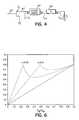
- FIG. 4is a block diagram illustrating output impedance characteristics of an amplifier.
- FIG. 5Ais a block diagram of an alternative embodiment of an amplifier circuit in accordance with the principles of the present invention.
- FIG. 5Bis a block diagram of another alternative embodiment of an amplifier circuit in accordance with the principles of the present invention.
- FIG. 6is a plot of amplifier efficiency for the embodiments of the present invention.
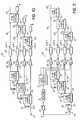
- FIG. 7is a block diagram of an alternative embodiment of an amplifier circuit in accordance with the principles of the present invention.
- FIG. 8is a block diagram of an alternative embodiment of an amplifier circuit in accordance with the principles of the present invention utilizing multiple auxiliary amplifiers.
- FIG. 9is a block diagram of another alternative embodiment of an amplifier circuit in accordance with the principles of the present invention utilizing multiple auxiliary amplifiers.
- FIG. 10is a block diagram of another alternative embodiment of an amplifier circuit in accordance with the principles of the present invention utilizing multiple auxiliary amplifiers.
- FIG. 11is a block diagram of another alternative embodiment of an amplifier circuit in accordance with the principles of the present invention utilizing multiple auxiliary amplifiers.
- FIG. 12is a block diagram of another alternative embodiment of an amplifier circuit in accordance with the principles of the present invention utilizing multiple auxiliary amplifiers.
- FIG. 13is a block diagram of another alternative embodiment of an amplifier circuit in accordance with the principles of the present invention utilizing multiple auxiliary amplifiers.
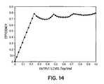
- FIG. 14is a graph of the efficiency of an embodiment of the present invention.
- the present inventionprovides a high efficiency amplifier architecture for efficiently handling high peak-to-average signal ratio applications.
- the amplifierdoes so, without complicated and expensive electronics and RF switches.
- the amplifieris viable with linearization schemes, including digital, analog, and hybrid pre-distortion, Feed Forward, and Cross Cancellation.
- itis compatible with drain bias modulation schemes.
- the present inventionprovides a new high efficiency power amplifier utilizing a load modulating scheme, like that of a classic Doherty amplifier, to improve amplifier efficiency when amplifying a signal with a high peak-to-average ratio. While utilizing some of the topology of a Doherty circuit in one embodiment of the invention, a new output topology is utilized to achieve the aspects of the present invention. To that end, some explanation of a classic Doherty circuit operation, which would be known to a person of ordinary skill in the art, is useful for understanding the operation of the present invention.
- a simple Doherty circuitwill combine the outputs of a main amplifier, such as a carrier amplifier and an auxiliary amplifier, such as a peaking amplifier.
- An input signal to the amplifiersis split, and the split signals are directed to the carrier amplifier and the peaking amplifier.
- the output of the carrier amplifieris combined through a quarter-wavelength impedance inverter with the output of the peaking amplifier, and the combined outputs are directed through a quarter-wavelength transformer to a load Z L .
- the output of the peaking amplifierelectrically acts like a current source and has a high output impedance.
- the output of the carrier amplifieracts like a current source and has a high output impedance until its output reaches saturation. After it reaches saturation, the output of the carrier or main amplifier looks like a voltage source and has low impedance.
- the peaking amplifierUnder a low input signal level drive condition, the peaking amplifier is turned OFF and its high output impedance is assumed to not significantly load the output circuit.
- the carrier amplifier's load impedanceis then approximately 2 Z L , which is approximately 2 ⁇ the nominal design level and, thus, the amplifier operates at a similar nominal efficiency.
- the peaking amplifierWhen the input signal drive level is increased to where the carrier amplifier reaches saturation, the peaking amplifier is allowed to turn ON, thus contributing current to the output circuit. The additional current causes the effective impedance inverter's output to increase which, in turn, results in a decreasing load impedance at the carrier amplifier's output.
- the carrier amplifierAs the input drive continues to rise, the carrier amplifier is kept in a voltage-saturated condition, but the power level of that saturated condition increases due to the decreasing load impedance.
- both the carrier and peaking amplifiershave their designated nominal load impedance, Z L , at their respective outputs, and are delivering their maximum rated power to the load.
- the present inventionwhile utilizing the combination of a main and an auxiliary amplifier, does not utilize separate quarter-wavelength transmission lines at the output to form an impedance inverter and an impedance transformer to combine the amplifier output signals. Rather, the present invention utilizes a hybrid coupler in the output transforming/combining circuitry. This is a distinctive difference from the prior art.
- the output couplerprovides significant advantages and is significantly simpler to implement than the classic Doherty design with quarter-wavelength lines.
- hybrid couplersare commercially available and can be surface-mounted on a printed circuit board. Since the surface-mounted hybrid couplers are typically implemented with higher dielectric constant materials, they can be physically smaller than quarter-wavelength transmission lines used in the classic Doherty design.
- hybrid couplerprovides for a wider bandwidth response for the amplifier than available with the classic Doherty circuit. Furthermore, use of the hybrid couplers allows the invention to be extended to low frequencies, which were difficult to implement with large quarter-wavelength transmission lines. Accordingly, the present invention provides significant benefits over the classic Doherty design.
- a hybrid coupler 10is illustrated as having port numbers 1 - 4 .
- ports 2 and 3might be considered input ports and ports 1 and 4 as output ports.
- the coupler's characteristic impedancesuch as, but not restricted to, 50 Ohms
- an input signalis applied to port 2
- a portion of the input signal's power P iappears at port 1
- the remaining portion of the input signal's powerappears at port 4 .
- little or no powerwould appear at the output of port 3 .
- the output signal portions at port 4will have a phase that is shifted ⁇ 90 degrees relative to the output signal portion at port 1 .
- a similar operationoccurs when port 2 is terminated and an input signal is applied to port 3 . Ideally, no power would appear at port 2 .
- the signal portion at port 1will have a phase that is shifted ⁇ 90 degrees relative to the output signal portion at port 4 .
- An example of a very common hybrid coupleris a ⁇ 3 dB hybrid coupler, which generally splits an input signal, such as at port 2 , equally between the output ports 1 and
- the hybrid coupler utilizedmay be implemented in many different ways.
- the hybrid coupler 10 in FIG. 1may be implemented utilizing transmission lines, coupled transmission lines, lumped element inductors and capacitors, and transformers.
- a coupled transmission line designis utilized for a coupler design in the >500 MHz region.
- the new systemdoes not preclude the use of other implementations.
- an implementation of the hybrid coupler for an HF, or VHF, high efficiency amplifiermay utilize a transformer.
- port 1 of the hybrid coupleris terminated in a short circuit and port 4 is terminated in a load impedance Z load , which could match the characteristic impedance of the coupler, for example.
- Port 2is left unterminated or as an open circuit. In such a case as illustrated in FIG. 2A , and where the coupler is a ⁇ 3 dB design, the input impedance Z i is equal to 2 Z load .
- amplifier 20includes a main amplifier input or primary amplifier input 26 and an amplifier output 28 . That is, an RF signal input at 26 is amplified and presented at output 28 to a load or effective load impedance Z load , although the amplifier output 28 may include combined amplified signals from the main amplifier circuit 22 and auxiliary amplifier circuit 24 in accordance with the invention.
- the input signal 26is divided between the main amplifier circuit 22 and auxiliary amplifier circuit 24 .
- an input hybrid coupler circuit 30is utilized for splitting the input signal 26 into individual signals or signal components 32 , 34 .
- Signal 32 from the splitting coupler 30is coupled as an input signal to main amplifier circuit 22
- signal 34is coupled as an input signal to auxiliary amplifier circuit 24 .
- the coupler circuit 30therefore acts as a splitting coupler circuit to split or divide the input signal 26 .
- the division ratio of the couplerdetermines the relative amplitude of signals 32 and 34 . This division ratio may be used to partially determine the selectively operable characteristics of the auxiliary amplifier.
- the hybrid coupler circuit 30is a ⁇ 3 dB hybrid coupler.
- the ⁇ 3 dB coupler circuit 30divides the input signal 26 into generally equal amplitude input signals 32 , 34 for the amplifier circuits 22 , 24 .
- the other input 36 of the coupler circuit 30is terminated through a suitable impedance such as a 50 Ohm resistor 38 to ground.
- the divided or split signalsare then amplified respectively by the main amplifier circuit 22 , or the main amplifier circuit in combination with the auxiliary amplifier 24 .
- the amplifier circuitsare also designated in the figures as “M” and “A” for “main” and “auxiliary ”.
- the auxiliary amplifier circuitis selectively operable to operate in combination with main amplifier circuit 22 when needed for peak power requirements or applications.
- the phasing lines 46 , 48are short lengths of transmission line, which have a selectable length and are used to present a desired characteristic impedance to the input of the coupler circuit 44 .
- the phasing lines 46 , 48are selected to operate in conjunction with any output matching circuitry of the amplifier circuits, as discussed below, to maximize or minimize the effective amplifier output impedance Z out , depending on the hybrid coupler configuration to be used.
- the auxiliary amplifier circuit 24is selectively operable to be turned ON and OFF as needed to handle power requirements.
- the main amplifier 22might also be selectively operable to turn it OFF.
- FIG. 3Ais reflective of a hybrid coupler configuration, as illustrated in FIG. 2A wherein output port 1 is terminated in a short using an open circuit transmission line 50 to reflect an electrical short to port 1 of the hybrid coupler circuit 44 .
- an effective short circuitmight be physically located directly adjacent to port 1 of the hybrid coupler, similar to the configuration as illustrated in FIG. 2 A.
- the transmission line section 50such as a quarter-wavelength (90 degree) transmission line will allow the termination, whether a short or open circuit, to be moved away from the coupler port.
- the length of the open circuit transmission line 50is selected to reflect one of an electrical short or an electrical open circuit at output port 1 .
- FIG. 3Billustrates an alternative embodiment of the invention, wherein an open circuit is used for the termination of port 1 , such as wherein a length of transmission line 50 is selected with a short at one end to reflect an open circuit to the hybrid coupler circuit 44 .
- like componentsare given similar reference numerals.
- the position of the main (M) amplifier circuit, or carrier amplifier 22 and the position of the auxiliary (A) amplifier circuit, or peaking amplifier 24are reversed with respect to the embodiment as illustrated in FIG. 3 A.
- the auxiliary amplifier circuit 24is selectively turned ON and OFF as needed for peak power requirements. As such, there may be a significant amount of time in which only the main amplifier circuit 22 is operating.
- the present inventionwith a short or open circuit presented to the port 1 of the coupler, provides significant advantages to simply terminating the port with the characteristic impedance of the coupler. In a hybrid coupler having one output port (e.g. port 1 ) terminated through a characteristic impedance, such as a 50 Ohm resistor to ground, a 6 db power loss would be realized when the auxiliary amplifier circuit is OFF.
- the length of the transmission line, 50are selected so that an electrical short or an electrical open circuit is reflected back into the coupler circuit 44 .
- the characteristics of the transmission linemay essentially remain set as tuned. Therefore, if the length or width of the transmission line 50 is varied to change its electrical length or impedance characteristics, it may remain at the selected length or width regardless of whether the auxiliary amplifier circuit 24 is ON or OFF.
- the transmission line 50might have a selectable effective length and effective impedance characteristic for possibly dynamically varying its effect on the circuit of the invention, although such dynamic adjustments may not be necessary.
- both the main amplifier and auxiliary amplifier output impedancesneed to be high, such that they act as current sources.
- the final stage deviceusually a transistor, is followed by a matching network that transforms a convenient impedance level at the amplifier output (usually, but not restricted to, 50 Ohms) to a less convenient impedance level (perhaps, on the order of 2 Ohms), at the transistor terminals.
- the output matching network 64causes an impedance inversion, it is necessary to load the amplifier circuit with an impedance that is lower than the nominal design level (i.e. ⁇ Z L ) to have the amplifier operate in a more efficient mode. It should also be noted that, in this mode of the operation, the gain of the amplifier increases with decreasing load impedance. Such a condition is reflective of an inverted mode of a Doherty amplifier operation. In the present invention, and again referring to FIG. 4 , the output impedance Z out will not be at the maximum possible value when a high Z out is desired. Similarly, the output impedance will not be at a minimum when a low Z out is desired.
- a short length of transmission line 66is selected, having a characteristic impedance Z L .
- the length of transmission line 66is coupled between the output matching circuit and the load Z L , as shown in FIG. 4 .
- the phasing line 66is selected to maximize or minimize Z out ′, depending upon the configuration of the amplifier to be utilized in the position of the main amplifier circuit and the auxiliary amplifier circuit.
- FIGS. 5A and 5Billustrate basic configurations of the high efficiency amplifier of the invention when operating in the inverted mode, i.e. when the transistor output has high impedance and the output matching network causes an impedance inversion, such that the output impedance is low.
- FIGS. 5A and 5Bthey are similar to the configurations as utilized in FIGS. 3A and 3B , but the physical location of the main (M) amplifier circuit (carrier amplifier) and auxiliary (A) amplifier circuit (peaking amplifier) are reversed from their positions illustrated in FIGS. 3A and 3B .
- the carrier amplifier loadis C 2 Z L , which is lower than the nominal design value of Z L .
- the choice of the mode of operationis best determined after the peaking and carrier amplifier matching circuit designs are complete.
- the resultant amplifier impedancesare high, those topologies illustrated in FIGS. 3A and 3B are preferable.
- the resultant amplifier impedancesare low, those topologies illustrated in FIGS. 5A and 5B are preferable.
- main amplifier circuits and auxiliary amplifier circuits with generally equal power output capabilities, or power ratingsare utilized.
- the hybrid couplers 44 utilizing the outputmay be ⁇ 3 dB hybrid couplers, which are suitable for amplifiers with equal output power ratings.
- the auxiliary amplifiermight be rated at twice the output power of the carrier amplifier.
- the design of the couplermay be selected to address any differences between the output power ratings of the various amplifier components.
- a ⁇ 4.77 dB designmay be utilized for an auxiliary amplifier rated at twice the output power of the main amplifier.
- the choice of input coupler value for the combining hybrid coupler 44depends upon the relative gains of the main and auxiliary amplifiers.
- the various configurations shown in the Figures hereincan be designed to operate with any ratio of auxiliary amplifier to main amplifier power ratings.
- the output power at which the amplifier reaches its first efficiency peakwill decrease.
- the plot in FIG. 6indicates this effect.
- the gate control circuit 70is operated to control the turn ON characteristics of the auxiliary amplifier circuit 24 .
- the gate (or base or grid) biasesare modulated to thereby control the TURN ON characteristics.
- Various different techniques for such gate bias modulation and gate controlare known to those skilled in the art and such appropriate techniques may be utilized. This allows the auxiliary amplifier 24 to remain turned OFF until a higher input signal level is reached, while still allowing the auxiliary amplifier to reach its full output capability at the peak input signal level.
- the use of gate controlmay be used with any of the disclosed embodiments.
- An input signal 26is input to the hybrid coupler circuits, and is directed on a path to coupler circuits 110 , 114 , 118 , which further split the signal.
- Signal 26is directed to a first hybrid coupler, such as a ⁇ 6 dB hybrid coupler circuit 110 .
- One output signal 111 from an output port of hybrid coupler circuit 110is directed to auxiliary amplifier 108 , while another output 112 is directed to a second hybrid coupler circuit 114 , which may be a ⁇ 4.77 dB coupler.
- the coupling value of the various couplersmay vary based upon the serial feed arrangement in order to input generally equal signals to the various main and auxiliary amplifier circuits 102 - 108 .
- the arrangement shown in FIGS. 8 and 9assumes generally equal power output capabilities for the main and auxiliary amplifiers. Alternatively, different sized amplifiers might be used and the coupler values adjusted accordingly to adapt to unequal power ratings for the amplifiers.
- Coupler circuit 118may be a ⁇ 3 dB coupler with its respective outputs 119 , 120 being directed to the auxiliary amplifier 104 and the main amplifier 102 , respectively.
- a serial arrangement to divide the input signal among the various amplifier circuits 102 - 108is reflective of the serial combiner arrangement utilized at the output, as discussed further below.
- the output signals of the main and auxiliary amplifier circuits 102 - 108are coupled through phasing lines 130 to coupler circuits 132 , 134 , 142 arranged in a serial combiner arrangement.
- the outputs of auxiliary amplifiers 106 , 108are directed to coupler circuit 132 , such as a ⁇ 3 dB coupler.
- coupler circuit 132such as a ⁇ 3 dB coupler.
- One output signal 136 of the coupler circuit 132is directed to another hybrid coupler circuit 134 , while the other output port is coupled to a tuned transmission line 135 , which is tuned to reflect an electrical short to the coupler circuit, as discussed above.
- the other output 136is combined with an output 138 from auxiliary amplifier circuit 104 .
- Coupler circuit 134which may be a ⁇ 4.77 dB coupler circuit, has one output port coupled to a tuned transmission line 138 , while the other output 140 is fed to a hybrid coupler circuit 142 , where it is combined with the output 143 from the main amplifier circuit 102 .
- Coupler circuit 142may be a ⁇ 6 dB coupler as illustrated.
- a tuned, open-circuited transmission line 144is coupled with an output port of the coupler circuit 142 to reflect a short to that port.
- the other output 145is reflective of the combined output from the various amplifiers and coupler circuits, and provides the output of amplifier 100 .
- main amplifier circuit 102might be on while, in sequence, the auxiliary amplifier circuits 104 , 106 , 108 are turned ON according to the level of the input signal.
- the phasing lines in FIGS. 8 and 9are selected so that the maximum output impedance is presented to the inputs of couplers 132 , 134 , and 142 .
- FIG. 8might also be utilized with gate control as illustrated in FIG. 9 , wherein like reference numerals are utilized to illustrate the gate control circuitry as in FIG. 7 .
- the coupler circuit 76couples off a portion of the signal 79 , which is directed to appropriate gate controlled circuit 70 through an attenuator 74 and a detector 72 . Outputs of the gate controlled circuit are coupled appropriately to the turn ON characteristic of the auxiliary amplifier circuits.
- FIGS. 10 and 11show multiple amplifiers having low impedance characteristics, such as “inverted mode” characteristics and with and without gate control, respectively.
- various main and auxiliary amplifiers 102 - 108in combination with their respective phasing lines, will reflect a low output impedance at the input ports of the couplers. While the phasing lines 130 are given common reference numerals between each of the amplifiers, that does not indicate that such phasing lines will have generally the same length. Rather, the lengths of the phasing lines are shown to maximize or, as in the case of FIGS. 10 and 11 , minimize the output impedance (see FIG. 4 ).
- the main amplifier and auxiliary amplifiersare arranged as set forth in FIGS.
- FIGS. 10 and 11illustrate an inverted-mode operation of a multiple amplifier circuit
- phasing transmission lines 130are set so that a low impedance is presented to input ports of the various hybrid coupler circuits 132 , 134 , and 142 .
- open circuitsare presented at the isolated ports of the output couplers. While FIG. 10 illustrates a length of transmission line terminated in a short, might be utilized to reflect an open circuit and move the termination away from the coupler, a single open circuit at the output ports might also be utilized.
- FIG. 11is similar to FIG. 10 and illustrates utilization of a gate controlled circuit for controlling the turn-ON bias for the auxiliary amplifiers.
- the power output capability of the amplifiersmay be equal or unequal.
- the hybrid coupler circuits and their coupling valuesmay be chosen to reflect the relative amplifier power output capabilities.
- a ⁇ 3 dB hybrid couplermay be suitable for main and auxiliary amplifiers with generally equal power output capabilities.
- Different coupler values, such as a ⁇ 4.77 coupler,may be utilized for those situations in which the main and auxiliary amplifiers have unequal power capabilities.
- FIGS. 8-11are shown with a serial signal feed to the amplifiers.
- a corporate or parallel feed arrangementmight be used.
- an amplifier 160is illustrated, having a main amplifier circuit 162 and auxiliary amplifier circuits 164 , 166 , 168 .
- the amplifier circuitsare fed by a parallel or corporate signal divider arrangement, incorporating coupler circuits 170 , 172 , which may be ⁇ 3 dB hybrid coupler circuits.
- the plurality of amplifier circuits 162 - 168are fed in a corporate arrangement and thus require multiple stages of hybrid coupler circuits. Therefore, a hybrid coupler circuit 174 is utilized to divide the incoming input signal generally equally between the coupler circuits 170 , 172 , which then feed the amplifier circuits. Like numerals are utilized in FIGS. 12 and 13 for similar signal and circuit components, as discussed herein above with respect to other Figures.
- the input coupler circuits, or splitting coupler circuits 170 , 172 , 174have one input terminated through a 50 Ohm resistor 38 to ground.
- the auxiliary amplifier circuits 164 , 166 , 168are coupled to hybrid coupler circuits 182 , 184 , 186 to combine their various outputs to a single RF output 118 .
- the outputs of main amplifier circuit 162 and auxiliary amplifier circuit 164are coupled through appropriate phasing lines 180 to respective coupler circuit 182 .
- the auxiliary amplifiers 166 , 168are coupled through phasing lines 180 to a respective coupler circuit 184 .
- the outputs from the coupler circuits 182 , 184are then combined through another coupler circuit 186 to form output signal 118 .
- the coupler circuits 182 , 184 , 186may be ⁇ 3 dB hybrid couplers as illustrated or some other suitable coupler circuit.
- the coupler circuitsare arranged in a corporate combiner arrangement.
- one of the outputs of each coupler circuitis the combined signal from the amplifier circuits or other components connected thereto.
- the other coupler output portis coupled to one of a short or open circuit, such as through a transmission line segment.
- coupler circuit 182has a first coupler output 188 which combines the amplifier output signals from amplifier circuits 162 , 164 and passes them through to the coupler circuit 186 .
- a phasing line 190is utilized between coupler circuit 182 and coupler circuit 186 .
- phasing line 190may be utilized for the coupler circuit 184 and the output 188 thereof, which is reflective of the amplifier circuits 166 , 168 .
- the other coupler output 192 of each of the coupler circuits 182 , 184feeds to an open-circuit tuned transmission line 194 , which is selected so that an electrical short is reflected back into the coupler circuits 182 , 184 respectively.
- the length of the open-circuit transmission line 194will be determined and set for a specific amplifier circuit and respective coupler circuit and will remain tuned.
- the coupler circuit 186is terminated by an open-circuit tuned transmission line 196 , which is tuned for reflecting an open circuit back to the output port of the coupler circuit 186 . Therefore, in accordance with the principles of the present invention, the outputs of the amplifier circuits are combined efficiently so that the auxiliary amplifier circuits may be selectively operated to provide a peak power output for the amplifier 160 .
- gate control circuit 70may be operated to selectively turn ON the auxiliary amplifier circuits 164 - 168 as desired when signal peaks are detected by the detector 72 .
- main amplifier 162may be ON and auxiliary amplifier 168 may be turned ON when a specific signal level is detected.
- the gate control circuit 70controls the turn ON characteristics of the auxiliary amplifier 168 .
- the gate control circuit 70may be utilized to turn ON other auxiliary amplifier circuits, such as circuits 164 and 166 .
- the coupler circuits 182 , 184 , and 186combine the signals from the main and the auxiliary amplifier circuits into a single output 118 for the amplifier 160 .
- FIG. 14depicts the efficiency characteristics that may be obtained with a system similar to that illustrated in FIG. 8 , for example.
- the multiple amplifier systemoffers a better efficiency over a wider range of signal amplitudes than is generally obtained with a two-amplifier system (compare with FIG. 6 ).
- the present inventionis utilized to improve the efficiency performance for amplifier applications requiring high peak-to-average characteristics.
- the inventionis viable with various linearization schemes, including digital, analog, and hybrid Pre-distortion, Feed Forward and Cross Cancellation. It is also compatible with drain biased modulation schemes.
Landscapes
- Engineering & Computer Science (AREA)
- Power Engineering (AREA)
- Amplifiers (AREA)
- Microwave Amplifiers (AREA)
Abstract
Description
Claims (39)
Priority Applications (8)
| Application Number | Priority Date | Filing Date | Title |
|---|---|---|---|
| US10/402,800US6922102B2 (en) | 2003-03-28 | 2003-03-28 | High efficiency amplifier |
| US10/795,055US7064606B2 (en) | 2003-03-28 | 2004-03-05 | High efficiency amplifier and method of designing same |
| KR1020057017835AKR101123505B1 (en) | 2003-03-28 | 2004-03-26 | High efficiency amplifier and method of designing same |
| JP2006509330AJP4870556B2 (en) | 2003-03-28 | 2004-03-26 | High efficiency amplifier and design method thereof |
| EP04758381AEP1609239B1 (en) | 2003-03-28 | 2004-03-26 | High efficiency amplifier and method of designing same |
| PCT/US2004/009265WO2004088837A2 (en) | 2003-03-28 | 2004-03-26 | Doherty amplifier with output hybrid coupler |
| DE602004028227TDE602004028227D1 (en) | 2003-03-28 | 2004-03-26 | HIGHLY EFFICIENT AMPLIFIER AND METHOD FOR ITS DESIGN |
| CN2004800142647ACN1833358B (en) | 2003-03-28 | 2004-03-26 | Doherty amplifier with output mixing coupler |
Applications Claiming Priority (1)
| Application Number | Priority Date | Filing Date | Title |
|---|---|---|---|
| US10/402,800US6922102B2 (en) | 2003-03-28 | 2003-03-28 | High efficiency amplifier |
Related Child Applications (1)
| Application Number | Title | Priority Date | Filing Date |
|---|---|---|---|
| US10/795,055Continuation-In-PartUS7064606B2 (en) | 2003-03-28 | 2004-03-05 | High efficiency amplifier and method of designing same |
Publications (2)
| Publication Number | Publication Date |
|---|---|
| US20040189380A1 US20040189380A1 (en) | 2004-09-30 |
| US6922102B2true US6922102B2 (en) | 2005-07-26 |
Family
ID=32989816
Family Applications (2)
| Application Number | Title | Priority Date | Filing Date |
|---|---|---|---|
| US10/402,800Expired - LifetimeUS6922102B2 (en) | 2003-03-28 | 2003-03-28 | High efficiency amplifier |
| US10/795,055Expired - LifetimeUS7064606B2 (en) | 2003-03-28 | 2004-03-05 | High efficiency amplifier and method of designing same |
Family Applications After (1)
| Application Number | Title | Priority Date | Filing Date |
|---|---|---|---|
| US10/795,055Expired - LifetimeUS7064606B2 (en) | 2003-03-28 | 2004-03-05 | High efficiency amplifier and method of designing same |
Country Status (4)
| Country | Link |
|---|---|
| US (2) | US6922102B2 (en) |
| JP (1) | JP4870556B2 (en) |
| CN (1) | CN1833358B (en) |
| DE (1) | DE602004028227D1 (en) |
Cited By (15)
| Publication number | Priority date | Publication date | Assignee | Title |
|---|---|---|---|---|
| US20050212078A1 (en)* | 2004-03-24 | 2005-09-29 | Youngwoo Kwon | Integrated circuit module package and assembly method thereof |
| US20060109053A1 (en)* | 2004-11-25 | 2006-05-25 | Wavics Inc. | Series-Type Doherty Amplifier Without Hybrid Coupler |
| US20060244524A1 (en)* | 2005-04-27 | 2006-11-02 | Korea Advanced Institute Of Science And Technology | Power amplifier with automatic switching function |
| US20070098109A1 (en)* | 2003-08-07 | 2007-05-03 | Venkatesh Vadde | Method and apparatus for discrete power synthesis of multicarrier signals with constant envelope power amplifiers |
| US20070126502A1 (en)* | 2005-12-01 | 2007-06-07 | Louis Edward V | High gain, high efficiency power amplifier |
| US20080088369A1 (en)* | 2006-09-29 | 2008-04-17 | Gregory Bowles | Enhanced doherty amplifier with asymmetrical semiconductors |
| US20080122542A1 (en)* | 2006-11-27 | 2008-05-29 | Gregory Bowles | Enhanced amplifier with auxiliary path bias modulation |
| US20090154544A1 (en)* | 2007-12-18 | 2009-06-18 | Infineon Technologies Ag | Amplifier Modulation Method and Apparatus |
| US20090278599A1 (en)* | 2008-05-09 | 2009-11-12 | Cree, Inc. | Progressive power generating amplifiers |
| US7934190B1 (en) | 2008-09-25 | 2011-04-26 | The United States Of America As Represented By The Secretary Of The Navy | Multiple amplifier matching over lumped networks of arbitrary topology |
| US8461938B2 (en)* | 2010-10-29 | 2013-06-11 | Freescale Semiconductor, Inc. | Directional couplers for use in electronic devices, and methods of use thereof |
| US8593219B1 (en) | 2012-08-31 | 2013-11-26 | Motorola Solutions, Inc. | Method and apparatus for amplifying a radio frequency signal |
| US8860529B2 (en) | 2010-09-10 | 2014-10-14 | Anaren, Inc. | Impedance transforming coupler |
| US9484613B1 (en)* | 2010-01-29 | 2016-11-01 | United States Of America As Represented By The Administrator Of National Aeronautics And Space Administration | Ka-band waveguide 2-way hybrid combiner for MMIC amplifiers with unequal and arbitrary power output ratio |
| WO2024153329A1 (en) | 2023-01-19 | 2024-07-25 | Telefonaktiebolaget Lm Ericsson (Publ) | Combination of balanced amplifiers for resilience to load impedance variation |
Families Citing this family (142)
| Publication number | Priority date | Publication date | Assignee | Title |
|---|---|---|---|---|
| KR100553252B1 (en)* | 2002-02-01 | 2006-02-20 | 아바고테크놀로지스코리아 주식회사 | Power amplifier of portable terminal |
| US8811917B2 (en)* | 2002-05-01 | 2014-08-19 | Dali Systems Co. Ltd. | Digital hybrid mode power amplifier system |
| US8472897B1 (en) | 2006-12-22 | 2013-06-25 | Dali Systems Co. Ltd. | Power amplifier predistortion methods and apparatus |
| US6985704B2 (en) | 2002-05-01 | 2006-01-10 | Dali Yang | System and method for digital memorized predistortion for wireless communication |
| US8380143B2 (en) | 2002-05-01 | 2013-02-19 | Dali Systems Co. Ltd | Power amplifier time-delay invariant predistortion methods and apparatus |
| US7254449B2 (en)* | 2002-07-31 | 2007-08-07 | Advanced Bionics Corp | Systems and methods for providing power to one or more implantable devices |
| US7279971B2 (en)* | 2002-09-06 | 2007-10-09 | Telefonaktiebolaget Lm Ericsson (Publ) | Composite power amplifier |
| US7275292B2 (en) | 2003-03-07 | 2007-10-02 | Avago Technologies Wireless Ip (Singapore) Pte. Ltd. | Method for fabricating an acoustical resonator on a substrate |
| US7388454B2 (en) | 2004-10-01 | 2008-06-17 | Avago Technologies Wireless Ip Pte Ltd | Acoustic resonator performance enhancement using alternating frame structure |
| US7355470B2 (en) | 2006-04-24 | 2008-04-08 | Parkervision, Inc. | Systems and methods of RF power transmission, modulation, and amplification, including embodiments for amplifier class transitioning |
| US7327803B2 (en) | 2004-10-22 | 2008-02-05 | Parkervision, Inc. | Systems and methods for vector power amplification |
| US7148746B2 (en) | 2004-10-26 | 2006-12-12 | Andrew Corporation | High efficiency amplifier |
| US8981876B2 (en) | 2004-11-15 | 2015-03-17 | Avago Technologies General Ip (Singapore) Pte. Ltd. | Piezoelectric resonator structures and electrical filters having frame elements |
| US7202560B2 (en) | 2004-12-15 | 2007-04-10 | Avago Technologies Wireless Ip (Singapore) Pte. Ltd. | Wafer bonding of micro-electro mechanical systems to active circuitry |
| US7791434B2 (en) | 2004-12-22 | 2010-09-07 | Avago Technologies Wireless Ip (Singapore) Pte. Ltd. | Acoustic resonator performance enhancement using selective metal etch and having a trench in the piezoelectric |
| US7138861B2 (en)* | 2004-12-29 | 2006-11-21 | Telefonaktiebolaget L M Ericsson (Publ) | Load mismatch adaptation in coupler-based amplifiers |
| US7369013B2 (en) | 2005-04-06 | 2008-05-06 | Avago Technologies Wireless Ip Pte Ltd | Acoustic resonator performance enhancement using filled recessed region |
| US7868522B2 (en)* | 2005-09-09 | 2011-01-11 | Avago Technologies Wireless Ip (Singapore) Pte. Ltd. | Adjusted frequency temperature coefficient resonator |
| US7737807B2 (en)* | 2005-10-18 | 2010-06-15 | Avago Technologies Wireless Ip (Singapore) Pte. Ltd. | Acoustic galvanic isolator incorporating series-connected decoupled stacked bulk acoustic resonators |
| US7675390B2 (en) | 2005-10-18 | 2010-03-09 | Avago Technologies Wireless Ip (Singapore) Pte. Ltd. | Acoustic galvanic isolator incorporating single decoupled stacked bulk acoustic resonator |
| US7911272B2 (en) | 2007-06-19 | 2011-03-22 | Parkervision, Inc. | Systems and methods of RF power transmission, modulation, and amplification, including blended control embodiments |
| US8334722B2 (en) | 2007-06-28 | 2012-12-18 | Parkervision, Inc. | Systems and methods of RF power transmission, modulation and amplification |
| US9106316B2 (en) | 2005-10-24 | 2015-08-11 | Parkervision, Inc. | Systems and methods of RF power transmission, modulation, and amplification |
| US20130078934A1 (en) | 2011-04-08 | 2013-03-28 | Gregory Rawlins | Systems and Methods of RF Power Transmission, Modulation, and Amplification |
| US7463499B2 (en) | 2005-10-31 | 2008-12-09 | Avago Technologies General Ip (Singapore) Pte Ltd. | AC-DC power converter |
| WO2007077409A1 (en)* | 2006-01-05 | 2007-07-12 | Filtronic Plc | An active load pull amplifier |
| US7612636B2 (en) | 2006-01-30 | 2009-11-03 | Avago Technologies Wireless Ip (Singapore) Pte. Ltd. | Impedance transforming bulk acoustic wave baluns |
| US20070210748A1 (en)* | 2006-03-09 | 2007-09-13 | Mark Unkrich | Power supply and electronic device having integrated power supply |
| US7746677B2 (en)* | 2006-03-09 | 2010-06-29 | Avago Technologies Wireless Ip (Singapore) Pte. Ltd. | AC-DC converter circuit and power supply |
| US7479685B2 (en) | 2006-03-10 | 2009-01-20 | Avago Technologies General Ip (Singapore) Pte. Ltd. | Electronic device on substrate with cavity and mitigated parasitic leakage path |
| US8031804B2 (en) | 2006-04-24 | 2011-10-04 | Parkervision, Inc. | Systems and methods of RF tower transmission, modulation, and amplification, including embodiments for compensating for waveform distortion |
| US7937106B2 (en) | 2006-04-24 | 2011-05-03 | ParkerVision, Inc, | Systems and methods of RF power transmission, modulation, and amplification, including architectural embodiments of same |
| CN101479956B (en)* | 2006-04-28 | 2013-07-31 | 大力系统有限公司 | High Efficiency Linearized Power Amplifier for Wireless Communications |
| US20070280377A1 (en)* | 2006-06-02 | 2007-12-06 | Rucki John S | Apparatus and method for controlling the output power of a transmitter using a pilot channel power level |
| US7486136B2 (en)* | 2006-09-26 | 2009-02-03 | Infineon Technologies Ag | Power amplifier |
| DE102006052611A1 (en)* | 2006-11-08 | 2008-05-15 | Eads Deutschland Gmbh | Linear broadband amplifier e.g. measuring amplifier, for measuring techniques, has amplifier stages connected in parallel between hybrid couplers, where stages are based on transistors made of semiconductor materials with large band gaps |
| JPWO2008075561A1 (en)* | 2006-12-19 | 2010-04-08 | 三菱電機株式会社 | Power amplifier |
| WO2008079391A1 (en)* | 2006-12-22 | 2008-07-03 | Arizona Board Of Regents For And On Behalf Of Asu | Resonant linearly polarized eddy current sensor |
| US9026067B2 (en)* | 2007-04-23 | 2015-05-05 | Dali Systems Co. Ltd. | Remotely reconfigurable power amplifier system and method |
| CN102017553B (en) | 2006-12-26 | 2014-10-15 | 大力系统有限公司 | Method and system for baseband predistortion linearization in a multi-channel broadband communication system |
| US7620129B2 (en) | 2007-01-16 | 2009-11-17 | Parkervision, Inc. | RF power transmission, modulation, and amplification, including embodiments for generating vector modulation control signals |
| KR101484796B1 (en)* | 2007-04-23 | 2015-01-20 | 달리 시스템즈 씨오. 엘티디. | N-way doherty distributed power amplifier |
| US8274332B2 (en) | 2007-04-23 | 2012-09-25 | Dali Systems Co. Ltd. | N-way Doherty distributed power amplifier with power tracking |
| WO2008144017A1 (en) | 2007-05-18 | 2008-11-27 | Parkervision, Inc. | Systems and methods of rf power transmission, modulation, and amplification |
| US7474156B2 (en)* | 2007-05-25 | 2009-01-06 | Avago Technologies Wireless Ip (Singapore) Pte. Ltd. | Impedance transformer for amplifier and amplifier including the same |
| WO2008156800A1 (en) | 2007-06-19 | 2008-12-24 | Parkervision, Inc. | Combiner-less multiple input single output (miso) amplification with blended control |
| US8224266B2 (en)* | 2007-08-30 | 2012-07-17 | Dali Systems Co., Ltd. | Power amplifier predistortion methods and apparatus using envelope and phase detector |
| US20090079514A1 (en)* | 2007-09-24 | 2009-03-26 | Tiberiu Jamneala | Hybrid acoustic resonator-based filters |
| US7791435B2 (en) | 2007-09-28 | 2010-09-07 | Avago Technologies Wireless Ip (Singapore) Pte. Ltd. | Single stack coupled resonators having differential output |
| US8384475B2 (en)* | 2007-11-19 | 2013-02-26 | Telefonaktiebolaget Lm Ericsson (Publ) | Composite amplifier, a radio terminal and a method for improving the efficiency of the composite amplifier |
| CN102150361B (en) | 2007-12-07 | 2016-11-09 | 大力系统有限公司 | Baseband-derived RF digital predistortion |
| TW200926576A (en)* | 2007-12-10 | 2009-06-16 | Wistron Neweb Corp | Down-converter having matching circuits with tuning mechanism coupled to 90 degree hybrid coupler included therein |
| JP5246257B2 (en)* | 2008-04-24 | 2013-07-24 | 日本電気株式会社 | amplifier |
| US7732977B2 (en) | 2008-04-30 | 2010-06-08 | Avago Technologies Wireless Ip (Singapore) | Transceiver circuit for film bulk acoustic resonator (FBAR) transducers |
| US7855618B2 (en) | 2008-04-30 | 2010-12-21 | Avago Technologies Wireless Ip (Singapore) Pte. Ltd. | Bulk acoustic resonator electrical impedance transformers |
| CN101567665B (en)* | 2008-12-26 | 2012-01-25 | 芯通科技(成都)有限公司 | Digital Doherty power amplifier |
| CN101534093B (en) | 2009-04-14 | 2011-08-10 | 武汉正维电子技术有限公司 | Final three-route power synthesizing amplifying circuit applied to power amplifier of mobile communication base station system |
| US8902023B2 (en) | 2009-06-24 | 2014-12-02 | Avago Technologies General Ip (Singapore) Pte. Ltd. | Acoustic resonator structure having an electrode with a cantilevered portion |
| US8248185B2 (en) | 2009-06-24 | 2012-08-21 | Avago Technologies Wireless Ip (Singapore) Pte. Ltd. | Acoustic resonator structure comprising a bridge |
| US8193877B2 (en) | 2009-11-30 | 2012-06-05 | Avago Technologies Wireless Ip (Singapore) Pte. Ltd. | Duplexer with negative phase shifting circuit |
| EP2339746B1 (en)* | 2009-12-15 | 2013-02-20 | Nxp B.V. | Doherty amplifier with composed transfer characteristic having multiple peak amplifiers |
| US9243316B2 (en) | 2010-01-22 | 2016-01-26 | Avago Technologies General Ip (Singapore) Pte. Ltd. | Method of fabricating piezoelectric material with selected c-axis orientation |
| US8796904B2 (en) | 2011-10-31 | 2014-08-05 | Avago Technologies General Ip (Singapore) Pte. Ltd. | Bulk acoustic resonator comprising piezoelectric layer and inverse piezoelectric layer |
| EP3376667B1 (en) | 2010-04-19 | 2021-07-28 | Qorvo US, Inc. | Pseudo-envelope following power management system |
| CN103597807B (en) | 2010-09-14 | 2015-09-30 | 大理系统有限公司 | Remotely reconfigurable distributed antenna system and method |
| WO2012047738A1 (en) | 2010-09-29 | 2012-04-12 | Rf Micro Devices, Inc. | SINGLE μC-BUCKBOOST CONVERTER WITH MULTIPLE REGULATED SUPPLY OUTPUTS |
| CN102142812B (en)* | 2010-12-17 | 2013-08-28 | 华为技术有限公司 | Doherty power amplifier |
| US8962443B2 (en) | 2011-01-31 | 2015-02-24 | Avago Technologies General Ip (Singapore) Pte. Ltd. | Semiconductor device having an airbridge and method of fabricating the same |
| KR101373769B1 (en) | 2011-02-15 | 2014-03-14 | 성균관대학교산학협력단 | Apparatus and method for high efficiency variable power transmission |
| KR101145666B1 (en)* | 2011-02-24 | 2012-05-25 | 포항공과대학교 산학협력단 | Three-stage gan hemt doherty power amplifier for high frequency applications |
| US9048812B2 (en) | 2011-02-28 | 2015-06-02 | Avago Technologies General Ip (Singapore) Pte. Ltd. | Bulk acoustic wave resonator comprising bridge formed within piezoelectric layer |
| US9203374B2 (en) | 2011-02-28 | 2015-12-01 | Avago Technologies General Ip (Singapore) Pte. Ltd. | Film bulk acoustic resonator comprising a bridge |
| US9083302B2 (en) | 2011-02-28 | 2015-07-14 | Avago Technologies General Ip (Singapore) Pte. Ltd. | Stacked bulk acoustic resonator comprising a bridge and an acoustic reflector along a perimeter of the resonator |
| US9425764B2 (en) | 2012-10-25 | 2016-08-23 | Avago Technologies General Ip (Singapore) Pte. Ltd. | Accoustic resonator having composite electrodes with integrated lateral features |
| US9136818B2 (en) | 2011-02-28 | 2015-09-15 | Avago Technologies General Ip (Singapore) Pte. Ltd. | Stacked acoustic resonator comprising a bridge |
| US9148117B2 (en) | 2011-02-28 | 2015-09-29 | Avago Technologies General Ip (Singapore) Pte. Ltd. | Coupled resonator filter comprising a bridge and frame elements |
| US9154112B2 (en) | 2011-02-28 | 2015-10-06 | Avago Technologies General Ip (Singapore) Pte. Ltd. | Coupled resonator filter comprising a bridge |
| US9444426B2 (en) | 2012-10-25 | 2016-09-13 | Avago Technologies General Ip (Singapore) Pte. Ltd. | Accoustic resonator having integrated lateral feature and temperature compensation feature |
| US8575820B2 (en) | 2011-03-29 | 2013-11-05 | Avago Technologies General Ip (Singapore) Pte. Ltd. | Stacked bulk acoustic resonator |
| JP5678768B2 (en)* | 2011-03-30 | 2015-03-04 | 日本電気株式会社 | Amplifier |
| DE102011075312A1 (en)* | 2011-05-05 | 2012-11-08 | Rohde & Schwarz Gmbh & Co. Kg | Quasi-broadband Doherty amplifier and related capacitor circuit |
| KR20140034895A (en) | 2011-06-02 | 2014-03-20 | 파커비전, 인크. | Antenna control |
| US8350445B1 (en) | 2011-06-16 | 2013-01-08 | Avago Technologies Wireless Ip (Singapore) Pte. Ltd. | Bulk acoustic resonator comprising non-piezoelectric layer and bridge |
| CN102355198B (en)* | 2011-08-01 | 2013-11-27 | 深圳大学 | Multi-channel Asymmetrical Doherty Power Amplifier |
| US8922302B2 (en) | 2011-08-24 | 2014-12-30 | Avago Technologies General Ip (Singapore) Pte. Ltd. | Acoustic resonator formed on a pedestal |
| US8698557B2 (en)* | 2011-10-12 | 2014-04-15 | Hbc Solutions, Inc. | Hybrid coupler |
| US8718580B2 (en) | 2011-11-11 | 2014-05-06 | Hbc Solutions, Inc. | Broadband high efficiency amplifier system incorporating dynamic modulation of load impedance |
| US8670732B2 (en) | 2011-11-11 | 2014-03-11 | Hbc Solutions, Inc. | Broadband amplifier system using a 3dB quadrature combiner to dynamically modulate load impedance |
| US9813036B2 (en)* | 2011-12-16 | 2017-11-07 | Qorvo Us, Inc. | Dynamic loadline power amplifier with baseband linearization |
| JP5799858B2 (en) | 2012-03-05 | 2015-10-28 | 富士通株式会社 | Amplifier |
| US8970297B2 (en)* | 2012-03-19 | 2015-03-03 | Qualcomm Incorporated | Reconfigurable input power distribution doherty amplifier with improved efficiency |
| US20130241656A1 (en) | 2012-03-19 | 2013-09-19 | Auriga Measurement Systems, LLC | Power Amplification System Using Doherty Amplifier with Linearization Circuit and Related Techniques |
| DE102012211308A1 (en)* | 2012-06-29 | 2014-04-03 | Rohde & Schwarz Gmbh & Co. Kg | Quasi-broadband amplifier according to the Doherty principle |
| US9219444B2 (en) | 2012-08-02 | 2015-12-22 | Imagine Communications Corp. | Broadband high efficiency amplifier system and a method of constructing high power amplitude modulated RF signal |
| US8742842B2 (en)* | 2012-08-21 | 2014-06-03 | Nokia Siemens Networks Oy | High efficiency power amplifier architecture for off-peak traffic hours |
| CN202818232U (en)* | 2012-09-18 | 2013-03-20 | 中兴通讯股份有限公司 | Doherty power amplifying circuit |
| DE102012219430B4 (en)* | 2012-10-24 | 2023-07-06 | Rohde & Schwarz GmbH & Co. Kommanditgesellschaft | Transmitter system with reconfigurable amplifiers |
| WO2014075735A1 (en)* | 2012-11-16 | 2014-05-22 | Nokia Solutions And Networks Oy | High efficiency high peak-to-average ratio broadband 3-way power amplifier |
| US9627975B2 (en) | 2012-11-16 | 2017-04-18 | Qorvo Us, Inc. | Modulated power supply system and method with automatic transition between buck and boost modes |
| US9431969B2 (en) | 2012-12-11 | 2016-08-30 | Rf Micro Devices, Inc. | Doherty power amplifier with tunable impedance load |
| US8948306B2 (en) | 2013-01-11 | 2015-02-03 | Gatesair, Inc. | Broadband high efficiency amplifier system |
| US9929696B2 (en) | 2013-01-24 | 2018-03-27 | Qorvo Us, Inc. | Communications based adjustments of an offset capacitive voltage |
| US8952754B2 (en) | 2013-03-15 | 2015-02-10 | Imagine Communications Corp. | Linearization of heterogeneous power amplifier systems |
| US9461596B1 (en)* | 2013-05-31 | 2016-10-04 | Skyworks Solutions, Inc. | Doherty power amplifier with integrated pre-distortion |
| US9397617B2 (en) | 2013-06-25 | 2016-07-19 | Rf Micro Devices, Inc. | Multi-broadband Doherty power amplifier |
| US20150070094A1 (en)* | 2013-09-10 | 2015-03-12 | Telefonaktiebolaget Lm Ericsson (Publ) | Doherty power amplifier with coupling mechanism independent of device ratios |
| CN106415435B (en) | 2013-09-17 | 2020-08-11 | 帕克维辛股份有限公司 | Method, apparatus, and system for presenting information-carrying time functions |
| US9948243B2 (en)* | 2013-09-30 | 2018-04-17 | Qorvo Us, Inc. | Reconfigurable load modulation amplifier |
| US9484865B2 (en)* | 2013-09-30 | 2016-11-01 | Qorvo Us, Inc. | Reconfigurable load modulation amplifier |
| CN104272584B (en)* | 2013-11-01 | 2017-06-20 | 华为技术有限公司 | A Linc Power Amplifier Combiner Circuit |
| US20150180426A1 (en)* | 2013-11-18 | 2015-06-25 | Auriga Measurement Systems, LLC | Adaptive receiver/transmitter amplifier circuit |
| US10979001B2 (en)* | 2014-01-18 | 2021-04-13 | Ali Mohamed Darwish | Method and system for linearizing an amplifier using transistor-level dynamic feedback |
| US9369095B2 (en) | 2014-01-27 | 2016-06-14 | Rf Micro Devices, Inc. | Unbalanced linear power amplifier |
| EP2933918B1 (en) | 2014-04-15 | 2017-11-22 | Ampleon Netherlands B.V. | Ultra wideband doherty amplifier |
| US9614476B2 (en) | 2014-07-01 | 2017-04-04 | Qorvo Us, Inc. | Group delay calibration of RF envelope tracking |
| JP6795284B2 (en)* | 2014-12-09 | 2020-12-02 | 日本電気株式会社 | Doherty amplifier circuit with impedance adjustment circuit |
| US9503028B2 (en)* | 2015-01-30 | 2016-11-22 | Mitsubishi Electric Research Laboratories, Inc. | Three-way sequential power amplifier system for wideband RF signal |
| JP6467956B2 (en)* | 2015-02-02 | 2019-02-13 | 日本電気株式会社 | Doherty amplifier circuit with load impedance adjustment circuit |
| US9515749B2 (en)* | 2015-05-07 | 2016-12-06 | Qualcomm Incorporated | Low noise amplifier module with output coupler |
| US9941844B2 (en) | 2015-07-01 | 2018-04-10 | Qorvo Us, Inc. | Dual-mode envelope tracking power converter circuitry |
| US9912297B2 (en) | 2015-07-01 | 2018-03-06 | Qorvo Us, Inc. | Envelope tracking power converter circuitry |
| US9544864B1 (en)* | 2016-03-07 | 2017-01-10 | Panasonic Liquid Crystal Display Co., Ltd. | Data transmission system and receiving device |
| KR101725721B1 (en)* | 2016-03-11 | 2017-04-11 | 한양대학교 에리카산학협력단 | Electronic Impedance Tuning Apparatus for Load-Pull Measurement of Handset Power Amplifiers and Impedance Tuning Method Therefor |
| EP3453110A1 (en) | 2016-05-03 | 2019-03-13 | Telefonaktiebolaget LM Ericsson (PUBL) | An amplifier arrangement |
| US9973147B2 (en) | 2016-05-10 | 2018-05-15 | Qorvo Us, Inc. | Envelope tracking power management circuit |
| EP3476041B1 (en) | 2016-06-28 | 2024-06-12 | Telefonaktiebolaget LM Ericsson (PUBL) | Linear doherty power amplifier |
| US9974038B2 (en)* | 2016-06-30 | 2018-05-15 | Macom Technology Solutions Holdings, Inc. | Circuits and operating methods thereof for correcting phase errors caused by gallium nitride devices |
| JP7009711B2 (en)* | 2016-11-30 | 2022-01-26 | 住友電工デバイス・イノベーション株式会社 | Doherty amp |
| EP3682541A4 (en)* | 2017-10-13 | 2020-09-02 | Telefonaktiebolaget LM Ericsson (publ) | DOHERTY POWER AMPLIFIER AND DEVICE |
| US11251762B2 (en)* | 2018-01-22 | 2022-02-15 | Mitsubishi Electric Corporation | Amplifier |
| US10476437B2 (en) | 2018-03-15 | 2019-11-12 | Qorvo Us, Inc. | Multimode voltage tracker circuit |
| GB201817747D0 (en) | 2018-10-31 | 2018-12-19 | Leonardo Mw Ltd | A radio frequency power amplifier |
| JP2020123761A (en)* | 2019-01-29 | 2020-08-13 | 株式会社村田製作所 | Power amplifier |
| WO2020217319A1 (en)* | 2019-04-23 | 2020-10-29 | 三菱電機株式会社 | Doherty amplifier and communication device |
| US12191814B2 (en)* | 2019-08-22 | 2025-01-07 | Qorvo Us, Inc. | Multi-mode power amplifier apparatus |
| US11374543B2 (en)* | 2019-09-04 | 2022-06-28 | Skyworks Solutions, Inc. | Amplifier system with reduced voltage swing |
| JP7490050B2 (en)* | 2019-09-16 | 2024-05-24 | 華為技術有限公司 | Power amplifier circuit, transmitter, and network device |
| CN113517862A (en)* | 2020-04-10 | 2021-10-19 | 华为技术有限公司 | Signal processing method and device |
| JP2022018955A (en)* | 2020-07-16 | 2022-01-27 | 株式会社村田製作所 | High frequency module and communication device |
| US12113482B2 (en)* | 2021-11-04 | 2024-10-08 | Macom Technology Solutions Holdings, Inc. | Amplifier device packages incorporating internal couplers |
| WO2023244761A1 (en)* | 2022-06-15 | 2023-12-21 | Bird Technologies Group Inc. | Directional coupler having wide band high directivity and flat frequency response |
| CN116131779B (en)* | 2023-04-17 | 2023-06-27 | 华南理工大学 | A Radio Frequency Low Noise Amplifier Based on Lange Coupler |
Citations (22)
| Publication number | Priority date | Publication date | Assignee | Title |
|---|---|---|---|---|
| FR2525834A1 (en) | 1982-04-27 | 1983-10-28 | Thomson Csf | High frequency power amplifier for radar - includes parallel switched amplification lines to generate modulated power for radar |
| US4439744A (en)* | 1981-12-24 | 1984-03-27 | Rca Corporation | Variable power amplifier |
| US4631492A (en) | 1983-04-29 | 1986-12-23 | Thomson-Csf | Ultra high frequency power amplifier |
| US4677393A (en) | 1985-10-21 | 1987-06-30 | Rca Corporation | Phase-corrected waveguide power combiner/splitter and power amplifier |
| US4717884A (en) | 1986-04-14 | 1988-01-05 | Motorola, Inc. | High efficiency RF power amplifier |
| US5083094A (en) | 1990-09-28 | 1992-01-21 | Space Systems/Loral, Inc. | Selective power combiner using phase shifters |
| US5136256A (en) | 1991-04-29 | 1992-08-04 | Edward Salzberg | Amplifier combiner |
| US5389890A (en) | 1992-08-20 | 1995-02-14 | Gec-Marconi Limited | Combiners for R.F. power amplifiers |
| US5430411A (en) | 1993-02-17 | 1995-07-04 | U.S. Philips Corporation | High-frequency amplifier arrangement, transceiver station comprising such an amplifier arrangement and mobile radio system comprising such stations |
| US5543751A (en)* | 1995-07-21 | 1996-08-06 | Motorola, Inc. | Power combiner for use in a radio frequency system and a method of constructing a power combiner |
| US5663682A (en) | 1995-10-23 | 1997-09-02 | Adc Telecommunications, Inc. | Wide bandwidth combiner-amplifier |
| US5896065A (en) | 1997-06-06 | 1999-04-20 | Myer; Daniel | Radially combined RF/microwave power amplifier |
| US5999046A (en) | 1998-06-10 | 1999-12-07 | Motorola, Inc. | Power combiner for use in a radio frequency system and a method of constructing a power combiner |
| US6094097A (en) | 1998-08-11 | 2000-07-25 | Lucent Technologies, Inc. | Programmable RF power combiner |
| US6146359A (en)* | 1995-09-06 | 2000-11-14 | Microwave Medical Systems, Inc. | Apparatus for controlledly warming low flow rate infusates |
| US6194980B1 (en)* | 1999-05-19 | 2001-02-27 | Rockwell Collins, Inc. | Quadrature hybrid RF combining system |
| US6262629B1 (en) | 1999-07-06 | 2001-07-17 | Motorola, Inc. | High efficiency power amplifier having reduced output matching networks for use in portable devices |
| US20010019289A1 (en) | 1999-03-18 | 2001-09-06 | Ken Takei | Traveling wave power combiner and radio base station |
| JP2002043857A (en)* | 2000-07-28 | 2002-02-08 | Kyocera Corp | High frequency power amplifier |
| US6384680B1 (en) | 2000-01-19 | 2002-05-07 | Hitachi, Ltd. | RF amplifier with plural combiners |
| WO2003065599A1 (en) | 2002-02-01 | 2003-08-07 | Wavics Co., Ltd. | Power amplification apparatus of portable terminal |
| US6639463B1 (en)* | 2000-08-24 | 2003-10-28 | Lucent Technologies Inc. | Adaptive power amplifier system and method |
Family Cites Families (8)
| Publication number | Priority date | Publication date | Assignee | Title |
|---|---|---|---|---|
| JPS6110338Y2 (en)* | 1979-02-09 | 1986-04-03 | ||
| JPH04288714A (en)* | 1991-03-18 | 1992-10-13 | Fujitsu Ltd | Bias circuit for high power amplifier |
| US5420541A (en)* | 1993-06-04 | 1995-05-30 | Raytheon Company | Microwave doherty amplifier |
| JP2515963B2 (en)* | 1993-12-24 | 1996-07-10 | 株式会社日立製作所 | High efficiency power amplifier |
| JP2000151226A (en)* | 1998-09-01 | 2000-05-30 | Matsushita Electric Ind Co Ltd | Power distributor and power combiner |
| JP2001267857A (en)* | 2000-03-14 | 2001-09-28 | Samsung Electronics Co Ltd | Power amplifier |
| JP2001267862A (en)* | 2000-03-15 | 2001-09-28 | Nec Network Sensa Kk | Power amplifier to which directional coupler is cascade- connected |
| JP3836428B2 (en)* | 2000-08-28 | 2006-10-25 | 三菱電機株式会社 | Multistage amplifier |
- 2003
- 2003-03-28USUS10/402,800patent/US6922102B2/ennot_activeExpired - Lifetime
- 2004
- 2004-03-05USUS10/795,055patent/US7064606B2/ennot_activeExpired - Lifetime
- 2004-03-26JPJP2006509330Apatent/JP4870556B2/ennot_activeExpired - Fee Related
- 2004-03-26DEDE602004028227Tpatent/DE602004028227D1/ennot_activeExpired - Lifetime
- 2004-03-26CNCN2004800142647Apatent/CN1833358B/ennot_activeExpired - Lifetime
Patent Citations (23)
| Publication number | Priority date | Publication date | Assignee | Title |
|---|---|---|---|---|
| US4439744A (en)* | 1981-12-24 | 1984-03-27 | Rca Corporation | Variable power amplifier |
| FR2525834A1 (en) | 1982-04-27 | 1983-10-28 | Thomson Csf | High frequency power amplifier for radar - includes parallel switched amplification lines to generate modulated power for radar |
| US4631492A (en) | 1983-04-29 | 1986-12-23 | Thomson-Csf | Ultra high frequency power amplifier |
| US4677393A (en) | 1985-10-21 | 1987-06-30 | Rca Corporation | Phase-corrected waveguide power combiner/splitter and power amplifier |
| US4717884A (en) | 1986-04-14 | 1988-01-05 | Motorola, Inc. | High efficiency RF power amplifier |
| US5083094A (en) | 1990-09-28 | 1992-01-21 | Space Systems/Loral, Inc. | Selective power combiner using phase shifters |
| US5136256A (en) | 1991-04-29 | 1992-08-04 | Edward Salzberg | Amplifier combiner |
| US5389890A (en) | 1992-08-20 | 1995-02-14 | Gec-Marconi Limited | Combiners for R.F. power amplifiers |
| US5430411A (en) | 1993-02-17 | 1995-07-04 | U.S. Philips Corporation | High-frequency amplifier arrangement, transceiver station comprising such an amplifier arrangement and mobile radio system comprising such stations |
| US5543751A (en)* | 1995-07-21 | 1996-08-06 | Motorola, Inc. | Power combiner for use in a radio frequency system and a method of constructing a power combiner |
| US6146359A (en)* | 1995-09-06 | 2000-11-14 | Microwave Medical Systems, Inc. | Apparatus for controlledly warming low flow rate infusates |
| US5663682A (en) | 1995-10-23 | 1997-09-02 | Adc Telecommunications, Inc. | Wide bandwidth combiner-amplifier |
| US5896065A (en) | 1997-06-06 | 1999-04-20 | Myer; Daniel | Radially combined RF/microwave power amplifier |
| US5999046A (en) | 1998-06-10 | 1999-12-07 | Motorola, Inc. | Power combiner for use in a radio frequency system and a method of constructing a power combiner |
| US6094097A (en) | 1998-08-11 | 2000-07-25 | Lucent Technologies, Inc. | Programmable RF power combiner |
| US20010019289A1 (en) | 1999-03-18 | 2001-09-06 | Ken Takei | Traveling wave power combiner and radio base station |
| US6396349B2 (en) | 1999-03-18 | 2002-05-28 | Hitachi, Ltd. | Traveling wave power combiner and radio base station |
| US6194980B1 (en)* | 1999-05-19 | 2001-02-27 | Rockwell Collins, Inc. | Quadrature hybrid RF combining system |
| US6262629B1 (en) | 1999-07-06 | 2001-07-17 | Motorola, Inc. | High efficiency power amplifier having reduced output matching networks for use in portable devices |
| US6384680B1 (en) | 2000-01-19 | 2002-05-07 | Hitachi, Ltd. | RF amplifier with plural combiners |
| JP2002043857A (en)* | 2000-07-28 | 2002-02-08 | Kyocera Corp | High frequency power amplifier |
| US6639463B1 (en)* | 2000-08-24 | 2003-10-28 | Lucent Technologies Inc. | Adaptive power amplifier system and method |
| WO2003065599A1 (en) | 2002-02-01 | 2003-08-07 | Wavics Co., Ltd. | Power amplification apparatus of portable terminal |
Non-Patent Citations (2)
| Title |
|---|
| IBM Technical Disclosure Bulletin "Transistor Audio Amplifier" Apr. 1960.* |
| International Search Report in PCT/US2004/O09265, Mailed Sep. 9, 2004. |
Cited By (30)
| Publication number | Priority date | Publication date | Assignee | Title |
|---|---|---|---|---|
| US7539269B2 (en)* | 2003-08-07 | 2009-05-26 | Nokia Corporation | Method and apparatus for discrete power synthesis of multicarrier signals with constant envelope power amplifiers |
| US20070098109A1 (en)* | 2003-08-07 | 2007-05-03 | Venkatesh Vadde | Method and apparatus for discrete power synthesis of multicarrier signals with constant envelope power amplifiers |
| US20070170583A1 (en)* | 2004-03-24 | 2007-07-26 | Youngwoo Kwon | Multilayer integrated circuit for RF communication and method for assembly thereof |
| US8067824B2 (en) | 2004-03-24 | 2011-11-29 | Avago Technologies Wireless Ip (Singapore) Pte. Ltd. | Integrated circuit module package and assembly method thereof |
| US7638364B2 (en) | 2004-03-24 | 2009-12-29 | Avago Technologies Wireless Ip (Singapore) Pte. Ltd. | Multilayer integrated circuit for RF communication and method for assembly thereof |
| US20050212078A1 (en)* | 2004-03-24 | 2005-09-29 | Youngwoo Kwon | Integrated circuit module package and assembly method thereof |
| US7164316B2 (en)* | 2004-11-25 | 2007-01-16 | Junghyun Kim | Series-Type Doherty Amplifier Without Hybrid Coupler |
| US20060109053A1 (en)* | 2004-11-25 | 2006-05-25 | Wavics Inc. | Series-Type Doherty Amplifier Without Hybrid Coupler |
| US7498877B2 (en)* | 2005-04-27 | 2009-03-03 | Korea Advanced Institute Of Science And Technology | Power amplifier with automatic switching function |
| US20060244524A1 (en)* | 2005-04-27 | 2006-11-02 | Korea Advanced Institute Of Science And Technology | Power amplifier with automatic switching function |
| US20070126502A1 (en)* | 2005-12-01 | 2007-06-07 | Louis Edward V | High gain, high efficiency power amplifier |
| US7362170B2 (en) | 2005-12-01 | 2008-04-22 | Andrew Corporation | High gain, high efficiency power amplifier |
| KR101261055B1 (en) | 2005-12-01 | 2013-05-06 | 앤드류 엘엘씨 | High Gain, High Efficiency Power Amplifier |
| CN1976217B (en)* | 2005-12-01 | 2012-03-14 | 安德鲁公司 | Power amplifier with high gain and high efficiency |
| US20080088369A1 (en)* | 2006-09-29 | 2008-04-17 | Gregory Bowles | Enhanced doherty amplifier with asymmetrical semiconductors |
| US8410848B2 (en)* | 2006-09-29 | 2013-04-02 | Apple, Inc. | Enhanced doherty amplifier with asymmetrical semiconductors |
| US20090206928A1 (en)* | 2006-09-29 | 2009-08-20 | Nortel Networks Limited | Enhanced doherty amplifier with asymmetrical semiconductors |
| US8847680B2 (en) | 2006-09-29 | 2014-09-30 | Apple Inc. | Enhanced doherty amplifier with asymmetrical semiconductors |
| US7541866B2 (en)* | 2006-09-29 | 2009-06-02 | Nortel Networks Limited | Enhanced doherty amplifier with asymmetrical semiconductors |
| US20080122542A1 (en)* | 2006-11-27 | 2008-05-29 | Gregory Bowles | Enhanced amplifier with auxiliary path bias modulation |
| US8058927B2 (en) | 2007-12-18 | 2011-11-15 | Infineon Technologies Ag | Amplifier modulation method and apparatus |
| US20090154544A1 (en)* | 2007-12-18 | 2009-06-18 | Infineon Technologies Ag | Amplifier Modulation Method and Apparatus |
| US7936212B2 (en) | 2008-05-09 | 2011-05-03 | Cree, Inc. | Progressive power generating amplifiers |
| US20090278599A1 (en)* | 2008-05-09 | 2009-11-12 | Cree, Inc. | Progressive power generating amplifiers |
| US7934190B1 (en) | 2008-09-25 | 2011-04-26 | The United States Of America As Represented By The Secretary Of The Navy | Multiple amplifier matching over lumped networks of arbitrary topology |
| US9484613B1 (en)* | 2010-01-29 | 2016-11-01 | United States Of America As Represented By The Administrator Of National Aeronautics And Space Administration | Ka-band waveguide 2-way hybrid combiner for MMIC amplifiers with unequal and arbitrary power output ratio |
| US8860529B2 (en) | 2010-09-10 | 2014-10-14 | Anaren, Inc. | Impedance transforming coupler |
| US8461938B2 (en)* | 2010-10-29 | 2013-06-11 | Freescale Semiconductor, Inc. | Directional couplers for use in electronic devices, and methods of use thereof |
| US8593219B1 (en) | 2012-08-31 | 2013-11-26 | Motorola Solutions, Inc. | Method and apparatus for amplifying a radio frequency signal |
| WO2024153329A1 (en) | 2023-01-19 | 2024-07-25 | Telefonaktiebolaget Lm Ericsson (Publ) | Combination of balanced amplifiers for resilience to load impedance variation |
Also Published As
| Publication number | Publication date |
|---|---|
| US20040189381A1 (en) | 2004-09-30 |
| CN1833358B (en) | 2010-04-28 |
| CN1833358A (en) | 2006-09-13 |
| US20040189380A1 (en) | 2004-09-30 |
| DE602004028227D1 (en) | 2010-09-02 |
| JP4870556B2 (en) | 2012-02-08 |
| US7064606B2 (en) | 2006-06-20 |
| JP2007535828A (en) | 2007-12-06 |
Similar Documents
| Publication | Publication Date | Title |
|---|---|---|
| US6922102B2 (en) | High efficiency amplifier | |
| EP1609239B1 (en) | High efficiency amplifier and method of designing same | |
| US10298177B2 (en) | N-way doherty distributed power amplifier with power tracking | |
| EP2117119B1 (en) | Progressive power generating amplifiers | |
| US7038539B2 (en) | RF amplifier employing active load linearization | |
| JP4974673B2 (en) | N-way RF power amplifier circuit with increased backoff capability and power added efficiency using selected phase length and output impedance | |
| EP1620325B1 (en) | N-way rf power amplifier circuit with increased back-off capability and power added efficiency using unequal input power division | |
| US7295064B2 (en) | Doherty amplifier | |
| US7518448B1 (en) | Amplifier mode switch | |
| US7071775B2 (en) | Method and apparatus for an enhanced efficiency power amplifier | |
| US20130241656A1 (en) | Power Amplification System Using Doherty Amplifier with Linearization Circuit and Related Techniques | |
| EP1470636A1 (en) | N-way rf power amplifier with increased backoff power and power added efficiency | |
| JP2006515723A (en) | Multiband signal processing apparatus, processing method and product | |
| EP2642660A2 (en) | Linearization circuit and related techniques | |
| US7148746B2 (en) | High efficiency amplifier | |
| WO2023203738A1 (en) | Doherty amplifier |
Legal Events
| Date | Code | Title | Description |
|---|---|---|---|
| AS | Assignment | Owner name:ANDREW CORPORATION, ILLINOIS Free format text:ASSIGNMENT OF ASSIGNORS INTEREST;ASSIGNORS:MYER, ROBERT E.;LOH, KOON WHYE;ROOT, LOREN FRANCIS;AND OTHERS;REEL/FRAME:013648/0189;SIGNING DATES FROM 20030414 TO 20030416 | |
| STCF | Information on status: patent grant | Free format text:PATENTED CASE | |
| AS | Assignment | Owner name:BANK OF AMERICA, N.A., AS ADMINISTRATIVE AGENT, CA Free format text:SECURITY AGREEMENT;ASSIGNORS:COMMSCOPE, INC. OF NORTH CAROLINA;ALLEN TELECOM, LLC;ANDREW CORPORATION;REEL/FRAME:020362/0241 Effective date:20071227 Owner name:BANK OF AMERICA, N.A., AS ADMINISTRATIVE AGENT,CAL Free format text:SECURITY AGREEMENT;ASSIGNORS:COMMSCOPE, INC. OF NORTH CAROLINA;ALLEN TELECOM, LLC;ANDREW CORPORATION;REEL/FRAME:020362/0241 Effective date:20071227 | |
| AS | Assignment | Owner name:ANDREW LLC, NORTH CAROLINA Free format text:CHANGE OF NAME;ASSIGNOR:ANDREW CORPORATION;REEL/FRAME:021763/0469 Effective date:20080827 | |
| FPAY | Fee payment | Year of fee payment:4 | |
| CC | Certificate of correction | ||
| AS | Assignment | Owner name:COMMSCOPE, INC. OF NORTH CAROLINA, NORTH CAROLINA Free format text:PATENT RELEASE;ASSIGNOR:BANK OF AMERICA, N.A., AS ADMINISTRATIVE AGENT;REEL/FRAME:026039/0005 Effective date:20110114 Owner name:ANDREW LLC (F/K/A ANDREW CORPORATION), NORTH CAROL Free format text:PATENT RELEASE;ASSIGNOR:BANK OF AMERICA, N.A., AS ADMINISTRATIVE AGENT;REEL/FRAME:026039/0005 Effective date:20110114 Owner name:ALLEN TELECOM LLC, NORTH CAROLINA Free format text:PATENT RELEASE;ASSIGNOR:BANK OF AMERICA, N.A., AS ADMINISTRATIVE AGENT;REEL/FRAME:026039/0005 Effective date:20110114 | |
| AS | Assignment | Owner name:JPMORGAN CHASE BANK, N.A., AS COLLATERAL AGENT, NE Free format text:SECURITY AGREEMENT;ASSIGNORS:ALLEN TELECOM LLC, A DELAWARE LLC;ANDREW LLC, A DELAWARE LLC;COMMSCOPE, INC. OF NORTH CAROLINA, A NORTH CAROLINA CORPORATION;REEL/FRAME:026276/0363 Effective date:20110114 | |
| AS | Assignment | Owner name:JPMORGAN CHASE BANK, N.A., AS COLLATERAL AGENT, NE Free format text:SECURITY AGREEMENT;ASSIGNORS:ALLEN TELECOM LLC, A DELAWARE LLC;ANDREW LLC, A DELAWARE LLC;COMMSCOPE, INC OF NORTH CAROLINA, A NORTH CAROLINA CORPORATION;REEL/FRAME:026272/0543 Effective date:20110114 | |
| FPAY | Fee payment | Year of fee payment:8 | |
| AS | Assignment | Owner name:COMMSCOPE TECHNOLOGIES LLC, NORTH CAROLINA Free format text:CHANGE OF NAME;ASSIGNOR:ANDREW LLC;REEL/FRAME:035283/0849 Effective date:20150301 | |
| AS | Assignment | Owner name:WILMINGTON TRUST, NATIONAL ASSOCIATION, AS COLLATERAL AGENT, CONNECTICUT Free format text:SECURITY INTEREST;ASSIGNORS:ALLEN TELECOM LLC;COMMSCOPE TECHNOLOGIES LLC;COMMSCOPE, INC. OF NORTH CAROLINA;AND OTHERS;REEL/FRAME:036201/0283 Effective date:20150611 Owner name:WILMINGTON TRUST, NATIONAL ASSOCIATION, AS COLLATE Free format text:SECURITY INTEREST;ASSIGNORS:ALLEN TELECOM LLC;COMMSCOPE TECHNOLOGIES LLC;COMMSCOPE, INC. OF NORTH CAROLINA;AND OTHERS;REEL/FRAME:036201/0283 Effective date:20150611 | |
| FPAY | Fee payment | Year of fee payment:12 | |
| AS | Assignment | Owner name:COMMSCOPE TECHNOLOGIES LLC, NORTH CAROLINA Free format text:RELEASE OF SECURITY INTEREST PATENTS (RELEASES RF 036201/0283);ASSIGNOR:WILMINGTON TRUST, NATIONAL ASSOCIATION;REEL/FRAME:042126/0434 Effective date:20170317 Owner name:COMMSCOPE, INC. OF NORTH CAROLINA, NORTH CAROLINA Free format text:RELEASE OF SECURITY INTEREST PATENTS (RELEASES RF 036201/0283);ASSIGNOR:WILMINGTON TRUST, NATIONAL ASSOCIATION;REEL/FRAME:042126/0434 Effective date:20170317 Owner name:ALLEN TELECOM LLC, NORTH CAROLINA Free format text:RELEASE OF SECURITY INTEREST PATENTS (RELEASES RF 036201/0283);ASSIGNOR:WILMINGTON TRUST, NATIONAL ASSOCIATION;REEL/FRAME:042126/0434 Effective date:20170317 Owner name:REDWOOD SYSTEMS, INC., NORTH CAROLINA Free format text:RELEASE OF SECURITY INTEREST PATENTS (RELEASES RF 036201/0283);ASSIGNOR:WILMINGTON TRUST, NATIONAL ASSOCIATION;REEL/FRAME:042126/0434 Effective date:20170317 | |
| AS | Assignment | Owner name:ALLEN TELECOM LLC, ILLINOIS Free format text:RELEASE BY SECURED PARTY;ASSIGNOR:JPMORGAN CHASE BANK, N.A.;REEL/FRAME:048840/0001 Effective date:20190404 Owner name:COMMSCOPE, INC. OF NORTH CAROLINA, NORTH CAROLINA Free format text:RELEASE BY SECURED PARTY;ASSIGNOR:JPMORGAN CHASE BANK, N.A.;REEL/FRAME:048840/0001 Effective date:20190404 Owner name:COMMSCOPE TECHNOLOGIES LLC, NORTH CAROLINA Free format text:RELEASE BY SECURED PARTY;ASSIGNOR:JPMORGAN CHASE BANK, N.A.;REEL/FRAME:048840/0001 Effective date:20190404 Owner name:REDWOOD SYSTEMS, INC., NORTH CAROLINA Free format text:RELEASE BY SECURED PARTY;ASSIGNOR:JPMORGAN CHASE BANK, N.A.;REEL/FRAME:048840/0001 Effective date:20190404 Owner name:ANDREW LLC, NORTH CAROLINA Free format text:RELEASE BY SECURED PARTY;ASSIGNOR:JPMORGAN CHASE BANK, N.A.;REEL/FRAME:048840/0001 Effective date:20190404 Owner name:REDWOOD SYSTEMS, INC., NORTH CAROLINA Free format text:RELEASE BY SECURED PARTY;ASSIGNOR:JPMORGAN CHASE BANK, N.A.;REEL/FRAME:049260/0001 Effective date:20190404 Owner name:ANDREW LLC, NORTH CAROLINA Free format text:RELEASE BY SECURED PARTY;ASSIGNOR:JPMORGAN CHASE BANK, N.A.;REEL/FRAME:049260/0001 Effective date:20190404 Owner name:ALLEN TELECOM LLC, ILLINOIS Free format text:RELEASE BY SECURED PARTY;ASSIGNOR:JPMORGAN CHASE BANK, N.A.;REEL/FRAME:049260/0001 Effective date:20190404 Owner name:COMMSCOPE TECHNOLOGIES LLC, NORTH CAROLINA Free format text:RELEASE BY SECURED PARTY;ASSIGNOR:JPMORGAN CHASE BANK, N.A.;REEL/FRAME:049260/0001 Effective date:20190404 Owner name:COMMSCOPE, INC. OF NORTH CAROLINA, NORTH CAROLINA Free format text:RELEASE BY SECURED PARTY;ASSIGNOR:JPMORGAN CHASE BANK, N.A.;REEL/FRAME:049260/0001 Effective date:20190404 | |
| AS | Assignment | Owner name:JPMORGAN CHASE BANK, N.A., NEW YORK Free format text:TERM LOAN SECURITY AGREEMENT;ASSIGNORS:COMMSCOPE, INC. OF NORTH CAROLINA;COMMSCOPE TECHNOLOGIES LLC;ARRIS ENTERPRISES LLC;AND OTHERS;REEL/FRAME:049905/0504 Effective date:20190404 Owner name:JPMORGAN CHASE BANK, N.A., NEW YORK Free format text:ABL SECURITY AGREEMENT;ASSIGNORS:COMMSCOPE, INC. OF NORTH CAROLINA;COMMSCOPE TECHNOLOGIES LLC;ARRIS ENTERPRISES LLC;AND OTHERS;REEL/FRAME:049892/0396 Effective date:20190404 Owner name:WILMINGTON TRUST, NATIONAL ASSOCIATION, AS COLLATE Free format text:PATENT SECURITY AGREEMENT;ASSIGNOR:COMMSCOPE TECHNOLOGIES LLC;REEL/FRAME:049892/0051 Effective date:20190404 Owner name:WILMINGTON TRUST, NATIONAL ASSOCIATION, AS COLLATERAL AGENT, CONNECTICUT Free format text:PATENT SECURITY AGREEMENT;ASSIGNOR:COMMSCOPE TECHNOLOGIES LLC;REEL/FRAME:049892/0051 Effective date:20190404 | |
| AS | Assignment | Owner name:WILMINGTON TRUST, DELAWARE Free format text:SECURITY INTEREST;ASSIGNORS:ARRIS SOLUTIONS, INC.;ARRIS ENTERPRISES LLC;COMMSCOPE TECHNOLOGIES LLC;AND OTHERS;REEL/FRAME:060752/0001 Effective date:20211115 | |
| AS | Assignment | Owner name:RUCKUS WIRELESS, LLC (F/K/A RUCKUS WIRELESS, INC.), NORTH CAROLINA Free format text:RELEASE OF SECURITY INTEREST AT REEL/FRAME 049905/0504;ASSIGNOR:JPMORGAN CHASE BANK, N.A., AS COLLATERAL AGENT;REEL/FRAME:071477/0255 Effective date:20241217 Owner name:COMMSCOPE TECHNOLOGIES LLC, NORTH CAROLINA Free format text:RELEASE OF SECURITY INTEREST AT REEL/FRAME 049905/0504;ASSIGNOR:JPMORGAN CHASE BANK, N.A., AS COLLATERAL AGENT;REEL/FRAME:071477/0255 Effective date:20241217 Owner name:COMMSCOPE, INC. OF NORTH CAROLINA, NORTH CAROLINA Free format text:RELEASE OF SECURITY INTEREST AT REEL/FRAME 049905/0504;ASSIGNOR:JPMORGAN CHASE BANK, N.A., AS COLLATERAL AGENT;REEL/FRAME:071477/0255 Effective date:20241217 Owner name:ARRIS SOLUTIONS, INC., NORTH CAROLINA Free format text:RELEASE OF SECURITY INTEREST AT REEL/FRAME 049905/0504;ASSIGNOR:JPMORGAN CHASE BANK, N.A., AS COLLATERAL AGENT;REEL/FRAME:071477/0255 Effective date:20241217 Owner name:ARRIS TECHNOLOGY, INC., NORTH CAROLINA Free format text:RELEASE OF SECURITY INTEREST AT REEL/FRAME 049905/0504;ASSIGNOR:JPMORGAN CHASE BANK, N.A., AS COLLATERAL AGENT;REEL/FRAME:071477/0255 Effective date:20241217 Owner name:ARRIS ENTERPRISES LLC (F/K/A ARRIS ENTERPRISES, INC.), NORTH CAROLINA Free format text:RELEASE OF SECURITY INTEREST AT REEL/FRAME 049905/0504;ASSIGNOR:JPMORGAN CHASE BANK, N.A., AS COLLATERAL AGENT;REEL/FRAME:071477/0255 Effective date:20241217 |