US6921982B2 - FET channel having a strained lattice structure along multiple surfaces - Google Patents
FET channel having a strained lattice structure along multiple surfacesDownload PDFInfo
- Publication number
- US6921982B2 US6921982B2US10/626,760US62676003AUS6921982B2US 6921982 B2US6921982 B2US 6921982B2US 62676003 AUS62676003 AUS 62676003AUS 6921982 B2US6921982 B2US 6921982B2
- Authority
- US
- United States
- Prior art keywords
- channel
- gate
- fet
- top surface
- substrate
- Prior art date
- Legal status (The legal status is an assumption and is not a legal conclusion. Google has not performed a legal analysis and makes no representation as to the accuracy of the status listed.)
- Expired - Lifetime
Links
- 239000000463materialSubstances0.000claimsabstractdescription79
- 239000004065semiconductorSubstances0.000claimsabstractdescription68
- 229910052710siliconInorganic materials0.000claimsabstractdescription37
- 239000010703siliconSubstances0.000claimsabstractdescription35
- 239000000758substrateSubstances0.000claimsdescription43
- 229910052732germaniumInorganic materials0.000claimsdescription16
- GNPVGFCGXDBREM-UHFFFAOYSA-Ngermanium atomChemical compound[Ge]GNPVGFCGXDBREM-UHFFFAOYSA-N0.000claimsdescription13
- 230000005669field effectEffects0.000claimsdescription7
- 230000008878couplingEffects0.000claims2
- 238000010168coupling processMethods0.000claims2
- 238000005859coupling reactionMethods0.000claims2
- XUIMIQQOPSSXEZ-UHFFFAOYSA-NSiliconChemical compound[Si]XUIMIQQOPSSXEZ-UHFFFAOYSA-N0.000abstractdescription36
- 238000000034methodMethods0.000abstractdescription27
- 229910020751SixGe1-xInorganic materials0.000abstractdescription4
- 238000009271trench methodMethods0.000abstract1
- 239000010410layerSubstances0.000description79
- 229910000577Silicon-germaniumInorganic materials0.000description11
- 150000001875compoundsChemical class0.000description7
- 238000005530etchingMethods0.000description6
- 230000008569processEffects0.000description6
- 238000012545processingMethods0.000description6
- 230000000873masking effectEffects0.000description5
- 238000013139quantizationMethods0.000description5
- BOTDANWDWHJENH-UHFFFAOYSA-NTetraethyl orthosilicateChemical compoundCCO[Si](OCC)(OCC)OCCBOTDANWDWHJENH-UHFFFAOYSA-N0.000description4
- 238000010586diagramMethods0.000description4
- 238000004519manufacturing processMethods0.000description4
- 229910008310Si—GeInorganic materials0.000description3
- 230000008901benefitEffects0.000description3
- 238000005229chemical vapour depositionMethods0.000description3
- 230000006835compressionEffects0.000description3
- 238000007906compressionMethods0.000description3
- 238000000151depositionMethods0.000description3
- 230000000694effectsEffects0.000description3
- 238000005498polishingMethods0.000description3
- 238000002231Czochralski processMethods0.000description2
- 238000003917TEM imageMethods0.000description2
- LEVVHYCKPQWKOP-UHFFFAOYSA-N[Si].[Ge]Chemical compound[Si].[Ge]LEVVHYCKPQWKOP-UHFFFAOYSA-N0.000description2
- 230000004075alterationEffects0.000description2
- 238000000137annealingMethods0.000description2
- 239000002800charge carrierSubstances0.000description2
- 230000000295complement effectEffects0.000description2
- 230000003247decreasing effectEffects0.000description2
- 238000009499grossingMethods0.000description2
- 238000005468ion implantationMethods0.000description2
- 150000002500ionsChemical class0.000description2
- 238000012986modificationMethods0.000description2
- 230000004048modificationEffects0.000description2
- 230000037361pathwayEffects0.000description2
- 238000005549size reductionMethods0.000description2
- 239000000126substanceSubstances0.000description2
- 230000005641tunnelingEffects0.000description2
- 238000000038ultrahigh vacuum chemical vapour depositionMethods0.000description2
- UFHFLCQGNIYNRP-UHFFFAOYSA-NHydrogenChemical compound[H][H]UFHFLCQGNIYNRP-UHFFFAOYSA-N0.000description1
- AXQKVSDUCKWEKE-UHFFFAOYSA-N[C].[Ge].[Si]Chemical compound[C].[Ge].[Si]AXQKVSDUCKWEKE-UHFFFAOYSA-N0.000description1
- 230000009471actionEffects0.000description1
- 230000001154acute effectEffects0.000description1
- 230000003466anti-cipated effectEffects0.000description1
- QVGXLLKOCUKJST-UHFFFAOYSA-Natomic oxygenChemical compound[O]QVGXLLKOCUKJST-UHFFFAOYSA-N0.000description1
- 230000009286beneficial effectEffects0.000description1
- 229910052796boronInorganic materials0.000description1
- -1boron ionsChemical class0.000description1
- 239000003990capacitorSubstances0.000description1
- 239000000969carrierSubstances0.000description1
- 230000008859changeEffects0.000description1
- 238000005234chemical depositionMethods0.000description1
- 238000013329compoundingMethods0.000description1
- 230000008021depositionEffects0.000description1
- 238000013461designMethods0.000description1
- 238000009792diffusion processMethods0.000description1
- 239000002019doping agentSubstances0.000description1
- 230000005684electric fieldEffects0.000description1
- 238000005516engineering processMethods0.000description1
- 230000002708enhancing effectEffects0.000description1
- 230000001747exhibiting effectEffects0.000description1
- 229910000449hafnium oxideInorganic materials0.000description1
- WIHZLLGSGQNAGK-UHFFFAOYSA-Nhafnium(4+);oxygen(2-)Chemical compound[O-2].[O-2].[Hf+4]WIHZLLGSGQNAGK-UHFFFAOYSA-N0.000description1
- 229910052739hydrogenInorganic materials0.000description1
- 239000001257hydrogenSubstances0.000description1
- 238000002513implantationMethods0.000description1
- 239000012212insulatorSubstances0.000description1
- 238000002955isolationMethods0.000description1
- 230000000670limiting effectEffects0.000description1
- 238000005259measurementMethods0.000description1
- 229910052751metalInorganic materials0.000description1
- 239000002184metalSubstances0.000description1
- 229910044991metal oxideInorganic materials0.000description1
- 150000004706metal oxidesChemical class0.000description1
- 238000001451molecular beam epitaxyMethods0.000description1
- 229910052760oxygenInorganic materials0.000description1
- 239000001301oxygenSubstances0.000description1
- 230000003071parasitic effectEffects0.000description1
- 229910001404rare earth metal oxideInorganic materials0.000description1
- 230000002829reductive effectEffects0.000description1
- 239000002356single layerSubstances0.000description1
- 230000003068static effectEffects0.000description1
- 238000012546transferMethods0.000description1
- 238000001771vacuum depositionMethods0.000description1
Images


Classifications
- H—ELECTRICITY
- H10—SEMICONDUCTOR DEVICES; ELECTRIC SOLID-STATE DEVICES NOT OTHERWISE PROVIDED FOR
- H10D—INORGANIC ELECTRIC SEMICONDUCTOR DEVICES
- H10D86/00—Integrated devices formed in or on insulating or conducting substrates, e.g. formed in silicon-on-insulator [SOI] substrates or on stainless steel or glass substrates
- H10D86/201—Integrated devices formed in or on insulating or conducting substrates, e.g. formed in silicon-on-insulator [SOI] substrates or on stainless steel or glass substrates the substrates comprising an insulating layer on a semiconductor body, e.g. SOI
- H10D86/215—Integrated devices formed in or on insulating or conducting substrates, e.g. formed in silicon-on-insulator [SOI] substrates or on stainless steel or glass substrates the substrates comprising an insulating layer on a semiconductor body, e.g. SOI comprising FinFETs
- H—ELECTRICITY
- H10—SEMICONDUCTOR DEVICES; ELECTRIC SOLID-STATE DEVICES NOT OTHERWISE PROVIDED FOR
- H10B—ELECTRONIC MEMORY DEVICES
- H10B10/00—Static random access memory [SRAM] devices
- H—ELECTRICITY
- H10—SEMICONDUCTOR DEVICES; ELECTRIC SOLID-STATE DEVICES NOT OTHERWISE PROVIDED FOR
- H10B—ELECTRONIC MEMORY DEVICES
- H10B10/00—Static random access memory [SRAM] devices
- H10B10/12—Static random access memory [SRAM] devices comprising a MOSFET load element
- H10B10/125—Static random access memory [SRAM] devices comprising a MOSFET load element the MOSFET being a thin film transistor [TFT]
- H—ELECTRICITY
- H10—SEMICONDUCTOR DEVICES; ELECTRIC SOLID-STATE DEVICES NOT OTHERWISE PROVIDED FOR
- H10D—INORGANIC ELECTRIC SEMICONDUCTOR DEVICES
- H10D30/00—Field-effect transistors [FET]
- H10D30/01—Manufacture or treatment
- H10D30/021—Manufacture or treatment of FETs having insulated gates [IGFET]
- H10D30/024—Manufacture or treatment of FETs having insulated gates [IGFET] of fin field-effect transistors [FinFET]
- H—ELECTRICITY
- H10—SEMICONDUCTOR DEVICES; ELECTRIC SOLID-STATE DEVICES NOT OTHERWISE PROVIDED FOR
- H10D—INORGANIC ELECTRIC SEMICONDUCTOR DEVICES
- H10D30/00—Field-effect transistors [FET]
- H10D30/60—Insulated-gate field-effect transistors [IGFET]
- H10D30/62—Fin field-effect transistors [FinFET]
- H—ELECTRICITY
- H10—SEMICONDUCTOR DEVICES; ELECTRIC SOLID-STATE DEVICES NOT OTHERWISE PROVIDED FOR
- H10D—INORGANIC ELECTRIC SEMICONDUCTOR DEVICES
- H10D30/00—Field-effect transistors [FET]
- H10D30/60—Insulated-gate field-effect transistors [IGFET]
- H10D30/67—Thin-film transistors [TFT]
- H10D30/6729—Thin-film transistors [TFT] characterised by the electrodes
- H10D30/673—Thin-film transistors [TFT] characterised by the electrodes characterised by the shapes, relative sizes or dispositions of the gate electrodes
- H10D30/6735—Thin-film transistors [TFT] characterised by the electrodes characterised by the shapes, relative sizes or dispositions of the gate electrodes having gates fully surrounding the channels, e.g. gate-all-around
- H—ELECTRICITY
- H10—SEMICONDUCTOR DEVICES; ELECTRIC SOLID-STATE DEVICES NOT OTHERWISE PROVIDED FOR
- H10D—INORGANIC ELECTRIC SEMICONDUCTOR DEVICES
- H10D30/00—Field-effect transistors [FET]
- H10D30/60—Insulated-gate field-effect transistors [IGFET]
- H10D30/67—Thin-film transistors [TFT]
- H10D30/674—Thin-film transistors [TFT] characterised by the active materials
- H10D30/6741—Group IV materials, e.g. germanium or silicon carbide
- H10D30/6748—Group IV materials, e.g. germanium or silicon carbide having a multilayer structure or superlattice structure
- H—ELECTRICITY
- H10—SEMICONDUCTOR DEVICES; ELECTRIC SOLID-STATE DEVICES NOT OTHERWISE PROVIDED FOR
- H10D—INORGANIC ELECTRIC SEMICONDUCTOR DEVICES
- H10D30/00—Field-effect transistors [FET]
- H10D30/60—Insulated-gate field-effect transistors [IGFET]
- H10D30/791—Arrangements for exerting mechanical stress on the crystal lattice of the channel regions
- H—ELECTRICITY
- H10—SEMICONDUCTOR DEVICES; ELECTRIC SOLID-STATE DEVICES NOT OTHERWISE PROVIDED FOR
- H10D—INORGANIC ELECTRIC SEMICONDUCTOR DEVICES
- H10D62/00—Semiconductor bodies, or regions thereof, of devices having potential barriers
- H10D62/40—Crystalline structures
- H—ELECTRICITY
- H10—SEMICONDUCTOR DEVICES; ELECTRIC SOLID-STATE DEVICES NOT OTHERWISE PROVIDED FOR
- H10D—INORGANIC ELECTRIC SEMICONDUCTOR DEVICES
- H10D86/00—Integrated devices formed in or on insulating or conducting substrates, e.g. formed in silicon-on-insulator [SOI] substrates or on stainless steel or glass substrates
- H10D86/01—Manufacture or treatment
- H10D86/011—Manufacture or treatment comprising FinFETs
- H—ELECTRICITY
- H10—SEMICONDUCTOR DEVICES; ELECTRIC SOLID-STATE DEVICES NOT OTHERWISE PROVIDED FOR
- H10D—INORGANIC ELECTRIC SEMICONDUCTOR DEVICES
- H10D86/00—Integrated devices formed in or on insulating or conducting substrates, e.g. formed in silicon-on-insulator [SOI] substrates or on stainless steel or glass substrates
- H10D86/201—Integrated devices formed in or on insulating or conducting substrates, e.g. formed in silicon-on-insulator [SOI] substrates or on stainless steel or glass substrates the substrates comprising an insulating layer on a semiconductor body, e.g. SOI
- H—ELECTRICITY
- H10—SEMICONDUCTOR DEVICES; ELECTRIC SOLID-STATE DEVICES NOT OTHERWISE PROVIDED FOR
- H10D—INORGANIC ELECTRIC SEMICONDUCTOR DEVICES
- H10D87/00—Integrated devices comprising both bulk components and either SOI or SOS components on the same substrate
- Y—GENERAL TAGGING OF NEW TECHNOLOGICAL DEVELOPMENTS; GENERAL TAGGING OF CROSS-SECTIONAL TECHNOLOGIES SPANNING OVER SEVERAL SECTIONS OF THE IPC; TECHNICAL SUBJECTS COVERED BY FORMER USPC CROSS-REFERENCE ART COLLECTIONS [XRACs] AND DIGESTS
- Y10—TECHNICAL SUBJECTS COVERED BY FORMER USPC
- Y10S—TECHNICAL SUBJECTS COVERED BY FORMER USPC CROSS-REFERENCE ART COLLECTIONS [XRACs] AND DIGESTS
- Y10S257/00—Active solid-state devices, e.g. transistors, solid-state diodes
- Y10S257/903—FET configuration adapted for use as static memory cell
Definitions
- FETfield effect transistors
- a FETis a transistor consisting of a source, a gate, and a drain. The action of the FET depends on the flow of majority carriers along a channel between the source and drain that runs past the gate.
- the length of the gatedetermines how fast the FET switches and how fast the circuit can operate, and is generally about the same as the length of the channel (i.e., the distance between the source and drain).
- State of the art gate lengthsare today on the order of 50 nm, and are moving toward 10 nm within the next decade. Such size reductions should enable upwards of a billion devices on a single chip. However, such small scaling necessitates greater control over performance issues such as short channel effects, punch-through, and MOS leakage current.
- FIG. 1is a TEM micrograph of a prior art FET with six fins. Each pair of fins comprises an NFET and a PFET.
- One method to enhance fin performanceis to fabricate fins in layers of disparate materials.
- One such exemplary device assigned to the assignee of this inventionis described in U.S. Pat. No. 6,252,284 B1, “Planarized Silicon Fin Device”, which is directed to controlling short-channel effects.
- one of the layers of a multi-layered planarized FET finis strained silicon. It has been previously discovered that biaxially stretching the crystalline lattice structure of silicon can speed the flow of electrons through a transistor, thereby enhancing performance and decreasing power consumption. There is a natural tendency of atoms in layers of disparate materials to align with one another by stretching and/or compressing their mismatched lattice structures along a planar interface of the mismatch. Varying the respective thickness and chemical composition of the materials aids in controlling the extent of extension and compression in either material. As an example, FIG. 2 a depicts a silicon lattice structure and a germanium lattice structure, not to scale, in their natural (unstretched) states. When silicon is disposed (or grown) on a thicker layer of germanium, as in the SiGe compound of FIG. 2 b , the lattice of silicon stretches while the lattice of germanium remains substantially unchanged, resulting in strained silicon.
- the actual process of lattice stretchingmay also, or alternatively, entail atoms of Si and Ge intermixed within a lattice structure. This integrates both atoms within a single layer, wherein the larger Ge atoms force the integrated lattice structure to stretch, as compared to a natural (unstretched) silicon lattice structure.
- the opposite effect from that shown in FIG. 2 bcan also be realized, wherein a thinner layer of germanium exhibits lattice compression when bonded to a thicker layer of silicon.
- Strained siliconhas been shown to enhance electron/hole mobility by up to 70% in NFETs, and up to 30% in PFETs.
- Other materialssuch as silicon germanium carbon may be used to form the crystalline heterojunction that enhances conductivity.
- CVDchemical vapor deposition
- MBEmolecular beam epitaxy
- Current leakageis the primary source of power consumed by an idle transistor.
- Current leakagemay be classified into two types: MOS off current, wherein an unintended current passes through the channel despite the gate attempting to shut off current completely; and gate tunneling leakage current, wherein unintended current follows a parasitic pathway flowing into the channel, diffusions, or silicon body.
- MOS off currentwherein an unintended current passes through the channel despite the gate attempting to shut off current completely
- gate tunneling leakage currentwherein unintended current follows a parasitic pathway flowing into the channel, diffusions, or silicon body.
- the fin structureenhances gate control over the channel, but gate control over current is not absolute, even in prior art FinFETs. Compounding the current leakage problem, miniaturization enables ever-lower power levels that require more absolute gate control. Current leakage that escapes the gate's control is less distinguishable from intentional current, particularly at low current levels.
- the FETshould improve gate control in a fin structure that exhibits enhanced carrier transport properties.
- the present inventionconcerns a channel for electrically connecting a source and a drain of a field effect transistor (FET), commonly called a fin for a FinFET.
- FETfield effect transistor
- the channelincludes a channel core and a channel envelope.
- the channel coreis coupled to a substrate such as a SIMOX wafer (a wafer with an upper region separated by implanted oxygen) or bonded wafer.
- the channel coredefines a top surface that is spaced from the substrate, and opposed sidewall surfaces between the substrate and the top surface.
- the channel coreis formed from a first semiconductor material defining a first lattice structure.
- the channel envelopeis in contact with the opposed sidewall surfaces and the top surface of the channel core.
- the channel envelopeis formed from a second semiconductor material defining a second lattice structure that differs from the first lattice structure. This difference in lattice structure provides enhanced electrical conductivity due to stretching or compressing of the lattice structure.
- the two materialsare silicon and a silicon-germanium compound.
- the channel coredefines a top and an adjoining side surface.
- the top surfaceis the horizontal top and the side surface is one of two upstanding sidewalls of the channel core, although two upstanding surfaces extending from the substrate and meeting at a peak, or two sidewalls joined by a third lateral surface may be used.
- the channel corecomprises a first semiconductor material and the channel envelope comprises a second semiconductor material that differs from the first. At least one of the first or second semiconductor materials exhibits enhanced electrical conductivity due to one of a stretched or compressed lattice structure.
- the channel envelopeis in contact with both the top and side surfaces, providing a larger area of interface between the disparate lattice materials, as compared to prior art channels that provide interface only along a top surface.
- the exemplary materials noted aboveare operable to provide the stretched or compressed lattice structure.
- the present inventionalso includes methods of making a FET channel.
- a substrateis provided with an overlying layer of a first semiconductor material.
- a first channel coreis defined from the overlying layer, such as by a mask and etch technique.
- the channel coredefines a top surface spaced from the substrate and opposed first and second sidewalls between the substrate and the top surface.
- the methodfurther includes disposing a layer of second semiconductor material to contact at least two of the surfaces (that is, at least two of the top surface, the first sidewall and the second sidewall). Electrical conductivity through the layer of second semiconductor material, which is different from the first, is enhanced by its contact with the channel core.
- the layer of second semiconductor materialmay be deposited via vacuum deposition, or may be grown on a carrier wafer and separated therefrom to contact the appropriate surfaces of the channel core.
- Another method of forming the channelincludes providing a first layer of a semiconductor material over a substrate.
- This methodincludes defining a trench in the overlayer, and the overlayer is then divided into a first section and a second section by the trench.
- the trenchmay be filled with a buffer material such as TEOS (also known as tetraethoxysilane, tetraethylorthosilicate, tetraethelorthosilicate, and tetrethoxysilicide).
- TEOSalso known as tetraethoxysilane, tetraethylorthosilicate, tetraethelorthosilicate, and tetrethoxysilicide.
- a portion of the second sectionis then removed to leave a remaining layer of first semiconductor material that has a thickness less than a depth of the trench. This exposes a portion of the trench.
- the methodthen includes disposing a layer of a second semiconductor material over the remaining layer and adjacent to the trench.
- the remaining layeris less than about 15 nm.
- the second semiconductor materialis Si x Ge 1-x
- the relative concentration of germaniummay be chosen to promote thermal stability of the channel.
- the germanium contentis between about 8% and about 22%, and most preferably between about 10% and about 20%, and a low temperature chemical vapor deposition process is used to form the layer of second semi-conductor material.
- a channel for electrically connecting a source and a drain of a field effect transistorcomprising: a channel core comprising a bottom surface coupled to a substrate and defining a top surface spaced from the substrate and opposed sidewall surfaces between the bottom surface and the top surface, wherein the channel core is formed from a first semiconductor material defining a first lattice structure; and a channel envelope in contact with at least one of the top surface, the bottom surface and one of the sidewall surfaces (or combinations thereof), wherein the channel envelope comprises a second semiconductor material comprising a strained lattice structure that differs from the first lattice structure, the channel envelope being electrically coupled to a gate electrode.
- the channelis formed of a relaxed Si—Ge lattice
- the envelopeis formed of a strained Si lattice.
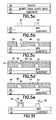
- FIG. 1is a TEM micrograph of a prior art FET with six fins
- FIGS. 2 a and 2 bare prior art diagrams showing how the lattice structure of silicon is strained when disposed adjacent to germanium ( FIG. 2 b ) as opposed to its natural state ( FIG. 2 a );
- FIG. 3is a block diagram depicting a FinFET in which the present invention may be disposed
- FIG. 4is a sectional view of FIG. 3 along section lines 4 ′— 4 ′;
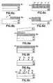
- FIGS. 5 a - 5 fare enlarged cross sectional views depicting one method of making a channel according to the present invention, using masking and etching to deposit a channel envelope onto a channel core;
- FIGS. 6 a - 6 hare enlarged cross sectional views depicting an alternative method of making at least one channel using a carrier wafer and a handle wafer;
- FIGS. 7 a - 7 fare enlarged cross sectional views depicting an alternative method of making a channel for a PFET using a shallow trench;
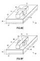
- FIGS. 8 a - 8 fare perspective views of various embodiments of FinFET devices.
- FIG. 9depicts a SRAM circuit and is useful when discussing quantization.
- FIGS. 1 and 2 a 14 2 bare described above and serve as context for understanding the present invention.
- FIG. 3depicts in block diagram a FET 10 .
- a source 12 and drain 14are connected electrically via a channel 16 , which is crossed by a gate 18 .
- One or more channels 16 and gates 18may be present in a single FET 10 .
- the length of the channel 16is the distance from the source 12 to the drain 14 as depicted in FIG. 3 .
- a sectional view of the channel 16 at section line 4 ′— 4 ′is depicted at FIG. 4 .
- the FET 10is disposed on a substrate 20 such as silicon 21 overlain with a layer of buried oxide 22 .
- a channel core 24is made from a first semiconductor material disposed over the substrate 20 .
- the substrate 20is preferably silicon based, such as a SIMOX wafer, a bonded wafer, or CZ silicon (silicon wafer from the Czochralski process) as known in the art.
- the channel core 24is formed atop the buried oxide layer 22 that forms part of the substrate 20 .
- the channel core 24defines a bottom surface 27 (shown as attached to the substrate 20 ), a top surface 26 spaced from the substrate 20 and opposed sidewalls 28 , 30 disposed between the substrate 20 and the top surface 26 .
- the first semiconductor material from which the channel core 24 is madedefines a first natural crystalline lattice structure.
- a natural lattice structure for a particular materialrefers to the lattice structure of the particular material in question in its natural state, that is, without having been stretched, compressed, or otherwise strained by external manipulation such as was previously described for strained silicon.
- a compound exhibiting a relaxed lattice structure, wherein the relaxation is due only to annealing or other processing that purposefully removes tensile or compressive forces that would otherwise be present,is not considered herein to be the natural state lattice structure.
- a channel envelope 32is disposed to substantially cover that portion of the channel core 24 that is not in direct contact with the substrate 20 when the channel 16 is viewed in cross section, at least at the portion of the channel 16 crossed by the gate 18 .
- the channel envelope 32is coupled to the top surface 26 and both opposed sidewalls 28 , 30 of the channel core 24 .
- the channel envelope 32is formed from a second semiconductor material that defines a second natural crystalline lattice structure that differs from the first lattice structure. The different natural lattice structures of the first and second semiconductor materials cause either tensile or compressive stresses at least at the boundary of the channel core 24 and the channel envelope 32 .
- the channel core 24defines a core width w c and a core height h c .
- the channel envelope 32defines an envelope width w e and an envelope height h e . Any, or all, of these dimensions may be selected to optimize or otherwise control the combined surface area of the opposed sidewalls 28 , 30 and the top surface 26 .
- Threshold voltage of a FET 10 using the inventive channel 16 described hereincan be selected based on the particular materials of either or both of the first and second semiconductor materials, the presence of a dopant in one or the other, or the core 24 and envelope 32 dimensions.
- the first semiconductor material that comprises the channel core 24is silicon
- the second semiconductor material that comprises the channel envelope 32is a compound comprising silicon and germanium, such as Si 0.7 Ge 0.3 .
- the first semiconductor material that comprises the channel core 24is preferably a compound comprising silicon and germanium that is processed to exhibit a relaxed lattice structure
- the second semiconductor material that comprises the channel envelope 32is preferably silicon.
- the gate 18which may be formed of poly or metal or other material as known in the art, is disposed over the channel 16 so as to contact the channel envelope 32 through a dielectric layer 33 , also termed a gate dielectric, disposed about the channel envelope 32 .
- the dielectric layer 33may include an oxide, oxynitride, or rare earth oxide (e.g., hafnium oxide).
- the channel envelope 32is disposed so as to prevent substantial, and preferably complete, contact between the gate 18 and the channel core 24 .
- FIG. 5illustrates a preferred method for making a FET 10 in accordance with the teachings herein.
- FIGS. 5 a-fdepict one embodiment, wherein both a PFET channel 34 and a NFET channel 36 are disposed on a single substrate 20 .
- a substrate 20 including a buried oxide layer (BOX) 22is provided and overlain with a layer of a first semiconductor material 38 , such as silicon.
- the combination of substrate layer 20 , BOX layer 22 , and layer of first semiconductor material 38may be provided by a SIMOX wafer, may be a bonded wafer, or may be provided by a Czochralski process as known in the art.
- a first channel core 40 and a second channel core 42are defined from the layer of first semiconductor material 38 by masking and etching, or by other means known in the art. The length and/or width of the first channel core 40 may differ from that of the second channel core 42 .
- 5 cdepicts a mask 44 (two masks shown) over the second channel core 42 and over all areas except the immediate vicinity of the first channel core 40 .
- Etching or other known processesmay be used to remove the mask 44 from contact with opposed sidewall surfaces of the first channel core 40 , or to prevent the mask 44 from ever contacting such sidewalls.
- the first channel core 40will become the PFET channel 34 .
- FIG. 5 ddepicts deposition of a layer of second semiconductor material 46 over the entire wafer.
- the layer of second semiconductor material 46is a compound of Si and Ge that is deposited via ultra-high vacuum chemical vapor deposition (UHVCVD), but other chemical deposition processes are also compatible.
- the layer 46defines a thickness in the range of 5-10 nm, and the thickness of the layer 46 is determined by the concentration of germanium and criterion related to layer thermal stability for such germanium concentration.
- the entity of FIG. 5 dis planarized in FIG. 5 e to remove that portion of the entire layer of second semiconductor material 46 that overlies the mask 44 . The remainder of the mask 44 is removed in FIG.
- SiGe layer 46can be selectively deposited on an exposed silicon channel core 40 and any residual removed via a chemical etch.
- the layer of first semiconductor material 38is silicon and the layer of second semiconductor material 46 is Si x Ge 1-x
- the channel envelope 32 formed by the Si x Ge 1-x compoundis under compressive stress due to the smaller natural lattice structure of the underlying Si layer 38 .
- FIG. 6An alternative method is depicted in FIG. 6 .
- a handle wafer 48includes a buried oxide layer 22 as previously described, and an overlying layer of first semiconductor material 38 , such as silicon.
- FIG. 6 bdepicts use of masking and etching to define to define one or more trenches 47 adjacent to a remaining portion 38 a of the layer of first semiconductor material 38 .
- the trenches 47 and/or the remaining portions 38 a of the layer of first semiconductor material 38may or may not be contiguous. Parallel to, or at a separate time from, the processing depicted in FIGS.
- a separate carrier wafer 50is overlain with a layer of second semiconductor material 46 , such as strained or relaxed SiGe, in FIG. 6 c .
- the carrier wafer 50 with overlayer 46is then subjected to ion implantation at FIG. 6 c .
- implantation with ions 52such as hydrogen or boron ions allows the overlayer 46 to be annealed and separated from the carrier wafer 50 at a temperature generally less than about 600° C., while also providing high quality SiGe free from dislocations. Nearly complete ( ⁇ 95%) strain relaxation of the SiGe layer 46 can also be achieved.
- a thin oxide layer 51is disposed over at least the islands 49 to facilitate later bonding to the handle wafer 48 .
- further processingmay be according to known finfet processing techniques, such as, for example, sidewall image transfer.
- FIG. 6 edepicts the structure of FIG. 6 d brought together with the structure of FIG. 6 b .
- the carrier wafer 50is inverted over the handle wafer 48 .
- the islands 49 and trenches 47are precision aligned with one another, preferably accurate to within 0.25 microns.
- the anneal process described above for the smart-cut techniqueis employed to remove the islands 49 from the carrier wafer 50 .
- the islands 49then lie within the trenches 47 , and are bonded to the handle wafer 48 by the thin oxide layer 51 .
- the carrier wafer 50is removed, preferably for later reuse as a handle wafer after a high temperature anneal and polishing.
- vertical etches through the overlayer 46 and selective ion implantation bounded by those vertical etchesis used to combine more than one layer (more than one type of semiconductor material) into an island 49 .
- Such an island 49may be disposed to match a recessed trench 47 on the handle wafer 48 as previously described, or it may be deposited on an elevated surface of silicon or other semiconductor material on the handle wafer 48 .
- FIG. 6 fshows smoothing of the exposed surfaces of the islands 49 and of the remaining portions 38 a , where these surfaces are opposite the handle wafer 48 . Smoothing and polishing is used to achieve a substantially uniform height.
- FIG. 6 gdepicts a step wherein both the island 49 and the remainder 38 a are masked and etched, or otherwise processed, to define one or more PFET channel cores 53 and preferably also one or more NFET channel cores 55 . While it is preferable to fabricate the PFET and NFET channels simultaneously as described herein, the present invention does not so require.
- an epitaxial layer of a semiconductor material different from the first semiconductor materialis grown or disposed on the PFET channel cores 53 to form channel envelopes 32 , creating a strained silicon or other hetero-layer.
- the material of the channel envelope 32may be strained or unstrained, depending upon the desired properties of the resultant channel 16 .
- Maximum lattice discontinuityoccurs along the lines defined by either of the opposed sidewall surfaces 28 , 30 and the bottom surface 27 /top surface 26 of the channel core 24 .
- the PFET channel 34 or NFET channel 36are characterized by a width of about 100-150 ⁇ and a height of about 500-600 ⁇ . These dimensions may change with scaling.
- the strained latticeis disposed along both the sidewalls 28 , 30 and the top 26 of the PFET channel 34 or NFET channel 36 .
- SRAMstatic random access memory
- DRAMdynamic RAM
- SRAMis a type of memory that does not need to be refreshed like dynamic RAM (DRAM), so SRAM is generally much faster (typically about 10 ns for SRAM versus about 60 ns for DRAM) and more reliable.
- the cycle time (a measurement of how quickly two back-to-back accesses of a memory chip can be made) of SRAMis much shorter than that of DRAM because it does not need to pause between accesses.
- the design of SRAMsgenerally assumes FETs in several fixed sizes (quantized).
- the width of the channel 16is critical for stability in SRAM, and thereby imposes a tradeoff between size and stability.
- a FET 10 employing a fin according to the present inventionmay be used to modulate the height of the channel to enable a smaller FET 10 that still ensures SRAM stability.
- the starting siliconwould be at least as high as the highest estimated fin.
- Selective masking and etching of certain devices within a celltailors fin height to achieve the desired SRAM stability.
- a slow etchis used to ensure uniformity and fine control over fin height.
- effective channel widthcan be adjusted by using multiple fins, preferably in a side-by-side relation.
- FIG. 7is a series of block diagrams showing process steps in forming a PFET.
- FIG. 7depicts a shallow trench isolation (STI) that is imposed between a first semiconductor material, such as SiGe, and a second semiconductor material, such as Si.
- a substrate 20supports a buried oxide layer (BOX) 22 , which is overlain with a layer of a first semiconductor material 38 , such as silicon.
- the substrate/BOX/overlayer combination 70may be a SIMOX wafer, a bonded wafer, or a CZ wafer as previously described and known in the art.
- a trench 58is formed and filled with an oxide or other insulator such as TEOS, as is known in the art. It is noted that the trenching and filling represented by FIG. 7 b is performed in several steps, and the trench 58 divides the layer of first semiconductor material 38 into a first region 62 and a PFET region 64 . Alternatively, the trench 58 may be etched, but not filled, without departing from the advantages of the present invention.
- a mask layer 44is selectively disposed over the trench 58 and the first region 62 of the first semiconductor material. In FIG.
- the PFET region 64is then etched back to a thin layer 60 , preferably to a thickness on the order of 10 nm.
- a layer of second semiconductor material 46is disposed over the thin layer 60 .
- the thin layer 60includes a horizontal surface 67 , and a substantially vertical surface 68 .
- the second semiconductor material 46is SiGe of a moderate concentration.
- 10%-20% Ge concentrationis preferable when the thickness of the layer 46 is between about 10-30 nm. It has been found that thicker layers 46 of SiGe, and/or higher concentrations of Ge, will be metastable and may require further thermal processing, though not annealing.
- Any embodiment of the present inventionpreferably includes an enveloping layer of gate dielectric or gate oxide.
- a channel 16 according to the present inventionmay be part of a FinFET 10 , as in FIG. 3 , and the FinFET 10 may preferably be part of an integrated circuit 100 .
- the channel 16may include a channel core 24 that has substantially upstanding sidewalls 28 , 30 , a top surface 26 , and a bottom surface 27 , as in FIG. 4 , or may be fabricated to define only a horizontal surface 67 and substantially vertical surfaces 68 as in FIG. 7 e .
- the channel 16may have two sidewall surfaces 74 that extend from the substrate 22 and join at an acute or rounded peak 71 so as to define a substantially triangular cross section 75 , as opposed to the rectangular cross sections illustrated herein, such as the cross section of the thin layer 60 .
- a channel defining a non-orthogonal cross sectionwould be optimized using strained silicon on the top and in contact with the gate oxide.
- the channel envelope 32may contact any two of the surfaces 26 , 27 , 28 , 30 of the channel core 24 , or all such surfaces 26 , 28 , 30 not contacting the substrate 20 .
- a broader surface of the strained lattice structures that carry charge (electrons or holes)is better exposed to the gate 18 as compared to prior art FinFETs, enabling greater control by the gate 18 and more efficient current transport.
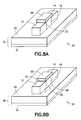
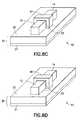
- FIG. 8represents various additional embodiments of FinFET structures in accordance with the teachings herein.
- the structuresinclude a relaxed Si—Ge layer with an overlying strained Si layer. This combination provides for improved electron-hole mobility.
- the channel 16 shown in FIGS. 8A-Bis formed of a channel core 24 and is overlain with the channel envelope 32 , as is shown in FIG. 4 .
- the substrate 20includes the buried oxide layer 22 , and the Si layer 21 .
- Each structure depicted in FIG. 8includes the source 12 , a drain 14 , the gate 18 , and the channel 16 .
- a dielectric layer 33disposed between the channel 16 and the various gates.
- the channel 16is internal to the structures shown in FIGS. 8C-E , and is therefore not visible, the channel 16 is only depicted in FIGS. 8A-B and 8 F. Regardless, each of the embodiments of FIGS. 8A-8F may include the channel core 24 and channel envelope 32 as previously described.
- FIG. 8Aa single gate FinFET 90 is shown.
- the channel 16includes a relaxed Si-Ge layer, and a strained Si layer.
- a thin oxide layer 33is disposed between the channel 16 and a single gate 95 .
- FIG. 8Brepresents a double gate 91 embodiment of a FinFET.
- a second gate 96is presented.
- the second gate 96is buried within a trench in the buried oxide layer 22 .
- FIG. 8Crepresents a triple gate FinFET 92 , wherein a triple gate 97 is formed over the thin oxide layer 33 , which is disposed over the channel 16 (shown in FIGS. 8 A-B).
- FIG. 8Drepresents a quadruple gate FinFET 93 , wherein a quadruple gate 98 effectively surrounds the channel 16 .
- FIG. 8Da portion of the quadruple gate 98 is submerged in the buried oxide layer 22 .
- FIG. 8Ea FinFET 94 having a Pi gate 99 is shown. The Pi gate 99 extends downward, and at least partially into the buried oxide layer 22 .
- FIG. 8Fis another embodiment of a double gate FinFET 87 , defining a first gate 88 and a second gate 89 .
- the FinFET of FIG. 8Fmay be formed, for example, by polishing the FinFET of FIG. 8C until the portion of the triple gate 97 of FIG. 8C that overlies the channel 16 is removed, leaving the two gates 88 , 89 of FIG. 8 F.
- the channelincludes strained silicon germanium.
- each gate 88 , 89may be independently controlled so that, for example, the first gate 88 is a typical FinFET gate and the second gate 89 may apply variable voltage.
- the second gate 89is a back gate to control a depletion region, when current between the source 12 and drain 14 is switched between on and off.
- Such a second gate 89better controls leakages and performance of the first gate 88 by use of the variable voltage; so that only the minimum voltage necessary to control leakage current is applied.
- the [110] directionis at a 45° angle to the crystalline axes.
- FIG. 9depicts one embodiment of a six transistor SRAM unit cell.
- PFET quantizationis carried out on the smallest device in a six-transistor conventional SRAM (e.g., NFET pass gate 77 (Pg) and pull-up PFET 76 (PL) is smaller in size).
- NFET pass gate 77Pg
- PLpull-up PFET 76
- fin height quantizationcan be based on individual devices, or bucketing pass gate NFET and pull up PFET into one quanta height and larger NFET 78 (Cc) into another.
- a smaller fin heightwhich is employed in multiples of NFET and PFET devices of the embodiment shown in FIGS. 8A-F , may be used. This quantization will help to make a robust and stable cell.
Landscapes
- Insulated Gate Type Field-Effect Transistor (AREA)
- Thin Film Transistor (AREA)
- Metal-Oxide And Bipolar Metal-Oxide Semiconductor Integrated Circuits (AREA)
Abstract
Description
These teachings relate generally to field effect transistors (FET) disposed on a semiconductor wafer or chip, in particular, to a layered structure as a channel that connects a source and a drain of a FET, wherein one of the layers is characterized by a strained lattice structure.
Semiconductors and integrated circuit chips have become ubiquitous within many products due to their continually decreasing cost and size. Miniaturization in general allows increased performance (more processing per clock cycle and less heat generated) at lower power levels and lower cost. Present technology is at or approaching atomic-level scaling of certain micro-devices such as logic gates, FETs, capacitors, etc. Circuit chips with hundreds of millions of such devices are not uncommon. Further size reductions appear to be approaching the physical limit of trace lines and micro-devices that are embedded upon and within their semiconductor substrates. The present invention is directed to such micro-sized FET devices. A FET is a transistor consisting of a source, a gate, and a drain. The action of the FET depends on the flow of majority carriers along a channel between the source and drain that runs past the gate. Current through the channel, which is between the source and drain, is controlled by the transverse electric field under the gate. More than one gate may be used to more effectively control the channel. The length of the gate determines how fast the FET switches and how fast the circuit can operate, and is generally about the same as the length of the channel (i.e., the distance between the source and drain). State of the art gate lengths are today on the order of 50 nm, and are moving toward 10 nm within the next decade. Such size reductions should enable upwards of a billion devices on a single chip. However, such small scaling necessitates greater control over performance issues such as short channel effects, punch-through, and MOS leakage current.
Recently, the size of FETs has been successfully reduced through the use of one or more fin-shaped channels, known as fins. FETs employing fins are known as FinFETs. Previously, complementary metal-oxide semiconductor (CMOS) devices were substantially planar along the surface of the semiconductor substrate, the exception being the FET gate that was disposed over the top of the channel. Fins break from that paradigm by using a vertical structure in order to maximize surface area of the channel that is exposed to the gate. The gate controls the channel more strongly because it extends over three sides of the fin shaped channel, rather than only across the top of a more traditional planar channel. An example of a FinFET is shown inFIG. 1 , which is a TEM micrograph of a prior art FET with six fins. Each pair of fins comprises an NFET and a PFET.
One method to enhance fin performance is to fabricate fins in layers of disparate materials. One such exemplary device assigned to the assignee of this invention is described in U.S. Pat. No. 6,252,284 B1, “Planarized Silicon Fin Device”, which is directed to controlling short-channel effects.
Often, one of the layers of a multi-layered planarized FET fin is strained silicon. It has been previously discovered that biaxially stretching the crystalline lattice structure of silicon can speed the flow of electrons through a transistor, thereby enhancing performance and decreasing power consumption. There is a natural tendency of atoms in layers of disparate materials to align with one another by stretching and/or compressing their mismatched lattice structures along a planar interface of the mismatch. Varying the respective thickness and chemical composition of the materials aids in controlling the extent of extension and compression in either material. As an example,FIG. 2 adepicts a silicon lattice structure and a germanium lattice structure, not to scale, in their natural (unstretched) states. When silicon is disposed (or grown) on a thicker layer of germanium, as in the SiGe compound ofFIG. 2 b, the lattice of silicon stretches while the lattice of germanium remains substantially unchanged, resulting in strained silicon.
This result is achieved as the comparatively greater thickness of the germanium layer yields greater structural integrity and greater resistance to lattice compression. The actual process of lattice stretching may also, or alternatively, entail atoms of Si and Ge intermixed within a lattice structure. This integrates both atoms within a single layer, wherein the larger Ge atoms force the integrated lattice structure to stretch, as compared to a natural (unstretched) silicon lattice structure. The opposite effect from that shown inFIG. 2 bcan also be realized, wherein a thinner layer of germanium exhibits lattice compression when bonded to a thicker layer of silicon. Strained silicon has been shown to enhance electron/hole mobility by up to 70% in NFETs, and up to 30% in PFETs. Other materials such as silicon germanium carbon may be used to form the crystalline heterojunction that enhances conductivity. There are several methods used to form strained layers, including chemical vapor deposition (CVD) and molecular beam epitaxy (MBE).
Strained silicon disposed along a plane has been used in prior art FinFETs. However, current leakage continues to be a limiting factor in further scaling of FETs toward the atomic limit. Current leakage becomes an ascendant concern as miniaturization progresses because shorter length FET gates, which generally track the channel length, have less ability to control electric charge carriers (holes or electrons).
The unintentional flow of charge carriers when the transistor is off is termed “current leakage.” Current leakage is the primary source of power consumed by an idle transistor. Current leakage may be classified into two types: MOS off current, wherein an unintended current passes through the channel despite the gate attempting to shut off current completely; and gate tunneling leakage current, wherein unintended current follows a parasitic pathway flowing into the channel, diffusions, or silicon body. As FET channel lengths continue to decrease, it is expected that gate tunneling leakage current will become a predominant concern for designers. The fin structure enhances gate control over the channel, but gate control over current is not absolute, even in prior art FinFETs. Compounding the current leakage problem, miniaturization enables ever-lower power levels that require more absolute gate control. Current leakage that escapes the gate's control is less distinguishable from intentional current, particularly at low current levels.
What is needed is a FET that allows small scaling with enhanced performance for both NFETs and PFETs. Preferably, the FET should improve gate control in a fin structure that exhibits enhanced carrier transport properties.
The foregoing and other problems are overcome, and other advantages are realized, in accordance with the presently preferred embodiments of these teachings. The present invention concerns a channel for electrically connecting a source and a drain of a field effect transistor (FET), commonly called a fin for a FinFET. The channel includes a channel core and a channel envelope. The channel core is coupled to a substrate such as a SIMOX wafer (a wafer with an upper region separated by implanted oxygen) or bonded wafer. The channel core defines a top surface that is spaced from the substrate, and opposed sidewall surfaces between the substrate and the top surface. The channel core is formed from a first semiconductor material defining a first lattice structure.
The channel envelope is in contact with the opposed sidewall surfaces and the top surface of the channel core. The channel envelope is formed from a second semiconductor material defining a second lattice structure that differs from the first lattice structure. This difference in lattice structure provides enhanced electrical conductivity due to stretching or compressing of the lattice structure. Preferably, the two materials are silicon and a silicon-germanium compound.
In another aspect of the present invention, the channel core defines a top and an adjoining side surface. In a preferred embodiment, the top surface is the horizontal top and the side surface is one of two upstanding sidewalls of the channel core, although two upstanding surfaces extending from the substrate and meeting at a peak, or two sidewalls joined by a third lateral surface may be used. The channel core comprises a first semiconductor material and the channel envelope comprises a second semiconductor material that differs from the first. At least one of the first or second semiconductor materials exhibits enhanced electrical conductivity due to one of a stretched or compressed lattice structure. The channel envelope is in contact with both the top and side surfaces, providing a larger area of interface between the disparate lattice materials, as compared to prior art channels that provide interface only along a top surface. The exemplary materials noted above are operable to provide the stretched or compressed lattice structure.
The present invention also includes methods of making a FET channel. In one such method, a substrate is provided with an overlying layer of a first semiconductor material. A first channel core is defined from the overlying layer, such as by a mask and etch technique. The channel core defines a top surface spaced from the substrate and opposed first and second sidewalls between the substrate and the top surface. The method further includes disposing a layer of second semiconductor material to contact at least two of the surfaces (that is, at least two of the top surface, the first sidewall and the second sidewall). Electrical conductivity through the layer of second semiconductor material, which is different from the first, is enhanced by its contact with the channel core. The layer of second semiconductor material may be deposited via vacuum deposition, or may be grown on a carrier wafer and separated therefrom to contact the appropriate surfaces of the channel core.
Another method of forming the channel includes providing a first layer of a semiconductor material over a substrate. This method includes defining a trench in the overlayer, and the overlayer is then divided into a first section and a second section by the trench. The trench may be filled with a buffer material such as TEOS (also known as tetraethoxysilane, tetraethylorthosilicate, tetraethelorthosilicate, and tetrethoxysilicide). A portion of the second section is then removed to leave a remaining layer of first semiconductor material that has a thickness less than a depth of the trench. This exposes a portion of the trench. The method then includes disposing a layer of a second semiconductor material over the remaining layer and adjacent to the trench. Exemplary semiconductor materials are discussed above. Preferably, the remaining layer is less than about 15 nm. Where the second semiconductor material is SixGe1-x, the relative concentration of germanium may be chosen to promote thermal stability of the channel. Preferably, the germanium content is between about 8% and about 22%, and most preferably between about 10% and about 20%, and a low temperature chemical vapor deposition process is used to form the layer of second semi-conductor material.
Further, disclosed herein is a channel for electrically connecting a source and a drain of a field effect transistor (FET) comprising: a channel core comprising a bottom surface coupled to a substrate and defining a top surface spaced from the substrate and opposed sidewall surfaces between the bottom surface and the top surface, wherein the channel core is formed from a first semiconductor material defining a first lattice structure; and a channel envelope in contact with at least one of the top surface, the bottom surface and one of the sidewall surfaces (or combinations thereof), wherein the channel envelope comprises a second semiconductor material comprising a strained lattice structure that differs from the first lattice structure, the channel envelope being electrically coupled to a gate electrode. Preferably, the channel is formed of a relaxed Si—Ge lattice, and the envelope is formed of a strained Si lattice.
An exemplary circuit SRAM circuit using FinFET in accordance with the teachings herein is disclosed.
The foregoing and other aspects of these teachings are made more evident in the following Detailed Description of the Preferred Embodiments, when read in conjunction with the attached Drawing Figures, wherein:
A sectional view of thechannel 16 atsection line 4′—4′ is depicted at FIG.4. The FET10 is disposed on asubstrate 20 such assilicon 21 overlain with a layer of buriedoxide 22. Achannel core 24 is made from a first semiconductor material disposed over thesubstrate 20. Thesubstrate 20 is preferably silicon based, such as a SIMOX wafer, a bonded wafer, or CZ silicon (silicon wafer from the Czochralski process) as known in the art. Preferably, thechannel core 24 is formed atop the buriedoxide layer 22 that forms part of thesubstrate 20. Thechannel core 24 defines a bottom surface27 (shown as attached to the substrate20), atop surface 26 spaced from thesubstrate 20 andopposed sidewalls substrate 20 and thetop surface 26. The first semiconductor material from which thechannel core 24 is made defines a first natural crystalline lattice structure. As used herein, unless specifically noted otherwise, a natural lattice structure for a particular material (element or compound) refers to the lattice structure of the particular material in question in its natural state, that is, without having been stretched, compressed, or otherwise strained by external manipulation such as was previously described for strained silicon. A compound exhibiting a relaxed lattice structure, wherein the relaxation is due only to annealing or other processing that purposefully removes tensile or compressive forces that would otherwise be present, is not considered herein to be the natural state lattice structure.
Achannel envelope 32 is disposed to substantially cover that portion of thechannel core 24 that is not in direct contact with thesubstrate 20 when thechannel 16 is viewed in cross section, at least at the portion of thechannel 16 crossed by thegate 18. Preferably, thechannel envelope 32 is coupled to thetop surface 26 and both opposed sidewalls28,30 of thechannel core 24. Thechannel envelope 32 is formed from a second semiconductor material that defines a second natural crystalline lattice structure that differs from the first lattice structure. The different natural lattice structures of the first and second semiconductor materials cause either tensile or compressive stresses at least at the boundary of thechannel core 24 and thechannel envelope 32. This mismatch of natural lattices, herein termed a “heterojunction,” facilitates carrier transport where the gate dielectric contacts the heterojunction stack. However, carrier transport is not necessarily maximized at the heterojunction; the main channel for carrier transport may alternately form within one or the other disparate materials, as known in the art, depending upon several factors. Thechannel core 24 defines a core width wcand a core height hc. Similarly, thechannel envelope 32 defines an envelope width weand an envelope height he. Any, or all, of these dimensions may be selected to optimize or otherwise control the combined surface area of the opposedsidewalls top surface 26. Where thechannel core 24 and/orenvelope 32 are not rectangular shaped (as primarily illustrated herein), such as when thechannel core 24 is triangular and thechannel envelope 32 is disposed over two sides of thechannel core 24, the width and height are deemed to be averages for the particular component. Threshold voltage of a FET10 using theinventive channel 16 described herein can be selected based on the particular materials of either or both of the first and second semiconductor materials, the presence of a dopant in one or the other, or thecore 24 andenvelope 32 dimensions.
Preferably for a PFET, the first semiconductor material that comprises thechannel core 24 is silicon, and the second semiconductor material that comprises thechannel envelope 32 is a compound comprising silicon and germanium, such as Si0.7Ge0.3. For a NFET, the first semiconductor material that comprises thechannel core 24 is preferably a compound comprising silicon and germanium that is processed to exhibit a relaxed lattice structure, and the second semiconductor material that comprises thechannel envelope 32 is preferably silicon.
Thegate 18, which may be formed of poly or metal or other material as known in the art, is disposed over thechannel 16 so as to contact thechannel envelope 32 through adielectric layer 33, also termed a gate dielectric, disposed about thechannel envelope 32. Thedielectric layer 33 may include an oxide, oxynitride, or rare earth oxide (e.g., hafnium oxide). Thechannel envelope 32 is disposed so as to prevent substantial, and preferably complete, contact between thegate 18 and thechannel core 24.
InFIG. 5 a, asubstrate 20 including a buried oxide layer (BOX)22 is provided and overlain with a layer of afirst semiconductor material 38, such as silicon. The combination ofsubstrate layer 20,BOX layer 22, and layer offirst semiconductor material 38 may be provided by a SIMOX wafer, may be a bonded wafer, or may be provided by a Czochralski process as known in the art. InFIG. 5 b, afirst channel core 40 and asecond channel core 42 are defined from the layer offirst semiconductor material 38 by masking and etching, or by other means known in the art. The length and/or width of thefirst channel core 40 may differ from that of thesecond channel core 42.FIG. 5 cdepicts a mask44 (two masks shown) over thesecond channel core 42 and over all areas except the immediate vicinity of thefirst channel core 40. Etching or other known processes may be used to remove themask 44 from contact with opposed sidewall surfaces of thefirst channel core 40, or to prevent themask 44 from ever contacting such sidewalls. Thefirst channel core 40 will become thePFET channel 34.
An alternative method is depicted in FIG.6. InFIG. 6 a, ahandle wafer 48 includes a buriedoxide layer 22 as previously described, and an overlying layer offirst semiconductor material 38, such as silicon.FIG. 6 bdepicts use of masking and etching to define to define one ormore trenches 47 adjacent to a remainingportion 38aof the layer offirst semiconductor material 38. Considering the entire expanse of thehandle wafer 48, thetrenches 47 and/or the remainingportions 38aof the layer offirst semiconductor material 38 may or may not be contiguous. Parallel to, or at a separate time from, the processing depicted inFIGS. 6 a-6b, aseparate carrier wafer 50 is overlain with a layer ofsecond semiconductor material 46, such as strained or relaxed SiGe, inFIG. 6 c. Thecarrier wafer 50 withoverlayer 46 is then subjected to ion implantation atFIG. 6 c. As known in the art, implantation with ions52 such as hydrogen or boron ions allows theoverlayer 46 to be annealed and separated from thecarrier wafer 50 at a temperature generally less than about 600° C., while also providing high quality SiGe free from dislocations. Nearly complete (≧95%) strain relaxation of theSiGe layer 46 can also be achieved. The above process is generally known in the art as a “smart-cut” technique, and is more particularly described by Lijuan Huang et al, ELECTRON AND HOLE MOBILITY ENHANCEMENT IN STRAINED SOIBY WAFER BONDING , IEEE Transactions on Electron Devices., vol. 49, no. 9, September 2002, pp 1566-1571, herein incorporated by reference. AtFIG. 6 d, masking and etching are used to define one ormore islands 49 from the second layer ofsemiconductor material 46. The shapes of theislands 49 on thecarrier wafer 50 are complementary to the shapes of thetrenches 47 on thehandle wafer 48. Preferably, athin oxide layer 51 is disposed over at least theislands 49 to facilitate later bonding to thehandle wafer 48. Once theislands 49 are formed, further processing may be according to known finfet processing techniques, such as, for example, sidewall image transfer.
The material of thechannel envelope 32 may be strained or unstrained, depending upon the desired properties of theresultant channel 16. Maximum lattice discontinuity occurs along the lines defined by either of the opposed sidewall surfaces28,30 and thebottom surface 27/top surface 26 of thechannel core 24.
Preferably, thePFET channel 34 orNFET channel 36 are characterized by a width of about 100-150 Å and a height of about 500-600 Å. These dimensions may change with scaling. Preferably, the strained lattice is disposed along both thesidewalls PFET channel 34 orNFET channel 36.
One particular application in which the carrier pathway along the strained sidewall can be exploited is in a FET10 in a static random access memory (SRAM). SRAM is a type of memory that does not need to be refreshed like dynamic RAM (DRAM), so SRAM is generally much faster (typically about 10 ns for SRAM versus about 60 ns for DRAM) and more reliable. In addition, the cycle time (a measurement of how quickly two back-to-back accesses of a memory chip can be made) of SRAM is much shorter than that of DRAM because it does not need to pause between accesses. The design of SRAMs generally assumes FETs in several fixed sizes (quantized). However, the width of thechannel 16 is critical for stability in SRAM, and thereby imposes a tradeoff between size and stability. Rather than select a FET with a quantized channel width that may be larger in the x-y plane (the plane ofFIG. 3 ) than desirable, a FET10 employing a fin according to the present invention may be used to modulate the height of the channel to enable a smaller FET10 that still ensures SRAM stability. During fabrication, the starting silicon would be at least as high as the highest estimated fin. Selective masking and etching of certain devices within a cell tailors fin height to achieve the desired SRAM stability. Preferably, a slow etch is used to ensure uniformity and fine control over fin height. Additionally, effective channel width can be adjusted by using multiple fins, preferably in a side-by-side relation.
Preferably, thesecond semiconductor material 46 is SiGe of a moderate concentration. For thermally stable fins, 10%-20% Ge concentration is preferable when the thickness of thelayer 46 is between about 10-30 nm. It has been found thatthicker layers 46 of SiGe, and/or higher concentrations of Ge, will be metastable and may require further thermal processing, though not annealing. Any embodiment of the present invention preferably includes an enveloping layer of gate dielectric or gate oxide. Achannel 16 according to the present invention may be part of a FinFET10, as inFIG. 3 , and the FinFET10 may preferably be part of an integrated circuit100. Thechannel 16 may include achannel core 24 that has substantiallyupstanding sidewalls top surface 26, and abottom surface 27, as inFIG. 4 , or may be fabricated to define only ahorizontal surface 67 and substantiallyvertical surfaces 68 as inFIG. 7 e. As a further alternative, shown inFIG. 7 f, thechannel 16 may have twosidewall surfaces 74 that extend from thesubstrate 22 and join at an acute or roundedpeak 71 so as to define a substantially triangular cross section75, as opposed to the rectangular cross sections illustrated herein, such as the cross section of thethin layer 60. It is anticipated that a channel defining a non-orthogonal cross section would be optimized using strained silicon on the top and in contact with the gate oxide. Thechannel envelope 32 may contact any two of thesurfaces channel core 24, or allsuch surfaces substrate 20. In any embodiment above, a broader surface of the strained lattice structures that carry charge (electrons or holes) is better exposed to thegate 18 as compared to prior art FinFETs, enabling greater control by thegate 18 and more efficient current transport.
Thechannel 16 shown inFIGS. 8A-B , is formed of achannel core 24 and is overlain with thechannel envelope 32, as is shown in FIG.4. As shown inFIG. 8 , thesubstrate 20 includes the buriedoxide layer 22, and theSi layer 21. Each structure depicted inFIG. 8 includes thesource 12, adrain 14, thegate 18, and thechannel 16. Also shown is adielectric layer 33 disposed between thechannel 16 and the various gates. As thechannel 16 is internal to the structures shown inFIGS. 8C-E , and is therefore not visible, thechannel 16 is only depicted inFIGS. 8A-B and8F. Regardless, each of the embodiments ofFIGS. 8A-8F may include thechannel core 24 andchannel envelope 32 as previously described.
InFIG. 8A , asingle gate FinFET 90 is shown. In this embodiment, thechannel 16 includes a relaxed Si-Ge layer, and a strained Si layer. Athin oxide layer 33 is disposed between thechannel 16 and asingle gate 95.FIG. 8B represents adouble gate 91 embodiment of a FinFET. In addition to thesingle gate 95 shown inFIG. 8A , asecond gate 96 is presented. In this embodiment, thesecond gate 96, is buried within a trench in the buriedoxide layer 22.FIG. 8C represents atriple gate FinFET 92, wherein atriple gate 97 is formed over thethin oxide layer 33, which is disposed over the channel16 (shown in FIGS.8A-B).FIG. 8D represents aquadruple gate FinFET 93, wherein aquadruple gate 98 effectively surrounds thechannel 16. InFIG. 8D , a portion of thequadruple gate 98 is submerged in the buriedoxide layer 22. InFIG. 8E , aFinFET 94 having aPi gate 99 is shown. ThePi gate 99 extends downward, and at least partially into the buriedoxide layer 22.
Depositing the strained Si layer on thequadruple gate FinFET 93 and thePi gate FinFET 94, wherein theFinFET
While described in the context of presently preferred embodiments, various modifications of and alterations to the foregoing embodiments can be made with normal skill in the art, and all such modifications and alterations remain within the scope of this invention and the ensuing claims. Examples herein are considered to be illustrative and not exhaustive of the teachings of this invention.
Claims (23)
1. A channel for electrically connecting a source and a drain of a field effect transistor (FET) comprising:
a channel core coupled to a substrate and defining a top surface spaced from the substrate and opposed sidewall surfaces between the substrate and the top surface, wherein the channel core comprises a first semiconductor material defining a first lattice structure;
a channel envelope in contact with the opposed sidewall surfaces and the top surface, wherein the channel envelope comprises a second semiconductor material defining a second lattice structure that differs from the first lattice structure;
a gate oxide disposed about a surface of the channel envelope that is opposite the channel core.
2. The channel ofclaim 1 further comprising a gate coupled through the gate oxide to at least two surfaces defined by the channel envelope.
3. The channel ofclaim 1 wherein at least one of the sidewall surfaces defines a height hcand the top surface defines a width wc, and wherein hc≧3wc.
4. The channel ofclaim 1 wherein the channel is a component of an FET and the FET is a component of a SRAM, and at least one of the sidewall surfaces defines a height hcthat is selected to increase stability of the SRAM.
5. The channel ofclaim 1 wherein the top surface defines a width w that is selected to maximize one of stretching and of compressing the lattice structure of one of the first and the second semiconductor material.
6. The channel ofclaim 1 wherein the second semiconductor material substantially covers the two sidewall surfaces and the top surface.
7. The channel ofclaim 1 wherein one of the first and second semiconductor materials comprises silicon and germanium.
8. In a channel for a field effect transistor, the improvement comprising:
a channel core defining at least a top and at least one adjoining side surface;
a channel envelope in contact with the top surface and the at least one side surface;
a gate oxide disposed on at least two surfaces of the channel envelope, said surfaces of the channel envelope being opposed to the top surface and the at least one side surface;
wherein the channel core comprises a first semiconductor material and the channel envelope comprises a second semiconductor material, and at least one of the first and second semiconductor materials exhibits one of a stretched and a compressed lattice structure.
9. A field effect transistor (FET) comprising:
a channel core coupled to a substrate and defining a top surface spaced from the substrate and opposed sidewall surfaces between the substrate and the top surface, wherein the channel core comprises a first semiconductor material defining a first lattice structure;
a channel envelope in contact with the opposed sidewall surfaces and the top surface, wherein the channel envelope comprises a second semiconductor material defining a second lattice structure that differs from the first lattice structure;
a gate oxide disposed about a surface of the channel envelope that is opposite the channel core; and
a gate coupled to the channel core through the gate oxide, said gate disposed at least partially within the substrate.
10. The FET ofclaim 9 wherein the said gate is a first gate that extends parallel to one of said opposed sidewall surfaces, the FET further comprising a second gate that extends parallel to the other of said sidewall surfaces.
11. The FET ofclaim 9 wherein each of said first and second gates are disposed only partially within said substrate.
12. The FET ofclaim 11 further comprising a third gate disposed parallel to the said top surface and electrically coupling the first and second gates.
13. The FET ofclaim 12 wherein the third gate is not disposed at least partially within said substrate.
14. The FET ofclaim 9 wherein the said gate is a first gate that extends parallel to said top surface, the FET further comprising a second gate that extends parallel to said top surface and not disposed at least partially within said substrate.
15. The FET ofclaim 14 further comprising a third and fourth gate each disposed parallel to said opposed sidewalls and each electrically coupling said first and second gates to one another.
16. A field effect transistor (FET) comprising:
a channel core coupled to a substrate and defining a top surface spaced from the substrate and opposed sidewall surfaces between the substrate and the top surface, wherein the channel core comprises a first semiconductor material defining a first lattice structure;
a channel envelope in contact with the opposed sidewall surfaces and the top surface, wherein the channel envelope comprises a second semiconductor material defining a second lattice structure that differs from the first lattice structure;
a gate oxide disposed about a surface of the channel envelope that is opposite the channel core; and
first and second gates coupled to the channel core through the gate oxide, said first and second gates disposed on opposed sides of said channel core and not directly coupled to one another electrically.
17. The FET ofclaim 16 wherein said gates are disposed parallel to said top surface.
18. The FET ofclaim 17 wherein said first gate is at least partially disposed within said substrate.
19. The FET ofclaim 16 wherein said gates are disposed parallel to said opposed sidewalls.
20. The FET ofclaim 19 wherein a portion of each of said gates is disposed within said substrate.
21. The FET ofclaim 16 further comprising a first control coupled to the first gate and a second control for controlling to the second gate, wherein the first and second controls are independent of one another.
22. The FET ofclaim 21 wherein the first control comprises a first voltage source that applies a variable voltage to the first gate.
23. The FET ofclaim 22 wherein the second control operates to select between on and off for the second gate, and the first and second controls operate in conjunction with one another.
Priority Applications (10)
| Application Number | Priority Date | Filing Date | Title |
|---|---|---|---|
| US10/626,760US6921982B2 (en) | 2003-07-21 | 2003-07-21 | FET channel having a strained lattice structure along multiple surfaces |
| TW093121106ATWI281248B (en) | 2003-07-21 | 2004-07-15 | FET channel having a strained lattice structure along multiple surfaces |
| PCT/US2004/023183WO2005010944A2 (en) | 2003-07-21 | 2004-07-19 | Fet channel having a strained lattice structure along multiple surfaces |
| EP04757122AEP1652235A4 (en) | 2003-07-21 | 2004-07-19 | FET-CHANNEL WITH A STRUCTURED GRID STRUCTURE AMONG SEVERAL SURFACES |
| KR1020067000697AKR100773009B1 (en) | 2003-07-21 | 2004-07-19 | Fet channel having a strained lattice structure along multiple surfaces |
| CNB2004800210466ACN100479158C (en) | 2003-07-21 | 2004-07-19 | Fet channel having a strained lattice structure along multiple surfaces |
| US11/137,811US7198990B2 (en) | 2003-07-21 | 2005-05-24 | Method for making a FET channel |
| US11/621,290US20070111406A1 (en) | 2003-07-21 | 2007-01-09 | FET Channel Having a Strained Lattice Structure Along Multiple Surfaces |
| US11/969,992US20080105898A1 (en) | 2003-07-21 | 2008-01-07 | FET Channel Having a Strained Lattice Structure Along Multiple Surfaces |
| US11/970,011US20080105900A1 (en) | 2003-07-21 | 2008-01-07 | FET Channel Having a Strained Lattice Structure Along Multiple Surfaces |
Applications Claiming Priority (1)
| Application Number | Priority Date | Filing Date | Title |
|---|---|---|---|
| US10/626,760US6921982B2 (en) | 2003-07-21 | 2003-07-21 | FET channel having a strained lattice structure along multiple surfaces |
Related Child Applications (3)
| Application Number | Title | Priority Date | Filing Date |
|---|---|---|---|
| US11/137,811DivisionUS7198990B2 (en) | 2003-07-21 | 2005-05-24 | Method for making a FET channel |
| US11/969,992DivisionUS20080105898A1 (en) | 2003-07-21 | 2008-01-07 | FET Channel Having a Strained Lattice Structure Along Multiple Surfaces |
| US11/970,011DivisionUS20080105900A1 (en) | 2003-07-21 | 2008-01-07 | FET Channel Having a Strained Lattice Structure Along Multiple Surfaces |
Publications (2)
| Publication Number | Publication Date |
|---|---|
| US20050017377A1 US20050017377A1 (en) | 2005-01-27 |
| US6921982B2true US6921982B2 (en) | 2005-07-26 |
Family
ID=34080479
Family Applications (5)
| Application Number | Title | Priority Date | Filing Date |
|---|---|---|---|
| US10/626,760Expired - LifetimeUS6921982B2 (en) | 2003-07-21 | 2003-07-21 | FET channel having a strained lattice structure along multiple surfaces |
| US11/137,811Expired - LifetimeUS7198990B2 (en) | 2003-07-21 | 2005-05-24 | Method for making a FET channel |
| US11/621,290AbandonedUS20070111406A1 (en) | 2003-07-21 | 2007-01-09 | FET Channel Having a Strained Lattice Structure Along Multiple Surfaces |
| US11/970,011AbandonedUS20080105900A1 (en) | 2003-07-21 | 2008-01-07 | FET Channel Having a Strained Lattice Structure Along Multiple Surfaces |
| US11/969,992AbandonedUS20080105898A1 (en) | 2003-07-21 | 2008-01-07 | FET Channel Having a Strained Lattice Structure Along Multiple Surfaces |
Family Applications After (4)
| Application Number | Title | Priority Date | Filing Date |
|---|---|---|---|
| US11/137,811Expired - LifetimeUS7198990B2 (en) | 2003-07-21 | 2005-05-24 | Method for making a FET channel |
| US11/621,290AbandonedUS20070111406A1 (en) | 2003-07-21 | 2007-01-09 | FET Channel Having a Strained Lattice Structure Along Multiple Surfaces |
| US11/970,011AbandonedUS20080105900A1 (en) | 2003-07-21 | 2008-01-07 | FET Channel Having a Strained Lattice Structure Along Multiple Surfaces |
| US11/969,992AbandonedUS20080105898A1 (en) | 2003-07-21 | 2008-01-07 | FET Channel Having a Strained Lattice Structure Along Multiple Surfaces |
Country Status (6)
| Country | Link |
|---|---|
| US (5) | US6921982B2 (en) |
| EP (1) | EP1652235A4 (en) |
| KR (1) | KR100773009B1 (en) |
| CN (1) | CN100479158C (en) |
| TW (1) | TWI281248B (en) |
| WO (1) | WO2005010944A2 (en) |
Cited By (104)
| Publication number | Priority date | Publication date | Assignee | Title |
|---|---|---|---|---|
| US20040036126A1 (en)* | 2002-08-23 | 2004-02-26 | Chau Robert S. | Tri-gate devices and methods of fabrication |
| US20040185626A1 (en)* | 2003-03-17 | 2004-09-23 | Yang Jeong-Hwan | Semiconductor device with different lattice properties |
| US20050040444A1 (en)* | 2003-08-22 | 2005-02-24 | International Business Machines Corporation | Strained-channel fin field effect transistor (FET) with a uniform channel thickness and separate gates |
| US20050116218A1 (en)* | 2003-11-24 | 2005-06-02 | Samsung Electronics Co., Ltd. | Non-planar transistor having germanium channel region and method of manufacturing the same |
| US20050145843A1 (en)* | 2003-12-17 | 2005-07-07 | Samsung Electronics Co., Ltd. | Thin film transistor and method of manufacturing the same |
| US20050148137A1 (en)* | 2003-12-30 | 2005-07-07 | Brask Justin K. | Nonplanar transistors with metal gate electrodes |
| US20050158970A1 (en)* | 2004-01-16 | 2005-07-21 | Robert Chau | Tri-gate transistors and methods to fabricate same |
| US20050193143A1 (en)* | 2003-12-30 | 2005-09-01 | Meyers Brian R. | Framework for user interaction with multiple network devices |
| US20050205931A1 (en)* | 2004-03-16 | 2005-09-22 | Mouli Chandra V | SOI CMOS device with reduced DIBL |
| US20050218438A1 (en)* | 2004-03-31 | 2005-10-06 | Nick Lindert | Bulk non-planar transistor having strained enhanced mobility and methods of fabrication |
| US20050224994A1 (en)* | 2004-02-11 | 2005-10-13 | Sandip Tiwari | Compact SRAMs and other multiple transistor structures |
| US20050242406A1 (en)* | 2003-06-27 | 2005-11-03 | Hareland Scott A | Nonplanar device with stress incorporation layer and method of fabrication |
| US20050263795A1 (en)* | 2004-05-25 | 2005-12-01 | Jeong-Dong Choi | Semiconductor device having a channel layer and method of manufacturing the same |
| US20060033095A1 (en)* | 2004-08-10 | 2006-02-16 | Doyle Brian S | Non-planar pMOS structure with a strained channel region and an integrated strained CMOS flow |
| US20060043579A1 (en)* | 2004-08-31 | 2006-03-02 | Jun He | Transistor performance enhancement using engineered strains |
| US20060128131A1 (en)* | 2004-09-29 | 2006-06-15 | Chang Peter L | Independently accessed double-gate and tri-gate transistors in same process flow |
| US20060138552A1 (en)* | 2004-09-30 | 2006-06-29 | Brask Justin K | Nonplanar transistors with metal gate electrodes |
| US20060157687A1 (en)* | 2005-01-18 | 2006-07-20 | Doyle Brian S | Non-planar MOS structure with a strained channel region |
| US20060172497A1 (en)* | 2003-06-27 | 2006-08-03 | Hareland Scott A | Nonplanar semiconductor device with partially or fully wrapped around gate electrode and methods of fabrication |
| US20070001219A1 (en)* | 2005-06-30 | 2007-01-04 | Marko Radosavljevic | Block contact architectures for nanoscale channel transistors |
| US20070026652A1 (en)* | 2000-08-31 | 2007-02-01 | Mouli Chandra V | SOI device with reduced drain induced barrier lowering |
| US20070040223A1 (en)* | 2005-08-17 | 2007-02-22 | Intel Corporation | Lateral undercut of metal gate in SOI device |
| US20070052041A1 (en)* | 2003-05-30 | 2007-03-08 | Haruyuki Sorada | Semiconductor device and method of fabricating the same |
| US20070090416A1 (en)* | 2005-09-28 | 2007-04-26 | Doyle Brian S | CMOS devices with a single work function gate electrode and method of fabrication |
| US7235468B1 (en) | 2004-08-20 | 2007-06-26 | Micron Technology, Inc. | FinFET device with reduced DIBL |
| US20070148837A1 (en)* | 2005-12-27 | 2007-06-28 | Uday Shah | Method of fabricating a multi-cornered film |
| US20070238273A1 (en)* | 2006-03-31 | 2007-10-11 | Doyle Brian S | Method of ion implanting for tri-gate devices |
| US20070252641A1 (en)* | 2006-04-28 | 2007-11-01 | Goodnow Kenneth J | Structure and method for implementing oxide leakage based voltage divider network for integrated circuit devices |
| KR100823874B1 (en)* | 2006-12-28 | 2008-04-21 | 경북대학교 산학협력단 | High Density FUNI Field Effect Transistor with Low Leakage Current and Manufacturing Method Thereof |
| US7393733B2 (en) | 2004-12-01 | 2008-07-01 | Amberwave Systems Corporation | Methods of forming hybrid fin field-effect transistor structures |
| US20080157858A1 (en)* | 2006-04-28 | 2008-07-03 | International Business Machine Corporation | Design structure for implementing oxide leakage based voltage divider network for integrated circuit devices |
| US20080224183A1 (en)* | 2005-12-12 | 2008-09-18 | Muhammad Nawaz | Method for Manufacturing a Compound Semiconductor Field Effect Transistor Having a Fin Structure, and Compound Semiconductor Field Effect Transistor Having a Fin Structure |
| US7445980B2 (en) | 2003-10-02 | 2008-11-04 | Intel Corporation | Method and apparatus for improving stability of a 6T CMOS SRAM cell |
| US20080296648A1 (en)* | 2007-05-30 | 2008-12-04 | International Business Machines Corporation | Fin memory structure and method for fabrication thereof |
| US7479421B2 (en) | 2005-09-28 | 2009-01-20 | Intel Corporation | Process for integrating planar and non-planar CMOS transistors on a bulk substrate and article made thereby |
| US20090073746A1 (en)* | 2006-04-24 | 2009-03-19 | Nxp B.V. | Static random access memory cell |
| US7518196B2 (en) | 2005-02-23 | 2009-04-14 | Intel Corporation | Field effect transistor with narrow bandgap source and drain regions and method of fabrication |
| US7547637B2 (en) | 2005-06-21 | 2009-06-16 | Intel Corporation | Methods for patterning a semiconductor film |
| US7550333B2 (en) | 2004-10-25 | 2009-06-23 | Intel Corporation | Nonplanar device with thinned lower body portion and method of fabrication |
| US20090200614A1 (en)* | 2006-08-28 | 2009-08-13 | Micron Technology, Inc. | Transistors, Semiconductor Devices, Assemblies And Constructions |
| US7579280B2 (en) | 2004-06-01 | 2009-08-25 | Intel Corporation | Method of patterning a film |
| US20090302402A1 (en)* | 2008-06-04 | 2009-12-10 | Anderson Brent A | Mugfet with stub source and drain regions |
| US20100065888A1 (en)* | 2004-06-30 | 2010-03-18 | Shaheen Mohamad A | High mobility tri-gate devices and methods of fabrication |
| US7777250B2 (en) | 2006-03-24 | 2010-08-17 | Taiwan Semiconductor Manufacturing Company, Ltd. | Lattice-mismatched semiconductor structures and related methods for device fabrication |
| US7799592B2 (en) | 2006-09-27 | 2010-09-21 | Taiwan Semiconductor Manufacturing Company, Ltd. | Tri-gate field-effect transistors formed by aspect ratio trapping |
| US7858481B2 (en) | 2005-06-15 | 2010-12-28 | Intel Corporation | Method for fabricating transistor with thinned channel |
| US7879675B2 (en) | 2005-03-14 | 2011-02-01 | Intel Corporation | Field effect transistor with metal source/drain regions |
| US20110049583A1 (en)* | 2009-08-28 | 2011-03-03 | International Business Machines Corporation | Recessed contact for multi-gate FET optimizing series resistance |
| US7915167B2 (en) | 2004-09-29 | 2011-03-29 | Intel Corporation | Fabrication of channel wraparound gate structure for field-effect transistor |
| US7989280B2 (en) | 2005-11-30 | 2011-08-02 | Intel Corporation | Dielectric interface for group III-V semiconductor device |
| US8216951B2 (en) | 2006-09-27 | 2012-07-10 | Taiwan Semiconductor Manufacturing Company, Ltd. | Quantum tunneling devices and circuits with lattice-mismatched semiconductor structures |
| US8237151B2 (en) | 2009-01-09 | 2012-08-07 | Taiwan Semiconductor Manufacturing Company, Ltd. | Diode-based devices and methods for making the same |
| US8253211B2 (en) | 2008-09-24 | 2012-08-28 | Taiwan Semiconductor Manufacturing Company, Ltd. | Semiconductor sensor structures with reduced dislocation defect densities |
| US8274097B2 (en) | 2008-07-01 | 2012-09-25 | Taiwan Semiconductor Manufacturing Company, Ltd. | Reduction of edge effects from aspect ratio trapping |
| US8304805B2 (en) | 2009-01-09 | 2012-11-06 | Taiwan Semiconductor Manufacturing Company, Ltd. | Semiconductor diodes fabricated by aspect ratio trapping with coalesced films |
| US8324660B2 (en) | 2005-05-17 | 2012-12-04 | Taiwan Semiconductor Manufacturing Company, Ltd. | Lattice-mismatched semiconductor structures with reduced dislocation defect densities and related methods for device fabrication |
| US8329541B2 (en) | 2007-06-15 | 2012-12-11 | Taiwan Semiconductor Manufacturing Company, Ltd. | InP-based transistor fabrication |
| US8344242B2 (en) | 2007-09-07 | 2013-01-01 | Taiwan Semiconductor Manufacturing Company, Ltd. | Multi-junction solar cells |
| US8362566B2 (en) | 2008-06-23 | 2013-01-29 | Intel Corporation | Stress in trigate devices using complimentary gate fill materials |
| US8384196B2 (en) | 2008-09-19 | 2013-02-26 | Taiwan Semiconductor Manufacturing Company, Ltd. | Formation of devices by epitaxial layer overgrowth |
| CN103137671A (en)* | 2011-12-02 | 2013-06-05 | 中芯国际集成电路制造(上海)有限公司 | Multi-grid field effect transistor and manufacturing method thereof |
| US8502263B2 (en) | 2006-10-19 | 2013-08-06 | Taiwan Semiconductor Manufacturing Company, Ltd. | Light-emitter-based devices with lattice-mismatched semiconductor structures |
| US20130207199A1 (en)* | 2009-05-06 | 2013-08-15 | Scott T. Becker | Finfet Transistor Circuit |
| US8617945B2 (en) | 2006-08-02 | 2013-12-31 | Intel Corporation | Stacking fault and twin blocking barrier for integrating III-V on Si |
| US8624103B2 (en) | 2007-04-09 | 2014-01-07 | Taiwan Semiconductor Manufacturing Company, Ltd. | Nitride-based multi-junction solar cell modules and methods for making the same |
| US8629446B2 (en) | 2009-04-02 | 2014-01-14 | Taiwan Semiconductor Manufacturing Company, Ltd. | Devices formed from a non-polar plane of a crystalline material and method of making the same |
| US8653857B2 (en) | 2006-03-09 | 2014-02-18 | Tela Innovations, Inc. | Circuitry and layouts for XOR and XNOR logic |
| US8658542B2 (en) | 2006-03-09 | 2014-02-25 | Tela Innovations, Inc. | Coarse grid design methods and structures |
| US8661392B2 (en) | 2009-10-13 | 2014-02-25 | Tela Innovations, Inc. | Methods for cell boundary encroachment and layouts implementing the Same |
| US8667443B2 (en) | 2007-03-05 | 2014-03-04 | Tela Innovations, Inc. | Integrated circuit cell library for multiple patterning |
| US8669594B2 (en) | 2008-03-13 | 2014-03-11 | Tela Innovations, Inc. | Integrated circuit including cross-coupled transistors having gate electrodes formed within at least twelve gate level feature layout channels |
| US8669147B2 (en) | 2012-06-11 | 2014-03-11 | Globalfoundries Inc. | Methods of forming high mobility fin channels on three dimensional semiconductor devices |
| US8680626B2 (en) | 2007-10-26 | 2014-03-25 | Tela Innovations, Inc. | Methods, structures, and designs for self-aligning local interconnects used in integrated circuits |
| US8701071B2 (en) | 2008-01-31 | 2014-04-15 | Tela Innovations, Inc. | Enforcement of semiconductor structure regularity for localized transistors and interconnect |
| US8742483B2 (en) | 2006-05-17 | 2014-06-03 | Micron Technology, Inc. | DRAM arrays |
| US8756551B2 (en) | 2007-08-02 | 2014-06-17 | Tela Innovations, Inc. | Methods for designing semiconductor device with dynamic array section |
| US8759985B2 (en) | 2008-03-27 | 2014-06-24 | Tela Innovations, Inc. | Methods for multi-wire routing and apparatus implementing same |
| US8809178B2 (en) | 2012-02-29 | 2014-08-19 | Globalfoundries Inc. | Methods of forming bulk FinFET devices with replacement gates so as to reduce punch through leakage currents |
| US8823062B2 (en) | 2006-03-09 | 2014-09-02 | Tela Innovations, Inc. | Integrated circuit with offset line end spacings in linear gate electrode level |
| US8822248B2 (en) | 2008-06-03 | 2014-09-02 | Taiwan Semiconductor Manufacturing Company, Ltd. | Epitaxial growth of crystalline material |
| US8839175B2 (en) | 2006-03-09 | 2014-09-16 | Tela Innovations, Inc. | Scalable meta-data objects |
| US8847279B2 (en) | 2006-09-07 | 2014-09-30 | Taiwan Semiconductor Manufacturing Company, Ltd. | Defect reduction using aspect ratio trapping |
| US8895395B1 (en) | 2013-06-06 | 2014-11-25 | International Business Machines Corporation | Reduced resistance SiGe FinFET devices and method of forming same |
| US20140374831A1 (en)* | 2013-06-19 | 2014-12-25 | Taiwan Semiconductor Manufacturing Company, Ltd. | Embedded SRAM and Methods of Forming the Same |
| US8951916B2 (en) | 2007-12-13 | 2015-02-10 | Tela Innovations, Inc. | Super-self-aligned contacts and method for making the same |
| US8966424B2 (en) | 2007-03-07 | 2015-02-24 | Tela Innovations, Inc. | Methods for cell phasing and placement in dynamic array architecture and implementation of the same |
| US8981427B2 (en) | 2008-07-15 | 2015-03-17 | Taiwan Semiconductor Manufacturing Company, Ltd. | Polishing of small composite semiconductor materials |
| US9035359B2 (en) | 2006-03-09 | 2015-05-19 | Tela Innovations, Inc. | Semiconductor chip including region including linear-shaped conductive structures forming gate electrodes and having electrical connection areas arranged relative to inner region between transistors of different types and associated methods |
| US20150137180A1 (en)* | 2013-03-13 | 2015-05-21 | Taiwan Semiconductor Manufacturing Company, Ltd. | FinFET with Bottom SiGe Layer in Source/Drain |
| US9122832B2 (en) | 2008-08-01 | 2015-09-01 | Tela Innovations, Inc. | Methods for controlling microloading variation in semiconductor wafer layout and fabrication |
| US9153692B2 (en) | 2013-04-09 | 2015-10-06 | Samsung Electronics Co., Ltd. | Semiconductor device having a stress film on a side surface of a fin |
| US9159627B2 (en) | 2010-11-12 | 2015-10-13 | Tela Innovations, Inc. | Methods for linewidth modification and apparatus implementing the same |
| US9230910B2 (en) | 2006-03-09 | 2016-01-05 | Tela Innovations, Inc. | Oversized contacts and vias in layout defined by linearly constrained topology |
| US9263455B2 (en) | 2013-07-23 | 2016-02-16 | Micron Technology, Inc. | Methods of forming an array of conductive lines and methods of forming an array of recessed access gate lines |
| US9362383B1 (en) | 2015-09-17 | 2016-06-07 | International Business Machines Corporation | Highly scaled tunnel FET with tight pitch and method to fabricate same |
| US9391172B2 (en) | 2014-03-21 | 2016-07-12 | Samsung Electronics Co., Ltd. | Methods of shaping a channel region in a semiconductor fin using doping |
| US9508890B2 (en) | 2007-04-09 | 2016-11-29 | Taiwan Semiconductor Manufacturing Company, Ltd. | Photovoltaics on silicon |
| US9563733B2 (en) | 2009-05-06 | 2017-02-07 | Tela Innovations, Inc. | Cell circuit and layout with linear finfet structures |
| US9634009B1 (en) | 2015-12-18 | 2017-04-25 | International Business Machines Corporation | System and method for source-drain extension in FinFETs |
| TWI581403B (en)* | 2012-01-13 | 2017-05-01 | 泰拉創新股份有限公司 | a semiconductor device, a method of fabricating the same, and a data storage device having computer executable program instructions for providing a layout of the semiconductor device |
| US9754878B2 (en) | 2006-03-09 | 2017-09-05 | Tela Innovations, Inc. | Semiconductor chip including a chip level based on a layout that includes both regular and irregular wires |
| US9859381B2 (en) | 2005-05-17 | 2018-01-02 | Taiwan Semiconductor Manufacturing Company, Ltd. | Lattice-mismatched semiconductor structures with reduced dislocation defect densities and related methods for device fabrication |
| US9973148B2 (en) | 2016-08-08 | 2018-05-15 | Skyworks Solutions, Inc. | Radio frequency system with switch to receive envelope |
| US9984872B2 (en) | 2008-09-19 | 2018-05-29 | Taiwan Semiconductor Manufacturing Company, Ltd. | Fabrication and structures of crystalline material |
Families Citing this family (286)
| Publication number | Priority date | Publication date | Assignee | Title |
|---|---|---|---|---|
| US7091566B2 (en)* | 2003-11-20 | 2006-08-15 | International Business Machines Corp. | Dual gate FinFet |
| US7180134B2 (en)* | 2004-01-30 | 2007-02-20 | Taiwan Semiconductor Manufacturing Company, Ltd. | Methods and structures for planar and multiple-gate transistors formed on SOI |
| KR100674914B1 (en)* | 2004-09-25 | 2007-01-26 | 삼성전자주식회사 | Morse transistor having a modified channel layer and method of manufacturing same |
| TWI259585B (en)* | 2005-03-21 | 2006-08-01 | Powerchip Semiconductor Corp | Split gate flash memory and manufacturing method thereof |
| US7532501B2 (en)* | 2005-06-02 | 2009-05-12 | International Business Machines Corporation | Semiconductor device including back-gated transistors and method of fabricating the device |
| US20070090408A1 (en)* | 2005-09-29 | 2007-04-26 | Amlan Majumdar | Narrow-body multiple-gate FET with dominant body transistor for high performance |
| US7575975B2 (en)* | 2005-10-31 | 2009-08-18 | Freescale Semiconductor, Inc. | Method for forming a planar and vertical semiconductor structure having a strained semiconductor layer |
| US7615806B2 (en) | 2005-10-31 | 2009-11-10 | Freescale Semiconductor, Inc. | Method for forming a semiconductor structure and structure thereof |
| US7646071B2 (en)* | 2006-05-31 | 2010-01-12 | Intel Corporation | Asymmetric channel doping for improved memory operation for floating body cell (FBC) memory |
| KR100745885B1 (en)* | 2006-07-28 | 2007-08-02 | 주식회사 하이닉스반도체 | Semiconductor device and manufacturing method thereof |
| FR2911004B1 (en)* | 2006-12-28 | 2009-05-15 | Commissariat Energie Atomique | METHOD FOR MAKING ASYMMETRIC DOUBLE-GRID TRANSISTORS FOR THE PRODUCTION OF ASYMMETRICAL AND SYMMETRICAL DOUBLE-GRID TRANSISTORS ON THE SAME SUBSTRATE |
| US7859081B2 (en)* | 2007-03-29 | 2010-12-28 | Intel Corporation | Capacitor, method of increasing a capacitance area of same, and system containing same |
| EP1993136A1 (en)* | 2007-05-14 | 2008-11-19 | Interuniversitair Microelektronica Centrum (IMEC) | Multi-gate MOSFET device and method of manufacturing same |
| US7674669B2 (en)* | 2007-09-07 | 2010-03-09 | Micron Technology, Inc. | FIN field effect transistor |
| US7710765B2 (en)* | 2007-09-27 | 2010-05-04 | Micron Technology, Inc. | Back gated SRAM cell |
| US20110018065A1 (en)* | 2008-02-26 | 2011-01-27 | Nxp B.V. | Method for manufacturing semiconductor device and semiconductor device |
| US8420460B2 (en) | 2008-03-26 | 2013-04-16 | International Business Machines Corporation | Method, structure and design structure for customizing history effects of SOI circuits |
| US8410554B2 (en)* | 2008-03-26 | 2013-04-02 | International Business Machines Corporation | Method, structure and design structure for customizing history effects of SOI circuits |
| KR101505494B1 (en)* | 2008-04-30 | 2015-03-24 | 한양대학교 산학협력단 | Cap-less memory device |
| KR100968151B1 (en)* | 2008-05-06 | 2010-07-06 | 주식회사 하이닉스반도체 | A semiconductor device having a fin-shaped channel and a method of manufacturing the same |
| US7723178B2 (en)* | 2008-07-18 | 2010-05-25 | International Business Machines Corporation | Shallow and deep trench isolation structures in semiconductor integrated circuits |
| US8361871B2 (en)* | 2008-12-24 | 2013-01-29 | Intel Corporation | Trigate static random-access memory with independent source and drain engineering, and devices made therefrom |
| DE102008063427B4 (en)* | 2008-12-31 | 2013-02-28 | Advanced Micro Devices, Inc. | A method of selectively fabricating a transistor having an embedded strain inducing material having a gradually shaped configuration |
| US7986042B2 (en) | 2009-04-14 | 2011-07-26 | Monolithic 3D Inc. | Method for fabrication of a semiconductor device and structure |
| US8395191B2 (en) | 2009-10-12 | 2013-03-12 | Monolithic 3D Inc. | Semiconductor device and structure |
| US8427200B2 (en) | 2009-04-14 | 2013-04-23 | Monolithic 3D Inc. | 3D semiconductor device |
| US8669778B1 (en) | 2009-04-14 | 2014-03-11 | Monolithic 3D Inc. | Method for design and manufacturing of a 3D semiconductor device |
| US8378715B2 (en) | 2009-04-14 | 2013-02-19 | Monolithic 3D Inc. | Method to construct systems |
| US9509313B2 (en) | 2009-04-14 | 2016-11-29 | Monolithic 3D Inc. | 3D semiconductor device |
| US8384426B2 (en) | 2009-04-14 | 2013-02-26 | Monolithic 3D Inc. | Semiconductor device and structure |
| US8362482B2 (en) | 2009-04-14 | 2013-01-29 | Monolithic 3D Inc. | Semiconductor device and structure |
| US9577642B2 (en) | 2009-04-14 | 2017-02-21 | Monolithic 3D Inc. | Method to form a 3D semiconductor device |
| US8058137B1 (en) | 2009-04-14 | 2011-11-15 | Monolithic 3D Inc. | Method for fabrication of a semiconductor device and structure |
| US9711407B2 (en) | 2009-04-14 | 2017-07-18 | Monolithic 3D Inc. | Method of manufacturing a three dimensional integrated circuit by transfer of a mono-crystalline layer |
| US8754533B2 (en) | 2009-04-14 | 2014-06-17 | Monolithic 3D Inc. | Monolithic three-dimensional semiconductor device and structure |
| US8405420B2 (en) | 2009-04-14 | 2013-03-26 | Monolithic 3D Inc. | System comprising a semiconductor device and structure |
| US20110199116A1 (en)* | 2010-02-16 | 2011-08-18 | NuPGA Corporation | Method for fabrication of a semiconductor device and structure |
| US8373439B2 (en) | 2009-04-14 | 2013-02-12 | Monolithic 3D Inc. | 3D semiconductor device |
| US9768305B2 (en)* | 2009-05-29 | 2017-09-19 | Taiwan Semiconductor Manufacturing Company, Ltd. | Gradient ternary or quaternary multiple-gate transistor |
| US8796777B2 (en)* | 2009-09-02 | 2014-08-05 | Qualcomm Incorporated | Fin-type device system and method |
| US8178400B2 (en)* | 2009-09-28 | 2012-05-15 | International Business Machines Corporation | Replacement spacer for tunnel FETs |
| US10157909B2 (en) | 2009-10-12 | 2018-12-18 | Monolithic 3D Inc. | 3D semiconductor device and structure |
| US9099424B1 (en) | 2012-08-10 | 2015-08-04 | Monolithic 3D Inc. | Semiconductor system, device and structure with heat removal |
| US8742476B1 (en) | 2012-11-27 | 2014-06-03 | Monolithic 3D Inc. | Semiconductor device and structure |
| US8148728B2 (en) | 2009-10-12 | 2012-04-03 | Monolithic 3D, Inc. | Method for fabrication of a semiconductor device and structure |
| US10388863B2 (en) | 2009-10-12 | 2019-08-20 | Monolithic 3D Inc. | 3D memory device and structure |
| US10910364B2 (en) | 2009-10-12 | 2021-02-02 | Monolitaic 3D Inc. | 3D semiconductor device |
| US10043781B2 (en) | 2009-10-12 | 2018-08-07 | Monolithic 3D Inc. | 3D semiconductor device and structure |
| US12027518B1 (en) | 2009-10-12 | 2024-07-02 | Monolithic 3D Inc. | 3D semiconductor devices and structures with metal layers |
| US11984445B2 (en) | 2009-10-12 | 2024-05-14 | Monolithic 3D Inc. | 3D semiconductor devices and structures with metal layers |
| US10366970B2 (en) | 2009-10-12 | 2019-07-30 | Monolithic 3D Inc. | 3D semiconductor device and structure |
| US8476145B2 (en) | 2010-10-13 | 2013-07-02 | Monolithic 3D Inc. | Method of fabricating a semiconductor device and structure |
| US10354995B2 (en) | 2009-10-12 | 2019-07-16 | Monolithic 3D Inc. | Semiconductor memory device and structure |
| US11374118B2 (en) | 2009-10-12 | 2022-06-28 | Monolithic 3D Inc. | Method to form a 3D integrated circuit |
| US11018133B2 (en) | 2009-10-12 | 2021-05-25 | Monolithic 3D Inc. | 3D integrated circuit |
| US8581349B1 (en) | 2011-05-02 | 2013-11-12 | Monolithic 3D Inc. | 3D memory semiconductor device and structure |
| US8450804B2 (en) | 2011-03-06 | 2013-05-28 | Monolithic 3D Inc. | Semiconductor device and structure for heat removal |
| US8536023B2 (en)* | 2010-11-22 | 2013-09-17 | Monolithic 3D Inc. | Method of manufacturing a semiconductor device and structure |
| CN102074582B (en)* | 2009-11-20 | 2013-06-12 | 台湾积体电路制造股份有限公司 | Integrated circuit structure and method of forming the same |
| US8263477B2 (en)* | 2010-01-08 | 2012-09-11 | International Business Machines Corporation | Structure for use in fabrication of PiN heterojunction TFET |
| US9099526B2 (en) | 2010-02-16 | 2015-08-04 | Monolithic 3D Inc. | Integrated circuit device and structure |
| US8461035B1 (en) | 2010-09-30 | 2013-06-11 | Monolithic 3D Inc. | Method for fabrication of a semiconductor device and structure |
| US8373230B1 (en) | 2010-10-13 | 2013-02-12 | Monolithic 3D Inc. | Method for fabrication of a semiconductor device and structure |
| US8492886B2 (en) | 2010-02-16 | 2013-07-23 | Monolithic 3D Inc | 3D integrated circuit with logic |
| US8026521B1 (en) | 2010-10-11 | 2011-09-27 | Monolithic 3D Inc. | Semiconductor device and structure |
| US8541819B1 (en) | 2010-12-09 | 2013-09-24 | Monolithic 3D Inc. | Semiconductor device and structure |
| US8258031B2 (en) | 2010-06-15 | 2012-09-04 | International Business Machines Corporation | Fabrication of a vertical heterojunction tunnel-FET |
| US9219005B2 (en) | 2011-06-28 | 2015-12-22 | Monolithic 3D Inc. | Semiconductor system and device |
| US8642416B2 (en) | 2010-07-30 | 2014-02-04 | Monolithic 3D Inc. | Method of forming three dimensional integrated circuit devices using layer transfer technique |
| US9953925B2 (en) | 2011-06-28 | 2018-04-24 | Monolithic 3D Inc. | Semiconductor system and device |
| DE102010038742B4 (en)* | 2010-07-30 | 2016-01-21 | Globalfoundries Dresden Module One Llc & Co. Kg | Method and semiconductor device based on a deformation technology in three-dimensional transistors based on a deformed channel semiconductor material |
| US10217667B2 (en) | 2011-06-28 | 2019-02-26 | Monolithic 3D Inc. | 3D semiconductor device, fabrication method and system |
| US8901613B2 (en) | 2011-03-06 | 2014-12-02 | Monolithic 3D Inc. | Semiconductor device and structure for heat removal |
| US8273610B2 (en) | 2010-11-18 | 2012-09-25 | Monolithic 3D Inc. | Method of constructing a semiconductor device and structure |
| US11482440B2 (en) | 2010-12-16 | 2022-10-25 | Monolithic 3D Inc. | 3D semiconductor device and structure with a built-in test circuit for repairing faulty circuits |
| US8163581B1 (en) | 2010-10-13 | 2012-04-24 | Monolith IC 3D | Semiconductor and optoelectronic devices |
| US12362219B2 (en) | 2010-11-18 | 2025-07-15 | Monolithic 3D Inc. | 3D semiconductor memory device and structure |
| US10497713B2 (en) | 2010-11-18 | 2019-12-03 | Monolithic 3D Inc. | 3D semiconductor memory device and structure |
| US10290682B2 (en) | 2010-10-11 | 2019-05-14 | Monolithic 3D Inc. | 3D IC semiconductor device and structure with stacked memory |
| US11257867B1 (en) | 2010-10-11 | 2022-02-22 | Monolithic 3D Inc. | 3D semiconductor device and structure with oxide bonds |
| US10896931B1 (en) | 2010-10-11 | 2021-01-19 | Monolithic 3D Inc. | 3D semiconductor device and structure |
| US11469271B2 (en) | 2010-10-11 | 2022-10-11 | Monolithic 3D Inc. | Method to produce 3D semiconductor devices and structures with memory |
| US11018191B1 (en) | 2010-10-11 | 2021-05-25 | Monolithic 3D Inc. | 3D semiconductor device and structure |
| US11315980B1 (en) | 2010-10-11 | 2022-04-26 | Monolithic 3D Inc. | 3D semiconductor device and structure with transistors |
| US11024673B1 (en) | 2010-10-11 | 2021-06-01 | Monolithic 3D Inc. | 3D semiconductor device and structure |
| US8114757B1 (en) | 2010-10-11 | 2012-02-14 | Monolithic 3D Inc. | Semiconductor device and structure |
| US11158674B2 (en) | 2010-10-11 | 2021-10-26 | Monolithic 3D Inc. | Method to produce a 3D semiconductor device and structure |
| US11600667B1 (en) | 2010-10-11 | 2023-03-07 | Monolithic 3D Inc. | Method to produce 3D semiconductor devices and structures with memory |
| US11227897B2 (en) | 2010-10-11 | 2022-01-18 | Monolithic 3D Inc. | Method for producing a 3D semiconductor memory device and structure |
| US11043523B1 (en) | 2010-10-13 | 2021-06-22 | Monolithic 3D Inc. | Multilevel semiconductor device and structure with image sensors |
| US11855100B2 (en) | 2010-10-13 | 2023-12-26 | Monolithic 3D Inc. | Multilevel semiconductor device and structure with oxide bonding |
| US11437368B2 (en) | 2010-10-13 | 2022-09-06 | Monolithic 3D Inc. | Multilevel semiconductor device and structure with oxide bonding |
| US10679977B2 (en) | 2010-10-13 | 2020-06-09 | Monolithic 3D Inc. | 3D microdisplay device and structure |
| US11855114B2 (en) | 2010-10-13 | 2023-12-26 | Monolithic 3D Inc. | Multilevel semiconductor device and structure with image sensors and wafer bonding |
| US11327227B2 (en) | 2010-10-13 | 2022-05-10 | Monolithic 3D Inc. | Multilevel semiconductor device and structure with electromagnetic modulators |
| US11605663B2 (en) | 2010-10-13 | 2023-03-14 | Monolithic 3D Inc. | Multilevel semiconductor device and structure with image sensors and wafer bonding |
| US12360310B2 (en) | 2010-10-13 | 2025-07-15 | Monolithic 3D Inc. | Multilevel semiconductor device and structure with oxide bonding |
| US11133344B2 (en) | 2010-10-13 | 2021-09-28 | Monolithic 3D Inc. | Multilevel semiconductor device and structure with image sensors |
| US12094892B2 (en) | 2010-10-13 | 2024-09-17 | Monolithic 3D Inc. | 3D micro display device and structure |
| US11164898B2 (en) | 2010-10-13 | 2021-11-02 | Monolithic 3D Inc. | Multilevel semiconductor device and structure |
| US11063071B1 (en) | 2010-10-13 | 2021-07-13 | Monolithic 3D Inc. | Multilevel semiconductor device and structure with waveguides |
| US11984438B2 (en) | 2010-10-13 | 2024-05-14 | Monolithic 3D Inc. | Multilevel semiconductor device and structure with oxide bonding |
| US10943934B2 (en) | 2010-10-13 | 2021-03-09 | Monolithic 3D Inc. | Multilevel semiconductor device and structure |
| US11929372B2 (en) | 2010-10-13 | 2024-03-12 | Monolithic 3D Inc. | Multilevel semiconductor device and structure with image sensors and wafer bonding |
| US10833108B2 (en) | 2010-10-13 | 2020-11-10 | Monolithic 3D Inc. | 3D microdisplay device and structure |
| US11404466B2 (en) | 2010-10-13 | 2022-08-02 | Monolithic 3D Inc. | Multilevel semiconductor device and structure with image sensors |
| US10998374B1 (en) | 2010-10-13 | 2021-05-04 | Monolithic 3D Inc. | Multilevel semiconductor device and structure |
| US9197804B1 (en) | 2011-10-14 | 2015-11-24 | Monolithic 3D Inc. | Semiconductor and optoelectronic devices |
| US11694922B2 (en) | 2010-10-13 | 2023-07-04 | Monolithic 3D Inc. | Multilevel semiconductor device and structure with oxide bonding |
| US11163112B2 (en) | 2010-10-13 | 2021-11-02 | Monolithic 3D Inc. | Multilevel semiconductor device and structure with electromagnetic modulators |
| US10978501B1 (en) | 2010-10-13 | 2021-04-13 | Monolithic 3D Inc. | Multilevel semiconductor device and structure with waveguides |
| US12080743B2 (en) | 2010-10-13 | 2024-09-03 | Monolithic 3D Inc. | Multilevel semiconductor device and structure with image sensors and wafer bonding |
| US11869915B2 (en) | 2010-10-13 | 2024-01-09 | Monolithic 3D Inc. | Multilevel semiconductor device and structure with image sensors and wafer bonding |
| US8379458B1 (en) | 2010-10-13 | 2013-02-19 | Monolithic 3D Inc. | Semiconductor device and structure |
| US11121021B2 (en) | 2010-11-18 | 2021-09-14 | Monolithic 3D Inc. | 3D semiconductor device and structure |
| US12125737B1 (en) | 2010-11-18 | 2024-10-22 | Monolithic 3D Inc. | 3D semiconductor device and structure with metal layers and memory cells |
| US11615977B2 (en) | 2010-11-18 | 2023-03-28 | Monolithic 3D Inc. | 3D semiconductor memory device and structure |
| US11508605B2 (en) | 2010-11-18 | 2022-11-22 | Monolithic 3D Inc. | 3D semiconductor memory device and structure |
| US11211279B2 (en) | 2010-11-18 | 2021-12-28 | Monolithic 3D Inc. | Method for processing a 3D integrated circuit and structure |
| US12144190B2 (en) | 2010-11-18 | 2024-11-12 | Monolithic 3D Inc. | 3D semiconductor device and structure with bonding and memory cells preliminary class |
| US11443971B2 (en) | 2010-11-18 | 2022-09-13 | Monolithic 3D Inc. | 3D semiconductor device and structure with memory |
| US11804396B2 (en) | 2010-11-18 | 2023-10-31 | Monolithic 3D Inc. | Methods for producing a 3D semiconductor device and structure with memory cells and multiple metal layers |
| US11094576B1 (en) | 2010-11-18 | 2021-08-17 | Monolithic 3D Inc. | Methods for producing a 3D semiconductor memory device and structure |
| US11862503B2 (en) | 2010-11-18 | 2024-01-02 | Monolithic 3D Inc. | Method for producing a 3D semiconductor device and structure with memory cells and multiple metal layers |
| US11521888B2 (en) | 2010-11-18 | 2022-12-06 | Monolithic 3D Inc. | 3D semiconductor device and structure with high-k metal gate transistors |
| US11164770B1 (en) | 2010-11-18 | 2021-11-02 | Monolithic 3D Inc. | Method for producing a 3D semiconductor memory device and structure |
| US12154817B1 (en) | 2010-11-18 | 2024-11-26 | Monolithic 3D Inc. | Methods for producing a 3D semiconductor memory device and structure |
| US11482438B2 (en) | 2010-11-18 | 2022-10-25 | Monolithic 3D Inc. | Methods for producing a 3D semiconductor memory device and structure |
| US11569117B2 (en) | 2010-11-18 | 2023-01-31 | Monolithic 3D Inc. | 3D semiconductor device and structure with single-crystal layers |
| US12272586B2 (en) | 2010-11-18 | 2025-04-08 | Monolithic 3D Inc. | 3D semiconductor memory device and structure with memory and metal layers |
| US11031275B2 (en) | 2010-11-18 | 2021-06-08 | Monolithic 3D Inc. | 3D semiconductor device and structure with memory |
| US11735462B2 (en) | 2010-11-18 | 2023-08-22 | Monolithic 3D Inc. | 3D semiconductor device and structure with single-crystal layers |
| US12068187B2 (en) | 2010-11-18 | 2024-08-20 | Monolithic 3D Inc. | 3D semiconductor device and structure with bonding and DRAM memory cells |
| US11355380B2 (en) | 2010-11-18 | 2022-06-07 | Monolithic 3D Inc. | Methods for producing 3D semiconductor memory device and structure utilizing alignment marks |
| US11355381B2 (en) | 2010-11-18 | 2022-06-07 | Monolithic 3D Inc. | 3D semiconductor memory device and structure |
| US11107721B2 (en) | 2010-11-18 | 2021-08-31 | Monolithic 3D Inc. | 3D semiconductor device and structure with NAND logic |
| US11923230B1 (en) | 2010-11-18 | 2024-03-05 | Monolithic 3D Inc. | 3D semiconductor device and structure with bonding |
| US12243765B2 (en) | 2010-11-18 | 2025-03-04 | Monolithic 3D Inc. | 3D semiconductor device and structure with metal layers and memory cells |
| US11610802B2 (en) | 2010-11-18 | 2023-03-21 | Monolithic 3D Inc. | Method for producing a 3D semiconductor device and structure with single crystal transistors and metal gate electrodes |
| US11495484B2 (en) | 2010-11-18 | 2022-11-08 | Monolithic 3D Inc. | 3D semiconductor devices and structures with at least two single-crystal layers |
| US11482439B2 (en) | 2010-11-18 | 2022-10-25 | Monolithic 3D Inc. | Methods for producing a 3D semiconductor memory device comprising charge trap junction-less transistors |
| US11004719B1 (en) | 2010-11-18 | 2021-05-11 | Monolithic 3D Inc. | Methods for producing a 3D semiconductor memory device and structure |
| US11784082B2 (en) | 2010-11-18 | 2023-10-10 | Monolithic 3D Inc. | 3D semiconductor device and structure with bonding |
| US12136562B2 (en) | 2010-11-18 | 2024-11-05 | Monolithic 3D Inc. | 3D semiconductor device and structure with single-crystal layers |
| US11901210B2 (en) | 2010-11-18 | 2024-02-13 | Monolithic 3D Inc. | 3D semiconductor device and structure with memory |
| US12033884B2 (en) | 2010-11-18 | 2024-07-09 | Monolithic 3D Inc. | Methods for producing a 3D semiconductor device and structure with memory cells and multiple metal layers |
| US12100611B2 (en) | 2010-11-18 | 2024-09-24 | Monolithic 3D Inc. | Methods for producing a 3D semiconductor device and structure with memory cells and multiple metal layers |
| US11018042B1 (en) | 2010-11-18 | 2021-05-25 | Monolithic 3D Inc. | 3D semiconductor memory device and structure |
| US11854857B1 (en) | 2010-11-18 | 2023-12-26 | Monolithic 3D Inc. | Methods for producing a 3D semiconductor device and structure with memory cells and multiple metal layers |
| US8975670B2 (en) | 2011-03-06 | 2015-03-10 | Monolithic 3D Inc. | Semiconductor device and structure for heat removal |
| JP5325932B2 (en)* | 2011-05-27 | 2013-10-23 | 株式会社東芝 | Semiconductor device and manufacturing method thereof |
| US9761666B2 (en)* | 2011-06-16 | 2017-09-12 | Taiwan Semiconductor Manufacturing Company, Ltd. | Strained channel field effect transistor |
| US10388568B2 (en) | 2011-06-28 | 2019-08-20 | Monolithic 3D Inc. | 3D semiconductor device and system |
| CN102903750B (en)* | 2011-07-27 | 2015-11-25 | 中国科学院微电子研究所 | Semiconductor field effect transistor structure and preparation method thereof |
| CN102956700B (en)* | 2011-08-30 | 2015-06-24 | 中国科学院微电子研究所 | Semiconductor structure and manufacturing method thereof |
| US8841701B2 (en)* | 2011-08-30 | 2014-09-23 | Taiwan Semiconductor Manufacturing Company, Ltd. | FinFET device having a channel defined in a diamond-like shape semiconductor structure |
| US8687399B2 (en) | 2011-10-02 | 2014-04-01 | Monolithic 3D Inc. | Semiconductor device and structure |
| US9029173B2 (en) | 2011-10-18 | 2015-05-12 | Monolithic 3D Inc. | Method for fabrication of a semiconductor device and structure |
| TWI571936B (en)* | 2011-10-26 | 2017-02-21 | 聯華電子股份有限公司 | Structure of field effect transistor with fin structure and fabricating method thereof |
| US9048136B2 (en) | 2011-10-26 | 2015-06-02 | GlobalFoundries, Inc. | SRAM cell with individual electrical device threshold control |
| US9029956B2 (en) | 2011-10-26 | 2015-05-12 | Global Foundries, Inc. | SRAM cell with individual electrical device threshold control |
| CN103137685B (en) | 2011-11-24 | 2015-09-30 | 中芯国际集成电路制造(北京)有限公司 | Semiconductor device and manufacture method thereof |
| US8587068B2 (en)* | 2012-01-26 | 2013-11-19 | International Business Machines Corporation | SRAM with hybrid FinFET and planar transistors |
| US9000557B2 (en) | 2012-03-17 | 2015-04-07 | Zvi Or-Bach | Semiconductor device and structure |
| US11088050B2 (en) | 2012-04-09 | 2021-08-10 | Monolithic 3D Inc. | 3D semiconductor device with isolation layers |
| US11594473B2 (en) | 2012-04-09 | 2023-02-28 | Monolithic 3D Inc. | 3D semiconductor device and structure with metal layers and a connective path |
| US11735501B1 (en) | 2012-04-09 | 2023-08-22 | Monolithic 3D Inc. | 3D semiconductor device and structure with metal layers and a connective path |
| US11881443B2 (en) | 2012-04-09 | 2024-01-23 | Monolithic 3D Inc. | 3D semiconductor device and structure with metal layers and a connective path |
| US10600888B2 (en) | 2012-04-09 | 2020-03-24 | Monolithic 3D Inc. | 3D semiconductor device |
| US11694944B1 (en) | 2012-04-09 | 2023-07-04 | Monolithic 3D Inc. | 3D semiconductor device and structure with metal layers and a connective path |
| US11476181B1 (en) | 2012-04-09 | 2022-10-18 | Monolithic 3D Inc. | 3D semiconductor device and structure with metal layers |
| US11616004B1 (en) | 2012-04-09 | 2023-03-28 | Monolithic 3D Inc. | 3D semiconductor device and structure with metal layers and a connective path |
| US11164811B2 (en) | 2012-04-09 | 2021-11-02 | Monolithic 3D Inc. | 3D semiconductor device with isolation layers and oxide-to-oxide bonding |
| US11410912B2 (en) | 2012-04-09 | 2022-08-09 | Monolithic 3D Inc. | 3D semiconductor device with vias and isolation layers |
| US8557632B1 (en) | 2012-04-09 | 2013-10-15 | Monolithic 3D Inc. | Method for fabrication of a semiconductor device and structure |
| CN103515420B (en)* | 2012-06-26 | 2016-06-29 | 中芯国际集成电路制造(上海)有限公司 | Semiconductor device and forming method thereof |
| US8847281B2 (en) | 2012-07-27 | 2014-09-30 | Intel Corporation | High mobility strained channels for fin-based transistors |
| US8574929B1 (en) | 2012-11-16 | 2013-11-05 | Monolithic 3D Inc. | Method to form a 3D semiconductor device and structure |
| US8686428B1 (en) | 2012-11-16 | 2014-04-01 | Monolithic 3D Inc. | Semiconductor device and structure |
| US9917018B2 (en) | 2012-12-04 | 2018-03-13 | Synopsys, Inc. | Method and apparatus with channel stop doped devices |
| EP2741337B1 (en) | 2012-12-07 | 2018-04-11 | IMEC vzw | Semiconductor heterostructure field effect transistor and method for making thereof |
| KR101402697B1 (en)* | 2012-12-11 | 2014-06-03 | 한국과학기술원 | Independent and symmetric double gated electron-hole bilayer tunnel field effect transistor and its fabrication method |
| US11018116B2 (en) | 2012-12-22 | 2021-05-25 | Monolithic 3D Inc. | Method to form a 3D semiconductor device and structure |
| US11063024B1 (en) | 2012-12-22 | 2021-07-13 | Monlithic 3D Inc. | Method to form a 3D semiconductor device and structure |
| US11784169B2 (en) | 2012-12-22 | 2023-10-10 | Monolithic 3D Inc. | 3D semiconductor device and structure with metal layers |
| US11916045B2 (en) | 2012-12-22 | 2024-02-27 | Monolithic 3D Inc. | 3D semiconductor device and structure with metal layers |
| US8674470B1 (en) | 2012-12-22 | 2014-03-18 | Monolithic 3D Inc. | Semiconductor device and structure |
| US11309292B2 (en) | 2012-12-22 | 2022-04-19 | Monolithic 3D Inc. | 3D semiconductor device and structure with metal layers |
| US11217565B2 (en) | 2012-12-22 | 2022-01-04 | Monolithic 3D Inc. | Method to form a 3D semiconductor device and structure |
| US11967583B2 (en) | 2012-12-22 | 2024-04-23 | Monolithic 3D Inc. | 3D semiconductor device and structure with metal layers |
| US11961827B1 (en) | 2012-12-22 | 2024-04-16 | Monolithic 3D Inc. | 3D semiconductor device and structure with metal layers |
| US12051674B2 (en) | 2012-12-22 | 2024-07-30 | Monolithic 3D Inc. | 3D semiconductor device and structure with metal layers |
| US11177140B2 (en) | 2012-12-29 | 2021-11-16 | Monolithic 3D Inc. | 3D semiconductor device and structure |
| US11004694B1 (en) | 2012-12-29 | 2021-05-11 | Monolithic 3D Inc. | 3D semiconductor device and structure |
| US11430668B2 (en) | 2012-12-29 | 2022-08-30 | Monolithic 3D Inc. | 3D semiconductor device and structure with bonding |
| US9871034B1 (en) | 2012-12-29 | 2018-01-16 | Monolithic 3D Inc. | Semiconductor device and structure |
| US11087995B1 (en) | 2012-12-29 | 2021-08-10 | Monolithic 3D Inc. | 3D semiconductor device and structure |
| US10115663B2 (en) | 2012-12-29 | 2018-10-30 | Monolithic 3D Inc. | 3D semiconductor device and structure |
| US10892169B2 (en) | 2012-12-29 | 2021-01-12 | Monolithic 3D Inc. | 3D semiconductor device and structure |
| US10903089B1 (en) | 2012-12-29 | 2021-01-26 | Monolithic 3D Inc. | 3D semiconductor device and structure |
| US9385058B1 (en) | 2012-12-29 | 2016-07-05 | Monolithic 3D Inc. | Semiconductor device and structure |
| US10600657B2 (en) | 2012-12-29 | 2020-03-24 | Monolithic 3D Inc | 3D semiconductor device and structure |
| US12249538B2 (en) | 2012-12-29 | 2025-03-11 | Monolithic 3D Inc. | 3D semiconductor device and structure including power distribution grids |
| US11430667B2 (en) | 2012-12-29 | 2022-08-30 | Monolithic 3D Inc. | 3D semiconductor device and structure with bonding |
| US10651054B2 (en) | 2012-12-29 | 2020-05-12 | Monolithic 3D Inc. | 3D semiconductor device and structure |
| KR101368191B1 (en) | 2013-01-03 | 2014-02-28 | 한국과학기술원 | Proposal and fabrication method of vertically structured electron-hole bilayer tunnel field effect transistor with independent and symmetric double gate |
| US11935949B1 (en) | 2013-03-11 | 2024-03-19 | Monolithic 3D Inc. | 3D semiconductor device and structure with metal layers and memory cells |
| US10325651B2 (en) | 2013-03-11 | 2019-06-18 | Monolithic 3D Inc. | 3D semiconductor device with stacked memory |
| US11869965B2 (en) | 2013-03-11 | 2024-01-09 | Monolithic 3D Inc. | 3D semiconductor device and structure with metal layers and memory cells |
| US8902663B1 (en) | 2013-03-11 | 2014-12-02 | Monolithic 3D Inc. | Method of maintaining a memory state |
| US12094965B2 (en) | 2013-03-11 | 2024-09-17 | Monolithic 3D Inc. | 3D semiconductor device and structure with metal layers and memory cells |
| JP6251604B2 (en)* | 2013-03-11 | 2017-12-20 | ルネサスエレクトロニクス株式会社 | Semiconductor device having fin FET structure and manufacturing method thereof |
| US11923374B2 (en) | 2013-03-12 | 2024-03-05 | Monolithic 3D Inc. | 3D semiconductor device and structure with metal layers |
| US12100646B2 (en) | 2013-03-12 | 2024-09-24 | Monolithic 3D Inc. | 3D semiconductor device and structure with metal layers |
| US8994404B1 (en) | 2013-03-12 | 2015-03-31 | Monolithic 3D Inc. | Semiconductor device and structure |
| US11398569B2 (en) | 2013-03-12 | 2022-07-26 | Monolithic 3D Inc. | 3D semiconductor device and structure |
| US11088130B2 (en) | 2014-01-28 | 2021-08-10 | Monolithic 3D Inc. | 3D semiconductor device and structure |
| US10840239B2 (en) | 2014-08-26 | 2020-11-17 | Monolithic 3D Inc. | 3D semiconductor device and structure |
| US9117749B1 (en) | 2013-03-15 | 2015-08-25 | Monolithic 3D Inc. | Semiconductor device and structure |
| US10224279B2 (en) | 2013-03-15 | 2019-03-05 | Monolithic 3D Inc. | Semiconductor device and structure |
| US11270055B1 (en) | 2013-04-15 | 2022-03-08 | Monolithic 3D Inc. | Automation for monolithic 3D devices |
| US9021414B1 (en) | 2013-04-15 | 2015-04-28 | Monolithic 3D Inc. | Automation for monolithic 3D devices |
| US11341309B1 (en) | 2013-04-15 | 2022-05-24 | Monolithic 3D Inc. | Automation for monolithic 3D devices |
| US11720736B2 (en) | 2013-04-15 | 2023-08-08 | Monolithic 3D Inc. | Automation methods for 3D integrated circuits and devices |
| US11030371B2 (en) | 2013-04-15 | 2021-06-08 | Monolithic 3D Inc. | Automation for monolithic 3D devices |
| US11487928B2 (en) | 2013-04-15 | 2022-11-01 | Monolithic 3D Inc. | Automation for monolithic 3D devices |
| US11574109B1 (en) | 2013-04-15 | 2023-02-07 | Monolithic 3D Inc | Automation methods for 3D integrated circuits and devices |
| US9337109B2 (en) | 2013-05-24 | 2016-05-10 | Taiwan Semiconductor Manufacturing Company, Ltd. | Multi-threshold voltage FETs |
| CN104347408B (en)* | 2013-07-31 | 2017-12-26 | 中芯国际集成电路制造(上海)有限公司 | Semiconductor device and its manufacture method |
| US9209094B2 (en) | 2013-07-29 | 2015-12-08 | Globalfoundries Inc. | Fin field effect transistor with dielectric isolation and anchored stressor elements |
| CN104347407B (en)* | 2013-07-31 | 2017-10-31 | 中芯国际集成电路制造(上海)有限公司 | Semiconductor device and its manufacture method |
| US9396931B2 (en)* | 2013-08-01 | 2016-07-19 | Qualcomm Incorporated | Method of forming fins from different materials on a substrate |
| US9224866B2 (en) | 2013-08-27 | 2015-12-29 | Globalfoundries Inc. | Suspended body field effect transistor |
| US9070770B2 (en)* | 2013-08-27 | 2015-06-30 | International Business Machines Corporation | Low interfacial defect field effect transistor |
| US11107808B1 (en) | 2014-01-28 | 2021-08-31 | Monolithic 3D Inc. | 3D semiconductor device and structure |
| US12094829B2 (en) | 2014-01-28 | 2024-09-17 | Monolithic 3D Inc. | 3D semiconductor device and structure |
| US11031394B1 (en) | 2014-01-28 | 2021-06-08 | Monolithic 3D Inc. | 3D semiconductor device and structure |
| US10297586B2 (en) | 2015-03-09 | 2019-05-21 | Monolithic 3D Inc. | Methods for processing a 3D semiconductor device |
| US9214513B2 (en)* | 2014-02-13 | 2015-12-15 | Taiwan Semiconductor Manufacturing Company Limited | Fin structure and method for forming the same |
| US9466669B2 (en) | 2014-05-05 | 2016-10-11 | Samsung Electronics Co., Ltd. | Multiple channel length finFETs with same physical gate length |
| US9425275B2 (en)* | 2014-06-13 | 2016-08-23 | Samsung Electronics Co., Ltd. | Integrated circuit chips having field effect transistors with different gate designs |
| US9209301B1 (en) | 2014-09-18 | 2015-12-08 | Soitec | Method for fabricating semiconductor layers including transistor channels having different strain states, and related semiconductor layers |
| US9165945B1 (en)* | 2014-09-18 | 2015-10-20 | Soitec | Method for fabricating semiconductor structures including transistor channels having different strain states, and related semiconductor structures |
| US9219150B1 (en) | 2014-09-18 | 2015-12-22 | Soitec | Method for fabricating semiconductor structures including fin structures with different strain states, and related semiconductor structures |
| CN105552124B (en)* | 2014-10-30 | 2018-11-16 | 中芯国际集成电路制造(上海)有限公司 | Fin field effect pipe and forming method thereof |
| US9455274B2 (en) | 2015-01-30 | 2016-09-27 | International Business Machines Corporation | Replacement fin process in SSOI wafer |
| US11011507B1 (en) | 2015-04-19 | 2021-05-18 | Monolithic 3D Inc. | 3D semiconductor device and structure |
| US10825779B2 (en) | 2015-04-19 | 2020-11-03 | Monolithic 3D Inc. | 3D semiconductor device and structure |
| US10381328B2 (en) | 2015-04-19 | 2019-08-13 | Monolithic 3D Inc. | Semiconductor device and structure |
| US11056468B1 (en) | 2015-04-19 | 2021-07-06 | Monolithic 3D Inc. | 3D semiconductor device and structure |
| US10833175B2 (en)* | 2015-06-04 | 2020-11-10 | International Business Machines Corporation | Formation of dislocation-free SiGe finFET using porous silicon |
| CN106252228B (en)* | 2015-06-11 | 2019-11-08 | 中国科学院微电子研究所 | A method for forming a composite fin |
| US11956952B2 (en) | 2015-08-23 | 2024-04-09 | Monolithic 3D Inc. | Semiconductor memory device and structure |
| US10374042B2 (en)* | 2015-08-31 | 2019-08-06 | International Business Machines Corporation | Semiconductor device including epitaxially formed buried channel region |
| US12100658B2 (en) | 2015-09-21 | 2024-09-24 | Monolithic 3D Inc. | Method to produce a 3D multilayer semiconductor device and structure |
| US12178055B2 (en) | 2015-09-21 | 2024-12-24 | Monolithic 3D Inc. | 3D semiconductor memory devices and structures |
| US11978731B2 (en) | 2015-09-21 | 2024-05-07 | Monolithic 3D Inc. | Method to produce a multi-level semiconductor memory device and structure |
| US11937422B2 (en) | 2015-11-07 | 2024-03-19 | Monolithic 3D Inc. | Semiconductor memory device and structure |
| US12250830B2 (en) | 2015-09-21 | 2025-03-11 | Monolithic 3D Inc. | 3D semiconductor memory devices and structures |
| CN108401468A (en) | 2015-09-21 | 2018-08-14 | 莫诺利特斯3D有限公司 | 3D semiconductor devices and structures |
| US11114427B2 (en) | 2015-11-07 | 2021-09-07 | Monolithic 3D Inc. | 3D semiconductor processor and memory device and structure |
| US10522225B1 (en) | 2015-10-02 | 2019-12-31 | Monolithic 3D Inc. | Semiconductor device with non-volatile memory |
| US12120880B1 (en) | 2015-10-24 | 2024-10-15 | Monolithic 3D Inc. | 3D semiconductor device and structure with logic and memory |
| US11114464B2 (en) | 2015-10-24 | 2021-09-07 | Monolithic 3D Inc. | 3D semiconductor device and structure |
| US10418369B2 (en) | 2015-10-24 | 2019-09-17 | Monolithic 3D Inc. | Multi-level semiconductor memory device and structure |
| US12016181B2 (en) | 2015-10-24 | 2024-06-18 | Monolithic 3D Inc. | 3D semiconductor device and structure with logic and memory |
| US12035531B2 (en) | 2015-10-24 | 2024-07-09 | Monolithic 3D Inc. | 3D semiconductor device and structure with logic and memory |
| US11296115B1 (en) | 2015-10-24 | 2022-04-05 | Monolithic 3D Inc. | 3D semiconductor device and structure |
| US10847540B2 (en) | 2015-10-24 | 2020-11-24 | Monolithic 3D Inc. | 3D semiconductor memory device and structure |
| US12219769B2 (en) | 2015-10-24 | 2025-02-04 | Monolithic 3D Inc. | 3D semiconductor device and structure with logic and memory |
| US11991884B1 (en) | 2015-10-24 | 2024-05-21 | Monolithic 3D Inc. | 3D semiconductor device and structure with logic and memory |
| US9496260B1 (en)* | 2015-12-09 | 2016-11-15 | International Business Machines Corporation | Tall strained high percentage silicon germanium fins for CMOS |
| US11711928B2 (en) | 2016-10-10 | 2023-07-25 | Monolithic 3D Inc. | 3D memory devices and structures with control circuits |
| US11251149B2 (en) | 2016-10-10 | 2022-02-15 | Monolithic 3D Inc. | 3D memory device and structure |
| US11812620B2 (en) | 2016-10-10 | 2023-11-07 | Monolithic 3D Inc. | 3D DRAM memory devices and structures with control circuits |
| US11329059B1 (en) | 2016-10-10 | 2022-05-10 | Monolithic 3D Inc. | 3D memory devices and structures with thinned single crystal substrates |
| US11869591B2 (en) | 2016-10-10 | 2024-01-09 | Monolithic 3D Inc. | 3D memory devices and structures with control circuits |
| US12225704B2 (en) | 2016-10-10 | 2025-02-11 | Monolithic 3D Inc. | 3D memory devices and structures with memory arrays and metal layers |
| US11930648B1 (en) | 2016-10-10 | 2024-03-12 | Monolithic 3D Inc. | 3D memory devices and structures with metal layers |
| US10978632B2 (en)* | 2019-01-18 | 2021-04-13 | Microsoft Technology Licensing, Llc | Fabrication of a device |
| US11158652B1 (en) | 2019-04-08 | 2021-10-26 | Monolithic 3D Inc. | 3D memory semiconductor devices and structures |
| US10892016B1 (en) | 2019-04-08 | 2021-01-12 | Monolithic 3D Inc. | 3D memory semiconductor devices and structures |
| US11296106B2 (en) | 2019-04-08 | 2022-04-05 | Monolithic 3D Inc. | 3D memory semiconductor devices and structures |
| US11763864B2 (en) | 2019-04-08 | 2023-09-19 | Monolithic 3D Inc. | 3D memory semiconductor devices and structures with bit-line pillars |
| US11018156B2 (en) | 2019-04-08 | 2021-05-25 | Monolithic 3D Inc. | 3D memory semiconductor devices and structures |
| US11024369B1 (en) | 2019-11-18 | 2021-06-01 | International Business Machines Corporation | Static random-access memory cell design |
Citations (8)
| Publication number | Priority date | Publication date | Assignee | Title |
|---|---|---|---|---|
| US5534713A (en) | 1994-05-20 | 1996-07-09 | International Business Machines Corporation | Complementary metal-oxide semiconductor transistor logic using strained SI/SIGE heterostructure layers |
| US5759898A (en) | 1993-10-29 | 1998-06-02 | International Business Machines Corporation | Production of substrate for tensilely strained semiconductor |
| US6252284B1 (en) | 1999-12-09 | 2001-06-26 | International Business Machines Corporation | Planarized silicon fin device |
| US6300182B1 (en)* | 2000-12-11 | 2001-10-09 | Advanced Micro Devices, Inc. | Field effect transistor having dual gates with asymmetrical doping for reduced threshold voltage |
| US6635909B2 (en)* | 2002-03-19 | 2003-10-21 | International Business Machines Corporation | Strained fin FETs structure and method |
| US6765303B1 (en)* | 2003-05-06 | 2004-07-20 | Advanced Micro Devices, Inc. | FinFET-based SRAM cell |
| US6774390B2 (en)* | 2002-02-22 | 2004-08-10 | Kabushiki Kaisha Toshiba | Semiconductor device |
| US6803631B2 (en)* | 2003-01-23 | 2004-10-12 | Advanced Micro Devices, Inc. | Strained channel finfet |
Family Cites Families (9)
| Publication number | Priority date | Publication date | Assignee | Title |
|---|---|---|---|---|
| JP3443343B2 (en)* | 1997-12-03 | 2003-09-02 | 松下電器産業株式会社 | Semiconductor device |
| JP2001358233A (en)* | 2000-06-15 | 2001-12-26 | Hitachi Ltd | Semiconductor integrated circuit device and method of manufacturing semiconductor integrated circuit device |
| JP4044276B2 (en)* | 2000-09-28 | 2008-02-06 | 株式会社東芝 | Semiconductor device and manufacturing method thereof |
| US6475869B1 (en)* | 2001-02-26 | 2002-11-05 | Advanced Micro Devices, Inc. | Method of forming a double gate transistor having an epitaxial silicon/germanium channel region |
| US6458662B1 (en)* | 2001-04-04 | 2002-10-01 | Advanced Micro Devices, Inc. | Method of fabricating a semiconductor device having an asymmetrical dual-gate silicon-germanium (SiGe) channel MOSFET and a device thereby formed |
| KR100467527B1 (en)* | 2001-06-21 | 2005-01-24 | 재단법인서울대학교산학협력재단 | Double-gate MOSFET and method for fabricating the same |
| US7358121B2 (en)* | 2002-08-23 | 2008-04-15 | Intel Corporation | Tri-gate devices and methods of fabrication |
| US6800910B2 (en)* | 2002-09-30 | 2004-10-05 | Advanced Micro Devices, Inc. | FinFET device incorporating strained silicon in the channel region |
| US6787864B2 (en)* | 2002-09-30 | 2004-09-07 | Advanced Micro Devices, Inc. | Mosfets incorporating nickel germanosilicided gate and methods for their formation |
- 2003
- 2003-07-21USUS10/626,760patent/US6921982B2/ennot_activeExpired - Lifetime
- 2004
- 2004-07-15TWTW093121106Apatent/TWI281248B/ennot_activeIP Right Cessation
- 2004-07-19CNCNB2004800210466Apatent/CN100479158C/ennot_activeExpired - Lifetime
- 2004-07-19WOPCT/US2004/023183patent/WO2005010944A2/enactiveSearch and Examination
- 2004-07-19EPEP04757122Apatent/EP1652235A4/ennot_activeWithdrawn
- 2004-07-19KRKR1020067000697Apatent/KR100773009B1/ennot_activeExpired - Lifetime
- 2005
- 2005-05-24USUS11/137,811patent/US7198990B2/ennot_activeExpired - Lifetime
- 2007
- 2007-01-09USUS11/621,290patent/US20070111406A1/ennot_activeAbandoned
- 2008
- 2008-01-07USUS11/970,011patent/US20080105900A1/ennot_activeAbandoned
- 2008-01-07USUS11/969,992patent/US20080105898A1/ennot_activeAbandoned
Patent Citations (9)
| Publication number | Priority date | Publication date | Assignee | Title |
|---|---|---|---|---|
| US5759898A (en) | 1993-10-29 | 1998-06-02 | International Business Machines Corporation | Production of substrate for tensilely strained semiconductor |
| US5534713A (en) | 1994-05-20 | 1996-07-09 | International Business Machines Corporation | Complementary metal-oxide semiconductor transistor logic using strained SI/SIGE heterostructure layers |
| US6252284B1 (en) | 1999-12-09 | 2001-06-26 | International Business Machines Corporation | Planarized silicon fin device |
| US6432829B2 (en) | 1999-12-09 | 2002-08-13 | International Business Machines Corporation | Process for making planarized silicon fin device |
| US6300182B1 (en)* | 2000-12-11 | 2001-10-09 | Advanced Micro Devices, Inc. | Field effect transistor having dual gates with asymmetrical doping for reduced threshold voltage |
| US6774390B2 (en)* | 2002-02-22 | 2004-08-10 | Kabushiki Kaisha Toshiba | Semiconductor device |
| US6635909B2 (en)* | 2002-03-19 | 2003-10-21 | International Business Machines Corporation | Strained fin FETs structure and method |
| US6803631B2 (en)* | 2003-01-23 | 2004-10-12 | Advanced Micro Devices, Inc. | Strained channel finfet |
| US6765303B1 (en)* | 2003-05-06 | 2004-07-20 | Advanced Micro Devices, Inc. | FinFET-based SRAM cell |
Non-Patent Citations (3)
| Title |
|---|
| "The Amazing Vanishing Transistor Act", Geppert, Linda, http://www.spectrum.ieee.org/WEBONLY/publicfeature/oct02/nano.html. |
| IBM Journal Research & Development, "Process requirements for continued scaling of CMOS-the need and prospects for atomic-level manipulation", P.D. Agnello, vol. 46, No. 2/3, Mar./May 2002. |
| IEEE Transactions on Electron Devices, "Electron and Hole Mobility Enhancement in Strained SOI by Wafter Bonding", Huang et al., vol. 49, No. 9, Sep. 2002. |
Cited By (327)
| Publication number | Priority date | Publication date | Assignee | Title |
|---|---|---|---|---|
| US7566600B2 (en) | 2000-08-31 | 2009-07-28 | Micron Technology, Inc. | SOI device with reduced drain induced barrier lowering |
| US20070026652A1 (en)* | 2000-08-31 | 2007-02-01 | Mouli Chandra V | SOI device with reduced drain induced barrier lowering |
| US20050199950A1 (en)* | 2002-08-23 | 2005-09-15 | Chau Robert S. | Tri-gate devices and methods of fabrication |
| US7358121B2 (en) | 2002-08-23 | 2008-04-15 | Intel Corporation | Tri-gate devices and methods of fabrication |
| US7504678B2 (en) | 2002-08-23 | 2009-03-17 | Intel Corporation | Tri-gate devices and methods of fabrication |
| US7427794B2 (en) | 2002-08-23 | 2008-09-23 | Intel Corporation | Tri-gate devices and methods of fabrication |
| US7514346B2 (en) | 2002-08-23 | 2009-04-07 | Intel Corporation | Tri-gate devices and methods of fabrication |
| US7560756B2 (en) | 2002-08-23 | 2009-07-14 | Intel Corporation | Tri-gate devices and methods of fabrication |
| US20040036126A1 (en)* | 2002-08-23 | 2004-02-26 | Chau Robert S. | Tri-gate devices and methods of fabrication |
| US7368791B2 (en) | 2002-08-23 | 2008-05-06 | Intel Corporation | Multi-gate carbon nano-tube transistors |
| US20040094807A1 (en)* | 2002-08-23 | 2004-05-20 | Chau Robert S. | Tri-gate devices and methods of fabrication |
| US20070034972A1 (en)* | 2002-08-23 | 2007-02-15 | Chau Robert S | Tri-gate devices and methods of fabrication |
| US20060228840A1 (en)* | 2002-08-23 | 2006-10-12 | Chau Robert S | Tri-gate devices and methods of fabrication |
| US7129517B2 (en)* | 2003-03-17 | 2006-10-31 | Samsung Electronics Co., Ltd. | Semiconductor device with different lattice properties |
| US20060261326A1 (en)* | 2003-03-17 | 2006-11-23 | Yang Jeong-Hwan | Semiconductor device with different lattice properties |
| US7151019B2 (en) | 2003-03-17 | 2006-12-19 | Samsung Electronics Co., Ltd. | Method of manufacturing a semiconductor device with different lattice properties |
| US7227175B2 (en) | 2003-03-17 | 2007-06-05 | Samsung Electronics Co., Ltd. | Semiconductor device with different lattice properties |
| US20060263960A1 (en)* | 2003-03-17 | 2006-11-23 | Yang Jeong-Hwan | Method of manufacturing a semiconductor device with different lattice properties |
| US20040185626A1 (en)* | 2003-03-17 | 2004-09-23 | Yang Jeong-Hwan | Semiconductor device with different lattice properties |
| US7473967B2 (en)* | 2003-05-30 | 2009-01-06 | Panasonic Corporation | Strained channel finFET device |
| US20070052041A1 (en)* | 2003-05-30 | 2007-03-08 | Haruyuki Sorada | Semiconductor device and method of fabricating the same |
| US7820513B2 (en) | 2003-06-27 | 2010-10-26 | Intel Corporation | Nonplanar semiconductor device with partially or fully wrapped around gate electrode and methods of fabrication |
| US8405164B2 (en) | 2003-06-27 | 2013-03-26 | Intel Corporation | Tri-gate transistor device with stress incorporation layer and method of fabrication |
| US8273626B2 (en) | 2003-06-27 | 2012-09-25 | Intel Corporationn | Nonplanar semiconductor device with partially or fully wrapped around gate electrode and methods of fabrication |
| US20060172497A1 (en)* | 2003-06-27 | 2006-08-03 | Hareland Scott A | Nonplanar semiconductor device with partially or fully wrapped around gate electrode and methods of fabrication |
| US7241653B2 (en) | 2003-06-27 | 2007-07-10 | Intel Corporation | Nonplanar device with stress incorporation layer and method of fabrication |
| US20050242406A1 (en)* | 2003-06-27 | 2005-11-03 | Hareland Scott A | Nonplanar device with stress incorporation layer and method of fabrication |
| US7714397B2 (en) | 2003-06-27 | 2010-05-11 | Intel Corporation | Tri-gate transistor device with stress incorporation layer and method of fabrication |
| US7456476B2 (en) | 2003-06-27 | 2008-11-25 | Intel Corporation | Nonplanar semiconductor device with partially or fully wrapped around gate electrode and methods of fabrication |
| US20080061316A1 (en)* | 2003-08-22 | 2008-03-13 | International Business Machines Corporation | Strained-channel fin field effect transistor (fet) with a uniform channel thickness and separate gates |
| US7384830B2 (en) | 2003-08-22 | 2008-06-10 | International Business Machines Corporation | Strained-channel Fin field effect transistor (FET) with a uniform channel thickness and separate gates |
| US20050040444A1 (en)* | 2003-08-22 | 2005-02-24 | International Business Machines Corporation | Strained-channel fin field effect transistor (FET) with a uniform channel thickness and separate gates |
| US7355253B2 (en)* | 2003-08-22 | 2008-04-08 | International Business Machines Corporation | Strained-channel Fin field effect transistor (FET) with a uniform channel thickness and separate gates |
| US20050205932A1 (en)* | 2003-08-22 | 2005-09-22 | International Business Machines Corporation | Strained-channel Fin field effect transistor (FET) with a uniform channel thickness and separate gates |
| US20080064149A1 (en)* | 2003-08-22 | 2008-03-13 | International Business Machines Corporation | Strained-channel fin field effect transistor (fet) with a uniform channel thickness and separate gates |
| US7842562B2 (en) | 2003-08-22 | 2010-11-30 | International Business Machines Corporation | Strained-channel fin field effect transistor (FET) with a uniform channel thickness and separate gates |
| US7915685B2 (en) | 2003-08-22 | 2011-03-29 | International Business Machines Corporation | Strained-channel fin field effect transistor (FET) with a uniform channel thickness and separate gates |
| US7445980B2 (en) | 2003-10-02 | 2008-11-04 | Intel Corporation | Method and apparatus for improving stability of a 6T CMOS SRAM cell |
| US20050116218A1 (en)* | 2003-11-24 | 2005-06-02 | Samsung Electronics Co., Ltd. | Non-planar transistor having germanium channel region and method of manufacturing the same |
| US20050145843A1 (en)* | 2003-12-17 | 2005-07-07 | Samsung Electronics Co., Ltd. | Thin film transistor and method of manufacturing the same |
| US20090162981A1 (en)* | 2003-12-17 | 2009-06-25 | Samsung Electronics Co., Ltd. | Thin film transistor and method of manufacturing the same |
| US20050193143A1 (en)* | 2003-12-30 | 2005-09-01 | Meyers Brian R. | Framework for user interaction with multiple network devices |
| US20050148137A1 (en)* | 2003-12-30 | 2005-07-07 | Brask Justin K. | Nonplanar transistors with metal gate electrodes |
| US7624192B2 (en) | 2003-12-30 | 2009-11-24 | Microsoft Corporation | Framework for user interaction with multiple network devices |
| US7105390B2 (en) | 2003-12-30 | 2006-09-12 | Intel Corporation | Nonplanar transistors with metal gate electrodes |
| US20050156171A1 (en)* | 2003-12-30 | 2005-07-21 | Brask Justin K. | Nonplanar transistors with metal gate electrodes |
| US7329913B2 (en)* | 2003-12-30 | 2008-02-12 | Intel Corporation | Nonplanar transistors with metal gate electrodes |
| US20050158970A1 (en)* | 2004-01-16 | 2005-07-21 | Robert Chau | Tri-gate transistors and methods to fabricate same |
| US7268058B2 (en) | 2004-01-16 | 2007-09-11 | Intel Corporation | Tri-gate transistors and methods to fabricate same |
| US20050224994A1 (en)* | 2004-02-11 | 2005-10-13 | Sandip Tiwari | Compact SRAMs and other multiple transistor structures |
| US7365398B2 (en)* | 2004-02-11 | 2008-04-29 | Cornell Research Foundation, Inc. | Compact SRAMs and other multiple transistor structures |
| US20050205931A1 (en)* | 2004-03-16 | 2005-09-22 | Mouli Chandra V | SOI CMOS device with reduced DIBL |
| US7326634B2 (en) | 2004-03-31 | 2008-02-05 | Intel Corporation | Bulk non-planar transistor having strained enhanced mobility and methods of fabrication |
| US20050218438A1 (en)* | 2004-03-31 | 2005-10-06 | Nick Lindert | Bulk non-planar transistor having strained enhanced mobility and methods of fabrication |
| US7781771B2 (en) | 2004-03-31 | 2010-08-24 | Intel Corporation | Bulk non-planar transistor having strained enhanced mobility and methods of fabrication |
| US20050263795A1 (en)* | 2004-05-25 | 2005-12-01 | Jeong-Dong Choi | Semiconductor device having a channel layer and method of manufacturing the same |
| US7579280B2 (en) | 2004-06-01 | 2009-08-25 | Intel Corporation | Method of patterning a film |
| US8084818B2 (en) | 2004-06-30 | 2011-12-27 | Intel Corporation | High mobility tri-gate devices and methods of fabrication |
| US20100065888A1 (en)* | 2004-06-30 | 2010-03-18 | Shaheen Mohamad A | High mobility tri-gate devices and methods of fabrication |
| US7960794B2 (en)* | 2004-08-10 | 2011-06-14 | Intel Corporation | Non-planar pMOS structure with a strained channel region and an integrated strained CMOS flow |
| US20060033095A1 (en)* | 2004-08-10 | 2006-02-16 | Doyle Brian S | Non-planar pMOS structure with a strained channel region and an integrated strained CMOS flow |
| US7348284B2 (en)* | 2004-08-10 | 2008-03-25 | Intel Corporation | Non-planar pMOS structure with a strained channel region and an integrated strained CMOS flow |
| US20080169512A1 (en)* | 2004-08-10 | 2008-07-17 | Doyle Brian S | Non-planar pMOS structure with a strained channel region and an integrated strained CMOS flow |
| US7235468B1 (en) | 2004-08-20 | 2007-06-26 | Micron Technology, Inc. | FinFET device with reduced DIBL |
| US7679145B2 (en)* | 2004-08-31 | 2010-03-16 | Intel Corporation | Transistor performance enhancement using engineered strains |
| US20060043579A1 (en)* | 2004-08-31 | 2006-03-02 | Jun He | Transistor performance enhancement using engineered strains |
| US20060128131A1 (en)* | 2004-09-29 | 2006-06-15 | Chang Peter L | Independently accessed double-gate and tri-gate transistors in same process flow |
| US7859053B2 (en) | 2004-09-29 | 2010-12-28 | Intel Corporation | Independently accessed double-gate and tri-gate transistors in same process flow |
| US7915167B2 (en) | 2004-09-29 | 2011-03-29 | Intel Corporation | Fabrication of channel wraparound gate structure for field-effect transistor |
| US8399922B2 (en) | 2004-09-29 | 2013-03-19 | Intel Corporation | Independently accessed double-gate and tri-gate transistors |
| US8268709B2 (en) | 2004-09-29 | 2012-09-18 | Intel Corporation | Independently accessed double-gate and tri-gate transistors in same process flow |
| US7361958B2 (en) | 2004-09-30 | 2008-04-22 | Intel Corporation | Nonplanar transistors with metal gate electrodes |
| US7531437B2 (en) | 2004-09-30 | 2009-05-12 | Intel Corporation | Method of forming metal gate electrodes using sacrificial gate electrode material and sacrificial gate dielectric material |
| US7326656B2 (en) | 2004-09-30 | 2008-02-05 | Intel Corporation | Method of forming a metal oxide dielectric |
| US20060138552A1 (en)* | 2004-09-30 | 2006-06-29 | Brask Justin K | Nonplanar transistors with metal gate electrodes |
| US7528025B2 (en) | 2004-09-30 | 2009-05-05 | Intel Corporation | Nonplanar transistors with metal gate electrodes |
| US20060138553A1 (en)* | 2004-09-30 | 2006-06-29 | Brask Justin K | Nonplanar transistors with metal gate electrodes |
| US8067818B2 (en) | 2004-10-25 | 2011-11-29 | Intel Corporation | Nonplanar device with thinned lower body portion and method of fabrication |
| US10236356B2 (en) | 2004-10-25 | 2019-03-19 | Intel Corporation | Nonplanar device with thinned lower body portion and method of fabrication |
| US7550333B2 (en) | 2004-10-25 | 2009-06-23 | Intel Corporation | Nonplanar device with thinned lower body portion and method of fabrication |
| US9190518B2 (en) | 2004-10-25 | 2015-11-17 | Intel Corporation | Nonplanar device with thinned lower body portion and method of fabrication |
| US8502351B2 (en) | 2004-10-25 | 2013-08-06 | Intel Corporation | Nonplanar device with thinned lower body portion and method of fabrication |
| US9741809B2 (en) | 2004-10-25 | 2017-08-22 | Intel Corporation | Nonplanar device with thinned lower body portion and method of fabrication |
| US8749026B2 (en) | 2004-10-25 | 2014-06-10 | Intel Corporation | Nonplanar device with thinned lower body portion and method of fabrication |
| US8183627B2 (en) | 2004-12-01 | 2012-05-22 | Taiwan Semiconductor Manufacturing Company, Ltd. | Hybrid fin field-effect transistor structures and related methods |
| US7393733B2 (en) | 2004-12-01 | 2008-07-01 | Amberwave Systems Corporation | Methods of forming hybrid fin field-effect transistor structures |
| US7531393B2 (en) | 2005-01-18 | 2009-05-12 | Intel Corporation | Non-planar MOS structure with a strained channel region |
| US7193279B2 (en) | 2005-01-18 | 2007-03-20 | Intel Corporation | Non-planar MOS structure with a strained channel region |
| US20060157687A1 (en)* | 2005-01-18 | 2006-07-20 | Doyle Brian S | Non-planar MOS structure with a strained channel region |
| US20060157794A1 (en)* | 2005-01-18 | 2006-07-20 | Doyle Brian S | Non-planar MOS structure with a strained channel region |
| US9368583B2 (en) | 2005-02-23 | 2016-06-14 | Intel Corporation | Field effect transistor with narrow bandgap source and drain regions and method of fabrication |
| US7825481B2 (en) | 2005-02-23 | 2010-11-02 | Intel Corporation | Field effect transistor with narrow bandgap source and drain regions and method of fabrication |
| US8368135B2 (en) | 2005-02-23 | 2013-02-05 | Intel Corporation | Field effect transistor with narrow bandgap source and drain regions and method of fabrication |
| US8816394B2 (en) | 2005-02-23 | 2014-08-26 | Intel Corporation | Field effect transistor with narrow bandgap source and drain regions and method of fabrication |
| US7893506B2 (en) | 2005-02-23 | 2011-02-22 | Intel Corporation | Field effect transistor with narrow bandgap source and drain regions and method of fabrication |
| US8183646B2 (en) | 2005-02-23 | 2012-05-22 | Intel Corporation | Field effect transistor with narrow bandgap source and drain regions and method of fabrication |
| US8664694B2 (en) | 2005-02-23 | 2014-03-04 | Intel Corporation | Field effect transistor with narrow bandgap source and drain regions and method of fabrication |
| US9048314B2 (en) | 2005-02-23 | 2015-06-02 | Intel Corporation | Field effect transistor with narrow bandgap source and drain regions and method of fabrication |
| US7518196B2 (en) | 2005-02-23 | 2009-04-14 | Intel Corporation | Field effect transistor with narrow bandgap source and drain regions and method of fabrication |
| US7879675B2 (en) | 2005-03-14 | 2011-02-01 | Intel Corporation | Field effect transistor with metal source/drain regions |
| US10522629B2 (en) | 2005-05-17 | 2019-12-31 | Taiwan Semiconductor Manufacturing Company, Ltd. | Lattice-mismatched semiconductor structures with reduced dislocation defect densities and related methods for device fabrication |
| US8987028B2 (en) | 2005-05-17 | 2015-03-24 | Taiwan Semiconductor Manufacturing Company, Ltd. | Lattice-mismatched semiconductor structures with reduced dislocation defect densities and related methods for device fabrication |
| US9431243B2 (en) | 2005-05-17 | 2016-08-30 | Taiwan Semiconductor Manufacturing Company, Ltd. | Lattice-mismatched semiconductor structures with reduced dislocation defect densities and related methods for device fabrication |
| US8519436B2 (en) | 2005-05-17 | 2013-08-27 | Taiwan Semiconductor Manufacturing Company, Ltd. | Lattice-mismatched semiconductor structures with reduced dislocation defect densities and related methods for device fabrication |
| US9219112B2 (en) | 2005-05-17 | 2015-12-22 | Taiwan Semiconductor Manufacturing Company, Ltd. | Lattice-mismatched semiconductor structures with reduced dislocation defect densities and related methods for device fabrication |
| US8324660B2 (en) | 2005-05-17 | 2012-12-04 | Taiwan Semiconductor Manufacturing Company, Ltd. | Lattice-mismatched semiconductor structures with reduced dislocation defect densities and related methods for device fabrication |
| US9859381B2 (en) | 2005-05-17 | 2018-01-02 | Taiwan Semiconductor Manufacturing Company, Ltd. | Lattice-mismatched semiconductor structures with reduced dislocation defect densities and related methods for device fabrication |
| US11251272B2 (en) | 2005-05-17 | 2022-02-15 | Taiwan Semiconductor Manufacturing Company, Ltd. | Lattice-mismatched semiconductor structures with reduced dislocation defect densities and related methods for device fabrication |
| US8796734B2 (en) | 2005-05-17 | 2014-08-05 | Taiwan Semiconductor Manufacturing Company, Ltd. | Lattice-mismatched semiconductor structures with reduced dislocation defect densities and related methods for device fabrication |
| US8629477B2 (en) | 2005-05-17 | 2014-01-14 | Taiwan Semiconductor Manufacturing Company, Ltd. | Lattice-mismatched semiconductor structures with reduced dislocation defect densities and related methods for device fabrication |
| US7858481B2 (en) | 2005-06-15 | 2010-12-28 | Intel Corporation | Method for fabricating transistor with thinned channel |
| US9806195B2 (en) | 2005-06-15 | 2017-10-31 | Intel Corporation | Method for fabricating transistor with thinned channel |
| US11978799B2 (en) | 2005-06-15 | 2024-05-07 | Tahoe Research, Ltd. | Method for fabricating transistor with thinned channel |
| US9337307B2 (en) | 2005-06-15 | 2016-05-10 | Intel Corporation | Method for fabricating transistor with thinned channel |
| US7547637B2 (en) | 2005-06-21 | 2009-06-16 | Intel Corporation | Methods for patterning a semiconductor film |
| US9761724B2 (en) | 2005-06-21 | 2017-09-12 | Intel Corporation | Semiconductor device structures and methods of forming semiconductor structures |
| US8581258B2 (en) | 2005-06-21 | 2013-11-12 | Intel Corporation | Semiconductor device structures and methods of forming semiconductor structures |
| US9385180B2 (en) | 2005-06-21 | 2016-07-05 | Intel Corporation | Semiconductor device structures and methods of forming semiconductor structures |
| US8071983B2 (en) | 2005-06-21 | 2011-12-06 | Intel Corporation | Semiconductor device structures and methods of forming semiconductor structures |
| US8933458B2 (en) | 2005-06-21 | 2015-01-13 | Intel Corporation | Semiconductor device structures and methods of forming semiconductor structures |
| US20070001219A1 (en)* | 2005-06-30 | 2007-01-04 | Marko Radosavljevic | Block contact architectures for nanoscale channel transistors |
| US7898041B2 (en) | 2005-06-30 | 2011-03-01 | Intel Corporation | Block contact architectures for nanoscale channel transistors |
| US7279375B2 (en) | 2005-06-30 | 2007-10-09 | Intel Corporation | Block contact architectures for nanoscale channel transistors |
| US20070040223A1 (en)* | 2005-08-17 | 2007-02-22 | Intel Corporation | Lateral undercut of metal gate in SOI device |
| US7736956B2 (en) | 2005-08-17 | 2010-06-15 | Intel Corporation | Lateral undercut of metal gate in SOI device |
| US7402875B2 (en) | 2005-08-17 | 2008-07-22 | Intel Corporation | Lateral undercut of metal gate in SOI device |
| US8193567B2 (en) | 2005-09-28 | 2012-06-05 | Intel Corporation | Process for integrating planar and non-planar CMOS transistors on a bulk substrate and article made thereby |
| US20070090416A1 (en)* | 2005-09-28 | 2007-04-26 | Doyle Brian S | CMOS devices with a single work function gate electrode and method of fabrication |
| US8294180B2 (en) | 2005-09-28 | 2012-10-23 | Intel Corporation | CMOS devices with a single work function gate electrode and method of fabrication |
| US7902014B2 (en) | 2005-09-28 | 2011-03-08 | Intel Corporation | CMOS devices with a single work function gate electrode and method of fabrication |
| US7479421B2 (en) | 2005-09-28 | 2009-01-20 | Intel Corporation | Process for integrating planar and non-planar CMOS transistors on a bulk substrate and article made thereby |
| US7989280B2 (en) | 2005-11-30 | 2011-08-02 | Intel Corporation | Dielectric interface for group III-V semiconductor device |
| US20080224183A1 (en)* | 2005-12-12 | 2008-09-18 | Muhammad Nawaz | Method for Manufacturing a Compound Semiconductor Field Effect Transistor Having a Fin Structure, and Compound Semiconductor Field Effect Transistor Having a Fin Structure |
| US7396711B2 (en) | 2005-12-27 | 2008-07-08 | Intel Corporation | Method of fabricating a multi-cornered film |
| US20070148837A1 (en)* | 2005-12-27 | 2007-06-28 | Uday Shah | Method of fabricating a multi-cornered film |
| US9917056B2 (en) | 2006-03-09 | 2018-03-13 | Tela Innovations, Inc. | Coarse grid design methods and structures |
| US9859277B2 (en) | 2006-03-09 | 2018-01-02 | Tela Innovations, Inc. | Methods, structures, and designs for self-aligning local interconnects used in integrated circuits |
| US10230377B2 (en) | 2006-03-09 | 2019-03-12 | Tela Innovations, Inc. | Circuitry and layouts for XOR and XNOR logic |
| US10186523B2 (en) | 2006-03-09 | 2019-01-22 | Tela Innovations, Inc. | Semiconductor chip having region including gate electrode features formed in part from rectangular layout shapes on gate horizontal grid and first-metal structures formed in part from rectangular layout shapes on at least eight first-metal gridlines of first-metal vertical grid |
| US9425273B2 (en) | 2006-03-09 | 2016-08-23 | Tela Innovations, Inc. | Semiconductor chip including integrated circuit including at least five gate level conductive structures having particular spatial and electrical relationship and method for manufacturing the same |
| US9425272B2 (en) | 2006-03-09 | 2016-08-23 | Tela Innovations, Inc. | Semiconductor chip including integrated circuit including four transistors of first transistor type and four transistors of second transistor type with electrical connections between various transistors and methods for manufacturing the same |
| US10141335B2 (en) | 2006-03-09 | 2018-11-27 | Tela Innovations, Inc. | Semiconductor CIP including region having rectangular-shaped gate structures and first metal structures |
| US10141334B2 (en) | 2006-03-09 | 2018-11-27 | Tela Innovations, Inc. | Semiconductor chip including region having rectangular-shaped gate structures and first-metal structures |
| US9336344B2 (en) | 2006-03-09 | 2016-05-10 | Tela Innovations, Inc. | Coarse grid design methods and structures |
| US9711495B2 (en) | 2006-03-09 | 2017-07-18 | Tela Innovations, Inc. | Oversized contacts and vias in layout defined by linearly constrained topology |
| US8839175B2 (en) | 2006-03-09 | 2014-09-16 | Tela Innovations, Inc. | Scalable meta-data objects |
| US9035359B2 (en) | 2006-03-09 | 2015-05-19 | Tela Innovations, Inc. | Semiconductor chip including region including linear-shaped conductive structures forming gate electrodes and having electrical connection areas arranged relative to inner region between transistors of different types and associated methods |
| US9741719B2 (en) | 2006-03-09 | 2017-08-22 | Tela Innovations, Inc. | Methods, structures, and designs for self-aligning local interconnects used in integrated circuits |
| US9009641B2 (en) | 2006-03-09 | 2015-04-14 | Tela Innovations, Inc. | Circuits with linear finfet structures |
| US9425145B2 (en) | 2006-03-09 | 2016-08-23 | Tela Innovations, Inc. | Oversized contacts and vias in layout defined by linearly constrained topology |
| US8823062B2 (en) | 2006-03-09 | 2014-09-02 | Tela Innovations, Inc. | Integrated circuit with offset line end spacings in linear gate electrode level |
| US8653857B2 (en) | 2006-03-09 | 2014-02-18 | Tela Innovations, Inc. | Circuitry and layouts for XOR and XNOR logic |
| US8658542B2 (en) | 2006-03-09 | 2014-02-25 | Tela Innovations, Inc. | Coarse grid design methods and structures |
| US9754878B2 (en) | 2006-03-09 | 2017-09-05 | Tela Innovations, Inc. | Semiconductor chip including a chip level based on a layout that includes both regular and irregular wires |
| US9589091B2 (en) | 2006-03-09 | 2017-03-07 | Tela Innovations, Inc. | Scalable meta-data objects |
| US9443947B2 (en) | 2006-03-09 | 2016-09-13 | Tela Innovations, Inc. | Semiconductor chip including region having integrated circuit transistor gate electrodes formed by various conductive structures of specified shape and position and method for manufacturing the same |
| US9673825B2 (en) | 2006-03-09 | 2017-06-06 | Tela Innovations, Inc. | Circuitry and layouts for XOR and XNOR logic |
| US8952425B2 (en) | 2006-03-09 | 2015-02-10 | Tela Innovations, Inc. | Integrated circuit including at least four linear-shaped conductive structures having extending portions of different length |
| US9905576B2 (en) | 2006-03-09 | 2018-02-27 | Tela Innovations, Inc. | Semiconductor chip including region having rectangular-shaped gate structures and first metal structures |
| US8946781B2 (en) | 2006-03-09 | 2015-02-03 | Tela Innovations, Inc. | Integrated circuit including gate electrode conductive structures with different extension distances beyond contact |
| US10217763B2 (en) | 2006-03-09 | 2019-02-26 | Tela Innovations, Inc. | Semiconductor chip having region including gate electrode features of rectangular shape on gate horizontal grid and first-metal structures of rectangular shape on at least eight first-metal gridlines of first-metal vertical grid |
| US8921896B2 (en) | 2006-03-09 | 2014-12-30 | Tela Innovations, Inc. | Integrated circuit including linear gate electrode structures having different extension distances beyond contact |
| US9230910B2 (en) | 2006-03-09 | 2016-01-05 | Tela Innovations, Inc. | Oversized contacts and vias in layout defined by linearly constrained topology |
| US9240413B2 (en) | 2006-03-09 | 2016-01-19 | Tela Innovations, Inc. | Methods, structures, and designs for self-aligning local interconnects used in integrated circuits |
| US8921897B2 (en) | 2006-03-09 | 2014-12-30 | Tela Innovations, Inc. | Integrated circuit with gate electrode conductive structures having offset ends |
| US7777250B2 (en) | 2006-03-24 | 2010-08-17 | Taiwan Semiconductor Manufacturing Company, Ltd. | Lattice-mismatched semiconductor structures and related methods for device fabrication |
| US10074536B2 (en) | 2006-03-24 | 2018-09-11 | Taiwan Semiconductor Manufacturing Company, Ltd. | Lattice-mismatched semiconductor structures and related methods for device fabrication |
| US8878243B2 (en) | 2006-03-24 | 2014-11-04 | Taiwan Semiconductor Manufacturing Company, Ltd. | Lattice-mismatched semiconductor structures and related methods for device fabrication |
| US7449373B2 (en) | 2006-03-31 | 2008-11-11 | Intel Corporation | Method of ion implanting for tri-gate devices |
| US20070238273A1 (en)* | 2006-03-31 | 2007-10-11 | Doyle Brian S | Method of ion implanting for tri-gate devices |
| US20090073746A1 (en)* | 2006-04-24 | 2009-03-19 | Nxp B.V. | Static random access memory cell |
| US7307467B2 (en)* | 2006-04-28 | 2007-12-11 | International Business Machines Corporation | Structure and method for implementing oxide leakage based voltage divider network for integrated circuit devices |
| US7579897B2 (en) | 2006-04-28 | 2009-08-25 | International Business Machines Corporation | Design structure for implementing oxide leakage based voltage divider network for integrated circuit devices |
| US20070278582A1 (en)* | 2006-04-28 | 2007-12-06 | International Business Machine Corporation | Structure and method for implementing oxide leakage based voltage divider network for integrated circuit devices |
| US20070252641A1 (en)* | 2006-04-28 | 2007-11-01 | Goodnow Kenneth J | Structure and method for implementing oxide leakage based voltage divider network for integrated circuit devices |
| US20080157858A1 (en)* | 2006-04-28 | 2008-07-03 | International Business Machine Corporation | Design structure for implementing oxide leakage based voltage divider network for integrated circuit devices |
| US8921909B2 (en) | 2006-05-17 | 2014-12-30 | Micron Technology, Inc. | Semiconductor constructions, DRAM arrays, and methods of forming semiconductor constructions |
| US8742483B2 (en) | 2006-05-17 | 2014-06-03 | Micron Technology, Inc. | DRAM arrays |
| US8617945B2 (en) | 2006-08-02 | 2013-12-31 | Intel Corporation | Stacking fault and twin blocking barrier for integrating III-V on Si |
| US8791506B2 (en) | 2006-08-28 | 2014-07-29 | Micron Technology, Inc. | Semiconductor devices, assemblies and constructions |
| US20090200614A1 (en)* | 2006-08-28 | 2009-08-13 | Micron Technology, Inc. | Transistors, Semiconductor Devices, Assemblies And Constructions |
| US8044479B2 (en)* | 2006-08-28 | 2011-10-25 | Micron Technology, Inc. | Transistors, semiconductor devices, assemblies and constructions |
| US9318325B2 (en) | 2006-09-07 | 2016-04-19 | Taiwan Semiconductor Manufacturing Company, Ltd. | Defect reduction using aspect ratio trapping |
| US9818819B2 (en) | 2006-09-07 | 2017-11-14 | Taiwan Semiconductor Manufacturing Company, Ltd. | Defect reduction using aspect ratio trapping |
| US8847279B2 (en) | 2006-09-07 | 2014-09-30 | Taiwan Semiconductor Manufacturing Company, Ltd. | Defect reduction using aspect ratio trapping |
| US8629047B2 (en) | 2006-09-27 | 2014-01-14 | Taiwan Semiconductor Manufacturing Company, Ltd. | Quantum tunneling devices and circuits with lattice-mismatched semiconductor structures |
| US7799592B2 (en) | 2006-09-27 | 2010-09-21 | Taiwan Semiconductor Manufacturing Company, Ltd. | Tri-gate field-effect transistors formed by aspect ratio trapping |
| US8860160B2 (en) | 2006-09-27 | 2014-10-14 | Taiwan Semiconductor Manufacturing Company, Ltd. | Quantum tunneling devices and circuits with lattice-mismatched semiconductor structures |
| US9559712B2 (en) | 2006-09-27 | 2017-01-31 | Taiwan Semiconductor Manufacturing Company, Ltd. | Quantum tunneling devices and circuits with lattice-mismatched semiconductor structures |
| US8216951B2 (en) | 2006-09-27 | 2012-07-10 | Taiwan Semiconductor Manufacturing Company, Ltd. | Quantum tunneling devices and circuits with lattice-mismatched semiconductor structures |
| US9105522B2 (en) | 2006-09-27 | 2015-08-11 | Taiwan Semiconductor Manufacturing Company, Ltd. | Quantum tunneling devices and circuits with lattice-mismatched semiconductor structures |
| US8502263B2 (en) | 2006-10-19 | 2013-08-06 | Taiwan Semiconductor Manufacturing Company, Ltd. | Light-emitter-based devices with lattice-mismatched semiconductor structures |
| US10468551B2 (en) | 2006-10-19 | 2019-11-05 | Taiwan Semiconductor Manufacturing Company, Ltd. | Light-emitter-based devices with lattice-mismatched semiconductor structures |
| KR100823874B1 (en)* | 2006-12-28 | 2008-04-21 | 경북대학교 산학협력단 | High Density FUNI Field Effect Transistor with Low Leakage Current and Manufacturing Method Thereof |
| US10074640B2 (en) | 2007-03-05 | 2018-09-11 | Tela Innovations, Inc. | Integrated circuit cell library for multiple patterning |
| US9633987B2 (en) | 2007-03-05 | 2017-04-25 | Tela Innovations, Inc. | Integrated circuit cell library for multiple patterning |
| US8667443B2 (en) | 2007-03-05 | 2014-03-04 | Tela Innovations, Inc. | Integrated circuit cell library for multiple patterning |
| US9910950B2 (en) | 2007-03-07 | 2018-03-06 | Tela Innovations, Inc. | Methods for cell phasing and placement in dynamic array architecture and implementation of the same |
| US9595515B2 (en) | 2007-03-07 | 2017-03-14 | Tela Innovations, Inc. | Semiconductor chip including integrated circuit defined within dynamic array section |
| US9424387B2 (en) | 2007-03-07 | 2016-08-23 | Tela Innovations, Inc. | Methods for cell phasing and placement in dynamic array architecture and implementation of the same |
| US8966424B2 (en) | 2007-03-07 | 2015-02-24 | Tela Innovations, Inc. | Methods for cell phasing and placement in dynamic array architecture and implementation of the same |
| US8624103B2 (en) | 2007-04-09 | 2014-01-07 | Taiwan Semiconductor Manufacturing Company, Ltd. | Nitride-based multi-junction solar cell modules and methods for making the same |
| US9508890B2 (en) | 2007-04-09 | 2016-11-29 | Taiwan Semiconductor Manufacturing Company, Ltd. | Photovoltaics on silicon |
| US9543472B2 (en) | 2007-04-09 | 2017-01-10 | Taiwan Semiconductor Manufacturing Company, Ltd. | Diode-based devices and methods for making the same |
| US9231073B2 (en) | 2007-04-09 | 2016-01-05 | Taiwan Semiconductor Manufacturing Company, Ltd. | Diode-based devices and methods for making the same |
| US10680126B2 (en) | 2007-04-09 | 2020-06-09 | Taiwan Semiconductor Manufacturing Company, Ltd. | Photovoltaics on silicon |
| US9853176B2 (en) | 2007-04-09 | 2017-12-26 | Taiwan Semiconductor Manufacturing Company, Ltd. | Nitride-based multi-junction solar cell modules and methods for making the same |
| US9040331B2 (en) | 2007-04-09 | 2015-05-26 | Taiwan Semiconductor Manufacturing Company, Ltd. | Diode-based devices and methods for making the same |
| US9853118B2 (en) | 2007-04-09 | 2017-12-26 | Taiwan Semiconductor Manufacturing Company, Ltd. | Diode-based devices and methods for making the same |
| US20080296648A1 (en)* | 2007-05-30 | 2008-12-04 | International Business Machines Corporation | Fin memory structure and method for fabrication thereof |
| US7696040B2 (en) | 2007-05-30 | 2010-04-13 | International Business Machines Corporation | Method for fabrication of fin memory structure |
| US8329541B2 (en) | 2007-06-15 | 2012-12-11 | Taiwan Semiconductor Manufacturing Company, Ltd. | InP-based transistor fabrication |
| US9780190B2 (en) | 2007-06-15 | 2017-10-03 | Taiwan Semiconductor Manufacturing Company, Ltd. | InP-based transistor fabrication |
| US8756551B2 (en) | 2007-08-02 | 2014-06-17 | Tela Innovations, Inc. | Methods for designing semiconductor device with dynamic array section |
| US8759882B2 (en) | 2007-08-02 | 2014-06-24 | Tela Innovations, Inc. | Semiconductor device with dynamic array sections defined and placed according to manufacturing assurance halos |
| US8344242B2 (en) | 2007-09-07 | 2013-01-01 | Taiwan Semiconductor Manufacturing Company, Ltd. | Multi-junction solar cells |
| US10002981B2 (en) | 2007-09-07 | 2018-06-19 | Taiwan Semiconductor Manufacturing Company, Ltd. | Multi-junction solar cells |
| US10734383B2 (en) | 2007-10-26 | 2020-08-04 | Tela Innovations, Inc. | Methods, structures, and designs for self-aligning local interconnects used in integrated circuits |
| US8680626B2 (en) | 2007-10-26 | 2014-03-25 | Tela Innovations, Inc. | Methods, structures, and designs for self-aligning local interconnects used in integrated circuits |
| US10461081B2 (en) | 2007-12-13 | 2019-10-29 | Tel Innovations, Inc. | Super-self-aligned contacts and method for making the same |
| US9281371B2 (en) | 2007-12-13 | 2016-03-08 | Tela Innovations, Inc. | Super-self-aligned contacts and method for making the same |
| US9818747B2 (en) | 2007-12-13 | 2017-11-14 | Tela Innovations, Inc. | Super-self-aligned contacts and method for making the same |
| US8951916B2 (en) | 2007-12-13 | 2015-02-10 | Tela Innovations, Inc. | Super-self-aligned contacts and method for making the same |
| US9530734B2 (en) | 2008-01-31 | 2016-12-27 | Tela Innovations, Inc. | Enforcement of semiconductor structure regularity for localized transistors and interconnect |
| US9202779B2 (en) | 2008-01-31 | 2015-12-01 | Tela Innovations, Inc. | Enforcement of semiconductor structure regularity for localized transistors and interconnect |
| US8701071B2 (en) | 2008-01-31 | 2014-04-15 | Tela Innovations, Inc. | Enforcement of semiconductor structure regularity for localized transistors and interconnect |
| US8729643B2 (en) | 2008-03-13 | 2014-05-20 | Tela Innovations, Inc. | Cross-coupled transistor circuit including offset inner gate contacts |
| US10020321B2 (en) | 2008-03-13 | 2018-07-10 | Tela Innovations, Inc. | Cross-coupled transistor circuit defined on two gate electrode tracks |
| US9213792B2 (en) | 2008-03-13 | 2015-12-15 | Tela Innovations, Inc. | Semiconductor chip including digital logic circuit including at least six transistors with some transistors forming cross-coupled transistor configuration and associated methods |
| US9208279B2 (en) | 2008-03-13 | 2015-12-08 | Tela Innovations, Inc. | Semiconductor chip including digital logic circuit including linear-shaped conductive structures having electrical connection areas located within inner region between transistors of different type and associated methods |
| US9245081B2 (en) | 2008-03-13 | 2016-01-26 | Tela Innovations, Inc. | Semiconductor chip including digital logic circuit including at least nine linear-shaped conductive structures collectively forming gate electrodes of at least six transistors with some transistors forming cross-coupled transistor configuration and associated methods |
| US8669595B2 (en) | 2008-03-13 | 2014-03-11 | Tela Innovations, Inc. | Integrated circuit including cross-coupled transistors having gate electrodes formed within gate level feature layout channels with gate contact position, alignment, and offset specifications |
| US8853794B2 (en) | 2008-03-13 | 2014-10-07 | Tela Innovations, Inc. | Integrated circuit within semiconductor chip including cross-coupled transistor configuration |
| US8853793B2 (en) | 2008-03-13 | 2014-10-07 | Tela Innovations, Inc. | Integrated circuit including gate electrode level region including cross-coupled transistors having gate contacts located over inner portion of gate electrode level region and offset gate level feature line ends |
| US8772839B2 (en) | 2008-03-13 | 2014-07-08 | Tela Innovations, Inc. | Integrated circuit including cross-coupled transistors having gate electrodes formed within gate level feature layout channels with four inside positioned gate contacts having offset and aligned relationships and electrical connection of transistor gates through linear interconnect conductors in single interconnect layer |
| US10727252B2 (en) | 2008-03-13 | 2020-07-28 | Tela Innovations, Inc. | Semiconductor chip including integrated circuit having cross-coupled transistor configuration and method for manufacturing the same |
| US8669594B2 (en) | 2008-03-13 | 2014-03-11 | Tela Innovations, Inc. | Integrated circuit including cross-coupled transistors having gate electrodes formed within at least twelve gate level feature layout channels |
| US10658385B2 (en) | 2008-03-13 | 2020-05-19 | Tela Innovations, Inc. | Cross-coupled transistor circuit defined on four gate electrode tracks |
| US10651200B2 (en) | 2008-03-13 | 2020-05-12 | Tela Innovations, Inc. | Cross-coupled transistor circuit defined on three gate electrode tracks |
| US8785978B2 (en) | 2008-03-13 | 2014-07-22 | Tela Innovations, Inc. | Integrated circuit including cross-coupled transistors having gate electrodes formed within gate level feature layout channels with electrical connection of cross-coupled transistors through same interconnect layer |
| US9117050B2 (en) | 2008-03-13 | 2015-08-25 | Tela Innovations, Inc. | Integrated circuit including cross-coupled transistors having gate electrodes formed within gate level feature layout channels with gate contact position and offset specifications |
| US8785979B2 (en) | 2008-03-13 | 2014-07-22 | Tela Innovations, Inc. | Integrated circuit including cross-coupled transistors having gate electrodes formed within gate level feature layout channels with two inside positioned gate contacts and two outside positioned gate contacts and electrical connection of cross-coupled transistors through same interconnect layer |
| US9871056B2 (en) | 2008-03-13 | 2018-01-16 | Tela Innovations, Inc. | Semiconductor chip including integrated circuit having cross-coupled transistor configuration and method for manufacturing the same |
| US8680583B2 (en) | 2008-03-13 | 2014-03-25 | Tela Innovations, Inc. | Integrated circuit including cross-coupled transistors having gate electrodes formed within at least nine gate level feature layout channels |
| US8866197B2 (en) | 2008-03-13 | 2014-10-21 | Tela Innovations, Inc. | Integrated circuit including cross-coupled transistors having gate electrodes formed within gate level feature layout channels with at least two gate electrodes electrically connected to each other through another transistor forming gate level feature |
| US9081931B2 (en) | 2008-03-13 | 2015-07-14 | Tela Innovations, Inc. | Cross-coupled transistor circuit having diffusion regions of common node on opposing sides of same gate electrode track and gate node connection through single interconnect layer |
| US9536899B2 (en) | 2008-03-13 | 2017-01-03 | Tela Innovations, Inc. | Semiconductor chip including integrated circuit having cross-coupled transistor configuration and method for manufacturing the same |
| US8872283B2 (en) | 2008-03-13 | 2014-10-28 | Tela Innovations, Inc. | Integrated circuit including cross-coupled transistors having gate electrodes formed within gate level feature layout channels with shared diffusion regions on opposite sides of two-transistor-forming gate level feature |
| US8816402B2 (en) | 2008-03-13 | 2014-08-26 | Tela Innovations, Inc. | Integrated circuit including cross-coupled transistors having gate electrodes formed within gate level feature layout channels with gate level feature layout channel including single transistor |
| US8847331B2 (en) | 2008-03-13 | 2014-09-30 | Tela Innovations, Inc. | Semiconductor chip including region having cross-coupled transistor configuration with offset electrical connection areas on gate electrode forming conductive structures and at least two different inner extension distances of gate electrode forming conductive structures |
| US8847329B2 (en) | 2008-03-13 | 2014-09-30 | Tela Innovations, Inc. | Cross-coupled transistor circuit defined having diffusion regions of common node on opposing sides of same gate electrode track with at least two non-inner positioned gate contacts |
| US8835989B2 (en) | 2008-03-13 | 2014-09-16 | Tela Innovations, Inc. | Integrated circuit including cross-coupled transistors having gate electrodes formed within gate level feature layout channels with gate electrode placement specifications |
| US8836045B2 (en) | 2008-03-13 | 2014-09-16 | Tela Innovations, Inc. | Cross-coupled transistor circuit having diffusion regions of common node on opposing sides of same gate electrode track |
| US8735995B2 (en) | 2008-03-13 | 2014-05-27 | Tela Innovations, Inc. | Cross-coupled transistor circuit defined on three gate electrode tracks with diffusion regions of common node on opposing sides of same gate electrode track |
| US9779200B2 (en) | 2008-03-27 | 2017-10-03 | Tela Innovations, Inc. | Methods for multi-wire routing and apparatus implementing same |
| US9390215B2 (en) | 2008-03-27 | 2016-07-12 | Tela Innovations, Inc. | Methods for multi-wire routing and apparatus implementing same |
| US8759985B2 (en) | 2008-03-27 | 2014-06-24 | Tela Innovations, Inc. | Methods for multi-wire routing and apparatus implementing same |
| US8822248B2 (en) | 2008-06-03 | 2014-09-02 | Taiwan Semiconductor Manufacturing Company, Ltd. | Epitaxial growth of crystalline material |
| US10961639B2 (en) | 2008-06-03 | 2021-03-30 | Taiwan Semiconductor Manufacturing Company, Ltd. | Epitaxial growth of crystalline material |
| US9365949B2 (en) | 2008-06-03 | 2016-06-14 | Taiwan Semiconductor Manufacturing Company, Ltd. | Epitaxial growth of crystalline material |
| US20090302402A1 (en)* | 2008-06-04 | 2009-12-10 | Anderson Brent A | Mugfet with stub source and drain regions |
| US7902000B2 (en) | 2008-06-04 | 2011-03-08 | International Business Machines Corporation | MugFET with stub source and drain regions |
| US8362566B2 (en) | 2008-06-23 | 2013-01-29 | Intel Corporation | Stress in trigate devices using complimentary gate fill materials |
| US9806193B2 (en) | 2008-06-23 | 2017-10-31 | Intel Corporation | Stress in trigate devices using complimentary gate fill materials |
| US8741733B2 (en) | 2008-06-23 | 2014-06-03 | Intel Corporation | Stress in trigate devices using complimentary gate fill materials |
| US9450092B2 (en) | 2008-06-23 | 2016-09-20 | Intel Corporation | Stress in trigate devices using complimentary gate fill materials |
| US9224754B2 (en) | 2008-06-23 | 2015-12-29 | Intel Corporation | Stress in trigate devices using complimentary gate fill materials |
| US9356103B2 (en) | 2008-07-01 | 2016-05-31 | Taiwan Semiconductor Manufacturing Company, Ltd. | Reduction of edge effects from aspect ratio trapping |
| US8994070B2 (en) | 2008-07-01 | 2015-03-31 | Taiwan Semiconductor Manufacturing Company, Ltd. | Reduction of edge effects from aspect ratio trapping |
| US8274097B2 (en) | 2008-07-01 | 2012-09-25 | Taiwan Semiconductor Manufacturing Company, Ltd. | Reduction of edge effects from aspect ratio trapping |
| US9640395B2 (en) | 2008-07-01 | 2017-05-02 | Taiwan Semiconductor Manufacturing Company, Ltd. | Reduction of edge effects from aspect ratio trapping |
| US8629045B2 (en) | 2008-07-01 | 2014-01-14 | Taiwan Semiconductor Manufacturing Company, Ltd. | Reduction of edge effects from aspect ratio trapping |
| US9287128B2 (en) | 2008-07-15 | 2016-03-15 | Taiwan Semiconductor Manufacturing Company, Ltd. | Polishing of small composite semiconductor materials |
| US8981427B2 (en) | 2008-07-15 | 2015-03-17 | Taiwan Semiconductor Manufacturing Company, Ltd. | Polishing of small composite semiconductor materials |
| US9607846B2 (en) | 2008-07-15 | 2017-03-28 | Taiwan Semiconductor Manufacturing Company, Ltd. | Polishing of small composite semiconductor materials |
| US9122832B2 (en) | 2008-08-01 | 2015-09-01 | Tela Innovations, Inc. | Methods for controlling microloading variation in semiconductor wafer layout and fabrication |
| US9934967B2 (en) | 2008-09-19 | 2018-04-03 | Taiwan Semiconductor Manufacturing Co., Ltd. | Formation of devices by epitaxial layer overgrowth |
| US8384196B2 (en) | 2008-09-19 | 2013-02-26 | Taiwan Semiconductor Manufacturing Company, Ltd. | Formation of devices by epitaxial layer overgrowth |
| US9984872B2 (en) | 2008-09-19 | 2018-05-29 | Taiwan Semiconductor Manufacturing Company, Ltd. | Fabrication and structures of crystalline material |
| US8809106B2 (en) | 2008-09-24 | 2014-08-19 | Taiwan Semiconductor Manufacturing Company, Ltd. | Method for semiconductor sensor structures with reduced dislocation defect densities |
| US9105549B2 (en) | 2008-09-24 | 2015-08-11 | Taiwan Semiconductor Manufacturing Company, Ltd. | Semiconductor sensor structures with reduced dislocation defect densities |
| US8253211B2 (en) | 2008-09-24 | 2012-08-28 | Taiwan Semiconductor Manufacturing Company, Ltd. | Semiconductor sensor structures with reduced dislocation defect densities |
| US9455299B2 (en) | 2008-09-24 | 2016-09-27 | Taiwan Semiconductor Manufacturing Company, Ltd. | Methods for semiconductor sensor structures with reduced dislocation defect densities |
| US8304805B2 (en) | 2009-01-09 | 2012-11-06 | Taiwan Semiconductor Manufacturing Company, Ltd. | Semiconductor diodes fabricated by aspect ratio trapping with coalesced films |
| US8237151B2 (en) | 2009-01-09 | 2012-08-07 | Taiwan Semiconductor Manufacturing Company, Ltd. | Diode-based devices and methods for making the same |
| US8629446B2 (en) | 2009-04-02 | 2014-01-14 | Taiwan Semiconductor Manufacturing Company, Ltd. | Devices formed from a non-polar plane of a crystalline material and method of making the same |
| US9299562B2 (en) | 2009-04-02 | 2016-03-29 | Taiwan Semiconductor Manufacturing Company, Ltd. | Devices formed from a non-polar plane of a crystalline material and method of making the same |
| US9576951B2 (en) | 2009-04-02 | 2017-02-21 | Taiwan Semiconductor Manufacturing Company, Ltd. | Devices formed from a non-polar plane of a crystalline material and method of making the same |
| US10446536B2 (en) | 2009-05-06 | 2019-10-15 | Tela Innovations, Inc. | Cell circuit and layout with linear finfet structures |
| US20130207199A1 (en)* | 2009-05-06 | 2013-08-15 | Scott T. Becker | Finfet Transistor Circuit |
| US9563733B2 (en) | 2009-05-06 | 2017-02-07 | Tela Innovations, Inc. | Cell circuit and layout with linear finfet structures |
| US8863063B2 (en)* | 2009-05-06 | 2014-10-14 | Tela Innovations, Inc. | Finfet transistor circuit |
| US8362568B2 (en) | 2009-08-28 | 2013-01-29 | International Business Machines Corporation | Recessed contact for multi-gate FET optimizing series resistance |
| US20110049583A1 (en)* | 2009-08-28 | 2011-03-03 | International Business Machines Corporation | Recessed contact for multi-gate FET optimizing series resistance |
| US8518770B2 (en) | 2009-08-28 | 2013-08-27 | International Business Machines Corporation | Recessed contact for multi-gate FET optimizing series resistance |
| US9269702B2 (en) | 2009-10-13 | 2016-02-23 | Tela Innovations, Inc. | Methods for cell boundary encroachment and layouts implementing the same |
| US9530795B2 (en) | 2009-10-13 | 2016-12-27 | Tela Innovations, Inc. | Methods for cell boundary encroachment and semiconductor devices implementing the same |
| US8661392B2 (en) | 2009-10-13 | 2014-02-25 | Tela Innovations, Inc. | Methods for cell boundary encroachment and layouts implementing the Same |
| US9704845B2 (en) | 2010-11-12 | 2017-07-11 | Tela Innovations, Inc. | Methods for linewidth modification and apparatus implementing the same |
| US9159627B2 (en) | 2010-11-12 | 2015-10-13 | Tela Innovations, Inc. | Methods for linewidth modification and apparatus implementing the same |
| CN103137671A (en)* | 2011-12-02 | 2013-06-05 | 中芯国际集成电路制造(上海)有限公司 | Multi-grid field effect transistor and manufacturing method thereof |
| CN103137671B (en)* | 2011-12-02 | 2015-06-24 | 中芯国际集成电路制造(上海)有限公司 | Multi-grid field effect transistor and manufacturing method thereof |
| TWI581403B (en)* | 2012-01-13 | 2017-05-01 | 泰拉創新股份有限公司 | a semiconductor device, a method of fabricating the same, and a data storage device having computer executable program instructions for providing a layout of the semiconductor device |
| US8809178B2 (en) | 2012-02-29 | 2014-08-19 | Globalfoundries Inc. | Methods of forming bulk FinFET devices with replacement gates so as to reduce punch through leakage currents |
| US8669147B2 (en) | 2012-06-11 | 2014-03-11 | Globalfoundries Inc. | Methods of forming high mobility fin channels on three dimensional semiconductor devices |
| US9293581B2 (en)* | 2013-03-13 | 2016-03-22 | Taiwan Semiconductor Manufacturing Company, Ltd. | FinFET with bottom SiGe layer in source/drain |
| US20150137180A1 (en)* | 2013-03-13 | 2015-05-21 | Taiwan Semiconductor Manufacturing Company, Ltd. | FinFET with Bottom SiGe Layer in Source/Drain |
| US9911829B2 (en) | 2013-03-13 | 2018-03-06 | Taiwan Semiconductor Manufacturing Company, Ltd. | FinFET with bottom SiGe layer in source/drain |
| US9153692B2 (en) | 2013-04-09 | 2015-10-06 | Samsung Electronics Co., Ltd. | Semiconductor device having a stress film on a side surface of a fin |
| US8895395B1 (en) | 2013-06-06 | 2014-11-25 | International Business Machines Corporation | Reduced resistance SiGe FinFET devices and method of forming same |
| US8994072B2 (en) | 2013-06-06 | 2015-03-31 | International Business Machines Corporation | Reduced resistance SiGe FinFET devices and method of forming same |
| US9293466B2 (en)* | 2013-06-19 | 2016-03-22 | Taiwan Semiconductor Manufacturing Company, Ltd. | Embedded SRAM and methods of forming the same |
| US20140374831A1 (en)* | 2013-06-19 | 2014-12-25 | Taiwan Semiconductor Manufacturing Company, Ltd. | Embedded SRAM and Methods of Forming the Same |
| US11043501B2 (en)* | 2013-06-19 | 2021-06-22 | Taiwan Semiconductor Manufacturing Company, Ltd. | Embedded SRAM and methods of forming the same |
| US10468419B2 (en) | 2013-06-19 | 2019-11-05 | Taiwan Semiconductor Manufacturing Company, Ltd. | Embedded SRAM and methods of forming the same |
| US20200066735A1 (en)* | 2013-06-19 | 2020-02-27 | Taiwan Semiconductor Manufacturing Company, Ltd. | Embedded SRAM and Methods of Forming the Same |
| US10269810B2 (en)* | 2013-06-19 | 2019-04-23 | Taiwan Semiconductor Manufacturing Company, Ltd. | Embedded SRAM and methods of forming the same |
| US9812459B2 (en) | 2013-06-19 | 2017-11-07 | Taiwan Semiconductor Manufacturing Company, Ltd. | Embedded SRAM and methods of forming the same |
| US9263455B2 (en) | 2013-07-23 | 2016-02-16 | Micron Technology, Inc. | Methods of forming an array of conductive lines and methods of forming an array of recessed access gate lines |
| US10163908B2 (en) | 2013-07-23 | 2018-12-25 | Micron Technology, Inc. | Array of conductive lines individually extending transversally across and elevationally over a mid-portion of individual active area regions |
| US9391172B2 (en) | 2014-03-21 | 2016-07-12 | Samsung Electronics Co., Ltd. | Methods of shaping a channel region in a semiconductor fin using doping |
| US9779995B2 (en) | 2015-09-17 | 2017-10-03 | International Business Machines Corporation | Highly scaled tunnel FET with tight pitch and method to fabricate same |
| US9659823B2 (en) | 2015-09-17 | 2017-05-23 | International Business Machines Corporation | Highly scaled tunnel FET with tight pitch and method to fabricate same |
| US9362383B1 (en) | 2015-09-17 | 2016-06-07 | International Business Machines Corporation | Highly scaled tunnel FET with tight pitch and method to fabricate same |
| US9634009B1 (en) | 2015-12-18 | 2017-04-25 | International Business Machines Corporation | System and method for source-drain extension in FinFETs |
| US10447207B2 (en)* | 2016-08-08 | 2019-10-15 | Skyworks Solutions, Inc. | Switch with envelope injection |
| US9973148B2 (en) | 2016-08-08 | 2018-05-15 | Skyworks Solutions, Inc. | Radio frequency system with switch to receive envelope |
Also Published As
| Publication number | Publication date |
|---|---|
| WO2005010944A3 (en) | 2005-08-11 |
| US20080105898A1 (en) | 2008-05-08 |
| US7198990B2 (en) | 2007-04-03 |
| CN100479158C (en) | 2009-04-15 |
| TW200516762A (en) | 2005-05-16 |
| WO2005010944A2 (en) | 2005-02-03 |
| KR100773009B1 (en) | 2007-11-05 |
| US20080105900A1 (en) | 2008-05-08 |
| US20050218427A1 (en) | 2005-10-06 |
| EP1652235A4 (en) | 2008-09-17 |
| TWI281248B (en) | 2007-05-11 |
| CN1826690A (en) | 2006-08-30 |
| KR20060035746A (en) | 2006-04-26 |
| US20050017377A1 (en) | 2005-01-27 |
| EP1652235A2 (en) | 2006-05-03 |
| US20070111406A1 (en) | 2007-05-17 |
Similar Documents
| Publication | Publication Date | Title |
|---|---|---|
| US6921982B2 (en) | FET channel having a strained lattice structure along multiple surfaces | |
| US10741456B2 (en) | Vertically stacked nanosheet CMOS transistor | |
| US6767793B2 (en) | Strained fin FETs structure and method | |
| US9768299B2 (en) | Method to form strained channel in thin box SOI structures by elastic strain relaxation of the substrate | |
| KR102286671B1 (en) | Thermionically-overdriven tunnel fets and methods of fabricating the same | |
| JP4521542B2 (en) | Semiconductor device and semiconductor substrate | |
| US5998807A (en) | Integrated CMOS circuit arrangement and method for the manufacture thereof | |
| US11688741B2 (en) | Gate-all-around devices with isolated and non-isolated epitaxy regions for strain engineering | |
| US20040217420A1 (en) | Semiconductor-on-insulator chip incorporating strained-channel partially-depleted, fully-depleted, and multiple-gate transistors | |
| US8247275B2 (en) | Strain engineering in three-dimensional transistors based on globally strained semiconductor base layers | |
| US7795661B2 (en) | Vertical SOI transistor memory cell | |
| WO2009052224A2 (en) | Semiconductor structures with rare-earths | |
| WO2020174354A1 (en) | Transistor channel having vertically stacked nanosheets coupled by fin-shaped bridge regions | |
| US20150001623A1 (en) | Field effect transistor and method for forming the same | |
| CN103400858B (en) | Three-dimensional semiconductor device and forming method thereof on insulator | |
| US20210020743A1 (en) | Creation of stress in the channel of a nanosheet transistor | |
| Kim et al. | 122 Mb high speed SRAM cell with 25 nm gate length multi-bridge-channel MOSFET (MBCFET) on bulk Si substrate | |
| US20250089345A1 (en) | Materials and methods for complementary field-effect transistors having middle dielectric isolation layer | |
| TW202517035A (en) | Improved materials and methods for complementary field-effect transistors having middle dielectric isolation layer |
Legal Events
| Date | Code | Title | Description |
|---|---|---|---|
| AS | Assignment | Owner name:INTERNATIONAL BUSINESS MACHINES CORPORATION, NEW Y Free format text:ASSIGNMENT OF ASSIGNORS INTEREST;ASSIGNORS:JOSHI, RAJIV V.;WILLIAMS, RICHARD Q.;REEL/FRAME:014334/0366 Effective date:20030718 | |
| STCF | Information on status: patent grant | Free format text:PATENTED CASE | |
| FPAY | Fee payment | Year of fee payment:4 | |
| AS | Assignment | Owner name:MICROSOFT CORPORATION, WASHINGTON Free format text:ASSIGNMENT OF ASSIGNORS INTEREST;ASSIGNOR:INTERNATIONAL BUSINESS MACHINES CORPORATION;REEL/FRAME:027102/0539 Effective date:20110930 | |
| FPAY | Fee payment | Year of fee payment:8 | |
| AS | Assignment | Owner name:MICROSOFT TECHNOLOGY LICENSING, LLC, WASHINGTON Free format text:ASSIGNMENT OF ASSIGNORS INTEREST;ASSIGNOR:MICROSOFT CORPORATION;REEL/FRAME:034541/0477 Effective date:20141014 | |
| FPAY | Fee payment | Year of fee payment:12 |