US6921914B2 - Process for producing semiconductor article using graded epitaxial growth - Google Patents
Process for producing semiconductor article using graded epitaxial growthDownload PDFInfo
- Publication number
- US6921914B2 US6921914B2US10/802,185US80218504AUS6921914B2US 6921914 B2US6921914 B2US 6921914B2US 80218504 AUS80218504 AUS 80218504AUS 6921914 B2US6921914 B2US 6921914B2
- Authority
- US
- United States
- Prior art keywords
- layer
- relaxed
- substrate
- strained
- gaas
- Prior art date
- Legal status (The legal status is an assumption and is not a legal conclusion. Google has not performed a legal analysis and makes no representation as to the accuracy of the status listed.)
- Expired - Lifetime
Links
- 239000004065semiconductorSubstances0.000titleclaimsabstractdescription11
- 238000000034methodMethods0.000titleabstractdescription27
- 239000000758substrateSubstances0.000claimsabstractdescription50
- 229910052710siliconInorganic materials0.000claimsabstractdescription19
- 239000010703siliconSubstances0.000claimsabstractdescription19
- 229910001218Gallium arsenideInorganic materials0.000claimsabstractdescription18
- 239000012212insulatorSubstances0.000claimsdescription21
- 230000003746surface roughnessEffects0.000claimsdescription7
- SBIBMFFZSBJNJF-UHFFFAOYSA-Nselenium;zincChemical compound[Se]=[Zn]SBIBMFFZSBJNJF-UHFFFAOYSA-N0.000claimsdescription2
- 229910006990Si1-xGexInorganic materials0.000abstractdescription25
- 229910007020Si1−xGexInorganic materials0.000abstractdescription25
- 239000001257hydrogenSubstances0.000abstractdescription20
- 229910052739hydrogenInorganic materials0.000abstractdescription20
- XUIMIQQOPSSXEZ-UHFFFAOYSA-NSiliconChemical compound[Si]XUIMIQQOPSSXEZ-UHFFFAOYSA-N0.000abstractdescription17
- -1Hydrogen ionsChemical class0.000abstractdescription9
- 238000000137annealingMethods0.000abstractdescription7
- 230000007547defectEffects0.000abstractdescription6
- GPRLSGONYQIRFK-UHFFFAOYSA-NhydronChemical compound[H+]GPRLSGONYQIRFK-UHFFFAOYSA-N0.000abstractdescription4
- 230000008021depositionEffects0.000abstractdescription2
- 235000012431wafersNutrition0.000description54
- 229910000577Silicon-germaniumInorganic materials0.000description40
- 239000010408filmSubstances0.000description18
- 238000004519manufacturing processMethods0.000description12
- UFHFLCQGNIYNRP-UHFFFAOYSA-NHydrogenChemical compound[H][H]UFHFLCQGNIYNRP-UHFFFAOYSA-N0.000description11
- 239000000463materialSubstances0.000description10
- WGTYBPLFGIVFAS-UHFFFAOYSA-Mtetramethylammonium hydroxideChemical compound[OH-].C[N+](C)(C)CWGTYBPLFGIVFAS-UHFFFAOYSA-M0.000description8
- 102100021765E3 ubiquitin-protein ligase RNF139Human genes0.000description7
- 101001106970Homo sapiens E3 ubiquitin-protein ligase RNF139Proteins0.000description7
- 238000004630atomic force microscopyMethods0.000description7
- XLYOFNOQVPJJNP-UHFFFAOYSA-NwaterChemical compoundOXLYOFNOQVPJJNP-UHFFFAOYSA-N0.000description7
- 238000010586diagramMethods0.000description6
- 238000005516engineering processMethods0.000description6
- 238000002474experimental methodMethods0.000description6
- VHUUQVKOLVNVRT-UHFFFAOYSA-NAmmonium hydroxideChemical compound[NH4+].[OH-]VHUUQVKOLVNVRT-UHFFFAOYSA-N0.000description5
- QAOWNCQODCNURD-UHFFFAOYSA-NSulfuric acidChemical compoundOS(O)(=O)=OQAOWNCQODCNURD-UHFFFAOYSA-N0.000description5
- 238000002513implantationMethods0.000description4
- 238000012546transferMethods0.000description4
- QVGXLLKOCUKJST-UHFFFAOYSA-Natomic oxygenChemical compound[O]QVGXLLKOCUKJST-UHFFFAOYSA-N0.000description3
- 230000005693optoelectronicsEffects0.000description3
- 239000001301oxygenSubstances0.000description3
- 229910052760oxygenInorganic materials0.000description3
- 230000003071parasitic effectEffects0.000description3
- 238000000926separation methodMethods0.000description3
- 238000004627transmission electron microscopyMethods0.000description3
- 230000005540biological transmissionEffects0.000description2
- 238000005468ion implantationMethods0.000description2
- 150000002500ionsChemical class0.000description2
- 239000000203mixtureSubstances0.000description2
- 230000003647oxidationEffects0.000description2
- 238000007254oxidation reactionMethods0.000description2
- 238000005498polishingMethods0.000description2
- 238000005204segregationMethods0.000description2
- 238000007792additionMethods0.000description1
- 238000013459approachMethods0.000description1
- 230000015572biosynthetic processEffects0.000description1
- 238000004140cleaningMethods0.000description1
- 229910052681coesiteInorganic materials0.000description1
- 229910052906cristobaliteInorganic materials0.000description1
- 230000003247decreasing effectEffects0.000description1
- 238000009792diffusion processMethods0.000description1
- 238000001035dryingMethods0.000description1
- 238000011156evaluationMethods0.000description1
- 230000005660hydrophilic surfaceEffects0.000description1
- 239000007943implantSubstances0.000description1
- 238000002955isolationMethods0.000description1
- 238000005259measurementMethods0.000description1
- 238000001953recrystallisationMethods0.000description1
- 238000011160researchMethods0.000description1
- 239000000377silicon dioxideSubstances0.000description1
- VYPSYNLAJGMNEJ-UHFFFAOYSA-Nsilicon dioxideInorganic materialsO=[Si]=OVYPSYNLAJGMNEJ-UHFFFAOYSA-N0.000description1
- 238000009987spinningMethods0.000description1
- 229910052682stishoviteInorganic materials0.000description1
- 239000010409thin filmSubstances0.000description1
- 229910052905tridymiteInorganic materials0.000description1
Images


Classifications
- H—ELECTRICITY
- H01—ELECTRIC ELEMENTS
- H01L—SEMICONDUCTOR DEVICES NOT COVERED BY CLASS H10
- H01L21/00—Processes or apparatus adapted for the manufacture or treatment of semiconductor or solid state devices or of parts thereof
- H01L21/70—Manufacture or treatment of devices consisting of a plurality of solid state components formed in or on a common substrate or of parts thereof; Manufacture of integrated circuit devices or of parts thereof
- H01L21/71—Manufacture of specific parts of devices defined in group H01L21/70
- H01L21/76—Making of isolation regions between components
- H01L21/762—Dielectric regions, e.g. EPIC dielectric isolation, LOCOS; Trench refilling techniques, SOI technology, use of channel stoppers
- H01L21/7624—Dielectric regions, e.g. EPIC dielectric isolation, LOCOS; Trench refilling techniques, SOI technology, use of channel stoppers using semiconductor on insulator [SOI] technology
- H01L21/76251—Dielectric regions, e.g. EPIC dielectric isolation, LOCOS; Trench refilling techniques, SOI technology, use of channel stoppers using semiconductor on insulator [SOI] technology using bonding techniques
- H01L21/76254—Dielectric regions, e.g. EPIC dielectric isolation, LOCOS; Trench refilling techniques, SOI technology, use of channel stoppers using semiconductor on insulator [SOI] technology using bonding techniques with separation/delamination along an ion implanted layer, e.g. Smart-cut, Unibond
- H—ELECTRICITY
- H01—ELECTRIC ELEMENTS
- H01L—SEMICONDUCTOR DEVICES NOT COVERED BY CLASS H10
- H01L21/00—Processes or apparatus adapted for the manufacture or treatment of semiconductor or solid state devices or of parts thereof
- H01L21/02—Manufacture or treatment of semiconductor devices or of parts thereof
- H01L21/02104—Forming layers
- H01L21/02365—Forming inorganic semiconducting materials on a substrate
- H01L21/02367—Substrates
- H01L21/0237—Materials
- H01L21/02373—Group 14 semiconducting materials
- H01L21/02381—Silicon, silicon germanium, germanium
- H—ELECTRICITY
- H01—ELECTRIC ELEMENTS
- H01L—SEMICONDUCTOR DEVICES NOT COVERED BY CLASS H10
- H01L21/00—Processes or apparatus adapted for the manufacture or treatment of semiconductor or solid state devices or of parts thereof
- H01L21/02—Manufacture or treatment of semiconductor devices or of parts thereof
- H01L21/02104—Forming layers
- H01L21/02365—Forming inorganic semiconducting materials on a substrate
- H01L21/02436—Intermediate layers between substrates and deposited layers
- H01L21/02439—Materials
- H01L21/02441—Group 14 semiconducting materials
- H01L21/0245—Silicon, silicon germanium, germanium
- H—ELECTRICITY
- H01—ELECTRIC ELEMENTS
- H01L—SEMICONDUCTOR DEVICES NOT COVERED BY CLASS H10
- H01L21/00—Processes or apparatus adapted for the manufacture or treatment of semiconductor or solid state devices or of parts thereof
- H01L21/02—Manufacture or treatment of semiconductor devices or of parts thereof
- H01L21/02104—Forming layers
- H01L21/02365—Forming inorganic semiconducting materials on a substrate
- H01L21/02436—Intermediate layers between substrates and deposited layers
- H01L21/02494—Structure
- H01L21/02496—Layer structure
- H01L21/02502—Layer structure consisting of two layers
- H—ELECTRICITY
- H01—ELECTRIC ELEMENTS
- H01L—SEMICONDUCTOR DEVICES NOT COVERED BY CLASS H10
- H01L21/00—Processes or apparatus adapted for the manufacture or treatment of semiconductor or solid state devices or of parts thereof
- H01L21/02—Manufacture or treatment of semiconductor devices or of parts thereof
- H01L21/02104—Forming layers
- H01L21/02365—Forming inorganic semiconducting materials on a substrate
- H01L21/02436—Intermediate layers between substrates and deposited layers
- H01L21/02494—Structure
- H01L21/02496—Layer structure
- H01L21/0251—Graded layers
- H—ELECTRICITY
- H01—ELECTRIC ELEMENTS
- H01L—SEMICONDUCTOR DEVICES NOT COVERED BY CLASS H10
- H01L21/00—Processes or apparatus adapted for the manufacture or treatment of semiconductor or solid state devices or of parts thereof
- H01L21/02—Manufacture or treatment of semiconductor devices or of parts thereof
- H01L21/02104—Forming layers
- H01L21/02365—Forming inorganic semiconducting materials on a substrate
- H01L21/02518—Deposited layers
- H01L21/02521—Materials
- H01L21/02524—Group 14 semiconducting materials
- H01L21/02532—Silicon, silicon germanium, germanium
- H—ELECTRICITY
- H01—ELECTRIC ELEMENTS
- H01L—SEMICONDUCTOR DEVICES NOT COVERED BY CLASS H10
- H01L21/00—Processes or apparatus adapted for the manufacture or treatment of semiconductor or solid state devices or of parts thereof
- H01L21/02—Manufacture or treatment of semiconductor devices or of parts thereof
- H01L21/02104—Forming layers
- H01L21/02365—Forming inorganic semiconducting materials on a substrate
- H01L21/02518—Deposited layers
- H01L21/02521—Materials
- H01L21/02538—Group 13/15 materials
- H01L21/02546—Arsenides
- Y—GENERAL TAGGING OF NEW TECHNOLOGICAL DEVELOPMENTS; GENERAL TAGGING OF CROSS-SECTIONAL TECHNOLOGIES SPANNING OVER SEVERAL SECTIONS OF THE IPC; TECHNICAL SUBJECTS COVERED BY FORMER USPC CROSS-REFERENCE ART COLLECTIONS [XRACs] AND DIGESTS
- Y10—TECHNICAL SUBJECTS COVERED BY FORMER USPC
- Y10S—TECHNICAL SUBJECTS COVERED BY FORMER USPC CROSS-REFERENCE ART COLLECTIONS [XRACs] AND DIGESTS
- Y10S438/00—Semiconductor device manufacturing: process
- Y10S438/933—Germanium or silicon or Ge-Si on III-V
Definitions
- the present inventionrelates to a production of a general substrate of relaxed Si 1-x Ge x -on-insulator (SGOI) for various electronics or optoelectronics applications, and the production of monocrystalline III-V or II-VI material-on-insulator substrate.
- SGOIrelaxed Si 1-x Ge x -on-insulator
- Relaxed Si 1-x Ge x -on-insulatoris a very promising technology as it combines the benefits of two advanced technologies: the conventional SOI technology and the disruptive SiGe technology.
- the SOI configurationoffers various advantages associated with the insulating substrate, namely reduced parasitic capacitances, improved isolation, reduced short-channel-effect, etc.
- High mobility strained-Si, strained-Si 1-x Ge x or strained-Ge MOS devicescan be made on SGOI substrates.
- III-V optoelectronic devicescan also be integrated into the SGOI substrate by matching the lattice constants of III-V materials and the relaxed Si 1-x Ge x .
- a GaAs layercan be grown on Si 1-x Ge x -on-insulator where x is equal or close to 1.
- SGOImay serve as an ultimate platform for high speed, low power electronic and optoelectronic applications.
- SGOIhas been fabricated by several methods in the prior art.
- the separation by implantation of oxygen (SIMOX) technologyis used to produce SGOI.
- High dose oxygen implantwas used to bury high concentrations of oxygen in a Si 1-x Ge x layer, which was then converted into a buried oxide (BOX) layer upon annealing at high temperature (for example, 1350° C.).
- BOXburied oxide
- One of the main drawbacksis the quality of the resulting Si 1-x Ge x film and BOX.
- Ge segregation during high temperature annealalso limits the maximum Ge composition to a low value.
- U.S. Pat. Nos. 5,461,243 and 5,759,898describe a second method, in which a conventional silicon-on-insulator (SOI) substrate was used as a compliant substrate.
- SOIsilicon-on-insulator
- an initially strained Si 1-x Ge x layerwas deposited on a thin SOI substrate.
- the strainwas transferred to the thin silicon film underneath, resulting in relaxation of the top Si 1-x Ge x film.
- the final structureis relaxed-SiGe/strained-Si/insulator, which is not an ideal SGOI structure.
- the silicon layer in the structureis unnecessary, and may complicate or undermine the performance of devices built on it. For example, it may form a parasitic back channel on this strained-Si, or may confine unwanted electrons due to the band gap offset between the strained-Si and SiGe layer.
- U.S. Pat. Nos. 5,906,951 and 6,059,895describe the formation of a similar SGOI structure: strained-layer(s)/relaxed-SiGe/Si/insulator structure.
- the structurewas produced by wafer bonding and etch back process using a P ++ layer as an etch stop.
- the presence of the silicon layer in the above structuremay be for the purpose of facilitating Si-insulator wafer bonding, but is unnecessary for ideal SGOI substrates.
- the silicon layermay also complicate or undermine the performance of devices built on it. For example, it may form a parasitic back channel on this strained-Si, or may confine unwanted electrons due to the band gap offset between the strained-Si and SiGe layer.
- the etch stop of P ++ in the above structureis not practical when the first graded Si 1-y Ge y layer described in the patents has a y value of larger than 0.2.
- Si 1-y Ge y with y larger than 0.2is a very good etch stop for both KOH and TMAH, as described in a published PCT application WO 99/53539. Therefore, the KOH will not be able to remove the first graded Si 1-y Ge y layer and the second relaxed SiGe layer as described in the patents.
- an improved technique for production of wide range of high quality materialis provided.
- the production of relaxed Si 1-x Ge x -on-insulator (SGOI) substrate or relaxed III-V or II-VI material-on-insulator, such as GaAs-on-insulatoris described.
- High quality monocrystalline relaxed SiGe layer, relaxed Ge layer, or other relaxed III-V material layeris grown on a silicon substrate using a graded Si 1-x Ge x epitaxial growth technique.
- a thin film of the layeris transferred into an oxidized handle wafer by wafer bonding and wafer splitting using hydrogen ion implantation.
- the inventionmakes use of the graded Si 1-x Ge x buffer structure, resulting in a simplified and improved process.
- the inventionalso provides a method allowing a wide range of device materials to be integrated into the inexpensive silicon substrate. For example, it allows production of Si 1-x Ge x -on-insulator with wide range of Ge concentration, and allows production of many III-V or II-VI materials on insulator like GaAs, AlAs, ZnSe and InGaP.
- graded Si 1-x Ge x buffer in the inventionallows high quality materials with limited dislocation defects to be produced and transferred.
- SGOIis produced using a SiGe structure in which a region in the graded buffer can act as a natural etch stop.
- the inventionprovides a process and method for producing monocrystalline semiconductor layers.
- a graded Si 1-x Ge x(x increases from 0 to y) is deposited on a first silicon substrate, followed by deposition of a relaxed Si 1-y Ge y layer, a thin strained Si 1-z Ge z layer and another relaxed Si 1-y Ge y layer. Hydrogen ions are then introduced into the strained Si 1-z Ge z layer.
- the relaxed Si 1-y Ge y layeris bonded to a second oxidized substrate.
- An annealing treatmentsplits the bonded pair at the strained Si layer, whereby the second relaxed Si 1-y Ge y layer remains on said second substrate.
- a graded Si 1-x Ge xis deposited on a first silicon substrate, where the Ge concentration x is increased from 0 to 1. Then a relaxed GaAs layer is deposited on the relaxed Ge buffer. As the lattice constant of GaAs is close to that of Ge, GaAs has high quality with limited dislocation defects. Hydrogen ions are introduced into the relaxed GaAs layer at the selected depth. The relaxed GaAs layer is bonded to a second oxidized substrate. An annealing treatment splits the bonded pair at the hydrogen ion rich layer, whereby the upper portion of relaxed GaAs layer remains on said second substrate.
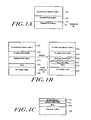
- FIGS. 1A-1Care block diagrams showing the process of producing a SGOI substrate in accordance with the invention.
- FIGS. 2A and 2Bare infrared transmission images of an as-bonded wafer pair and a final SGOI substrate after splitting, respectively;
- FIG. 3is a TEM cross-section view of a SiGe layer that was transferred onto the top of a buried oxide
- FIG. 4is an AFM for a transferred SGOI substrate showing surface roughness
- FIGS. 5-8are block diagrams of various exemplary embodiments semiconductor structures in accordance with the invention.
- heteroepitaxial SiGe layersare formed by a graded epitaxial growth technology.
- a linearly stepwise compositionally graded Si 1-x Ge x buffer 102is deposited with CVD, by increasing Ge concentration from zero to 25%.
- a 2.5 ⁇ m relaxed Si 0.75 Ge 0.25 cap layer 104is deposited with the final Ge composition, as shown in FIG. 1 A.
- the relaxed SiGe cap layerhas high quality with very low dislocation defect density (less than 1E6/cm 2 ), as the graded buffer accommodates the lattice mismatch between Si and relaxed SiGe. A thin layer of this high quality SiGe will be transferred into the final SGOI structure.
- the surface of the as-grown relaxed SiGe layershows a high roughness around 11 nm to 15 nm due to the underlying strain fields generated by misfit dislocations at the graded layer interfaces and thus chemical-mechanical polishing (CMP) is used to smooth the surface.
- CMPchemical-mechanical polishing
- the donor waferis implanted with hydrogen ion (100 keV, 5E16 H + /cm 2 ) to form a buried hydrogen-rich layer. After a surface clean step in a modified RCA solution, it is bonded to an oxidized 106 Si handle wafer 108 at room temperature as shown in FIG. 1 B.
- the wafer bondingis one of the key steps, and the bonding energy should be strong enough in order to sustain the subsequent layer transfer in the next step.
- Good bondingrequires a flat surface and a highly hydrophilic surface before bonding.
- the buried oxide in the final bonded structureis also required to have good electrical properties as it will influence the final device fabricated on it.
- thermal oxide on the donor waferis commonly used before H + implantation and wafer bonding, which becomes the buried oxide in the resulting silicon-on-insulator structure.
- the thermal oxide of the Si donor wafermeets all the requirements, as it has good electrical properties, has flat surface and bonds very well to the handle wafer. Unlike the Si, however, the oxidation of SiGe film results in poor thermal oxide quality, and the Ge segregation during oxidation also degrades the SiGe film. Therefore the thermal oxide of SiGe is not suitable for the SGOI fabrication. In one exemplary experiment the SiGe film will be directly bonded to an oxidized Si handle wafer. The high quality thermal oxide in the handle wafer will become the buried oxide in the final SGOI structure.
- the SiGe waferwent through a clean step.
- one difficulty of SiGe filmis that, SiGe surface becomes rougher during the standard RCA clean, as the NH 4 OH in RCA 1 solution etches Ge faster than Si. Rough surface will lead to weak bonding as the contact area is reduced when bonded to the handle wafer.
- H 2 SO 4 —H 2 O 2 solutionis used in the place of RCA 1 , which also meets the clean process requirement for the subsequent furnace annealing after bonding.
- the SiGe surface after H 2 SO 4 —H 2 O 2 cleanshows better surface roughness compared to RCA 1 .
- the SiGe waferis dipped in the diluted HF solution to remove the old native oxide. It is then rinsed in DI water thoroughly to make the surface hydrophilic by forming a fresh new native oxide layer that is highly active.
- the SiGe waferis bonded to an oxidized handle wafer at room temperature, and then annealed at 600° C. for 3 hours. During anneal the bonded pair split into two sheets along the buried hydrogen-rich layer, and a thin relaxed Si 0.75 Ge 0.25 film 110 is transferred into the handle wafer, resulting in a SGOI substrate 112 , as shown in FIG. 1B. A final 850° C. anneal improves the Si 0.75 Ge 0.25 /SiO 2 bond. Thereafter, device layers 114 can be processed on the SGOI substrate 112 as shown in FIG. 1 C.
- FIGS. 2A and 2Bare infrared transmission images of the as-bonded wafer pair and the final SGOI substrate after splitting, respectively.
- TEMtransmission electron microscopy
- AFMatomic force microscopy
- the TEM cross-section view in FIG. 3shows a ⁇ 640 nm SiGe layer was transferred onto the top of a 550 nm buried oxide (BOX). Surface damage is also shown clearly at the splitting surface with a damage depth of ⁇ 100 nm.
- FIG. 4shows a surface roughness of 11.3 nm in an area of 5 ⁇ 5 ⁇ m 2 by AFM for the as-transferred SGOI.
- the datais similar to those from as-transferred silicon film by smart-cut process, and suggests that a top layer of about 100 nm should be removed by a final CMP step.
- SiGe film transferringonly a thin relaxed SiGe film is removed and the donor wafer can be used again for a donor wafer.
- various device structurescan be realized by growing one or more device layers on the top, as shown in FIG. 2 C. Electrical evaluation is in progress by growing a strain Si layer on the top of this SGOI substrate followed by fabrication of strained Si channel devices.
- Bond strengthis important to the process of the invention.
- AFM measurementswere conducted to investigate the SiGe film surface roughness before bonding under different conditions.
- One experimentis designed to investigate how long the SiGe surface should be polished to have smooth surface and good bond strength, since the surface of the as-grown relaxed SiGe layer has a high roughness around 11 nm to 15 nm.
- Several identical 4-inch Si wafers with relaxed Si 0.75 Ge 0.25 filmswere CMPed with optimized polishing conditions for different times.
- the measured surface mircoroughness RMS at an area of 10 ⁇ m ⁇ 10 ⁇ mis 5.5 ⁇ , 4.5 ⁇ and 3.8 ⁇ , for wafer CMPed for 2 min., 4 min. and 6 min. respectively.
- the tested bond strengthincreases with decreasing RMS.
- a CMP time of 6 min.is necessary for good strength.
- the wafer after H 2 SO 4 :H 2 O 2 solutionshows a surface roughness RMS of 2 ⁇ at an area of 1 ⁇ m ⁇ 1 ⁇ m, which after NH 4 OH:H 2 O 2 :H 2 O shows 4.4 ⁇ .
- the conventional RCA cleanroughens the SiGe surface significantly, and H 2 SO 4 :H 2 O 2 should be used for SiGe clean.
- the clean procedureis optimized before bonding.
- SiGe-oxide bondingFor direct SiGe wafer to oxidized handle wafer bonding (SiGe-oxide bonding), several different clean procedures were tested. It has been found that the H 2 SO 4 :H 2 O 2 (2 ⁇ 4:1) solution followed by DI water rinse and spin dry gives good bond strength. Alternatively, one can also deposit an oxide layer on the SiGe wafer and then CMP the oxide layer. In this case SiGe/oxide is bonded to an oxidized handle wafer, i.e. oxide-oxide bonding.
- NH 4 OH:H 2 O 2 :H 2 O clean and DI water rinse following by diluted HF, DI water rinse and spin drygives very good bond strength.
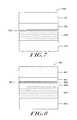
- FIG. 5is a block diagram of an exemplary embodiment of a semiconductor structure 500 in accordance with the invention.
- a graded Si 1-x Ge x buffer layer 504is grown on a silicon substrate 502 , where the Ge concentration x is increased from zero to a value y in a stepwise manner, and y has a selected value between 0 and 1.
- a second relaxed Si 1-y Ge y layer 506is then deposited, and hydrogen ions are implanted into this layer with a selected depth by adjusting implantation energy, forming a buried hydrogen-rich layer 508 .
- the waferis cleaned and bonded to an oxidized handle wafer 510 .
- An anneal treatment at 500 ⁇ 600° C.splits the bonded pair at the hydrogen-rich layer 508 .
- the upper portion of the relaxed Si 1-y Ge y layer 506remains on the oxidized handle wafer, forming a SGOI substrate.
- the standard RCA clean for the silicon surfaceis modified. Since the NH 4 OH in standard RCA 1 solution etches Ge faster than Si, the SiGe surface will become rough, leading to a weak bond. A H 2 SO 4 —H 2 O 2 solution is used in the place of RCA 1 , which also meets the clean process requirement for the subsequent furnace annealing after bonding. The SiGe surface after the H 2 SO 4 —H 2 O 2 clean showed better surface roughness compared to RCA 1 .
- the wafersare then immersed in another fresh H 2 SO 4 —H 2 O 2 solution for 10 to 20 min. H 2 SO 4 —H 2 O 2 renders the SiGe surface hydrophilic. After a rinse in DI wafer and spin drying, the SiGe wafer is bonded to an oxidized handle wafer at room temperature immediately, and then annealed at 500 ⁇ 600° C. for wafer splitting.
- FIG. 6is a block diagram of another exemplary embodiment of a semiconductor structure 600 .
- the structure 600includes a graded Si 1-x Ge x buffer layer 604 grown on a silicon substrate 602 , where the Ge concentration x is increased from zero to 1. Then a relaxed pure Ge layer 606 and a III-V material layer 608 , such as a GaAs layer, are epitaxially grown on the Ge layer. Hydrogen ions are implanted into the GaAs layer 608 with a selected depth by adjusting implantation energy, forming a buried hydrogen-rich layer 610 . The wafer is cleaned and bonded to an oxidized handle wafer 612 . An anneal treatment splits the bonded pair at the hydrogen-rich layer 610 . As a result, the upper portion of the GaAs layer 608 remains on the oxidized handle wafer, forming a GaAs-on-insulator substrate.
- FIG. 7is a block diagram of yet another exemplary embodiment of a semiconductor structure 700 .
- a graded Si 1-x Ge x buffer layer 704is grown on a silicon substrate 702 , where the Ge concentration x is increased from zero to a selected value y, where is less than 0.2.
- a second relaxed Si 1-z Ge z layer 706is deposited, where z is between 0.2 to 0.25.
- Hydrogen ionsare implanted into the graded Si 1-x Ge x buffer layer 704 with a selected depth, forming a buried hydrogen-rich layer 708 within layer 704 .
- the waferis cleaned and bonded to an oxidized handle wafer 710 .
- An anneal treatment at 500 ⁇ 600° C.splits the bonded pair at the hydrogen-rich layer 708 .
- the upper portion of the graded Si 1-x Ge x buffer layer 704 and the relaxed Si 1-z Ge z layer 706remains on the oxidized handle wafer 710 .
- the remaining graded Si 1-x Ge x buffer layer 704is then selectively etched by either KOH or TMAH. KOH and TMAH etch Si 1-x Ge x fast when x is less 0.2, but becomes very slow when x is larger than 0.2.
- the graded Si 1-x Ge x buffer layer 704can be etched selectively, leaving the relaxed Si 1-z Ge z layer 706 on the insulating substrate 710 and forming a relaxed SGOI substrate.
- the thickness of the relaxed Si 1-z Ge z film 706 on the final SGOI structureis defined by film growth, which is desired in some applications.
- FIG. 8is a block diagram of yet another exemplary embodiment of a semiconductor structure 800 .
- a graded Si 1-x Ge x buffer layer 804is grown on a silicon substrate 802 , where the Ge concentration x is increased from zero to a selected value y between 0 and 1.
- a second relaxed Si 1-y Ge y layer 806is deposited, followed by a strained Si 1-z Ge z layer 808 and another relaxed Si 1-y Ge y layer 810 .
- the thickness of layers 806 , 808 , and 810 , and the value zare chosen such that the Si 1-z Ge z layer 808 is under equilibrium strain state while the Si 1-y Ge y layers 806 and 810 remain relaxed.
- hydrogen ionsmay be introduced into the strained Si 1-z Ge z layer 808 , forming a hydrogen-rich layer 812 .
- the waferis cleaned and bonded to an oxidized handle wafer 814 .
- the bonded pairis then separated along the strained Si 1-z Ge z layer 808 .
- the crackpropagates along this layer during separation.
- the separationcan be accomplished by a variety of techniques, for example using a mechanical force or an anneal treatment at 500 ⁇ 600° C. when the hydrogen is also introduced. See, for example, U.S. Pat. Nos. 6,033,974 and 6,184,111, both of which are incorporated herein by reference.
- the relaxed Si 1-y Ge y layer 810remains on the oxidized handle wafer, forming a relaxed SGOI substrate.
- the thickness of layers 806 , 808 , and 810 , and the value zmay also be chosen such that there are a good amount of dislocations present in the Si 1-z Ge z layer 808 while the top Si 1-y Ge y layer 810 remains relaxed and having high quality and limited dislocation defects.
- the hydrogen ionsmay be introduced by various ways, such as ion implantation or ion diffusion or drift by means of electrolytic charging.
- the value of zmay be chosen in such a way that the remaining Si 1-z Ge z layer 808 can be etched selectively by KOH or TMAH.
- the layers 806 and 810may also be some other materials, for example pure Ge, or some III-V materials, under the condition that the Ge concentration x in the graded Si 1-x Ge x buffer layer 804 is increased from zero to 1.
- CMPmaybe used to polish the surface.
Landscapes
- Engineering & Computer Science (AREA)
- Physics & Mathematics (AREA)
- Condensed Matter Physics & Semiconductors (AREA)
- General Physics & Mathematics (AREA)
- Manufacturing & Machinery (AREA)
- Computer Hardware Design (AREA)
- Microelectronics & Electronic Packaging (AREA)
- Power Engineering (AREA)
- Chemical & Material Sciences (AREA)
- Materials Engineering (AREA)
- Recrystallisation Techniques (AREA)
- Element Separation (AREA)
Abstract
Description
This application is a continuation of application Ser. No. 10/384,160, filed Mar. 7, 2003, now U.S. Pat. No. 6,737,670 that is a divisional of application Ser. No. 09/928,126, filed on Aug. 10, 2001, issued as U.S. Pat. No. 6,573,126 on Jun. 3, 2003, which claims priority from provisional application Ser. No. 60/225,666, filed Aug. 16, 2000, now expired, the entire disclosures of which are incorporated by reference herein.
The present invention relates to a production of a general substrate of relaxed Si1-xGex-on-insulator (SGOI) for various electronics or optoelectronics applications, and the production of monocrystalline III-V or II-VI material-on-insulator substrate.
Relaxed Si1-xGex-on-insulator (SGOI) is a very promising technology as it combines the benefits of two advanced technologies: the conventional SOI technology and the disruptive SiGe technology. The SOI configuration offers various advantages associated with the insulating substrate, namely reduced parasitic capacitances, improved isolation, reduced short-channel-effect, etc. High mobility strained-Si, strained-Si1-xGexor strained-Ge MOS devices can be made on SGOI substrates.
Other III-V optoelectronic devices can also be integrated into the SGOI substrate by matching the lattice constants of III-V materials and the relaxed Si1-xGex. For example a GaAs layer can be grown on Si1-xGex-on-insulator where x is equal or close to 1. SGOI may serve as an ultimate platform for high speed, low power electronic and optoelectronic applications.
SGOI has been fabricated by several methods in the prior art. In one method, the separation by implantation of oxygen (SIMOX) technology is used to produce SGOI. High dose oxygen implant was used to bury high concentrations of oxygen in a Si1-xGexlayer, which was then converted into a buried oxide (BOX) layer upon annealing at high temperature (for example, 1350° C.). See, for example, Mizuno et al. IEEE Electron Device Letters, Vol. 21, No. 5, pp. 230-232, 2000 and Ishilawa et al. Applied Physics Letters, Vol. 75, No. 7, pp. 983-985, 1999. One of the main drawbacks is the quality of the resulting Si1-xGexfilm and BOX. In addition, Ge segregation during high temperature anneal also limits the maximum Ge composition to a low value.
U.S. Pat. Nos. 5,461,243 and 5,759,898 describe a second method, in which a conventional silicon-on-insulator (SOI) substrate was used as a compliant substrate. In the process, an initially strained Si1-xGexlayer was deposited on a thin SOI substrate. Upon an anneal treatment, the strain was transferred to the thin silicon film underneath, resulting in relaxation of the top Si1-xGexfilm. The final structure is relaxed-SiGe/strained-Si/insulator, which is not an ideal SGOI structure. The silicon layer in the structure is unnecessary, and may complicate or undermine the performance of devices built on it. For example, it may form a parasitic back channel on this strained-Si, or may confine unwanted electrons due to the band gap offset between the strained-Si and SiGe layer.
U.S. Pat. Nos. 5,906,951 and 6,059,895 describe the formation of a similar SGOI structure: strained-layer(s)/relaxed-SiGe/Si/insulator structure. The structure was produced by wafer bonding and etch back process using a P++ layer as an etch stop. The presence of the silicon layer in the above structure may be for the purpose of facilitating Si-insulator wafer bonding, but is unnecessary for ideal SGOI substrates. Again, the silicon layer may also complicate or undermine the performance of devices built on it. For example, it may form a parasitic back channel on this strained-Si, or may confine unwanted electrons due to the band gap offset between the strained-Si and SiGe layer. Moreover, the etch stop of P++ in the above structure is not practical when the first graded Si1-yGeylayer described in the patents has a y value of larger than 0.2. Experiments from research shows Si1-yGeywith y larger than 0.2 is a very good etch stop for both KOH and TMAH, as described in a published PCT application WO 99/53539. Therefore, the KOH will not be able to remove the first graded Si1-yGeylayer and the second relaxed SiGe layer as described in the patents.
Other attempts include re-crystallization of an amorphous Si1-xGexlayer deposited on the top of SOI (silicon-on-insulator) substrate, which is again not an ideal SGOI substrate and the silicon layer is unnecessary, and may complicate or undermine the performance of devices built on it. Note Yeo et al. IEEE Electron Device Letters, Vol. 21, No. 4, pp. 161-163, 2000. The relaxation of the resultant SiGe film and quality of the resulting structure are main concerns.
From the above, there is a need for a simple technique for relaxed SGOI substrate production, a need for a technique for production of high quality SGOI and other III-V material-on-insulator, and a need for a technique for wide range of material transfer.
According to the invention, there is provided an improved technique for production of wide range of high quality material is provided. In particular, the production of relaxed Si1-xGex-on-insulator (SGOI) substrate or relaxed III-V or II-VI material-on-insulator, such as GaAs-on-insulator, is described. High quality monocrystalline relaxed SiGe layer, relaxed Ge layer, or other relaxed III-V material layer is grown on a silicon substrate using a graded Si1-xGexepitaxial growth technique. A thin film of the layer is transferred into an oxidized handle wafer by wafer bonding and wafer splitting using hydrogen ion implantation. The invention makes use of the graded Si1-xGexbuffer structure, resulting in a simplified and improved process.
The invention also provides a method allowing a wide range of device materials to be integrated into the inexpensive silicon substrate. For example, it allows production of Si1-xGex-on-insulator with wide range of Ge concentration, and allows production of many III-V or II-VI materials on insulator like GaAs, AlAs, ZnSe and InGaP. The use of graded Si1-xGexbuffer in the invention allows high quality materials with limited dislocation defects to be produced and transferred. In one example, SGOI is produced using a SiGe structure in which a region in the graded buffer can act as a natural etch stop.
The invention provides a process and method for producing monocrystalline semiconductor layers. In an exemplary embodiment, a graded Si1-xGex(x increases from 0 to y) is deposited on a first silicon substrate, followed by deposition of a relaxed Si1-yGeylayer, a thin strained Si1-zGezlayer and another relaxed Si1-yGeylayer. Hydrogen ions are then introduced into the strained Si1-zGezlayer. The relaxed Si1-yGeylayer is bonded to a second oxidized substrate. An annealing treatment splits the bonded pair at the strained Si layer, whereby the second relaxed Si1-yGeylayer remains on said second substrate.
In another exemplary embodiment, a graded Si1-xGexis deposited on a first silicon substrate, where the Ge concentration x is increased from 0 to 1. Then a relaxed GaAs layer is deposited on the relaxed Ge buffer. As the lattice constant of GaAs is close to that of Ge, GaAs has high quality with limited dislocation defects. Hydrogen ions are introduced into the relaxed GaAs layer at the selected depth. The relaxed GaAs layer is bonded to a second oxidized substrate. An annealing treatment splits the bonded pair at the hydrogen ion rich layer, whereby the upper portion of relaxed GaAs layer remains on said second substrate.
An example of a process in which SGOI is created by layer transfer is described. The experiment was performed in two stages. In the first stage, heteroepitaxial SiGe layers are formed by a graded epitaxial growth technology. Starting with a 4-inch Si (100)donor wafer 100, a linearly stepwise compositionally graded Si1-xGexbuffer102 is deposited with CVD, by increasing Ge concentration from zero to 25%. Then a 2.5 μm relaxed Si0.75Ge0.25cap layer104 is deposited with the final Ge composition, as shown in FIG.1A.
The relaxed SiGe cap layer has high quality with very low dislocation defect density (less than 1E6/cm2), as the graded buffer accommodates the lattice mismatch between Si and relaxed SiGe. A thin layer of this high quality SiGe will be transferred into the final SGOI structure. The surface of the as-grown relaxed SiGe layer shows a high roughness around 11 nm to 15 nm due to the underlying strain fields generated by misfit dislocations at the graded layer interfaces and thus chemical-mechanical polishing (CMP) is used to smooth the surface. In the second stage, the donor wafer is implanted with hydrogen ion (100 keV, 5E16 H+/cm2) to form a buried hydrogen-rich layer. After a surface clean step in a modified RCA solution, it is bonded to an oxidized106Si handle wafer 108 at room temperature as shown in FIG.1B.
The wafer bonding is one of the key steps, and the bonding energy should be strong enough in order to sustain the subsequent layer transfer in the next step. Good bonding requires a flat surface and a highly hydrophilic surface before bonding. On the other hand, the buried oxide in the final bonded structure is also required to have good electrical properties as it will influence the final device fabricated on it. In the conventional Si film transfer, thermal oxide on the donor wafer is commonly used before H+ implantation and wafer bonding, which becomes the buried oxide in the resulting silicon-on-insulator structure.
The thermal oxide of the Si donor wafer meets all the requirements, as it has good electrical properties, has flat surface and bonds very well to the handle wafer. Unlike the Si, however, the oxidation of SiGe film results in poor thermal oxide quality, and the Ge segregation during oxidation also degrades the SiGe film. Therefore the thermal oxide of SiGe is not suitable for the SGOI fabrication. In one exemplary experiment the SiGe film will be directly bonded to an oxidized Si handle wafer. The high quality thermal oxide in the handle wafer will become the buried oxide in the final SGOI structure.
Having a flat surface after a CMP step, the SiGe wafer went through a clean step. Compared to Si, one difficulty of SiGe film is that, SiGe surface becomes rougher during the standard RCA clean, as the NH4OH in RCA1 solution etches Ge faster than Si. Rough surface will lead to weak bonding as the contact area is reduced when bonded to the handle wafer. In this exemplary embodiment, H2SO4—H2O2solution is used in the place of RCA1, which also meets the clean process requirement for the subsequent furnace annealing after bonding. The SiGe surface after H2SO4—H2O2clean shows better surface roughness compared to RCA1.
After this modified clean procedure, the SiGe wafer is dipped in the diluted HF solution to remove the old native oxide. It is then rinsed in DI water thoroughly to make the surface hydrophilic by forming a fresh new native oxide layer that is highly active. After spinning dry, the SiGe wafer is bonded to an oxidized handle wafer at room temperature, and then annealed at 600° C. for 3 hours. During anneal the bonded pair split into two sheets along the buried hydrogen-rich layer, and a thin relaxed Si0.75Ge0.25film110 is transferred into the handle wafer, resulting in aSGOI substrate 112, as shown inFIG. 1B. A final 850° C. anneal improves the Si0.75Ge0.25/SiO2bond. Thereafter, device layers114 can be processed on theSGOI substrate 112 as shown in FIG.1C.
Bond strength is important to the process of the invention. AFM measurements were conducted to investigate the SiGe film surface roughness before bonding under different conditions. One experiment is designed to investigate how long the SiGe surface should be polished to have smooth surface and good bond strength, since the surface of the as-grown relaxed SiGe layer has a high roughness around 11 nm to 15 nm. Several identical 4-inch Si wafers with relaxed Si0.75Ge0.25films were CMPed with optimized polishing conditions for different times. Using AFM, the measured surface mircoroughness RMS at an area of 10 μm×10 μm is 5.5 Å, 4.5Å and 3.8 Å, for wafer CMPed for 2 min., 4 min. and 6 min. respectively. After bonding to identical handle wafers, the tested bond strength increases with decreasing RMS. A CMP time of 6 min. is necessary for good strength.
In another experiment, two identical 4-inch Si wafers with relaxed Si0.75Ge0.25films were CMPed for 8 min. After two cleaning steps in H2SO4:H2O2solution and one step in diluted HF solution, one wafer was put in a new H2SO4:H2O2(3:1) solution and another in a new NH4OH:H2O2:H2O (1:1:5), i.e. the conventional RCA1 solution, both for 15 min. The resultant wafers were tested using AFM. The wafer after H2SO4:H2O2solution shows a surface roughness RMS of 2 Å at an area of 1 μm×1 μm, which after NH4OH:H2O2:H2O shows 4.4 Å. Clearly, the conventional RCA clean roughens the SiGe surface significantly, and H2SO4:H2O2should be used for SiGe clean.
In yet another experiment, the clean procedure is optimized before bonding. For direct SiGe wafer to oxidized handle wafer bonding (SiGe-oxide bonding), several different clean procedures were tested. It has been found that the H2SO4:H2O2(2˜4:1) solution followed by DI water rinse and spin dry gives good bond strength. Alternatively, one can also deposit an oxide layer on the SiGe wafer and then CMP the oxide layer. In this case SiGe/oxide is bonded to an oxidized handle wafer, i.e. oxide-oxide bonding. Among different clean procedures, it was found that NH4OH:H2O2:H2O clean and DI water rinse following by diluted HF, DI water rinse and spin dry gives very good bond strength.
During the wafer clean step prior to bonding, the standard RCA clean for the silicon surface is modified. Since the NH4OH in standard RCA1 solution etches Ge faster than Si, the SiGe surface will become rough, leading to a weak bond. A H2SO4—H2O2solution is used in the place of RCA1, which also meets the clean process requirement for the subsequent furnace annealing after bonding. The SiGe surface after the H2SO4—H2O2clean showed better surface roughness compared to RCA1. After the modified RCA clean, the wafers are then immersed in another fresh H2SO4—H2O2solution for 10 to 20 min. H2SO4—H2O2renders the SiGe surface hydrophilic. After a rinse in DI wafer and spin drying, the SiGe wafer is bonded to an oxidized handle wafer at room temperature immediately, and then annealed at 500˜600° C. for wafer splitting.
As a result, the upper portion of the graded Si1-xGexbuffer layer704 and the relaxed Si1-zGezlayer706 remains on the oxidizedhandle wafer 710. The remaining graded Si1-xGexbuffer layer704 is then selectively etched by either KOH or TMAH. KOH and TMAH etch Si1-xGexfast when x is less 0.2, but becomes very slow when x is larger than 0.2. Thus, the graded Si1-xGexbuffer layer704 can be etched selectively, leaving the relaxed Si1-zGezlayer706 on the insulatingsubstrate 710 and forming a relaxed SGOI substrate. In this process, the thickness of the relaxed Si1-zGezfilm706 on the final SGOI structure is defined by film growth, which is desired in some applications.
Since the strain makes the layer weaker, the crack propagates along this layer during separation. The separation can be accomplished by a variety of techniques, for example using a mechanical force or an anneal treatment at 500˜600° C. when the hydrogen is also introduced. See, for example, U.S. Pat. Nos. 6,033,974 and 6,184,111, both of which are incorporated herein by reference. As a result, the relaxed Si1-yGeylayer810 remains on the oxidized handle wafer, forming a relaxed SGOI substrate. The thickness oflayers
These dislocation defects in the Si1-zGezlayer808 can then act as hydrogen trap centers during the subsequent step of introducing ions. The hydrogen ions may be introduced by various ways, such as ion implantation or ion diffusion or drift by means of electrolytic charging. The value of z may be chosen in such a way that the remaining Si1-zGezlayer808 can be etched selectively by KOH or TMAH. Thelayers
After all the semiconductor-on-insulator substrate obtained by the approaches described above, various device layers can be further grown on the top. Before the regrowth, CMP maybe used to polish the surface.
Although the present invention has been shown and described with respect to several preferred embodiments thereof, various changes, omissions and additions to the form and detail thereof, may be made therein, without departing from the spirit and scope of the invention.
Claims (9)
1. A semiconductor structure comprising:
a substrate including an insulator layer; and
a device layer disposed over the insulator layer, the device layer comprising at least one of strained Si, strained Si1-wGew, strained Ge, GaAs, AlAs, ZnSe, and InGaP.
2. The structure ofclaim 1 wherein a surface of the structure has a root mean square surface roughness of less than about 11 nanometers.
3. The structure ofclaim 1 , further comprising:
a device integrated into at least a portion of the device layer.
4. The semiconductor structure ofclaim 1 , wherein the substrate comprises silicon.
5. A semiconductor structure comprising:
a substrate comprising silicon;
an insulating layer disposed over the substrate; and
a relaxed Si1-yGeylayer disposed over and in contact with the insulating layer,
wherein a Ge concentration y of the relaxed layer is selected from the range of greater than zero to 1.
6. The structure ofclaim 5 wherein the Ge concentration y has a value of 1.
7. The structure ofclaim 5 , further comprising:
a device disposed within at least a portion of the relaxed Si1-yGeylayer.
8. The structure ofclaim 1 , wherein the device layer comprises strained Si1-wGew.
9. The structure ofclaim 1 , wherein the device layer comprises strained Ge.
Priority Applications (1)
| Application Number | Priority Date | Filing Date | Title |
|---|---|---|---|
| US10/802,185US6921914B2 (en) | 2000-08-16 | 2004-03-17 | Process for producing semiconductor article using graded epitaxial growth |
Applications Claiming Priority (4)
| Application Number | Priority Date | Filing Date | Title |
|---|---|---|---|
| US22566600P | 2000-08-16 | 2000-08-16 | |
| US09/928,126US6573126B2 (en) | 2000-08-16 | 2001-08-10 | Process for producing semiconductor article using graded epitaxial growth |
| US10/384,160US6737670B2 (en) | 2000-08-16 | 2003-03-07 | Semiconductor substrate structure |
| US10/802,185US6921914B2 (en) | 2000-08-16 | 2004-03-17 | Process for producing semiconductor article using graded epitaxial growth |
Related Parent Applications (1)
| Application Number | Title | Priority Date | Filing Date |
|---|---|---|---|
| US10/384,160ContinuationUS6737670B2 (en) | 2000-08-16 | 2003-03-07 | Semiconductor substrate structure |
Publications (2)
| Publication Number | Publication Date |
|---|---|
| US20040173791A1 US20040173791A1 (en) | 2004-09-09 |
| US6921914B2true US6921914B2 (en) | 2005-07-26 |
Family
ID=22845751
Family Applications (5)
| Application Number | Title | Priority Date | Filing Date |
|---|---|---|---|
| US09/928,126Expired - LifetimeUS6573126B2 (en) | 2000-08-16 | 2001-08-10 | Process for producing semiconductor article using graded epitaxial growth |
| US10/379,355Expired - LifetimeUS6713326B2 (en) | 2000-08-16 | 2003-03-04 | Process for producing semiconductor article using graded epitaxial growth |
| US10/384,160Expired - Fee RelatedUS6737670B2 (en) | 2000-08-16 | 2003-03-07 | Semiconductor substrate structure |
| US10/802,185Expired - LifetimeUS6921914B2 (en) | 2000-08-16 | 2004-03-17 | Process for producing semiconductor article using graded epitaxial growth |
| US10/802,186AbandonedUS20050009288A1 (en) | 2000-08-16 | 2004-03-17 | Process for producing semiconductor article using graded epitaxial growth |
Family Applications Before (3)
| Application Number | Title | Priority Date | Filing Date |
|---|---|---|---|
| US09/928,126Expired - LifetimeUS6573126B2 (en) | 2000-08-16 | 2001-08-10 | Process for producing semiconductor article using graded epitaxial growth |
| US10/379,355Expired - LifetimeUS6713326B2 (en) | 2000-08-16 | 2003-03-04 | Process for producing semiconductor article using graded epitaxial growth |
| US10/384,160Expired - Fee RelatedUS6737670B2 (en) | 2000-08-16 | 2003-03-07 | Semiconductor substrate structure |
Family Applications After (1)
| Application Number | Title | Priority Date | Filing Date |
|---|---|---|---|
| US10/802,186AbandonedUS20050009288A1 (en) | 2000-08-16 | 2004-03-17 | Process for producing semiconductor article using graded epitaxial growth |
Country Status (5)
| Country | Link |
|---|---|
| US (5) | US6573126B2 (en) |
| EP (1) | EP1309989B1 (en) |
| JP (2) | JP2004507084A (en) |
| DE (1) | DE60125952T2 (en) |
| WO (1) | WO2002015244A2 (en) |
Cited By (27)
| Publication number | Priority date | Publication date | Assignee | Title |
|---|---|---|---|---|
| US20060083280A1 (en)* | 2004-10-19 | 2006-04-20 | Commissariat A L'energie Atomique | Method for producing multilayers on a substrate |
| US20060099773A1 (en)* | 2004-11-10 | 2006-05-11 | Sharp Laboratories Of America, Inc. | Fabrication of a low defect germanium film by direct wafer bonding |
| US7060632B2 (en) | 2002-03-14 | 2006-06-13 | Amberwave Systems Corporation | Methods for fabricating strained layers on semiconductor substrates |
| US20060197124A1 (en)* | 2002-06-07 | 2006-09-07 | Amberwave Systems Corporation | Double gate strained-semiconductor-on-insulator device structures |
| US7259388B2 (en) | 2002-06-07 | 2007-08-21 | Amberwave Systems Corporation | Strained-semiconductor-on-insulator device structures |
| US20080006854A1 (en)* | 2006-06-21 | 2008-01-10 | International Business Machines Corporation | Mosfets comprising source/drain regions with slanted upper surfaces, and method for fabricating the same |
| US20080081485A1 (en)* | 2005-06-15 | 2008-04-03 | Papanu James S | Post-ion implant cleaning on silicon on insulator substrate preparation |
| US7393733B2 (en) | 2004-12-01 | 2008-07-01 | Amberwave Systems Corporation | Methods of forming hybrid fin field-effect transistor structures |
| US20100003828A1 (en)* | 2007-11-28 | 2010-01-07 | Guowen Ding | Methods for adjusting critical dimension uniformity in an etch process with a highly concentrated unsaturated hydrocarbon gas |
| US20110193195A1 (en)* | 2009-12-17 | 2011-08-11 | Atwater Harry A | Virtual substrates for epitaxial growth and methods of making the same |
| WO2011126528A1 (en)* | 2010-04-08 | 2011-10-13 | California Institute Of Technology | Virtual substrates for epitaxial growth and methods of making the same |
| US8124470B1 (en) | 2010-09-29 | 2012-02-28 | International Business Machines Corporation | Strained thin body semiconductor-on-insulator substrate and device |
| US20130075725A1 (en)* | 2011-09-27 | 2013-03-28 | Taiwan Semiconductor Manufacturing Company, Ltd. | Enhanced wafer test line structure |
| US8466036B2 (en) | 2010-12-24 | 2013-06-18 | Io Semiconductor, Inc. | Trap rich layer for semiconductor devices |
| US8481405B2 (en) | 2010-12-24 | 2013-07-09 | Io Semiconductor, Inc. | Trap rich layer with through-silicon-vias in semiconductor devices |
| US8536021B2 (en) | 2010-12-24 | 2013-09-17 | Io Semiconductor, Inc. | Trap rich layer formation techniques for semiconductor devices |
| US8748292B2 (en) | 2002-06-07 | 2014-06-10 | Taiwan Semiconductor Manufacturing Company, Ltd. | Methods of forming strained-semiconductor-on-insulator device structures |
| US20140220765A1 (en)* | 2011-10-18 | 2014-08-07 | Fuji Electric Co., Ltd. | Method for separating support substrate from solid-phase bonded wafer and method for manufacturing semiconductor device |
| US9466672B1 (en) | 2015-11-25 | 2016-10-11 | International Business Machines Corporation | Reduced defect densities in graded buffer layers by tensile strained interlayers |
| US9553013B2 (en) | 2010-12-24 | 2017-01-24 | Qualcomm Incorporated | Semiconductor structure with TRL and handle wafer cavities |
| US9570300B1 (en)* | 2016-02-08 | 2017-02-14 | International Business Machines Corporation | Strain relaxed buffer layers with virtually defect free regions |
| US9624096B2 (en) | 2010-12-24 | 2017-04-18 | Qualcomm Incorporated | Forming semiconductor structure with device layers and TRL |
| US9754860B2 (en) | 2010-12-24 | 2017-09-05 | Qualcomm Incorporated | Redistribution layer contacting first wafer through second wafer |
| US20180019169A1 (en)* | 2016-07-12 | 2018-01-18 | QMAT, Inc. | Backing substrate stabilizing donor substrate for implant or reclamation |
| US9922941B1 (en) | 2016-09-21 | 2018-03-20 | International Business Machines Corporation | Thin low defect relaxed silicon germanium layers on bulk silicon substrates |
| US10032870B2 (en) | 2015-03-12 | 2018-07-24 | Globalfoundries Inc. | Low defect III-V semiconductor template on porous silicon |
| US10418273B2 (en)* | 2015-10-13 | 2019-09-17 | Nanyang Technological University | Method of manufacturing a germanium-on-insulator substrate |
Families Citing this family (179)
| Publication number | Priority date | Publication date | Assignee | Title |
|---|---|---|---|---|
| JP3535527B2 (en)* | 1997-06-24 | 2004-06-07 | マサチューセッツ インスティテュート オブ テクノロジー | Controlling threading dislocations in germanium-on-silicon using graded GeSi layer and planarization |
| US7227176B2 (en)* | 1998-04-10 | 2007-06-05 | Massachusetts Institute Of Technology | Etch stop layer system |
| US6633066B1 (en)* | 2000-01-07 | 2003-10-14 | Samsung Electronics Co., Ltd. | CMOS integrated circuit devices and substrates having unstrained silicon active layers |
| JP2003520444A (en) | 2000-01-20 | 2003-07-02 | アンバーウェーブ システムズ コーポレイション | Low threading dislocation density lattice-mismatched epilayer that does not require high-temperature growth |
| US6750130B1 (en) | 2000-01-20 | 2004-06-15 | Amberwave Systems Corporation | Heterointegration of materials using deposition and bonding |
| US6602613B1 (en) | 2000-01-20 | 2003-08-05 | Amberwave Systems Corporation | Heterointegration of materials using deposition and bonding |
| AU2001263211A1 (en) | 2000-05-26 | 2001-12-11 | Amberwave Systems Corporation | Buried channel strained silicon fet using an ion implanted doped layer |
| US6573126B2 (en) | 2000-08-16 | 2003-06-03 | Massachusetts Institute Of Technology | Process for producing semiconductor article using graded epitaxial growth |
| US6890835B1 (en)* | 2000-10-19 | 2005-05-10 | International Business Machines Corporation | Layer transfer of low defect SiGe using an etch-back process |
| US6649480B2 (en)* | 2000-12-04 | 2003-11-18 | Amberwave Systems Corporation | Method of fabricating CMOS inverter and integrated circuits utilizing strained silicon surface channel MOSFETs |
| US20020100942A1 (en)* | 2000-12-04 | 2002-08-01 | Fitzgerald Eugene A. | CMOS inverter and integrated circuits utilizing strained silicon surface channel MOSFETs |
| US6703688B1 (en) | 2001-03-02 | 2004-03-09 | Amberwave Systems Corporation | Relaxed silicon germanium platform for high speed CMOS electronics and high speed analog circuits |
| US6723661B2 (en)* | 2001-03-02 | 2004-04-20 | Amberwave Systems Corporation | Relaxed silicon germanium platform for high speed CMOS electronics and high speed analog circuits |
| US6830976B2 (en) | 2001-03-02 | 2004-12-14 | Amberwave Systems Corproation | Relaxed silicon germanium platform for high speed CMOS electronics and high speed analog circuits |
| US6724008B2 (en) | 2001-03-02 | 2004-04-20 | Amberwave Systems Corporation | Relaxed silicon germanium platform for high speed CMOS electronics and high speed analog circuits |
| WO2002082514A1 (en) | 2001-04-04 | 2002-10-17 | Massachusetts Institute Of Technology | A method for semiconductor device fabrication |
| US20050026432A1 (en)* | 2001-04-17 | 2005-02-03 | Atwater Harry A. | Wafer bonded epitaxial templates for silicon heterostructures |
| AU2002322105A1 (en) | 2001-06-14 | 2003-01-02 | Amberware Systems Corporation | Method of selective removal of sige alloys |
| US7301180B2 (en) | 2001-06-18 | 2007-11-27 | Massachusetts Institute Of Technology | Structure and method for a high-speed semiconductor device having a Ge channel layer |
| WO2003001671A2 (en) | 2001-06-21 | 2003-01-03 | Amberwave Systems Corporation | Improved enhancement of p-type metal-oxide-semiconductor field-effect transistors |
| EP1415331A2 (en)* | 2001-08-06 | 2004-05-06 | Massachusetts Institute Of Technology | Formation of planar strained layers |
| US6974735B2 (en) | 2001-08-09 | 2005-12-13 | Amberwave Systems Corporation | Dual layer Semiconductor Devices |
| US7138649B2 (en)* | 2001-08-09 | 2006-11-21 | Amberwave Systems Corporation | Dual-channel CMOS transistors with differentially strained channels |
| US6831292B2 (en)* | 2001-09-21 | 2004-12-14 | Amberwave Systems Corporation | Semiconductor structures employing strained material layers with defined impurity gradients and methods for fabricating same |
| US6933518B2 (en)* | 2001-09-24 | 2005-08-23 | Amberwave Systems Corporation | RF circuits including transistors having strained material layers |
| JP2003205336A (en)* | 2002-01-08 | 2003-07-22 | Tori Techno:Kk | High strength stainless steel bolt and manufacturing method therefor |
| US6805962B2 (en)* | 2002-01-23 | 2004-10-19 | International Business Machines Corporation | Method of creating high-quality relaxed SiGe-on-insulator for strained Si CMOS applications |
| US6746902B2 (en)* | 2002-01-31 | 2004-06-08 | Sharp Laboratories Of America, Inc. | Method to form relaxed sige layer with high ge content |
| US6649492B2 (en)* | 2002-02-11 | 2003-11-18 | International Business Machines Corporation | Strained Si based layer made by UHV-CVD, and devices therein |
| US6793731B2 (en)* | 2002-03-13 | 2004-09-21 | Sharp Laboratories Of America, Inc. | Method for recrystallizing an amorphized silicon germanium film overlying silicon |
| US7132348B2 (en)* | 2002-03-25 | 2006-11-07 | Micron Technology, Inc. | Low k interconnect dielectric using surface transformation |
| GB0209737D0 (en)* | 2002-04-29 | 2002-06-05 | Univ Newcastle | Method of isolating adjacent components of a semiconductor device |
| US7307273B2 (en) | 2002-06-07 | 2007-12-11 | Amberwave Systems Corporation | Control of strain in device layers by selective relaxation |
| AU2003238963A1 (en) | 2002-06-07 | 2003-12-22 | Amberwave Systems Corporation | Semiconductor devices having strained dual channel layers |
| US7335545B2 (en) | 2002-06-07 | 2008-02-26 | Amberwave Systems Corporation | Control of strain in device layers by prevention of relaxation |
| WO2003105189A2 (en)* | 2002-06-07 | 2003-12-18 | Amberwave Systems Corporation | Strained-semiconductor-on-insulator device structures |
| US7615829B2 (en) | 2002-06-07 | 2009-11-10 | Amberwave Systems Corporation | Elevated source and drain elements for strained-channel heterojuntion field-effect transistors |
| US6946371B2 (en) | 2002-06-10 | 2005-09-20 | Amberwave Systems Corporation | Methods of fabricating semiconductor structures having epitaxially grown source and drain elements |
| US6982474B2 (en) | 2002-06-25 | 2006-01-03 | Amberwave Systems Corporation | Reacted conductive gate electrodes |
| US7157119B2 (en) | 2002-06-25 | 2007-01-02 | Ppg Industries Ohio, Inc. | Method and compositions for applying multiple overlying organic pigmented decorations on ceramic substrates |
| US6953736B2 (en) | 2002-07-09 | 2005-10-11 | S.O.I.Tec Silicon On Insulator Technologies S.A. | Process for transferring a layer of strained semiconductor material |
| FR2842350B1 (en)* | 2002-07-09 | 2005-05-13 | METHOD FOR TRANSFERRING A LAYER OF CONCEALED SEMICONDUCTOR MATERIAL | |
| US7510949B2 (en) | 2002-07-09 | 2009-03-31 | S.O.I.Tec Silicon On Insulator Technologies | Methods for producing a multilayer semiconductor structure |
| FR2842349B1 (en) | 2002-07-09 | 2005-02-18 | TRANSFERRING A THIN LAYER FROM A PLATE COMPRISING A BUFFER LAYER | |
| FR2848334A1 (en)* | 2002-12-06 | 2004-06-11 | Soitec Silicon On Insulator | Multi-layer structure production of semiconductor materials with different mesh parameters comprises epitaxy of thin film on support substrate and adhesion on target substrate |
| US7018910B2 (en) | 2002-07-09 | 2006-03-28 | S.O.I.Tec Silicon On Insulator Technologies S.A. | Transfer of a thin layer from a wafer comprising a buffer layer |
| US6841457B2 (en)* | 2002-07-16 | 2005-01-11 | International Business Machines Corporation | Use of hydrogen implantation to improve material properties of silicon-germanium-on-insulator material made by thermal diffusion |
| AU2003274922A1 (en) | 2002-08-23 | 2004-03-11 | Amberwave Systems Corporation | Semiconductor heterostructures having reduced dislocation pile-ups and related methods |
| JP2005537685A (en)* | 2002-08-26 | 2005-12-08 | エス.オー.アイ.テック、シリコン、オン、インシュレター、テクノロジーズ | Mechanical recycling of the wafer after removing the layer from the wafer containing the buffer layer |
| US7008857B2 (en)* | 2002-08-26 | 2006-03-07 | S.O.I.Tec Silicon On Insulator Technologies S.A. | Recycling a wafer comprising a buffer layer, after having separated a thin layer therefrom |
| FR2843826B1 (en)* | 2002-08-26 | 2006-12-22 | RECYCLING A PLATE COMPRISING A BUFFER LAYER AFTER SELECTING A THIN LAYER | |
| FR2843827B1 (en)* | 2002-08-26 | 2005-05-27 | MECHANICAL RECYCLING OF A PLATE COMPRISING A STAMP LAYER AFTER SELECTING A THIN LAYER | |
| KR100931421B1 (en)* | 2002-08-26 | 2009-12-11 | 에스. 오. 이. 떼끄 씰리꽁 오 냉쉴라또흐 떼끄놀로지 | Recycling a wafer comprising a buffer layer, after having taken off a thin layer therefrom |
| US7594967B2 (en)* | 2002-08-30 | 2009-09-29 | Amberwave Systems Corporation | Reduction of dislocation pile-up formation during relaxed lattice-mismatched epitaxy |
| FR2844634B1 (en)* | 2002-09-18 | 2005-05-27 | Soitec Silicon On Insulator | FORMATION OF A RELAXED USEFUL LAYER FROM A PLATE WITHOUT BUFFER LAYER |
| US20090325362A1 (en)* | 2003-01-07 | 2009-12-31 | Nabil Chhaimi | Method of recycling an epitaxied donor wafer |
| CN100483666C (en)* | 2003-01-07 | 2009-04-29 | S.O.I.Tec绝缘体上硅技术公司 | Recycling of a wafer comprising a multi-layer structure after taking-off a thin layer |
| KR100874788B1 (en)* | 2003-01-07 | 2008-12-18 | 에스. 오. 이. 떼끄 씰리꽁 오 냉쉴라또흐 떼끄놀로지 | Recycling method by mechanical means of a wafer including a peeling structure after thin layer peeling |
| EP1439570A1 (en) | 2003-01-14 | 2004-07-21 | Interuniversitair Microelektronica Centrum ( Imec) | SiGe strain relaxed buffer for high mobility devices and a method of fabricating it |
| JP4659732B2 (en)* | 2003-01-27 | 2011-03-30 | 台湾積體電路製造股▲ふん▼有限公司 | Method for forming a semiconductor layer |
| EP1443550A1 (en)* | 2003-01-29 | 2004-08-04 | S.O.I. Tec Silicon on Insulator Technologies S.A. | A method for fabricating a strained crystalline layer on an insulator, a semiconductor structure therefor, and a fabricated semiconductor structure |
| US6995427B2 (en) | 2003-01-29 | 2006-02-07 | S.O.I.Tec Silicon On Insulator Technologies S.A. | Semiconductor structure for providing strained crystalline layer on insulator and method for fabricating same |
| US7399681B2 (en)* | 2003-02-18 | 2008-07-15 | Corning Incorporated | Glass-based SOI structures |
| US7176528B2 (en)* | 2003-02-18 | 2007-02-13 | Corning Incorporated | Glass-based SOI structures |
| FR2851848B1 (en)* | 2003-02-28 | 2005-07-08 | Soitec Silicon On Insulator | RELAXATION AT HIGH TEMPERATURE OF A THIN LAYER AFTER TRANSFER |
| US7018909B2 (en)* | 2003-02-28 | 2006-03-28 | S.O.I.Tec Silicon On Insulator Technologies S.A. | Forming structures that include a relaxed or pseudo-relaxed layer on a substrate |
| US7348260B2 (en)* | 2003-02-28 | 2008-03-25 | S.O.I.Tec Silicon On Insulator Technologies | Method for forming a relaxed or pseudo-relaxed useful layer on a substrate |
| US20040192067A1 (en)* | 2003-02-28 | 2004-09-30 | Bruno Ghyselen | Method for forming a relaxed or pseudo-relaxed useful layer on a substrate |
| WO2004081982A2 (en) | 2003-03-07 | 2004-09-23 | Amberwave Systems Corporation | Shallow trench isolation process |
| DE10310740A1 (en)* | 2003-03-10 | 2004-09-30 | Forschungszentrum Jülich GmbH | Method for producing a stress-relaxed layer structure on a non-lattice-matched substrate, and use of such a layer system in electronic and / or optoelectronic components |
| US7682947B2 (en)* | 2003-03-13 | 2010-03-23 | Asm America, Inc. | Epitaxial semiconductor deposition methods and structures |
| US7238595B2 (en)* | 2003-03-13 | 2007-07-03 | Asm America, Inc. | Epitaxial semiconductor deposition methods and structures |
| DE10318284A1 (en)* | 2003-04-22 | 2004-11-25 | Forschungszentrum Jülich GmbH | Process for producing a strained layer on a substrate and layer structure |
| JP4532846B2 (en)* | 2003-05-07 | 2010-08-25 | キヤノン株式会社 | Manufacturing method of semiconductor substrate |
| US20050124137A1 (en)* | 2003-05-07 | 2005-06-09 | Canon Kabushiki Kaisha | Semiconductor substrate and manufacturing method therefor |
| US7662701B2 (en)* | 2003-05-21 | 2010-02-16 | Micron Technology, Inc. | Gettering of silicon on insulator using relaxed silicon germanium epitaxial proximity layers |
| US7501329B2 (en)* | 2003-05-21 | 2009-03-10 | Micron Technology, Inc. | Wafer gettering using relaxed silicon germanium epitaxial proximity layers |
| ATE504082T1 (en)* | 2003-05-27 | 2011-04-15 | Soitec Silicon On Insulator | METHOD FOR PRODUCING A HETEROEPITACTIC MICROSTRUCTURE |
| US7049660B2 (en)* | 2003-05-30 | 2006-05-23 | International Business Machines Corporation | High-quality SGOI by oxidation near the alloy melting temperature |
| US7045401B2 (en)* | 2003-06-23 | 2006-05-16 | Sharp Laboratories Of America, Inc. | Strained silicon finFET device |
| FR2857953B1 (en)* | 2003-07-21 | 2006-01-13 | Commissariat Energie Atomique | STACKED STRUCTURE, AND METHOD FOR MANUFACTURING THE SAME |
| US20050233548A1 (en)* | 2003-07-23 | 2005-10-20 | Kazuhisa Arai | Method for fabricating semiconductor wafer |
| FR2857983B1 (en)* | 2003-07-24 | 2005-09-02 | Soitec Silicon On Insulator | PROCESS FOR PRODUCING AN EPITAXIC LAYER |
| US7538010B2 (en)* | 2003-07-24 | 2009-05-26 | S.O.I.Tec Silicon On Insulator Technologies | Method of fabricating an epitaxially grown layer |
| KR20060039915A (en)* | 2003-07-30 | 2006-05-09 | 에이에스엠 아메리카, 인코포레이티드 | Epitaxial Growth of a Relaxed Silicon Germanium Layer |
| US7153753B2 (en)* | 2003-08-05 | 2006-12-26 | Micron Technology, Inc. | Strained Si/SiGe/SOI islands and processes of making same |
| US20050081910A1 (en)* | 2003-08-22 | 2005-04-21 | Danielson David T. | High efficiency tandem solar cells on silicon substrates using ultra thin germanium buffer layers |
| US6855963B1 (en)* | 2003-08-29 | 2005-02-15 | International Business Machines Corporation | Ultra high-speed Si/SiGe modulation-doped field effect transistors on ultra thin SOI/SGOI substrate |
| KR101142138B1 (en)* | 2003-09-10 | 2012-05-10 | 신에쯔 한도타이 가부시키가이샤 | Multilayer Substrate Cleaning Method, Substrate Bonding Method, And Bonded Wafer Manufacturing Method |
| US20050067377A1 (en)* | 2003-09-25 | 2005-03-31 | Ryan Lei | Germanium-on-insulator fabrication utilizing wafer bonding |
| EP1519409B1 (en)* | 2003-09-26 | 2008-08-20 | S.O.I. Tec Silicon on Insulator Technologies S.A. | A method of fabrication of a substrate for an epitaxial growth |
| US20050070070A1 (en)* | 2003-09-29 | 2005-03-31 | International Business Machines | Method of forming strained silicon on insulator |
| FR2860340B1 (en)* | 2003-09-30 | 2006-01-27 | Soitec Silicon On Insulator | INDIRECT BONDING WITH DISAPPEARANCE OF THE BONDING LAYER |
| US6933219B1 (en)* | 2003-11-18 | 2005-08-23 | Advanced Micro Devices, Inc. | Tightly spaced gate formation through damascene process |
| US6992025B2 (en)* | 2004-01-12 | 2006-01-31 | Sharp Laboratories Of America, Inc. | Strained silicon on insulator from film transfer and relaxation by hydrogen implantation |
| US6995078B2 (en)* | 2004-01-23 | 2006-02-07 | Chartered Semiconductor Manufacturing Ltd. | Method of forming a relaxed semiconductor buffer layer on a substrate with a large lattice mismatch |
| US7166522B2 (en)* | 2004-01-23 | 2007-01-23 | Chartered Semiconductor Manufacturing Ltd. | Method of forming a relaxed semiconductor buffer layer on a substrate with a large lattice mismatch |
| US7312125B1 (en)* | 2004-02-05 | 2007-12-25 | Advanced Micro Devices, Inc. | Fully depleted strained semiconductor on insulator transistor and method of making the same |
| EP1571241A1 (en)* | 2004-03-01 | 2005-09-07 | S.O.I.T.E.C. Silicon on Insulator Technologies | Method of manufacturing a wafer |
| JP3884439B2 (en)* | 2004-03-02 | 2007-02-21 | 株式会社東芝 | Semiconductor device |
| FR2867310B1 (en)* | 2004-03-05 | 2006-05-26 | Soitec Silicon On Insulator | TECHNIQUE FOR IMPROVING THE QUALITY OF A THIN LAYER TAKEN |
| FR2867307B1 (en)* | 2004-03-05 | 2006-05-26 | Soitec Silicon On Insulator | HEAT TREATMENT AFTER SMART-CUT DETACHMENT |
| US7282449B2 (en)* | 2004-03-05 | 2007-10-16 | S.O.I.Tec Silicon On Insulator Technologies | Thermal treatment of a semiconductor layer |
| US20060014363A1 (en)* | 2004-03-05 | 2006-01-19 | Nicolas Daval | Thermal treatment of a semiconductor layer |
| US7319530B1 (en) | 2004-03-29 | 2008-01-15 | National Semiconductor Corporation | System and method for measuring germanium concentration for manufacturing control of BiCMOS films |
| US6893936B1 (en)* | 2004-06-29 | 2005-05-17 | International Business Machines Corporation | Method of Forming strained SI/SIGE on insulator with silicon germanium buffer |
| US7217949B2 (en)* | 2004-07-01 | 2007-05-15 | International Business Machines Corporation | Strained Si MOSFET on tensile-strained SiGe-on-insulator (SGOI) |
| KR101140450B1 (en)* | 2004-08-18 | 2012-04-30 | 코닝 인코포레이티드 | Strained semiconductor-on-insulator structure and methods for making strained semiconductor-on-insulator structures |
| US7241670B2 (en)* | 2004-09-07 | 2007-07-10 | Sharp Laboratories Of America, Inc | Method to form relaxed SiGe layer with high Ge content using co-implantation of silicon with boron or helium and hydrogen |
| US7235812B2 (en)* | 2004-09-13 | 2007-06-26 | International Business Machines Corporation | Method of creating defect free high Ge content (>25%) SiGe-on-insulator (SGOI) substrates using wafer bonding techniques |
| DE102004048096A1 (en)* | 2004-09-30 | 2006-04-27 | Forschungszentrum Jülich GmbH | Method for producing a strained layer on a substrate and layer structure |
| US7202124B2 (en)* | 2004-10-01 | 2007-04-10 | Massachusetts Institute Of Technology | Strained gettering layers for semiconductor processes |
| US7232759B2 (en)* | 2004-10-04 | 2007-06-19 | Applied Materials, Inc. | Ammonium hydroxide treatments for semiconductor substrates |
| US7547609B2 (en)* | 2004-11-24 | 2009-06-16 | Silicon Genesis Corporation | Method and structure for implanting bonded substrates for electrical conductivity |
| US20060113603A1 (en)* | 2004-12-01 | 2006-06-01 | Amberwave Systems Corporation | Hybrid semiconductor-on-insulator structures and related methods |
| US7229901B2 (en)* | 2004-12-16 | 2007-06-12 | Wisconsin Alumni Research Foundation | Fabrication of strained heterojunction structures |
| FR2880988B1 (en)* | 2005-01-19 | 2007-03-30 | Soitec Silicon On Insulator | TREATMENT OF A LAYER IN SI1-yGEy TAKEN |
| US7585792B2 (en)* | 2005-02-09 | 2009-09-08 | S.O.I.Tec Silicon On Insulator Technologies | Relaxation of a strained layer using a molten layer |
| US7687372B2 (en)* | 2005-04-08 | 2010-03-30 | Versatilis Llc | System and method for manufacturing thick and thin film devices using a donee layer cleaved from a crystalline donor |
| US20060234474A1 (en)* | 2005-04-15 | 2006-10-19 | The Regents Of The University Of California | Method of transferring a thin crystalline semiconductor layer |
| FR2884647B1 (en) | 2005-04-15 | 2008-02-22 | Soitec Silicon On Insulator | TREATMENT OF SEMICONDUCTOR PLATES |
| US20060270190A1 (en)* | 2005-05-25 | 2006-11-30 | The Regents Of The University Of California | Method of transferring a thin crystalline semiconductor layer |
| KR20080033341A (en)* | 2005-08-03 | 2008-04-16 | 엠이엠씨 일렉트로닉 머티리얼즈, 인크. | Strained Silicon on Insulator Structure with Improved Crystallinity in the Strained Silicon Layer |
| US20070117350A1 (en)* | 2005-08-03 | 2007-05-24 | Memc Electronic Materials, Inc. | Strained silicon on insulator (ssoi) with layer transfer from oxidized donor |
| KR20080036209A (en)* | 2005-08-26 | 2008-04-25 | 엠이엠씨 일렉트로닉 머티리얼즈, 인크. | Method of Making Strained Silicon-on-Insulator Structures |
| US20070045707A1 (en)* | 2005-08-31 | 2007-03-01 | Szu-Yu Wang | Memory device and manufacturing method thereof |
| FR2891281B1 (en)* | 2005-09-28 | 2007-12-28 | Commissariat Energie Atomique | METHOD FOR MANUFACTURING A THIN FILM ELEMENT |
| US7153761B1 (en)* | 2005-10-03 | 2006-12-26 | Los Alamos National Security, Llc | Method of transferring a thin crystalline semiconductor layer |
| US7638410B2 (en)* | 2005-10-03 | 2009-12-29 | Los Alamos National Security, Llc | Method of transferring strained semiconductor structure |
| FR2892230B1 (en)* | 2005-10-19 | 2008-07-04 | Soitec Silicon On Insulator | TREATMENT OF A GERMAMIUM LAYER |
| FR2892733B1 (en) | 2005-10-28 | 2008-02-01 | Soitec Silicon On Insulator | RELAXATION OF LAYERS |
| CN1992173B (en)* | 2005-11-30 | 2010-04-21 | 硅起源股份有限公司 | Method and structure for implanting bonded substrates to conduct electricity |
| US7785995B2 (en)* | 2006-05-09 | 2010-08-31 | Asm America, Inc. | Semiconductor buffer structures |
| US20070264796A1 (en)* | 2006-05-12 | 2007-11-15 | Stocker Mark A | Method for forming a semiconductor on insulator structure |
| US7777290B2 (en)* | 2006-06-13 | 2010-08-17 | Wisconsin Alumni Research Foundation | PIN diodes for photodetection and high-speed, high-resolution image sensing |
| US7648853B2 (en) | 2006-07-11 | 2010-01-19 | Asm America, Inc. | Dual channel heterostructure |
| TW200806829A (en)* | 2006-07-20 | 2008-02-01 | Univ Nat Central | Method for producing single crystal gallium nitride substrate |
| US7608526B2 (en)* | 2006-07-24 | 2009-10-27 | Asm America, Inc. | Strained layers within semiconductor buffer structures |
| JP2008034411A (en)* | 2006-07-26 | 2008-02-14 | Toshiba Corp | Nitride semiconductor device |
| US7960218B2 (en)* | 2006-09-08 | 2011-06-14 | Wisconsin Alumni Research Foundation | Method for fabricating high-speed thin-film transistors |
| US7442599B2 (en)* | 2006-09-15 | 2008-10-28 | Sharp Laboratories Of America, Inc. | Silicon/germanium superlattice thermal sensor |
| US7541105B2 (en)* | 2006-09-25 | 2009-06-02 | Seagate Technology Llc | Epitaxial ferroelectric and magnetic recording structures including graded lattice matching layers |
| EP1928020B1 (en)* | 2006-11-30 | 2020-04-22 | Soitec | Method of manufacturing a semiconductor heterostructure |
| JP2008198656A (en)* | 2007-02-08 | 2008-08-28 | Shin Etsu Chem Co Ltd | Manufacturing method of semiconductor substrate |
| FR2912550A1 (en)* | 2007-02-14 | 2008-08-15 | Soitec Silicon On Insulator | Strained silicon on insulator structure/plate fabricating method, involves contacting germanium layer with silicon layer which presents germanium concentration of thirty percent and duration of over-etching phase lower than twenty seconds |
| FR2916573A1 (en)* | 2007-05-21 | 2008-11-28 | Commissariat Energie Atomique | Silicon-on-insulator substrate fabricating method for complementary MOS circuit, involves eliminating silicium oxide layer to reveal germanium layer, and waxing galium arsenide base metal from silicium oxide layer |
| FR2917232B1 (en)* | 2007-06-06 | 2009-10-09 | Soitec Silicon On Insulator | PROCESS FOR MANUFACTURING A STRUCTURE FOR EPITAXY WITHOUT EXCLUSION AREA |
| US7791063B2 (en)* | 2007-08-30 | 2010-09-07 | Intel Corporation | High hole mobility p-channel Ge transistor structure on Si substrate |
| FR2929758B1 (en)* | 2008-04-07 | 2011-02-11 | Commissariat Energie Atomique | TRANSFER METHOD USING A FERROELECTRIC SUBSTRATE |
| EP2151852B1 (en)* | 2008-08-06 | 2020-01-15 | Soitec | Relaxation and transfer of strained layers |
| US8853745B2 (en)* | 2009-01-20 | 2014-10-07 | Raytheon Company | Silicon based opto-electric circuits |
| US7834456B2 (en)* | 2009-01-20 | 2010-11-16 | Raytheon Company | Electrical contacts for CMOS devices and III-V devices formed on a silicon substrate |
| US8058143B2 (en)* | 2009-01-21 | 2011-11-15 | Freescale Semiconductor, Inc. | Substrate bonding with metal germanium silicon material |
| GB2467934B (en)* | 2009-02-19 | 2013-10-30 | Iqe Silicon Compounds Ltd | Photovoltaic cell |
| GB2467935B (en)* | 2009-02-19 | 2013-10-30 | Iqe Silicon Compounds Ltd | Formation of thin layers of GaAs and germanium materials |
| FR2942674B1 (en)* | 2009-02-27 | 2011-12-16 | Commissariat Energie Atomique | PROCESS FOR PRODUCING A HYBRID SUBSTRATE BY PARTIAL RECRYSTALLIZATION OF A MIXED LAYER |
| FR2943174B1 (en)* | 2009-03-12 | 2011-04-15 | Soitec Silicon On Insulator | ADAPTATION OF THE MESH PARAMETER OF A LAYER OF CONTAMINATED MATERIAL |
| US7994550B2 (en)* | 2009-05-22 | 2011-08-09 | Raytheon Company | Semiconductor structures having both elemental and compound semiconductor devices on a common substrate |
| US8119904B2 (en) | 2009-07-31 | 2012-02-21 | International Business Machines Corporation | Silicon wafer based structure for heterostructure solar cells |
| CN101866874B (en)* | 2010-06-01 | 2013-05-22 | 中国科学院上海微系统与信息技术研究所 | A method for preparing silicon germanium on insulator material by layer transfer technology |
| CN101866875B (en)* | 2010-06-01 | 2011-12-07 | 中国科学院上海微系统与信息技术研究所 | Method for preparing silicon germanium on insulator (SGOI) by layer transfer and ion implantation technology |
| CN101916770B (en)* | 2010-07-13 | 2012-01-18 | 清华大学 | Si-Ge-Si semiconductor structure with double graded junctions and forming method thereof |
| DE102010046215B4 (en) | 2010-09-21 | 2019-01-03 | Infineon Technologies Austria Ag | Semiconductor body with strained region, electronic component and a method for producing the semiconductor body. |
| US9065000B2 (en) | 2011-03-02 | 2015-06-23 | Gregory Belenky | Compound semiconductor device on virtual substrate |
| JP5830255B2 (en)* | 2011-03-03 | 2015-12-09 | 信越化学工業株式会社 | Manufacturing method of semiconductor substrate |
| FR2972567B1 (en)* | 2011-03-09 | 2013-03-22 | Soitec Silicon On Insulator | METHOD OF FORMING A STRUCTURE OF GE ON III / V ON INSULATION |
| RU2469433C1 (en)* | 2011-07-13 | 2012-12-10 | Юрий Георгиевич Шретер | Method for laser separation of epitaxial film or layer of epitaxial film from growth substrate of epitaxial semiconductor structure (versions) |
| CN103165511B (en)* | 2011-12-14 | 2015-07-22 | 中国科学院上海微系统与信息技术研究所 | Method for manufacturing germanium on insulator (GOI) |
| US9127345B2 (en) | 2012-03-06 | 2015-09-08 | Asm America, Inc. | Methods for depositing an epitaxial silicon germanium layer having a germanium to silicon ratio greater than 1:1 using silylgermane and a diluent |
| US9171715B2 (en) | 2012-09-05 | 2015-10-27 | Asm Ip Holding B.V. | Atomic layer deposition of GeO2 |
| DE102013202851A1 (en) | 2013-02-21 | 2014-08-21 | Leibniz-Institut Für Festkörper- Und Werkstoffforschung Dresden E.V. | Layer system used for the determination from properties of the material of functional layers, comprises primary layer having specific crystal orientation, secondary layer with continuous change in composition |
| US9218963B2 (en) | 2013-12-19 | 2015-12-22 | Asm Ip Holding B.V. | Cyclical deposition of germanium |
| US9543323B2 (en)* | 2015-01-13 | 2017-01-10 | International Business Machines Corporation | Strain release in PFET regions |
| US9754968B2 (en) | 2015-04-30 | 2017-09-05 | International Business Machines Corporation | Structure and method to form III-V, Ge and SiGe fins on insulator |
| US11018254B2 (en)* | 2016-03-31 | 2021-05-25 | International Business Machines Corporation | Fabrication of vertical fin transistor with multiple threshold voltages |
| US10176991B1 (en) | 2017-07-06 | 2019-01-08 | Wisconsin Alumni Research Foundation | High-quality, single-crystalline silicon-germanium films |
| CN108054203B (en)* | 2017-12-22 | 2020-01-10 | 重庆邮电大学 | Heterojunction bipolar transistor of silicon germanium substrate on insulator and manufacturing method thereof |
| CN108878263B (en)* | 2018-06-25 | 2022-03-18 | 中国科学院微电子研究所 | Semiconductor structure and manufacturing method thereof |
| US20230347637A1 (en)* | 2020-04-20 | 2023-11-02 | Ev Group E. Thallner Gmbh | Carrier substrate, method for producing a carrier substrate, and method for transferring a transfer layer from a carrier substrate to a product substrate |
Citations (252)
| Publication number | Priority date | Publication date | Assignee | Title |
|---|---|---|---|---|
| US4010045A (en) | 1973-12-13 | 1977-03-01 | Ruehrwein Robert A | Process for production of III-V compound crystals |
| JPS61141116U (en) | 1985-02-22 | 1986-09-01 | ||
| US4704302A (en) | 1984-04-19 | 1987-11-03 | Commissariat A L'energie Atomique | Process for producing an insulating layer buried in a semiconductor substrate by ion implantation |
| US4710788A (en) | 1985-11-30 | 1987-12-01 | Licentia Patent-Verwaltungs-Gmbh | Modulation doped field effect transistor with doped Six Ge1-x -intrinsic Si layering |
| JPH02210816A (en) | 1989-02-10 | 1990-08-22 | Fujitsu Ltd | Compound semiconductor lamination body |
| US4969031A (en) | 1982-02-03 | 1990-11-06 | Hitachi, Ltd. | Semiconductor devices and method for making the same |
| US4987462A (en) | 1987-01-06 | 1991-01-22 | Texas Instruments Incorporated | Power MISFET |
| US4990979A (en) | 1988-05-13 | 1991-02-05 | Eurosil Electronic Gmbh | Non-volatile memory cell |
| US4997776A (en) | 1989-03-06 | 1991-03-05 | International Business Machines Corp. | Complementary bipolar transistor structure and method for manufacture |
| US5013681A (en) | 1989-09-29 | 1991-05-07 | The United States Of America As Represented By The Secretary Of The Navy | Method of producing a thin silicon-on-insulator layer |
| JPH0336717B2 (en) | 1986-04-11 | 1991-06-03 | Kogyo Gijutsuin | |
| US5091767A (en) | 1991-03-18 | 1992-02-25 | At&T Bell Laboratories | Article comprising a lattice-mismatched semiconductor heterostructure |
| DE4101167A1 (en) | 1991-01-17 | 1992-07-23 | Daimler Benz Ag | ARRANGEMENT AND METHOD FOR PRODUCING COMPLEMENTARY FIELD EFFECT TRANSISTORS |
| US5155571A (en) | 1990-08-06 | 1992-10-13 | The Regents Of The University Of California | Complementary field effect transistors having strained superlattice structure |
| JPH04307974A (en) | 1991-04-05 | 1992-10-30 | Sharp Corp | Electrically erasable nonvolatile semiconductor memory device |
| EP0514018A2 (en) | 1991-04-24 | 1992-11-19 | AT&T Corp. | Method for making low defect density semiconductor heterostructure and devices made thereby |
| US5166084A (en) | 1991-09-03 | 1992-11-24 | Motorola, Inc. | Process for fabricating a silicon on insulator field effect transistor |
| US5177583A (en) | 1990-02-20 | 1993-01-05 | Kabushiki Kaisha Toshiba | Heterojunction bipolar transistor |
| US5202284A (en) | 1989-12-01 | 1993-04-13 | Hewlett-Packard Company | Selective and non-selective deposition of Si1-x Gex on a Si subsrate that is partially masked with SiO2 |
| US5207864A (en) | 1991-12-30 | 1993-05-04 | Bell Communications Research | Low-temperature fusion of dissimilar semiconductors |
| US5208182A (en) | 1991-11-12 | 1993-05-04 | Kopin Corporation | Dislocation density reduction in gallium arsenide on silicon heterostructures |
| US5212110A (en) | 1992-05-26 | 1993-05-18 | Motorola, Inc. | Method for forming isolation regions in a semiconductor device |
| JPH05166724A (en) | 1991-12-19 | 1993-07-02 | Fujitsu Ltd | Silicon substrate compound semiconductor device and its manufacture |
| US5240876A (en) | 1991-02-22 | 1993-08-31 | Harris Corporation | Method of fabricating SOI wafer with SiGe as an etchback film in a BESOI process |
| US5241197A (en) | 1989-01-25 | 1993-08-31 | Hitachi, Ltd. | Transistor provided with strained germanium layer |
| US5250445A (en) | 1988-12-20 | 1993-10-05 | Texas Instruments Incorporated | Discretionary gettering of semiconductor circuits |
| US5285086A (en) | 1990-08-02 | 1994-02-08 | At&T Bell Laboratories | Semiconductor devices with low dislocation defects |
| US5291439A (en) | 1991-09-12 | 1994-03-01 | International Business Machines Corporation | Semiconductor memory cell and memory array with inversion layer |
| US5298452A (en) | 1986-09-12 | 1994-03-29 | International Business Machines Corporation | Method and apparatus for low temperature, low pressure chemical vapor deposition of epitaxial silicon layers |
| US5310451A (en) | 1993-08-19 | 1994-05-10 | International Business Machines Corporation | Method of forming an ultra-uniform silicon-on-insulator layer |
| US5316958A (en) | 1990-05-31 | 1994-05-31 | International Business Machines Corporation | Method of dopant enhancement in an epitaxial silicon layer by using germanium |
| JPH06177046A (en) | 1992-06-04 | 1994-06-24 | Fujitsu Ltd | Hetero-epitaxial growth method |
| JPH06244112A (en) | 1993-02-16 | 1994-09-02 | Fujitsu Ltd | Method of growing compound semiconductor crystal |
| US5346848A (en) | 1993-06-01 | 1994-09-13 | Motorola, Inc. | Method of bonding silicon and III-V semiconductor materials |
| US5374564A (en) | 1991-09-18 | 1994-12-20 | Commissariat A L'energie Atomique | Process for the production of thin semiconductor material films |
| US5413679A (en) | 1993-06-30 | 1995-05-09 | The United States Of America As Represented By The Secretary Of The Navy | Method of producing a silicon membrane using a silicon alloy etch stop layer |
| US5424243A (en) | 1993-09-20 | 1995-06-13 | Fujitsu Limited | Method of making a compound semiconductor crystal-on-substrate structure |
| US5426316A (en) | 1992-12-21 | 1995-06-20 | International Business Machines Corporation | Triple heterojunction bipolar transistor |
| US5426069A (en) | 1992-04-09 | 1995-06-20 | Dalsa Inc. | Method for making silicon-germanium devices using germanium implantation |
| US5439843A (en) | 1992-01-31 | 1995-08-08 | Canon Kabushiki Kaisha | Method for preparing a semiconductor substrate using porous silicon |
| US5442205A (en) | 1991-04-24 | 1995-08-15 | At&T Corp. | Semiconductor heterostructure devices with strained semiconductor layers |
| JPH07240372A (en) | 1994-03-01 | 1995-09-12 | Showa Denko Kk | Method of manufacturing epitaxial wafer |
| US5461243A (en) | 1993-10-29 | 1995-10-24 | International Business Machines Corporation | Substrate for tensilely strained semiconductor |
| US5461250A (en) | 1992-08-10 | 1995-10-24 | International Business Machines Corporation | SiGe thin film or SOI MOSFET and method for making the same |
| US5462883A (en) | 1991-06-28 | 1995-10-31 | International Business Machines Corporation | Method of fabricating defect-free silicon on an insulating substrate |
| JPH07106446B2 (en) | 1991-05-31 | 1995-11-15 | 株式会社タムラ製作所 | Atmosphere control method for inert gas reflow equipment |
| EP0683522A2 (en) | 1994-05-20 | 1995-11-22 | International Business Machines Corporation | CMOS with strained Si/SiGe layers |
| US5476813A (en) | 1993-11-15 | 1995-12-19 | Kabushiki Kaisha Toshiba | Method of manufacturing a bonded semiconductor substrate and a dielectric isolated bipolar transistor |
| US5479033A (en) | 1994-05-27 | 1995-12-26 | Sandia Corporation | Complementary junction heterostructure field-effect transistor |
| US5484664A (en) | 1988-04-27 | 1996-01-16 | Fujitsu Limited | Hetero-epitaxially grown compound semiconductor substrate |
| US5523592A (en) | 1993-02-03 | 1996-06-04 | Hitachi, Ltd. | Semiconductor optical device, manufacturing method for the same, and opto-electronic integrated circuit using the same |
| US5536361A (en) | 1992-01-31 | 1996-07-16 | Canon Kabushiki Kaisha | Process for preparing semiconductor substrate by bonding to a metallic surface |
| US5548128A (en) | 1994-12-14 | 1996-08-20 | The United States Of America As Represented By The Secretary Of The Air Force | Direct-gap germanium-tin multiple-quantum-well electro-optical devices on silicon or germanium substrates |
| US5572043A (en) | 1992-10-22 | 1996-11-05 | The Furukawa Electric Co., Ltd. | Schottky junction device having a Schottky junction of a semiconductor and a metal |
| US5596527A (en) | 1992-12-07 | 1997-01-21 | Nippon Steel Corporation | Electrically alterable n-bit per cell non-volatile memory with reference cells |
| US5607876A (en) | 1991-10-28 | 1997-03-04 | Xerox Corporation | Fabrication of quantum confinement semiconductor light-emitting devices |
| US5617351A (en) | 1992-03-12 | 1997-04-01 | International Business Machines Corporation | Three-dimensional direct-write EEPROM arrays and fabrication methods |
| US5630905A (en) | 1995-02-06 | 1997-05-20 | The Regents Of The University Of California | Method of fabricating quantum bridges by selective etching of superlattice structures |
| US5659187A (en) | 1991-05-31 | 1997-08-19 | International Business Machines Corporation | Low defect density/arbitrary lattice constant heteroepitaxial layers |
| US5683934A (en) | 1994-09-26 | 1997-11-04 | Motorola, Inc. | Enhanced mobility MOSFET device and method |
| US5698869A (en) | 1994-09-13 | 1997-12-16 | Kabushiki Kaisha Toshiba | Insulated-gate transistor having narrow-bandgap-source |
| US5714777A (en) | 1997-02-19 | 1998-02-03 | International Business Machines Corporation | Si/SiGe vertical junction field effect transistor |
| US5728623A (en) | 1994-03-16 | 1998-03-17 | Nec Corporation | Method of bonding a III-V group compound semiconductor layer on a silicon substrate |
| US5739567A (en) | 1992-11-02 | 1998-04-14 | Wong; Chun Chiu D. | Highly compact memory device with nonvolatile vertical transistor memory cell |
| US5777347A (en) | 1995-03-07 | 1998-07-07 | Hewlett-Packard Company | Vertical CMOS digital multi-valued restoring logic device |
| US5786614A (en) | 1997-04-08 | 1998-07-28 | Taiwan Semiconductor Manufacturing Co., Ltd. | Separated floating gate for EEPROM application |
| US5786612A (en) | 1995-10-25 | 1998-07-28 | Mitsubishi Denki Kabushiki Kaisha | Semiconductor device comprising trench EEPROM |
| US5792679A (en) | 1993-08-30 | 1998-08-11 | Sharp Microelectronics Technology, Inc. | Method for forming silicon-germanium/Si/silicon dioxide heterostructure using germanium implant |
| US5808344A (en) | 1996-12-13 | 1998-09-15 | International Business Machines Corporation | Single-transistor logic and CMOS inverters |
| JPH10270685A (en) | 1997-03-27 | 1998-10-09 | Sony Corp | Field-effect transistor and its manufacturing method, semiconductor device and its manufacturing method, logic circuit including the semiconductor device, and semiconductor substrate |
| US5847419A (en) | 1996-09-17 | 1998-12-08 | Kabushiki Kaisha Toshiba | Si-SiGe semiconductor device and method of fabricating the same |
| WO1998059365A1 (en) | 1997-06-24 | 1998-12-30 | Massachusetts Institute Of Technology | CONTROLLING THREADING DISLOCATION DENSITIES IN Ge ON Si USING GRADED GeSi LAYERS AND PLANARIZATION |
| US5863830A (en) | 1994-09-22 | 1999-01-26 | Commissariat A L'energie Atomique | Process for the production of a structure having a thin semiconductor film on a substrate |
| US5877070A (en) | 1997-05-31 | 1999-03-02 | Max-Planck Society | Method for the transfer of thin layers of monocrystalline material to a desirable substrate |
| US5882987A (en) | 1997-08-26 | 1999-03-16 | International Business Machines Corporation | Smart-cut process for the production of thin semiconductor material films |
| US5891769A (en) | 1997-04-07 | 1999-04-06 | Motorola, Inc. | Method for forming a semiconductor device having a heteroepitaxial layer |
| US5906951A (en) | 1997-04-30 | 1999-05-25 | International Business Machines Corporation | Strained Si/SiGe layers on insulator |
| US5906708A (en) | 1994-11-10 | 1999-05-25 | Lawrence Semiconductor Research Laboratory, Inc. | Silicon-germanium-carbon compositions in selective etch processes |
| US5912479A (en) | 1996-07-26 | 1999-06-15 | Sony Corporation | Heterojunction bipolar semiconductor device |
| US5923046A (en)* | 1996-09-13 | 1999-07-13 | Kabushiki Kaisha Toshiba | Quantum dot memory cell |
| US5943560A (en) | 1996-04-19 | 1999-08-24 | National Science Council | Method to fabricate the thin film transistor |
| JPH11233744A (en) | 1997-12-12 | 1999-08-27 | Matsushita Electron Corp | Non-volatile semiconductor storage device and method for driving the same |
| US5963817A (en) | 1997-10-16 | 1999-10-05 | International Business Machines Corporation | Bulk and strained silicon on insulator using local selective oxidation |
| US5966622A (en) | 1997-10-08 | 1999-10-12 | Lucent Technologies Inc. | Process for bonding crystalline substrates with different crystal lattices |
| US5993677A (en) | 1996-01-25 | 1999-11-30 | Commissariat A L'energie Atomique | Process for transferring a thin film from an initial substrate onto a final substrate |
| US5998807A (en) | 1996-09-27 | 1999-12-07 | Siemens Aktiengesellschaft | Integrated CMOS circuit arrangement and method for the manufacture thereof |
| US6013563A (en) | 1997-05-12 | 2000-01-11 | Silicon Genesis Corporation | Controlled cleaning process |
| US6013134A (en) | 1998-02-18 | 2000-01-11 | International Business Machines Corporation | Advance integrated chemical vapor deposition (AICVD) for semiconductor devices |
| JP2000021783A (en) | 1998-06-30 | 2000-01-21 | Toshiba Corp | Semiconductor device and manufacturing method thereof |
| JP2000031491A (en) | 1998-07-14 | 2000-01-28 | Hitachi Ltd | Semiconductor device, method of manufacturing semiconductor device, semiconductor substrate, and method of manufacturing semiconductor substrate |
| US6020252A (en) | 1996-05-15 | 2000-02-01 | Commissariat A L'energie Atomique | Method of producing a thin layer of semiconductor material |
| WO1999053539A9 (en) | 1998-04-10 | 2000-02-24 | Massachusetts Inst Technology | Silicon-germanium etch stop layer system |
| US6033995A (en) | 1997-09-16 | 2000-03-07 | Trw Inc. | Inverted layer epitaxial liftoff process |
| US6033974A (en) | 1997-05-12 | 2000-03-07 | Silicon Genesis Corporation | Method for controlled cleaving process |
| GB2342777A (en) | 1998-10-16 | 2000-04-19 | Nec Corp | Gate electrodes for integrated mosfets |
| US6058044A (en) | 1997-12-10 | 2000-05-02 | Kabushiki Kaisha Toshiba | Shielded bit line sensing scheme for nonvolatile semiconductor memory |
| US6074919A (en) | 1999-01-20 | 2000-06-13 | Advanced Micro Devices, Inc. | Method of forming an ultrathin gate dielectric |
| US6096590A (en) | 1996-07-18 | 2000-08-01 | International Business Machines Corporation | Scalable MOS field effect transistor |
| US6103599A (en) | 1997-07-25 | 2000-08-15 | Silicon Genesis Corporation | Planarizing technique for multilayered substrates |
| US6103597A (en) | 1996-04-11 | 2000-08-15 | Commissariat A L'energie Atomique | Method of obtaining a thin film of semiconductor material |
| US6103559A (en) | 1999-03-30 | 2000-08-15 | Amd, Inc. (Advanced Micro Devices) | Method of making disposable channel masking for both source/drain and LDD implant and subsequent gate fabrication |
| WO2000048239A1 (en) | 1999-02-10 | 2000-08-17 | Nova Crystals, Inc | Heteroepitaxial growth with thermal expansion- and lattice-mismatch |
| US6111267A (en) | 1997-05-13 | 2000-08-29 | Siemens Aktiengesellschaft | CMOS integrated circuit including forming doped wells, a layer of intrinsic silicon, a stressed silicon germanium layer where germanium is between 25 and 50%, and another intrinsic silicon layer |
| US6117750A (en) | 1997-12-29 | 2000-09-12 | France Telecom | Process for obtaining a layer of single-crystal germanium or silicon on a substrate of single-crystal silicon or germanium, respectively |
| WO2000054338A1 (en) | 1999-03-12 | 2000-09-14 | International Business Machines Corporation | High speed ge channel heterostructures for field effect devices |
| EP1020900A3 (en) | 1999-01-14 | 2000-09-20 | Matsushita Electric Industrial Co., Ltd. | Semiconductor device and method for fabricating the same |
| US6130453A (en) | 1999-01-04 | 2000-10-10 | International Business Machines Corporation | Flash memory structure with floating gate in vertical trench |
| US6133799A (en) | 1999-02-25 | 2000-10-17 | International Business Machines Corporation | Voltage controlled oscillator utilizing threshold voltage control of silicon on insulator MOSFETS |
| US6140687A (en) | 1996-11-28 | 2000-10-31 | Matsushita Electric Industrial Co., Ltd. | High frequency ring gate MOSFET |
| US6143636A (en) | 1997-07-08 | 2000-11-07 | Micron Technology, Inc. | High density flash memory |
| US6153495A (en) | 1998-03-09 | 2000-11-28 | Intersil Corporation | Advanced methods for making semiconductor devices by low temperature direct bonding |
| US6154475A (en) | 1997-12-04 | 2000-11-28 | The United States Of America As Represented By The Secretary Of The Air Force | Silicon-based strain-symmetrized GE-SI quantum lasers |
| US6160303A (en) | 1997-08-29 | 2000-12-12 | Texas Instruments Incorporated | Monolithic inductor with guard rings |
| US6162688A (en) | 1999-01-14 | 2000-12-19 | Advanced Micro Devices, Inc. | Method of fabricating a transistor with a dielectric underlayer and device incorporating same |
| US6184111B1 (en) | 1998-06-23 | 2001-02-06 | Silicon Genesis Corporation | Pre-semiconductor process implant and post-process film separation |
| US6191432B1 (en) | 1996-09-02 | 2001-02-20 | Kabushiki Kaisha Toshiba | Semiconductor device and memory device |
| US6191007B1 (en) | 1997-04-28 | 2001-02-20 | Denso Corporation | Method for manufacturing a semiconductor substrate |
| US6190998B1 (en) | 1996-05-15 | 2001-02-20 | Commissariat A L'energie Atomique | Method for achieving a thin film of solid material and applications of this method |
| US6194722B1 (en) | 1997-03-28 | 2001-02-27 | Interuniversitair Micro-Elektronica Centrum, Imec, Vzw | Method of fabrication of an infrared radiation detector and infrared detector device |
| US6204529B1 (en) | 1999-08-27 | 2001-03-20 | Hsing Lan Lung | 8 bit per cell non-volatile semiconductor memory structure utilizing trench technology and dielectric floating gate |
| US6207977B1 (en) | 1995-06-16 | 2001-03-27 | Interuniversitaire Microelektronica | Vertical MISFET devices |
| US6210988B1 (en) | 1999-01-15 | 2001-04-03 | The Regents Of The University Of California | Polycrystalline silicon germanium films for forming micro-electromechanical systems |
| US6218677B1 (en) | 1994-08-15 | 2001-04-17 | Texas Instruments Incorporated | III-V nitride resonant tunneling |
| US6232138B1 (en) | 1997-12-01 | 2001-05-15 | Massachusetts Institute Of Technology | Relaxed InxGa(1-x)as buffers |
| US6235567B1 (en) | 1999-08-31 | 2001-05-22 | International Business Machines Corporation | Silicon-germanium bicmos on soi |
| US6242324B1 (en) | 1999-08-10 | 2001-06-05 | The United States Of America As Represented By The Secretary Of The Navy | Method for fabricating singe crystal materials over CMOS devices |
| US20010003364A1 (en) | 1998-05-27 | 2001-06-14 | Sony Corporation | Semiconductor and fabrication method thereof |
| US6249022B1 (en) | 1999-10-22 | 2001-06-19 | United Microelectronics Corp. | Trench flash memory with nitride spacers for electron trapping |
| US6251755B1 (en) | 1999-04-22 | 2001-06-26 | International Business Machines Corporation | High resolution dopant/impurity incorporation in semiconductors via a scanned atomic force probe |
| US6261929B1 (en) | 2000-02-24 | 2001-07-17 | North Carolina State University | Methods of forming a plurality of semiconductor layers using spaced trench arrays |
| US6266278B1 (en) | 1999-06-30 | 2001-07-24 | Sandisk Corporation | Dual floating gate EEPROM cell array with steering gates shared adjacent cells |
| WO2001054202A1 (en) | 2000-01-20 | 2001-07-26 | Amberwave Systems Corporation | Strained-silicon metal oxide semiconductor field effect transistors |
| US6271726B1 (en) | 2000-01-10 | 2001-08-07 | Conexant Systems, Inc. | Wideband, variable gain amplifier |
| US6271551B1 (en) | 1995-12-15 | 2001-08-07 | U.S. Philips Corporation | Si-Ge CMOS semiconductor device |
| US6303468B1 (en) | 1997-08-12 | 2001-10-16 | Commissariat A L'energie Atomique | Method for making a thin film of solid material |
| US6313016B1 (en) | 1998-12-22 | 2001-11-06 | Daimlerchrysler Ag | Method for producing epitaxial silicon germanium layers |
| US6316301B1 (en) | 2000-03-08 | 2001-11-13 | Sun Microsystems, Inc. | Method for sizing PMOS pull-up devices |
| JP2001319935A (en) | 2000-05-11 | 2001-11-16 | Mitsubishi Materials Silicon Corp | Method for forming SiGe film, method for manufacturing heterojunction transistor, and heterojunction bipolar transistor |
| US6323108B1 (en) | 1999-07-27 | 2001-11-27 | The United States Of America As Represented By The Secretary Of The Navy | Fabrication ultra-thin bonded semiconductor layers |
| US6326667B1 (en) | 1999-09-09 | 2001-12-04 | Kabushiki Kaisha Toshiba | Semiconductor devices and methods for producing semiconductor devices |
| WO2001093338A1 (en) | 2000-05-26 | 2001-12-06 | Amberwave Systems Corporation | Buried channel strained silicon fet using an ion implanted doped layer |
| US6329063B2 (en) | 1998-12-11 | 2001-12-11 | Nova Crystals, Inc. | Method for producing high quality heteroepitaxial growth using stress engineering and innovative substrates |
| WO2001099169A2 (en) | 2000-06-22 | 2001-12-27 | Massachusetts Institute Of Technology | Etch stop layer system for sige devices |
| US6335546B1 (en) | 1998-07-31 | 2002-01-01 | Sharp Kabushiki Kaisha | Nitride semiconductor structure, method for producing a nitride semiconductor structure, and light emitting device |
| US6339232B1 (en) | 1999-09-20 | 2002-01-15 | Kabushika Kaisha Toshiba | Semiconductor device |
| EP1174928A1 (en) | 1999-03-30 | 2002-01-23 | Hitachi, Ltd. | Semiconductor device and semiconductor substrate |
| US6344417B1 (en) | 2000-02-18 | 2002-02-05 | Silicon Wafer Technologies | Method for micro-mechanical structures |
| US6346459B1 (en) | 1999-02-05 | 2002-02-12 | Silicon Wafer Technologies, Inc. | Process for lift off and transfer of semiconductor devices onto an alien substrate |
| WO2002015244A2 (en) | 2000-08-16 | 2002-02-21 | Massachusetts Institute Of Technology | Process for producing semiconductor article using graded expitaxial growth |
| US6350993B1 (en) | 1999-03-12 | 2002-02-26 | International Business Machines Corporation | High speed composite p-channel Si/SiGe heterostructure for field effect devices |
| US6352909B1 (en) | 2000-01-06 | 2002-03-05 | Silicon Wafer Technologies, Inc. | Process for lift-off of a layer from a substrate |
| US6355493B1 (en) | 1999-07-07 | 2002-03-12 | Silicon Wafer Technologies Inc. | Method for forming IC's comprising a highly-resistive or semi-insulating semiconductor substrate having a thin, low resistance active semiconductor layer thereon |
| JP2002076334A (en) | 2000-08-30 | 2002-03-15 | Hitachi Ltd | Semiconductor device and manufacturing method thereof |
| EP0829908B1 (en) | 1996-09-17 | 2002-03-20 | Matsushita Electric Industrial Co., Ltd. | Field-effect transistor and method of producing the same |
| WO2002027783A1 (en) | 2000-09-29 | 2002-04-04 | International Business Machines Corporation | PREPARATION OF A RELAXED SiGe LAYER ON AN INSULATOR |
| US6368733B1 (en) | 1998-08-06 | 2002-04-09 | Showa Denko K.K. | ELO semiconductor substrate |
| US6368938B1 (en) | 1999-10-05 | 2002-04-09 | Silicon Wafer Technologies, Inc. | Process for manufacturing a silicon-on-insulator substrate and semiconductor devices on said substrate |
| US6369438B1 (en) | 1998-12-24 | 2002-04-09 | Kabushiki Kaisha Toshiba | Semiconductor device and method for manufacturing the same |
| US6372356B1 (en) | 1998-06-04 | 2002-04-16 | Xerox Corporation | Compliant substrates for growing lattice mismatched films |
| US6372593B1 (en) | 1999-07-19 | 2002-04-16 | Mitsubishi Denki Kabushika Kaisha | Method of manufacturing SOI substrate and semiconductor device |
| US6372609B1 (en) | 1998-10-16 | 2002-04-16 | Shin-Etsu Handotai Co., Ltd. | Method of Fabricating SOI wafer by hydrogen ION delamination method and SOI wafer fabricated by the method |
| US20020043660A1 (en) | 2000-06-27 | 2002-04-18 | Shunpei Yamazaki | Semiconductor device and fabrication method therefor |
| WO2002013262A3 (en) | 2000-08-07 | 2002-05-02 | Amberwave Systems Corp | Gate technology for strained surface channel and strained buried channel mosfet devices |
| US6387829B1 (en) | 1999-06-18 | 2002-05-14 | Silicon Wafer Technologies, Inc. | Separation process for silicon-on-insulator wafer fabrication |
| JP2002164520A (en) | 2000-11-27 | 2002-06-07 | Shin Etsu Handotai Co Ltd | Manufacturing method of semiconductor wafer |
| US6403975B1 (en) | 1996-04-09 | 2002-06-11 | Max-Planck Gesellschaft Zur Forderung Der Wissenschafteneev | Semiconductor components, in particular photodetectors, light emitting diodes, optical modulators and waveguides with multilayer structures grown on silicon substrates |
| US6410371B1 (en) | 2001-02-26 | 2002-06-25 | Advanced Micro Devices, Inc. | Method of fabrication of semiconductor-on-insulator (SOI) wafer having a Si/SiGe/Si active layer |
| US20020096717A1 (en) | 2001-01-25 | 2002-07-25 | International Business Machines Corporation | Transferable device-containing layer for silicon-on-insulator applications |
| US20020100942A1 (en) | 2000-12-04 | 2002-08-01 | Fitzgerald Eugene A. | CMOS inverter and integrated circuits utilizing strained silicon surface channel MOSFETs |
| US6429061B1 (en) | 2000-07-26 | 2002-08-06 | International Business Machines Corporation | Method to fabricate a strained Si CMOS structure using selective epitaxial deposition of Si after device isolation formation |
| WO2001022482A9 (en) | 1999-09-20 | 2002-08-08 | Amberwave Systems Corp | Method of producing relaxed silicon germanium layers |
| US6445016B1 (en) | 2001-02-28 | 2002-09-03 | Advanced Micro Devices, Inc. | Silicon-on-insulator (SOI) transistor having partial hetero source/drain junctions fabricated with high energy germanium implantation |
| US20020123183A1 (en) | 2001-03-02 | 2002-09-05 | Fitzgerald Eugene A. | Relaxed silicon germanium platform for high speed CMOS electronics and high speed analog circuits |
| US20020123197A1 (en) | 2000-12-04 | 2002-09-05 | Fitzgerald Eugene A. | Method of fabricating CMOS inverter and integrated circuits utilizing strained silicon surface channel mosfets |
| US20020123167A1 (en) | 2001-03-02 | 2002-09-05 | Fitzgerald Eugene A. | Relaxed silicon germanium platform for high speed CMOS electronics and high speed analog circuits |
| US6448152B1 (en) | 2001-02-20 | 2002-09-10 | Silicon Genesis Corporation | Method and system for generating a plurality of donor wafers and handle wafers prior to an order being placed by a customer |
| US20020125471A1 (en) | 2000-12-04 | 2002-09-12 | Fitzgerald Eugene A. | CMOS inverter circuits utilizing strained silicon surface channel MOSFETS |
| US20020125497A1 (en) | 2001-03-02 | 2002-09-12 | Fitzgerald Eugene A. | Relaxed silicon germanium platform for high speed CMOS electronics and high speed analog circuits |
| WO2002071495A1 (en) | 2001-03-02 | 2002-09-12 | Amberwave Systems Corporation | Relaxed silicon germanium platform for high speed cmos electronics and high speed analog circuits |
| WO2002071491A1 (en) | 2001-03-02 | 2002-09-12 | Amberwave Systems Corporation | Relaxed silicon germanium platform for high speed cmos electronics and high speed analog circuits |
| WO2002071488A1 (en) | 2001-03-02 | 2002-09-12 | Amberwave Systems Corporation | Relaxed silicon germanium platform for high speed cmos electronics and high speed analog circuits |
| US6455397B1 (en) | 1999-11-16 | 2002-09-24 | Rona E. Belford | Method of producing strained microelectronic and/or optical integrated and discrete devices |
| JP2002289533A (en) | 2001-03-26 | 2002-10-04 | Kentaro Sawano | Method for polishing surface of semiconductor, method for fabricating semiconductor device and semiconductor device |
| WO2002082514A1 (en) | 2001-04-04 | 2002-10-17 | Massachusetts Institute Of Technology | A method for semiconductor device fabrication |
| US6475072B1 (en) | 2000-09-29 | 2002-11-05 | International Business Machines Corporation | Method of wafer smoothing for bonding using chemo-mechanical polishing (CMP) |
| US6489639B1 (en) | 2000-05-24 | 2002-12-03 | Raytheon Company | High electron mobility transistor |
| US20030003679A1 (en) | 2001-06-29 | 2003-01-02 | Doyle Brian S. | Creation of high mobility channels in thin-body SOI devices |
| US20030013305A1 (en) | 2001-07-12 | 2003-01-16 | Hitachi, Ltd. | Method of producing semiconductor device and semiconductor substrate |
| US20030013323A1 (en) | 2001-06-14 | 2003-01-16 | Richard Hammond | Method of selective removal of SiGe alloys |
| US6514836B2 (en) | 2001-06-04 | 2003-02-04 | Rona Elizabeth Belford | Methods of producing strained microelectronic and/or optical integrated and discrete devices |
| US6515335B1 (en) | 2002-01-04 | 2003-02-04 | International Business Machines Corporation | Method for fabrication of relaxed SiGe buffer layers on silicon-on-insulators and structures containing the same |
| US20030025131A1 (en) | 2001-08-06 | 2003-02-06 | Massachusetts Institute Of Technology | Formation of planar strained layers |
| US6534381B2 (en) | 1999-01-08 | 2003-03-18 | Silicon Genesis Corporation | Method for fabricating multi-layered substrates |
| US20030057439A1 (en) | 2001-08-09 | 2003-03-27 | Fitzgerald Eugene A. | Dual layer CMOS devices |
| US20030077867A1 (en) | 2001-03-02 | 2003-04-24 | Fitzergald Eugene A. | Relaxed silicon germanium platform for high speed CMOS electronics and high speed analog circuits |
| US20030102498A1 (en) | 2001-09-24 | 2003-06-05 | Glyn Braithwaite | RF circuits including transistors having strained material layers |
| US6583437B2 (en) | 2000-03-17 | 2003-06-24 | Kabushiki Kaisha Toshiba | Semiconductor device and method of manufacturing the same |
| US20030119280A1 (en) | 2001-12-03 | 2003-06-26 | Jung-Il Lee | Method for forming SOI substrate |
| US6591321B1 (en) | 1999-11-09 | 2003-07-08 | International Business Machines Corporation | Multiprocessor system bus protocol with group addresses, responses, and priorities |
| US6593625B2 (en) | 2001-06-12 | 2003-07-15 | International Business Machines Corporation | Relaxed SiGe layers on Si or silicon-on-insulator substrates by ion implantation and thermal annealing |
| US6596610B1 (en) | 1999-11-29 | 2003-07-22 | Shin-Etsu Handotai Co. Ltd. | Method for reclaiming delaminated wafer and reclaimed delaminated wafer |
| US20030139000A1 (en) | 2002-01-23 | 2003-07-24 | International Business Machines Corporation | Method of creating high-quality relaxed SiGe-on-insulator for strained Si CMOS applications |
| US6602613B1 (en) | 2000-01-20 | 2003-08-05 | Amberwave Systems Corporation | Heterointegration of materials using deposition and bonding |
| US6603156B2 (en) | 2001-03-31 | 2003-08-05 | International Business Machines Corporation | Strained silicon on insulator structures |
| US6607948B1 (en) | 1998-12-24 | 2003-08-19 | Kabushiki Kaisha Toshiba | Method of manufacturing a substrate using an SiGe layer |
| US20030157787A1 (en) | 2002-02-21 | 2003-08-21 | Anand Murthy | Method of forming a germanium film on a semiconductor substrate that includes the formation of a graded silicon-germanium buffer layer prior to the formation of a germanium layer |
| US20030160300A1 (en) | 2002-02-22 | 2003-08-28 | Masahiro Takenaka | Semiconductor substrate, method of manufacturing the same and semiconductor device |
| US6624478B2 (en) | 2002-01-30 | 2003-09-23 | International Business Machines Corporation | High mobility transistors in SOI and method for forming |
| US6624047B1 (en) | 1999-02-02 | 2003-09-23 | Canon Kabushiki Kaisha | Substrate and method of manufacturing the same |
| US20030178681A1 (en) | 2002-03-19 | 2003-09-25 | Clark William F. | Strained fin FETs structure and method |
| US20030189229A1 (en) | 2002-04-05 | 2003-10-09 | Chandra Mouli | Semiconductor-on-insulator constructions; and methods of forming semiconductor-on-insulator constructions |
| US20030199126A1 (en) | 2002-04-23 | 2003-10-23 | International Business Machines Corporation | Method of forming a SiGe-on-insulator substrate using separation by implantation of oxygen |
| US20030203600A1 (en) | 2002-02-11 | 2003-10-30 | International Business Machines Corporation | Strained Si based layer made by UHV-CVD, and devices therein |
| US6646322B2 (en) | 2001-03-02 | 2003-11-11 | Amberwave Systems Corporation | Relaxed silicon germanium platform for high speed CMOS electronics and high speed analog circuits |
| US6645831B1 (en) | 2002-05-07 | 2003-11-11 | Intel Corporation | Thermally stable crystalline defect-free germanium bonded to silicon and silicon dioxide |
| US20030215990A1 (en) | 2002-03-14 | 2003-11-20 | Eugene Fitzgerald | Methods for fabricating strained layers on semiconductor substrates |
| US20030218189A1 (en) | 2001-06-12 | 2003-11-27 | International Business Machines Corporation | Relaxed SiGe layers on Si or silicon-on-insulator substrates by ion implantation and thermal annealing |
| US6656271B2 (en) | 1998-12-04 | 2003-12-02 | Canon Kabushiki Kaisha | Method of manufacturing semiconductor wafer method of using and utilizing the same |
| US20030227057A1 (en) | 2002-06-07 | 2003-12-11 | Lochtefeld Anthony J. | Strained-semiconductor-on-insulator device structures |
| US20030227036A1 (en) | 2002-02-22 | 2003-12-11 | Naoharu Sugiyama | Semiconductor device |
| US6664169B1 (en) | 1999-06-08 | 2003-12-16 | Canon Kabushiki Kaisha | Process for producing semiconductor member, process for producing solar cell, and anodizing apparatus |
| US20030230778A1 (en) | 2002-01-30 | 2003-12-18 | Sumitomo Mitsubishi Silicon Corporation | SOI structure having a SiGe Layer interposed between the silicon and the insulator |
| US6674150B2 (en) | 1999-06-22 | 2004-01-06 | Matsushita Electric Industrial Co., Ltd. | Heterojunction bipolar transistor and method for fabricating the same |
| US20040005740A1 (en) | 2002-06-07 | 2004-01-08 | Amberwave Systems Corporation | Strained-semiconductor-on-insulator device structures |
| US6677183B2 (en) | 2001-01-31 | 2004-01-13 | Canon Kabushiki Kaisha | Method of separation of semiconductor device |
| US6677192B1 (en) | 2001-03-02 | 2004-01-13 | Amberwave Systems Corporation | Method of fabricating a relaxed silicon germanium platform having planarizing for high speed CMOS electronics and high speed analog circuits |
| WO2004006326A1 (en) | 2002-07-09 | 2004-01-15 | S.O.I.Tec Silicon On Insulator Technologies | Method of transferring of a layer of strained semiconductor material |
| US20040007724A1 (en) | 2002-07-12 | 2004-01-15 | Anand Murthy | Process for ultra-thin body SOI devices that incorporate EPI silicon tips and article made thereby |
| WO2004006327A2 (en) | 2002-07-09 | 2004-01-15 | S.O.I. Tec Silicon On Insulator Technologies | Transfer of a thin layer from a wafer comprising a buffer layer |
| US20040009649A1 (en) | 2002-07-12 | 2004-01-15 | Kub Francis J. | Wafer bonding of thinned electronic materials and circuits to high performance substrates |
| US6680240B1 (en) | 2002-06-25 | 2004-01-20 | Advanced Micro Devices, Inc. | Silicon-on-insulator device with strained device film and method for making the same with partial replacement of isolation oxide |
| US6680260B2 (en) | 1999-08-27 | 2004-01-20 | Shin-Etsu Handotai Co., Ltd. | Method of producing a bonded wafer and the bonded wafer |
| US20040012075A1 (en) | 2002-07-16 | 2004-01-22 | International Business Machines Corporation | Use of hydrogen implantation to improve material properties of silicon-germanium-on-insulator material made by thermal diffusion |
| US20040014304A1 (en) | 2002-07-18 | 2004-01-22 | Micron Technology, Inc. | Stable PD-SOI devices and methods |
| US20040012037A1 (en) | 2002-07-18 | 2004-01-22 | Motorola, Inc. | Hetero-integration of semiconductor materials on silicon |
| US20040018699A1 (en) | 2002-07-24 | 2004-01-29 | International Business Machines Corporation | SOI wafers with 30-100 A buried oxide (box) created by wafer bonding using 30-100 A thin oxide as bonding layer |
| US6690043B1 (en) | 1999-11-26 | 2004-02-10 | Kabushiki Kaisha Toshiba | Semiconductor device and method of manufacturing the same |
| US20040031990A1 (en) | 2002-08-16 | 2004-02-19 | Been-Yih Jin | Semiconductor on insulator apparatus and method |
| US20040031979A1 (en) | 2002-06-07 | 2004-02-19 | Amberwave Systems Corporation | Strained-semiconductor-on-insulator device structures |
| WO2004019404A2 (en) | 2002-08-26 | 2004-03-04 | S.O.I.Tec Silicon On Insulator Technologies | Recycling a wafer comprising a buffer layer, after having taken off a thin layer therefrom |
| WO2004019403A2 (en) | 2002-08-26 | 2004-03-04 | S.O.I.Tec Silicon On Insulator Technologies | Mechanical recycling of a wafer comprising a buffer layer, after having taken a layer therefrom |
| US20040041174A1 (en) | 2002-09-02 | 2004-03-04 | Masao Okihara | Strained SOI MOSFET device and method of fabricating same |
| US6703688B1 (en) | 2001-03-02 | 2004-03-09 | Amberwave Systems Corporation | Relaxed silicon germanium platform for high speed CMOS electronics and high speed analog circuits |
| US20040048454A1 (en) | 2002-09-10 | 2004-03-11 | Kiyofumi Sakaguchi | Substrate and manufacturing method therefor |
| US20040048091A1 (en) | 2002-09-11 | 2004-03-11 | Nobuhiko Sato | Substrate and manufacturing method therefor |
| US6706618B2 (en) | 1997-08-27 | 2004-03-16 | Canon Kabushiki Kaisha | Substrate processing apparatus, substrate support apparatus, substrate processing method, and substrate fabrication method |
| US6707106B1 (en) | 2002-10-18 | 2004-03-16 | Advanced Micro Devices, Inc. | Semiconductor device with tensile strain silicon introduced by compressive material in a buried oxide layer |
| US20040053477A1 (en) | 2002-07-09 | 2004-03-18 | S.O.I. Tec Silicon On Insulator Technologies S.A. | Process for transferring a layer of strained semiconductor material |
| US20040051140A1 (en) | 2002-09-12 | 2004-03-18 | Arup Bhattacharyya | Semiconductor-on-insulator thin film transistor constructions, and methods of making semiconductor-on-insulator thin film transistor constructions |
| US6750130B1 (en) | 2000-01-20 | 2004-06-15 | Amberwave Systems Corporation | Heterointegration of materials using deposition and bonding |
| US6828214B2 (en) | 2001-04-06 | 2004-12-07 | Canon Kabushiki Kaisha | Semiconductor member manufacturing method and semiconductor device manufacturing method |
| EP0828296B1 (en) | 1996-09-03 | 2005-06-01 | International Business Machines Corporation | High temperature superconductivity in strained Si/SiGe |
Family Cites Families (19)
| Publication number | Priority date | Publication date | Assignee | Title |
|---|---|---|---|---|
| US51140A (en)* | 1865-11-28 | Improved cotton-bale raft | ||
| US52084A (en)* | 1866-01-16 | Improved hay and cotton press | ||
| US4570328A (en)* | 1983-03-07 | 1986-02-18 | Motorola, Inc. | Method of producing titanium nitride MOS device gate electrode |
| US5089872A (en)* | 1990-04-27 | 1992-02-18 | North Carolina State University | Selective germanium deposition on silicon and resulting structures |
| JP3416163B2 (en)* | 1992-01-31 | 2003-06-16 | キヤノン株式会社 | Semiconductor substrate and manufacturing method thereof |
| IT1268123B1 (en)* | 1994-10-13 | 1997-02-20 | Sgs Thomson Microelectronics | SLICE OF SEMICONDUCTOR MATERIAL FOR THE MANUFACTURE OF INTEGRATED DEVICES AND PROCEDURE FOR ITS MANUFACTURING. |
| JP3265493B2 (en)* | 1994-11-24 | 2002-03-11 | ソニー株式会社 | Method for manufacturing SOI substrate |
| US6534380B1 (en)* | 1997-07-18 | 2003-03-18 | Denso Corporation | Semiconductor substrate and method of manufacturing the same |
| US6013553A (en)* | 1997-07-24 | 2000-01-11 | Texas Instruments Incorporated | Zirconium and/or hafnium oxynitride gate dielectric |
| US6689211B1 (en)* | 1999-04-09 | 2004-02-10 | Massachusetts Institute Of Technology | Etch stop layer system |
| JPH11351344A (en) | 1998-06-11 | 1999-12-24 | Nippon Seiko Kk | Toroidal type continuously variable transmission |
| FR2783254B1 (en)* | 1998-09-10 | 2000-11-10 | France Telecom | METHOD FOR OBTAINING A LAYER OF MONOCRYSTALLINE GERMANIUM ON A MONOCRYSTALLINE SILICON SUBSTRATE, AND PRODUCTS OBTAINED |
| TW591132B (en)* | 1999-06-17 | 2004-06-11 | Taiwan Semiconductor Mfg | Method of growing SiGe epitaxy |
| US6420937B1 (en) | 2000-08-29 | 2002-07-16 | Matsushita Electric Industrial Co., Ltd. | Voltage controlled oscillator with power amplifier |
| US6624037B2 (en)* | 2001-08-01 | 2003-09-23 | Advanced Micro Devices, Inc. | XE preamorphizing implantation |
| US6621131B2 (en)* | 2001-11-01 | 2003-09-16 | Intel Corporation | Semiconductor transistor having a stressed channel |
| US6936869B2 (en)* | 2002-07-09 | 2005-08-30 | International Rectifier Corporation | Heterojunction field effect transistors using silicon-germanium and silicon-carbon alloys |
| US6812086B2 (en)* | 2002-07-16 | 2004-11-02 | Intel Corporation | Method of making a semiconductor transistor |
| US6703648B1 (en)* | 2002-10-29 | 2004-03-09 | Advanced Micro Devices, Inc. | Strained silicon PMOS having silicon germanium source/drain extensions and method for its fabrication |
- 2001
- 2001-08-10USUS09/928,126patent/US6573126B2/ennot_activeExpired - Lifetime
- 2001-08-10EPEP01973651Apatent/EP1309989B1/ennot_activeExpired - Lifetime
- 2001-08-10WOPCT/US2001/041680patent/WO2002015244A2/enactiveIP Right Grant
- 2001-08-10DEDE60125952Tpatent/DE60125952T2/ennot_activeExpired - Lifetime
- 2001-08-10JPJP2002520282Apatent/JP2004507084A/enactivePending
- 2003
- 2003-03-04USUS10/379,355patent/US6713326B2/ennot_activeExpired - Lifetime
- 2003-03-07USUS10/384,160patent/US6737670B2/ennot_activeExpired - Fee Related
- 2004
- 2004-03-17USUS10/802,185patent/US6921914B2/ennot_activeExpired - Lifetime
- 2004-03-17USUS10/802,186patent/US20050009288A1/ennot_activeAbandoned
- 2009
- 2009-08-20JPJP2009190647Apatent/JP2010016390A/enactivePending
Patent Citations (303)
| Publication number | Priority date | Publication date | Assignee | Title |
|---|---|---|---|---|
| US4010045A (en) | 1973-12-13 | 1977-03-01 | Ruehrwein Robert A | Process for production of III-V compound crystals |
| US4969031A (en) | 1982-02-03 | 1990-11-06 | Hitachi, Ltd. | Semiconductor devices and method for making the same |
| US4704302A (en) | 1984-04-19 | 1987-11-03 | Commissariat A L'energie Atomique | Process for producing an insulating layer buried in a semiconductor substrate by ion implantation |
| JPS61141116U (en) | 1985-02-22 | 1986-09-01 | ||
| US4710788A (en) | 1985-11-30 | 1987-12-01 | Licentia Patent-Verwaltungs-Gmbh | Modulation doped field effect transistor with doped Six Ge1-x -intrinsic Si layering |
| JPH0336717B2 (en) | 1986-04-11 | 1991-06-03 | Kogyo Gijutsuin | |
| US5298452A (en) | 1986-09-12 | 1994-03-29 | International Business Machines Corporation | Method and apparatus for low temperature, low pressure chemical vapor deposition of epitaxial silicon layers |
| US4987462A (en) | 1987-01-06 | 1991-01-22 | Texas Instruments Incorporated | Power MISFET |
| US5484664A (en) | 1988-04-27 | 1996-01-16 | Fujitsu Limited | Hetero-epitaxially grown compound semiconductor substrate |
| US4990979A (en) | 1988-05-13 | 1991-02-05 | Eurosil Electronic Gmbh | Non-volatile memory cell |
| US5250445A (en) | 1988-12-20 | 1993-10-05 | Texas Instruments Incorporated | Discretionary gettering of semiconductor circuits |
| US5241197A (en) | 1989-01-25 | 1993-08-31 | Hitachi, Ltd. | Transistor provided with strained germanium layer |
| JPH02210816A (en) | 1989-02-10 | 1990-08-22 | Fujitsu Ltd | Compound semiconductor lamination body |
| US4997776A (en) | 1989-03-06 | 1991-03-05 | International Business Machines Corp. | Complementary bipolar transistor structure and method for manufacture |
| US5013681A (en) | 1989-09-29 | 1991-05-07 | The United States Of America As Represented By The Secretary Of The Navy | Method of producing a thin silicon-on-insulator layer |
| US5202284A (en) | 1989-12-01 | 1993-04-13 | Hewlett-Packard Company | Selective and non-selective deposition of Si1-x Gex on a Si subsrate that is partially masked with SiO2 |
| US5177583A (en) | 1990-02-20 | 1993-01-05 | Kabushiki Kaisha Toshiba | Heterojunction bipolar transistor |
| US5316958A (en) | 1990-05-31 | 1994-05-31 | International Business Machines Corporation | Method of dopant enhancement in an epitaxial silicon layer by using germanium |
| US5285086A (en) | 1990-08-02 | 1994-02-08 | At&T Bell Laboratories | Semiconductor devices with low dislocation defects |
| US5155571A (en) | 1990-08-06 | 1992-10-13 | The Regents Of The University Of California | Complementary field effect transistors having strained superlattice structure |
| DE4101167A1 (en) | 1991-01-17 | 1992-07-23 | Daimler Benz Ag | ARRANGEMENT AND METHOD FOR PRODUCING COMPLEMENTARY FIELD EFFECT TRANSISTORS |
| US5240876A (en) | 1991-02-22 | 1993-08-31 | Harris Corporation | Method of fabricating SOI wafer with SiGe as an etchback film in a BESOI process |
| US5091767A (en) | 1991-03-18 | 1992-02-25 | At&T Bell Laboratories | Article comprising a lattice-mismatched semiconductor heterostructure |
| JPH04307974A (en) | 1991-04-05 | 1992-10-30 | Sharp Corp | Electrically erasable nonvolatile semiconductor memory device |
| EP0514018A2 (en) | 1991-04-24 | 1992-11-19 | AT&T Corp. | Method for making low defect density semiconductor heterostructure and devices made thereby |
| US5221413A (en) | 1991-04-24 | 1993-06-22 | At&T Bell Laboratories | Method for making low defect density semiconductor heterostructure and devices made thereby |
| US5442205A (en) | 1991-04-24 | 1995-08-15 | At&T Corp. | Semiconductor heterostructure devices with strained semiconductor layers |
| JPH07106446B2 (en) | 1991-05-31 | 1995-11-15 | 株式会社タムラ製作所 | Atmosphere control method for inert gas reflow equipment |
| US5659187A (en) | 1991-05-31 | 1997-08-19 | International Business Machines Corporation | Low defect density/arbitrary lattice constant heteroepitaxial layers |
| US5540785A (en) | 1991-06-28 | 1996-07-30 | International Business Machines Corporation | Fabrication of defect free silicon on an insulating substrate |
| US5462883A (en) | 1991-06-28 | 1995-10-31 | International Business Machines Corporation | Method of fabricating defect-free silicon on an insulating substrate |
| US5166084A (en) | 1991-09-03 | 1992-11-24 | Motorola, Inc. | Process for fabricating a silicon on insulator field effect transistor |
| US5291439A (en) | 1991-09-12 | 1994-03-01 | International Business Machines Corporation | Semiconductor memory cell and memory array with inversion layer |
| US5374564A (en) | 1991-09-18 | 1994-12-20 | Commissariat A L'energie Atomique | Process for the production of thin semiconductor material films |
| US5607876A (en) | 1991-10-28 | 1997-03-04 | Xerox Corporation | Fabrication of quantum confinement semiconductor light-emitting devices |
| US5208182A (en) | 1991-11-12 | 1993-05-04 | Kopin Corporation | Dislocation density reduction in gallium arsenide on silicon heterostructures |
| JPH05166724A (en) | 1991-12-19 | 1993-07-02 | Fujitsu Ltd | Silicon substrate compound semiconductor device and its manufacture |
| US5207864A (en) | 1991-12-30 | 1993-05-04 | Bell Communications Research | Low-temperature fusion of dissimilar semiconductors |
| US5536361A (en) | 1992-01-31 | 1996-07-16 | Canon Kabushiki Kaisha | Process for preparing semiconductor substrate by bonding to a metallic surface |
| US5439843A (en) | 1992-01-31 | 1995-08-08 | Canon Kabushiki Kaisha | Method for preparing a semiconductor substrate using porous silicon |
| US5617351A (en) | 1992-03-12 | 1997-04-01 | International Business Machines Corporation | Three-dimensional direct-write EEPROM arrays and fabrication methods |
| US5426069A (en) | 1992-04-09 | 1995-06-20 | Dalsa Inc. | Method for making silicon-germanium devices using germanium implantation |
| US5212110A (en) | 1992-05-26 | 1993-05-18 | Motorola, Inc. | Method for forming isolation regions in a semiconductor device |
| JPH06177046A (en) | 1992-06-04 | 1994-06-24 | Fujitsu Ltd | Hetero-epitaxial growth method |
| EP0587520B1 (en) | 1992-08-10 | 1998-02-04 | International Business Machines Corporation | A SiGe thin film or SOI MOSFET and method for making the same |
| US5461250A (en) | 1992-08-10 | 1995-10-24 | International Business Machines Corporation | SiGe thin film or SOI MOSFET and method for making the same |
| US5572043A (en) | 1992-10-22 | 1996-11-05 | The Furukawa Electric Co., Ltd. | Schottky junction device having a Schottky junction of a semiconductor and a metal |
| US5739567A (en) | 1992-11-02 | 1998-04-14 | Wong; Chun Chiu D. | Highly compact memory device with nonvolatile vertical transistor memory cell |
| US5596527A (en) | 1992-12-07 | 1997-01-21 | Nippon Steel Corporation | Electrically alterable n-bit per cell non-volatile memory with reference cells |
| US5426316A (en) | 1992-12-21 | 1995-06-20 | International Business Machines Corporation | Triple heterojunction bipolar transistor |
| US5523243A (en) | 1992-12-21 | 1996-06-04 | International Business Machines Corporation | Method of fabricating a triple heterojunction bipolar transistor |
| US5523592A (en) | 1993-02-03 | 1996-06-04 | Hitachi, Ltd. | Semiconductor optical device, manufacturing method for the same, and opto-electronic integrated circuit using the same |
| JPH06244112A (en) | 1993-02-16 | 1994-09-02 | Fujitsu Ltd | Method of growing compound semiconductor crystal |
| US5399522A (en) | 1993-02-16 | 1995-03-21 | Fujitsu Limited | Method of growing compound semiconductor |
| US5346848A (en) | 1993-06-01 | 1994-09-13 | Motorola, Inc. | Method of bonding silicon and III-V semiconductor materials |
| US5413679A (en) | 1993-06-30 | 1995-05-09 | The United States Of America As Represented By The Secretary Of The Navy | Method of producing a silicon membrane using a silicon alloy etch stop layer |
| US5310451A (en) | 1993-08-19 | 1994-05-10 | International Business Machines Corporation | Method of forming an ultra-uniform silicon-on-insulator layer |
| US5792679A (en) | 1993-08-30 | 1998-08-11 | Sharp Microelectronics Technology, Inc. | Method for forming silicon-germanium/Si/silicon dioxide heterostructure using germanium implant |
| US5424243A (en) | 1993-09-20 | 1995-06-13 | Fujitsu Limited | Method of making a compound semiconductor crystal-on-substrate structure |
| US5461243A (en) | 1993-10-29 | 1995-10-24 | International Business Machines Corporation | Substrate for tensilely strained semiconductor |
| US5759898A (en) | 1993-10-29 | 1998-06-02 | International Business Machines Corporation | Production of substrate for tensilely strained semiconductor |
| US5476813A (en) | 1993-11-15 | 1995-12-19 | Kabushiki Kaisha Toshiba | Method of manufacturing a bonded semiconductor substrate and a dielectric isolated bipolar transistor |
| JPH07240372A (en) | 1994-03-01 | 1995-09-12 | Showa Denko Kk | Method of manufacturing epitaxial wafer |
| US5728623A (en) | 1994-03-16 | 1998-03-17 | Nec Corporation | Method of bonding a III-V group compound semiconductor layer on a silicon substrate |
| US5534713A (en) | 1994-05-20 | 1996-07-09 | International Business Machines Corporation | Complementary metal-oxide semiconductor transistor logic using strained SI/SIGE heterostructure layers |
| EP0683522A2 (en) | 1994-05-20 | 1995-11-22 | International Business Machines Corporation | CMOS with strained Si/SiGe layers |
| US5479033A (en) | 1994-05-27 | 1995-12-26 | Sandia Corporation | Complementary junction heterostructure field-effect transistor |
| US6218677B1 (en) | 1994-08-15 | 2001-04-17 | Texas Instruments Incorporated | III-V nitride resonant tunneling |
| US5698869A (en) | 1994-09-13 | 1997-12-16 | Kabushiki Kaisha Toshiba | Insulated-gate transistor having narrow-bandgap-source |
| US5863830A (en) | 1994-09-22 | 1999-01-26 | Commissariat A L'energie Atomique | Process for the production of a structure having a thin semiconductor film on a substrate |
| US5683934A (en) | 1994-09-26 | 1997-11-04 | Motorola, Inc. | Enhanced mobility MOSFET device and method |
| US5906708A (en) | 1994-11-10 | 1999-05-25 | Lawrence Semiconductor Research Laboratory, Inc. | Silicon-germanium-carbon compositions in selective etch processes |
| US5548128A (en) | 1994-12-14 | 1996-08-20 | The United States Of America As Represented By The Secretary Of The Air Force | Direct-gap germanium-tin multiple-quantum-well electro-optical devices on silicon or germanium substrates |
| US5630905A (en) | 1995-02-06 | 1997-05-20 | The Regents Of The University Of California | Method of fabricating quantum bridges by selective etching of superlattice structures |
| US5777347A (en) | 1995-03-07 | 1998-07-07 | Hewlett-Packard Company | Vertical CMOS digital multi-valued restoring logic device |
| US6207977B1 (en) | 1995-06-16 | 2001-03-27 | Interuniversitaire Microelektronica | Vertical MISFET devices |
| US5786612A (en) | 1995-10-25 | 1998-07-28 | Mitsubishi Denki Kabushiki Kaisha | Semiconductor device comprising trench EEPROM |
| US6271551B1 (en) | 1995-12-15 | 2001-08-07 | U.S. Philips Corporation | Si-Ge CMOS semiconductor device |
| US5993677A (en) | 1996-01-25 | 1999-11-30 | Commissariat A L'energie Atomique | Process for transferring a thin film from an initial substrate onto a final substrate |
| US6403975B1 (en) | 1996-04-09 | 2002-06-11 | Max-Planck Gesellschaft Zur Forderung Der Wissenschafteneev | Semiconductor components, in particular photodetectors, light emitting diodes, optical modulators and waveguides with multilayer structures grown on silicon substrates |
| US6103597A (en) | 1996-04-11 | 2000-08-15 | Commissariat A L'energie Atomique | Method of obtaining a thin film of semiconductor material |
| US5943560A (en) | 1996-04-19 | 1999-08-24 | National Science Council | Method to fabricate the thin film transistor |
| US6190998B1 (en) | 1996-05-15 | 2001-02-20 | Commissariat A L'energie Atomique | Method for achieving a thin film of solid material and applications of this method |
| US6225192B1 (en) | 1996-05-15 | 2001-05-01 | Commissariat A L'energie Atomique | Method of producing a thin layer of semiconductor material |
| US20010007789A1 (en) | 1996-05-15 | 2001-07-12 | Bernard Aspar | Method of producing a thin layer of semiconductor material |
| US6020252A (en) | 1996-05-15 | 2000-02-01 | Commissariat A L'energie Atomique | Method of producing a thin layer of semiconductor material |
| US6096590A (en) | 1996-07-18 | 2000-08-01 | International Business Machines Corporation | Scalable MOS field effect transistor |
| US5912479A (en) | 1996-07-26 | 1999-06-15 | Sony Corporation | Heterojunction bipolar semiconductor device |
| US6191432B1 (en) | 1996-09-02 | 2001-02-20 | Kabushiki Kaisha Toshiba | Semiconductor device and memory device |
| EP0828296B1 (en) | 1996-09-03 | 2005-06-01 | International Business Machines Corporation | High temperature superconductivity in strained Si/SiGe |
| US5923046A (en)* | 1996-09-13 | 1999-07-13 | Kabushiki Kaisha Toshiba | Quantum dot memory cell |
| EP0829908B1 (en) | 1996-09-17 | 2002-03-20 | Matsushita Electric Industrial Co., Ltd. | Field-effect transistor and method of producing the same |
| US5847419A (en) | 1996-09-17 | 1998-12-08 | Kabushiki Kaisha Toshiba | Si-SiGe semiconductor device and method of fabricating the same |
| US6399970B2 (en) | 1996-09-17 | 2002-06-04 | Matsushita Electric Industrial Co., Ltd. | FET having a Si/SiGeC heterojunction channel |
| US5998807A (en) | 1996-09-27 | 1999-12-07 | Siemens Aktiengesellschaft | Integrated CMOS circuit arrangement and method for the manufacture thereof |
| EP0838858B1 (en) | 1996-09-27 | 2002-05-15 | Infineon Technologies AG | CMOS integrated circuit and method of manufacturing the same |
| US6140687A (en) | 1996-11-28 | 2000-10-31 | Matsushita Electric Industrial Co., Ltd. | High frequency ring gate MOSFET |
| US5808344A (en) | 1996-12-13 | 1998-09-15 | International Business Machines Corporation | Single-transistor logic and CMOS inverters |
| US5714777A (en) | 1997-02-19 | 1998-02-03 | International Business Machines Corporation | Si/SiGe vertical junction field effect transistor |
| JPH10270685A (en) | 1997-03-27 | 1998-10-09 | Sony Corp | Field-effect transistor and its manufacturing method, semiconductor device and its manufacturing method, logic circuit including the semiconductor device, and semiconductor substrate |
| US6194722B1 (en) | 1997-03-28 | 2001-02-27 | Interuniversitair Micro-Elektronica Centrum, Imec, Vzw | Method of fabrication of an infrared radiation detector and infrared detector device |
| US5891769A (en) | 1997-04-07 | 1999-04-06 | Motorola, Inc. | Method for forming a semiconductor device having a heteroepitaxial layer |
| US5786614A (en) | 1997-04-08 | 1998-07-28 | Taiwan Semiconductor Manufacturing Co., Ltd. | Separated floating gate for EEPROM application |
| US6191007B1 (en) | 1997-04-28 | 2001-02-20 | Denso Corporation | Method for manufacturing a semiconductor substrate |
| US6059895A (en) | 1997-04-30 | 2000-05-09 | International Business Machines Corporation | Strained Si/SiGe layers on insulator |
| US5906951A (en) | 1997-04-30 | 1999-05-25 | International Business Machines Corporation | Strained Si/SiGe layers on insulator |
| US6162705A (en) | 1997-05-12 | 2000-12-19 | Silicon Genesis Corporation | Controlled cleavage process and resulting device using beta annealing |
| US6013563A (en) | 1997-05-12 | 2000-01-11 | Silicon Genesis Corporation | Controlled cleaning process |
| US6290804B1 (en) | 1997-05-12 | 2001-09-18 | Silicon Genesis Corporation | Controlled cleavage process using patterning |
| US6033974A (en) | 1997-05-12 | 2000-03-07 | Silicon Genesis Corporation | Method for controlled cleaving process |
| US6391740B1 (en) | 1997-05-12 | 2002-05-21 | Silicon Genesis Corporation | Generic layer transfer methodology by controlled cleavage process |
| US6458672B1 (en) | 1997-05-12 | 2002-10-01 | Silicon Genesis Corporation | Controlled cleavage process and resulting device using beta annealing |
| US6632724B2 (en) | 1997-05-12 | 2003-10-14 | Silicon Genesis Corporation | Controlled cleaving process |
| US6111267A (en) | 1997-05-13 | 2000-08-29 | Siemens Aktiengesellschaft | CMOS integrated circuit including forming doped wells, a layer of intrinsic silicon, a stressed silicon germanium layer where germanium is between 25 and 50%, and another intrinsic silicon layer |
| US5877070A (en) | 1997-05-31 | 1999-03-02 | Max-Planck Society | Method for the transfer of thin layers of monocrystalline material to a desirable substrate |
| US20020084000A1 (en) | 1997-06-24 | 2002-07-04 | Eugene A. Fitzgerald | Controlling threading dislocation densities in Ge on Si using graded GeSi layers and planarization |
| WO1998059365A1 (en) | 1997-06-24 | 1998-12-30 | Massachusetts Institute Of Technology | CONTROLLING THREADING DISLOCATION DENSITIES IN Ge ON Si USING GRADED GeSi LAYERS AND PLANARIZATION |
| US6291321B1 (en) | 1997-06-24 | 2001-09-18 | Massachusetts Institute Of Technology | Controlling threading dislocation densities in Ge on Si using graded GeSi layers and planarization |
| US6107653A (en) | 1997-06-24 | 2000-08-22 | Massachusetts Institute Of Technology | Controlling threading dislocation densities in Ge on Si using graded GeSi layers and planarization |
| US6143636A (en) | 1997-07-08 | 2000-11-07 | Micron Technology, Inc. | High density flash memory |
| US6103599A (en) | 1997-07-25 | 2000-08-15 | Silicon Genesis Corporation | Planarizing technique for multilayered substrates |
| US6303468B1 (en) | 1997-08-12 | 2001-10-16 | Commissariat A L'energie Atomique | Method for making a thin film of solid material |
| US5882987A (en) | 1997-08-26 | 1999-03-16 | International Business Machines Corporation | Smart-cut process for the production of thin semiconductor material films |
| US6706618B2 (en) | 1997-08-27 | 2004-03-16 | Canon Kabushiki Kaisha | Substrate processing apparatus, substrate support apparatus, substrate processing method, and substrate fabrication method |
| US6160303A (en) | 1997-08-29 | 2000-12-12 | Texas Instruments Incorporated | Monolithic inductor with guard rings |
| US6033995A (en) | 1997-09-16 | 2000-03-07 | Trw Inc. | Inverted layer epitaxial liftoff process |
| US5966622A (en) | 1997-10-08 | 1999-10-12 | Lucent Technologies Inc. | Process for bonding crystalline substrates with different crystal lattices |
| US6251751B1 (en) | 1997-10-16 | 2001-06-26 | International Business Machines Corporation | Bulk and strained silicon on insulator using local selective oxidation |
| US5963817A (en) | 1997-10-16 | 1999-10-05 | International Business Machines Corporation | Bulk and strained silicon on insulator using local selective oxidation |
| US6232138B1 (en) | 1997-12-01 | 2001-05-15 | Massachusetts Institute Of Technology | Relaxed InxGa(1-x)as buffers |
| US6154475A (en) | 1997-12-04 | 2000-11-28 | The United States Of America As Represented By The Secretary Of The Air Force | Silicon-based strain-symmetrized GE-SI quantum lasers |
| US6058044A (en) | 1997-12-10 | 2000-05-02 | Kabushiki Kaisha Toshiba | Shielded bit line sensing scheme for nonvolatile semiconductor memory |
| JPH11233744A (en) | 1997-12-12 | 1999-08-27 | Matsushita Electron Corp | Non-volatile semiconductor storage device and method for driving the same |
| US6117750A (en) | 1997-12-29 | 2000-09-12 | France Telecom | Process for obtaining a layer of single-crystal germanium or silicon on a substrate of single-crystal silicon or germanium, respectively |
| US6013134A (en) | 1998-02-18 | 2000-01-11 | International Business Machines Corporation | Advance integrated chemical vapor deposition (AICVD) for semiconductor devices |
| US6425951B1 (en) | 1998-02-18 | 2002-07-30 | International Business Machines Corporation | Advance integrated chemical vapor deposition (AICVD) for semiconductor |
| US6153495A (en) | 1998-03-09 | 2000-11-28 | Intersil Corporation | Advanced methods for making semiconductor devices by low temperature direct bonding |
| US6521041B2 (en) | 1998-04-10 | 2003-02-18 | Massachusetts Institute Of Technology | Etch stop layer system |
| WO1999053539A9 (en) | 1998-04-10 | 2000-02-24 | Massachusetts Inst Technology | Silicon-germanium etch stop layer system |
| US20010003364A1 (en) | 1998-05-27 | 2001-06-14 | Sony Corporation | Semiconductor and fabrication method thereof |
| US6372356B1 (en) | 1998-06-04 | 2002-04-16 | Xerox Corporation | Compliant substrates for growing lattice mismatched films |
| US6184111B1 (en) | 1998-06-23 | 2001-02-06 | Silicon Genesis Corporation | Pre-semiconductor process implant and post-process film separation |
| JP2000021783A (en) | 1998-06-30 | 2000-01-21 | Toshiba Corp | Semiconductor device and manufacturing method thereof |
| US6407406B1 (en) | 1998-06-30 | 2002-06-18 | Kabushiki Kaisha Toshiba | Semiconductor device and method of manufacturing the same |
| JP2000031491A (en) | 1998-07-14 | 2000-01-28 | Hitachi Ltd | Semiconductor device, method of manufacturing semiconductor device, semiconductor substrate, and method of manufacturing semiconductor substrate |
| US6335546B1 (en) | 1998-07-31 | 2002-01-01 | Sharp Kabushiki Kaisha | Nitride semiconductor structure, method for producing a nitride semiconductor structure, and light emitting device |
| US6368733B1 (en) | 1998-08-06 | 2002-04-09 | Showa Denko K.K. | ELO semiconductor substrate |
| US6372609B1 (en) | 1998-10-16 | 2002-04-16 | Shin-Etsu Handotai Co., Ltd. | Method of Fabricating SOI wafer by hydrogen ION delamination method and SOI wafer fabricated by the method |
| GB2342777A (en) | 1998-10-16 | 2000-04-19 | Nec Corp | Gate electrodes for integrated mosfets |
| US6656271B2 (en) | 1998-12-04 | 2003-12-02 | Canon Kabushiki Kaisha | Method of manufacturing semiconductor wafer method of using and utilizing the same |
| US6329063B2 (en) | 1998-12-11 | 2001-12-11 | Nova Crystals, Inc. | Method for producing high quality heteroepitaxial growth using stress engineering and innovative substrates |
| US6313016B1 (en) | 1998-12-22 | 2001-11-06 | Daimlerchrysler Ag | Method for producing epitaxial silicon germanium layers |
| US6369438B1 (en) | 1998-12-24 | 2002-04-09 | Kabushiki Kaisha Toshiba | Semiconductor device and method for manufacturing the same |
| US6607948B1 (en) | 1998-12-24 | 2003-08-19 | Kabushiki Kaisha Toshiba | Method of manufacturing a substrate using an SiGe layer |
| US6130453A (en) | 1999-01-04 | 2000-10-10 | International Business Machines Corporation | Flash memory structure with floating gate in vertical trench |
| US6534381B2 (en) | 1999-01-08 | 2003-03-18 | Silicon Genesis Corporation | Method for fabricating multi-layered substrates |
| EP1020900A3 (en) | 1999-01-14 | 2000-09-20 | Matsushita Electric Industrial Co., Ltd. | Semiconductor device and method for fabricating the same |
| US6597016B1 (en) | 1999-01-14 | 2003-07-22 | Matsushita Electric Industrial Co., Ltd. | Semiconductor device and method for fabricating the same |
| US6162688A (en) | 1999-01-14 | 2000-12-19 | Advanced Micro Devices, Inc. | Method of fabricating a transistor with a dielectric underlayer and device incorporating same |
| US6210988B1 (en) | 1999-01-15 | 2001-04-03 | The Regents Of The University Of California | Polycrystalline silicon germanium films for forming micro-electromechanical systems |
| US6074919A (en) | 1999-01-20 | 2000-06-13 | Advanced Micro Devices, Inc. | Method of forming an ultrathin gate dielectric |
| US6624047B1 (en) | 1999-02-02 | 2003-09-23 | Canon Kabushiki Kaisha | Substrate and method of manufacturing the same |
| US6346459B1 (en) | 1999-02-05 | 2002-02-12 | Silicon Wafer Technologies, Inc. | Process for lift off and transfer of semiconductor devices onto an alien substrate |
| WO2000048239A1 (en) | 1999-02-10 | 2000-08-17 | Nova Crystals, Inc | Heteroepitaxial growth with thermal expansion- and lattice-mismatch |
| US6133799A (en) | 1999-02-25 | 2000-10-17 | International Business Machines Corporation | Voltage controlled oscillator utilizing threshold voltage control of silicon on insulator MOSFETS |
| WO2000054338A1 (en) | 1999-03-12 | 2000-09-14 | International Business Machines Corporation | High speed ge channel heterostructures for field effect devices |
| US6350993B1 (en) | 1999-03-12 | 2002-02-26 | International Business Machines Corporation | High speed composite p-channel Si/SiGe heterostructure for field effect devices |
| US6103559A (en) | 1999-03-30 | 2000-08-15 | Amd, Inc. (Advanced Micro Devices) | Method of making disposable channel masking for both source/drain and LDD implant and subsequent gate fabrication |
| EP1174928A1 (en) | 1999-03-30 | 2002-01-23 | Hitachi, Ltd. | Semiconductor device and semiconductor substrate |
| US6251755B1 (en) | 1999-04-22 | 2001-06-26 | International Business Machines Corporation | High resolution dopant/impurity incorporation in semiconductors via a scanned atomic force probe |
| US6664169B1 (en) | 1999-06-08 | 2003-12-16 | Canon Kabushiki Kaisha | Process for producing semiconductor member, process for producing solar cell, and anodizing apparatus |
| US6387829B1 (en) | 1999-06-18 | 2002-05-14 | Silicon Wafer Technologies, Inc. | Separation process for silicon-on-insulator wafer fabrication |
| US6674150B2 (en) | 1999-06-22 | 2004-01-06 | Matsushita Electric Industrial Co., Ltd. | Heterojunction bipolar transistor and method for fabricating the same |
| US6266278B1 (en) | 1999-06-30 | 2001-07-24 | Sandisk Corporation | Dual floating gate EEPROM cell array with steering gates shared adjacent cells |
| US6355493B1 (en) | 1999-07-07 | 2002-03-12 | Silicon Wafer Technologies Inc. | Method for forming IC's comprising a highly-resistive or semi-insulating semiconductor substrate having a thin, low resistance active semiconductor layer thereon |
| US6372593B1 (en) | 1999-07-19 | 2002-04-16 | Mitsubishi Denki Kabushika Kaisha | Method of manufacturing SOI substrate and semiconductor device |
| US6323108B1 (en) | 1999-07-27 | 2001-11-27 | The United States Of America As Represented By The Secretary Of The Navy | Fabrication ultra-thin bonded semiconductor layers |
| US6242324B1 (en) | 1999-08-10 | 2001-06-05 | The United States Of America As Represented By The Secretary Of The Navy | Method for fabricating singe crystal materials over CMOS devices |
| US6204529B1 (en) | 1999-08-27 | 2001-03-20 | Hsing Lan Lung | 8 bit per cell non-volatile semiconductor memory structure utilizing trench technology and dielectric floating gate |
| US6680260B2 (en) | 1999-08-27 | 2004-01-20 | Shin-Etsu Handotai Co., Ltd. | Method of producing a bonded wafer and the bonded wafer |
| US6235567B1 (en) | 1999-08-31 | 2001-05-22 | International Business Machines Corporation | Silicon-germanium bicmos on soi |
| US6326667B1 (en) | 1999-09-09 | 2001-12-04 | Kabushiki Kaisha Toshiba | Semiconductor devices and methods for producing semiconductor devices |
| WO2001022482A9 (en) | 1999-09-20 | 2002-08-08 | Amberwave Systems Corp | Method of producing relaxed silicon germanium layers |
| US6339232B1 (en) | 1999-09-20 | 2002-01-15 | Kabushika Kaisha Toshiba | Semiconductor device |
| US6368938B1 (en) | 1999-10-05 | 2002-04-09 | Silicon Wafer Technologies, Inc. | Process for manufacturing a silicon-on-insulator substrate and semiconductor devices on said substrate |
| US6249022B1 (en) | 1999-10-22 | 2001-06-19 | United Microelectronics Corp. | Trench flash memory with nitride spacers for electron trapping |
| US6591321B1 (en) | 1999-11-09 | 2003-07-08 | International Business Machines Corporation | Multiprocessor system bus protocol with group addresses, responses, and priorities |
| US6455397B1 (en) | 1999-11-16 | 2002-09-24 | Rona E. Belford | Method of producing strained microelectronic and/or optical integrated and discrete devices |
| US6690043B1 (en) | 1999-11-26 | 2004-02-10 | Kabushiki Kaisha Toshiba | Semiconductor device and method of manufacturing the same |
| US20030219957A1 (en) | 1999-11-29 | 2003-11-27 | Shin-Etsu Handotai Co., Ltd. | Method for reclaiming delaminated wafer and reclaimed delaminated wafer |
| US6596610B1 (en) | 1999-11-29 | 2003-07-22 | Shin-Etsu Handotai Co. Ltd. | Method for reclaiming delaminated wafer and reclaimed delaminated wafer |
| US6352909B1 (en) | 2000-01-06 | 2002-03-05 | Silicon Wafer Technologies, Inc. | Process for lift-off of a layer from a substrate |
| US6271726B1 (en) | 2000-01-10 | 2001-08-07 | Conexant Systems, Inc. | Wideband, variable gain amplifier |
| US6703144B2 (en) | 2000-01-20 | 2004-03-09 | Amberwave Systems Corporation | Heterointegration of materials using deposition and bonding |
| WO2001054202A1 (en) | 2000-01-20 | 2001-07-26 | Amberwave Systems Corporation | Strained-silicon metal oxide semiconductor field effect transistors |
| US6750130B1 (en) | 2000-01-20 | 2004-06-15 | Amberwave Systems Corporation | Heterointegration of materials using deposition and bonding |
| US6602613B1 (en) | 2000-01-20 | 2003-08-05 | Amberwave Systems Corporation | Heterointegration of materials using deposition and bonding |
| US6344417B1 (en) | 2000-02-18 | 2002-02-05 | Silicon Wafer Technologies | Method for micro-mechanical structures |
| US6261929B1 (en) | 2000-02-24 | 2001-07-17 | North Carolina State University | Methods of forming a plurality of semiconductor layers using spaced trench arrays |
| US6316301B1 (en) | 2000-03-08 | 2001-11-13 | Sun Microsystems, Inc. | Method for sizing PMOS pull-up devices |
| US6709909B2 (en) | 2000-03-17 | 2004-03-23 | Kabushiki Kaisha Toshiba | Semiconductor device and method of manufacturing the same |
| US6583437B2 (en) | 2000-03-17 | 2003-06-24 | Kabushiki Kaisha Toshiba | Semiconductor device and method of manufacturing the same |
| JP2001319935A (en) | 2000-05-11 | 2001-11-16 | Mitsubishi Materials Silicon Corp | Method for forming SiGe film, method for manufacturing heterojunction transistor, and heterojunction bipolar transistor |
| US6489639B1 (en) | 2000-05-24 | 2002-12-03 | Raytheon Company | High electron mobility transistor |
| US20020052084A1 (en) | 2000-05-26 | 2002-05-02 | Fitzgerald Eugene A. | Buried channel strained silicon FET using a supply layer created through ion implantation |
| US6555839B2 (en) | 2000-05-26 | 2003-04-29 | Amberwave Systems Corporation | Buried channel strained silicon FET using a supply layer created through ion implantation |
| US6593191B2 (en) | 2000-05-26 | 2003-07-15 | Amberwave Systems Corporation | Buried channel strained silicon FET using a supply layer created through ion implantation |
| WO2001093338A1 (en) | 2000-05-26 | 2001-12-06 | Amberwave Systems Corporation | Buried channel strained silicon fet using an ion implanted doped layer |
| WO2001099169A2 (en) | 2000-06-22 | 2001-12-27 | Massachusetts Institute Of Technology | Etch stop layer system for sige devices |
| US20020043660A1 (en) | 2000-06-27 | 2002-04-18 | Shunpei Yamazaki | Semiconductor device and fabrication method therefor |
| US6429061B1 (en) | 2000-07-26 | 2002-08-06 | International Business Machines Corporation | Method to fabricate a strained Si CMOS structure using selective epitaxial deposition of Si after device isolation formation |
| WO2002013262A3 (en) | 2000-08-07 | 2002-05-02 | Amberwave Systems Corp | Gate technology for strained surface channel and strained buried channel mosfet devices |
| US6583015B2 (en) | 2000-08-07 | 2003-06-24 | Amberwave Systems Corporation | Gate technology for strained surface channel and strained buried channel MOSFET devices |
| US6737670B2 (en) | 2000-08-16 | 2004-05-18 | Massachusetts Institute Of Technology | Semiconductor substrate structure |
| US20030168654A1 (en) | 2000-08-16 | 2003-09-11 | Massachusetts Institute Of Technology | Process for producing semiconductor article using graded epitaxial growth |
| US6573126B2 (en) | 2000-08-16 | 2003-06-03 | Massachusetts Institute Of Technology | Process for producing semiconductor article using graded epitaxial growth |
| WO2002015244A2 (en) | 2000-08-16 | 2002-02-21 | Massachusetts Institute Of Technology | Process for producing semiconductor article using graded expitaxial growth |
| US6713326B2 (en) | 2000-08-16 | 2004-03-30 | Masachusetts Institute Of Technology | Process for producing semiconductor article using graded epitaxial growth |
| JP2002076334A (en) | 2000-08-30 | 2002-03-15 | Hitachi Ltd | Semiconductor device and manufacturing method thereof |
| US6524935B1 (en) | 2000-09-29 | 2003-02-25 | International Business Machines Corporation | Preparation of strained Si/SiGe on insulator by hydrogen induced layer transfer technique |
| WO2002027783A1 (en) | 2000-09-29 | 2002-04-04 | International Business Machines Corporation | PREPARATION OF A RELAXED SiGe LAYER ON AN INSULATOR |
| US6475072B1 (en) | 2000-09-29 | 2002-11-05 | International Business Machines Corporation | Method of wafer smoothing for bonding using chemo-mechanical polishing (CMP) |
| JP2002164520A (en) | 2000-11-27 | 2002-06-07 | Shin Etsu Handotai Co Ltd | Manufacturing method of semiconductor wafer |
| US20020100942A1 (en) | 2000-12-04 | 2002-08-01 | Fitzgerald Eugene A. | CMOS inverter and integrated circuits utilizing strained silicon surface channel MOSFETs |
| US20040075149A1 (en) | 2000-12-04 | 2004-04-22 | Amberwave Systems Corporation | CMOS inverter and integrated circuits utilizing strained silicon surface channel MOSFETs |
| US20020125471A1 (en) | 2000-12-04 | 2002-09-12 | Fitzgerald Eugene A. | CMOS inverter circuits utilizing strained silicon surface channel MOSFETS |
| US20030034529A1 (en) | 2000-12-04 | 2003-02-20 | Amberwave Systems Corporation | CMOS inverter and integrated circuits utilizing strained silicon surface channel MOSFETs |
| WO2002047168A3 (en) | 2000-12-04 | 2003-12-31 | Amberwave Systems Corp | Cmos inverter circuits utilizing strained silicon surface channel mosfets |
| US20020123197A1 (en) | 2000-12-04 | 2002-09-05 | Fitzgerald Eugene A. | Method of fabricating CMOS inverter and integrated circuits utilizing strained silicon surface channel mosfets |
| US20020096717A1 (en) | 2001-01-25 | 2002-07-25 | International Business Machines Corporation | Transferable device-containing layer for silicon-on-insulator applications |
| US6677183B2 (en) | 2001-01-31 | 2004-01-13 | Canon Kabushiki Kaisha | Method of separation of semiconductor device |
| US6448152B1 (en) | 2001-02-20 | 2002-09-10 | Silicon Genesis Corporation | Method and system for generating a plurality of donor wafers and handle wafers prior to an order being placed by a customer |
| US6410371B1 (en) | 2001-02-26 | 2002-06-25 | Advanced Micro Devices, Inc. | Method of fabrication of semiconductor-on-insulator (SOI) wafer having a Si/SiGe/Si active layer |
| US6445016B1 (en) | 2001-02-28 | 2002-09-03 | Advanced Micro Devices, Inc. | Silicon-on-insulator (SOI) transistor having partial hetero source/drain junctions fabricated with high energy germanium implantation |
| US6706614B1 (en) | 2001-02-28 | 2004-03-16 | Advanced Micro Devices, Inc. | Silicon-on-insulator (SOI) transistor having partial hetero source/drain junctions fabricated with high energy germanium implantation. |
| US20020123167A1 (en) | 2001-03-02 | 2002-09-05 | Fitzgerald Eugene A. | Relaxed silicon germanium platform for high speed CMOS electronics and high speed analog circuits |
| US6703688B1 (en) | 2001-03-02 | 2004-03-09 | Amberwave Systems Corporation | Relaxed silicon germanium platform for high speed CMOS electronics and high speed analog circuits |
| US6677192B1 (en) | 2001-03-02 | 2004-01-13 | Amberwave Systems Corporation | Method of fabricating a relaxed silicon germanium platform having planarizing for high speed CMOS electronics and high speed analog circuits |
| US20020125497A1 (en) | 2001-03-02 | 2002-09-12 | Fitzgerald Eugene A. | Relaxed silicon germanium platform for high speed CMOS electronics and high speed analog circuits |
| US20030077867A1 (en) | 2001-03-02 | 2003-04-24 | Fitzergald Eugene A. | Relaxed silicon germanium platform for high speed CMOS electronics and high speed analog circuits |
| WO2002071495A1 (en) | 2001-03-02 | 2002-09-12 | Amberwave Systems Corporation | Relaxed silicon germanium platform for high speed cmos electronics and high speed analog circuits |
| US6646322B2 (en) | 2001-03-02 | 2003-11-11 | Amberwave Systems Corporation | Relaxed silicon germanium platform for high speed CMOS electronics and high speed analog circuits |
| WO2002071488A1 (en) | 2001-03-02 | 2002-09-12 | Amberwave Systems Corporation | Relaxed silicon germanium platform for high speed cmos electronics and high speed analog circuits |
| WO2002071491A1 (en) | 2001-03-02 | 2002-09-12 | Amberwave Systems Corporation | Relaxed silicon germanium platform for high speed cmos electronics and high speed analog circuits |
| US20020123183A1 (en) | 2001-03-02 | 2002-09-05 | Fitzgerald Eugene A. | Relaxed silicon germanium platform for high speed CMOS electronics and high speed analog circuits |
| JP2002289533A (en) | 2001-03-26 | 2002-10-04 | Kentaro Sawano | Method for polishing surface of semiconductor, method for fabricating semiconductor device and semiconductor device |
| US6603156B2 (en) | 2001-03-31 | 2003-08-05 | International Business Machines Corporation | Strained silicon on insulator structures |
| WO2002082514A1 (en) | 2001-04-04 | 2002-10-17 | Massachusetts Institute Of Technology | A method for semiconductor device fabrication |
| US20020168864A1 (en) | 2001-04-04 | 2002-11-14 | Zhiyuan Cheng | Method for semiconductor device fabrication |
| US6828214B2 (en) | 2001-04-06 | 2004-12-07 | Canon Kabushiki Kaisha | Semiconductor member manufacturing method and semiconductor device manufacturing method |
| US6514836B2 (en) | 2001-06-04 | 2003-02-04 | Rona Elizabeth Belford | Methods of producing strained microelectronic and/or optical integrated and discrete devices |
| US6593625B2 (en) | 2001-06-12 | 2003-07-15 | International Business Machines Corporation | Relaxed SiGe layers on Si or silicon-on-insulator substrates by ion implantation and thermal annealing |
| US20030218189A1 (en) | 2001-06-12 | 2003-11-27 | International Business Machines Corporation | Relaxed SiGe layers on Si or silicon-on-insulator substrates by ion implantation and thermal annealing |
| US6709903B2 (en) | 2001-06-12 | 2004-03-23 | International Business Machines Corporation | Relaxed SiGe layers on Si or silicon-on-insulator substrates by ion implantation and thermal annealing |
| US20030013323A1 (en) | 2001-06-14 | 2003-01-16 | Richard Hammond | Method of selective removal of SiGe alloys |
| US20030003679A1 (en) | 2001-06-29 | 2003-01-02 | Doyle Brian S. | Creation of high mobility channels in thin-body SOI devices |
| US20030013305A1 (en) | 2001-07-12 | 2003-01-16 | Hitachi, Ltd. | Method of producing semiconductor device and semiconductor substrate |
| US20030025131A1 (en) | 2001-08-06 | 2003-02-06 | Massachusetts Institute Of Technology | Formation of planar strained layers |
| US20030057439A1 (en) | 2001-08-09 | 2003-03-27 | Fitzgerald Eugene A. | Dual layer CMOS devices |
| US20030102498A1 (en) | 2001-09-24 | 2003-06-05 | Glyn Braithwaite | RF circuits including transistors having strained material layers |
| US20030119280A1 (en) | 2001-12-03 | 2003-06-26 | Jung-Il Lee | Method for forming SOI substrate |
| US20030127646A1 (en) | 2002-01-04 | 2003-07-10 | International Business Machines Corporation | Method for fabrication of relaxed SiGe buffer layers on silicon-on-insulators and structures containing the same |
| US6515335B1 (en) | 2002-01-04 | 2003-02-04 | International Business Machines Corporation | Method for fabrication of relaxed SiGe buffer layers on silicon-on-insulators and structures containing the same |
| US20030139000A1 (en) | 2002-01-23 | 2003-07-24 | International Business Machines Corporation | Method of creating high-quality relaxed SiGe-on-insulator for strained Si CMOS applications |
| US6624478B2 (en) | 2002-01-30 | 2003-09-23 | International Business Machines Corporation | High mobility transistors in SOI and method for forming |
| US20030232467A1 (en) | 2002-01-30 | 2003-12-18 | Anderson Brent A. | High mobility transistors in SOI and method for forming |
| US20030230778A1 (en) | 2002-01-30 | 2003-12-18 | Sumitomo Mitsubishi Silicon Corporation | SOI structure having a SiGe Layer interposed between the silicon and the insulator |
| US20030203600A1 (en) | 2002-02-11 | 2003-10-30 | International Business Machines Corporation | Strained Si based layer made by UHV-CVD, and devices therein |
| US6649492B2 (en) | 2002-02-11 | 2003-11-18 | International Business Machines Corporation | Strained Si based layer made by UHV-CVD, and devices therein |
| US20030157787A1 (en) | 2002-02-21 | 2003-08-21 | Anand Murthy | Method of forming a germanium film on a semiconductor substrate that includes the formation of a graded silicon-germanium buffer layer prior to the formation of a germanium layer |
| US20030207127A1 (en) | 2002-02-21 | 2003-11-06 | Anand Murthy | Method of forming a germanium film on a semiconductor substrate that includes the formation of a graded silicon-germanium buffer layer prior to the formation of a germanium layer |
| US20030160300A1 (en) | 2002-02-22 | 2003-08-28 | Masahiro Takenaka | Semiconductor substrate, method of manufacturing the same and semiconductor device |
| US20030227036A1 (en) | 2002-02-22 | 2003-12-11 | Naoharu Sugiyama | Semiconductor device |
| US20030215990A1 (en) | 2002-03-14 | 2003-11-20 | Eugene Fitzgerald | Methods for fabricating strained layers on semiconductor substrates |
| US20030178681A1 (en) | 2002-03-19 | 2003-09-25 | Clark William F. | Strained fin FETs structure and method |
| US20030201458A1 (en) | 2002-03-19 | 2003-10-30 | Clark William F. | Strained fin fets structure and method |
| US6635909B2 (en) | 2002-03-19 | 2003-10-21 | International Business Machines Corporation | Strained fin FETs structure and method |
| US20040041210A1 (en) | 2002-04-05 | 2004-03-04 | Chandra Mouli | Semiconductor-on-insulator constructions |
| US20030189229A1 (en) | 2002-04-05 | 2003-10-09 | Chandra Mouli | Semiconductor-on-insulator constructions; and methods of forming semiconductor-on-insulator constructions |
| US20030199126A1 (en) | 2002-04-23 | 2003-10-23 | International Business Machines Corporation | Method of forming a SiGe-on-insulator substrate using separation by implantation of oxygen |
| US6645831B1 (en) | 2002-05-07 | 2003-11-11 | Intel Corporation | Thermally stable crystalline defect-free germanium bonded to silicon and silicon dioxide |
| US20030227057A1 (en) | 2002-06-07 | 2003-12-11 | Lochtefeld Anthony J. | Strained-semiconductor-on-insulator device structures |
| US20040005740A1 (en) | 2002-06-07 | 2004-01-08 | Amberwave Systems Corporation | Strained-semiconductor-on-insulator device structures |
| US20040031979A1 (en) | 2002-06-07 | 2004-02-19 | Amberwave Systems Corporation | Strained-semiconductor-on-insulator device structures |
| US6680240B1 (en) | 2002-06-25 | 2004-01-20 | Advanced Micro Devices, Inc. | Silicon-on-insulator device with strained device film and method for making the same with partial replacement of isolation oxide |
| WO2004006327A2 (en) | 2002-07-09 | 2004-01-15 | S.O.I. Tec Silicon On Insulator Technologies | Transfer of a thin layer from a wafer comprising a buffer layer |
| WO2004006311A2 (en) | 2002-07-09 | 2004-01-15 | S.O.I.Tec Silicon On Insulator Technologies | Transfer of a thin layer from a wafer comprising a buffer layer |
| US20040053477A1 (en) | 2002-07-09 | 2004-03-18 | S.O.I. Tec Silicon On Insulator Technologies S.A. | Process for transferring a layer of strained semiconductor material |
| WO2004006326A1 (en) | 2002-07-09 | 2004-01-15 | S.O.I.Tec Silicon On Insulator Technologies | Method of transferring of a layer of strained semiconductor material |
| US20040009649A1 (en) | 2002-07-12 | 2004-01-15 | Kub Francis J. | Wafer bonding of thinned electronic materials and circuits to high performance substrates |
| US20040007724A1 (en) | 2002-07-12 | 2004-01-15 | Anand Murthy | Process for ultra-thin body SOI devices that incorporate EPI silicon tips and article made thereby |
| US20040012075A1 (en) | 2002-07-16 | 2004-01-22 | International Business Machines Corporation | Use of hydrogen implantation to improve material properties of silicon-germanium-on-insulator material made by thermal diffusion |
| US20040012037A1 (en) | 2002-07-18 | 2004-01-22 | Motorola, Inc. | Hetero-integration of semiconductor materials on silicon |
| US20040014304A1 (en) | 2002-07-18 | 2004-01-22 | Micron Technology, Inc. | Stable PD-SOI devices and methods |
| US20040018699A1 (en) | 2002-07-24 | 2004-01-29 | International Business Machines Corporation | SOI wafers with 30-100 A buried oxide (box) created by wafer bonding using 30-100 A thin oxide as bonding layer |
| US20040031990A1 (en) | 2002-08-16 | 2004-02-19 | Been-Yih Jin | Semiconductor on insulator apparatus and method |
| WO2004019404A2 (en) | 2002-08-26 | 2004-03-04 | S.O.I.Tec Silicon On Insulator Technologies | Recycling a wafer comprising a buffer layer, after having taken off a thin layer therefrom |
| WO2004019403A2 (en) | 2002-08-26 | 2004-03-04 | S.O.I.Tec Silicon On Insulator Technologies | Mechanical recycling of a wafer comprising a buffer layer, after having taken a layer therefrom |
| US20040041174A1 (en) | 2002-09-02 | 2004-03-04 | Masao Okihara | Strained SOI MOSFET device and method of fabricating same |
| US20040048454A1 (en) | 2002-09-10 | 2004-03-11 | Kiyofumi Sakaguchi | Substrate and manufacturing method therefor |
| US20040048091A1 (en) | 2002-09-11 | 2004-03-11 | Nobuhiko Sato | Substrate and manufacturing method therefor |
| US20040051140A1 (en) | 2002-09-12 | 2004-03-18 | Arup Bhattacharyya | Semiconductor-on-insulator thin film transistor constructions, and methods of making semiconductor-on-insulator thin film transistor constructions |
| US6707106B1 (en) | 2002-10-18 | 2004-03-16 | Advanced Micro Devices, Inc. | Semiconductor device with tensile strain silicon introduced by compressive material in a buried oxide layer |
Non-Patent Citations (166)
| Title |
|---|
| "2 Bit/Cell EEPROM Cell Using Band to Band Tunneling for Data Read-Out," IBM Technical Disclosure Bulletin, vol. 35, No. 4B (Sep. 1992) pp. 136-140. |
| Armstrong et al., "Design of Si/SiGe Heterojunction Complementary Metal-Oxide-Semiconductor Transistors," IEDM Technical Digest (1995) pp. 761-764. |
| Armstrong, "Technology for SiGe Heterostructure-Based CMOS Devices", Ph.D Thesis, Massachusetts Institute of Technology (1999) pp. 1-154. |
| Augusto et al., "Proposal for a New Process Flow for the Fabrication of Silicon-Based Complementary MOD-MOSFETs without Ion Implantation," Thin Solid Films, vol. 294, No. 1-2 (1997) pp. 254-258. |
| Barradas et al., "RBS analysis of MBE-grown SiGe/(001) Si heterostructures with thin, high Ge content SiGe channels for HMOS transistors," Modern Physics Letters B (2001) (abstract). |
| Batterman, "Hillocks, Pits, and Etch Rate in Germanium Crystals," Journal of Applied Physics, vol. 28, No. 11 (Nov., 1957), pp. 1236-1241. |
| Bohg, "Ethylene Diamine-Pyrocatechol-Water Mixture Shows Etching Anomaly in Boron-Doped Silicon," Journal of the Electrochemical Society, vol. 118, No. 2 (Feb. 1971), pp. 401-402. |
| Borenstein et al., "A New Ultra-Hard Etch-Stop Layer for High Precision Micromachining," Proceedings of the 1999 12<SUP>th </SUP>IEEE International Conference on Micro Electro Mechanical Systems MEMs) (Jan. 17-21, 1999) pp. 205-210. |
| Borenstein et al., "A New Ultra-Hard Etch-Stop Layer for High Precision Micromachining," Proceedings of the 1999 12th IEEE International Conference on Micro Electro Mechanical Systems MEMs) (Jan. 17-21, 1999) pp. 205-210. |
| Bouillon et al., "Search for the optimal channel architecture for 0.18/0.12 mum bulk CMOS Experimental study," IEEE (1996) pp. 21.2.1-21.2.4. |
| Bouillon et al., "Search for the optimal channel architecture for 0.18/0.12 μm bulk CMOS Experimental study," IEEE (1996) pp. 21.2.1-21.2.4. |
| Bruel et al., "(R)SMART CUT: A Promising New SOI Material Technology," Proceedings 1995 IEEE International SOI Conference (Oct. 1995) pp. 178-179. |
| Bruel et al., "®SMART CUT: A Promising New SOI Material Technology," Proceedings 1995 IEEE International SOI Conference (Oct. 1995) pp. 178-179. |
| Bruel, "Silicon on Insulator Material Technology," Electronic Letters, vol. 13, No. 14 (Jul. 6, 1995) pp. 1201-1202. |
| Brunner et al., "Molecular beam epitaxy growth and thermal stability of Si<SUB>1-x</SUB>Ge<SUB>x </SUB>layers on extremely thin silicon-on-insulator substrates," Thin Solid Films, vol. 321 (1998), pp. 245-250. |
| Brunner et al., "Molecular beam epitaxy growth and thermal stability of Si1-xGex layers on extremely thin silicon-on-insulator substrates," Thin Solid Films, vol. 321 (1998), pp. 245-250. |
| Bufler et al., "Hole transport in strained Si<SUB>l-x</SUB>Ge<SUB>x </SUB>alloys on Sil-yGey substrates," Journal of Applied Physics, vol. 84, No. 10 (Nov. 15, 1998) pp. 5597-5602. |
| Bufler et al., "Hole transport in strained Sil-xGex alloys on Sil-yGey substrates," Journal of Applied Physics, vol. 84, No. 10 (Nov. 15, 1998) pp. 5597-5602. |
| Burghartz et al., "Microwave Inductors and Capacitors in Standard Multilevel Interconnect Silicon Technology", IEEE Transactions on Microwave Theory and Techniques, vol. 44, No. 1 (Jan. 1996) pp. 100-104. |
| Canaperi et al., "Preparation of a relaxed Si-Ge layer on an insulator in fabricating high-speed semiconductor devices with strained epitaxial films," International Business Machines Corporation, USA (2002) (abstract). |
| Carlin et al., "High Efficiency GaAs-on-Si Solar Cells with High Voc Using Graded GeSi Buffers," IEEE (2000) pp. 1006-1011. |
| Chang et al., "Selective Etching of SiGe/Si Heterostructures," Journal of the Electrochemical Society, No. 1 (Jan. 1991) pp. 202-204. |
| Chen et al., "The Band Model and the Etching Mechanism of Silicon in Aqueous KOH," Journal of the Electrochemical Society, vol. 142, No. 1 (Jan. 1995), pp. 170-176. |
| Cheng et al., "Electron Mobility Enhancement in Strained-Si n-MOSFETs Fabricated on SiGe-on-Insulator (SGOI) Substrates," IEEE Electron Device Letters, vol. 22, No. 7 (Jul. 2001) pp. 321-323. |
| Cheng et al., "Relaxed Silicon-Germanium on Insulator Substrate by Layer Transfer," Journal of Electronic Materials, vol. 30, No. 12 (2001) pp. L34-L39. |
| Cullis et al, "Growth ripples upon strained SiGe epitaxial layers on Si and misfit dislocation interactions," Journal of Vacuum Science and Technology A, vol. 12, No. 4 (Jul./Aug. 1994) pp. 1924-1931. |
| Currie et al., "Carrier mobilities and process stability of strained Si n- and p-MOSFETs on SiGe virtual substrates," J. Vac. Sci. Technol. B., vol. 19, No. 6 (Nov./Dec. 2001) pp. 2268-2279. |
| Currie et al., "Controlling Threading Dislocation in Ge on Si Using Graded SiGe Layers and Chemical-Mechanical Polishing," vol. 72 No. 14 (Apr. 6, 1998) pp. 1718-1720. |
| Desmond et al., "The Effects of Process-Induced Defects on the Chemical Selectivity of Highly Doped Boron Etch Stops in Silicon," Journal of the Electrochemical Society, vol. 141, No. 1 (Jan. 1994), pp. 178-184. |
| Eaglesham et al., "Dislocation-Free Stranski-Krastanow Growth of Ge on Si(100)," Physical Review Letters, vol. 64, No. 16 (Apr. 16, 1990) pp. 1943-1946. |
| Ehman et al., "Morphology of Etch Pits on Germanium Studied by Optical and Scanning Electron Microscopy," Journal of Applied Physics, vol. 41, No. 7 (Jun. 1970), pp. 2824-2827. |
| Feijoo et al., "Epitaxial Si-Ge Etch Stop Layers with Ethylene Diamine Pyrocatechol for Bonded and Etchback Silicon-on-Insulator," Journal of Electronic Materials, vol. 23, No. 6 (Jun. 1994) pp. 493-496. |
| Feijóo et al., "Etch Stop Barriers in Silicon Produced by Ion Implantation of Electrically Non-Active Species," Journal of the Electrochemical Society, vol. 139, No. 8 (Aug. 1992), pp. 2309-2313. |
| Finne et al., "A Water-Amine-Complexing Agent System for Etching Silicon," Journal of the Electrochemical Society, vol. 114, No. 9 (Sep. 1967), pp. 965-970. |
| Fischetti et al., "Band structure, deformation potentials, and carrier mobility in strained Si, Ge, and SiGe alloys," J. Appl. Phys., vol. 80, No. 4 (Aug. 15, 1996) pp. 2234-2252. |
| Fischetti, "Long-range Coulomb interactions in small Si devices. Part II. Effective electron mobility in thin-oxide structures," Journal of Applied Physics, vol. 89, No. 2 (Jan. 15, 2001) pp. 1232-1250. |
| Fitzgerald et al., "Dislocation dynamics in relaxed graded composition semiconductors," Materials Science and Engineering B67 (1999) pp. 53-61. |
| Fitzgerald et al., "Relaxed Ge<SUB>x</SUB>Si<SUB>l-x </SUB>structures for III-V integration with Si and high mobility two-dimensional electron gases in Si," AT&T Bell Laboratories, Murray Hill, NJ 07974 (1992) American Vacuum Society, pp. 1807-1819. |
| Fitzgerald et al., "Totally Relaxed Ge<SUB>x</SUB>Si<SUB>l-x </SUB>Layers with Low Threading Dislocation Densities Grown on Si Substrates," Applied Physics Letters, vol. 59, No. 7 (Aug. 12, 1991) pp. 811-813. |
| Fitzgerald et al., "Relaxed GexSil-x structures for III-V integration with Si and high mobility two-dimensional electron gases in Si," AT&T Bell Laboratories, Murray Hill, NJ 07974 (1992) American Vacuum Society, pp. 1807-1819. |
| Fitzgerald et al., "Totally Relaxed GexSil-x Layers with Low Threading Dislocation Densities Grown on Si Substrates," Applied Physics Letters, vol. 59, No. 7 (Aug. 12, 1991) pp. 811-813. |
| Fitzgerald, "GeSi/Si Nanostructures," Annual Review of Materials Science, vol. 25 (1995), pp. 417-454. |
| Frank, "Orientation-Dependent Dissolution of Germanium," Journal of Applied Physics, vol. 31, No. 11 (Nov. 1960), pp. 1996-1999. |
| Fukatsu, "SiGe-based semiconductor-on-insulator substrate created by low-energy separation-by-implanted-oxygen," Applied Physics Letters, vol. 72, No. 26 (Jun. 29, 1998), pp. 3485-3487. |
| Garone et al., "Silicon vapor phase epitaxial growth catalysis by the presence of germane," Applied Physics Letters, vol. 56, No. 13 (Mar. 26, 1990) pp. 1275-1277. |
| Ghandi et al., "Chemical Etching of Germanium," Journal of the Electrochemical Society, vol. 135, No. 8, (Aug. 1988), pp. 2053-2054. |
| Godbey et al., "A Si<SUB>0.7</SUB>Ge<SUB>0.3 </SUB>strained-layer etch stop for the generation of thin layer undoped silicon," Applied Physics Letters, vol. 56, No. 4 (Jan. 22, 1990), pp. 373-375. |
| Godbey et al., (1990) "Fabrication of Bond and Etch-Back Silicon Insulator Using a Strained Si<SUB>0.7</SUB>GE<SUB>0.3 </SUB>Layer as an Etch Stop," Journal of the Electrical Society, vol. 137, No. 10 (Oct. 1990) pp. 3219-3223. |
| Godbey et al., (1990) "Fabrication of Bond and Etch-Back Silicon Insulator Using a Strained Si0.7GE0.3 Layer as an Etch Stop," Journal of the Electrical Society, vol. 137, No. 10 (Oct. 1990) pp. 3219-3223. |
| Godbey et al., "A Si0.7Ge0.3 strained-layer etch stop for the generation of thin layer undoped silicon," Applied Physics Letters, vol. 56, No. 4 (Jan. 22, 1990), pp. 373-375. |
| Gray and Meyer, "Phase-Locked Loops", Analysis and Design of Analog Integrated Circuits (1984) pp. 605-632. |
| Grillot et al., "Acceptor diffusion and segregation in (AI<SUB>x</SUB>Ga<SUB>l-x</SUB>)<SUB>0.5</SUB>In<SUB>0.5</SUB>P heterostructures," Journal of Applied Physics, vol. 91, No. 8 (2002), pp. 4891-4899. |
| Grillot et al., "Acceptor diffusion and segregation in (AIxGal-x)0.5In0.5P heterostructures," Journal of Applied Physics, vol. 91, No. 8 (2002), pp. 4891-4899. |
| Grützmacher et al., "Ge segregation in SiGe/Si heterostructures and its dependence on deposition technique and growth atmosphere," Applied Physics Letters, vol. 63, No. 18 (Nov. 1, 1993) pp. 2531-2533. |
| Hackbarth et al., "Alternatives to thick MBE-grown relaxed SiGe buffers," Thin Solid Films, vol. 369, No. 1-2 (Jul. 2000) pp. 148-151. |
| Hackbarth et al., "Strain relieved SiGe buffers for Si-based heterostructure field-effect transistors," Journal of Crystal Growth, vol. 201/202 (1999) pp. 734-738. |
| Halsall et al., "Electron diffraction and Raman studies of the effect of substrate misorientation on ordering in the AlGalnP system," Journal of Applied Physics, vol. 85, No. 1 (1999), pp. 199-202. |
| Herzog et al., "SiGe-based FETs: buffer issues and device results," Thin Solid Films, vol. 380 (2000) pp. 36-41. |
| Herzog et al., "X-Ray Investigation of Boron-and Germanium-Doped Silicon Epitaxial Layers," Journal of the Electrochemical Society, vol. 131, No. 12 (Dec. 1984), pp. 2969-2974. |
| Höck et al., "Carrier mobilities in modulation doped Si<SUB>l-x</SUB>Ge<SUB>x </SUB>heterostructures with respect to FET applications," Thin Solid Films, vol. 336 (1998) pp. 141-144. |
| Höck et al., "High hole mobility in Si<SUB>0.17</SUB>Ge<SUB>0.83 </SUB>channel metal-oxide-semiconductor field-effect transistors grown by plasma-enhanced chemical vapor deposition," Applied Physics Letters, vol. 76, No. 26 (Jun. 26, 2000) pp. 3920-3922. |
| Höck et al., "High performance 0.25 mum p-type Ge/SiGe MODFETs," Electronics Letters, vol. 34, No. 19 (Sep. 17, 1998) pp. 1888-1889. |
| Höck et al., "Carrier mobilities in modulation doped Sil-xGex heterostructures with respect to FET applications," Thin Solid Films, vol. 336 (1998) pp. 141-144. |
| Höck et al., "High hole mobility in Si0.17Ge0.83 channel metal-oxide-semiconductor field-effect transistors grown by plasma-enhanced chemical vapor deposition," Applied Physics Letters, vol. 76, No. 26 (Jun. 26, 2000) pp. 3920-3922. |
| Höck et al., "High performance 0.25 μm p-type Ge/SiGe MODFETs," Electronics Letters, vol. 34, No. 19 (Sep. 17, 1998) pp. 1888-1889. |
| Holmes, "The Orientation Dependence of Etching Effects on Germanium Crystals," Acta Metallurgica, vol. 7, No. 4 (Apr. 1959), pp. 283-290. |
| Hsu et al., "Surface morphology of related Ge<SUB>x</SUB>Si<SUB>l-x </SUB>films," Appl. Phys. Lett., vol. 61, No. 11 (1992), pp. 1293-1295. |
| Hsu et al., "Surface morphology of related GexSil-x films," Appl. Phys. Lett., vol. 61, No. 11 (1992), pp. 1293-1295. |
| Huang et al., "High-quality strain-relaxed SiGe alloy grown on implanted silicon-on-insulator substrate," Applied Physics Letters, vol. 76, No. 19 (May 8, 2000) pp. 2680-2682. |
| Huang et al., "The Impact of Scaling Down to Deep Submicron on CMOS RF Circuits", IEEE Journal of Solid-State Circuits, vol. 33, No. 7, Jul., 1998, pp. 1023-1036. |
| Huang et al., "The Impact of Scaling Down to Deep Submicron on CMOS RF Circuits," IEEE Journal of Solid State Circuits, vol. 33, No. 7 (Jul. 1998), pp. 1023-1036. |
| Huang et al., (2001) "Carrier Mobility enhancement in strained Si-on-insulatoir fabricated by wafer bonding", 2001 Symposium on VLSI Technology, Digest of Technical Papers, pp. 57-58. |
| Hunt et al., "Highly Selective Etch Stop by Stress Compensation for Thin-Film BESOI," 1990 IEEE/SOI Technology Conference, (Oct. 2-4, 1990), pp. 145-146. |
| IBM Technical Disclosure Bulletin, vol. 32, No. 8A, Jan. 1990, "Optimal Growth Technique and Structure for Strain Relaxation of Si-Ge Layers on Si Substrates", pp. 330-331. |
| Ishikawa et al., "Creation of Si-Ge-based SIMOX structures by low energy oxygen implantation," Proceedings 1997 IEEE International SOI Conference (Oct. 1997) pp. 16-17. |
| Ishikawa et al., "SiGe-on-insulator substrate using SiGe alloy grown Si(001)," Applied Physics Letters, vol. 75, No. 7 (Aug. 16, 1999) pp. 983-985. |
| Ismail et al., "Modulation-doped n-type Si/SiGe with inverted interface," Appl. Phys. Lett., vol. 65, No. 10 (Sep. 5, 1994) pp. 1248-1250. |
| Ismail, "Si/SiGe High-Speed Field-Effect Transistors," Electron Devices Meeting, Washington, D.C., (Dec. 10, 1995) pp. 20.1.1-20.1.4. |
| Jaccodine, "Use of Modified Free Energy Theorems to Predict Equilibrium Growing and Etching Shapes," Journal of Applied Physics, vol. 33, No. 8 (Aug. 1962), pp. 2643-2647. |
| JPAB Engligh Language Abstract of JP409219524A, Aug. 19, 1997.* |
| Kearney et al., "The effect of alloy scattering on the mobility of holes in a Si<SUB>l-x</SUB>Ge<SUB>x </SUB>quantum well," Semicond. Sci Technol., vol. 13 (1998) pp. 174-180. |
| Kearney et al., "The effect of alloy scattering on the mobility of holes in a Sil-xGex quantum well," Semicond. Sci Technol., vol. 13 (1998) pp. 174-180. |
| Kern, "Chemical Etching of Silicon, Germanium, Gallium, Arsenide, and Gallium Phosphide," RCA Review, vol. 39 (Jun. 1978), pp. 278-308. |
| Kim et al., "A Fully Integrated 1.9-GHz CMOS Low-Noise Amplifier," IEEE Microwave and Guided Wave Letters, vol. 8, No. 8 (Aug. 1998) pp. 293-295. |
| Koester et al., "Extremely High Transconductance Ge/Si<SUB>0.4</SUB>Ge<SUB>0.6 </SUB>p-MODFET's Grown by UHV-CVD," IEEE Electron Device Letters, vol. 21, No. 3 (Mar. 2000) pp. 110-112. |
| Koester et al., "Extremely High Transconductance Ge/Si0.4Ge0.6 p-MODFET's Grown by UHV-CVD," IEEE Electron Device Letters, vol. 21, No. 3 (Mar. 2000) pp. 110-112. |
| König et al., "Design Rules for n-Type SiGe Hetero FETs," Solid State Electronics, vol. 41, No. 10 (1997), pp. 1541-1547. |
| König et al., "p-Type Ge-Channel MODFET's with High Transconductance Grown on Si Substrates," IEEE Electron Device Letters, vol. 14, No. 4 (Apr. 1993) pp. 205-207. |
| König et al., "SiGe HBTs and HFETs," Solid-State Electronics, vol. 38, No. 9 (1995) pp. 1595-1602. |
| Kummer et al., "Low energy plasma enhanced chemical vapor deposition," Materials Science and Engineering B89 (2002) pp. 288-295. |
| Kuznetsov et al., "Technology for high-performance n-channel SiGe modulation-doped field-effect transistors," J. Vac. Sci. Technol., B 13(6) (Nov./Dec. 1995) pp. 2892-2896. |
| Lang et al., "Bulk Micromachining of Ge for 1R Gratings," Journal of Micromechanics and Microengineering, vol. 6, No. 1 (Mar. 1996), pp. 46-48. |
| Langdo et al., (2002) "Preparation of Novel SiGe-free Strained Si on Insulator Substrates" IEEE International SOI Conference, pp. 211-212 (XP002263057). |
| Larson, "Integrated Circuit Technology Options for RFIC's-Present Status and Future Directions", IEEE Journal of Solid-State Circuits, vol. 33, No. 3, Mar. 1998, pp. 387-399. |
| Leancu et al., "Anisotropic Etching of Germanium," Sensors and Actuators, A46-47 (1995), pp. 35-37. |
| Lee et al., "CMOS RF Integrated Circuits at 5 GHz and Beyond", Proceedings of the IEEE, vol. 88, No. 10 (Oct. 2000) pp. 1560-1571. |
| Lee et al., "Strained Ge channel p-type metal-oxide-semiconductor field-effect transistors grown on Si<SUB>l-x</SUB>Ge<SUB>x</SUB>/Si virtual substrates," Applied Physics Letters, vol. 79, No. 20 (Nov. 12, 2001) pp. 3344-3346. |
| Lee et al., "Strained Ge channel p-type MOSFETs fabricated on Si<SUB>l-x</SUB>Ge<SUB>x</SUB>/Si virtual substrates," Mat. Res. Soc. Symp. Proc., vol. 686 (2002) pp. A1.9.1-A1.9.5. |
| Lee et al., "Strained Ge channel p-type metal-oxide-semiconductor field-effect transistors grown on Sil-xGex/Si virtual substrates," Applied Physics Letters, vol. 79, No. 20 (Nov. 12, 2001) pp. 3344-3346. |
| Lee et al., "Strained Ge channel p-type MOSFETs fabricated on Sil-xGex/Si virtual substrates," Mat. Res. Soc. Symp. Proc., vol. 686 (2002) pp. A1.9.1-A1.9.5. |
| LeGoues et al., "Relaxation of SiGe thin films grown on Si/SiO<SUB>2 </SUB>substrates," Applied Physics Letters, vol. 75, No. 11 (Jun. 1, 1994), pp. 7240-7246. |
| LeGoues et al., "Relaxation of SiGe thin films grown on Si/SiO2 substrates," Applied Physics Letters, vol. 75, No. 11 (Jun. 1, 1994), pp. 7240-7246. |
| Lehmann et al., "Implanted Carbon: An Effective Etch-Stop in Silicon," Journal of the Electrochemical Society, vol. 138, No. 5 (May 1991), pp. 3-4. |
| Leitz et al., "Channel Engineering of SiGe-Based Heterostructures for High Mobility MOSFETs," Mat. Res. Soc. Symp. Proc., vol. 686 (2002) pp. A3.10.1-A3.10.6. |
| Leitz et al., "Dislocation glide and blocking kinetics in compositionally graded SiGe/Si," Journal of Applied Physics, vol. 90, No. 6 (Sep. 15, 2001) pp. 2730-2736. |
| Leitz et al., "Hole mobility enhancements in strained Si/Sil-yGey p-type metal-oxide-semiconductor field-effect transistors grown on relaxed Si<SUB>l-x</SUB>Ge<SUB>x </SUB>(X<y) virtual substrates," Applied Physics Letters, vol. 79, No. 25 (Dec. 17, 2001) pp. 4246-4248. |
| Leitz et al., "Hole mobility enhancements in strained Si/Sil-yGey p-type metal-oxide-semiconductor field-effect transistors grown on relaxed Sil-xGex (X<y) virtual substrates," Applied Physics Letters, vol. 79, No. 25 (Dec. 17, 2001) pp. 4246-4248. |
| Li et al., "Design of high speed Si/SiGe heterojunction complementary metal-oxide-semiconductor field effect transistors with reduced short-channel effects," J. Vac. Sci. Technol., vol. 20 No. 3 (May/Jun. 2002) pp. 1030-1033. |
| Lu et al., "High Performance 0.1 mum Gate-Length P-Type SiGe MODFET's and MOS-MODFET's", IEEE Transactions on Electron Devices, vol. 47, No. 8 (Aug. 2000) pp. 1645-1652. |
| Lu et al., "High Performance 0.1 μm Gate-Length P-Type SiGe MODFET's and MOS-MODFET's", IEEE Transactions on Electron Devices, vol. 47, No. 8 (Aug. 2000) pp. 1645-1652. |
| Maiti et al., "Strained-Si heterostructure field effect transistors,"Semicond. Sci. Technol., vol. 13 (1998) pp. 1225-1246. |
| Maszara, "Silicon-On-Insulator by Wafer Bonding: A Review," Journal of the Electrochemical Society, No. 1 (Jan. 1991) pp. 341-347. |
| Meyerson et al., "Cooperative Growth Phenomena in Silicon/Germanium Low-Temperature Epitaxy," Applied Physics Letters, vol. 53, No. 25 (Dec. 19, 1988) pp. 2555-2557. |
| Mizuno et al., "Advanced SOI-MOSFETs with Strained-Si Channel for High Speed CMOS-Electron/Hole Mobility Enhancement," 2000 Symposium on VLSI Technology, Digest of Technical Papers, Honolulu, (Jun. 13-15), IEEE New York, NY, pp. 210-211. |
| Mizuno et al., "Electron and Hold Mobility Enhancement in Strained-Si MOSFET's on SiGe-on-Insulator Substrates Fabricated by SIMOX Technology," IEEE Electron Device Letters, vol. 21, No. 5 (May 2000) pp. 230-232. |
| Mizuno et al., "High Performance Strained-Si p-MOSFETs on SiGe-on-Insulator Substrates Fabricated by SIMOX Technology," IEEE IDEM Technical Digest (1999) pp. 934-936. |
| Narozny et al., "Si/SiGe Heterojunction Bipolar Transistor with Graded GAP SiGe Base Made by Molecular Beam Epitaxy," IEEE IEDM (1988), pp. 562-565. |
| Nayak et al., "High-Mobility Strained-Si PMOSFET's"; IEEE Transactions on Electron Devices, vol. 43, No. 10 (Oct. 1996) pp. 1709-1716. |
| O'Neill et al., "SiGe Virtual substrate N-channel heterojunction MOSFETS," Semicond. Sci. Technol., vol. 14 (1999) pp. 784-789. |
| Ota, Y. et al., "Application of heterojunction FET to power amplifier for cellular telephone," Electronics Letters, vol. 30 No. 11 (May 26, 1994) pp. 906-907. |
| Palik et al., "Ellipsometric Study of the Etch-Stop Mechanism in Heavily Doped Silicon," Journal of the Electrochemical Society, vol. 132, No. 1 (Jan. 1985), pp. 135-141. |
| Palik et al., "Study of Bias-Dependent Etching of Si in Aqueous KOH," Journal of the Electrochemical Society, vol. 134, No. 2 (Feb. 1987), pp. 404-409. |
| Palik et al., "Study of the Etch-Stop Mechanisms in Silicon," Journal of the Electrochemical Society, vol. 129, No. 9 (Sep. 1982), pp. 2051-2059. |
| Papananos, "Low Noise Amplifiers in MOS Technologies," and "Low Noise Tuned-LC Oscillator," Radio-Frequency Microelectronic Circuits for Telecommunication Applications (1999) pp. 115-117, 188-193. |
| Parker et al., "SiGe heterostructure CMOS circuits and applications," Solid State Electronics, vol. 43 (1999) pp. 1497-1506. |
| Petersen, "Silicon as a Mechanical Material," Proceedings of the IEEE, vol. 70, No. 5 (May 1982), pp. 420-457. |
| Powell et al., "New approach to the growth of low dislocation relaxed SiGe material," Applied Physics Letters, vol. 64, No. 14 (Apr. 4, 1994), pp. 1865-1858. |
| Powell, A.R. et al. "New approach to the growth of low dislocation relaxed SiGe material," Applied Physics Letters 64(14) pp. 1856-1858, Apr. 4, 1994.* |
| Rai-Choudhury et al., "Doping of Epitaxial Silicon," Journal of Crystal Growth, vol. 7 (1970), pp. 361-367. |
| Raley et al., "(100) Silicon Etch-Rate Dependence on Boron Concentration in Ethylenediamine-Pyrocatechol-Water Solutions," Journal of the Electrochemical Society, vol. 131, No. 1 (Jan. 1984), pp. 161-170. |
| Ransom et al., "Gate-Self-Aligned n-channel and p-channel Germanium MOSFET's," IEEE Transactions on Electron Devices, vol. 38, No. 12 (Dec. 1991) p. 2695. |
| Reinking et al., "Fabrication of high-mobility Ge p-channel MOSFET's on Si substrates," Electronics Letters, vol. 35, No. 6 (Mar. 18, 1999), pp. 503-504. |
| Rim et al., "Enhanced Hole Mobilities in Surface-channel Strained-Si p-MOSFETs"; IEDM, 1995, pp. 517-520. |
| Rim et al., "Fabrication and Analysis of Deep Submicron Strained-Si N-MOSFET's"; IEEE Transactions on Electron Devices, vol. 47, No. 7 (Jul. 2000) pp. 1406-1415. |
| Rim, "Application of Silicon-Based Heterostructures to Enhanced Mobility Metal-Oxide-Semiconductor Field-Effect Transistor", Ph.D. Thesis, Stanford University (1999) pp. 1-184. |
| Robbins et al., "A model for heterogeneous growth of Si1-xGex films for hydrides," Journal of Applied Physics, vol. 69, No. 6 (Mar. 15, 1991) pp. 3729-3732. |
| Sadek et al., "Design of Si/SiGe Heterojunction Complementary Metal-Oxide-Semiconductor Transistors," IEEE Trans. Electron Devices (Aug. 1996) pp. 1224-1232. |
| Sakaguchi et al., "ELTRAN® by Splitting Porous Si Layers," Proc. 195th Int. SOI Symposium, vol. 99-3, Electrochemical Society (1999) pp. 117-121. |
| Schäffler, "High-Mobility Si and Ge Structures," Semiconductor Science and Technology, vol. 12 (1997) pp. 1515-1549. |
| Seidel et al., "Anisotropic Etching of Crystalline Silicon in Alkaline Solutions," Journal of the Electrochemical Society., vol. 137, No. 11 (Nov. 1990), pp. 3626-3632. |
| Senna et al., "Gallium Doping for Silicon Etch Stop in KOH," Transducers '95/Eurosensors IX, the 8th International Conference on Solid-State Sensors and Actuators and Eurosensors IX, Stockholm, Sweden, Jun. 25-29, 1995, pp. 194-195. |
| Shang et al., "The Development of an Anisotropic Si Etch Process Selective to GexSi1-x Underlayers," Journal of the Electrochemical Society., vol. 141, No. 2 (Feb. 1994), pp. 507-510. |
| Soderbarg, "Fabrication of BESOI-Materials Using Implanted Nitrogen as an Effective Etch Stop Barrier," 1989 IEEE SOS/SOI Technology Conference, (Oct. 3-5, 1989), p. 64. |
| Sugimoto et al., "A 2V, 500 MHz and 3V, 920 MHz Low-Power Current-Mode 0.6 μm CMOS VCO Circuit", IEICE Trans. Electron., vol E82-C, No. 7 (Jul. 1999) pp. 1327-1329. |
| Sundaram et al., "Electrochemical etching of Silicon by Hydrazine," Journal of the Electrochemical Society, vol. 140, No. 6 (Jun. 1993), pp. 1592-1597. |
| Sze, "Physics of Semiconductor Devices," (1991). |
| Takagi et al., "On the Universality of Inversion Layer Mobility in Si MOSFET's: Part I-Effects of Substrate Impurity Concentration," IEEE Transactions on Electron Devices, vol. 41, No. 12 (Dec. 1994), pp. 2357-2362. |
| Ternent et al., "Metal Gate Strained Silicon MOSFET's for Microwave Integrated Circuits", IEEE (Oct. 2000) pp. 38-43. |
| Ting et al., "Monolithic Integration of III-V Materials and Devices on Silicon," Part of the0 SPIE Conference on Silicon-Based Optoelectronics, San Jose, CA, (Jan. 1999), pp. 19-28. |
| Tsang et al., "Measurements of alloy composition and strain in thin GexSi1-x layers," J. Appl. Phys., vol. 75, No. 12 (Jun. 15, 1994) pp. 8098-8108. |
| Tweet et al., "Factors determining the composition of strained GeSi layers grown with disilane and germane," Applied Physics Letters, vol. 65, No. 20 (Nov. 14, 1994) pp. 2579-2581. |
| Usami et al., "Spectroscopic study of Si-based quantum wells with neighboring confinement structure," Semicon Sci. Technol. (1997) (abstract). |
| Vol'fson et al., "Fundamental Absorption Edge of Silicon Heavily Doped with Donor or Acceptor Impurities," Soviet Physics Semiconductors, vol. 1, No. 3 (Sep. 1967), pp. 327-332. |
| Welser et al., "Electron Mobility Enhancement in Strained-Si N-Type Metal-Oxide-Semiconductor Field-Effect Transistors," IEEE Electron Device Letters, vol. 15, No. 3 (Mar. 1994) pp. 100-102. |
| Welser et al., "Evidence of Real-Space Hot-Electron Transfer in High Mobility, Strained-Si Multilayer MOSFETs," IEEE IDEM Technical Digest (1993) pp. 545-548. |
| Welser et al., "NMOS and PMOS Transistors Fabricated in Strained Silicon/Relaxed Silicon-Germanium Structures," IEEE IDEM Technical Digest (1992) pp. 1000-1002. |
| Welser, "The Application of Strained Silicon/Relaxed Silicon Germanium Heterostructures to Metal-Oxide-Semiconductor Field-Effect Transistors," Ph.D. Thesis, Stanford University (1994) pp. 1-205. |
| Wolf et al., "Silicon Processing for the VLSI Era," vol. 1 Process Technology (1986) pp. 384-386. |
| Wu, "Novel Etch-Stop Materials for Silicon Micromachining," Thesis Submitted to the Massachusetts Institute of Technology Department of Materials Science and Engineering on May 9, 1997, pp. 1-62. |
| Xie et al., "Semiconductor Surface Roughness: Dependence on Sign and Magnitude of Bulk Strain," The Physical Review Letters, vol. 73, No. 22 (Nov. 28, 1994) pp. 3006-3009. |
| Xie et al., "Very high mobility two-dimensional hole gas in Si/ GexSi1-x/Ge structures grown by molecular beam epitaxy," Appl. Phys. Lett., vol. 63, No. 16 (Oct. 18, 1993) pp. 2263-2264. |
| Xie, "SiGe Field effect transistors," Materials Science and Engineering, vol. 25 (1999) pp. 89-121. |
| Yamagata et al., "Bonding, Splitting and Thinning by Porous Si in ELTRAN®; SOI-Epi Wafer©," Mat. Res. Soc. Symp. Proc., vol. 681E (2001) pp. 18.2.1-18.2.10. |
| Yeo et al., "Nanoscale Ultra-Thin-Body Silicon-on-Insulator P-MOSFET with a SiGe/Si Heterostructure Channel," IEEE Electron Device Letters, vol. 21, No. 4 (Apr. 2000) pp. 161-163. |
| Yi et al., "Si1-xGex/Si Multiple Quantum Well Wires Fabricated Using Selective Etching," Materials Research Society Symposium Proceedings, vol. 379 (1995), pp. 91-96. |
| Zhang et al., "Demonstration of a GaAs-Based Compliant Substrate Using Wafer Bonding and Substrate Removal Techniques," Electronic Materials and Processing Research Laboratory, Department of Electrical Engineering, University Park, PA 16802 (1998) pp. 25-28. |
Cited By (49)
| Publication number | Priority date | Publication date | Assignee | Title |
|---|---|---|---|---|
| US7060632B2 (en) | 2002-03-14 | 2006-06-13 | Amberwave Systems Corporation | Methods for fabricating strained layers on semiconductor substrates |
| US7414259B2 (en) | 2002-06-07 | 2008-08-19 | Amberwave Systems Corporation | Strained germanium-on-insulator device structures |
| US7588994B2 (en) | 2002-06-07 | 2009-09-15 | Amberwave Systems Corporation | Methods for forming strained-semiconductor-on-insulator device structures by mechanically inducing strain |
| US20060197124A1 (en)* | 2002-06-07 | 2006-09-07 | Amberwave Systems Corporation | Double gate strained-semiconductor-on-insulator device structures |
| US7838392B2 (en) | 2002-06-07 | 2010-11-23 | Taiwan Semiconductor Manufacturing Company, Ltd. | Methods for forming III-V semiconductor device structures |
| US7259388B2 (en) | 2002-06-07 | 2007-08-21 | Amberwave Systems Corporation | Strained-semiconductor-on-insulator device structures |
| US7297612B2 (en) | 2002-06-07 | 2007-11-20 | Amberwave Systems Corporation | Methods for forming strained-semiconductor-on-insulator device structures by use of cleave planes |
| US8748292B2 (en) | 2002-06-07 | 2014-06-10 | Taiwan Semiconductor Manufacturing Company, Ltd. | Methods of forming strained-semiconductor-on-insulator device structures |
| US20060083280A1 (en)* | 2004-10-19 | 2006-04-20 | Commissariat A L'energie Atomique | Method for producing multilayers on a substrate |
| US20060099773A1 (en)* | 2004-11-10 | 2006-05-11 | Sharp Laboratories Of America, Inc. | Fabrication of a low defect germanium film by direct wafer bonding |
| US7247545B2 (en)* | 2004-11-10 | 2007-07-24 | Sharp Laboratories Of America, Inc. | Fabrication of a low defect germanium film by direct wafer bonding |
| US8183627B2 (en) | 2004-12-01 | 2012-05-22 | Taiwan Semiconductor Manufacturing Company, Ltd. | Hybrid fin field-effect transistor structures and related methods |
| US7393733B2 (en) | 2004-12-01 | 2008-07-01 | Amberwave Systems Corporation | Methods of forming hybrid fin field-effect transistor structures |
| US7914623B2 (en)* | 2005-06-15 | 2011-03-29 | Applied Materials, Inc. | Post-ion implant cleaning for silicon on insulator substrate preparation |
| US20080081485A1 (en)* | 2005-06-15 | 2008-04-03 | Papanu James S | Post-ion implant cleaning on silicon on insulator substrate preparation |
| US20080006854A1 (en)* | 2006-06-21 | 2008-01-10 | International Business Machines Corporation | Mosfets comprising source/drain regions with slanted upper surfaces, and method for fabricating the same |
| US7485524B2 (en) | 2006-06-21 | 2009-02-03 | International Business Machines Corporation | MOSFETs comprising source/drain regions with slanted upper surfaces, and method for fabricating the same |
| US20100003828A1 (en)* | 2007-11-28 | 2010-01-07 | Guowen Ding | Methods for adjusting critical dimension uniformity in an etch process with a highly concentrated unsaturated hydrocarbon gas |
| US20110193195A1 (en)* | 2009-12-17 | 2011-08-11 | Atwater Harry A | Virtual substrates for epitaxial growth and methods of making the same |
| US9455146B2 (en) | 2009-12-17 | 2016-09-27 | California Institute Of Technology | Virtual substrates for epitaxial growth and methods of making the same |
| WO2011126528A1 (en)* | 2010-04-08 | 2011-10-13 | California Institute Of Technology | Virtual substrates for epitaxial growth and methods of making the same |
| US8124470B1 (en) | 2010-09-29 | 2012-02-28 | International Business Machines Corporation | Strained thin body semiconductor-on-insulator substrate and device |
| US8368143B2 (en) | 2010-09-29 | 2013-02-05 | International Business Machines Corporation | Strained thin body semiconductor-on-insulator substrate and device |
| US8481405B2 (en) | 2010-12-24 | 2013-07-09 | Io Semiconductor, Inc. | Trap rich layer with through-silicon-vias in semiconductor devices |
| US9553013B2 (en) | 2010-12-24 | 2017-01-24 | Qualcomm Incorporated | Semiconductor structure with TRL and handle wafer cavities |
| US8536021B2 (en) | 2010-12-24 | 2013-09-17 | Io Semiconductor, Inc. | Trap rich layer formation techniques for semiconductor devices |
| US8581398B2 (en) | 2010-12-24 | 2013-11-12 | Io Semiconductor, Inc. | Trap rich layer with through-silicon-vias in semiconductor devices |
| US8466036B2 (en) | 2010-12-24 | 2013-06-18 | Io Semiconductor, Inc. | Trap rich layer for semiconductor devices |
| US9783414B2 (en) | 2010-12-24 | 2017-10-10 | Qualcomm Incorporated | Forming semiconductor structure with device layers and TRL |
| US8835281B2 (en) | 2010-12-24 | 2014-09-16 | Silanna Semiconductor U.S.A., Inc. | Methods for the formation of a trap rich layer |
| US9064697B2 (en) | 2010-12-24 | 2015-06-23 | Silanna Semiconductor U.S.A., Inc. | Trap rich layer formation techniques for semiconductor devices |
| US9754860B2 (en) | 2010-12-24 | 2017-09-05 | Qualcomm Incorporated | Redistribution layer contacting first wafer through second wafer |
| US9153434B2 (en) | 2010-12-24 | 2015-10-06 | Silanna Semiconductor U.S.A., Inc. | Methods for the formation of a trap rich layer |
| US9624096B2 (en) | 2010-12-24 | 2017-04-18 | Qualcomm Incorporated | Forming semiconductor structure with device layers and TRL |
| US9570558B2 (en) | 2010-12-24 | 2017-02-14 | Qualcomm Incorporated | Trap rich layer for semiconductor devices |
| US9515139B2 (en) | 2010-12-24 | 2016-12-06 | Qualcomm Incorporated | Trap rich layer formation techniques for semiconductor devices |
| US9558951B2 (en) | 2010-12-24 | 2017-01-31 | Qualcomm Incorporated | Trap rich layer with through-silicon-vias in semiconductor devices |
| US8476629B2 (en)* | 2011-09-27 | 2013-07-02 | Taiwan Semiconductor Manufacturing Company, Ltd. | Enhanced wafer test line structure |
| US20130075725A1 (en)* | 2011-09-27 | 2013-03-28 | Taiwan Semiconductor Manufacturing Company, Ltd. | Enhanced wafer test line structure |
| US9147599B2 (en)* | 2011-10-18 | 2015-09-29 | Fuji Electric Co., Ltd. | Wafer support system and method for separating support substrate from solid-phase bonded wafer and method for manufacturing semiconductor device |
| US20140220765A1 (en)* | 2011-10-18 | 2014-08-07 | Fuji Electric Co., Ltd. | Method for separating support substrate from solid-phase bonded wafer and method for manufacturing semiconductor device |
| US10032870B2 (en) | 2015-03-12 | 2018-07-24 | Globalfoundries Inc. | Low defect III-V semiconductor template on porous silicon |
| US10418273B2 (en)* | 2015-10-13 | 2019-09-17 | Nanyang Technological University | Method of manufacturing a germanium-on-insulator substrate |
| US9466672B1 (en) | 2015-11-25 | 2016-10-11 | International Business Machines Corporation | Reduced defect densities in graded buffer layers by tensile strained interlayers |
| US9570300B1 (en)* | 2016-02-08 | 2017-02-14 | International Business Machines Corporation | Strain relaxed buffer layers with virtually defect free regions |
| US9865462B2 (en) | 2016-02-08 | 2018-01-09 | International Business Machines Corporation | Strain relaxed buffer layers with virtually defect free regions |
| US20180019169A1 (en)* | 2016-07-12 | 2018-01-18 | QMAT, Inc. | Backing substrate stabilizing donor substrate for implant or reclamation |
| US9922941B1 (en) | 2016-09-21 | 2018-03-20 | International Business Machines Corporation | Thin low defect relaxed silicon germanium layers on bulk silicon substrates |
| US10396165B2 (en) | 2016-09-21 | 2019-08-27 | International Business Machines Corporation | Thin low defect relaxed silicon germanium layers on bulk silicon substrates |
Also Published As
| Publication number | Publication date |
|---|---|
| US20030168654A1 (en) | 2003-09-11 |
| DE60125952T2 (en) | 2007-08-02 |
| JP2004507084A (en) | 2004-03-04 |
| US20050009288A1 (en) | 2005-01-13 |
| JP2010016390A (en) | 2010-01-21 |
| US6573126B2 (en) | 2003-06-03 |
| US20020072130A1 (en) | 2002-06-13 |
| EP1309989B1 (en) | 2007-01-10 |
| EP1309989A2 (en) | 2003-05-14 |
| US20040173791A1 (en) | 2004-09-09 |
| US20030155568A1 (en) | 2003-08-21 |
| US6737670B2 (en) | 2004-05-18 |
| DE60125952D1 (en) | 2007-02-22 |
| US6713326B2 (en) | 2004-03-30 |
| WO2002015244A3 (en) | 2002-10-31 |
| WO2002015244A2 (en) | 2002-02-21 |
Similar Documents
| Publication | Publication Date | Title |
|---|---|---|
| US6921914B2 (en) | Process for producing semiconductor article using graded epitaxial growth | |
| US10510581B2 (en) | Methods of forming strained-semiconductor-on-insulator device structures | |
| US7390725B2 (en) | Strained silicon on insulator from film transfer and relaxation by hydrogen implantation | |
| US6054363A (en) | Method of manufacturing semiconductor article | |
| US7704815B2 (en) | Method of creating defect free high Ge content (>25%) SiGe-on-insulator (SGOI) substrates using wafer bonding techniques | |
| US6100165A (en) | Method of manufacturing semiconductor article | |
| US9064930B2 (en) | Methods for forming semiconductor device structures | |
| US6893936B1 (en) | Method of Forming strained SI/SIGE on insulator with silicon germanium buffer | |
| US20020168864A1 (en) | Method for semiconductor device fabrication | |
| CA2220600C (en) | Method of manufacturing semiconductor article | |
| WO2004021420A9 (en) | Fabrication method for a monocrystalline semiconductor layer on a substrate | |
| Cheng et al. | Relaxed silicon-germanium on insulator substrate by layer transfer |
Legal Events
| Date | Code | Title | Description |
|---|---|---|---|
| AS | Assignment | Owner name:MASSACHUSETTS INSTITUTE OF TECHNOLOGY, MASSACHUSET Free format text:ASSIGNMENT OF ASSIGNORS INTEREST;ASSIGNORS:CHENG, ZHIYUAN;FITZGERALD, EUGENE A.;ANTONIADIS, DIMITRI A.;AND OTHERS;REEL/FRAME:015423/0295;SIGNING DATES FROM 20030507 TO 20031104 | |
| STCF | Information on status: patent grant | Free format text:PATENTED CASE | |
| CC | Certificate of correction | ||
| FPAY | Fee payment | Year of fee payment:4 | |
| FEPP | Fee payment procedure | Free format text:PAYER NUMBER DE-ASSIGNED (ORIGINAL EVENT CODE: RMPN); ENTITY STATUS OF PATENT OWNER: LARGE ENTITY Free format text:PAYOR NUMBER ASSIGNED (ORIGINAL EVENT CODE: ASPN); ENTITY STATUS OF PATENT OWNER: LARGE ENTITY | |
| FPAY | Fee payment | Year of fee payment:8 | |
| FPAY | Fee payment | Year of fee payment:12 |