US6921692B2 - Methods of forming memory circuitry - Google Patents
Methods of forming memory circuitryDownload PDFInfo
- Publication number
- US6921692B2 US6921692B2US10/615,287US61528703AUS6921692B2US 6921692 B2US6921692 B2US 6921692B2US 61528703 AUS61528703 AUS 61528703AUS 6921692 B2US6921692 B2US 6921692B2
- Authority
- US
- United States
- Prior art keywords
- sacrificial
- contact opening
- node
- plugging material
- forming
- Prior art date
- Legal status (The legal status is an assumption and is not a legal conclusion. Google has not performed a legal analysis and makes no representation as to the accuracy of the status listed.)
- Expired - Fee Related
Links
Images


Classifications
- H—ELECTRICITY
- H01—ELECTRIC ELEMENTS
- H01L—SEMICONDUCTOR DEVICES NOT COVERED BY CLASS H10
- H01L21/00—Processes or apparatus adapted for the manufacture or treatment of semiconductor or solid state devices or of parts thereof
- H01L21/70—Manufacture or treatment of devices consisting of a plurality of solid state components formed in or on a common substrate or of parts thereof; Manufacture of integrated circuit devices or of parts thereof
- H01L21/71—Manufacture of specific parts of devices defined in group H01L21/70
- H01L21/768—Applying interconnections to be used for carrying current between separate components within a device comprising conductors and dielectrics
- H01L21/76897—Formation of self-aligned vias or contact plugs, i.e. involving a lithographically uncritical step
- H—ELECTRICITY
- H01—ELECTRIC ELEMENTS
- H01L—SEMICONDUCTOR DEVICES NOT COVERED BY CLASS H10
- H01L21/00—Processes or apparatus adapted for the manufacture or treatment of semiconductor or solid state devices or of parts thereof
- H01L21/70—Manufacture or treatment of devices consisting of a plurality of solid state components formed in or on a common substrate or of parts thereof; Manufacture of integrated circuit devices or of parts thereof
- H01L21/71—Manufacture of specific parts of devices defined in group H01L21/70
- H01L21/768—Applying interconnections to be used for carrying current between separate components within a device comprising conductors and dielectrics
- H01L21/76801—Applying interconnections to be used for carrying current between separate components within a device comprising conductors and dielectrics characterised by the formation and the after-treatment of the dielectrics, e.g. smoothing
- H01L21/76829—Applying interconnections to be used for carrying current between separate components within a device comprising conductors and dielectrics characterised by the formation and the after-treatment of the dielectrics, e.g. smoothing characterised by the formation of thin functional dielectric layers, e.g. dielectric etch-stop, barrier, capping or liner layers
- H01L21/76834—Applying interconnections to be used for carrying current between separate components within a device comprising conductors and dielectrics characterised by the formation and the after-treatment of the dielectrics, e.g. smoothing characterised by the formation of thin functional dielectric layers, e.g. dielectric etch-stop, barrier, capping or liner layers formation of thin insulating films on the sidewalls or on top of conductors
- H—ELECTRICITY
- H01—ELECTRIC ELEMENTS
- H01L—SEMICONDUCTOR DEVICES NOT COVERED BY CLASS H10
- H01L21/00—Processes or apparatus adapted for the manufacture or treatment of semiconductor or solid state devices or of parts thereof
- H01L21/70—Manufacture or treatment of devices consisting of a plurality of solid state components formed in or on a common substrate or of parts thereof; Manufacture of integrated circuit devices or of parts thereof
- H01L21/71—Manufacture of specific parts of devices defined in group H01L21/70
- H01L21/768—Applying interconnections to be used for carrying current between separate components within a device comprising conductors and dielectrics
- H01L21/76838—Applying interconnections to be used for carrying current between separate components within a device comprising conductors and dielectrics characterised by the formation and the after-treatment of the conductors
- H01L21/76895—Local interconnects; Local pads, as exemplified by patent document EP0896365
- H—ELECTRICITY
- H10—SEMICONDUCTOR DEVICES; ELECTRIC SOLID-STATE DEVICES NOT OTHERWISE PROVIDED FOR
- H10B—ELECTRONIC MEMORY DEVICES
- H10B12/00—Dynamic random access memory [DRAM] devices
- H10B12/01—Manufacture or treatment
- H10B12/09—Manufacture or treatment with simultaneous manufacture of the peripheral circuit region and memory cells
- H—ELECTRICITY
- H10—SEMICONDUCTOR DEVICES; ELECTRIC SOLID-STATE DEVICES NOT OTHERWISE PROVIDED FOR
- H10B—ELECTRONIC MEMORY DEVICES
- H10B12/00—Dynamic random access memory [DRAM] devices
- H10B12/30—DRAM devices comprising one-transistor - one-capacitor [1T-1C] memory cells
- H10B12/48—Data lines or contacts therefor
- H10B12/485—Bit line contacts
- H—ELECTRICITY
- H01—ELECTRIC ELEMENTS
- H01L—SEMICONDUCTOR DEVICES NOT COVERED BY CLASS H10
- H01L21/00—Processes or apparatus adapted for the manufacture or treatment of semiconductor or solid state devices or of parts thereof
- H01L21/70—Manufacture or treatment of devices consisting of a plurality of solid state components formed in or on a common substrate or of parts thereof; Manufacture of integrated circuit devices or of parts thereof
- H01L21/71—Manufacture of specific parts of devices defined in group H01L21/70
- H01L21/768—Applying interconnections to be used for carrying current between separate components within a device comprising conductors and dielectrics
- H01L21/76801—Applying interconnections to be used for carrying current between separate components within a device comprising conductors and dielectrics characterised by the formation and the after-treatment of the dielectrics, e.g. smoothing
- H01L21/76829—Applying interconnections to be used for carrying current between separate components within a device comprising conductors and dielectrics characterised by the formation and the after-treatment of the dielectrics, e.g. smoothing characterised by the formation of thin functional dielectric layers, e.g. dielectric etch-stop, barrier, capping or liner layers
- H01L21/76831—Applying interconnections to be used for carrying current between separate components within a device comprising conductors and dielectrics characterised by the formation and the after-treatment of the dielectrics, e.g. smoothing characterised by the formation of thin functional dielectric layers, e.g. dielectric etch-stop, barrier, capping or liner layers in via holes or trenches, e.g. non-conductive sidewall liners
- H—ELECTRICITY
- H10—SEMICONDUCTOR DEVICES; ELECTRIC SOLID-STATE DEVICES NOT OTHERWISE PROVIDED FOR
- H10B—ELECTRONIC MEMORY DEVICES
- H10B12/00—Dynamic random access memory [DRAM] devices
- H10B12/01—Manufacture or treatment
- H10B12/02—Manufacture or treatment for one transistor one-capacitor [1T-1C] memory cells
- H10B12/03—Making the capacitor or connections thereto
- H10B12/033—Making the capacitor or connections thereto the capacitor extending over the transistor
- H10B12/0335—Making a connection between the transistor and the capacitor, e.g. plug
- H—ELECTRICITY
- H10—SEMICONDUCTOR DEVICES; ELECTRIC SOLID-STATE DEVICES NOT OTHERWISE PROVIDED FOR
- H10B—ELECTRONIC MEMORY DEVICES
- H10B12/00—Dynamic random access memory [DRAM] devices
- H10B12/30—DRAM devices comprising one-transistor - one-capacitor [1T-1C] memory cells
- H10B12/31—DRAM devices comprising one-transistor - one-capacitor [1T-1C] memory cells having a storage electrode stacked over the transistor
- H10B12/315—DRAM devices comprising one-transistor - one-capacitor [1T-1C] memory cells having a storage electrode stacked over the transistor with the capacitor higher than a bit line
- Y—GENERAL TAGGING OF NEW TECHNOLOGICAL DEVELOPMENTS; GENERAL TAGGING OF CROSS-SECTIONAL TECHNOLOGIES SPANNING OVER SEVERAL SECTIONS OF THE IPC; TECHNICAL SUBJECTS COVERED BY FORMER USPC CROSS-REFERENCE ART COLLECTIONS [XRACs] AND DIGESTS
- Y10—TECHNICAL SUBJECTS COVERED BY FORMER USPC
- Y10S—TECHNICAL SUBJECTS COVERED BY FORMER USPC CROSS-REFERENCE ART COLLECTIONS [XRACs] AND DIGESTS
- Y10S257/00—Active solid-state devices, e.g. transistors, solid-state diodes
- Y10S257/905—Plural dram cells share common contact or common trench
- Y—GENERAL TAGGING OF NEW TECHNOLOGICAL DEVELOPMENTS; GENERAL TAGGING OF CROSS-SECTIONAL TECHNOLOGIES SPANNING OVER SEVERAL SECTIONS OF THE IPC; TECHNICAL SUBJECTS COVERED BY FORMER USPC CROSS-REFERENCE ART COLLECTIONS [XRACs] AND DIGESTS
- Y10—TECHNICAL SUBJECTS COVERED BY FORMER USPC
- Y10S—TECHNICAL SUBJECTS COVERED BY FORMER USPC CROSS-REFERENCE ART COLLECTIONS [XRACs] AND DIGESTS
- Y10S257/00—Active solid-state devices, e.g. transistors, solid-state diodes
- Y10S257/906—Dram with capacitor electrodes used for accessing, e.g. bit line is capacitor plate
- Y—GENERAL TAGGING OF NEW TECHNOLOGICAL DEVELOPMENTS; GENERAL TAGGING OF CROSS-SECTIONAL TECHNOLOGIES SPANNING OVER SEVERAL SECTIONS OF THE IPC; TECHNICAL SUBJECTS COVERED BY FORMER USPC CROSS-REFERENCE ART COLLECTIONS [XRACs] AND DIGESTS
- Y10—TECHNICAL SUBJECTS COVERED BY FORMER USPC
- Y10S—TECHNICAL SUBJECTS COVERED BY FORMER USPC CROSS-REFERENCE ART COLLECTIONS [XRACs] AND DIGESTS
- Y10S257/00—Active solid-state devices, e.g. transistors, solid-state diodes
- Y10S257/907—Folded bit line dram configuration
Definitions
- the inventionis related to methods of forming memory circuitry.
- peripheral circuitrytypically includes local interconnect lines which interconnect various conductive nodes of different devices in the peripheral circuitry. Such nodes might constitute metal or metal compounds and/or diffusion regions of common or differing conductivity types.
- a semiconductor substrateincludes a pair of word lines having a bit node received therebetween.
- a bit node contact openingis formed within insulative material over the bit node.
- Sacrificial plugging materialis formed within the bit node contact opening between the pair of word lines. Sacrificial plugging material is removed from the bit node contact opening between the pair of word lines, and it is replaced with conductive material that is in electrical connection with the bit node. Thereafter, the conductive material is formed into a bit line.
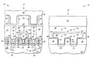
- FIG. 1is a fragmented, diagrammatic sectional view of semiconductor wafer fragments in process in accordance with an aspect of the invention.
- FIG. 2is a view of the FIG. 1 wafer fragments at a processing step subsequent to that shown by FIG. 1 .
- FIG. 3is a view of the FIG. 2 wafer fragments at a processing step subsequent to that shown by FIG. 2 .
- FIG. 4is a view of the FIG. 3 wafer fragments at a processing step subsequent to that shown by FIG. 3 .
- FIG. 5is a view of the FIG. 4 wafer fragments at a processing step subsequent to that shown by FIG. 4 .
- FIG. 6is a view of the FIG. 5 wafer fragments at a processing step subsequent to that shown by FIG. 5 .
- FIG. 7is a view of the FIG. 6 wafer fragments at a processing step subsequent to that shown by FIG. 6 .
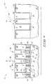
- FIG. 8is a diagrammatic top plan view of FIG. 7 .
- FIG. 9is a view of the FIG. 7 wafer fragments at a processing step subsequent to that shown by FIG. 7 .
- FIG. 10is a view of the FIG. 9 wafer fragments at a processing step subsequent to that shown by FIG. 9 .
- FIG. 11is a view of the FIG. 10 wafer fragments at a processing step subsequent to that shown by FIG. 10
- FIG. 12is a view of the FIG. 11 wafer fragments at a processing step subsequent to that shown by FIG. 11 .
- FIG. 13is a view of the FIG. 12 wafer fragments at a processing step subsequent to that shown by FIG. 12 .
- a semiconductor wafer fragment in processis shown generally with reference numeral 10 , and includes a semiconductive substrate 22 .
- semiconductor substrateor “semiconductive substrate” is defined to mean any construction comprising semiconductive material, including, but not limited to, bulk semiconductive materials such as a semiconductive wafer (either alone or in assemblies comprising other materials thereon), and semiconductive material layers (either alone or in assemblies comprising other materials).
- substraterefers to any supporting structure, including, but not limited to, the semiconductive substrates described above. Further in the context of this document, the term “layer” encompasses both the singular and the plural unless otherwise indicated.
- Substrate 22is shown in the form of bulk monocrystalline substrate, although semiconductor-on-insulator substrates and any other semiconductor substrate, whether existing or yet-to-be developed, are of course contemplated.
- the preferred embodiment substrate 10is depicted as having a memory array area 12 and a peripheral circuitry area 14 peripheral to memory array 12 .
- a plurality of spaced-apart word lines 19 , 21 , 23 and 25is formed over substrate 22 , and in part defines individual substrate locations 26 , 28 and 30 with which electrical communication is desired.
- Substrate locations 26 and 30on opposite sides of substrate location 28 , constitute locations with which electrical communication will be established with individual storage capacitors, and are referred to herein as capacitor nodes.
- Substrate location 28constitutes a location with which electrical communication will be established with a bit line, and is herein referred to as a bit node.
- the substrate locationscomprise diffusion regions 27 , 29 and 31 , respectively, which are received within substrate 22 .
- nodes 26 , 28 and 30might comprise other structures, for example elevated source/drains, plugs, etc., and include one or more conductive/semiconductive layers and whether existing or yet-to-be developed.
- Word lines 19 , 21 , 23 and 25 , and substrate locations 26 , 28 and 30are formed relative to an active area 32 which is isolated relative to other active areas by isolation regions 33 , and which can be formed through conventional or yet-to-be developed techniques, such as shallow trench isolation.
- Each exemplary preferred embodiment word lineis depicted as including a gate oxide layer 37 , a polysilicon layer 13 and a silicide or higher conductive layer 15 .
- An insulative cap 17is provided, as are insulative sidewall spacers 42 .
- Other word line constructions and or materialscan, of course, be utilized.
- word lines 21 and 23can be considered as comprising a first pair of word lines having a bit node 28 / 29 received therebetween, and word lines 23 and 25 can be considered as a second pair of word lines having a capacitor node 30 / 31 received therebetween.
- Peripheral circuitry area 14is depicted as having a first node 34 and a second node 35 . Such might constitute common or differing conductivity diffusion regions, as depicted, or might constitute any other conductive material node location where it is desired in one implementation to form some sort of local interconnecting line interconnecting a first node and a second node in the peripheral circuitry area.
- insulative material 36has been formed as part of substrate 10 .
- An exemplary materialis borophosphosilicate glass (BPSG), for example formed over an underlying layer (not specifically shown) of undoped silicon dioxide.
- BPSGborophosphosilicate glass
- Material 36 in the preferred embodimenthas been planarized, for example by CMP, although planarization is of course not required. Further if planarized, such might be conducted to produce an alternate construction, for example layer 36 could be planarized at least to the outer surface of caps 17 .
- a bit node contact opening 38 over bit node 28 , capacitor node contact openings 39 and 40 over capacitor nodes 26 and 30 , respectively, a first peripheral contact opening 41 over first node 34 , and a second peripheral contact opening 42 over second node 35have been formed within insulative material 36 .
- the depicted contact openingsare commonly formed, for example utilizing lithographic (i.e., photolithographic) patterning and etch steps which are common to the formation of the depicted contact openings.
- “commonly forming” or “commonly formed”, and “commonly replaced” or “commonly replacing”requires at least one or more processing steps which are common to the formation or removing of the stated material, structure or opening.
- the inventioncontemplates the fabrication of any and only a single one, or any subset, of the depicted contact openings as supported by the literal wording of the accompanying claims. However in the depicted embodiment, all openings are formed (preferably commonly) as shown in FIG. 2 , and regardless whether material 36 has been planarized, and if so to what degree or point.
- sacrificial plugging material 44is formed within bit node contact opening 38 , capacitor node contact openings 39 and 40 , first peripheral contact opening 41 and second peripheral contact opening 42 .
- the sacrificial plugging materialmight comprise insulative material, conductive material (including conductively doped semiconductive material) and/or semiconductive material regardless of whether conductively doped.
- sacrificial plugging material 44is shown as being in the form of a thin insulative liner 45 (i.e., silicon nitride or undoped silicon dioxide) having a doped or undoped planarized layer of polysilicon 46 formed thereover.
- diffusion regions 27 , 29 , 31 , 34 and 35comprise silicon to provide an etch stopping barrier between preferred polysilicon material 46 and such diffusion regions, as will be apparent from the continuing discussion.
- an interfacing etch stopping oxidemight be formed essentially only at node locations 26 , 28 , 30 , 34 and 35 by a thermal or plasma oxidation of the material of the respective diffusion regions.
- sacrificial plugging material 44is commonly formed with respect to openings 38 , 39 , 40 , 41 and 42 .
- sacrificial plugging material 44 and insulative material 36have been planarized back (i.e., by chemical-mechanical polishing) proximate to, more preferably at least to, an outer surface of insulative caps 17 .
- an insulating layer 48has been deposited.
- An exemplary materialis undoped silicon dioxide deposited by decomposition of tetraethylorthosilicate, with an exemplary thickness for layer 48 being 400 Angstroms.
- Contact openings/removal openings 50have been etched therethrough to sacrificial plugging material 44 within bit node contact opening 38 , first peripheral contact opening 41 and second peripheral contact opening 42 . Exemplary preferred techniques for doing so include lithographic patterning and etch.
- sacrificial plugging material 44has been removed from bit contact opening 38 , first peripheral contact opening 41 and second peripheral contact opening 42 while leaving sacrificial plugging 44 within capacitor node contact openings 39 and 40 .
- Preferred removing techniquesare by etching, with such etching removing the sacrificial plugging material from the bit node, first peripheral and second peripheral contact openings through removal openings 50 .
- an exemplary etching chemistryis aqueous tetramethylammonium hydroxide.
- insulative layer 45for example using an HF based chemistry for silicon dioxide, a fluorocarbon chemistry for silicon nitride) to clear layer 45 from over nodes 28 , 34 and 35 , as shown.
- conductive material 52that is in electrical connection with bit node 28 , first node 34 and second node 35 .
- conductive material 52is commonly replaced by deposition common to the substrate and the respective openings to result in the exemplary FIG. 6 construction.
- conductive material 52comprises a first layer 54 and a second layer 56 .
- layer 54might be formed to to provide a diffusion barrier function between substrate 22 and conductive layer 56 , and/or to provide an adhesion/glue layer function to facilitate adherence of layer 56 to the ultimate substrate.
- exemplary materials for layer 54include conductive metal suicides (whether chemical vapor deposited or formed by a salicide or other process), and conductive metal nitrides (whether stoichiometric, enriched in metal or other material), as well as any other conductive material.
- An exemplary material for layer 56is an elemental metal or an elemental alloy, for example tungsten.
- conductive material 52could comprise a single, or more than the illustrated two, layers and be any conductive material, including conductively doped semiconductive material.
- An insulative capping layer 58i.e., silicon nitride is formed over conductive material 52 .
- conductive material 52has been formed into a bit line 60 and a local interconnect line 62 .
- the top plan layout depicted by FIG. 8is merely an exemplary layout. Alternate layouts, whether existing or yet-to-be developed, could also of course be employed, for example as shown in our U.S. Pat. No. 6,458,649.
- An exemplary preferred method for forming the conductive material into the illustrated bit line and local interconnect lineincludes lithography (i.e., photolithography) and etch. However, any method of forming the respective materials into one or both of the illustrated lines is contemplated, whether existing or yet-to-be developed.
- bit line formingcould be by a damascene process.
- some suitable insulative materialcould be deposited over the FIG. 5 construction, with desired line-shaped troughs and contact openings etched therein. Conductive material could then be formed to overfill such troughs and openings and the conductive material planarized back to define the desired isolated conductive line outlines.
- the illustrated patterning to form lines 60 and 62comprises lithography and etch using at least some common lithographic and etching steps to the depicted layers, for example such that a single masking is conducted.
- anisotropically etched insulative sidewall spacers 64have been formed about the respective lines 60 and 62 .
- An exemplary preferred materialis silicon nitride.
- Subsequent processingwill preferably form a capacitor of a memory cell of the memory circuitry after having formed the bit line and local interconnect line. Such is shown, by way of example only, with respect to FIGS. 10-13 .
- another insulative layer 66has been deposited.
- An exemplary materialis BPSG. Openings 68 have been formed therethrough, and through insulative material 48 over sacrificial plugging material 44 received within remnant portions of capacitor node contact openings 39 and 40 .
- sacrificial plugging material 44has been removed from capacitor node contact openings 39 and 40 , for example as described above with respect to sacrificial material removal from openings 38 , 41 and 42 .
- conductive material 70has been deposited and planarized back to fill openings 68 .
- Suchmight, of course, include more than one conductive material.
- FIG. 13another insulative layer 72 has been deposited.
- Storage node container openings 74have been formed therein, and a storage node 76 , a capacitor dielectric layer 78 and a common outer capacitor plate 80 formed, as shown. Further and by way of example only, a contact opening (not shown) could be formed to local interconnect line 62 commensurate with the forming of container openings 74 .
- Suchprovides but one example of forming exemplary capacitors of respective memory cells of memory circuitry in electrical connection with capacitor nodes 26 and 30 , and whereby an elevationally outermost electrode (i.e., 80 ) of a capacitor is received everywhere elevationally outward of the illustrated bit line.
- an elevationally outermost electrodei.e. 80
- attributes of the inventionmight be practiced in the formation of memory circuitry not comprising buried bit line memory cells without departing from certain principles and aspects of the invention.
- the inventionmight provide an advantage over certain previous technology in the provision of low resistant contacts to the digit line node while enabling the commensurate fabrication of one, more or all local interconnect lines within the periphery between various metal, metal compound, n+ and p+ regions, with reduced masking steps where masking is utilized.
Landscapes
- Engineering & Computer Science (AREA)
- Manufacturing & Machinery (AREA)
- Physics & Mathematics (AREA)
- Condensed Matter Physics & Semiconductors (AREA)
- General Physics & Mathematics (AREA)
- Computer Hardware Design (AREA)
- Microelectronics & Electronic Packaging (AREA)
- Power Engineering (AREA)
- Internal Circuitry In Semiconductor Integrated Circuit Devices (AREA)
- Semiconductor Memories (AREA)
Abstract
Description
Claims (70)
Priority Applications (4)
| Application Number | Priority Date | Filing Date | Title |
|---|---|---|---|
| US10/615,287US6921692B2 (en) | 2003-07-07 | 2003-07-07 | Methods of forming memory circuitry |
| US11/135,534US7008843B2 (en) | 2003-07-07 | 2005-05-23 | Methods of forming memory circuitry |
| US11/292,028US7268384B2 (en) | 2003-07-07 | 2005-12-01 | Semiconductor substrate having first and second pairs of word lines |
| US11/515,648US7419865B2 (en) | 2003-07-07 | 2006-09-05 | Methods of forming memory circuitry |
Applications Claiming Priority (1)
| Application Number | Priority Date | Filing Date | Title |
|---|---|---|---|
| US10/615,287US6921692B2 (en) | 2003-07-07 | 2003-07-07 | Methods of forming memory circuitry |
Related Child Applications (1)
| Application Number | Title | Priority Date | Filing Date |
|---|---|---|---|
| US11/135,534ContinuationUS7008843B2 (en) | 2003-07-07 | 2005-05-23 | Methods of forming memory circuitry |
Publications (2)
| Publication Number | Publication Date |
|---|---|
| US20050009270A1 US20050009270A1 (en) | 2005-01-13 |
| US6921692B2true US6921692B2 (en) | 2005-07-26 |
Family
ID=33564530
Family Applications (4)
| Application Number | Title | Priority Date | Filing Date |
|---|---|---|---|
| US10/615,287Expired - Fee RelatedUS6921692B2 (en) | 2003-07-07 | 2003-07-07 | Methods of forming memory circuitry |
| US11/135,534Expired - Fee RelatedUS7008843B2 (en) | 2003-07-07 | 2005-05-23 | Methods of forming memory circuitry |
| US11/292,028Expired - LifetimeUS7268384B2 (en) | 2003-07-07 | 2005-12-01 | Semiconductor substrate having first and second pairs of word lines |
| US11/515,648Expired - LifetimeUS7419865B2 (en) | 2003-07-07 | 2006-09-05 | Methods of forming memory circuitry |
Family Applications After (3)
| Application Number | Title | Priority Date | Filing Date |
|---|---|---|---|
| US11/135,534Expired - Fee RelatedUS7008843B2 (en) | 2003-07-07 | 2005-05-23 | Methods of forming memory circuitry |
| US11/292,028Expired - LifetimeUS7268384B2 (en) | 2003-07-07 | 2005-12-01 | Semiconductor substrate having first and second pairs of word lines |
| US11/515,648Expired - LifetimeUS7419865B2 (en) | 2003-07-07 | 2006-09-05 | Methods of forming memory circuitry |
Country Status (1)
| Country | Link |
|---|---|
| US (4) | US6921692B2 (en) |
Families Citing this family (13)
| Publication number | Priority date | Publication date | Assignee | Title |
|---|---|---|---|---|
| US7838369B2 (en)* | 2005-08-29 | 2010-11-23 | National Semiconductor Corporation | Fabrication of semiconductor architecture having field-effect transistors especially suitable for analog applications |
| US20070202677A1 (en)* | 2006-02-27 | 2007-08-30 | Micron Technology, Inc. | Contact formation |
| US7713857B2 (en)* | 2008-03-20 | 2010-05-11 | Micron Technology, Inc. | Methods of forming an antifuse and a conductive interconnect, and methods of forming DRAM circuitry |
| KR101116361B1 (en)* | 2010-02-26 | 2012-03-09 | 주식회사 하이닉스반도체 | Method for fabricating semiconductor device |
| US8288795B2 (en) | 2010-03-02 | 2012-10-16 | Micron Technology, Inc. | Thyristor based memory cells, devices and systems including the same and methods for forming the same |
| US9608119B2 (en) | 2010-03-02 | 2017-03-28 | Micron Technology, Inc. | Semiconductor-metal-on-insulator structures, methods of forming such structures, and semiconductor devices including such structures |
| US9646869B2 (en) | 2010-03-02 | 2017-05-09 | Micron Technology, Inc. | Semiconductor devices including a diode structure over a conductive strap and methods of forming such semiconductor devices |
| US8507966B2 (en) | 2010-03-02 | 2013-08-13 | Micron Technology, Inc. | Semiconductor cells, arrays, devices and systems having a buried conductive line and methods for forming the same |
| US8598621B2 (en) | 2011-02-11 | 2013-12-03 | Micron Technology, Inc. | Memory cells, memory arrays, methods of forming memory cells, and methods of forming a shared doped semiconductor region of a vertically oriented thyristor and a vertically oriented access transistor |
| US8952418B2 (en) | 2011-03-01 | 2015-02-10 | Micron Technology, Inc. | Gated bipolar junction transistors |
| US8519431B2 (en) | 2011-03-08 | 2013-08-27 | Micron Technology, Inc. | Thyristors |
| US8772848B2 (en)* | 2011-07-26 | 2014-07-08 | Micron Technology, Inc. | Circuit structures, memory circuitry, and methods |
| IT202100020228A1 (en) | 2021-07-29 | 2023-01-29 | Chromaleont Srl | Method for the extraction of policosanols from industrial hemp and its mixture. |
Citations (25)
| Publication number | Priority date | Publication date | Assignee | Title |
|---|---|---|---|---|
| US5250457A (en) | 1992-02-19 | 1993-10-05 | Micron Technology, Inc. | Method of forming a buried bit line array of memory cells |
| US5387533A (en)* | 1992-08-25 | 1995-02-07 | Kim; Hong S. | Method of making dynamic random access memory |
| US5563089A (en) | 1994-07-20 | 1996-10-08 | Micron Technology, Inc. | Method of forming a bit line over capacitor array of memory cells and an array of bit line over capacitor array of memory cells |
| US5728617A (en)* | 1996-11-12 | 1998-03-17 | Vanguard International Semiconductor Corporation | Method for fabricating vertical walled stacked capacitors for dram cells |
| US5834349A (en)* | 1996-12-02 | 1998-11-10 | Vanguard International Semiconductor Corporation | Method for fabricating memory cells using chemical mechanical polishing technology |
| US5918122A (en) | 1997-02-11 | 1999-06-29 | Micron Technology, Inc. | Methods of forming integrated circuitry, DRAM cells and capacitors |
| US5981333A (en) | 1997-02-11 | 1999-11-09 | Micron Technology, Inc. | Methods of forming capacitors and DRAM arrays |
| US6015983A (en) | 1997-02-11 | 2000-01-18 | Micron Technology, Inc. | Bitline contact structures and DRAM array structures |
| US6037218A (en) | 1993-04-07 | 2000-03-14 | Micron Technology, Inc. | Semiconductor processing methods of forming stacked capacitors |
| US6060351A (en) | 1997-12-24 | 2000-05-09 | Micron Technology, Inc. | Process for forming capacitor over bit line memory cell |
| US6107189A (en) | 1997-03-05 | 2000-08-22 | Micron Technology, Inc. | Method of making a local interconnect using spacer-masked contact etch |
| US6177695B1 (en)* | 1998-12-21 | 2001-01-23 | Vanguard International Semiconductor Corporation | DRAM using oxide plug in bitline contacts during fabrication |
| US6228738B1 (en) | 1997-02-11 | 2001-05-08 | Micron Technology, Inc. | Methods of forming capacitors structures and DRAM cells |
| US6245631B1 (en) | 1999-12-06 | 2001-06-12 | Micron Technology, Inc. | Method of forming buried bit line memory circuitry and semiconductor processing method of forming a conductive line |
| US6284641B1 (en) | 1997-12-08 | 2001-09-04 | Micron Technology, Inc. | Method of forming a contact using a sacrificial spacer |
| US6312988B1 (en) | 1999-09-02 | 2001-11-06 | Micron Technology, Inc. | Methods of forming capacitors, methods of forming capacitor-over-bit line memory circuitry, and related integrated circuitry constructions |
| US6337274B1 (en) | 1999-12-06 | 2002-01-08 | Micron Technology, Inc. | Methods of forming buried bit line memory circuitry |
| US6359302B1 (en) | 1997-10-16 | 2002-03-19 | Micron Technology, Inc. | DRAM cells and integrated circuitry, and capacitor structures |
| US6376380B1 (en) | 2000-08-30 | 2002-04-23 | Micron Technology, Inc. | Method of forming memory circuitry and method of forming memory circuitry comprising a buried bit line array of memory cells |
| US6383868B1 (en) | 2000-08-31 | 2002-05-07 | Micron Technology, Inc. | Methods for forming contact and container structures, and integrated circuit devices therefrom |
| US6458649B1 (en) | 1999-07-22 | 2002-10-01 | Micron Technology, Inc. | Methods of forming capacitor-over-bit line memory cells |
| US6458859B2 (en) | 1999-12-10 | 2002-10-01 | Shin-Etsu Chemical Co., Ltd. | Semiconductive silicone rubber composition and silicone rubber roll |
| US6486060B2 (en) | 1998-09-03 | 2002-11-26 | Micron Technology, Inc. | Low resistance semiconductor process and structures |
| US6524907B2 (en) | 1999-09-20 | 2003-02-25 | Micron Technology, Inc. | Method of reducing electrical shorts from the bit line to the cell plate |
| US6589876B1 (en)* | 1999-07-22 | 2003-07-08 | Micron Technology, Inc. | Methods of forming conductive capacitor plugs, methods of forming capacitor contact openings, and methods of forming memory arrays |
Family Cites Families (7)
| Publication number | Priority date | Publication date | Assignee | Title |
|---|---|---|---|---|
| JP3941133B2 (en)* | 1996-07-18 | 2007-07-04 | 富士通株式会社 | Semiconductor device and manufacturing method thereof |
| US6010935A (en)* | 1997-08-21 | 2000-01-04 | Micron Technology, Inc. | Self aligned contacts |
| KR100282487B1 (en)* | 1998-10-19 | 2001-02-15 | 윤종용 | Cell Capacitor Using High-Dielectric Multilayer Film and Its Manufacturing Method |
| JP2000174225A (en)* | 1998-12-01 | 2000-06-23 | Hitachi Ltd | Semiconductor integrated circuit device and method of manufacturing the same |
| JP2001244436A (en)* | 2000-03-01 | 2001-09-07 | Hitachi Ltd | Semiconductor integrated circuit device and method of manufacturing the same |
| US6334692B1 (en)* | 2000-09-25 | 2002-01-01 | Yeong-Shyan Hsueh | Decorative member having vibration actuating light |
| KR20040049659A (en)* | 2002-12-06 | 2004-06-12 | 주식회사 하이닉스반도체 | A method for forming a capacitor of a semiconductor device |
- 2003
- 2003-07-07USUS10/615,287patent/US6921692B2/ennot_activeExpired - Fee Related
- 2005
- 2005-05-23USUS11/135,534patent/US7008843B2/ennot_activeExpired - Fee Related
- 2005-12-01USUS11/292,028patent/US7268384B2/ennot_activeExpired - Lifetime
- 2006
- 2006-09-05USUS11/515,648patent/US7419865B2/ennot_activeExpired - Lifetime
Patent Citations (42)
| Publication number | Priority date | Publication date | Assignee | Title |
|---|---|---|---|---|
| US5250457A (en) | 1992-02-19 | 1993-10-05 | Micron Technology, Inc. | Method of forming a buried bit line array of memory cells |
| US5387533A (en)* | 1992-08-25 | 1995-02-07 | Kim; Hong S. | Method of making dynamic random access memory |
| US5686747A (en) | 1993-02-12 | 1997-11-11 | Micron Technology, Inc. | Integrated circuits comprising interconnecting plugs |
| US5821140A (en) | 1993-02-12 | 1998-10-13 | Micron Technology, Inc. | Method of forming a bit line over capacitor array of memory cells and an array of bit line over capacitor array of memory cells |
| US6037218A (en) | 1993-04-07 | 2000-03-14 | Micron Technology, Inc. | Semiconductor processing methods of forming stacked capacitors |
| US6180450B1 (en) | 1993-04-07 | 2001-01-30 | Micron Technologies, Inc. | Semiconductor processing methods of forming stacked capacitors |
| US5563089A (en) | 1994-07-20 | 1996-10-08 | Micron Technology, Inc. | Method of forming a bit line over capacitor array of memory cells and an array of bit line over capacitor array of memory cells |
| US5728617A (en)* | 1996-11-12 | 1998-03-17 | Vanguard International Semiconductor Corporation | Method for fabricating vertical walled stacked capacitors for dram cells |
| US5834349A (en)* | 1996-12-02 | 1998-11-10 | Vanguard International Semiconductor Corporation | Method for fabricating memory cells using chemical mechanical polishing technology |
| US6238971B1 (en) | 1997-02-11 | 2001-05-29 | Micron Technology, Inc. | Capacitor structures, DRAM cell structures, and integrated circuitry, and methods of forming capacitor structures, integrated circuitry and DRAM cell structures |
| US6297525B1 (en) | 1997-02-11 | 2001-10-02 | Micron Technology , Inc. | Capacitor structures, DRAM cell structures, and integrated circuitry |
| US6500709B2 (en) | 1997-02-11 | 2002-12-31 | Micron Technology, Inc. | Capacitor structures, DRAM cell structures, and integrated circuitry, and methods of forming capacitor structures, integrated circuitry and DRAM cell structures |
| US6015983A (en) | 1997-02-11 | 2000-01-18 | Micron Technology, Inc. | Bitline contact structures and DRAM array structures |
| US6140172A (en) | 1997-02-11 | 2000-10-31 | Micron Technology, Inc. | Conductive electrical contacts, capacitors, DRAMs, and integrated circuitry, and methods of forming conductive electrical contacts, capacitors, DRAMs and integrated circuitry |
| US6376301B2 (en) | 1997-02-11 | 2002-04-23 | Micron Technology, Inc. | Methods of forming a capacitor and methods of forming a monolithic integrated circuit |
| US5981333A (en) | 1997-02-11 | 1999-11-09 | Micron Technology, Inc. | Methods of forming capacitors and DRAM arrays |
| US6214727B1 (en) | 1997-02-11 | 2001-04-10 | Micron Technology, Inc. | Conductive electrical contacts, capacitors, DRAMs, and integrated circuitry, and methods of forming conductive electrical contacts, capacitors, DRAMs, and integrated circuitry |
| US6228738B1 (en) | 1997-02-11 | 2001-05-08 | Micron Technology, Inc. | Methods of forming capacitors structures and DRAM cells |
| US6228710B1 (en) | 1997-02-11 | 2001-05-08 | Micron Technology, Inc. | Methods of forming capacitors and DRAM arrays |
| US6232176B1 (en) | 1997-02-11 | 2001-05-15 | Micron Technology, Inc. | Integrated circuitry, DRAM cells, capacitors, and methods of forming integrated circuitry, DRAM cells and capacitors |
| US5918122A (en) | 1997-02-11 | 1999-06-29 | Micron Technology, Inc. | Methods of forming integrated circuitry, DRAM cells and capacitors |
| US6329684B1 (en) | 1997-02-11 | 2001-12-11 | Micron Technology, Inc. | Capacitor structures, DRAM cells and integrated circuitry |
| US6323080B1 (en) | 1997-02-11 | 2001-11-27 | Micron Technology, Inc. | Conductive electrical contacts, capacitors, DRAMs, and integrated circuitry, and methods of forming conductive electrical contacts, capacitors, DRAMs, and integrated circuitry |
| US6407455B1 (en) | 1997-03-05 | 2002-06-18 | Micron Technology, Inc. | Local interconnect using spacer-masked contact etch |
| US6107189A (en) | 1997-03-05 | 2000-08-22 | Micron Technology, Inc. | Method of making a local interconnect using spacer-masked contact etch |
| US6359302B1 (en) | 1997-10-16 | 2002-03-19 | Micron Technology, Inc. | DRAM cells and integrated circuitry, and capacitor structures |
| US6284641B1 (en) | 1997-12-08 | 2001-09-04 | Micron Technology, Inc. | Method of forming a contact using a sacrificial spacer |
| US6329682B1 (en) | 1997-12-24 | 2001-12-11 | Micron Technology, Inc. | Capacitor over bit line memory cell and process |
| US6060351A (en) | 1997-12-24 | 2000-05-09 | Micron Technology, Inc. | Process for forming capacitor over bit line memory cell |
| US6486060B2 (en) | 1998-09-03 | 2002-11-26 | Micron Technology, Inc. | Low resistance semiconductor process and structures |
| US6177695B1 (en)* | 1998-12-21 | 2001-01-23 | Vanguard International Semiconductor Corporation | DRAM using oxide plug in bitline contacts during fabrication |
| US6458649B1 (en) | 1999-07-22 | 2002-10-01 | Micron Technology, Inc. | Methods of forming capacitor-over-bit line memory cells |
| US6589876B1 (en)* | 1999-07-22 | 2003-07-08 | Micron Technology, Inc. | Methods of forming conductive capacitor plugs, methods of forming capacitor contact openings, and methods of forming memory arrays |
| US6312988B1 (en) | 1999-09-02 | 2001-11-06 | Micron Technology, Inc. | Methods of forming capacitors, methods of forming capacitor-over-bit line memory circuitry, and related integrated circuitry constructions |
| US6524907B2 (en) | 1999-09-20 | 2003-02-25 | Micron Technology, Inc. | Method of reducing electrical shorts from the bit line to the cell plate |
| US6245631B1 (en) | 1999-12-06 | 2001-06-12 | Micron Technology, Inc. | Method of forming buried bit line memory circuitry and semiconductor processing method of forming a conductive line |
| US6368962B2 (en) | 1999-12-06 | 2002-04-09 | Micron Technology, Inc. | Semiconductor processing method of forming a conductive line, and buried bit line memory circuitry |
| US6337274B1 (en) | 1999-12-06 | 2002-01-08 | Micron Technology, Inc. | Methods of forming buried bit line memory circuitry |
| US6458859B2 (en) | 1999-12-10 | 2002-10-01 | Shin-Etsu Chemical Co., Ltd. | Semiconductive silicone rubber composition and silicone rubber roll |
| US6376380B1 (en) | 2000-08-30 | 2002-04-23 | Micron Technology, Inc. | Method of forming memory circuitry and method of forming memory circuitry comprising a buried bit line array of memory cells |
| US6383868B1 (en) | 2000-08-31 | 2002-05-07 | Micron Technology, Inc. | Methods for forming contact and container structures, and integrated circuit devices therefrom |
| US6617635B2 (en) | 2000-08-31 | 2003-09-09 | Micron Technology, Inc. | Integrated circuit devices having contact and container structures |
Also Published As
| Publication number | Publication date |
|---|---|
| US20050009270A1 (en) | 2005-01-13 |
| US20050207215A1 (en) | 2005-09-22 |
| US7008843B2 (en) | 2006-03-07 |
| US20070004132A1 (en) | 2007-01-04 |
| US7268384B2 (en) | 2007-09-11 |
| US7419865B2 (en) | 2008-09-02 |
| US20060082004A1 (en) | 2006-04-20 |
Similar Documents
| Publication | Publication Date | Title |
|---|---|---|
| US7419865B2 (en) | Methods of forming memory circuitry | |
| US7279419B2 (en) | Formation of self-aligned contact plugs | |
| US7439138B2 (en) | Method of forming integrated circuitry | |
| US6764893B2 (en) | Method for reducing a parasitic capacitance of a semiconductive memory cell using metal mask for sidewall formation | |
| US6080620A (en) | Method for fabricating interconnection and capacitors of a DRAM using a simple geometry active area, self-aligned etching, and polysilicon plugs | |
| US6399981B2 (en) | Integrated circuitry memory devices | |
| US20100227463A1 (en) | Methods of Forming Pad Structures and Related Methods of Manufacturing Recessed Channel Transistors that Include Such Pad Structures | |
| US20020024093A1 (en) | Semiconductor device with self-aligned contact structure employing dual spacers and method of manufacturing the same | |
| US7115491B2 (en) | Method for forming self-aligned contact in semiconductor device | |
| US6333233B1 (en) | Semiconductor device with self-aligned contact and its manufacture | |
| US7629218B2 (en) | Method of manufacturing a capacitor and method of manufacturing a semiconductor device using the same | |
| US7989335B2 (en) | Methods of forming insulation layer patterns and methods of manufacturing semiconductor devices including insulation layer patterns | |
| US7601586B2 (en) | Methods of forming buried bit line DRAM circuitry | |
| US7595521B2 (en) | Terraced film stack | |
| US6423627B1 (en) | Method for forming memory array and periphery contacts using a same mask | |
| US6376380B1 (en) | Method of forming memory circuitry and method of forming memory circuitry comprising a buried bit line array of memory cells | |
| US6680254B2 (en) | Method of fabricating bit line and bit line contact plug of a memory cell | |
| US6653230B2 (en) | Semiconductor device having concave electrode and convex electrode and method of manufacturing thereof | |
| US7109080B2 (en) | Method of forming capacitor over bitline contact | |
| KR20020002690A (en) | Manufacturing method for semiconductor device | |
| US20080044970A1 (en) | Memory structure and method for preparing the same |
Legal Events
| Date | Code | Title | Description |
|---|---|---|---|
| AS | Assignment | Owner name:MICRON TECHNOLOGY, INC., IDAHO Free format text:ASSIGNMENT OF ASSIGNORS INTEREST;ASSIGNORS:PAREKH, KUNAL R.;BURGESS, BYRON N.;REEL/FRAME:014279/0410 Effective date:20030630 | |
| FEPP | Fee payment procedure | Free format text:PAYOR NUMBER ASSIGNED (ORIGINAL EVENT CODE: ASPN); ENTITY STATUS OF PATENT OWNER: LARGE ENTITY | |
| CC | Certificate of correction | ||
| FPAY | Fee payment | Year of fee payment:4 | |
| FPAY | Fee payment | Year of fee payment:8 | |
| AS | Assignment | Owner name:U.S. BANK NATIONAL ASSOCIATION, AS COLLATERAL AGENT, CALIFORNIA Free format text:SECURITY INTEREST;ASSIGNOR:MICRON TECHNOLOGY, INC.;REEL/FRAME:038669/0001 Effective date:20160426 Owner name:U.S. BANK NATIONAL ASSOCIATION, AS COLLATERAL AGEN Free format text:SECURITY INTEREST;ASSIGNOR:MICRON TECHNOLOGY, INC.;REEL/FRAME:038669/0001 Effective date:20160426 | |
| AS | Assignment | Owner name:MORGAN STANLEY SENIOR FUNDING, INC., AS COLLATERAL AGENT, MARYLAND Free format text:PATENT SECURITY AGREEMENT;ASSIGNOR:MICRON TECHNOLOGY, INC.;REEL/FRAME:038954/0001 Effective date:20160426 Owner name:MORGAN STANLEY SENIOR FUNDING, INC., AS COLLATERAL Free format text:PATENT SECURITY AGREEMENT;ASSIGNOR:MICRON TECHNOLOGY, INC.;REEL/FRAME:038954/0001 Effective date:20160426 | |
| REMI | Maintenance fee reminder mailed | ||
| AS | Assignment | Owner name:U.S. BANK NATIONAL ASSOCIATION, AS COLLATERAL AGENT, CALIFORNIA Free format text:CORRECTIVE ASSIGNMENT TO CORRECT THE REPLACE ERRONEOUSLY FILED PATENT #7358718 WITH THE CORRECT PATENT #7358178 PREVIOUSLY RECORDED ON REEL 038669 FRAME 0001. ASSIGNOR(S) HEREBY CONFIRMS THE SECURITY INTEREST;ASSIGNOR:MICRON TECHNOLOGY, INC.;REEL/FRAME:043079/0001 Effective date:20160426 Owner name:U.S. BANK NATIONAL ASSOCIATION, AS COLLATERAL AGEN Free format text:CORRECTIVE ASSIGNMENT TO CORRECT THE REPLACE ERRONEOUSLY FILED PATENT #7358718 WITH THE CORRECT PATENT #7358178 PREVIOUSLY RECORDED ON REEL 038669 FRAME 0001. ASSIGNOR(S) HEREBY CONFIRMS THE SECURITY INTEREST;ASSIGNOR:MICRON TECHNOLOGY, INC.;REEL/FRAME:043079/0001 Effective date:20160426 | |
| LAPS | Lapse for failure to pay maintenance fees | Free format text:PATENT EXPIRED FOR FAILURE TO PAY MAINTENANCE FEES (ORIGINAL EVENT CODE: EXP.) | |
| STCH | Information on status: patent discontinuation | Free format text:PATENT EXPIRED DUE TO NONPAYMENT OF MAINTENANCE FEES UNDER 37 CFR 1.362 | |
| FP | Lapsed due to failure to pay maintenance fee | Effective date:20170726 | |
| AS | Assignment | Owner name:MICRON TECHNOLOGY, INC., IDAHO Free format text:RELEASE BY SECURED PARTY;ASSIGNOR:U.S. BANK NATIONAL ASSOCIATION, AS COLLATERAL AGENT;REEL/FRAME:047243/0001 Effective date:20180629 | |
| AS | Assignment | Owner name:MICRON TECHNOLOGY, INC., IDAHO Free format text:RELEASE BY SECURED PARTY;ASSIGNOR:MORGAN STANLEY SENIOR FUNDING, INC., AS COLLATERAL AGENT;REEL/FRAME:050937/0001 Effective date:20190731 |