US6920523B2 - Bank address mapping according to bank retention time in dynamic random access memories - Google Patents
Bank address mapping according to bank retention time in dynamic random access memoriesDownload PDFInfo
- Publication number
- US6920523B2 US6920523B2US10/265,964US26596402AUS6920523B2US 6920523 B2US6920523 B2US 6920523B2US 26596402 AUS26596402 AUS 26596402AUS 6920523 B2US6920523 B2US 6920523B2
- Authority
- US
- United States
- Prior art keywords
- memory
- bank
- refresh
- memory banks
- banks
- Prior art date
- Legal status (The legal status is an assumption and is not a legal conclusion. Google has not performed a legal analysis and makes no representation as to the accuracy of the status listed.)
- Expired - Fee Related, expires
Links
Images


Classifications
- G—PHYSICS
- G06—COMPUTING OR CALCULATING; COUNTING
- G06F—ELECTRIC DIGITAL DATA PROCESSING
- G06F1/00—Details not covered by groups G06F3/00 - G06F13/00 and G06F21/00
- G06F1/26—Power supply means, e.g. regulation thereof
- G06F1/32—Means for saving power
- G06F1/3203—Power management, i.e. event-based initiation of a power-saving mode
- G06F1/3234—Power saving characterised by the action undertaken
- G06F1/325—Power saving in peripheral device
- G06F1/3275—Power saving in memory, e.g. RAM, cache
- G—PHYSICS
- G06—COMPUTING OR CALCULATING; COUNTING
- G06F—ELECTRIC DIGITAL DATA PROCESSING
- G06F12/00—Accessing, addressing or allocating within memory systems or architectures
- G06F12/02—Addressing or allocation; Relocation
- G06F12/06—Addressing a physical block of locations, e.g. base addressing, module addressing, memory dedication
- G—PHYSICS
- G06—COMPUTING OR CALCULATING; COUNTING
- G06F—ELECTRIC DIGITAL DATA PROCESSING
- G06F12/00—Accessing, addressing or allocating within memory systems or architectures
- G06F12/02—Addressing or allocation; Relocation
- G06F12/08—Addressing or allocation; Relocation in hierarchically structured memory systems, e.g. virtual memory systems
- G06F12/0802—Addressing of a memory level in which the access to the desired data or data block requires associative addressing means, e.g. caches
- G06F12/0844—Multiple simultaneous or quasi-simultaneous cache accessing
- G06F12/0846—Cache with multiple tag or data arrays being simultaneously accessible
- G—PHYSICS
- G06—COMPUTING OR CALCULATING; COUNTING
- G06F—ELECTRIC DIGITAL DATA PROCESSING
- G06F12/00—Accessing, addressing or allocating within memory systems or architectures
- G06F12/02—Addressing or allocation; Relocation
- G06F12/08—Addressing or allocation; Relocation in hierarchically structured memory systems, e.g. virtual memory systems
- G06F12/0802—Addressing of a memory level in which the access to the desired data or data block requires associative addressing means, e.g. caches
- G06F12/0893—Caches characterised by their organisation or structure
- G—PHYSICS
- G06—COMPUTING OR CALCULATING; COUNTING
- G06F—ELECTRIC DIGITAL DATA PROCESSING
- G06F2212/00—Indexing scheme relating to accessing, addressing or allocation within memory systems or architectures
- G06F2212/10—Providing a specific technical effect
- G06F2212/1028—Power efficiency
- Y—GENERAL TAGGING OF NEW TECHNOLOGICAL DEVELOPMENTS; GENERAL TAGGING OF CROSS-SECTIONAL TECHNOLOGIES SPANNING OVER SEVERAL SECTIONS OF THE IPC; TECHNICAL SUBJECTS COVERED BY FORMER USPC CROSS-REFERENCE ART COLLECTIONS [XRACs] AND DIGESTS
- Y02—TECHNOLOGIES OR APPLICATIONS FOR MITIGATION OR ADAPTATION AGAINST CLIMATE CHANGE
- Y02D—CLIMATE CHANGE MITIGATION TECHNOLOGIES IN INFORMATION AND COMMUNICATION TECHNOLOGIES [ICT], I.E. INFORMATION AND COMMUNICATION TECHNOLOGIES AIMING AT THE REDUCTION OF THEIR OWN ENERGY USE
- Y02D10/00—Energy efficient computing, e.g. low power processors, power management or thermal management
Definitions
- the present disclosurerelates to dynamic random access memories (“DRAMs”), and more particularly, to a method and apparatus for mapping memory bank addresses relative to memory bank retention times in DRAMs.
- DRAMsdynamic random access memories
- a memory hierarchysupports a central processing unit (“CPU”) with data storage capabilities.
- CPUcentral processing unit
- RAMprimary random access memory
- DRAMdynamic random access memory
- SRAMstatic random access memory
- DRAMsSince data stored in DRAMs is destroyed after being idle for a period of time, DRAMs require refresh cycles to restore their data. Memory cells in DRAMs must be periodically refreshed within a certain period of time. This period of time is called the “retention time”. Depending on such factors as the chip technology and the chip temperature, the retention time may range from a few milliseconds to hundreds of milliseconds.
- Each DRAM memorymay be organized into arrays or banks.
- Data refreshis typically accomplished by accessing each row in each memory bank, one row in each bank at a time.
- data stored in memory cells of the banksare read to sense-amplifiers, and immediately written back to the memory cells.
- a capacitor corresponding to each memory cellis thus recharged to its initial value.
- Such refresh cycles in DRAMsconsume power, which may be at a premium in battery-powered mobile computing systems, for example.
- the systemincludes a data memory having a plurality of memory banks. Each bank is a collection of rows, which means that the mapping is not necessarily restricted in a bank, but can cover part of a bank.
- a map memoryis in signal communication with the data memory for translating an internal address of each of the plurality of memory banks into a corresponding external address, a map comparator in signal communication with the map memory for selectively enabling a memory bank in accordance with its external address, a refresh address generator in signal communication with the map comparator for selectively refreshing the enabled memory bank in accordance with its external address, and a refresh counter in signal communication with the refresh address generator for signaling a refresh in accordance with the maximum required refresh time of the enabled memory bank.
- the corresponding method for mapping memory bank addresses relative to memory bank retention times in DRAMsincludes determining the maximum required refresh period for each of the memory banks, respectively, prioritizing the memory banks in accordance with their respective refresh periods, utilizing the memory banks in order of their respective prioritizations, selectively disabling at least one of the memory banks in reverse-order of their respective prioritizations, and refreshing only the remaining non-disabled memory banks.
- the present disclosureteaches a system and method for mapping memory bank addresses relative to memory bank retention times in DRAMs, in accordance with the following exemplary figures, in which:
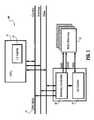
- FIG. 1shows a block diagram of a computing system with memory where exemplary embodiments of the present disclosure are applied
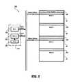
- FIG. 2shows a block diagram illustrating a DRAM memory of FIG. 1 ;
- FIG. 3shows a block diagram illustrating several memory banks of the DRAM memory of FIG. 2 ;
- FIG. 4shows a flow diagram for mapping memory bank addresses relative to memory bank retention times in DRAMs according to an exemplary embodiment of the present disclosure.
- a system and methodare provided for mapping memory bank addresses relative to memory bank retention times in dynamic random access memories (“DRAMs”).
- DRAMsdynamic random access memories
- Battery-powered mobile computing systemstypically have a power-down mode to reduce power consumption by the display and/or other peripheral devices during periods of low usage.
- the present disclosurepresents a system and method to further reduce the power consumption of a DRAM device.
- a feature referred to as a “partial array self-refresh”has been introduced in mobile DRAMs. This feature allows the DRAM chip to refresh only selected banks during a power-down mode. Either one bank, two banks or all banks may be activated and refreshed during the power-down mode. Non-activated banks are not refreshed, and are permitted to lose their data.
- a bank re-mapping relative to the retention timesis presented in this disclosure.
- the bank with the longest retention timewill be automatically selected first.
- the total refresh energyis already reduced by eliminating the need to refresh one or more banks.
- the total refresh energyis further reduced since the higher prioritized remapped banks have longer refresh periods than those banks given the lower re-mapping prioritizations.
- BA intf (BA ext , t retention )
- BA intf (BA ext , t retention )
- BA intf (BA ext , t retention )
- the internal bank addressis selected according to an ascending or descending refresh period by a multiplexer following determination of the refresh period for each bank.
- BA int ⁇ 0>may be set to correspond to the bank with the longest retention time while BA int ⁇ 3> may be set to correspond to the bank with the shortest retention time.
- selection of the refresh periods and bank address mappingscan be programmed via fuse options and/or programmable elements, such as, for example, EPROMs and flash memories.
- DRAMdynamic random access memory
- the computing system 100includes a central processing unit (“CPU”) 11 with an “on-chip” cache memory (“L1 Cache”) 13 , a main memory 15 , a CPU bus 17 , a memory controller 18 for controlling data traffic on the CPU bus 17 , and a second level cache memory (“L2 Cache”) 19 .
- CPUcentral processing unit
- L1 Cachecache memory
- main memory 15main memory
- main memory 15main memory
- main memory 15main memory 15
- main memory 15main memory
- main memory 15main memory 15
- CPU bus 17main memory
- memory controller 18for controlling data traffic on the CPU bus 17
- L2 Cachesecond level cache memory
- the first level cache memory 13is integrated on the same chip with the CPU 11 .
- the first level cache memory 13is faster because it is integrated with the CPU 11 with a higher bandwidth and shorter wire length and therefore avoids any delay associated with transmitting and/or receiving signals to and/or from an external chip.
- the second level cache memory 19is located on a different chip than the CPU, and has a larger capacity than the first level cache memory 13 but smaller than a main memory 15 .
- the second level cache memory 19is implemented in DRAM.
- the cache memories 13 and 19serve as buffers between the CPU 11 and the main memory 15 .
- data wordsare stored in the cache memory and grouped into small pages called ‘cache blocks’ or ‘cache lines’.
- the contents of the cache memoryare a copy of a set of main memory blocks.
- Each cache lineis marked with a “map address”. Thus, each cache line knows what part of the main memory the cache line belongs to.
- Map addresseswhich may be non-contiguous, that are assigned to the corresponding cache lines are stored in a special memory, called a “map memory” or “directory”.
- the first level cache memory 13when an address is requested by the CPU 11 to access certain data, if the requested address is not found in the L1 cache memory 13 , it is determined that the data corresponding to the requested address is not present in the cache memory 13 , which is referred to as “miss”.
- missWhen a miss occurs in the first level L1 cache memory 13 , the requested address is sent to a lower level memory, such as, for example, the second level L2 cache memory 19 .
- the data access process in the second level cache memoryis described in detail below. If a “miss” occurs in the second level cache memory 19 , the requested address is sent to the main memory 15 .
- the computing systempreferably employs SRAM for the first level cache memory 13 and DRAM for the second level cache memory 19 , no data refresh process is required for the first level cache memory 13 .
- SRAMstatic random access memory
- DRAMdynamic random access memory
- no data refresh processis required for the first level cache memory 13 .
- a method of refreshing data according to the present inventionis described with respect to the second level cache memory 19 .
- the present inventionis equally applicable to any DRAM memory, such as, for example, any DRAM memory used anywhere in a hierarchical memory system.
- a DRAMis generally indicated by the reference numeral 200 .
- the second level L2 cache memory 19includes a data memory 191 and a map memory 192 .
- the data memory 191stores data with a higher probability of being selected by the CPU 11 of FIG. 1
- the map memory 192stores map addresses, each addressing a corresponding cache line of the data stored in the data memory 191 .
- a requested address made by the CPUis loaded on the CPU bus 17 of FIG. 1 to be transferred to the second level L2 cache memory 19 .
- the memory controller 18 of FIG. 1receives the requested address from the CPU bus and sends the requested address to a map comparator 193 included in a map refresh controller 194 .
- the map comparator 193compares the requested address with map addresses provided from the map memory 192 of the cache memory 19 . If the requested address is found among the map addresses in the map memory, which is called a “hit”, a cache line corresponding to the requested address or the selected map address is accessed in the data memory 191 by the CPU . If the requested address is not found in the map addresses in the map memory, a “miss” occurs and the requested address is sent to the main memory 15 of FIG. 1 to find the data corresponding to the requested address in the main memory.
- the map refresh controller 194is provided for refreshing data stored in the data memory 191 of the DRAM cache memory 19 .
- the map refresh controller 194is used to trace memory addresses requiring a data refresh process.
- the map refresh controller 194also includes a refresh address generator 320 and a refresh counter 322 .
- the reference numeral 300generally indicates a DRAM data memory with word line addresses applied to the memory contents.
- the DRAM data memory 300has multiple banks, 41 , 42 , 43 and 44 , respectively, each bank having a corresponding sense amplifier, 401 , 402 , 403 and 404 , respectively.
- Each bankis a collection of rows.
- the mappingis not necessarily restricted to an entire bank, but may cover a portion of a bank, such as, for example, one or more rows.
- Data stored in each of the banksmay be accessed by a corresponding word line address. Assuming that a word line on which a read/write operation requested by the CPU 11 of FIG. 1 is to be performed is located in a first bank 41 , the access address corresponding to the word line is provided to the first bank 41 . In this exemplary embodiment, no refresh operation is allowed during normal access.
- the refresh address generator 320In a power-up mode of operation, the refresh address generator 320 generates refresh addresses for the first through fourth banks 41 - 44 , respectively.
- the information needed for each bank during refreshis the corresponding refresh rate for that bank.
- each word line data in each of the non-disabled banksis accessed with each of the refresh addresses when the fourth bank is disabled or otherwise powered-down.
- the fourth bank 44is determined to have a relatively shorter refresh time requirement.
- each bankis identified, for example, by the first two digits of an address to access a word line in the bank.
- the first two digits of a word line addressmay be ‘00’, ‘01’, ‘10’, or ‘11’, which designates the first 41 , second 42 , third 43 , or fourth bank 44 , respectively.
- a refresh address generator 320preferably includes a refresh counter 322 , which provides refresh timing and addresses of word lines for each bank in which a refresh operation is to be performed.
- the refresh counter 322is, for example, tracking the word line addresses for each bank to be refreshed. When one word line data is refreshed, the refresh counter 322 generates the next address of the bank for refresh. When all the word lines in the activated bank are refreshed, the refresh counter 322 will be reset to zero and starts to refresh the first word line again in the next refresh cycle. It shall be understood that in alternate embodiments where the disabled portions of memory do not comprise entire banks, the refresh counter may be initialized to one or more non-zero values.
- nis four in this exemplary embodiment, and where each such bank stores data accessed by word line addresses, disabling of a bank during a power-down mode is performed with respect to a bank and data refresh operations can be performed with respect to the remaining n minus one banks simultaneously. In other words, no extra power is required to perform the data refresh operation with respect to the disabled banks in the cache memory. Therefore, power is conserved for data refresh operations in the DRAM cache memory due to fewer banks being refreshed at longer refresh intervals, where the disabled banks are chosen in order of their relatively shorter refresh intervals. It shall be understood that alternate embodiments may disable one or more portions of a bank or banks without disabling the entire bank or banks, especially in cases where the disabled portion or portions of the bank or banks are determined to require a shorter refresh period than the enabled portions.
- a start block 410passes control to a function block 412 , which determines the maximum required refresh period for each of the memory banks, respectively.
- the function block 412passes control to a function block 414 , which prioritizes the memory banks in accordance with their respective refresh periods.
- the function block 414passes control to a function block 416 , which utilizes the memory banks in order of their respective prioritizations.
- the function block 416passes control to a function block 418 , which selectively disables at least one of the memory banks in reverse-order of their respective prioritizations.
- the function block 418passes control to a function block 420 , which refreshes only the remaining non-disabled memory banks, and passes control to an end block 428 .
- the exemplary method for mapping memory bank addresses relative to memory bank retention times in DRAMsincludes determining the maximum required refresh period for each of the memory banks, respectively, prioritizing the memory banks in accordance with their respective refresh periods, utilizing the memory banks in order of their respective prioritizations, selectively disabling at least one of the memory banks in reverse-order of their respective prioritizations, and refreshing only the remaining non-disabled memory banks.
- Some preferred and alternate embodiment methodscan determine the respective maximum refresh period for each of said memory banks by actual testing of the memory cell retention times for each bank. These embodiments may test the memory cell retention times for each bank, in turn, with automatic self-testing by the DRAM. The automatic self-testing of the memory cell retention times by the DRAM may be performed periodically, or it may be performed in response to a temperature change of the DRAM. Determination of the maximum required refresh period for each of the memory banks may also include measuring the temperature of the DRAM and adjusting the tested memory cell retention times for each bank in accordance with a predicted offset for temperature.
- Some preferred and alternate embodiment methodsalso include re-mapping the bank addresses of the memory banks in accordance with their respective prioritizations.
- the refreshing of only the remaining non-disabled memory banksmay be performed separately for each non-disabled memory bank in accordance with its respective refresh period, or it may be performed simultaneously for each non-disabled memory bank in accordance with the minimum of their respective maximum required refresh periods.
Landscapes
- Engineering & Computer Science (AREA)
- Theoretical Computer Science (AREA)
- Physics & Mathematics (AREA)
- General Engineering & Computer Science (AREA)
- General Physics & Mathematics (AREA)
- Dram (AREA)
Abstract
Description
Claims (18)
Priority Applications (2)
| Application Number | Priority Date | Filing Date | Title |
|---|---|---|---|
| US10/265,964US6920523B2 (en) | 2002-10-07 | 2002-10-07 | Bank address mapping according to bank retention time in dynamic random access memories |
| DE10345383ADE10345383B4 (en) | 2002-10-07 | 2003-09-30 | Bank address mapping according to a bank holding time in dynamic random access memories |
Applications Claiming Priority (1)
| Application Number | Priority Date | Filing Date | Title |
|---|---|---|---|
| US10/265,964US6920523B2 (en) | 2002-10-07 | 2002-10-07 | Bank address mapping according to bank retention time in dynamic random access memories |
Publications (2)
| Publication Number | Publication Date |
|---|---|
| US20040068604A1 US20040068604A1 (en) | 2004-04-08 |
| US6920523B2true US6920523B2 (en) | 2005-07-19 |
Family
ID=32030336
Family Applications (1)
| Application Number | Title | Priority Date | Filing Date |
|---|---|---|---|
| US10/265,964Expired - Fee RelatedUS6920523B2 (en) | 2002-10-07 | 2002-10-07 | Bank address mapping according to bank retention time in dynamic random access memories |
Country Status (2)
| Country | Link |
|---|---|
| US (1) | US6920523B2 (en) |
| DE (1) | DE10345383B4 (en) |
Cited By (21)
| Publication number | Priority date | Publication date | Assignee | Title |
|---|---|---|---|---|
| US20060250874A1 (en)* | 2005-01-17 | 2006-11-09 | Jong-Won Lee | Refresh control circuit and method thereof and bank address signal change circuit and methods thereof |
| US20070033339A1 (en)* | 2005-08-04 | 2007-02-08 | Best Scott C | Memory with refresh cycle donation to accommodate low-retention storage rows |
| US20070033338A1 (en)* | 2005-08-04 | 2007-02-08 | Tsern Ely K | Memory with address-differentiated refresh rate to accommodate low-retention storage rows |
| US20070030746A1 (en)* | 2005-08-04 | 2007-02-08 | Best Scott C | Memory device testing to support address-differentiated refresh rates |
| US20080270683A1 (en)* | 2007-04-25 | 2008-10-30 | International Business Machines Corporation | Systems and methods for a dram concurrent refresh engine with processor interface |
| US20100054070A1 (en)* | 2004-07-15 | 2010-03-04 | Micron Technology, Inc. | Method and system for controlling refresh to avoid memory cell data losses |
| US20100080075A1 (en)* | 2008-09-29 | 2010-04-01 | Qimonda North America Corp. | Memory Device Refresh Method and Apparatus |
| US7836374B2 (en)* | 2004-05-06 | 2010-11-16 | Micron Technology, Inc. | Memory controller method and system compensating for memory cell data losses |
| US20110007592A1 (en)* | 2009-07-10 | 2011-01-13 | Nec Electronics Corporation | Semiconductor storage device and refresh control method thereof |
| US7894289B2 (en) | 2006-10-11 | 2011-02-22 | Micron Technology, Inc. | Memory system and method using partial ECC to achieve low power refresh and fast access to data |
| US7900120B2 (en) | 2006-10-18 | 2011-03-01 | Micron Technology, Inc. | Memory system and method using ECC with flag bit to identify modified data |
| US20110296095A1 (en)* | 2010-05-25 | 2011-12-01 | Mediatek Inc. | Data movement engine and memory control methods thereof |
| US8078791B1 (en)* | 2007-04-16 | 2011-12-13 | Juniper Networks, Inc. | Ordering refresh requests to memory |
| US8799553B2 (en) | 2010-04-13 | 2014-08-05 | Apple Inc. | Memory controller mapping on-the-fly |
| US8848471B2 (en) | 2012-08-08 | 2014-09-30 | International Business Machines Corporation | Method for optimizing refresh rate for DRAM |
| US8887014B2 (en) | 2012-12-11 | 2014-11-11 | International Business Machines Corporation | Managing errors in a DRAM by weak cell encoding |
| US8898544B2 (en) | 2012-12-11 | 2014-11-25 | International Business Machines Corporation | DRAM error detection, evaluation, and correction |
| US9058896B2 (en) | 2012-08-29 | 2015-06-16 | International Business Machines Corporation | DRAM refresh |
| US9990293B2 (en) | 2014-08-12 | 2018-06-05 | Empire Technology Development Llc | Energy-efficient dynamic dram cache sizing via selective refresh of a cache in a dram |
| US10176107B2 (en) | 2014-03-29 | 2019-01-08 | Empire Technology Development Llc | Methods and systems for dynamic DRAM cache sizing |
| US11133077B2 (en) | 2020-02-20 | 2021-09-28 | Yangtze Memory Technologies Co., Ltd. | Method of programming multi-plane memory device for accelerating program speed and reducing program disturbance |
Families Citing this family (22)
| Publication number | Priority date | Publication date | Assignee | Title |
|---|---|---|---|---|
| US8065277B1 (en) | 2003-01-17 | 2011-11-22 | Daniel John Gardner | System and method for a data extraction and backup database |
| US8943024B1 (en) | 2003-01-17 | 2015-01-27 | Daniel John Gardner | System and method for data de-duplication |
| US8630984B1 (en) | 2003-01-17 | 2014-01-14 | Renew Data Corp. | System and method for data extraction from email files |
| US8375008B1 (en) | 2003-01-17 | 2013-02-12 | Robert Gomes | Method and system for enterprise-wide retention of digital or electronic data |
| US20050108460A1 (en)* | 2003-11-14 | 2005-05-19 | Intel Corporation | Partial bank DRAM refresh |
| US7392339B2 (en)* | 2003-12-10 | 2008-06-24 | Intel Corporation | Partial bank DRAM precharge |
| US8069151B1 (en) | 2004-12-08 | 2011-11-29 | Chris Crafford | System and method for detecting incongruous or incorrect media in a data recovery process |
| US8527468B1 (en)* | 2005-02-08 | 2013-09-03 | Renew Data Corp. | System and method for management of retention periods for content in a computing system |
| US20080189273A1 (en)* | 2006-06-07 | 2008-08-07 | Digital Mandate, Llc | System and method for utilizing advanced search and highlighting techniques for isolating subsets of relevant content data |
| US8150827B2 (en) | 2006-06-07 | 2012-04-03 | Renew Data Corp. | Methods for enhancing efficiency and cost effectiveness of first pass review of documents |
| US8438365B2 (en)* | 2006-10-06 | 2013-05-07 | Calos Fund Limited Liability Company | Efficient data loading in a data-parallel processor |
| US7613060B2 (en) | 2007-05-21 | 2009-11-03 | Micron Technology, Inc. | Methods, circuits, and systems to select memory regions |
| US8615490B1 (en) | 2008-01-31 | 2013-12-24 | Renew Data Corp. | Method and system for restoring information from backup storage media |
| WO2011072172A1 (en)* | 2009-12-09 | 2011-06-16 | Renew Data Corp. | System and method for quickly determining a subset of irrelevant data from large data content |
| WO2011075610A1 (en) | 2009-12-16 | 2011-06-23 | Renew Data Corp. | System and method for creating a de-duplicated data set |
| KR20130078455A (en) | 2011-12-30 | 2013-07-10 | 삼성전자주식회사 | Semiconductor memory device storing memory characteristic information, memory module and memory system having the same and operating method thereof |
| US9218285B2 (en)* | 2012-11-26 | 2015-12-22 | Arm Limited | Variable mapping of memory accesses to regions within a memory |
| US9396109B2 (en)* | 2013-12-27 | 2016-07-19 | Qualcomm Incorporated | Method and apparatus for DRAM spatial coalescing within a single channel |
| US20150206574A1 (en)* | 2014-01-22 | 2015-07-23 | Advanced Micro Devices, Inc. | Relocating infrequently-accessed dynamic random access memory (dram) data to non-volatile storage |
| KR20160023274A (en)* | 2014-08-22 | 2016-03-03 | 에스케이하이닉스 주식회사 | Memory device and memory including the same |
| WO2017151567A1 (en)* | 2016-03-01 | 2017-09-08 | University Of Rochester | Content aware refresh |
| US10332582B2 (en) | 2017-08-02 | 2019-06-25 | Qualcomm Incorporated | Partial refresh technique to save memory refresh power |
Citations (3)
| Publication number | Priority date | Publication date | Assignee | Title |
|---|---|---|---|---|
| US6446159B2 (en)* | 1997-06-12 | 2002-09-03 | Matsushita Electric Industrial Co., Ltd. | Semiconductor circuit and method of controlling the same |
| US20030028711A1 (en)* | 2001-07-30 | 2003-02-06 | Woo Steven C. | Monitoring in-use memory areas for power conservation |
| US6557072B2 (en)* | 2001-05-10 | 2003-04-29 | Palm, Inc. | Predictive temperature compensation for memory devices systems and method |
Family Cites Families (2)
| Publication number | Priority date | Publication date | Assignee | Title |
|---|---|---|---|---|
| JP3714489B2 (en)* | 1995-03-03 | 2005-11-09 | 株式会社日立製作所 | Dynamic RAM and memory module |
| TW324101B (en)* | 1995-12-21 | 1998-01-01 | Hitachi Ltd | Semiconductor integrated circuit and its working method |
- 2002
- 2002-10-07USUS10/265,964patent/US6920523B2/ennot_activeExpired - Fee Related
- 2003
- 2003-09-30DEDE10345383Apatent/DE10345383B4/ennot_activeExpired - Fee Related
Patent Citations (3)
| Publication number | Priority date | Publication date | Assignee | Title |
|---|---|---|---|---|
| US6446159B2 (en)* | 1997-06-12 | 2002-09-03 | Matsushita Electric Industrial Co., Ltd. | Semiconductor circuit and method of controlling the same |
| US6557072B2 (en)* | 2001-05-10 | 2003-04-29 | Palm, Inc. | Predictive temperature compensation for memory devices systems and method |
| US20030028711A1 (en)* | 2001-07-30 | 2003-02-06 | Woo Steven C. | Monitoring in-use memory areas for power conservation |
Cited By (51)
| Publication number | Priority date | Publication date | Assignee | Title |
|---|---|---|---|---|
| US9064600B2 (en) | 2004-05-06 | 2015-06-23 | Micron Technology, Inc. | Memory controller method and system compensating for memory cell data losses |
| US20110060961A1 (en)* | 2004-05-06 | 2011-03-10 | Micro Technology, Inc. | Memory controller method and system compensating for memory cell data losses |
| US8689077B2 (en) | 2004-05-06 | 2014-04-01 | Micron Technology, Inc. | Memory controller method and system compensating for memory cell data losses |
| US7836374B2 (en)* | 2004-05-06 | 2010-11-16 | Micron Technology, Inc. | Memory controller method and system compensating for memory cell data losses |
| US8446783B2 (en) | 2004-07-15 | 2013-05-21 | Micron Technology, Inc. | Digit line comparison circuits |
| US20110134708A1 (en)* | 2004-07-15 | 2011-06-09 | Micron Technology, Inc. | Method and system for controlling refresh to avoid memory cell data losses |
| US8279683B2 (en) | 2004-07-15 | 2012-10-02 | Micron Technology, Inc. | Digit line comparison circuits |
| US20100054070A1 (en)* | 2004-07-15 | 2010-03-04 | Micron Technology, Inc. | Method and system for controlling refresh to avoid memory cell data losses |
| US7898892B2 (en) | 2004-07-15 | 2011-03-01 | Micron Technology, Inc. | Method and system for controlling refresh to avoid memory cell data losses |
| US7474578B2 (en)* | 2005-01-17 | 2009-01-06 | Samsung Electronics Co., Ltd. | Refresh control circuit and method thereof and bank address signal change circuit and methods thereof |
| US20060250874A1 (en)* | 2005-01-17 | 2006-11-09 | Jong-Won Lee | Refresh control circuit and method thereof and bank address signal change circuit and methods thereof |
| US7734866B2 (en) | 2005-08-04 | 2010-06-08 | Rambus Inc. | Memory with address-differentiated refresh rate to accommodate low-retention storage rows |
| US8756368B2 (en) | 2005-08-04 | 2014-06-17 | Rambus Inc. | Memory controller with refresh logic to accommodate low-retention storage rows in a memory device |
| US20070030746A1 (en)* | 2005-08-04 | 2007-02-08 | Best Scott C | Memory device testing to support address-differentiated refresh rates |
| US20070033338A1 (en)* | 2005-08-04 | 2007-02-08 | Tsern Ely K | Memory with address-differentiated refresh rate to accommodate low-retention storage rows |
| US9390782B2 (en) | 2005-08-04 | 2016-07-12 | Rambus Inc. | Memory with refresh logic to accommodate low-retention storage rows |
| US7444577B2 (en)* | 2005-08-04 | 2008-10-28 | Rambus Inc. | Memory device testing to support address-differentiated refresh rates |
| US20090282189A1 (en)* | 2005-08-04 | 2009-11-12 | Best Scott C | Memory controller with refresh logic to accomodate low-retention storage rows in a memory device |
| US20070033339A1 (en)* | 2005-08-04 | 2007-02-08 | Best Scott C | Memory with refresh cycle donation to accommodate low-retention storage rows |
| US7565479B2 (en)* | 2005-08-04 | 2009-07-21 | Rambus Inc. | Memory with refresh cycle donation to accommodate low-retention-storage rows |
| US8359517B2 (en) | 2006-10-11 | 2013-01-22 | Micron Technology, Inc. | Memory system and method using partial ECC to achieve low power refresh and fast access to data |
| US7894289B2 (en) | 2006-10-11 | 2011-02-22 | Micron Technology, Inc. | Memory system and method using partial ECC to achieve low power refresh and fast access to data |
| US9286161B2 (en) | 2006-10-11 | 2016-03-15 | Micron Technology, Inc. | Memory system and method using partial ECC to achieve low power refresh and fast access to data |
| US8832522B2 (en) | 2006-10-11 | 2014-09-09 | Micron Technology, Inc. | Memory system and method using partial ECC to achieve low power refresh and fast access to data |
| US8601341B2 (en) | 2006-10-18 | 2013-12-03 | Micron Technologies, Inc. | Memory system and method using ECC with flag bit to identify modified data |
| US8413007B2 (en) | 2006-10-18 | 2013-04-02 | Micron Technology, Inc. | Memory system and method using ECC with flag bit to identify modified data |
| US7900120B2 (en) | 2006-10-18 | 2011-03-01 | Micron Technology, Inc. | Memory system and method using ECC with flag bit to identify modified data |
| US8880974B2 (en) | 2006-10-18 | 2014-11-04 | Micron Technology, Inc. | Memory system and method using ECC with flag bit to identify modified data |
| US20110138252A1 (en)* | 2006-10-18 | 2011-06-09 | Pawlowski J Thomas | Memory system and method using ecc with flag bit to identify modified data |
| US8078791B1 (en)* | 2007-04-16 | 2011-12-13 | Juniper Networks, Inc. | Ordering refresh requests to memory |
| US20080270683A1 (en)* | 2007-04-25 | 2008-10-30 | International Business Machines Corporation | Systems and methods for a dram concurrent refresh engine with processor interface |
| US7755967B2 (en) | 2008-09-29 | 2010-07-13 | Qimonda North America Corp. | Memory device refresh method and apparatus |
| US20100080075A1 (en)* | 2008-09-29 | 2010-04-01 | Qimonda North America Corp. | Memory Device Refresh Method and Apparatus |
| US20110007592A1 (en)* | 2009-07-10 | 2011-01-13 | Nec Electronics Corporation | Semiconductor storage device and refresh control method thereof |
| US9201608B2 (en)* | 2010-04-13 | 2015-12-01 | Apple Inc. | Memory controller mapping on-the-fly |
| US20140325173A1 (en)* | 2010-04-13 | 2014-10-30 | Apple Inc. | Memory controller mapping on-the-fly |
| US8799553B2 (en) | 2010-04-13 | 2014-08-05 | Apple Inc. | Memory controller mapping on-the-fly |
| US9009383B2 (en)* | 2010-04-13 | 2015-04-14 | Apple Inc. | Memory controller mapping on-the-fly |
| US20110296095A1 (en)* | 2010-05-25 | 2011-12-01 | Mediatek Inc. | Data movement engine and memory control methods thereof |
| US8848471B2 (en) | 2012-08-08 | 2014-09-30 | International Business Machines Corporation | Method for optimizing refresh rate for DRAM |
| US9058896B2 (en) | 2012-08-29 | 2015-06-16 | International Business Machines Corporation | DRAM refresh |
| US9087612B2 (en) | 2012-12-11 | 2015-07-21 | International Business Machines Corporation | DRAM error detection, evaluation, and correction |
| US8887014B2 (en) | 2012-12-11 | 2014-11-11 | International Business Machines Corporation | Managing errors in a DRAM by weak cell encoding |
| US9037930B2 (en) | 2012-12-11 | 2015-05-19 | International Business Machines Corporation | Managing errors in a DRAM by weak cell encoding |
| US8898544B2 (en) | 2012-12-11 | 2014-11-25 | International Business Machines Corporation | DRAM error detection, evaluation, and correction |
| US10176107B2 (en) | 2014-03-29 | 2019-01-08 | Empire Technology Development Llc | Methods and systems for dynamic DRAM cache sizing |
| US9990293B2 (en) | 2014-08-12 | 2018-06-05 | Empire Technology Development Llc | Energy-efficient dynamic dram cache sizing via selective refresh of a cache in a dram |
| US11133077B2 (en) | 2020-02-20 | 2021-09-28 | Yangtze Memory Technologies Co., Ltd. | Method of programming multi-plane memory device for accelerating program speed and reducing program disturbance |
| TWI747219B (en)* | 2020-02-20 | 2021-11-21 | 大陸商長江存儲科技有限責任公司 | Method of programming memory device |
| US11776641B2 (en) | 2020-02-20 | 2023-10-03 | Yangtze Memory Technologies Co., Ltd. | Method of programming multi-plane memory device |
| US12347501B2 (en) | 2020-02-20 | 2025-07-01 | Yangtze Memory Technologies Co., Ltd. | Method of programming multi-plane memory device |
Also Published As
| Publication number | Publication date |
|---|---|
| DE10345383B4 (en) | 2007-10-04 |
| US20040068604A1 (en) | 2004-04-08 |
| DE10345383A1 (en) | 2004-04-15 |
Similar Documents
| Publication | Publication Date | Title |
|---|---|---|
| US6920523B2 (en) | Bank address mapping according to bank retention time in dynamic random access memories | |
| US11315620B2 (en) | Semiconductor device performing row hammer refresh operation | |
| US7613060B2 (en) | Methods, circuits, and systems to select memory regions | |
| US6697909B1 (en) | Method and apparatus for performing data access and refresh operations in different sub-arrays of a DRAM cache memory | |
| US7590021B2 (en) | System and method to reduce dynamic RAM power consumption via the use of valid data indicators | |
| US7894289B2 (en) | Memory system and method using partial ECC to achieve low power refresh and fast access to data | |
| EP2399260B1 (en) | Dynamic random access memory (dram) refresh | |
| US7975170B2 (en) | Memory refresh system and method | |
| WO2008144609A1 (en) | Methods, circuits, and systems to select memory regions | |
| US11809743B2 (en) | Refresh management list for DRAM | |
| CN114121115A (en) | Apparatus and method for flushing memory with redundancy | |
| JPH1166845A (en) | Semiconductor circuit and control method thereof | |
| US20050068826A1 (en) | Selective bank refresh | |
| US6765838B2 (en) | Refresh control circuitry for refreshing storage data | |
| WO2024072725A1 (en) | Directed refresh management for dram | |
| US6778461B2 (en) | Dynamic random access memory device externally functionally equivalent to a static random access memory | |
| JP4136657B2 (en) | Semiconductor memory device and address conversion circuit |
Legal Events
| Date | Code | Title | Description |
|---|---|---|---|
| AS | Assignment | Owner name:INFINEON TECHNOLOGIES NORTH AMERICA CORP., CALIFOR Free format text:ASSIGNMENT OF ASSIGNORS INTEREST;ASSIGNORS:LE, THOAI-THAI;BOWYER, STEPHEN;REEL/FRAME:013376/0993 Effective date:20021004 | |
| AS | Assignment | Owner name:INFINEON TECHNOLOGIES AG, GERMANY Free format text:ASSIGNMENT OF ASSIGNORS INTEREST;ASSIGNOR:INFINEON TECHNOLOGIES NORTH AMERICA CORP.;REEL/FRAME:013841/0811 Effective date:20030728 | |
| FEPP | Fee payment procedure | Free format text:PAYOR NUMBER ASSIGNED (ORIGINAL EVENT CODE: ASPN); ENTITY STATUS OF PATENT OWNER: LARGE ENTITY | |
| CC | Certificate of correction | ||
| FPAY | Fee payment | Year of fee payment:4 | |
| AS | Assignment | Owner name:QIMONDA AG, GERMANY Free format text:ASSIGNMENT OF ASSIGNORS INTEREST;ASSIGNOR:INFINEON TECHNOLOGIES AG;REEL/FRAME:023796/0001 Effective date:20060425 | |
| FPAY | Fee payment | Year of fee payment:8 | |
| AS | Assignment | Owner name:INFINEON TECHNOLOGIES AG, GERMANY Free format text:ASSIGNMENT OF ASSIGNORS INTEREST;ASSIGNOR:QIMONDA AG;REEL/FRAME:035623/0001 Effective date:20141009 | |
| AS | Assignment | Owner name:POLARIS INNOVATIONS LIMITED, IRELAND Free format text:ASSIGNMENT OF ASSIGNORS INTEREST;ASSIGNOR:INFINEON TECHNOLOGIES AG;REEL/FRAME:036827/0885 Effective date:20150708 | |
| REMI | Maintenance fee reminder mailed | ||
| LAPS | Lapse for failure to pay maintenance fees | ||
| AS | Assignment | Owner name:POLARIS INNOVATIONS LIMITED, IRELAND Free format text:CORRECTIVE ASSIGNMENT TO CORRECT THE PATENT 7105729 PREVIOUSLY RECORDED AT REEL: 036827 FRAME: 0885. ASSIGNOR(S) HEREBY CONFIRMS THE ASSIGNMENT;ASSIGNOR:INFINEON TECHNOLOGIES AG;REEL/FRAME:043336/0694 Effective date:20150708 | |
| STCH | Information on status: patent discontinuation | Free format text:PATENT EXPIRED DUE TO NONPAYMENT OF MAINTENANCE FEES UNDER 37 CFR 1.362 | |
| FP | Lapsed due to failure to pay maintenance fee | Effective date:20170719 |