US6919626B2 - High density integrated circuit module - Google Patents
High density integrated circuit moduleDownload PDFInfo
- Publication number
- US6919626B2 US6919626B2US09/761,210US76121001AUS6919626B2US 6919626 B2US6919626 B2US 6919626B2US 76121001 AUS76121001 AUS 76121001AUS 6919626 B2US6919626 B2US 6919626B2
- Authority
- US
- United States
- Prior art keywords
- package
- integrated circuit
- lead
- packages
- circuit module
- Prior art date
- Legal status (The legal status is an assumption and is not a legal conclusion. Google has not performed a legal analysis and makes no representation as to the accuracy of the status listed.)
- Expired - Fee Related, expires
Links
Images


Classifications
- H—ELECTRICITY
- H01—ELECTRIC ELEMENTS
- H01L—SEMICONDUCTOR DEVICES NOT COVERED BY CLASS H10
- H01L23/00—Details of semiconductor or other solid state devices
- H01L23/48—Arrangements for conducting electric current to or from the solid state body in operation, e.g. leads, terminal arrangements ; Selection of materials therefor
- H01L23/488—Arrangements for conducting electric current to or from the solid state body in operation, e.g. leads, terminal arrangements ; Selection of materials therefor consisting of soldered or bonded constructions
- H01L23/495—Lead-frames or other flat leads
- H01L23/49537—Plurality of lead frames mounted in one device
- H—ELECTRICITY
- H01—ELECTRIC ELEMENTS
- H01L—SEMICONDUCTOR DEVICES NOT COVERED BY CLASS H10
- H01L23/00—Details of semiconductor or other solid state devices
- H01L23/48—Arrangements for conducting electric current to or from the solid state body in operation, e.g. leads, terminal arrangements ; Selection of materials therefor
- H01L23/488—Arrangements for conducting electric current to or from the solid state body in operation, e.g. leads, terminal arrangements ; Selection of materials therefor consisting of soldered or bonded constructions
- H01L23/495—Lead-frames or other flat leads
- H01L23/49503—Lead-frames or other flat leads characterised by the die pad
- H01L23/4951—Chip-on-leads or leads-on-chip techniques, i.e. inner lead fingers being used as die pad
- H—ELECTRICITY
- H01—ELECTRIC ELEMENTS
- H01L—SEMICONDUCTOR DEVICES NOT COVERED BY CLASS H10
- H01L23/00—Details of semiconductor or other solid state devices
- H01L23/48—Arrangements for conducting electric current to or from the solid state body in operation, e.g. leads, terminal arrangements ; Selection of materials therefor
- H01L23/488—Arrangements for conducting electric current to or from the solid state body in operation, e.g. leads, terminal arrangements ; Selection of materials therefor consisting of soldered or bonded constructions
- H01L23/495—Lead-frames or other flat leads
- H01L23/49541—Geometry of the lead-frame
- H—ELECTRICITY
- H01—ELECTRIC ELEMENTS
- H01L—SEMICONDUCTOR DEVICES NOT COVERED BY CLASS H10
- H01L25/00—Assemblies consisting of a plurality of semiconductor or other solid state devices
- H01L25/03—Assemblies consisting of a plurality of semiconductor or other solid state devices all the devices being of a type provided for in a single subclass of subclasses H10B, H10D, H10F, H10H, H10K or H10N, e.g. assemblies of rectifier diodes
- H01L25/10—Assemblies consisting of a plurality of semiconductor or other solid state devices all the devices being of a type provided for in a single subclass of subclasses H10B, H10D, H10F, H10H, H10K or H10N, e.g. assemblies of rectifier diodes the devices having separate containers
- H01L25/105—Assemblies consisting of a plurality of semiconductor or other solid state devices all the devices being of a type provided for in a single subclass of subclasses H10B, H10D, H10F, H10H, H10K or H10N, e.g. assemblies of rectifier diodes the devices having separate containers the devices being integrated devices of class H10
- H—ELECTRICITY
- H01—ELECTRIC ELEMENTS
- H01L—SEMICONDUCTOR DEVICES NOT COVERED BY CLASS H10
- H01L2225/00—Details relating to assemblies covered by the group H01L25/00 but not provided for in its subgroups
- H01L2225/03—All the devices being of a type provided for in the same main group of the same subclass of class H10, e.g. assemblies of rectifier diodes
- H01L2225/10—All the devices being of a type provided for in the same main group of the same subclass of class H10, e.g. assemblies of rectifier diodes the devices having separate containers
- H01L2225/1005—All the devices being of a type provided for in the same main group of the same subclass of class H10, e.g. assemblies of rectifier diodes the devices having separate containers the devices being integrated devices of class H10
- H01L2225/1011—All the devices being of a type provided for in the same main group of the same subclass of class H10, e.g. assemblies of rectifier diodes the devices having separate containers the devices being integrated devices of class H10 the containers being in a stacked arrangement
- H01L2225/1017—All the devices being of a type provided for in the same main group of the same subclass of class H10, e.g. assemblies of rectifier diodes the devices having separate containers the devices being integrated devices of class H10 the containers being in a stacked arrangement the lowermost container comprising a device support
- H01L2225/1029—All the devices being of a type provided for in the same main group of the same subclass of class H10, e.g. assemblies of rectifier diodes the devices having separate containers the devices being integrated devices of class H10 the containers being in a stacked arrangement the lowermost container comprising a device support the support being a lead frame
- H—ELECTRICITY
- H01—ELECTRIC ELEMENTS
- H01L—SEMICONDUCTOR DEVICES NOT COVERED BY CLASS H10
- H01L2225/00—Details relating to assemblies covered by the group H01L25/00 but not provided for in its subgroups
- H01L2225/03—All the devices being of a type provided for in the same main group of the same subclass of class H10, e.g. assemblies of rectifier diodes
- H01L2225/10—All the devices being of a type provided for in the same main group of the same subclass of class H10, e.g. assemblies of rectifier diodes the devices having separate containers
- H01L2225/1005—All the devices being of a type provided for in the same main group of the same subclass of class H10, e.g. assemblies of rectifier diodes the devices having separate containers the devices being integrated devices of class H10
- H01L2225/1011—All the devices being of a type provided for in the same main group of the same subclass of class H10, e.g. assemblies of rectifier diodes the devices having separate containers the devices being integrated devices of class H10 the containers being in a stacked arrangement
- H01L2225/1047—Details of electrical connections between containers
- H01L2225/1064—Electrical connections provided on a side surface of one or more of the containers
- H—ELECTRICITY
- H01—ELECTRIC ELEMENTS
- H01L—SEMICONDUCTOR DEVICES NOT COVERED BY CLASS H10
- H01L2225/00—Details relating to assemblies covered by the group H01L25/00 but not provided for in its subgroups
- H01L2225/03—All the devices being of a type provided for in the same main group of the same subclass of class H10, e.g. assemblies of rectifier diodes
- H01L2225/10—All the devices being of a type provided for in the same main group of the same subclass of class H10, e.g. assemblies of rectifier diodes the devices having separate containers
- H01L2225/1005—All the devices being of a type provided for in the same main group of the same subclass of class H10, e.g. assemblies of rectifier diodes the devices having separate containers the devices being integrated devices of class H10
- H01L2225/1011—All the devices being of a type provided for in the same main group of the same subclass of class H10, e.g. assemblies of rectifier diodes the devices having separate containers the devices being integrated devices of class H10 the containers being in a stacked arrangement
- H01L2225/1047—Details of electrical connections between containers
- H01L2225/107—Indirect electrical connections, e.g. via an interposer, a flexible substrate, using TAB
- H—ELECTRICITY
- H01—ELECTRIC ELEMENTS
- H01L—SEMICONDUCTOR DEVICES NOT COVERED BY CLASS H10
- H01L2225/00—Details relating to assemblies covered by the group H01L25/00 but not provided for in its subgroups
- H01L2225/03—All the devices being of a type provided for in the same main group of the same subclass of class H10, e.g. assemblies of rectifier diodes
- H01L2225/10—All the devices being of a type provided for in the same main group of the same subclass of class H10, e.g. assemblies of rectifier diodes the devices having separate containers
- H01L2225/1005—All the devices being of a type provided for in the same main group of the same subclass of class H10, e.g. assemblies of rectifier diodes the devices having separate containers the devices being integrated devices of class H10
- H01L2225/1011—All the devices being of a type provided for in the same main group of the same subclass of class H10, e.g. assemblies of rectifier diodes the devices having separate containers the devices being integrated devices of class H10 the containers being in a stacked arrangement
- H01L2225/1094—Thermal management, e.g. cooling
- H—ELECTRICITY
- H01—ELECTRIC ELEMENTS
- H01L—SEMICONDUCTOR DEVICES NOT COVERED BY CLASS H10
- H01L2924/00—Indexing scheme for arrangements or methods for connecting or disconnecting semiconductor or solid-state bodies as covered by H01L24/00
- H01L2924/0001—Technical content checked by a classifier
- H01L2924/0002—Not covered by any one of groups H01L24/00, H01L24/00 and H01L2224/00
- H—ELECTRICITY
- H01—ELECTRIC ELEMENTS
- H01L—SEMICONDUCTOR DEVICES NOT COVERED BY CLASS H10
- H01L2924/00—Indexing scheme for arrangements or methods for connecting or disconnecting semiconductor or solid-state bodies as covered by H01L24/00
- H01L2924/30—Technical effects
- H01L2924/301—Electrical effects
- H01L2924/3011—Impedance
- H—ELECTRICITY
- H01—ELECTRIC ELEMENTS
- H01L—SEMICONDUCTOR DEVICES NOT COVERED BY CLASS H10
- H01L2924/00—Indexing scheme for arrangements or methods for connecting or disconnecting semiconductor or solid-state bodies as covered by H01L24/00
- H01L2924/30—Technical effects
- H01L2924/35—Mechanical effects
- H01L2924/351—Thermal stress
- H01L2924/3511—Warping
- Y—GENERAL TAGGING OF NEW TECHNOLOGICAL DEVELOPMENTS; GENERAL TAGGING OF CROSS-SECTIONAL TECHNOLOGIES SPANNING OVER SEVERAL SECTIONS OF THE IPC; TECHNICAL SUBJECTS COVERED BY FORMER USPC CROSS-REFERENCE ART COLLECTIONS [XRACs] AND DIGESTS
- Y10—TECHNICAL SUBJECTS COVERED BY FORMER USPC
- Y10T—TECHNICAL SUBJECTS COVERED BY FORMER US CLASSIFICATION
- Y10T29/00—Metal working
- Y10T29/49—Method of mechanical manufacture
- Y10T29/49002—Electrical device making
- Y10T29/49117—Conductor or circuit manufacturing
- Y10T29/49121—Beam lead frame or beam lead device
- Y—GENERAL TAGGING OF NEW TECHNOLOGICAL DEVELOPMENTS; GENERAL TAGGING OF CROSS-SECTIONAL TECHNOLOGIES SPANNING OVER SEVERAL SECTIONS OF THE IPC; TECHNICAL SUBJECTS COVERED BY FORMER USPC CROSS-REFERENCE ART COLLECTIONS [XRACs] AND DIGESTS
- Y10—TECHNICAL SUBJECTS COVERED BY FORMER USPC
- Y10T—TECHNICAL SUBJECTS COVERED BY FORMER US CLASSIFICATION
- Y10T29/00—Metal working
- Y10T29/49—Method of mechanical manufacture
- Y10T29/49002—Electrical device making
- Y10T29/49117—Conductor or circuit manufacturing
- Y10T29/49124—On flat or curved insulated base, e.g., printed circuit, etc.
- Y10T29/49126—Assembling bases
Definitions
- This inventionrelates to a high density, integrated circuit module, which includes a plurality of vertically or horizontally stacked individual surface mount or ball-grid-array integrated circuit packages.
- the present inventionprovides a novel method and apparatus for manufacturing three-dimensional, high density, integrated circuit modules from standard ball-grid-array or other surface mount integrated circuit packages which provides improved space efficiency and heat dissipation.
- One way to increase space efficiencyis to stack individual packages. Generally speaking, higher density generates more localized heat and thus increases the need for efficient heat dissipation. Improving the thermal transfer characteristics of the individual integrated circuit packages results in better heat dissipation for the module, and improves reliability and durability.
- the present inventionprovides a novel method of fabricating a three-dimensional module formed of stacked and aligned surface mount or ball-grid-array packages.
- Ball-Grid-Array (BGA) integrated circuit packagestypically have leads that extend from the bottom surface of a rectangular solid resin casing in a two-dimensional grid pattern. The external portion of each lead finished with a ball of solder.
- Package leadsprovide electrical and thermal coupling to one or more integrated circuit dies that are embedded within the protective casing. Typically, the protective casing completely surrounds the embedded die but, in some BGA packages, the protective casing does not cover the inactive top surface of the die.
- Near-chip scale packagesprovide 1.0 mm center-to-center lead spacing.
- Chip scale packaging such as MICRO_BGATMhave center-to-center lead spacing of 0.5 mm. Chip scale packaging offers excellent electrical characteristics including low capacitance and thermal design.
- Connectivity to the leads of individual packages in a moduleis provided by thin substantially planar lead carriers located between adjacent packages.
- Lead carriersare adhered to adjacent packages with a thermally conductive but electrically insulating adhesive.
- a lead carrieris comprised of elongated electrically and thermally conductive elements formed in one or more thin planes of conductive material that are separated by high-dielectric material.
- each conductive elementhas at least one aperture, adapted to receive and electrically couple to an individual package ball and at least one interconnect lead that extends away from the module to provide external circuit connectivity to package leads.
- the lead carriersare formed from custom flexible circuits commercially available from 3MTM or other manufacturers.
- These well known flexible circuitsare typically comprised of one or more thin layers of conductive material that are die cut and drilled to form ground planes, signal traces, pads and apertures.
- the conductive layersare typically embedded in and between electrically-insulating, high-dielectric material such as polyamide, polyester or teflon which results in circuits that are flexible, have dense trace, and provide accurate impedance control.
- the present inventionutilizes standard manufactured packages to form the multi-package module.
- packagestypically have ball irregularities or inconsistencies, particularly ball length and solder coating variations. These variations make automated assembly problematic since the tolerances necessary to accommodate variation in ball length and excess solder, for example, do not permit the packages to be assembled within the more stringent requirements for automated assembly of the module.
- the leads of the ball-grid-array packagesare scythed prior to assembly or as an automated step during the assembly. Scything is a method where a hot razor knife skims off a layer from the distal end of all the leads of a ball-grid-array package, reducing random excess lead length and providing a uniform, closely tolerant lead length.
- the step of scythingallows multiple packages to be added to the module prior to a final heating step where the solder for all the packages is flowed.
- This methodalso has the advantage of increasing the minimal tolerances for positioning of ball-grid-array package on the lead carrier.
- An alternative method that may also be used to compensate for excess solder from the leadsis to provide channels formed in the walls or edges of each aperture of the lead carrier that receives the ball so the excess solder, when heated, flows into the channels
- a channelis a void area in a conductive element which merges into the void area of an aperture.
- An edge of the channelis in close proximity to the package leads and the void area extends away from the leads.
- Channelstake advantage of the surface tension of molten solder which will pull molten solder away from leads to fill the channel.
- Another object of the present inventionis to provide an assembly which effectively dissipates heat generated during normal operation. Efficient thermal management increases the operational life of the module, and improves reliability by eliminating the effects of elevated temperature on the electrical characteristics of the integrated circuit and packaging.
- heat from the embedded integrated circuits, generated through normal operationis primarily dissipated by convection from the package's external surfaces to the surrounding air.
- the buried packageshave reduced surface area exposed to the air.
- the use of thermally conductive adhesivefacilitates the transmission of heat between adjacent packages and is an effective method of taking advantage of the exposed surfaces for removing heat from buried packages.
- the package leadsare thermally coupled to the lead carrier and provide a path for heat from the embedded integrated circuits.
- Thermally conductive adhesivealso facilitates transfer of heat from packages to the lead carrier.
- each packagemay be constructed using any of the various techniques described in U.S. Pat. Nos. 5,369,056, 5,369,058 and 5,644,161, each of which is assigned to the common assignee of the present invention and incorporated herein by reference. These patents describe methods for constructing thin, durable packages and modules with enhanced heat dissipation characteristics and minimal warpage.
- a common application of a stacked configurationis memory modules. Most of the leads of each package are electrically connected to corresponding leads of adjacent packages. A method is required to select the individual memory package being read, written or refreshed. One method is to provide a custom manufactured lead carrier for each package. A more cost-effective method is to use a common lead carrier design with extra package interconnect leads which is then modified by clipping off or no-connecting selected interconnect leads to make each lead carrier in a stacked configuration unique. Methods for connecting a unique bit of a data word per package and for uniquely addressing each package in a stacked configuration are described in U.S. Pat. Nos. 5,279,029 and 5,371,866, both which are assigned to the common assignee of the present invention and incorporated herein by reference. While the apparatus and methods of the present invention are described herein with reference to standard, single-size packages, it will be appreciated by those of ordinary skill in the art, that those methods and apparatus are equally applicable to multiple-die packages.
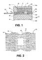
- FIG. 1is a cross-sectional view of two adjacent packages of a module of the present invention
- FIG. 2is a top planar view of a typical lead carrier of the present invention
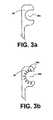
- FIG. 3 aillustrates the preferred embodiment for an aperture for connection with a package lead of the present invention
- FIG. 3 billustrates an alternative embodiment of an aperture for connection with a package lead of the present invention
- FIG. 4illustrates a horizontally stacked module of the present invention
- FIG. 5illustrates a vertically stacked module of the present invention
- FIG. 6illustrates an alternative embodiment of a horizontally stacked module of the present invention.
- FIG. 7illustrates an alternative embodiment of horizontally stacked module of the present invention.
- the letter of a reference character containing numerics followed by a lettereither identifies the relative placement of the referenced element within a stacked module or it identifies a specific embodiment.
- a typical ball-grid-array package 50is comprised of an integrated circuit 51 surrounded by an essentially rectangular solid resin casing 55 .
- Package leads 52extend from the bottom surface 54 of the casing in a two-dimensional grid pattern providing electrical and thermal coupling to one or more integrated circuit die 51 that are embedded within the protective casing.
- the external portion of each package lead 52includes a coating of solder having a semi-spherical shape.
- the protective casing 55completely surrounds the embedded die but, in some ball-grid-array packages 50 , the protective casing 55 does not cover the inactive top surface 53 of the die.
- Near-chip scale packages 50provide 1.0 mm center-to-center spacing between leads 52 .
- Chip scale packagingsuch as MICRO_BGATM have center-to-center lead spacing of 0.5 mm. Chip scale packaging offers excellent electrical characteristics including low capacitance and thermal design.
- FIGS. 4 through 7show various specific embodiments of stacked module M of the present invention.
- the letter Mdesignates the module M formed of a plurality of ball-grid-array packages 50 .
- the packages 50are aligned as shown in FIGS. 4 , 5 and 7 where the bottom surfaces 54 of each package 50 are facing the same direction.
- the packages 50may be aligned where one or more of the packages 50 are inverted in relation to the other packages 50 as shown in FIG. 6 .
- the top package 50 dis inverted with respect to the bottom package 50 e ; the top surface 56 of the top package 50 d is in substantially full contact with the adhesive 70 on the top surface 56 of the lower package 50 e.
- FIG. 1illustrates a partial cross-section of any two adjacent packages 50 that comprise a module M.
- the internals of package 50 bare not shown for simplicity.
- FIG. 1shows two packages 50 a and 50 b mounted on opposite sides of a lead carrier 60 comprised of a single thin copper plane.
- Interconnect leads 64extend away from the module M to provide external circuit connectivity to package leads 52 of the top package 50 a .
- External connectivitymay be provided in different configurations as described in detail below with reference to FIGS. 4-7 .
- FIG. 2A typical layout of a single plane lead carrier 60 is shown in FIG. 2 .
- the lead carrier 60is made to be flexible for increased reliability and ease of assembly.
- a lead carrier 60can be comprised of elongated conductive elements 65 formed from a thermally and electrically conductive thin planer material such as beryllium copper alloy C3 having a thickness of about 3 mils. Each conductive element 65 is defined to include a trace, interconnect pad, via and any other conductive feature of the lead carrier that are electrically coupled. Other preferred alloys for the lead-carrier-conductive elements 65 are full hard or hard copper alloys (110 or 197) or olin copper alloy 1094. Preferably, the lead carrier 60 is formed from custom flexible circuits from 3MTM and other manufacturers.
- These well known flexible circuitsare typically comprised of one or more thin (1.4 mils thick) layers of conductive material that are die cut and drilled to form apertures 66 , ground planes and conductive elements 65 which include traces, mounting pads and leads.
- the conductive layerstypically are flanked by a thin (typically 1 to 11 mils thick) layer of electrically-insulating, high-dielectric materials such at polyamide, polyester or teflon which results in circuit composites that are flexible.
- the material and thickness of individual layers that comprise the lead carriers 60 as well as spacing between conductive elements 65 and the width of conductive elements 65can be precisely controlled to provide accurate and consistent impedance control in select conductive elements 65 .
- Lead carriers 60 formed from custom flexible-circuitscan have vias for connecting traces located on different planes and conductive pads (or leads), with solder coating having footprints that are compatible with standards for ball-grid array packages 50 for electrical and mechanical coupling to a printed wiring board 80 .
- each conductive element 65 in a lead carrier 60has at least one aperture 66 , adapted to receive an individual package lead 52 and at least one interconnect portion 64 that extends away from the module to provide an external point of electrical connection to package leads 52 .
- Interconnect portions 64preferably have a spring-like resiliency for increased reliability.
- Apertures 66have about the same diameter as a package lead 52 allowing each package lead 52 to extend through the aperture 66 and for the lead carrier 60 to have substantial contact with the bottom surface 54 of a package 50 .
- FIG. 3 aillustrates the preferred semi-circle shape 66 a for the aperture 66 where the conductive element 65 partially surrounds the package lead 52 .
- the semicircle shape 66 aas opposed to a full-circle shape, enables an increased space for routing the conductive elements 65 of the lead carrier 60 .
- the present inventionutilizes standard manufactured packages 50 to form the multi-package module M.
- packages 50typically have package lead 52 irregularities or inconsistencies, particularly, lead length and solder coating variations. These variations make automated assembly problematic since the tolerances necessary to accommodate variation in lead 52 length, for example, do not permit the packages 50 to be assembled within the more stringent requirements for automated assembly of the module M.
- the package leads 52typically have excess solder that can cause electrical shorts between package leads 52 .
- the leads 52 of the ball-grid-array packages 50are scythed prior to assembly or as an automated step during the assembly after the lead carrier 60 is attached. Scything is the preferred method of reducing the length by which package leads 52 extend from the package 50 . Scything is a method where a hot razor knife skims off the distal portion of all package leads 52 .
- the adhesive 70may be epoxy, such as Rogers Corp. R/flex 8970 which is B-staged phenolic butyryl epoxy, that may be laminated at a temperature of 130 degrees centigrade and cured at a temperature of about 175 degrees centigrade.
- the preferred methodis to use a 2 mil thick sandwich of polyamide film 70 , such as KaptonTM which includes a 0.5 mil thick layer of adhesive on both sides (a three-layer system).
- a thermally conductive filled adhesive 70may be used to enhance the transfer of heat between adjacent packages 50 , and between the packages 50 and carrier 60 .
- a horizontally oriented embodiment of the present inventionis illustrated.
- a module Mis preassembled and then attached to a PWB 80 or other circuit carrying substrate.
- the preassembled module Mmay be inserted into an integrated circuit socket.
- each lead carrier 60has external interconnect portions 64 which extend from both sides of the module M to provide interconnection to an electrically and thermally conductive external interconnect structure 40 .
- Structure 40provides mechanical rigidity to the module M and is adhered to the upper surface 56 of the uppermost package 50 .
- Structure 40also includes circuit board interconnection portions 43 which may be formed for industry-standard socketability with an electrical socket carried in circuit board substrate 80 .
- FIG. 5A vertically-oriented configuration of module M is illustrated in FIG. 5 .
- lead carriers 60are formed with external interconnect portions 64 all extending to one side which requires the conductive elements 65 to be more densely spaced.
- external interconnect portions 64are spaced in row and column configuration for socketing or soldering to circuit connections on circuit board substrate 80 .
- module Mis formed in a two-high stack comprised of packages 50 e and 50 d .
- package 50 ehas its package leads 52 mounted directly to corresponding array of external circuit connect pads carried in substrate 80 .
- Upper package 50 dis inverted with respect to package 50 e and mounted to package 50 e with thermally conductive adhesive layer 70 .
- Surface 54 of package 50 dincludes package leads 52 .
- a lead carrier 60formed as described above, is adhered to surface 54 of package 50 d with thermally conductive adhesive 70
- External circuit interconnect portions 64provide electrical connectivity for upper package 50 d to circuit connection pads carried in substrate 80 .
- module Mis shown in an alternative three-high configuration comprised of individual packages 50 a , 50 b and 50 c .
- a lead carrier 60is adhered to the package surface 54 of each package.
- package leads 52are not shown as to packages 50 a and 50 b .
- Lead carriers 60 for packages 50 a and 50 binclude external circuit connect portions 64 b which are formed to nest together to provide mechanical rigidity and electrical and thermal conductivity for the module M.
- Lower package 50 chas lead carrier 60 c adhered to its lower surface 54 in the manner described above with thermally conductive, electrically insulating adhesive.
- circuit connection portions 64 a of lead carrier 60 care selectively interconnected to connection portions 64 b .
- Package leads 52 of lower package 50 care connected to external circuit connections carried in substrate 80 in a standard ball-grid-array pattern.
- a method for manufacture of a module Minvolves the following steps: (1) mounting an adhesive 70 a to the bottom surface 54 of a package 50 ; (2) aligning and mounting a lead carrier 60 to the adhesive 70 wherein apertures 66 receive the package leads 52 ; (3) scything of the distal end of all package leads 52 ; (4) applying heat (about 175 degrees centigrade) to cure adhesive 70 and flow the package lead 52 solder coating; (5) mounting a second thin layer of adhesive 70 b to the lead carrier 60 ; and (6) mounting another package 50 to the adhesive 70 b , wherein the top surface 56 of the package 50 has substantial contact with the adhesive. Steps 1 though 6 are repeated for each package 50 added to the module, except steps 5 and 6 are not repeated for the last package 50 . For reliability and remanufacturability, it may be desirable to test each package 50 as it is added to the module M.
- the preferred methodreplaces the steps of applying adhesive 70 a and 70 b with the preliminary step of applying double-sided adhesive tape 70 to both upper and lower surfaces of each lead carrier 60 prior to assembly.
- the step of applying heat to cause the solder to flow and to cure adhesive 70 after each step of mounting a package 50is eliminated if the leads 52 of the package 50 are reduced in height prior to assembly and a thin area of the second layer of adhesive 70 b around each aperture 66 is left void to allow the package leads 52 to form a flange when heat is applied.
- the module Mmay be assembled using a suitably formed manufacturing jig provided to hold individual packages 50 in alignment as they are stacked together with interspaced lead carriers 60 and adhesive carrying tape 70 . In this embodiment, the entire module M may be preassembled and a single heating event applied to flow the solder and cure the adhesive 70 as pressure is exerted on the module M to compress the layers.
- FIG. 3 ban alternative embodiment which compensates for excess solder steps utilizes channels 66 c formed in each aperture 66 b .
- FIG. 3 billustrates one shape of an aperture 66 b with multiple channels 66 c .
- a channel 66 cis a void area in a conductive element 65 which merges into the void area of an aperture 66 .
- an edge of each channel 66 cis in close proximity to the package leads 52 .
- the void area of the channel 66 cextends away from the ball 52 .
- the external structure 40may be formed integral to the leads 64 extending from the lead carrier 60 as shown in FIGS. 6 and 7 .
- the leads 64 bare formed such to electrically and thermally connect directly to selected adjacent leads 64 b .
- Leads 64may be formed with a substrate mounting portion that may have a standard “gull-wing,” “J-lead” shape.
Landscapes
- Engineering & Computer Science (AREA)
- Power Engineering (AREA)
- Microelectronics & Electronic Packaging (AREA)
- Physics & Mathematics (AREA)
- Condensed Matter Physics & Semiconductors (AREA)
- General Physics & Mathematics (AREA)
- Computer Hardware Design (AREA)
- Structures For Mounting Electric Components On Printed Circuit Boards (AREA)
- Lead Frames For Integrated Circuits (AREA)
Abstract
Description
Claims (13)
Priority Applications (2)
| Application Number | Priority Date | Filing Date | Title |
|---|---|---|---|
| US09/761,210US6919626B2 (en) | 1992-12-11 | 2001-01-16 | High density integrated circuit module |
| US11/040,564US20050139980A1 (en) | 1992-12-11 | 2005-01-21 | High density integrated circuit module |
Applications Claiming Priority (5)
| Application Number | Priority Date | Filing Date | Title |
|---|---|---|---|
| US07/990,334US5484959A (en) | 1992-12-11 | 1992-12-11 | High density lead-on-package fabrication method and apparatus |
| US08/497,565US5631193A (en) | 1992-12-11 | 1995-06-30 | High density lead-on-package fabrication method |
| US77469996A | 1996-12-26 | 1996-12-26 | |
| US09/222,263US6205654B1 (en) | 1992-12-11 | 1998-12-28 | Method of manufacturing a surface mount package |
| US09/761,210US6919626B2 (en) | 1992-12-11 | 2001-01-16 | High density integrated circuit module |
Related Parent Applications (2)
| Application Number | Title | Priority Date | Filing Date |
|---|---|---|---|
| US77469996AContinuation-In-Part | 1992-12-11 | 1996-12-26 | |
| US09/222,263DivisionUS6205654B1 (en) | 1992-12-11 | 1998-12-28 | Method of manufacturing a surface mount package |
Related Child Applications (1)
| Application Number | Title | Priority Date | Filing Date |
|---|---|---|---|
| US11/040,564ContinuationUS20050139980A1 (en) | 1992-12-11 | 2005-01-21 | High density integrated circuit module |
Publications (2)
| Publication Number | Publication Date |
|---|---|
| US20010005042A1 US20010005042A1 (en) | 2001-06-28 |
| US6919626B2true US6919626B2 (en) | 2005-07-19 |
Family
ID=27414069
Family Applications (2)
| Application Number | Title | Priority Date | Filing Date |
|---|---|---|---|
| US09/222,263Expired - LifetimeUS6205654B1 (en) | 1992-12-11 | 1998-12-28 | Method of manufacturing a surface mount package |
| US09/761,210Expired - Fee RelatedUS6919626B2 (en) | 1992-12-11 | 2001-01-16 | High density integrated circuit module |
Family Applications Before (1)
| Application Number | Title | Priority Date | Filing Date |
|---|---|---|---|
| US09/222,263Expired - LifetimeUS6205654B1 (en) | 1992-12-11 | 1998-12-28 | Method of manufacturing a surface mount package |
Country Status (1)
| Country | Link |
|---|---|
| US (2) | US6205654B1 (en) |
Cited By (56)
| Publication number | Priority date | Publication date | Assignee | Title |
|---|---|---|---|---|
| US20040229402A1 (en)* | 2001-10-26 | 2004-11-18 | Staktek Group, L.P. | Low profile chip scale stacking system and method |
| US20050062144A1 (en)* | 2001-10-26 | 2005-03-24 | Staktek Group, L.P. | Memory expansion and chip scale stacking system and method |
| US20060053345A1 (en)* | 2004-09-03 | 2006-03-09 | Staktek Group L.P. | Thin module system and method |
| US7033861B1 (en) | 2005-05-18 | 2006-04-25 | Staktek Group L.P. | Stacked module systems and method |
| US20060090102A1 (en)* | 2004-09-03 | 2006-04-27 | Wehrly James D Jr | Circuit module with thermal casing systems and methods |
| US20060091529A1 (en)* | 2004-09-03 | 2006-05-04 | Staktek Group L.P. | High capacity thin module system and method |
| US7053478B2 (en) | 2001-10-26 | 2006-05-30 | Staktek Group L.P. | Pitch change and chip scale stacking system |
| US20060129888A1 (en)* | 2004-09-03 | 2006-06-15 | Staktek Group L.P. | Circuit module turbulence enhacement systems and methods |
| US7081373B2 (en) | 2001-12-14 | 2006-07-25 | Staktek Group, L.P. | CSP chip stack with flex circuit |
| US20070006453A1 (en)* | 2005-07-07 | 2007-01-11 | Matsushita Electric Industrial Co., Ltd. | Component mounting apparatus and component mounting method |
| US20070006454A1 (en)* | 2005-07-07 | 2007-01-11 | Matsushita Electric Industrial Co., Ltd. | Component mounting apparatus and component mounting method |
| US7180167B2 (en) | 2001-10-26 | 2007-02-20 | Staktek Group L. P. | Low profile stacking system and method |
| US7202555B2 (en) | 2001-10-26 | 2007-04-10 | Staktek Group L.P. | Pitch change and chip scale stacking system and method |
| USRE39628E1 (en) | 1999-05-05 | 2007-05-15 | Stakick Group, L.P. | Stackable flex circuit IC package and method of making same |
| US20070222057A1 (en)* | 2006-03-23 | 2007-09-27 | Lai Yin M | Perpendicularly oriented electrically active element method and system |
| US7289327B2 (en) | 2006-02-27 | 2007-10-30 | Stakick Group L.P. | Active cooling methods and apparatus for modules |
| US7304382B2 (en) | 2006-01-11 | 2007-12-04 | Staktek Group L.P. | Managed memory component |
| US7309914B2 (en) | 2005-01-20 | 2007-12-18 | Staktek Group L.P. | Inverted CSP stacking system and method |
| US7310458B2 (en) | 2001-10-26 | 2007-12-18 | Staktek Group L.P. | Stacked module systems and methods |
| US20080020512A1 (en)* | 2002-10-08 | 2008-01-24 | Marcos Karnezos | Method for making a semiconductor multi-package module having inverted wire bond carrier second package |
| US7324352B2 (en) | 2004-09-03 | 2008-01-29 | Staktek Group L.P. | High capacity thin module system and method |
| US7335975B2 (en) | 2001-10-26 | 2008-02-26 | Staktek Group L.P. | Integrated circuit stacking system and method |
| US20080048309A1 (en)* | 2006-08-28 | 2008-02-28 | Corisis David J | Metal core foldover package structures, systems including same and methods of fabrication |
| US7371609B2 (en) | 2001-10-26 | 2008-05-13 | Staktek Group L.P. | Stacked module systems and methods |
| US20080122113A1 (en)* | 2006-08-17 | 2008-05-29 | Corisis David J | Semiconductor device assemblies and systems including at least one conductive pathway extending around a side of at least one semiconductor device and methods for forming the same |
| US20080157324A1 (en)* | 2006-12-28 | 2008-07-03 | Jia Miao Tang | Stacked die package with die interconnects |
| US7417310B2 (en) | 2006-11-02 | 2008-08-26 | Entorian Technologies, Lp | Circuit module having force resistant construction |
| US7423885B2 (en) | 2004-09-03 | 2008-09-09 | Entorian Technologies, Lp | Die module system |
| US7468893B2 (en) | 2004-09-03 | 2008-12-23 | Entorian Technologies, Lp | Thin module system and method |
| US7468553B2 (en) | 2006-10-20 | 2008-12-23 | Entorian Technologies, Lp | Stackable micropackages and stacked modules |
| US7480152B2 (en) | 2004-09-03 | 2009-01-20 | Entorian Technologies, Lp | Thin module system and method |
| US20090027863A1 (en)* | 2003-04-04 | 2009-01-29 | Marcos Karnezos | Method for making a semiconductor multipackage module including a processor and memory package assemblies |
| US7485951B2 (en) | 2001-10-26 | 2009-02-03 | Entorian Technologies, Lp | Modularized die stacking system and method |
| US7508069B2 (en) | 2006-01-11 | 2009-03-24 | Entorian Technologies, Lp | Managed memory component |
| US7508058B2 (en) | 2006-01-11 | 2009-03-24 | Entorian Technologies, Lp | Stacked integrated circuit module |
| US7511969B2 (en) | 2006-02-02 | 2009-03-31 | Entorian Technologies, Lp | Composite core circuit module system and method |
| US7511968B2 (en) | 2004-09-03 | 2009-03-31 | Entorian Technologies, Lp | Buffered thin module system and method |
| US7522421B2 (en) | 2004-09-03 | 2009-04-21 | Entorian Technologies, Lp | Split core circuit module |
| US7524703B2 (en) | 2001-10-26 | 2009-04-28 | Entorian Technologies, Lp | Integrated circuit stacking system and method |
| US20090109636A1 (en)* | 2007-10-25 | 2009-04-30 | Chipstack, Inc. | Multiple package module using a rigid flex printed circuit board |
| US7542297B2 (en) | 2004-09-03 | 2009-06-02 | Entorian Technologies, Lp | Optimized mounting area circuit module system and method |
| US7542304B2 (en) | 2003-09-15 | 2009-06-02 | Entorian Technologies, Lp | Memory expansion and integrated circuit stacking system and method |
| RU2364006C1 (en)* | 2008-03-14 | 2009-08-10 | Московский государственный институт электронной техники (технический университет) | Method for production of three-dimensional hybrid integral module |
| US7576995B2 (en) | 2005-11-04 | 2009-08-18 | Entorian Technologies, Lp | Flex circuit apparatus and method for adding capacitance while conserving circuit board surface area |
| US7606050B2 (en) | 2004-09-03 | 2009-10-20 | Entorian Technologies, Lp | Compact module system and method |
| US7606049B2 (en) | 2004-09-03 | 2009-10-20 | Entorian Technologies, Lp | Module thermal management system and method |
| US7606040B2 (en) | 2004-09-03 | 2009-10-20 | Entorian Technologies, Lp | Memory module system and method |
| US7605454B2 (en) | 2006-01-11 | 2009-10-20 | Entorian Technologies, Lp | Memory card and method for devising |
| US7608920B2 (en) | 2006-01-11 | 2009-10-27 | Entorian Technologies, Lp | Memory card and method for devising |
| US7616452B2 (en) | 2004-09-03 | 2009-11-10 | Entorian Technologies, Lp | Flex circuit constructions for high capacity circuit module systems and methods |
| USRE41039E1 (en) | 2000-01-13 | 2009-12-15 | Entorian Technologies, Lp | Stackable chip package with flex carrier |
| US7656678B2 (en) | 2001-10-26 | 2010-02-02 | Entorian Technologies, Lp | Stacked module systems |
| US7719098B2 (en) | 2001-10-26 | 2010-05-18 | Entorian Technologies Lp | Stacked modules and method |
| US7760513B2 (en) | 2004-09-03 | 2010-07-20 | Entorian Technologies Lp | Modified core for circuit module system and method |
| US20100246144A1 (en)* | 2006-01-25 | 2010-09-30 | Nec Corporation | Electronic device package, module, and electronic device |
| US9281302B2 (en) | 2014-02-20 | 2016-03-08 | International Business Machines Corporation | Implementing inverted master-slave 3D semiconductor stack |
Families Citing this family (40)
| Publication number | Priority date | Publication date | Assignee | Title |
|---|---|---|---|---|
| US5484959A (en)* | 1992-12-11 | 1996-01-16 | Staktek Corporation | High density lead-on-package fabrication method and apparatus |
| US6205654B1 (en)* | 1992-12-11 | 2001-03-27 | Staktek Group L.P. | Method of manufacturing a surface mount package |
| US6404662B1 (en)* | 1998-03-23 | 2002-06-11 | Staktek Group, L.P. | Rambus stakpak |
| US6153929A (en)* | 1998-08-21 | 2000-11-28 | Micron Technology, Inc. | Low profile multi-IC package connector |
| IL143962A0 (en)* | 1999-01-08 | 2002-04-21 | Emisphere Tech Inc | Polymeric delivery agents and delivery agent compounds |
| US6572387B2 (en) | 1999-09-24 | 2003-06-03 | Staktek Group, L.P. | Flexible circuit connector for stacked chip module |
| US6660561B2 (en)* | 2000-06-15 | 2003-12-09 | Dpac Technologies Corp. | Method of assembling a stackable integrated circuit chip |
| US6608763B1 (en) | 2000-09-15 | 2003-08-19 | Staktek Group L.P. | Stacking system and method |
| DE10060438B4 (en)* | 2000-12-05 | 2004-09-09 | Infineon Technologies Ag | Test arrangement for parallel testing of a plurality of integrated circuits and test methods |
| US6462408B1 (en) | 2001-03-27 | 2002-10-08 | Staktek Group, L.P. | Contact member stacking system and method |
| US20050009234A1 (en)* | 2001-10-26 | 2005-01-13 | Staktek Group, L.P. | Stacked module systems and methods for CSP packages |
| US20050056921A1 (en)* | 2003-09-15 | 2005-03-17 | Staktek Group L.P. | Stacked module systems and methods |
| US6576992B1 (en) | 2001-10-26 | 2003-06-10 | Staktek Group L.P. | Chip scale stacking system and method |
| US20040195666A1 (en)* | 2001-10-26 | 2004-10-07 | Julian Partridge | Stacked module systems and methods |
| US6731011B2 (en) | 2002-02-19 | 2004-05-04 | Matrix Semiconductor, Inc. | Memory module having interconnected and stacked integrated circuits |
| DE10259221B4 (en)* | 2002-12-17 | 2007-01-25 | Infineon Technologies Ag | Electronic component comprising a stack of semiconductor chips and method of making the same |
| US7191516B2 (en)* | 2003-07-16 | 2007-03-20 | Maxwell Technologies, Inc. | Method for shielding integrated circuit devices |
| US20060033187A1 (en)* | 2004-08-12 | 2006-02-16 | Staktek Group, L.P. | Rugged CSP module system and method |
| US20060043558A1 (en)* | 2004-09-01 | 2006-03-02 | Staktek Group L.P. | Stacked integrated circuit cascade signaling system and method |
| US20060261449A1 (en)* | 2005-05-18 | 2006-11-23 | Staktek Group L.P. | Memory module system and method |
| US20060049513A1 (en)* | 2004-09-03 | 2006-03-09 | Staktek Group L.P. | Thin module system and method with thermal management |
| US20060055024A1 (en)* | 2004-09-14 | 2006-03-16 | Staktek Group, L.P. | Adapted leaded integrated circuit module |
| US20060071316A1 (en)* | 2004-09-24 | 2006-04-06 | Emory Garth | Three-dimensional stack manufacture for integrated circuit devices and method of manufacture |
| US20060072297A1 (en)* | 2004-10-01 | 2006-04-06 | Staktek Group L.P. | Circuit Module Access System and Method |
| US20060118936A1 (en)* | 2004-12-03 | 2006-06-08 | Staktek Group L.P. | Circuit module component mounting system and method |
| US20060175693A1 (en)* | 2005-02-04 | 2006-08-10 | Staktek Group, L.P. | Systems, methods, and apparatus for generating ball-out matrix configuration output for a flex circuit |
| US20060244114A1 (en)* | 2005-04-28 | 2006-11-02 | Staktek Group L.P. | Systems, methods, and apparatus for connecting a set of contacts on an integrated circuit to a flex circuit via a contact beam |
| US20060250780A1 (en)* | 2005-05-06 | 2006-11-09 | Staktek Group L.P. | System component interposer |
| US20070158821A1 (en)* | 2006-01-11 | 2007-07-12 | Leland Szewerenko | Managed memory component |
| US20070164416A1 (en)* | 2006-01-17 | 2007-07-19 | James Douglas Wehrly | Managed memory component |
| US20070262429A1 (en)* | 2006-05-15 | 2007-11-15 | Staktek Group, L.P. | Perimeter stacking system and method |
| US20080203566A1 (en)* | 2007-02-27 | 2008-08-28 | Chao-Yuan Su | Stress buffer layer for packaging process |
| US8863046B2 (en)* | 2008-04-11 | 2014-10-14 | International Business Machines Corporation | Controlling impedance and thickness variations for multilayer electronic structures |
| US7921403B2 (en)* | 2008-04-11 | 2011-04-05 | International Business Machines Corporation | Controlling impedance and thickness variations for multilayer electronic structures |
| US8549444B2 (en)* | 2008-04-11 | 2013-10-01 | International Business Machines Corporation | Controlling impedance and thickness variations for multilayer electronic structures |
| US20100200949A1 (en) | 2009-02-12 | 2010-08-12 | International Business Machines Corporation | Method for tuning the threshold voltage of a metal gate and high-k device |
| WO2010104610A2 (en)* | 2009-03-13 | 2010-09-16 | Tessera Technologies Hungary Kft. | Stacked microelectronic assemblies having vias extending through bond pads |
| US8611090B2 (en) | 2010-09-09 | 2013-12-17 | International Business Machines Corporation | Electronic module with laterally-conducting heat distributor layer |
| US8779585B2 (en) | 2011-08-05 | 2014-07-15 | International Business Machines Corporation | Implementing enhanced thermal conductivity in stacked modules |
| CN112904180B (en)* | 2021-01-22 | 2022-04-19 | 长鑫存储技术有限公司 | Chip test board and chip test method |
Citations (226)
| Publication number | Priority date | Publication date | Assignee | Title |
|---|---|---|---|---|
| US3246386A (en) | 1962-01-26 | 1966-04-19 | Corning Glass Works | Electrical connected component and method |
| US3287606A (en) | 1964-12-16 | 1966-11-22 | Sperry Rand Corp | Packaging device for readily receiving and removing electrical components having a plurality of connecting leads |
| US3290559A (en) | 1964-06-16 | 1966-12-06 | Internat Energy Conversion Inc | Modular assembly for functional electronic blocks |
| US3313986A (en) | 1959-05-06 | 1967-04-11 | Texas Instruments Inc | Interconnecting miniature circuit modules |
| US3377516A (en) | 1966-08-04 | 1968-04-09 | Hughes Aircraft Co | Cordwood package with removable plugs |
| US3403300A (en) | 1966-09-01 | 1968-09-24 | Magnavox Co | Electronic module |
| US3436604A (en) | 1966-04-25 | 1969-04-01 | Texas Instruments Inc | Complex integrated circuit array and method for fabricating same |
| US3515949A (en) | 1967-11-22 | 1970-06-02 | Bunker Ramo | 3-d flatpack module packaging technique |
| US3535595A (en) | 1967-11-09 | 1970-10-20 | Ferroxcube Corp | Universal cord-wood module |
| US3614541A (en) | 1969-04-08 | 1971-10-19 | North American Rockwell | Package for an electronic assembly |
| US3614546A (en) | 1970-01-07 | 1971-10-19 | Rca Corp | Shielded semiconductor device |
| US3671812A (en) | 1970-07-01 | 1972-06-20 | Martin Marietta Corp | High density packaging of electronic components in three-dimensional modules |
| US3713893A (en) | 1969-11-20 | 1973-01-30 | Gould Inc | Integrated solar cell array |
| US3727064A (en) | 1971-03-17 | 1973-04-10 | Monsanto Co | Opto-isolator devices and method for the fabrication thereof |
| US3739462A (en) | 1971-01-06 | 1973-06-19 | Texas Instruments Inc | Method for encapsulating discrete semiconductor chips |
| US3746934A (en) | 1971-05-06 | 1973-07-17 | Siemens Ag | Stack arrangement of semiconductor chips |
| US3772776A (en) | 1969-12-03 | 1973-11-20 | Thomas & Betts Corp | Method of interconnecting memory plane boards |
| US3925801A (en) | 1972-02-14 | 1975-12-09 | Hewlett Packard Co | Photon isolator with improved photodetector transistor stage |
| US3949274A (en) | 1974-05-30 | 1976-04-06 | International Business Machines Corporation | Packaging and interconnection for superconductive circuitry |
| US3959579A (en) | 1974-08-19 | 1976-05-25 | International Business Machines Corporation | Apertured semi-conductor device mounted on a substrate |
| US4017963A (en) | 1973-02-26 | 1977-04-19 | Signetics Corporation | Semiconductor assembly and method |
| US4103318A (en) | 1977-05-06 | 1978-07-25 | Ford Motor Company | Electronic multichip module |
| US4116519A (en) | 1977-08-02 | 1978-09-26 | Amp Incorporated | Electrical connections for chip carriers |
| US4116518A (en) | 1977-08-31 | 1978-09-26 | Ncr Corporation | Clip for paralleling packaged integrated circuit chips |
| US4139726A (en) | 1978-01-16 | 1979-02-13 | Allen-Bradley Company | Packaged microcircuit and method for assembly thereof |
| US4158745A (en) | 1977-10-27 | 1979-06-19 | Amp Incorporated | Lead frame having integral terminal tabs |
| US4241493A (en) | 1978-12-22 | 1980-12-30 | Andrulitis William B | Method of fabricating solar cell modules |
| SU834957A1 (en) | 1979-03-12 | 1981-05-30 | Предприятие П/Я А-7438 | Device for feeding printed circuit boards |
| US4288841A (en) | 1979-09-20 | 1981-09-08 | Bell Telephone Laboratories, Incorporated | Double cavity semiconductor chip carrier |
| US4288808A (en) | 1978-01-28 | 1981-09-08 | International Computers Limited | Circuit structures including integrated circuits |
| JPS5731166A (en) | 1980-07-31 | 1982-02-19 | Fujitsu Ltd | Semiconductor device |
| US4321418A (en) | 1979-05-08 | 1982-03-23 | Saint Gobain Vitrage | Process for manufacture of solar photocell panels and panels obtained thereby |
| US4331258A (en) | 1981-03-05 | 1982-05-25 | Raychem Corporation | Sealing cover for an hermetically sealed container |
| US4364620A (en) | 1980-09-05 | 1982-12-21 | Mostek Corporation | Socket for housing a plurality of integrated circuits |
| US4371912A (en) | 1980-10-01 | 1983-02-01 | Motorola, Inc. | Method of mounting interrelated components |
| US4379259A (en) | 1980-03-12 | 1983-04-05 | National Semiconductor Corporation | Process of performing burn-in and parallel functional testing of integrated circuit memories in an environmental chamber |
| JPS5896756A (en) | 1981-12-04 | 1983-06-08 | Toshiba Corp | multi-chip package |
| JPS58112348A (en) | 1981-12-25 | 1983-07-04 | Fujitsu Ltd | semiconductor equipment |
| US4394712A (en) | 1981-03-18 | 1983-07-19 | General Electric Company | Alignment-enhancing feed-through conductors for stackable silicon-on-sapphire wafers |
| US4398235A (en) | 1980-09-11 | 1983-08-09 | General Motors Corporation | Vertical integrated circuit package integration |
| US4406508A (en) | 1981-07-02 | 1983-09-27 | Thomas & Betts Corporation | Dual-in-line package assembly |
| JPS58219757A (en) | 1982-06-16 | 1983-12-21 | Toshiba Corp | Semiconductor device |
| US4437235A (en) | 1980-12-29 | 1984-03-20 | Honeywell Information Systems Inc. | Integrated circuit package |
| US4451973A (en) | 1981-04-28 | 1984-06-05 | Matsushita Electronics Corporation | Method for manufacturing a plastic encapsulated semiconductor device and a lead frame therefor |
| US4521828A (en) | 1982-12-23 | 1985-06-04 | At&T Technologies, Inc. | Component module for piggyback mounting on a circuit package having dual-in-line leads |
| US4525921A (en) | 1981-07-13 | 1985-07-02 | Irvine Sensors Corporation | High-density electronic processing package-structure and fabrication |
| JPS60160641U (en) | 1984-03-30 | 1985-10-25 | カシオ計算機株式会社 | touch switch device |
| JPS60254762A (en) | 1984-05-31 | 1985-12-16 | Fujitsu Ltd | Semiconductor device package |
| US4571663A (en) | 1982-06-19 | 1986-02-18 | Ferranti Plc | Electrical circuit assemblies |
| US4574331A (en) | 1983-05-31 | 1986-03-04 | Trw Inc. | Multi-element circuit construction |
| JPS6175558A (en) | 1984-09-21 | 1986-04-17 | Nec Corp | Hybrid integrated circuit device |
| JPS6163048U (en) | 1984-09-29 | 1986-04-28 | ||
| US4587596A (en) | 1984-04-09 | 1986-05-06 | Amp Incorporated | High density mother/daughter circuit board connector |
| JPS61163652A (en) | 1985-01-15 | 1986-07-24 | Matsushita Electric Works Ltd | Semiconductor device |
| JPS61219143A (en) | 1985-03-25 | 1986-09-29 | Nec Corp | Manufacture of resin sealed type semiconductor device |
| US4630172A (en) | 1983-03-09 | 1986-12-16 | Printed Circuits International | Semiconductor chip carrier package with a heat sink |
| US4631573A (en) | 1985-05-24 | 1986-12-23 | Sundstrand Corporation | Cooled stack of electrically isolated semiconductors |
| US4633573A (en) | 1982-10-12 | 1987-01-06 | Aegis, Inc. | Microcircuit package and sealing method |
| US4638406A (en) | 1984-10-04 | 1987-01-20 | Motorola, Inc. | Discrete component mounting assembly |
| US4638348A (en) | 1982-08-10 | 1987-01-20 | Brown David F | Semiconductor chip carrier |
| US4642735A (en) | 1984-02-27 | 1987-02-10 | General Electric Company | Frequency synthesizer module |
| US4680617A (en) | 1984-05-23 | 1987-07-14 | Ross Milton I | Encapsulated electronic circuit device, and method and apparatus for making same |
| US4684975A (en) | 1985-12-16 | 1987-08-04 | National Semiconductor Corporation | Molded semiconductor package having improved heat dissipation |
| US4688864A (en) | 1985-04-05 | 1987-08-25 | U.S. Philips Corporation | Electronic circuit constituted by stackable modules |
| US4696525A (en) | 1985-12-13 | 1987-09-29 | Amp Incorporated | Socket for stacking integrated circuit packages |
| US4698663A (en) | 1986-09-17 | 1987-10-06 | Fujitsu Limited | Heatsink package for flip-chip IC |
| JPS62230027A (en) | 1986-03-31 | 1987-10-08 | Matsushita Electric Ind Co Ltd | Manufacture of semiconductor device |
| US4706166A (en) | 1986-04-25 | 1987-11-10 | Irvine Sensors Corporation | High-density electronic modules--process and product |
| US4712129A (en) | 1983-12-12 | 1987-12-08 | Texas Instruments Incorporated | Integrated circuit device with textured bar cover |
| US4722060A (en) | 1984-03-22 | 1988-01-26 | Thomson Components-Mostek Corporation | Integrated-circuit leadframe adapted for a simultaneous bonding operation |
| US4722691A (en) | 1986-02-03 | 1988-02-02 | General Motors Corporation | Header assembly for a printed circuit board |
| US4733461A (en) | 1984-12-28 | 1988-03-29 | Micro Co., Ltd. | Method of stacking printed circuit boards |
| JPS63117451A (en) | 1986-11-06 | 1988-05-21 | Oki Electric Ind Co Ltd | Semiconductor device |
| JPS63153849A (en) | 1986-12-17 | 1988-06-27 | Nec Corp | Semiconductor device |
| US4761681A (en) | 1982-09-08 | 1988-08-02 | Texas Instruments Incorporated | Method for fabricating a semiconductor contact and interconnect structure using orientation dependent etching and thermomigration |
| US4763188A (en) | 1986-08-08 | 1988-08-09 | Thomas Johnson | Packaging system for multiple semiconductor devices |
| US4764846A (en) | 1987-01-05 | 1988-08-16 | Irvine Sensors Corporation | High density electronic package comprising stacked sub-modules |
| US4770640A (en) | 1983-06-24 | 1988-09-13 | Walter Howard F | Electrical interconnection device for integrated circuits |
| US4796078A (en) | 1987-06-15 | 1989-01-03 | International Business Machines Corporation | Peripheral/area wire bonding technique |
| US4821007A (en) | 1987-02-06 | 1989-04-11 | Tektronix, Inc. | Strip line circuit component and method of manufacture |
| US4821148A (en) | 1985-06-14 | 1989-04-11 | Hitachi, Ltd. | Resin packaged semiconductor device having a protective layer made of a metal-organic matter compound |
| US4823234A (en) | 1985-08-16 | 1989-04-18 | Dai-Ichi Seiko Co., Ltd. | Semiconductor device and its manufacture |
| US4829403A (en) | 1987-01-20 | 1989-05-09 | Harding Ade Yemi S K | Packaging arrangement for energy dissipating devices |
| US4833568A (en) | 1988-01-29 | 1989-05-23 | Berhold G Mark | Three-dimensional circuit component assembly and method corresponding thereto |
| US4839717A (en) | 1986-12-19 | 1989-06-13 | Fairchild Semiconductor Corporation | Ceramic package for high frequency semiconductor devices |
| US4841355A (en) | 1988-02-10 | 1989-06-20 | Amdahl Corporation | Three-dimensional microelectronic package for semiconductor chips |
| US4855868A (en) | 1987-01-20 | 1989-08-08 | Harding Ade Yemi S K | Preformed packaging arrangement for energy dissipating devices |
| US4862245A (en) | 1985-04-18 | 1989-08-29 | International Business Machines Corporation | Package semiconductor chip |
| US4862249A (en) | 1987-04-17 | 1989-08-29 | Xoc Devices, Inc. | Packaging system for stacking integrated circuits |
| US4868712A (en) | 1987-02-04 | 1989-09-19 | Woodman John K | Three dimensional integrated circuit package |
| US4878106A (en) | 1986-12-02 | 1989-10-31 | Anton Piller Gmbh & Co. Kg | Semiconductor circuit packages for use in high power applications and method of making the same |
| US4884237A (en) | 1984-03-28 | 1989-11-28 | International Business Machines Corporation | Stacked double density memory module using industry standard memory chips |
| US4891789A (en) | 1988-03-03 | 1990-01-02 | Bull Hn Information Systems, Inc. | Surface mounted multilayer memory printed circuit board |
| US4911643A (en) | 1988-10-11 | 1990-03-27 | Beta Phase, Inc. | High density and high signal integrity connector |
| US4924352A (en) | 1987-12-22 | 1990-05-08 | Societe Anonyme Dite: Alcatel Cit | Method and device for cooling an integrated circuit package |
| US4948645A (en) | 1989-08-01 | 1990-08-14 | Rogers Corporation | Tape automated bonding and method of making the same |
| US4953060A (en) | 1989-05-05 | 1990-08-28 | Ncr Corporation | Stackable integrated circuit chip package with improved heat removal |
| US4953005A (en) | 1987-04-17 | 1990-08-28 | Xoc Devices, Inc. | Packaging system for stacking integrated circuits |
| US4956694A (en) | 1988-11-04 | 1990-09-11 | Dense-Pac Microsystems, Inc. | Integrated circuit chip stacking |
| JPH02260448A (en) | 1989-03-30 | 1990-10-23 | Mitsubishi Electric Corp | Semiconductor device and radiating fin |
| US4983533A (en) | 1987-10-28 | 1991-01-08 | Irvine Sensors Corporation | High-density electronic modules - process and product |
| EP0298211A3 (en) | 1987-07-06 | 1991-01-16 | International Business Machines Corporation | Ceramic card assembly having enhanced power distribution and cooling |
| US4994411A (en) | 1988-03-10 | 1991-02-19 | Hitachi, Ltd. | Process of producing semiconductor device |
| US4996587A (en) | 1989-04-10 | 1991-02-26 | International Business Machines Corporation | Integrated semiconductor chip package |
| US4996583A (en) | 1989-02-15 | 1991-02-26 | Matsushita Electric Industrial Co., Ltd. | Stack type semiconductor package |
| US4997517A (en) | 1990-01-09 | 1991-03-05 | Olin Corporation | Multi-metal layer interconnect tape for tape automated bonding |
| US5001545A (en) | 1988-09-09 | 1991-03-19 | Motorola, Inc. | Formed top contact for non-flat semiconductor devices |
| JPH0396266A (en) | 1989-09-08 | 1991-04-22 | Mitsubishi Electric Corp | Semiconductor integrated circuit module |
| US5012323A (en) | 1989-11-20 | 1991-04-30 | Micron Technology, Inc. | Double-die semiconductor package having a back-bonded die and a face-bonded die interconnected on a single leadframe |
| US5014113A (en) | 1989-12-27 | 1991-05-07 | Motorola, Inc. | Multiple layer lead frame |
| US5016138A (en) | 1987-10-27 | 1991-05-14 | Woodman John K | Three dimensional integrated circuit package |
| US5031072A (en) | 1986-08-01 | 1991-07-09 | Texas Instruments Incorporated | Baseboard for orthogonal chip mount |
| JPH03167868A (en) | 1989-11-28 | 1991-07-19 | Nec Corp | Integrated circuit device provided with shielding function; apparatus and method for its manufacture |
| US5034350A (en) | 1987-09-23 | 1991-07-23 | Sgs Thomson Microelectronics S.R.L. | Semiconductor device package with dies mounted on both sides of the central pad of a metal frame |
| US5041015A (en) | 1990-03-30 | 1991-08-20 | Cal Flex, Inc. | Electrical jumper assembly |
| US5041395A (en) | 1989-04-07 | 1991-08-20 | Sgs-Thomson Microelectronics S.A. | Method of encapsulating an integrated circuit using a punched metal grid attached to a perforated dielectric strip |
| US5043794A (en) | 1990-09-24 | 1991-08-27 | At&T Bell Laboratories | Integrated circuit package and compact assemblies thereof |
| US5049527A (en) | 1985-06-25 | 1991-09-17 | Hewlett-Packard Company | Optical isolator |
| US5057903A (en) | 1989-07-17 | 1991-10-15 | Microelectronics And Computer Technology Corporation | Thermal heat sink encapsulated integrated circuit |
| US5057906A (en) | 1989-05-22 | 1991-10-15 | Kabushiki Kaisha Toshiba | Plastic molded type semiconductor device |
| US5058265A (en) | 1990-05-10 | 1991-10-22 | Rockwell International Corporation | Method for packaging a board of electronic components |
| US5065277A (en) | 1990-07-13 | 1991-11-12 | Sun Microsystems, Inc. | Three dimensional packaging arrangement for computer systems and the like |
| US5068708A (en) | 1989-10-02 | 1991-11-26 | Advanced Micro Devices, Inc. | Ground plane for plastic encapsulated integrated circuit die packages |
| US5086018A (en) | 1991-05-02 | 1992-02-04 | International Business Machines Corporation | Method of making a planarized thin film covered wire bonded semiconductor package |
| US5099393A (en) | 1991-03-25 | 1992-03-24 | International Business Machines Corporation | Electronic package for high density applications |
| US5101324A (en) | 1989-03-02 | 1992-03-31 | Seiko Epson Corporation | Structure, method of, and apparatus for mounting semiconductor devices |
| US5104820A (en) | 1989-07-07 | 1992-04-14 | Irvine Sensors Corporation | Method of fabricating electronic circuitry unit containing stacked IC layers having lead rerouting |
| US5107328A (en) | 1991-02-13 | 1992-04-21 | Micron Technology, Inc. | Packaging means for a semiconductor die having particular shelf structure |
| US5108553A (en) | 1989-04-04 | 1992-04-28 | Olin Corporation | G-tab manufacturing process and the product produced thereby |
| US5128831A (en) | 1991-10-31 | 1992-07-07 | Micron Technology, Inc. | High-density electronic package comprising stacked sub-modules which are electrically interconnected by solder-filled vias |
| JPH04209562A (en) | 1990-12-06 | 1992-07-30 | Fujitsu Ltd | Module structure of semiconductor package |
| US5138430A (en) | 1991-06-06 | 1992-08-11 | International Business Machines Corporation | High performance versatile thermally enhanced IC chip mounting |
| US5138434A (en) | 1991-01-22 | 1992-08-11 | Micron Technology, Inc. | Packaging for semiconductor logic devices |
| US5140745A (en) | 1990-07-23 | 1992-08-25 | Mckenzie Jr Joseph A | Method for forming traces on side edges of printed circuit boards and devices formed thereby |
| US5151559A (en) | 1991-05-02 | 1992-09-29 | International Business Machines Corporation | Planarized thin film surface covered wire bonded semiconductor package |
| US5155068A (en) | 1989-08-31 | 1992-10-13 | Sharp Kabushiki Kaisha | Method for manufacturing an IC module for an IC card whereby an IC device and surrounding encapsulant are thinned by material removal |
| US5159434A (en) | 1990-02-01 | 1992-10-27 | Hitachi, Ltd. | Semiconductor device having a particular chip pad structure |
| US5168926A (en) | 1991-09-25 | 1992-12-08 | Intel Corporation | Heat sink design integrating interface material |
| US5198888A (en) | 1987-12-28 | 1993-03-30 | Hitachi, Ltd. | Semiconductor stacked device |
| US5200362A (en) | 1989-09-06 | 1993-04-06 | Motorola, Inc. | Method of attaching conductive traces to an encapsulated semiconductor die using a removable transfer film |
| US5214307A (en) | 1991-07-08 | 1993-05-25 | Micron Technology, Inc. | Lead frame for semiconductor devices having improved adhesive bond line control |
| US5214845A (en) | 1992-05-11 | 1993-06-01 | Micron Technology, Inc. | Method for producing high speed integrated circuits |
| US5221642A (en) | 1991-08-15 | 1993-06-22 | Staktek Corporation | Lead-on-chip integrated circuit fabrication method |
| US5222014A (en) | 1992-03-02 | 1993-06-22 | Motorola, Inc. | Three-dimensional multi-chip pad array carrier |
| US5223739A (en) | 1989-09-14 | 1993-06-29 | Kabushiki Kaisha Toshiba | Plastic molded semiconductor device having waterproof cap |
| US5231304A (en) | 1989-07-27 | 1993-07-27 | Grumman Aerospace Corporation | Framed chip hybrid stacked layer assembly |
| US5236117A (en) | 1992-06-22 | 1993-08-17 | Staktek Corporation | Impact solder method and apparatus |
| US5239447A (en) | 1991-09-13 | 1993-08-24 | International Business Machines Corporation | Stepped electronic device package |
| US5241454A (en) | 1992-01-22 | 1993-08-31 | International Business Machines Corporation | Mutlilayered flexible circuit package |
| US5243133A (en) | 1992-02-18 | 1993-09-07 | International Business Machines, Inc. | Ceramic chip carrier with lead frame or edge clip |
| US5247423A (en) | 1992-05-26 | 1993-09-21 | Motorola, Inc. | Stacking three dimensional leadless multi-chip module and method for making the same |
| US5252857A (en) | 1991-08-05 | 1993-10-12 | International Business Machines Corporation | Stacked DCA memory chips |
| US5259770A (en) | 1992-03-19 | 1993-11-09 | Amp Incorporated | Impedance controlled elastomeric connector |
| US5262927A (en) | 1992-02-07 | 1993-11-16 | Lsi Logic Corporation | Partially-molded, PCB chip carrier package |
| US5266834A (en) | 1989-03-13 | 1993-11-30 | Hitachi Ltd. | Semiconductor device and an electronic device with the semiconductor devices mounted thereon |
| US5273940A (en) | 1992-06-15 | 1993-12-28 | Motorola, Inc. | Multiple chip package with thinned semiconductor chips |
| US5279991A (en) | 1992-05-15 | 1994-01-18 | Irvine Sensors Corporation | Method for fabricating stacks of IC chips by segmenting a larger stack |
| US5279029A (en) | 1990-08-01 | 1994-01-18 | Staktek Corporation | Ultra high density integrated circuit packages method |
| US5281852A (en) | 1991-12-10 | 1994-01-25 | Normington Peter J C | Semiconductor device including stacked die |
| US5307929A (en) | 1991-06-19 | 1994-05-03 | North American Specialties Corporation | Lead arrangement for integrated circuits and method of assembly |
| US5311401A (en) | 1991-07-09 | 1994-05-10 | Hughes Aircraft Company | Stacked chip assembly and manufacturing method therefor |
| US5311060A (en) | 1989-12-19 | 1994-05-10 | Lsi Logic Corporation | Heat sink for semiconductor device assembly |
| US5313097A (en) | 1992-11-16 | 1994-05-17 | International Business Machines, Corp. | High density memory module |
| US5313096A (en) | 1992-03-16 | 1994-05-17 | Dense-Pac Microsystems, Inc. | IC chip package having chip attached to and wire bonded within an overlying substrate |
| US5343075A (en) | 1991-06-29 | 1994-08-30 | Sony Corporation | Composite stacked semiconductor device with contact plates |
| US5343366A (en) | 1992-06-24 | 1994-08-30 | International Business Machines Corporation | Packages for stacked integrated circuit chip cubes |
| US5347428A (en) | 1992-12-03 | 1994-09-13 | Irvine Sensors Corporation | Module comprising IC memory stack dedicated to and structurally combined with an IC microprocessor chip |
| US5347429A (en) | 1990-11-14 | 1994-09-13 | Hitachi, Ltd. | Plastic-molded-type semiconductor device |
| JPH0677644B2 (en) | 1986-01-22 | 1994-10-05 | 英和 栗本 | Stage switching operation type distillation device |
| US5369058A (en) | 1993-03-29 | 1994-11-29 | Staktek Corporation | Warp-resistent ultra-thin integrated circuit package fabrication method |
| US5367766A (en) | 1990-08-01 | 1994-11-29 | Staktek Corporation | Ultra high density integrated circuit packages method |
| US5371866A (en) | 1992-06-01 | 1994-12-06 | Staktek Corporation | Simulcast standard multichip memory addressing system |
| US5373189A (en) | 1992-08-13 | 1994-12-13 | Commissariate A L'energie Atomique | Three-dimensional multichip module |
| US5377077A (en) | 1990-08-01 | 1994-12-27 | Staktek Corporation | Ultra high density integrated circuit packages method and apparatus |
| US5384689A (en) | 1993-12-20 | 1995-01-24 | Shen; Ming-Tung | Integrated circuit chip including superimposed upper and lower printed circuit boards |
| US5394010A (en) | 1991-03-13 | 1995-02-28 | Kabushiki Kaisha Toshiba | Semiconductor assembly having laminated semiconductor devices |
| US5397916A (en) | 1991-12-10 | 1995-03-14 | Normington; Peter J. C. | Semiconductor device including stacked die |
| US5426566A (en) | 1991-09-30 | 1995-06-20 | International Business Machines Corporation | Multichip integrated circuit packages and systems |
| US5438224A (en) | 1992-04-23 | 1995-08-01 | Motorola, Inc. | Integrated circuit package having a face-to-face IC chip arrangement |
| US5446313A (en) | 1992-05-25 | 1995-08-29 | Hitachi, Ltd. | Thin type semiconductor device and module structure using the device |
| US5446620A (en) | 1990-08-01 | 1995-08-29 | Staktek Corporation | Ultra high density integrated circuit packages |
| US5477082A (en) | 1994-01-11 | 1995-12-19 | Exponential Technology, Inc. | Bi-planar multi-chip module |
| US5475920A (en) | 1990-08-01 | 1995-12-19 | Burns; Carmen D. | Method of assembling ultra high density integrated circuit packages |
| US5479318A (en) | 1994-03-07 | 1995-12-26 | Staktek Corporation | Bus communication system for stacked high density integrated circuit packages with trifurcated distal lead ends |
| US5481133A (en) | 1994-03-21 | 1996-01-02 | United Microelectronics Corporation | Three-dimensional multichip package |
| US5484959A (en) | 1992-12-11 | 1996-01-16 | Staktek Corporation | High density lead-on-package fabrication method and apparatus |
| US5499160A (en) | 1990-08-01 | 1996-03-12 | Staktek Corporation | High density integrated circuit module with snap-on rail assemblies |
| US5514907A (en) | 1995-03-21 | 1996-05-07 | Simple Technology Incorporated | Apparatus for stacking semiconductor chips |
| US5523619A (en) | 1993-11-03 | 1996-06-04 | International Business Machines Corporation | High density memory structure |
| US5588205A (en) | 1995-01-24 | 1996-12-31 | Staktek Corporation | Method of manufacturing a high density integrated circuit module having complex electrical interconnect rails |
| US5592364A (en) | 1995-01-24 | 1997-01-07 | Staktek Corporation | High density integrated circuit module with complex electrical interconnect rails |
| US5612570A (en) | 1995-04-13 | 1997-03-18 | Dense-Pac Microsystems, Inc. | Chip stack and method of making same |
| US5615475A (en) | 1995-01-30 | 1997-04-01 | Staktek Corporation | Method of manufacturing an integrated package having a pair of die on a common lead frame |
| US5644161A (en) | 1993-03-29 | 1997-07-01 | Staktek Corporation | Ultra-high density warp-resistant memory module |
| US5654877A (en) | 1991-08-15 | 1997-08-05 | Staktek Corporation | Lead-on-chip integrated circuit apparatus |
| US5657537A (en) | 1995-05-30 | 1997-08-19 | General Electric Company | Method for fabricating a stack of two dimensional circuit modules |
| US5778522A (en) | 1996-05-20 | 1998-07-14 | Staktek Corporation | Method of manufacturing a high density integrated circuit module with complex electrical interconnect rails having electrical interconnect strain relief |
| US5783464A (en) | 1992-06-26 | 1998-07-21 | Staktek Corporation | Method of forming a hermetically sealed circuit lead-on package |
| US5789815A (en) | 1996-04-23 | 1998-08-04 | Motorola, Inc. | Three dimensional semiconductor package having flexible appendages |
| US5801437A (en) | 1993-03-29 | 1998-09-01 | Staktek Corporation | Three-dimensional warp-resistant integrated circuit module method and apparatus |
| US5835988A (en) | 1996-03-27 | 1998-11-10 | Mitsubishi Denki Kabushiki Kaisha | Packed semiconductor device with wrap around external leads |
| US5917709A (en) | 1997-06-16 | 1999-06-29 | Eastman Kodak Company | Multiple circuit board assembly having an interconnect mechanism that includes a flex connector |
| US6014316A (en) | 1997-06-13 | 2000-01-11 | Irvine Sensors Corporation | IC stack utilizing BGA contacts |
| US6025642A (en) | 1995-08-17 | 2000-02-15 | Staktek Corporation | Ultra high density integrated circuit packages |
| US6028365A (en) | 1998-03-30 | 2000-02-22 | Micron Technology, Inc. | Integrated circuit package and method of fabrication |
| US6028352A (en) | 1997-06-13 | 2000-02-22 | Irvine Sensors Corporation | IC stack utilizing secondary leadframes |
| US6133637A (en) | 1997-01-24 | 2000-10-17 | Rohm Co., Ltd. | Semiconductor device having a plurality of semiconductor chips |
| US6153929A (en) | 1998-08-21 | 2000-11-28 | Micron Technology, Inc. | Low profile multi-IC package connector |
| US6157541A (en) | 1997-12-30 | 2000-12-05 | Siemens Aktiengesellschaft | Stack arrangement for two semiconductor memory chips and printed board for accepting a plurality of such stack arrangements |
| US6172874B1 (en) | 1998-04-06 | 2001-01-09 | Silicon Graphics, Inc. | System for stacking of integrated circuit packages |
| US6178093B1 (en) | 1996-06-28 | 2001-01-23 | International Business Machines Corporation | Information handling system with circuit assembly having holes filled with filler material |
| US6187652B1 (en) | 1998-09-14 | 2001-02-13 | Fujitsu Limited | Method of fabrication of multiple-layer high density substrate |
| US6205654B1 (en) | 1992-12-11 | 2001-03-27 | Staktek Group L.P. | Method of manufacturing a surface mount package |
| US6262476B1 (en) | 1998-07-27 | 2001-07-17 | Siemens Aktiengesellschaft | Composite member composed of at least two integrated circuits and method for the manufacture of a composite member composed of at least two integrated circuits |
| US6300679B1 (en) | 1998-06-01 | 2001-10-09 | Semiconductor Components Industries, Llc | Flexible substrate for packaging a semiconductor component |
| US6303981B1 (en) | 1999-09-01 | 2001-10-16 | Micron Technology, Inc. | Semiconductor package having stacked dice and leadframes and method of fabrication |
| US6310392B1 (en) | 1998-12-28 | 2001-10-30 | Staktek Group, L.P. | Stacked micro ball grid array packages |
| US6313998B1 (en) | 1999-04-02 | 2001-11-06 | Legacy Electronics, Inc. | Circuit board assembly having a three dimensional array of integrated circuit packages |
| US6316825B1 (en) | 1998-05-15 | 2001-11-13 | Hyundai Electronics Industries Co., Ltd. | Chip stack package utilizing a connecting hole to improve electrical connection between leadframes |
| US6323060B1 (en) | 1999-05-05 | 2001-11-27 | Dense-Pac Microsystems, Inc. | Stackable flex circuit IC package and method of making same |
| US6335565B1 (en) | 1996-12-04 | 2002-01-01 | Hitachi, Ltd. | Semiconductor device |
| US6376769B1 (en) | 1999-05-18 | 2002-04-23 | Amerasia International Technology, Inc. | High-density electronic package, and method for making same |
| US6426560B1 (en) | 1999-08-06 | 2002-07-30 | Hitachi, Ltd. | Semiconductor device and memory module |
| US6426240B2 (en) | 1999-05-05 | 2002-07-30 | Harlan R. Isaak | Stackable flex circuit chip package and method of making same |
| US6462408B1 (en) | 2001-03-27 | 2002-10-08 | Staktek Group, L.P. | Contact member stacking system and method |
| US6489687B1 (en) | 1999-10-01 | 2002-12-03 | Seiko Epson Corporation | Semiconductor device and method of manufacturing the same, manufacturing device, circuit board, and electronic equipment |
Family Cites Families (5)
| Publication number | Priority date | Publication date | Assignee | Title |
|---|---|---|---|---|
| US3315949A (en)* | 1965-10-22 | 1967-04-25 | Bendix Corp | Automatic choke |
| US4437236A (en)* | 1982-01-25 | 1984-03-20 | E. I. Du Pont De Nemours And Company | Solder bonding process |
| JPS60180150A (en) | 1984-02-27 | 1985-09-13 | Nippon Telegr & Teleph Corp <Ntt> | Semiconductor device |
| US4680172A (en) | 1985-03-05 | 1987-07-14 | Ciba-Geigy Corporation | Devices and methods for treating memory impairment |
| JPH0380490A (en) | 1989-08-22 | 1991-04-05 | Victor Co Of Japan Ltd | Magnetic recording and reproducing device |
- 1998
- 1998-12-28USUS09/222,263patent/US6205654B1/ennot_activeExpired - Lifetime
- 2001
- 2001-01-16USUS09/761,210patent/US6919626B2/ennot_activeExpired - Fee Related
Patent Citations (251)
| Publication number | Priority date | Publication date | Assignee | Title |
|---|---|---|---|---|
| US3313986A (en) | 1959-05-06 | 1967-04-11 | Texas Instruments Inc | Interconnecting miniature circuit modules |
| US3246386A (en) | 1962-01-26 | 1966-04-19 | Corning Glass Works | Electrical connected component and method |
| US3290559A (en) | 1964-06-16 | 1966-12-06 | Internat Energy Conversion Inc | Modular assembly for functional electronic blocks |
| US3287606A (en) | 1964-12-16 | 1966-11-22 | Sperry Rand Corp | Packaging device for readily receiving and removing electrical components having a plurality of connecting leads |
| US3436604A (en) | 1966-04-25 | 1969-04-01 | Texas Instruments Inc | Complex integrated circuit array and method for fabricating same |
| US3377516A (en) | 1966-08-04 | 1968-04-09 | Hughes Aircraft Co | Cordwood package with removable plugs |
| US3403300A (en) | 1966-09-01 | 1968-09-24 | Magnavox Co | Electronic module |
| US3535595A (en) | 1967-11-09 | 1970-10-20 | Ferroxcube Corp | Universal cord-wood module |
| US3515949A (en) | 1967-11-22 | 1970-06-02 | Bunker Ramo | 3-d flatpack module packaging technique |
| US3614541A (en) | 1969-04-08 | 1971-10-19 | North American Rockwell | Package for an electronic assembly |
| US3713893A (en) | 1969-11-20 | 1973-01-30 | Gould Inc | Integrated solar cell array |
| US3772776A (en) | 1969-12-03 | 1973-11-20 | Thomas & Betts Corp | Method of interconnecting memory plane boards |
| US3614546A (en) | 1970-01-07 | 1971-10-19 | Rca Corp | Shielded semiconductor device |
| US3671812A (en) | 1970-07-01 | 1972-06-20 | Martin Marietta Corp | High density packaging of electronic components in three-dimensional modules |
| US3739462A (en) | 1971-01-06 | 1973-06-19 | Texas Instruments Inc | Method for encapsulating discrete semiconductor chips |
| US3727064A (en) | 1971-03-17 | 1973-04-10 | Monsanto Co | Opto-isolator devices and method for the fabrication thereof |
| US3746934A (en) | 1971-05-06 | 1973-07-17 | Siemens Ag | Stack arrangement of semiconductor chips |
| US3925801A (en) | 1972-02-14 | 1975-12-09 | Hewlett Packard Co | Photon isolator with improved photodetector transistor stage |
| US4017963A (en) | 1973-02-26 | 1977-04-19 | Signetics Corporation | Semiconductor assembly and method |
| US3949274A (en) | 1974-05-30 | 1976-04-06 | International Business Machines Corporation | Packaging and interconnection for superconductive circuitry |
| US3959579A (en) | 1974-08-19 | 1976-05-25 | International Business Machines Corporation | Apertured semi-conductor device mounted on a substrate |
| US4103318A (en) | 1977-05-06 | 1978-07-25 | Ford Motor Company | Electronic multichip module |
| US4116519A (en) | 1977-08-02 | 1978-09-26 | Amp Incorporated | Electrical connections for chip carriers |
| US4116518A (en) | 1977-08-31 | 1978-09-26 | Ncr Corporation | Clip for paralleling packaged integrated circuit chips |
| US4158745A (en) | 1977-10-27 | 1979-06-19 | Amp Incorporated | Lead frame having integral terminal tabs |
| US4139726A (en) | 1978-01-16 | 1979-02-13 | Allen-Bradley Company | Packaged microcircuit and method for assembly thereof |
| US4288808A (en) | 1978-01-28 | 1981-09-08 | International Computers Limited | Circuit structures including integrated circuits |
| US4241493A (en) | 1978-12-22 | 1980-12-30 | Andrulitis William B | Method of fabricating solar cell modules |
| SU834957A1 (en) | 1979-03-12 | 1981-05-30 | Предприятие П/Я А-7438 | Device for feeding printed circuit boards |
| US4321418A (en) | 1979-05-08 | 1982-03-23 | Saint Gobain Vitrage | Process for manufacture of solar photocell panels and panels obtained thereby |
| US4288841A (en) | 1979-09-20 | 1981-09-08 | Bell Telephone Laboratories, Incorporated | Double cavity semiconductor chip carrier |
| US4379259A (en) | 1980-03-12 | 1983-04-05 | National Semiconductor Corporation | Process of performing burn-in and parallel functional testing of integrated circuit memories in an environmental chamber |
| JPS5731166A (en) | 1980-07-31 | 1982-02-19 | Fujitsu Ltd | Semiconductor device |
| US4364620A (en) | 1980-09-05 | 1982-12-21 | Mostek Corporation | Socket for housing a plurality of integrated circuits |
| US4398235A (en) | 1980-09-11 | 1983-08-09 | General Motors Corporation | Vertical integrated circuit package integration |
| US4371912A (en) | 1980-10-01 | 1983-02-01 | Motorola, Inc. | Method of mounting interrelated components |
| US4437235A (en) | 1980-12-29 | 1984-03-20 | Honeywell Information Systems Inc. | Integrated circuit package |
| US4331258A (en) | 1981-03-05 | 1982-05-25 | Raychem Corporation | Sealing cover for an hermetically sealed container |
| US4394712A (en) | 1981-03-18 | 1983-07-19 | General Electric Company | Alignment-enhancing feed-through conductors for stackable silicon-on-sapphire wafers |
| US4451973A (en) | 1981-04-28 | 1984-06-05 | Matsushita Electronics Corporation | Method for manufacturing a plastic encapsulated semiconductor device and a lead frame therefor |
| US4406508A (en) | 1981-07-02 | 1983-09-27 | Thomas & Betts Corporation | Dual-in-line package assembly |
| US4525921A (en) | 1981-07-13 | 1985-07-02 | Irvine Sensors Corporation | High-density electronic processing package-structure and fabrication |
| JPS5896756A (en) | 1981-12-04 | 1983-06-08 | Toshiba Corp | multi-chip package |
| JPS58112348A (en) | 1981-12-25 | 1983-07-04 | Fujitsu Ltd | semiconductor equipment |
| JPS58219757A (en) | 1982-06-16 | 1983-12-21 | Toshiba Corp | Semiconductor device |
| US4571663A (en) | 1982-06-19 | 1986-02-18 | Ferranti Plc | Electrical circuit assemblies |
| US4638348A (en) | 1982-08-10 | 1987-01-20 | Brown David F | Semiconductor chip carrier |
| US4761681A (en) | 1982-09-08 | 1988-08-02 | Texas Instruments Incorporated | Method for fabricating a semiconductor contact and interconnect structure using orientation dependent etching and thermomigration |
| US4633573A (en) | 1982-10-12 | 1987-01-06 | Aegis, Inc. | Microcircuit package and sealing method |
| US4521828A (en) | 1982-12-23 | 1985-06-04 | At&T Technologies, Inc. | Component module for piggyback mounting on a circuit package having dual-in-line leads |
| US4630172A (en) | 1983-03-09 | 1986-12-16 | Printed Circuits International | Semiconductor chip carrier package with a heat sink |
| US4574331A (en) | 1983-05-31 | 1986-03-04 | Trw Inc. | Multi-element circuit construction |
| US4770640A (en) | 1983-06-24 | 1988-09-13 | Walter Howard F | Electrical interconnection device for integrated circuits |
| US4712129A (en) | 1983-12-12 | 1987-12-08 | Texas Instruments Incorporated | Integrated circuit device with textured bar cover |
| US4642735A (en) | 1984-02-27 | 1987-02-10 | General Electric Company | Frequency synthesizer module |
| US4722060A (en) | 1984-03-22 | 1988-01-26 | Thomson Components-Mostek Corporation | Integrated-circuit leadframe adapted for a simultaneous bonding operation |
| US4884237A (en) | 1984-03-28 | 1989-11-28 | International Business Machines Corporation | Stacked double density memory module using industry standard memory chips |
| JPS60160641U (en) | 1984-03-30 | 1985-10-25 | カシオ計算機株式会社 | touch switch device |
| US4587596A (en) | 1984-04-09 | 1986-05-06 | Amp Incorporated | High density mother/daughter circuit board connector |
| US4680617A (en) | 1984-05-23 | 1987-07-14 | Ross Milton I | Encapsulated electronic circuit device, and method and apparatus for making same |
| JPS60254762A (en) | 1984-05-31 | 1985-12-16 | Fujitsu Ltd | Semiconductor device package |
| JPS6175558A (en) | 1984-09-21 | 1986-04-17 | Nec Corp | Hybrid integrated circuit device |
| JPS6163048U (en) | 1984-09-29 | 1986-04-28 | ||
| US4638406A (en) | 1984-10-04 | 1987-01-20 | Motorola, Inc. | Discrete component mounting assembly |
| US4733461A (en) | 1984-12-28 | 1988-03-29 | Micro Co., Ltd. | Method of stacking printed circuit boards |
| JPS61163652A (en) | 1985-01-15 | 1986-07-24 | Matsushita Electric Works Ltd | Semiconductor device |
| JPS61219143A (en) | 1985-03-25 | 1986-09-29 | Nec Corp | Manufacture of resin sealed type semiconductor device |
| US4688864A (en) | 1985-04-05 | 1987-08-25 | U.S. Philips Corporation | Electronic circuit constituted by stackable modules |
| US4862245A (en) | 1985-04-18 | 1989-08-29 | International Business Machines Corporation | Package semiconductor chip |
| US4631573A (en) | 1985-05-24 | 1986-12-23 | Sundstrand Corporation | Cooled stack of electrically isolated semiconductors |
| US4821148A (en) | 1985-06-14 | 1989-04-11 | Hitachi, Ltd. | Resin packaged semiconductor device having a protective layer made of a metal-organic matter compound |
| US5049527A (en) | 1985-06-25 | 1991-09-17 | Hewlett-Packard Company | Optical isolator |
| US4823234A (en) | 1985-08-16 | 1989-04-18 | Dai-Ichi Seiko Co., Ltd. | Semiconductor device and its manufacture |
| US4696525A (en) | 1985-12-13 | 1987-09-29 | Amp Incorporated | Socket for stacking integrated circuit packages |
| US4684975A (en) | 1985-12-16 | 1987-08-04 | National Semiconductor Corporation | Molded semiconductor package having improved heat dissipation |
| JPH0677644B2 (en) | 1986-01-22 | 1994-10-05 | 英和 栗本 | Stage switching operation type distillation device |
| US4722691A (en) | 1986-02-03 | 1988-02-02 | General Motors Corporation | Header assembly for a printed circuit board |
| JPS62230027A (en) | 1986-03-31 | 1987-10-08 | Matsushita Electric Ind Co Ltd | Manufacture of semiconductor device |
| US4706166A (en) | 1986-04-25 | 1987-11-10 | Irvine Sensors Corporation | High-density electronic modules--process and product |
| US5031072A (en) | 1986-08-01 | 1991-07-09 | Texas Instruments Incorporated | Baseboard for orthogonal chip mount |
| US4763188A (en) | 1986-08-08 | 1988-08-09 | Thomas Johnson | Packaging system for multiple semiconductor devices |
| US4698663A (en) | 1986-09-17 | 1987-10-06 | Fujitsu Limited | Heatsink package for flip-chip IC |
| JPS63117451A (en) | 1986-11-06 | 1988-05-21 | Oki Electric Ind Co Ltd | Semiconductor device |
| US4878106A (en) | 1986-12-02 | 1989-10-31 | Anton Piller Gmbh & Co. Kg | Semiconductor circuit packages for use in high power applications and method of making the same |
| JPS63153849A (en) | 1986-12-17 | 1988-06-27 | Nec Corp | Semiconductor device |
| US4839717A (en) | 1986-12-19 | 1989-06-13 | Fairchild Semiconductor Corporation | Ceramic package for high frequency semiconductor devices |
| US4764846A (en) | 1987-01-05 | 1988-08-16 | Irvine Sensors Corporation | High density electronic package comprising stacked sub-modules |
| US4829403A (en) | 1987-01-20 | 1989-05-09 | Harding Ade Yemi S K | Packaging arrangement for energy dissipating devices |
| US4855868A (en) | 1987-01-20 | 1989-08-08 | Harding Ade Yemi S K | Preformed packaging arrangement for energy dissipating devices |
| US4868712A (en) | 1987-02-04 | 1989-09-19 | Woodman John K | Three dimensional integrated circuit package |
| US4821007A (en) | 1987-02-06 | 1989-04-11 | Tektronix, Inc. | Strip line circuit component and method of manufacture |
| US4953005A (en) | 1987-04-17 | 1990-08-28 | Xoc Devices, Inc. | Packaging system for stacking integrated circuits |
| US4862249A (en) | 1987-04-17 | 1989-08-29 | Xoc Devices, Inc. | Packaging system for stacking integrated circuits |
| US4796078A (en) | 1987-06-15 | 1989-01-03 | International Business Machines Corporation | Peripheral/area wire bonding technique |
| EP0298211A3 (en) | 1987-07-06 | 1991-01-16 | International Business Machines Corporation | Ceramic card assembly having enhanced power distribution and cooling |
| US5034350A (en) | 1987-09-23 | 1991-07-23 | Sgs Thomson Microelectronics S.R.L. | Semiconductor device package with dies mounted on both sides of the central pad of a metal frame |
| US5016138A (en) | 1987-10-27 | 1991-05-14 | Woodman John K | Three dimensional integrated circuit package |
| US4983533A (en) | 1987-10-28 | 1991-01-08 | Irvine Sensors Corporation | High-density electronic modules - process and product |
| US4924352A (en) | 1987-12-22 | 1990-05-08 | Societe Anonyme Dite: Alcatel Cit | Method and device for cooling an integrated circuit package |
| US5198888A (en) | 1987-12-28 | 1993-03-30 | Hitachi, Ltd. | Semiconductor stacked device |
| US4833568A (en) | 1988-01-29 | 1989-05-23 | Berhold G Mark | Three-dimensional circuit component assembly and method corresponding thereto |
| US4841355A (en) | 1988-02-10 | 1989-06-20 | Amdahl Corporation | Three-dimensional microelectronic package for semiconductor chips |
| US4891789A (en) | 1988-03-03 | 1990-01-02 | Bull Hn Information Systems, Inc. | Surface mounted multilayer memory printed circuit board |
| US4994411A (en) | 1988-03-10 | 1991-02-19 | Hitachi, Ltd. | Process of producing semiconductor device |
| US5001545A (en) | 1988-09-09 | 1991-03-19 | Motorola, Inc. | Formed top contact for non-flat semiconductor devices |
| US4911643A (en) | 1988-10-11 | 1990-03-27 | Beta Phase, Inc. | High density and high signal integrity connector |
| US4956694A (en) | 1988-11-04 | 1990-09-11 | Dense-Pac Microsystems, Inc. | Integrated circuit chip stacking |
| US4996583A (en) | 1989-02-15 | 1991-02-26 | Matsushita Electric Industrial Co., Ltd. | Stack type semiconductor package |
| US5101324A (en) | 1989-03-02 | 1992-03-31 | Seiko Epson Corporation | Structure, method of, and apparatus for mounting semiconductor devices |
| US5266834A (en) | 1989-03-13 | 1993-11-30 | Hitachi Ltd. | Semiconductor device and an electronic device with the semiconductor devices mounted thereon |
| JPH02260448A (en) | 1989-03-30 | 1990-10-23 | Mitsubishi Electric Corp | Semiconductor device and radiating fin |
| US5025307A (en) | 1989-03-30 | 1991-06-18 | Mitsubishi Denki Kabushiki Kaisha | Modular semiconductor device |
| US5108553A (en) | 1989-04-04 | 1992-04-28 | Olin Corporation | G-tab manufacturing process and the product produced thereby |
| US5041395A (en) | 1989-04-07 | 1991-08-20 | Sgs-Thomson Microelectronics S.A. | Method of encapsulating an integrated circuit using a punched metal grid attached to a perforated dielectric strip |
| US4996587A (en) | 1989-04-10 | 1991-02-26 | International Business Machines Corporation | Integrated semiconductor chip package |
| US4953060A (en) | 1989-05-05 | 1990-08-28 | Ncr Corporation | Stackable integrated circuit chip package with improved heat removal |
| US5057906A (en) | 1989-05-22 | 1991-10-15 | Kabushiki Kaisha Toshiba | Plastic molded type semiconductor device |
| US5104820A (en) | 1989-07-07 | 1992-04-14 | Irvine Sensors Corporation | Method of fabricating electronic circuitry unit containing stacked IC layers having lead rerouting |
| US5057903A (en) | 1989-07-17 | 1991-10-15 | Microelectronics And Computer Technology Corporation | Thermal heat sink encapsulated integrated circuit |
| US5231304A (en) | 1989-07-27 | 1993-07-27 | Grumman Aerospace Corporation | Framed chip hybrid stacked layer assembly |
| US4948645A (en) | 1989-08-01 | 1990-08-14 | Rogers Corporation | Tape automated bonding and method of making the same |
| US5155068A (en) | 1989-08-31 | 1992-10-13 | Sharp Kabushiki Kaisha | Method for manufacturing an IC module for an IC card whereby an IC device and surrounding encapsulant are thinned by material removal |
| US5200362A (en) | 1989-09-06 | 1993-04-06 | Motorola, Inc. | Method of attaching conductive traces to an encapsulated semiconductor die using a removable transfer film |
| JPH0396266A (en) | 1989-09-08 | 1991-04-22 | Mitsubishi Electric Corp | Semiconductor integrated circuit module |
| US5223739A (en) | 1989-09-14 | 1993-06-29 | Kabushiki Kaisha Toshiba | Plastic molded semiconductor device having waterproof cap |
| US5068708A (en) | 1989-10-02 | 1991-11-26 | Advanced Micro Devices, Inc. | Ground plane for plastic encapsulated integrated circuit die packages |
| US5012323A (en) | 1989-11-20 | 1991-04-30 | Micron Technology, Inc. | Double-die semiconductor package having a back-bonded die and a face-bonded die interconnected on a single leadframe |
| JPH03167868A (en) | 1989-11-28 | 1991-07-19 | Nec Corp | Integrated circuit device provided with shielding function; apparatus and method for its manufacture |
| US5311060A (en) | 1989-12-19 | 1994-05-10 | Lsi Logic Corporation | Heat sink for semiconductor device assembly |
| US5014113A (en) | 1989-12-27 | 1991-05-07 | Motorola, Inc. | Multiple layer lead frame |
| US4997517A (en) | 1990-01-09 | 1991-03-05 | Olin Corporation | Multi-metal layer interconnect tape for tape automated bonding |
| US5159434A (en) | 1990-02-01 | 1992-10-27 | Hitachi, Ltd. | Semiconductor device having a particular chip pad structure |
| US5041015A (en) | 1990-03-30 | 1991-08-20 | Cal Flex, Inc. | Electrical jumper assembly |
| US5058265A (en) | 1990-05-10 | 1991-10-22 | Rockwell International Corporation | Method for packaging a board of electronic components |
| US5065277A (en) | 1990-07-13 | 1991-11-12 | Sun Microsystems, Inc. | Three dimensional packaging arrangement for computer systems and the like |
| US5140745A (en) | 1990-07-23 | 1992-08-25 | Mckenzie Jr Joseph A | Method for forming traces on side edges of printed circuit boards and devices formed thereby |
| US6168970B1 (en) | 1990-08-01 | 2001-01-02 | Staktek Group L.P. | Ultra high density integrated circuit packages |
| US5377077A (en) | 1990-08-01 | 1994-12-27 | Staktek Corporation | Ultra high density integrated circuit packages method and apparatus |
| US5550711A (en) | 1990-08-01 | 1996-08-27 | Staktek Corporation | Ultra high density integrated circuit packages |
| US5279029A (en) | 1990-08-01 | 1994-01-18 | Staktek Corporation | Ultra high density integrated circuit packages method |
| US5566051A (en) | 1990-08-01 | 1996-10-15 | Staktek Corporation | Ultra high density integrated circuit packages method and apparatus |
| US5543664A (en) | 1990-08-01 | 1996-08-06 | Staktek Corporation | Ultra high density integrated circuit package |
| US5499160A (en) | 1990-08-01 | 1996-03-12 | Staktek Corporation | High density integrated circuit module with snap-on rail assemblies |
| US5475920A (en) | 1990-08-01 | 1995-12-19 | Burns; Carmen D. | Method of assembling ultra high density integrated circuit packages |
| US5446620A (en) | 1990-08-01 | 1995-08-29 | Staktek Corporation | Ultra high density integrated circuit packages |
| US5367766A (en) | 1990-08-01 | 1994-11-29 | Staktek Corporation | Ultra high density integrated circuit packages method |
| US6049123A (en) | 1990-08-01 | 2000-04-11 | Staktek Corporation | Ultra high density integrated circuit packages |
| US5420751A (en) | 1990-08-01 | 1995-05-30 | Staktek Corporation | Ultra high density modular integrated circuit package |
| US5561591A (en) | 1990-08-01 | 1996-10-01 | Staktek Corporation | Multi-signal rail assembly with impedance control for a three-dimensional high density integrated circuit package |
| US5043794A (en) | 1990-09-24 | 1991-08-27 | At&T Bell Laboratories | Integrated circuit package and compact assemblies thereof |
| US5347429A (en) | 1990-11-14 | 1994-09-13 | Hitachi, Ltd. | Plastic-molded-type semiconductor device |
| JPH04209562A (en) | 1990-12-06 | 1992-07-30 | Fujitsu Ltd | Module structure of semiconductor package |
| US5138434A (en) | 1991-01-22 | 1992-08-11 | Micron Technology, Inc. | Packaging for semiconductor logic devices |
| US5107328A (en) | 1991-02-13 | 1992-04-21 | Micron Technology, Inc. | Packaging means for a semiconductor die having particular shelf structure |
| US5394010A (en) | 1991-03-13 | 1995-02-28 | Kabushiki Kaisha Toshiba | Semiconductor assembly having laminated semiconductor devices |
| US5099393A (en) | 1991-03-25 | 1992-03-24 | International Business Machines Corporation | Electronic package for high density applications |
| US5086018A (en) | 1991-05-02 | 1992-02-04 | International Business Machines Corporation | Method of making a planarized thin film covered wire bonded semiconductor package |
| US5151559A (en) | 1991-05-02 | 1992-09-29 | International Business Machines Corporation | Planarized thin film surface covered wire bonded semiconductor package |
| US5138430A (en) | 1991-06-06 | 1992-08-11 | International Business Machines Corporation | High performance versatile thermally enhanced IC chip mounting |
| US5307929A (en) | 1991-06-19 | 1994-05-03 | North American Specialties Corporation | Lead arrangement for integrated circuits and method of assembly |
| US5343075A (en) | 1991-06-29 | 1994-08-30 | Sony Corporation | Composite stacked semiconductor device with contact plates |
| US5214307A (en) | 1991-07-08 | 1993-05-25 | Micron Technology, Inc. | Lead frame for semiconductor devices having improved adhesive bond line control |
| US5311401A (en) | 1991-07-09 | 1994-05-10 | Hughes Aircraft Company | Stacked chip assembly and manufacturing method therefor |
| US5252857A (en) | 1991-08-05 | 1993-10-12 | International Business Machines Corporation | Stacked DCA memory chips |
| US5221642A (en) | 1991-08-15 | 1993-06-22 | Staktek Corporation | Lead-on-chip integrated circuit fabrication method |
| US5654877A (en) | 1991-08-15 | 1997-08-05 | Staktek Corporation | Lead-on-chip integrated circuit apparatus |
| US5239447A (en) | 1991-09-13 | 1993-08-24 | International Business Machines Corporation | Stepped electronic device package |
| US5168926A (en) | 1991-09-25 | 1992-12-08 | Intel Corporation | Heat sink design integrating interface material |
| US5426566A (en) | 1991-09-30 | 1995-06-20 | International Business Machines Corporation | Multichip integrated circuit packages and systems |
| US5128831A (en) | 1991-10-31 | 1992-07-07 | Micron Technology, Inc. | High-density electronic package comprising stacked sub-modules which are electrically interconnected by solder-filled vias |
| US5281852A (en) | 1991-12-10 | 1994-01-25 | Normington Peter J C | Semiconductor device including stacked die |
| US5397916A (en) | 1991-12-10 | 1995-03-14 | Normington; Peter J. C. | Semiconductor device including stacked die |
| US5241454A (en) | 1992-01-22 | 1993-08-31 | International Business Machines Corporation | Mutlilayered flexible circuit package |
| US5262927A (en) | 1992-02-07 | 1993-11-16 | Lsi Logic Corporation | Partially-molded, PCB chip carrier package |
| US5243133A (en) | 1992-02-18 | 1993-09-07 | International Business Machines, Inc. | Ceramic chip carrier with lead frame or edge clip |
| US5222014A (en) | 1992-03-02 | 1993-06-22 | Motorola, Inc. | Three-dimensional multi-chip pad array carrier |
| US5313096A (en) | 1992-03-16 | 1994-05-17 | Dense-Pac Microsystems, Inc. | IC chip package having chip attached to and wire bonded within an overlying substrate |
| US5259770A (en) | 1992-03-19 | 1993-11-09 | Amp Incorporated | Impedance controlled elastomeric connector |
| US5438224A (en) | 1992-04-23 | 1995-08-01 | Motorola, Inc. | Integrated circuit package having a face-to-face IC chip arrangement |
| US5214845A (en) | 1992-05-11 | 1993-06-01 | Micron Technology, Inc. | Method for producing high speed integrated circuits |
| US5279991A (en) | 1992-05-15 | 1994-01-18 | Irvine Sensors Corporation | Method for fabricating stacks of IC chips by segmenting a larger stack |
| US5723903A (en) | 1992-05-25 | 1998-03-03 | Hitachi, Ltd. | Thin type semiconductor device, module structure using the device and method of mounting the device on board |
| US5446313A (en) | 1992-05-25 | 1995-08-29 | Hitachi, Ltd. | Thin type semiconductor device and module structure using the device |
| US5247423A (en) | 1992-05-26 | 1993-09-21 | Motorola, Inc. | Stacking three dimensional leadless multi-chip module and method for making the same |
| US5371866A (en) | 1992-06-01 | 1994-12-06 | Staktek Corporation | Simulcast standard multichip memory addressing system |
| US5273940A (en) | 1992-06-15 | 1993-12-28 | Motorola, Inc. | Multiple chip package with thinned semiconductor chips |
| US5236117A (en) | 1992-06-22 | 1993-08-17 | Staktek Corporation | Impact solder method and apparatus |
| US5343366A (en) | 1992-06-24 | 1994-08-30 | International Business Machines Corporation | Packages for stacked integrated circuit chip cubes |
| US5783464A (en) | 1992-06-26 | 1998-07-21 | Staktek Corporation | Method of forming a hermetically sealed circuit lead-on package |
| US5804870A (en) | 1992-06-26 | 1998-09-08 | Staktek Corporation | Hermetically sealed integrated circuit lead-on package configuration |
| US5373189A (en) | 1992-08-13 | 1994-12-13 | Commissariate A L'energie Atomique | Three-dimensional multichip module |
| US5313097A (en) | 1992-11-16 | 1994-05-17 | International Business Machines, Corp. | High density memory module |
| US5347428A (en) | 1992-12-03 | 1994-09-13 | Irvine Sensors Corporation | Module comprising IC memory stack dedicated to and structurally combined with an IC microprocessor chip |
| US5631193A (en) | 1992-12-11 | 1997-05-20 | Staktek Corporation | High density lead-on-package fabrication method |
| US5484959A (en) | 1992-12-11 | 1996-01-16 | Staktek Corporation | High density lead-on-package fabrication method and apparatus |
| US6205654B1 (en) | 1992-12-11 | 2001-03-27 | Staktek Group L.P. | Method of manufacturing a surface mount package |
| US5369058A (en) | 1993-03-29 | 1994-11-29 | Staktek Corporation | Warp-resistent ultra-thin integrated circuit package fabrication method |
| US5828125A (en) | 1993-03-29 | 1998-10-27 | Staktek Corporation | Ultra-high density warp-resistant memory module |
| US5801437A (en) | 1993-03-29 | 1998-09-01 | Staktek Corporation | Three-dimensional warp-resistant integrated circuit module method and apparatus |
| US5978227A (en) | 1993-03-29 | 1999-11-02 | Staktek Corporation | Integrated circuit packages having an externally mounted lead frame having bifurcated distal lead ends |
| US5895232A (en) | 1993-03-29 | 1999-04-20 | Staktek Corporation | Three-dimensional warp-resistant integrated circuit module method and apparatus |
| US6194247B1 (en) | 1993-03-29 | 2001-02-27 | Staktek Group L.P. | Warp-resistent ultra-thin integrated circuit package fabrication method |
| US5843807A (en) | 1993-03-29 | 1998-12-01 | Staktek Corporation | Method of manufacturing an ultra-high density warp-resistant memory module |
| US5864175A (en) | 1993-03-29 | 1999-01-26 | Staktek Corporation | Wrap-resistant ultra-thin integrated circuit package fabrication method |
| US5644161A (en) | 1993-03-29 | 1997-07-01 | Staktek Corporation | Ultra-high density warp-resistant memory module |
| US5369056A (en) | 1993-03-29 | 1994-11-29 | Staktek Corporation | Warp-resistent ultra-thin integrated circuit package fabrication method |
| US5523619A (en) | 1993-11-03 | 1996-06-04 | International Business Machines Corporation | High density memory structure |
| US5384689A (en) | 1993-12-20 | 1995-01-24 | Shen; Ming-Tung | Integrated circuit chip including superimposed upper and lower printed circuit boards |
| US5477082A (en) | 1994-01-11 | 1995-12-19 | Exponential Technology, Inc. | Bi-planar multi-chip module |
| US5479318A (en) | 1994-03-07 | 1995-12-26 | Staktek Corporation | Bus communication system for stacked high density integrated circuit packages with trifurcated distal lead ends |
| US5605592A (en) | 1994-03-07 | 1997-02-25 | Staktek Corporation | Method of manufacturing a bus communication system for stacked high density integrated circuit packages |
| US5586009A (en) | 1994-03-07 | 1996-12-17 | Staktek Corporation | Bus communication system for stacked high density integrated circuit packages |
| US5552963A (en) | 1994-03-07 | 1996-09-03 | Staktek Corporation | Bus communication system for stacked high density integrated circuit packages |
| US5493476A (en) | 1994-03-07 | 1996-02-20 | Staktek Corporation | Bus communication system for stacked high density integrated circuit packages with bifurcated distal lead ends |
| US5481133A (en) | 1994-03-21 | 1996-01-02 | United Microelectronics Corporation | Three-dimensional multichip package |
| US5592364A (en) | 1995-01-24 | 1997-01-07 | Staktek Corporation | High density integrated circuit module with complex electrical interconnect rails |
| US5588205A (en) | 1995-01-24 | 1996-12-31 | Staktek Corporation | Method of manufacturing a high density integrated circuit module having complex electrical interconnect rails |
| US5615475A (en) | 1995-01-30 | 1997-04-01 | Staktek Corporation | Method of manufacturing an integrated package having a pair of die on a common lead frame |
| US5514907A (en) | 1995-03-21 | 1996-05-07 | Simple Technology Incorporated | Apparatus for stacking semiconductor chips |
| USRE36916E (en) | 1995-03-21 | 2000-10-17 | Simple Technology Incorporated | Apparatus for stacking semiconductor chips |
| US5612570A (en) | 1995-04-13 | 1997-03-18 | Dense-Pac Microsystems, Inc. | Chip stack and method of making same |
| US5657537A (en) | 1995-05-30 | 1997-08-19 | General Electric Company | Method for fabricating a stack of two dimensional circuit modules |
| US6025642A (en) | 1995-08-17 | 2000-02-15 | Staktek Corporation | Ultra high density integrated circuit packages |
| US5835988A (en) | 1996-03-27 | 1998-11-10 | Mitsubishi Denki Kabushiki Kaisha | Packed semiconductor device with wrap around external leads |
| US5789815A (en) | 1996-04-23 | 1998-08-04 | Motorola, Inc. | Three dimensional semiconductor package having flexible appendages |
| US6288907B1 (en) | 1996-05-20 | 2001-09-11 | Staktek Group, L.P. | High density integrated circuit module with complex electrical interconnect rails having electrical interconnect strain relief |
| US5960539A (en) | 1996-05-20 | 1999-10-05 | Staktek Corporation | Method of making high density integrated circuit module |
| US5778522A (en) | 1996-05-20 | 1998-07-14 | Staktek Corporation | Method of manufacturing a high density integrated circuit module with complex electrical interconnect rails having electrical interconnect strain relief |
| US6178093B1 (en) | 1996-06-28 | 2001-01-23 | International Business Machines Corporation | Information handling system with circuit assembly having holes filled with filler material |
| US6335565B1 (en) | 1996-12-04 | 2002-01-01 | Hitachi, Ltd. | Semiconductor device |
| US6133637A (en) | 1997-01-24 | 2000-10-17 | Rohm Co., Ltd. | Semiconductor device having a plurality of semiconductor chips |
| US6028352A (en) | 1997-06-13 | 2000-02-22 | Irvine Sensors Corporation | IC stack utilizing secondary leadframes |
| US6014316A (en) | 1997-06-13 | 2000-01-11 | Irvine Sensors Corporation | IC stack utilizing BGA contacts |
| US5917709A (en) | 1997-06-16 | 1999-06-29 | Eastman Kodak Company | Multiple circuit board assembly having an interconnect mechanism that includes a flex connector |
| US6157541A (en) | 1997-12-30 | 2000-12-05 | Siemens Aktiengesellschaft | Stack arrangement for two semiconductor memory chips and printed board for accepting a plurality of such stack arrangements |
| US6028365A (en) | 1998-03-30 | 2000-02-22 | Micron Technology, Inc. | Integrated circuit package and method of fabrication |
| US6172874B1 (en) | 1998-04-06 | 2001-01-09 | Silicon Graphics, Inc. | System for stacking of integrated circuit packages |
| US6316825B1 (en) | 1998-05-15 | 2001-11-13 | Hyundai Electronics Industries Co., Ltd. | Chip stack package utilizing a connecting hole to improve electrical connection between leadframes |
| US6300679B1 (en) | 1998-06-01 | 2001-10-09 | Semiconductor Components Industries, Llc | Flexible substrate for packaging a semiconductor component |
| US6262476B1 (en) | 1998-07-27 | 2001-07-17 | Siemens Aktiengesellschaft | Composite member composed of at least two integrated circuits and method for the manufacture of a composite member composed of at least two integrated circuits |
| US6153929A (en) | 1998-08-21 | 2000-11-28 | Micron Technology, Inc. | Low profile multi-IC package connector |
| US6187652B1 (en) | 1998-09-14 | 2001-02-13 | Fujitsu Limited | Method of fabrication of multiple-layer high density substrate |
| US6310392B1 (en) | 1998-12-28 | 2001-10-30 | Staktek Group, L.P. | Stacked micro ball grid array packages |
| US6313998B1 (en) | 1999-04-02 | 2001-11-06 | Legacy Electronics, Inc. | Circuit board assembly having a three dimensional array of integrated circuit packages |
| US6323060B1 (en) | 1999-05-05 | 2001-11-27 | Dense-Pac Microsystems, Inc. | Stackable flex circuit IC package and method of making same |
| US6426240B2 (en) | 1999-05-05 | 2002-07-30 | Harlan R. Isaak | Stackable flex circuit chip package and method of making same |
| US6376769B1 (en) | 1999-05-18 | 2002-04-23 | Amerasia International Technology, Inc. | High-density electronic package, and method for making same |
| US6426560B1 (en) | 1999-08-06 | 2002-07-30 | Hitachi, Ltd. | Semiconductor device and memory module |
| US6303981B1 (en) | 1999-09-01 | 2001-10-16 | Micron Technology, Inc. | Semiconductor package having stacked dice and leadframes and method of fabrication |
| US6489687B1 (en) | 1999-10-01 | 2002-12-03 | Seiko Epson Corporation | Semiconductor device and method of manufacturing the same, manufacturing device, circuit board, and electronic equipment |
| US6462408B1 (en) | 2001-03-27 | 2002-10-08 | Staktek Group, L.P. | Contact member stacking system and method |
Non-Patent Citations (29)
| Title |
|---|
| "Alternative assembly for Memory Ics" XP-002093051, Electronic Engineering, Jan. 1987, p. 22. |
| "Introducing a Revolutionary 3 Dimensional Package Type The SLCC," John Forthun, Advancement in Technology, Feb. 26, 1992, 12 pages. |
| "New Levels of hybrid IC density are provided by Three-Dimensional Packaging" article, 2 pages. |
| 1992 Proceedings, 42<SUP>nd </SUP>Electronic Components & Technology Conference, May 18-20, 1992. |
| 1992 Proceedings, 42nd Electronic Components & Technology Conference, May 18-20, 1992. |
| 3-D Integrated Packaging and Interconnect Technology, Wescon 90 Conference Record, held Nov. 13-15, 1990, Anahein, CA. |
| Alvin Weinburg and W. Kinzy Jones, "Vertically-Integrated Package," IEEE, pp. 436-443. |
| Chip Scale Review Online-An Independent Journal Dedicated to the Advancement of Chip-Scale Electronics. (Webiste 9 pages) Fjelstad, Joseph, Pacific Consultants, L.L.C. |
| Christian VAL and Thierry Lenoin, 3d Interconnection for Ultra-Dense Multichip Modules, IEEE, pp. 540-547. |
| Dean Frew, "High Density Memory Packaging Technology High Speed Imaging Applications,"SPIE vol. 1346 Ultra-high-and High-Speed Photography, Videography, Photonics, and Velometry '90, pp. 200-209. |
| Dense-Pac Microsystems, Inc. flyer "White others are still defining it . . . Our customers are cashing in!". |
| Dense-Pac Microsystems, Inc., "3-D Technology," 1993, 15 pages. |
| Dense-Pac Microsystems, Inc., "Memory Products-ShortForm-Q4," 1994, 5 pages. |
| Dense-Pac Microsystems, Inc., "Short Order Catalog," 1990, 12 pages. |
| Dense-Pac Microsystems, Inc., "Short-Form Catalog," 1991, 20 pages. |
| Dense-Pac Microsystems, Inc., 128-Megabyte SDRAM Sodimm. |
| Dense-Pac Microsystems, Inc., 16-Megabit High Speed CMOS SRAM. |
| Dense-Pac Microsystems, Inc., 256-Megabyte CMOS DRAM. |
| Dense-Pac Microsystems, Inc., Catalog describing two products: DPS512X16A3 Ceramic 512KX16 CMOS SRAM Module, pp. 865-870. |
| Die Products: Ideal IC Packaging for Demanding Applications-Advanced packaging that's no bigger than the die itself brings together high performance and high reliability with small size and low cost. (Website 3 pages with 2 figures) Larry Gilg and Chris Windsor. Dec. 23, 2002. |
| Flexible Printed Circuit Technology-A Versatile Interconnection Option, (Website 2 pages) Fjelstad, Joseph. Dec. 3, 2002. |
| Flexible Thinking: Examining the Flexible Circuit Tapes. (Website 2 pages) Fjelstad, Joseph. |
| IBM Technical Disclosure Bulletin, vol. 20, No. 11A Apr. 1978. |
| IBM Technical Disclosure Bulletin, vol. 23, No. 12 May 1981. |
| IBM Technical Disclosure Bulletin, vol. 32 No. 3B Aug. 1989. |
| international Electron Device Meeting, IEDM Technical Digest, Washington, D.C., Dec. 6-9, 1987. |
| Patent Abstract of Japan, Publication No. 05029534, Published May 2, 1993, Inventor: Nakamura Shigemi, entitled "Memory Module", European Patent Office. |
| Research Disclosure, Organic Card Device Carrier, 31318. May 1990, No. 313. |
| Tuckerman, D.B. et al., "Laminated Memory: A New 3-Dimensional Packaging Technology for MCMs" article, nCHIP. Inc., IEEE, 1994. |
Cited By (96)
| Publication number | Priority date | Publication date | Assignee | Title |
|---|---|---|---|---|
| USRE39628E1 (en) | 1999-05-05 | 2007-05-15 | Stakick Group, L.P. | Stackable flex circuit IC package and method of making same |
| USRE41039E1 (en) | 2000-01-13 | 2009-12-15 | Entorian Technologies, Lp | Stackable chip package with flex carrier |
| US7202555B2 (en) | 2001-10-26 | 2007-04-10 | Staktek Group L.P. | Pitch change and chip scale stacking system and method |
| US7606048B2 (en) | 2001-10-26 | 2009-10-20 | Enthorian Technologies, LP | Integrated circuit stacking system |
| US7719098B2 (en) | 2001-10-26 | 2010-05-18 | Entorian Technologies Lp | Stacked modules and method |
| US20080211077A1 (en)* | 2001-10-26 | 2008-09-04 | Cady James W | Low profile chip scale stacking system and method |
| US7656678B2 (en) | 2001-10-26 | 2010-02-02 | Entorian Technologies, Lp | Stacked module systems |
| US7053478B2 (en) | 2001-10-26 | 2006-05-30 | Staktek Group L.P. | Pitch change and chip scale stacking system |
| US7371609B2 (en) | 2001-10-26 | 2008-05-13 | Staktek Group L.P. | Stacked module systems and methods |
| US7485951B2 (en) | 2001-10-26 | 2009-02-03 | Entorian Technologies, Lp | Modularized die stacking system and method |
| US7256484B2 (en) | 2001-10-26 | 2007-08-14 | Staktek Group L.P. | Memory expansion and chip scale stacking system and method |
| US7335975B2 (en) | 2001-10-26 | 2008-02-26 | Staktek Group L.P. | Integrated circuit stacking system and method |
| US7626273B2 (en) | 2001-10-26 | 2009-12-01 | Entorian Technologies, L.P. | Low profile stacking system and method |
| US20040229402A1 (en)* | 2001-10-26 | 2004-11-18 | Staktek Group, L.P. | Low profile chip scale stacking system and method |
| US7180167B2 (en) | 2001-10-26 | 2007-02-20 | Staktek Group L. P. | Low profile stacking system and method |
| US7495334B2 (en) | 2001-10-26 | 2009-02-24 | Entorian Technologies, Lp | Stacking system and method |
| US7026708B2 (en) | 2001-10-26 | 2006-04-11 | Staktek Group L.P. | Low profile chip scale stacking system and method |
| US7310458B2 (en) | 2001-10-26 | 2007-12-18 | Staktek Group L.P. | Stacked module systems and methods |
| US7094632B2 (en) | 2001-10-26 | 2006-08-22 | Staktek Group L.P. | Low profile chip scale stacking system and method |
| US20050062144A1 (en)* | 2001-10-26 | 2005-03-24 | Staktek Group, L.P. | Memory expansion and chip scale stacking system and method |
| US7595550B2 (en) | 2001-10-26 | 2009-09-29 | Entorian Technologies, Lp | Flex-based circuit module |
| US7586758B2 (en) | 2001-10-26 | 2009-09-08 | Entorian Technologies, Lp | Integrated circuit stacking system |
| US7572671B2 (en) | 2001-10-26 | 2009-08-11 | Entorian Technologies, Lp | Stacked module systems and methods |
| US7524703B2 (en) | 2001-10-26 | 2009-04-28 | Entorian Technologies, Lp | Integrated circuit stacking system and method |
| US7193310B2 (en) | 2001-12-14 | 2007-03-20 | Stuktek Group L.P. | Stacking system and method |
| US20060261461A1 (en)* | 2001-12-14 | 2006-11-23 | Roeters Glen E | Stacking system and method |
| US7081373B2 (en) | 2001-12-14 | 2006-07-25 | Staktek Group, L.P. | CSP chip stack with flex circuit |
| US20080171402A1 (en)* | 2002-10-08 | 2008-07-17 | Marcos Karnezos | Method of fabricating a semiconductor multi-package module having inverted land grid array (lga) package stacked over ball grid array (bga) package |
| US20080020512A1 (en)* | 2002-10-08 | 2008-01-24 | Marcos Karnezos | Method for making a semiconductor multi-package module having inverted wire bond carrier second package |
| US7494847B2 (en)* | 2002-10-08 | 2009-02-24 | Chippac, Inc. | Method for making a semiconductor multi-package module having inverted wire bond carrier second package |
| US7687313B2 (en) | 2002-10-08 | 2010-03-30 | Stats Chippac Ltd. | Method of fabricating a semiconductor multi package module having an inverted package stacked over ball grid array (BGA) package |
| US7749807B2 (en) | 2003-04-04 | 2010-07-06 | Chippac, Inc. | Method of fabricating a semiconductor multipackage module including a processor and memory package assemblies |
| US20090027863A1 (en)* | 2003-04-04 | 2009-01-29 | Marcos Karnezos | Method for making a semiconductor multipackage module including a processor and memory package assemblies |
| US7542304B2 (en) | 2003-09-15 | 2009-06-02 | Entorian Technologies, Lp | Memory expansion and integrated circuit stacking system and method |
| US7606049B2 (en) | 2004-09-03 | 2009-10-20 | Entorian Technologies, Lp | Module thermal management system and method |
| US7480152B2 (en) | 2004-09-03 | 2009-01-20 | Entorian Technologies, Lp | Thin module system and method |
| US7768796B2 (en) | 2004-09-03 | 2010-08-03 | Entorian Technologies L.P. | Die module system |
| US7423885B2 (en) | 2004-09-03 | 2008-09-09 | Entorian Technologies, Lp | Die module system |
| US7760513B2 (en) | 2004-09-03 | 2010-07-20 | Entorian Technologies Lp | Modified core for circuit module system and method |
| US7443023B2 (en) | 2004-09-03 | 2008-10-28 | Entorian Technologies, Lp | High capacity thin module system |
| US7446410B2 (en) | 2004-09-03 | 2008-11-04 | Entorian Technologies, Lp | Circuit module with thermal casing systems |
| US7459784B2 (en) | 2004-09-03 | 2008-12-02 | Entorian Technologies, Lp | High capacity thin module system |
| US20060053345A1 (en)* | 2004-09-03 | 2006-03-09 | Staktek Group L.P. | Thin module system and method |
| US7468893B2 (en) | 2004-09-03 | 2008-12-23 | Entorian Technologies, Lp | Thin module system and method |
| US7737549B2 (en) | 2004-09-03 | 2010-06-15 | Entorian Technologies Lp | Circuit module with thermal casing systems |
| US20060090102A1 (en)* | 2004-09-03 | 2006-04-27 | Wehrly James D Jr | Circuit module with thermal casing systems and methods |
| US20060091529A1 (en)* | 2004-09-03 | 2006-05-04 | Staktek Group L.P. | High capacity thin module system and method |
| US7579687B2 (en) | 2004-09-03 | 2009-08-25 | Entorian Technologies, Lp | Circuit module turbulence enhancement systems and methods |
| US20060129888A1 (en)* | 2004-09-03 | 2006-06-15 | Staktek Group L.P. | Circuit module turbulence enhacement systems and methods |
| US7626259B2 (en) | 2004-09-03 | 2009-12-01 | Entorian Technologies, Lp | Heat sink for a high capacity thin module system |
| US7616452B2 (en) | 2004-09-03 | 2009-11-10 | Entorian Technologies, Lp | Flex circuit constructions for high capacity circuit module systems and methods |
| US7324352B2 (en) | 2004-09-03 | 2008-01-29 | Staktek Group L.P. | High capacity thin module system and method |
| US7606042B2 (en) | 2004-09-03 | 2009-10-20 | Entorian Technologies, Lp | High capacity thin module system and method |
| US7606040B2 (en) | 2004-09-03 | 2009-10-20 | Entorian Technologies, Lp | Memory module system and method |
| US7606050B2 (en) | 2004-09-03 | 2009-10-20 | Entorian Technologies, Lp | Compact module system and method |
| US7511968B2 (en) | 2004-09-03 | 2009-03-31 | Entorian Technologies, Lp | Buffered thin module system and method |
| US7522425B2 (en) | 2004-09-03 | 2009-04-21 | Entorian Technologies, Lp | High capacity thin module system and method |
| US7522421B2 (en) | 2004-09-03 | 2009-04-21 | Entorian Technologies, Lp | Split core circuit module |
| US7542297B2 (en) | 2004-09-03 | 2009-06-02 | Entorian Technologies, Lp | Optimized mounting area circuit module system and method |
| US7602613B2 (en) | 2004-09-03 | 2009-10-13 | Entorian Technologies, Lp | Thin module system and method |
| US7309914B2 (en) | 2005-01-20 | 2007-12-18 | Staktek Group L.P. | Inverted CSP stacking system and method |
| US7323364B2 (en) | 2005-05-18 | 2008-01-29 | Staktek Group L.P. | Stacked module systems and method |
| US7033861B1 (en) | 2005-05-18 | 2006-04-25 | Staktek Group L.P. | Stacked module systems and method |
| US7281322B2 (en)* | 2005-07-07 | 2007-10-16 | Matsushita Electric Industrial Co., Ltd. | Component mounting method |
| US20070006454A1 (en)* | 2005-07-07 | 2007-01-11 | Matsushita Electric Industrial Co., Ltd. | Component mounting apparatus and component mounting method |
| US7290331B2 (en)* | 2005-07-07 | 2007-11-06 | Matsushita Electric Industrial Co., Ltd. | Component mounting apparatus and component mounting method |
| US20070006453A1 (en)* | 2005-07-07 | 2007-01-11 | Matsushita Electric Industrial Co., Ltd. | Component mounting apparatus and component mounting method |
| US7576995B2 (en) | 2005-11-04 | 2009-08-18 | Entorian Technologies, Lp | Flex circuit apparatus and method for adding capacitance while conserving circuit board surface area |
| US7304382B2 (en) | 2006-01-11 | 2007-12-04 | Staktek Group L.P. | Managed memory component |
| US7605454B2 (en) | 2006-01-11 | 2009-10-20 | Entorian Technologies, Lp | Memory card and method for devising |
| US7608920B2 (en) | 2006-01-11 | 2009-10-27 | Entorian Technologies, Lp | Memory card and method for devising |
| US7508058B2 (en) | 2006-01-11 | 2009-03-24 | Entorian Technologies, Lp | Stacked integrated circuit module |
| US7508069B2 (en) | 2006-01-11 | 2009-03-24 | Entorian Technologies, Lp | Managed memory component |
| US20100246144A1 (en)* | 2006-01-25 | 2010-09-30 | Nec Corporation | Electronic device package, module, and electronic device |
| US8411450B2 (en)* | 2006-01-25 | 2013-04-02 | Nec Corporation | Electronic device package, module, and electronic device |
| US7511969B2 (en) | 2006-02-02 | 2009-03-31 | Entorian Technologies, Lp | Composite core circuit module system and method |
| US7289327B2 (en) | 2006-02-27 | 2007-10-30 | Stakick Group L.P. | Active cooling methods and apparatus for modules |
| US7470984B2 (en)* | 2006-03-23 | 2008-12-30 | Intel Corporation | Perpendicularly oriented electrically active element method and system |
| US20070222057A1 (en)* | 2006-03-23 | 2007-09-27 | Lai Yin M | Perpendicularly oriented electrically active element method and system |
| US7888185B2 (en)* | 2006-08-17 | 2011-02-15 | Micron Technology, Inc. | Semiconductor device assemblies and systems including at least one conductive pathway extending around a side of at least one semiconductor device |
| US20080122113A1 (en)* | 2006-08-17 | 2008-05-29 | Corisis David J | Semiconductor device assemblies and systems including at least one conductive pathway extending around a side of at least one semiconductor device and methods for forming the same |
| US7425758B2 (en) | 2006-08-28 | 2008-09-16 | Micron Technology, Inc. | Metal core foldover package structures |
| US7915077B2 (en) | 2006-08-28 | 2011-03-29 | Micron Technology, Inc. | Methods of making metal core foldover package structures |
| US8115112B2 (en) | 2006-08-28 | 2012-02-14 | Micron Technology, Inc. | Interposer substrates and semiconductor device assemblies and electronic systems including such interposer substrates |
| US20080316728A1 (en)* | 2006-08-28 | 2008-12-25 | Micron Technology, Inc. | Metal core foldover package structures |
| US20080299709A1 (en)* | 2006-08-28 | 2008-12-04 | Micron Technology, Inc. | Metal core foldover package structures |
| US20080048309A1 (en)* | 2006-08-28 | 2008-02-28 | Corisis David J | Metal core foldover package structures, systems including same and methods of fabrication |
| US7468553B2 (en) | 2006-10-20 | 2008-12-23 | Entorian Technologies, Lp | Stackable micropackages and stacked modules |
| US7804985B2 (en) | 2006-11-02 | 2010-09-28 | Entorian Technologies Lp | Circuit module having force resistant construction |
| US7417310B2 (en) | 2006-11-02 | 2008-08-26 | Entorian Technologies, Lp | Circuit module having force resistant construction |
| US20080157324A1 (en)* | 2006-12-28 | 2008-07-03 | Jia Miao Tang | Stacked die package with die interconnects |
| WO2009055069A3 (en)* | 2007-10-25 | 2009-06-04 | Chipstack Inc | Multiple package module using a rigid flex printed circuit board |
| US20090109636A1 (en)* | 2007-10-25 | 2009-04-30 | Chipstack, Inc. | Multiple package module using a rigid flex printed circuit board |
| RU2364006C1 (en)* | 2008-03-14 | 2009-08-10 | Московский государственный институт электронной техники (технический университет) | Method for production of three-dimensional hybrid integral module |
| US9281302B2 (en) | 2014-02-20 | 2016-03-08 | International Business Machines Corporation | Implementing inverted master-slave 3D semiconductor stack |
| US10068886B2 (en) | 2014-02-20 | 2018-09-04 | International Business Machines Corporation | Implementing inverted master-slave 3D semiconductor stack |
Also Published As
| Publication number | Publication date |
|---|---|
| US6205654B1 (en) | 2001-03-27 |
| US20010005042A1 (en) | 2001-06-28 |
Similar Documents
| Publication | Publication Date | Title |
|---|---|---|
| US6919626B2 (en) | High density integrated circuit module | |
| US20050139980A1 (en) | High density integrated circuit module | |
| US5279029A (en) | Ultra high density integrated circuit packages method | |
| US5620928A (en) | Ultra thin ball grid array using a flex tape or printed wiring board substrate and method | |
| US4509096A (en) | Chip-carrier substrates | |
| US5343366A (en) | Packages for stacked integrated circuit chip cubes | |
| US5099309A (en) | Three-dimensional memory card structure with internal direct chip attachment | |
| US6492718B2 (en) | Stacked semiconductor device and semiconductor system | |
| US4459607A (en) | Tape automated wire bonded integrated circuit chip assembly | |
| US5943213A (en) | Three-dimensional electronic module | |
| JP3110922B2 (en) | Multi-chip module | |
| KR100628286B1 (en) | Electronic module with canopy carrier | |
| US5583378A (en) | Ball grid array integrated circuit package with thermal conductor | |
| US5798564A (en) | Multiple chip module apparatus having dual sided substrate | |
| US3952231A (en) | Functional package for complex electronic systems with polymer-metal laminates and thermal transposer | |
| CN1171165A (en) | Thermally and electrically enhanced plastic pin grid array (PPGA) package | |
| JPH0357257A (en) | Prearranged on surface of outer heat sink high density semiconductor memory module and forming method of the same | |
| JPH07106509A (en) | Multi-layer semiconductor device | |
| US6057594A (en) | High power dissipating tape ball grid array package | |
| KR100276858B1 (en) | Electronic package with enhanced pad design | |
| JPH02343A (en) | Substrate for mounting electronic parts | |
| HK1057645B (en) | Electronic module having canopy-type carriers | |
| KR19980034126A (en) | Lead frame with heat sink with ground coining | |
| JPS6215886A (en) | Manufacture of chip carrier for electronic element |
Legal Events
| Date | Code | Title | Description |
|---|---|---|---|
| AS | Assignment | Owner name:COMERICA BANK, AS AGENT, MICHIGAN Free format text:SECURITY AGREEMENT;ASSIGNOR:STAKTEK GROUP L.P.;REEL/FRAME:014546/0001 Effective date:20030819 | |
| FEPP | Fee payment procedure | Free format text:PAYER NUMBER DE-ASSIGNED (ORIGINAL EVENT CODE: RMPN); ENTITY STATUS OF PATENT OWNER: LARGE ENTITY | |
| FEPP | Fee payment procedure | Free format text:PAYOR NUMBER ASSIGNED (ORIGINAL EVENT CODE: ASPN); ENTITY STATUS OF PATENT OWNER: LARGE ENTITY Free format text:PAYER NUMBER DE-ASSIGNED (ORIGINAL EVENT CODE: RMPN); ENTITY STATUS OF PATENT OWNER: LARGE ENTITY | |
| FEPP | Fee payment procedure | Free format text:PAYOR NUMBER ASSIGNED (ORIGINAL EVENT CODE: ASPN); ENTITY STATUS OF PATENT OWNER: LARGE ENTITY | |
| FPAY | Fee payment | Year of fee payment:4 | |
| AS | Assignment | Owner name:ENTORIAN TECHNOLOGIES L.P., TEXAS Free format text:CHANGE OF NAME;ASSIGNOR:STAKTEK GROUP, L.P.;REEL/FRAME:023848/0062 Effective date:20080229 | |
| AS | Assignment | Owner name:STAKTEK CORPORATION, TEXAS Free format text:ASSIGNMENT OF ASSIGNORS INTEREST;ASSIGNOR:BURNS, CARMEN D.;REEL/FRAME:023870/0388 Effective date:19981223 Owner name:STAKTEK GROUP L.P., TEXAS Free format text:ASSIGNMENT OF ASSIGNORS INTEREST;ASSIGNOR:STAKTEK CORPORATION;REEL/FRAME:023870/0393 Effective date:20000927 Owner name:STAKTEK CORPORATION,TEXAS Free format text:ASSIGNMENT OF ASSIGNORS INTEREST;ASSIGNOR:BURNS, CARMEN D.;REEL/FRAME:023870/0388 Effective date:19981223 Owner name:STAKTEK GROUP L.P.,TEXAS Free format text:ASSIGNMENT OF ASSIGNORS INTEREST;ASSIGNOR:STAKTEK CORPORATION;REEL/FRAME:023870/0393 Effective date:20000927 | |
| AS | Assignment | Owner name:STAKTEK GROUP L.P. NOW KNOWN AS ENTORIAN TECHNOLOG Free format text:RELEASE BY SECURED PARTY;ASSIGNOR:COMERICA BANK, AS AGENT;REEL/FRAME:023985/0954 Effective date:20040219 | |
| AS | Assignment | Owner name:ENTORIAN TECHNOLOGIES INC., TEXAS Free format text:MERGER;ASSIGNOR:ENTORIAN GP LLC;REEL/FRAME:029195/0114 Effective date:20100714 Owner name:ENTORIAN GP LLC, TEXAS Free format text:MERGER;ASSIGNOR:ENTORIAN TECHNOLOGIES L.P.;REEL/FRAME:029195/0048 Effective date:20100714 | |
| FEPP | Fee payment procedure | Free format text:PAYOR NUMBER ASSIGNED (ORIGINAL EVENT CODE: ASPN); ENTITY STATUS OF PATENT OWNER: LARGE ENTITY Free format text:PAYER NUMBER DE-ASSIGNED (ORIGINAL EVENT CODE: RMPN); ENTITY STATUS OF PATENT OWNER: LARGE ENTITY | |
| AS | Assignment | Owner name:OVID DATA CO. LLC, DELAWARE Free format text:ASSIGNMENT OF ASSIGNORS INTEREST;ASSIGNOR:ENTORIAN TECHNOLOGIES INC.;REEL/FRAME:029389/0672 Effective date:20121031 | |
| AS | Assignment | Owner name:STAKTEK GROUP L.P., TEXAS Free format text:CORRECTIVE ASSIGNMENT TO CORRECT THE STATE OF INCORPORATION OF THE ASSIGNOR WITHIN THE ASSIGNMENT DOCUMENT PREVIOUSLY RECORDED ON REEL 023870 FRAME 0393. ASSIGNOR(S) HEREBY CONFIRMS THE ASSIGNMENT;ASSIGNOR:STAKTEK CORPORATION;REEL/FRAME:029549/0614 Effective date:20000927 | |
| FPAY | Fee payment | Year of fee payment:8 | |
| REMI | Maintenance fee reminder mailed | ||
| LAPS | Lapse for failure to pay maintenance fees | ||
| STCH | Information on status: patent discontinuation | Free format text:PATENT EXPIRED DUE TO NONPAYMENT OF MAINTENANCE FEES UNDER 37 CFR 1.362 | |
| FP | Lapsed due to failure to pay maintenance fee | Effective date:20170719 |