US6919620B1 - Compact flash memory card with clamshell leadframe - Google Patents
Compact flash memory card with clamshell leadframeDownload PDFInfo
- Publication number
- US6919620B1 US6919620B1US10/245,071US24507102AUS6919620B1US 6919620 B1US6919620 B1US 6919620B1US 24507102 AUS24507102 AUS 24507102AUS 6919620 B1US6919620 B1US 6919620B1
- Authority
- US
- United States
- Prior art keywords
- leads
- leadframe
- electrically connected
- main frame
- memory card
- Prior art date
- Legal status (The legal status is an assumption and is not a legal conclusion. Google has not performed a legal analysis and makes no representation as to the accuracy of the status listed.)
- Expired - Fee Related, expires
Links
- 230000002093peripheral effectEffects0.000claimsabstractdescription15
- 239000000758substrateSubstances0.000claimsdescription53
- 239000004065semiconductorSubstances0.000claimsdescription34
- 230000000295complement effectEffects0.000claims3
- 230000003278mimic effectEffects0.000abstractdescription6
- 238000000034methodMethods0.000description15
- 238000005452bendingMethods0.000description12
- 230000015572biosynthetic processEffects0.000description8
- 238000004519manufacturing processMethods0.000description8
- 229910000679solderInorganic materials0.000description7
- 238000003860storageMethods0.000description7
- 239000000463materialSubstances0.000description6
- RYGMFSIKBFXOCR-UHFFFAOYSA-NCopperChemical compound[Cu]RYGMFSIKBFXOCR-UHFFFAOYSA-N0.000description5
- 229910052802copperInorganic materials0.000description5
- 239000010949copperSubstances0.000description5
- 239000004593EpoxySubstances0.000description4
- 238000004891communicationMethods0.000description4
- 239000008393encapsulating agentSubstances0.000description4
- 238000005520cutting processMethods0.000description3
- 239000007787solidSubstances0.000description3
- 238000003486chemical etchingMethods0.000description2
- 238000005516engineering processMethods0.000description2
- 238000005530etchingMethods0.000description2
- 239000007769metal materialSubstances0.000description2
- 238000012545processingMethods0.000description2
- 238000012216screeningMethods0.000description2
- 239000012790adhesive layerSubstances0.000description1
- 238000010276constructionMethods0.000description1
- 230000003247decreasing effectEffects0.000description1
- 230000007812deficiencyEffects0.000description1
- 238000011161developmentMethods0.000description1
- 230000008030eliminationEffects0.000description1
- 238000003379elimination reactionMethods0.000description1
- 230000006870functionEffects0.000description1
- 238000002955isolationMethods0.000description1
- 239000010410layerSubstances0.000description1
- 238000012986modificationMethods0.000description1
- 230000004048modificationEffects0.000description1
- 238000011160researchMethods0.000description1
- 230000035939shockEffects0.000description1
Images


Classifications
- H—ELECTRICITY
- H01—ELECTRIC ELEMENTS
- H01L—SEMICONDUCTOR DEVICES NOT COVERED BY CLASS H10
- H01L23/00—Details of semiconductor or other solid state devices
- H01L23/48—Arrangements for conducting electric current to or from the solid state body in operation, e.g. leads, terminal arrangements ; Selection of materials therefor
- H01L23/488—Arrangements for conducting electric current to or from the solid state body in operation, e.g. leads, terminal arrangements ; Selection of materials therefor consisting of soldered or bonded constructions
- H01L23/495—Lead-frames or other flat leads
- H01L23/49575—Assemblies of semiconductor devices on lead frames
- H—ELECTRICITY
- H01—ELECTRIC ELEMENTS
- H01L—SEMICONDUCTOR DEVICES NOT COVERED BY CLASS H10
- H01L2224/00—Indexing scheme for arrangements for connecting or disconnecting semiconductor or solid-state bodies and methods related thereto as covered by H01L24/00
- H01L2224/01—Means for bonding being attached to, or being formed on, the surface to be connected, e.g. chip-to-package, die-attach, "first-level" interconnects; Manufacturing methods related thereto
- H01L2224/42—Wire connectors; Manufacturing methods related thereto
- H01L2224/47—Structure, shape, material or disposition of the wire connectors after the connecting process
- H01L2224/48—Structure, shape, material or disposition of the wire connectors after the connecting process of an individual wire connector
- H01L2224/4805—Shape
- H01L2224/4809—Loop shape
- H01L2224/48091—Arched
- H—ELECTRICITY
- H01—ELECTRIC ELEMENTS
- H01L—SEMICONDUCTOR DEVICES NOT COVERED BY CLASS H10
- H01L2224/00—Indexing scheme for arrangements for connecting or disconnecting semiconductor or solid-state bodies and methods related thereto as covered by H01L24/00
- H01L2224/73—Means for bonding being of different types provided for in two or more of groups H01L2224/10, H01L2224/18, H01L2224/26, H01L2224/34, H01L2224/42, H01L2224/50, H01L2224/63, H01L2224/71
- H01L2224/732—Location after the connecting process
- H01L2224/73251—Location after the connecting process on different surfaces
- H01L2224/73265—Layer and wire connectors
- H—ELECTRICITY
- H01—ELECTRIC ELEMENTS
- H01L—SEMICONDUCTOR DEVICES NOT COVERED BY CLASS H10
- H01L24/00—Arrangements for connecting or disconnecting semiconductor or solid-state bodies; Methods or apparatus related thereto
- H01L24/01—Means for bonding being attached to, or being formed on, the surface to be connected, e.g. chip-to-package, die-attach, "first-level" interconnects; Manufacturing methods related thereto
- H01L24/42—Wire connectors; Manufacturing methods related thereto
- H01L24/47—Structure, shape, material or disposition of the wire connectors after the connecting process
- H01L24/48—Structure, shape, material or disposition of the wire connectors after the connecting process of an individual wire connector
- H—ELECTRICITY
- H01—ELECTRIC ELEMENTS
- H01L—SEMICONDUCTOR DEVICES NOT COVERED BY CLASS H10
- H01L2924/00—Indexing scheme for arrangements or methods for connecting or disconnecting semiconductor or solid-state bodies as covered by H01L24/00
- H01L2924/0001—Technical content checked by a classifier
- H01L2924/00014—Technical content checked by a classifier the subject-matter covered by the group, the symbol of which is combined with the symbol of this group, being disclosed without further technical details
- H—ELECTRICITY
- H01—ELECTRIC ELEMENTS
- H01L—SEMICONDUCTOR DEVICES NOT COVERED BY CLASS H10
- H01L2924/00—Indexing scheme for arrangements or methods for connecting or disconnecting semiconductor or solid-state bodies as covered by H01L24/00
- H01L2924/15—Details of package parts other than the semiconductor or other solid state devices to be connected
- H01L2924/151—Die mounting substrate
- H01L2924/156—Material
- H01L2924/157—Material with a principal constituent of the material being a metal or a metalloid, e.g. boron [B], silicon [Si], germanium [Ge], arsenic [As], antimony [Sb], tellurium [Te] and polonium [Po], and alloys thereof
- H01L2924/15738—Material with a principal constituent of the material being a metal or a metalloid, e.g. boron [B], silicon [Si], germanium [Ge], arsenic [As], antimony [Sb], tellurium [Te] and polonium [Po], and alloys thereof the principal constituent melting at a temperature of greater than or equal to 950 C and less than 1550 C
- H01L2924/15747—Copper [Cu] as principal constituent
- H—ELECTRICITY
- H01—ELECTRIC ELEMENTS
- H01L—SEMICONDUCTOR DEVICES NOT COVERED BY CLASS H10
- H01L2924/00—Indexing scheme for arrangements or methods for connecting or disconnecting semiconductor or solid-state bodies as covered by H01L24/00
- H01L2924/19—Details of hybrid assemblies other than the semiconductor or other solid state devices to be connected
- H01L2924/191—Disposition
- H01L2924/19101—Disposition of discrete passive components
- H01L2924/19105—Disposition of discrete passive components in a side-by-side arrangement on a common die mounting substrate
Definitions
- the present inventionrelates generally to memory cards and, more particularly, to a memory card including a copper leadframe which is bent into a “clamshell” configuration and specifically configured for use as the connector of a conventional compact flash (CF) card.
- CFcompact flash
- Flash memorysolid state memory
- CF cardscompact flash cards which comprise small, removable mass storage devices.
- CF cards and other compact flash storage productsare designed with flash technology, which is a non-volatile storage solution not requiring a battery to retain data indefinitely.
- CF cards and other CF storage productsare solid state, meaning that they contain no moving parts, and provide users with much greater protection of their data than conventional magnetic disk drives.
- CF storage productsare generally considered to be five to ten times more rugged and reliable than disk drives including those found in personal computers, and typically consume only five percent of the power required by small disk drives.
- CF cardsare used predominately in digital cameras, personal digital assistants (PDA's), and other portable electronic devices.
- PDA'spersonal digital assistants
- a species of a CF cardis a multimedia card (M.M.C.) which is typically used in digital music players and digital camcorders.
- CF cardsas currently known typically comprise a hollow housing having a substrate disposed within the interior thereof. Mounted or electrically connected to the substrate are various electronic components, including SMT devices and passive components.
- the substrateincludes conductive traces or patterns which place these devices/components into electrical communication with each other in a prescribed manner.
- One of the electronic devices/components typically mounted to the substrateis a controller which governs or regulates the routing of signals between the remaining devices/components.
- the substrate having the various devices/components electrically connected theretois enclosed within the housing by a lid which is attached to the housing.
- a connectorAlso electrically connected to the substrate is a connector, a portion of which extends to the exterior of the housing.
- the connector used with CF cardsis similar to a PCMCIA card connector, but typically includes fifty pins.
- CF cardsare relatively high costs involved in the manufacture thereof.
- the various components of current CF cardsincluding the housing (and lid), the substrate, and the connector are costly, and thus significantly increase the overall cost of the CF card.
- the present inventionprovides a low cost version of a CF card which fits into standard processing, but employs leadframe technology in a fashion which allows for the elimination of at least the connector component of a conventional CF card.
- the cost of manufacturing the compact flash product (i.e., memory card) of the present inventionis substantially less than the manufacturing costs related to existing CF cards.
- the present inventionprovides various embodiments of a memory card and semiconductor package wherein a leadframe is bent into a clamshell configuration.
- the bent leadframeincludes first and second sets of leads which are arranged in vertically aligned pairs exposed within the package body or housing. These exposed, vertically aligned pairs of leads are configured to mimic the structure and functionality of the fifty pin connector of a conventional CF card.
- the leads of the bent or folded over leadframeinclude portions which are exposed within a common side or face of the package body, defining a footprint for the semiconductor package.
- FIG. 1is a partial cross-sectional view of a memory card constructed in accordance with a first embodiment of the present invention
- FIG. 2is a top plan view of the leadframe of the memory card of the first embodiment in a preliminary, unbent state
- FIG. 3is a top perspective view of the leadframe shown in FIG. 2 in a bent, partially singulated state
- FIG. 4is a top plan view of the leadframe shown in FIG. 3 ;
- FIG. 5is a side-elevational view of the leadframe shown in FIG. 4 ;
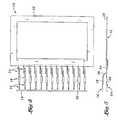
- FIG. 6is a partial cross-sectional view of a memory card constructed in accordance with a second embodiment of the present invention.
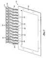
- FIG. 7is a top plan view of the leadframe of the memory card of the second embodiment in a preliminary, unbent state
- FIG. 8is a side-elevational view of a fold-over leadframe constructed in accordance with a third embodiment of the present invention used to mimic the functionality of a CF connector;
- FIG. 9is a side-elevational view of the fold-over leadframe shown in FIG. 8 subsequent to the singulation thereof;
- FIG. 10is a side-elevational view of a fold-over leadframe constructed in accordance with a fourth embodiment of the present invention used to mimic the functionality of a CF connector;
- FIG. 11is a side-elevational view of the fold-over leadframe shown in FIG. 10 subsequent to the singulation thereof;
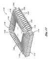
- FIG. 12is a top perspective view of a fold-over leadframe used in a semiconductor package constructed in accordance with a fifth embodiment of the present invention.
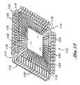
- FIG. 13is a bottom perspective view of the fold-over leadframe shown in FIG. 12 .
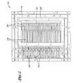
- FIG. 1depicts in cross-section a compact flash (CF) memory card 10 constructed in accordance with a first embodiment of the present invention.
- the memory card 10 of the first embodimentis a “single-sided” version, differing from a “double-sided” version which will be described in more detail below.
- the memory card 10comprises a leadframe 12 which, in an initial unbent state, has a quadrangle shape.
- the leadframe 12comprises a continuous outer frame portion or shorting bar 14 .
- first set of elongate leads 16Integrally connected to and extending inwardly from one common side of the shorting bar 14 is a first set of elongate leads 16 .
- the leads 16 of the first setare arranged in equidistantly spaced relation to each other, and each define an elongate, arcuately contoured coined portion 18 and a land portion 20 .
- the land portions 20 of the leads 16extend to the distal ends thereof.
- each lead 24 of the second setincludes an elongate, arcuately contoured coined portion 26 and a land portion 28 .
- each lead 24 of the second setincludes a bent or angled portion 30 which extends between the coined and the land portions 26 , 28 thereof.
- the distal ends of the leads 24 of the second setare each integrally connected to a cross-bar 32 which is itself integrally connected to and extends perpendicularly between opposed sides of the main frame 22 .
- the leads 24 of the second setare themselves arranged in equidistantly spaced relation to each other. As shown in FIG. 2 , twenty-five leads 16 are included in the first set, with an additional twenty-five leads 24 being included in the second set. In FIGS. 3 and 4 , only thirteen leads 16 , 24 are shown as being included in each of the first and second sets thereof. The reduced number of leads 16 , 24 shown in FIGS.
- the leadframe 12is preferably fabricated from a conductive metallic material such as copper via either a chemical etching or mechanical stamping technique.
- each of the leads 24 of the second setis bent to facilitate the formation of an upwardly angled portion 34 therein.
- the upwardly angled portion 34 of each lead 24is sized and configured so as to result in the top surface of the land portion 28 thereof extending in generally co-planar relation to the top surface of the main frame 22 .
- the leads 16 of the first setare themselves bent so as to each include a downwardly angled portion 36 .
- the downwardly angled portion 36 of each lead 16is sized and configured so as to cause the top surface of the land portion 20 thereof to extend in generally co-planar relation to the top surface of the main frame 22 .
- the leads 16 , 24 of the first and second setsare oriented relative to each other such that the bending or folding over of the leads 24 in the above-described manner coupled with the formation of the upwardly angled portions 34 within the leads 24 and the downwardly angled portions 36 within the leads 16 causes the land portion 28 of each lead 24 to extend in side-by-side, generally parallel relation to the land portion 20 of a respective one of the leads 16 in the manner shown in FIGS. 3-5 .
- the land portions 20 , 28 of the leads 16 , 24are segregated into adjacent pairs, with the top surfaces of the land portions 20 , 28 of each pair being generally co-planar with the top surface of the main frame 22 .
- the coined portions 18 , 26 of the leads 16 , 24are segregated into vertically spaced pairs in the manner also best shown in FIGS. 3 and 5 .
- the formation of the downwardly angled portions 36 within the leads 16causes the coined portions 18 of the leads 16 to be disposed above the coined portions 26 of the leads 24 .
- the coined portions 26 of the leads 24are brought into vertical registry with respective ones of the coined portions 18 due to the inclusion of the angled portions 30 within the leads 24 . As shown in FIG.
- the relative orientations of the leads 16 , 24 subsequent to the bending or folding over of the leads 24results in the cross-bar 32 (which is previously disconnected from the main frame 22 ) extending in vertically spaced, generally parallel relation to that segment of the shorting bar 14 to which the leads 16 are connected.
- the memory card 10comprises a laminate subassembly 38 which is electrically connected to the leadframe 12 subsequent to the bending thereof in a manner which will be described in more detail below.
- the laminate subassembly 38comprises a substrate 40 defining opposed, generally planar top and bottom surfaces. Electrically connected to a common side or surface of the substrate 40 (i.e., the top surface) are one or more electronic components 42 .
- the components) 42may comprise SMT devices and/or passive components. It is contemplated that the substrate 40 will include conductive traces to which the components 42 are electrically connected when mounted to the substrate 40 . As shown in FIG. 1 , certain ones of the components 42 are electrically connected to the conductive traces via conductive wires 44 .
- the conductive tracesare configured to facilitate the routing of signals between the components 42 in a prescribed manner.
- the conductive traceseffectively route the signals to terminal pads 46 which are disposed upon that side or surface of the substrate 40 opposite that including the components 42 mounted thereto (i.e., the bottom surface).
- the terminal pads 46extend along one peripheral edge segment of the substrate 40 , and are arranged in a pattern which allows each of the terminal pads 46 to be brought into direct, electrical contact with a respective one of the land portions 20 , 28 in a manner which will be described in more detail below.
- the laminate subassembly 38 having the above-described structural attributesis electrically connected to the leadframe 12 by positioning the substrate 40 upon the main frame 22 such that the terminal pads 46 are aligned and brought into direct contact with respective ones of the land portions 20 , 28 of the leads 16 , 24 .
- the substrate 40 of the laminate subassembly 38is preferably sized such that it extends along at least portions of the top surfaces of all four peripheral segments of the main frame 22 . As such, the opening defined within the main frame 22 as a result of the bending or folding over of the leads 24 is completely covered by the substrate 40 .
- the profile of the substrate 40is shown by the dashed lines depicted in FIG. 2 .
- the bottom surface of the substrate 40is positioned upon the main frame 22 .
- the substrate 40is preferably affixed to the main frame 22 through the use of an epoxy.
- the top surfaces of the land portions 20 , 28 and/or the terminal pads 46are preferably subjected to a solder paste screening process or solder bumped so that the completion of a reflow process subsequent to the epoxy attachment of the substrate 40 to the main frame 22 will facilitate the electrical connection of each terminal pad 46 of the laminate subassembly 38 to a respective one of the land portions 20 , 28 .
- the leadframe 12is singulated to remove the shorting bar 14 from the main frame 22 and from the leads 16 , with those portions of the leads 16 extending from the coined portions 18 thereof to the shorting bar 14 also being removed as a result of the singulation process.
- the singulation processalso results in the removal of the cross-bar 32 as well as those portions of the leads 24 extending from the coined portions 26 thereof to the cross-bar 32 .
- the remaining portions of the leads 16 , 24are maintained in fixed relation to each other due to the land portions 20 , 28 thereof being electrically connected to and therefore fixed to the laminate subassembly 38 .
- those portions of the leads 24 extending between the upwardly angled portions 34 thereof and the main frame 22are subjected to a cutting operation (e.g., a laser cut) as is needed to facilitate the electrical isolation of the leads 24 from each other. Though such cut effectively separates the leads 24 from the main frame 22 , the leads 24 are maintained in fixed relation to the leads 16 by virtue of their electrical connection to the laminate subassembly 38 as indicated above.
- a cutting operatione.g., a laser cut
- the leadframe 12 and the laminate subassembly 38 electrically connected theretoare at least partially encapsulated with an encapsulant material to facilitate the formation of a package body 48 of the memory card 10 .
- the package body 48is preferably formed or molded in a manner wherein the coined portions 18 , 26 of the leads 16 , 24 extend or protrude into respective slots or cavities defined within the package body 48 .
- the remaining portions of the leads 16 , 24are completely encapsulated by the package body 48 , as is the main frame 22 of the leadframe 12 .
- the package body 48is preferably formed to define another recess or cavity which accommodates the laminate subassembly 38 in a manner wherein the bottom surface of the substrate 40 is covered by the package body 48 , with the top surface of the substrate 40 having the components 42 mounted thereto being uncovered and thus exposed within the cavity.
- the components 42may be protected via the subsequent attachment of a separate lid 50 to the package body 48 , with the lid 50 being sized and configured to cover the cavity formed within the package body 48 to accommodate the laminate subassembly 38 .
- the package body 48could be formed to completely cover or encapsulate the laminate subassembly 38 , thus eliminating the need for the lid 50 .
- the coined portions 18 , 26 exposed within the package body 48mimic the structure and functionality of the fifty pin connector of a conventional CF card.
- the memory card 60 of the second embodimentcomprises the “double-sided” version described above.
- the memory card 60comprises a leadframe 62 which, in an initial unbent state, has a quadrangle shape (i.e., a generally rectangular configuration).
- the leadframe 62comprises an outer frame portion or shorting bar 64 which defines two longitudinally extending sides or segments and two laterally extending sides or segments. Integrally connected to and extending inwardly from one lateral side of the shorting bar 64 is a first set of elongate leads 66 .
- the leads 66 of the first setare arranged in equidistantly spaced relation to each other, and each define an elongate, arcuately contoured coined portion 68 and a land portion 70 .
- the land portions 70 of the leads 68extend to the distal ends thereof.
- a second set of elongate leads 72In addition to the leads 66 of the first set, integrally connected to and extending inwardly from the remaining lateral side of the shorting bar 64 is a second set of elongate leads 72 .
- the leads 72 of the second setare identically configured to the leads 66 of the first set and are arranged in equidistantly spaced relation to each other.
- Each lead 72defines an elongate, arcuately contoured coined portion 74 and a land portion 76 .
- the land portions 76 of the leads 72 of the second setextend to the distal ends thereof.
- first main frame 78 and a second main frame 80attached to the longitudinal sides of the shorting bar 64 and suspended within the interior thereof is a first main frame 78 and a second main frame 80 .
- the first and second main frames 78 , 80each have a generally rectangular configuration.
- the distal ends of the leads 66 of the first setextend toward, but are spaced from, one longitudinal side of the first main frame 78 .
- the distal ends of the leads 72 of the second setextend toward, but are spaced from, one longitudinal side of the second main frame 80 .
- the leadframe 62 of the memory card 60further comprises a pair of connecting bars 84 which are integrally connected to and extend perpendicularly between those longitudinal sides of the first and second main frames 78 , 80 which are disposed adjacent to each other. Extending perpendicularly between the connecting bars 84 is an elongate cross-bar or shorting bar 86 which extends in spaced, generally parallel relation to the longitudinal sides of the first and second main frame 78 , 80 . Integrally connected to the shorting bar 86 are a plurality of leads 88 of a third set which extend perpendicularly relative to the shorting bar 86 toward each of the adjacent longitudinal sides of the first and second main frames 78 , 80 .
- the leads 88 of the third setdo not contact the first and second main frames 78 , 80 , but rather are spaced therefrom at a distance substantially equal to that separating the distal ends of the leads 66 , 72 from respective ones of the longitudinal sides of the first and second main frames 78 , 80 .
- twenty-five leads 66are included in the first set, with twenty-five leads 72 being included in the second set and twenty-five leads 88 being included in the third set.
- the leadframe 62is preferably fabricated from a conductive metallic material such as copper via either a chemical etching or mechanical stamping technique.
- the memory card 60comprises a pair of laminate subassemblies 90 which are each electrically connected to the leadframe 62 in a manner which will be described in more detail below.
- Each laminate subassembly 90comprises a substrate 92 defining opposed, generally planar top and bottom surfaces. Electrically connected to the top surface of each substrate 92 are one or more electronic components 94 .
- the component(s) 94may comprise SMT devices and/or passive components. It is contemplated that each substrate 92 will include conductive traces to which the components 94 are electrically connected when mounted to the corresponding substrate 92 . Certain ones of the components 94 may be electrically connected to the conductive traces via conductive wires 95 .
- each substrate 92are configured to facilitate the routing of signals between the components 94 mounted thereto in a prescribed manner.
- the conductive traceseffectively route the signals to terminal pads 96 which are disposed on the bottom surface of the substrate 92 .
- the terminal pads 96 of each laminate subassembly 90extend along one peripheral edge segment of the substrate 92 thereof, and are arranged in a pattern which allows each of the terminal pads to be brought into direct, electrical contact with respective ones of the land portion 70 of the leads 66 or respective ones of the land portions 76 of the leads 72 in a manner which will be described in more detail below.
- the laminate subassemblies 90are electrically connected to the leadframe 62 by positioning each substrate 92 upon a respective one of the first and second main frames 78 , 80 such that the terminal pads 96 of one laminate subassembly 90 are aligned and brought into direct contact with respective ones of the land portions 70 of the leads 66 , and the terminal pads 96 of the remaining one of the laminate subassemblies 90 are brought into direct contact with respective ones of the land portions 76 of the leads 72 .
- the substrate 92 of each laminate subassembly 90is preferably sized such that it extends along at least portions of the top surfaces of all four peripheral segments of either the first main frame 78 or the second main frame 80 .
- each of the first and second main frames 78 , 80are completely covered by respective ones of the substrates 92 .
- the profile of the substrate 92 of each laminate subassembly 90is depicted by broken lines in FIG. 7 .
- the bottom surfaces of the substrates 92are positioned upon respective ones of the first and second main frames 78 , 80 , with the affixation of the substrates 92 to the first and second main frames 78 , 80 preferably being accomplished through the use of an epoxy.
- the top surfaces of the land portions 70 , 76 and/or the terminal pads 96 of each of the laminate subassemblies 90are preferably subjected to a solder paste screening process or solder bumped so that the completion of a reflow process subsequent to the epoxy attachment of the substrates 92 to the first and second main frames 78 , 80 will facilitate the electrical connection of the terminal pads 96 of one laminate subassembly 90 to respective ones of the land portions 70 , and the electrical connection of the terminal pads 96 of the remaining laminate subassembly 90 to respective ones of the land portions 76 .
- the leadframe 62is singulated to remove the shorting bar 64 from the first and second main frames 78 , 80 and from the leads 66 , 72 . Also removed as a result of the singulation process are those portions of the leads 66 extending between the coined portions 68 and shorting bar 64 , and those portions of the leads 72 extending between the coined portions 74 and the shorting bar 64 .
- the remaining portions of the leads 66are maintained in fixed relation to each other due to the land portions 70 thereof being electrically connected to and therefore fixed to one of the laminate subassemblies 90 .
- the remaining portions of the leads 72are maintained in fixed relation to each other due to the land portions 76 thereof being electrically connected to and therefore fixed to one of the laminate subassemblies 90 .
- the leadframe 62is bent about an axis defined by the shorting bar 86 so as to assume the folded configuration shown in FIG. 6 .
- the original orientations of the leads 66 , 72 as shown in FIG. 7causes the coined portions 68 , 74 thereof to be segregated into twenty-five pairs, with the coined portions 68 , 74 of each pair being in vertically aligned registry with each other.
- the bending or folding of the leadframe 62is completed in a manner wherein the laminate subassemblies 90 are directed outwardly, i.e., are not disposed interiorly between the first and second main frames 78 , 80 of the folded leadframe 62 . It is contemplated that either prior or subsequent to the bending or folding of the leadframe 62 in the above-described manner, those portions of the shorting bar 86 interconnecting the leads 88 of the third set to each other may be removed for purposes of isolating the leads 88 of the third set from each other.
- the leadframe 62 and the laminate subassemblies 90 electrically connected theretoare at least partially encapsulated with an encapsulant material to facilitate the formation of a package body 98 of the memory card 60 .
- the package body 98is preferably formed or molded in a manner wherein the coined portions 68 , 74 of the leads 66 , 72 extend or protrude into respective slots or cavities defined within the package body 98 .
- the remaining portions of the leads 66 , 72are completely encapsulated by the package body 98 , as are the leads 88 of the third set and first and second main frames, 78 , 80 .
- the package body 98is further preferably formed to define an additional pair of recesses or cavities which accommodate respective ones of the laminate subassemblies 90 such that the bottom surfaces of the substrates 92 are covered by the package body 98 , with the top surfaces of the substrates 92 having the components 94 mounted thereto being uncovered and thus exposed within a respective one of the cavities.
- the components 94may be protected via the subsequent attachment of separate lids 100 to the package body 98 , with the lids 100 being sized and configured to cover respective ones of the cavities formed within the package body 98 .
- the package body 98could be formed to completely cover or encapsulate the laminate subassemblies 90 , thus eliminating the need for the lids 100 .
- the coined portions 68 , 74 exposed within the package body 98mimic the structure and functionality of the fifty pin connector of a conventional CF card.
- the leads 88 of the third setcan optionally be used to facilitate the electrical interconnection between the laminate subassemblies 90 .
- conductive wiresmay be used to electrically connect a component 94 of each laminate subassembly 90 to a common lead 88 extending between the first and second main frames 78 , 80 .
- the lead frame 62could be subjected to further cuts as is needed to electrically isolate certain leads 88 of the third set from each other.
- any conductive wires used to facilitate the electrical connection of the laminate subassemblies 90 to one or more of the leads 88would also be encapsulated by the package body 98 .
- solder connectionsmay be employed by outfitting each of the laminate subassemblies 90 with additional terminal pads like the terminal pads 96 described above. Such additional terminal pads of the laminate subassemblies 90 would be used to facilitate the electrical connection thereof to one or more of the leads 88 via soldered connections.
- the memory cards 10 , 60 of the first and second embodimentsdo not include the connector of prior art CF cards in that the coined ends of the leads effectively function as such CF connector.
- the lid component of the prior CF cardsmay be eliminated in the memory card 10 and the memory card 60 , thus also eliminating the separate manufacturing step of attaching the lid to the housing.
- the memory card 10 , 60is significantly more simple in construction than prior art CF cards, and thus significantly less costly to manufacture.
- the laminate subassemblies 90need not necessarily be attached to common sides of the first and second main frames 78 , 80 . If attached to opposite sides of the first and second main frames 78 , 80 , the bending of the leadframe 62 will result in one of the laminate subassemblies 90 being externally presented, with the remaining one of the laminate subassemblies 90 being disposed between the first and second main frames 78 , 80 .
- a leadframe 102which is bent into a clamshell configuration in a manner allowing the same to ultimately serve as a CF connector for a memory card.
- the leadframe 102comprises a plurality of elongate leads 103 which extend in spaced relation to each other and each define a proximal end and an opposed distal end. Formed within each lead 103 between the proximal and distal ends thereof is a spaced pair of coined portions 104 .
- the leadframe 102may be bent such that the proximal and distal ends of each lead 103 are disposed in juxtaposed relation to each other, with the coined portions 104 being disposed in opposed, spaced relation to each other.
- An edge of a substrate 105may be advanced between the juxtaposed proximal and distal ends of the leads 103 , with such proximal and distal ends being electrically connected to corresponding conductive traces on the opposed surfaces of the substrate 105 .
- Such electrical connectionfacilitates the placement of the leads 103 into electrical communication with the substrate 105 in a desired manner.
- mounted (i.e., electrically connected) to the substrate 105are electronic components which are placed into electrical communication with the leads 103 via the conductive traces of the substrate 105 .
- the leadframe 102may alternatively be bent such that the distal end of each lead 103 is separated from a central portion thereof via a narrow gap 106 .
- the coined portions 104 of the leads 103are still disposed in opposed, spaced relation to each other. Thus, only that portion of each lead 103 extending to the proximal end thereof is electrically connected to one side of the substrate 105 .
- the leadframe 102 and substrate 105are encapsulated by a molded housing or package body, with such molded housing subsequently being cut or singulated ( FIGS. 9 and 11 ) in a manner removing a portion of the leadframe 102 as results in the coined portions 104 of the leads 103 defining coined ends which serve as a CF connector.
- an elongate leadframe 112is provided which, in an initial unbent state, has a generally rectangular configuration.
- the strip 112includes a continuous outer frame portion which defines the opposed longitudinal sides and the opposed lateral sides thereof. Disposed within the outer frame portion is a pair of identically configured leadframes 114 of the leadframe strip 112 which are connected to each other in a manner which will be described in more detail below.
- Each leadframe 114 of the leadframe strip 112includes a die pad 116 comprising a substantially square plate which is connected to the outer frame portion by a plurality of tie bars 118 of the leadframe 114 .
- Four tie bars 118are typically used to connect the die pad 116 to the outer frame portion of the strip 112 , with the tie bars 118 extending from respective ones of the four corner regions defined by the die pad 116 .
- Each leadframe 114 of the leadframe strip 112further comprises a multiplicity of leads 120 .
- the leads 120 of each leadframe 114are segregated into four sets, with each set extending toward but being spaced from a respective one of the four peripheral edge segments defined by the die pad 116 .
- the leads 120 of each setare typically equidistantly spaced from each other, with narrow gaps of equal width being defined therebetween.
- One set of the leads 120 of each of the leadframes 114extends to a respective one of the lateral sides defined by the outer frame portion of the strip 112 .
- two sets of the leads 120 of each leadframe 114 disposed in opposed relation to each otherextend to respective ones of the longitudinal sides defined by the outer frame portion of the strip 112 .
- the remaining two sets of leads 120 of the leadframes 114are integrally connected to each other.
- the leads 120 of the integrally connected setsextend to each of the die pads 116 of the strip 112 .
- the center lead 120 of these integrally connected setsextends and is connected to the peripheral edge of each of the die pads 116 .
- the strip 112is preferably fabricated from a copper material, and formed via the completion of an etching or mechanical stamping process.
- the leads 120 of one of the leadframes 114which extend to the lateral and longitudinal sides of the outer frame portion exceed the length of the same leads 120 of the remaining leadframe 114 for reasons which will be discussed in more detail below.
- all of the leads 120 of such leadframe 114are preferably subjected to a half-etching process which is completed in a manner wherein the end portions of the leads 120 disposed furthest from the corresponding die pad 116 are thicker than the remaining portions thereof.
- the formation of the leads 120 of such leadframe 114 to each be of variable thicknessis done for reasons which will also be discussed in more detail below.
- the semiconductor package 110 of the fifth embodimentcomprises a pair of semiconductor dies 122 which are electrically connected to respective ones of the leadframes 114 of the strip 112 .
- Each semiconductor die 122comprises opposed, generally planar top and bottom surfaces, with a plurality of terminal pads being disposed on the top surface thereof.
- the bottom surfaces of the semiconductor dies 122are attached to respective ones of the die pads 116 through the use of an adhesive layer or strip.
- the semiconductor dies 122are attached to common sides of the die pads 116 , and thus are oriented in substantially co-planar relation to each other
- conductive wiresare used to electrically connect the terminal pads of each semiconductor die 122 to respective ones of the leads 120 of the corresponding leadframe 114 .
- Those conductive wires electrically connected to those leads 120 of the leadframes 114 which are integrally connected to each othermay be used to facilitate the electrical communication between the semiconductor dies 122 in a prescribed manner.
- each of the conductive wiresmay be covered or coated with a layer of an encapsulant material to provide mechanical protection to the same.
- laminate subassemblies similar to those described above in relation to the prior embodimentsmay be electrically connected to respective ones of the die pads 116 .
- the terminal pads thereofwould necessarily be oriented so as to allow for the electrical connection thereof to respective ones of the leads 120 through the use of conductive wires.
- the leadframe strip 112is bent into a “clamshell” configuration as shown in FIGS. 12 and 13 .
- the central portions or sections of the leads 120 which are integrally connected to each otherare bent such that the leadframes 114 , and in particular the die pads 116 thereof, extend in juxtaposed relation to each other.
- the leadframe strip 112is preferably bent or folded such that the semiconductor dies 122 reside between the die pads 116 . It will be recognized that the lengths of those leads 120 which are integrally connected to each other must be such that the bending thereof creates a gap between the die pads 116 of the leadframes 114 of sufficient width to accommodate both semiconductor dies 122 .
- the samePrior to the leadframe strip 112 being folded in the above-described manner, the same is preferably subjected to a singulation operation which facilitates the removal of the outer frame portion from the leadframes 114 .
- the completion of the singulation processalso completes the formation of the leads 120 having the differing lengths described above, i.e., those leads 120 of one leadframe 114 other than for the integrally connected leads 120 exceed the lengths of the leads 120 other than for the integrally connected leads 120 of the remaining leadframe 114 .
- Those leads 120 of greater lengthare further subjected to a bending process to impart to the same a generally gull-wing configuration.
- those leads 120 of the leadframe strip 112 of shorter lengthare each half etched such that those end portions disposed furthest from the corresponding die pad 116 are thicker than the remainders thereof.
- the folding or bending of the leadframe strip 112 in the above-described mannerresults in the bottom surfaces of the outwardly flared portions 124 of the bent leads 120 of greater length extending in substantially co-planar relation to the bottom surfaces of the thickened end portions 126 of the leads 120 of shorter length.
- the flared portions 124extend about three sides of the folded leadframe strip 112 , though the thickened portions 126 extend about all four sides thereof.
- the leadframe strip 12After the leadframe strip 12 has been singulated and bent/folded in the above-described manner, the same is partially encapsulated or covered with an encapsulant material which, upon hardening, forms a molded housing or package body.
- the package bodyis formed in a manner wherein the bottom surfaces of the flared portions 124 and the bottom surfaces of the thickened portions 126 are exposed within the bottom surface of the package body and extend in substantially flush or continuous relation therewith.
- the remainder of the leadframe strip 112 and hence the semiconductor dies 122 (or laminate subassemblies)are completely encapsulated by the package body.
- the bottom surface of the die pad 116 toward which the leads 120 of shorter length extendmay be exposed within the bottom surface of the package body, or may alternatively be completely covered thereby.
- the fold-over feature of the leadframe strip 112 of the semiconductor package 110enables higher density since the leads 120 are located directly above each other. Despite this higher density, standard wire bonding processing is used in the fabrication of the semiconductor
Landscapes
- Physics & Mathematics (AREA)
- Condensed Matter Physics & Semiconductors (AREA)
- General Physics & Mathematics (AREA)
- Engineering & Computer Science (AREA)
- Computer Hardware Design (AREA)
- Microelectronics & Electronic Packaging (AREA)
- Power Engineering (AREA)
- Credit Cards Or The Like (AREA)
- Lead Frames For Integrated Circuits (AREA)
Abstract
Description
Claims (22)
Priority Applications (1)
| Application Number | Priority Date | Filing Date | Title |
|---|---|---|---|
| US10/245,071US6919620B1 (en) | 2002-09-17 | 2002-09-17 | Compact flash memory card with clamshell leadframe |
Applications Claiming Priority (1)
| Application Number | Priority Date | Filing Date | Title |
|---|---|---|---|
| US10/245,071US6919620B1 (en) | 2002-09-17 | 2002-09-17 | Compact flash memory card with clamshell leadframe |
Publications (1)
| Publication Number | Publication Date |
|---|---|
| US6919620B1true US6919620B1 (en) | 2005-07-19 |
Family
ID=34738517
Family Applications (1)
| Application Number | Title | Priority Date | Filing Date |
|---|---|---|---|
| US10/245,071Expired - Fee RelatedUS6919620B1 (en) | 2002-09-17 | 2002-09-17 | Compact flash memory card with clamshell leadframe |
Country Status (1)
| Country | Link |
|---|---|
| US (1) | US6919620B1 (en) |
Cited By (4)
| Publication number | Priority date | Publication date | Assignee | Title |
|---|---|---|---|---|
| US20060091543A1 (en)* | 2004-10-28 | 2006-05-04 | Samsung Electronics Co.; Ltd | Land grid array module |
| US20070066139A1 (en)* | 2005-08-31 | 2007-03-22 | Heiko Roeper | Electronic plug unit |
| US20140346658A1 (en)* | 2013-05-21 | 2014-11-27 | International Business Machines Corporation | Fabricating a microelectronics lid using sol-gel processing |
| US20180301401A1 (en)* | 2017-04-12 | 2018-10-18 | Intel Corporation | Multi-level lead frame structures and method of providing same |
Citations (204)
| Publication number | Priority date | Publication date | Assignee | Title |
|---|---|---|---|---|
| US3838984A (en) | 1973-04-16 | 1974-10-01 | Sperry Rand Corp | Flexible carrier and interconnect for uncased ic chips |
| US4054238A (en) | 1976-03-23 | 1977-10-18 | Western Electric Company, Inc. | Method, apparatus and lead frame for assembling leads with terminals on a substrate |
| US4189342A (en) | 1971-10-07 | 1980-02-19 | U.S. Philips Corporation | Semiconductor device comprising projecting contact layers |
| JPS55163868A (en) | 1979-06-08 | 1980-12-20 | Fujitsu Ltd | Lead frame and semiconductor device using the same |
| US4289922A (en) | 1979-09-04 | 1981-09-15 | Plessey Incorporated | Integrated circuit package and lead frame |
| US4301464A (en) | 1978-08-02 | 1981-11-17 | Hitachi, Ltd. | Lead frame and semiconductor device employing the same with improved arrangement of supporting leads for securing the semiconductor supporting member |
| JPS58160095U (en) | 1982-04-21 | 1983-10-25 | アルプス商事株式会社 | car toy |
| US4417266A (en) | 1981-08-14 | 1983-11-22 | Amp Incorporated | Power and ground plane structure for chip carrier |
| JPS59208756A (en) | 1983-05-12 | 1984-11-27 | Sony Corp | Manufacture of semiconductor device package |
| JPS59227143A (en) | 1983-06-07 | 1984-12-20 | Dainippon Printing Co Ltd | Package of integrated circuit |
| US4530152A (en) | 1982-04-01 | 1985-07-23 | Compagnie Industrielle Des Telecommunications Cit-Alcatel | Method for encapsulating semiconductor components using temporary substrates |
| JPS60116239U (en) | 1984-01-12 | 1985-08-06 | 日産自動車株式会社 | Power MOSFET mounting structure |
| JPS60231349A (en) | 1984-05-01 | 1985-11-16 | Toshiba Corp | lead frame |
| JPS60195957U (en) | 1984-06-06 | 1985-12-27 | スズキ株式会社 | Engine intake air temperature automatic adjustment device |
| US4707724A (en) | 1984-06-04 | 1987-11-17 | Hitachi, Ltd. | Semiconductor device and method of manufacturing thereof |
| US4737839A (en) | 1984-03-19 | 1988-04-12 | Trilogy Computer Development Partners, Ltd. | Semiconductor chip mounting system |
| US4756080A (en) | 1986-01-27 | 1988-07-12 | American Microsystems, Inc. | Metal foil semiconductor interconnection method |
| JPS63205935A (en) | 1987-02-23 | 1988-08-25 | Toshiba Corp | Resin-encapsulated semiconductor device with heat sink |
| JPS63233555A (en) | 1987-03-23 | 1988-09-29 | Toshiba Corp | Resin-encapsulated semiconductor device |
| JPS63249345A (en) | 1987-04-06 | 1988-10-17 | Olympus Optical Co Ltd | Flexible mounting substrate |
| JPS63316470A (en) | 1987-06-19 | 1988-12-23 | Alps Electric Co Ltd | Manufacture of thin film transistor |
| US4812896A (en) | 1986-11-13 | 1989-03-14 | Olin Corporation | Metal electronic package sealed with thermoplastic having a grafted metal deactivator and antioxidant |
| JPS6454749U (en) | 1987-09-30 | 1989-04-04 | ||
| US4862245A (en) | 1985-04-18 | 1989-08-29 | International Business Machines Corporation | Package semiconductor chip |
| US4907067A (en) | 1988-05-11 | 1990-03-06 | Texas Instruments Incorporated | Thermally efficient power device package |
| US4920074A (en) | 1987-02-25 | 1990-04-24 | Hitachi, Ltd. | Surface mount plastic package semiconductor integrated circuit, manufacturing method thereof, as well as mounting method and mounted structure thereof |
| US4935803A (en) | 1988-09-09 | 1990-06-19 | Motorola, Inc. | Self-centering electrode for power devices |
| US4987475A (en) | 1988-02-29 | 1991-01-22 | Digital Equipment Corporation | Alignment of leads for ceramic integrated circuit packages |
| US5029386A (en) | 1990-09-17 | 1991-07-09 | Hewlett-Packard Company | Hierarchical tape automated bonding method |
| US5041902A (en) | 1989-12-14 | 1991-08-20 | Motorola, Inc. | Molded electronic package with compression structures |
| US5065223A (en) | 1989-05-31 | 1991-11-12 | Fujitsu Vlsi Limited | Packaged semiconductor device |
| US5070039A (en) | 1989-04-13 | 1991-12-03 | Texas Instruments Incorporated | Method of making an integrated circuit using a pre-served dam bar to reduce mold flash and to facilitate flash removal |
| US5087961A (en) | 1987-01-28 | 1992-02-11 | Lsi Logic Corporation | Semiconductor device package |
| US5096852A (en) | 1988-06-02 | 1992-03-17 | Burr-Brown Corporation | Method of making plastic encapsulated multichip hybrid integrated circuits |
| US5157480A (en) | 1991-02-06 | 1992-10-20 | Motorola, Inc. | Semiconductor device having dual electrical contact sites |
| US5172214A (en) | 1991-02-06 | 1992-12-15 | Motorola, Inc. | Leadless semiconductor device and method for making the same |
| US5172213A (en) | 1991-05-23 | 1992-12-15 | At&T Bell Laboratories | Molded circuit package having heat dissipating post |
| US5200809A (en) | 1991-09-27 | 1993-04-06 | Vlsi Technology, Inc. | Exposed die-attach heatsink package |
| US5200362A (en) | 1989-09-06 | 1993-04-06 | Motorola, Inc. | Method of attaching conductive traces to an encapsulated semiconductor die using a removable transfer film |
| US5214845A (en) | 1992-05-11 | 1993-06-01 | Micron Technology, Inc. | Method for producing high speed integrated circuits |
| US5216278A (en) | 1990-12-04 | 1993-06-01 | Motorola, Inc. | Semiconductor device having a pad array carrier package |
| US5218231A (en) | 1989-08-30 | 1993-06-08 | Kabushiki Kaisha Toshiba | Mold-type semiconductor device |
| US5221642A (en) | 1991-08-15 | 1993-06-22 | Staktek Corporation | Lead-on-chip integrated circuit fabrication method |
| US5250841A (en) | 1992-04-06 | 1993-10-05 | Motorola, Inc. | Semiconductor device with test-only leads |
| US5252853A (en) | 1991-09-19 | 1993-10-12 | Mitsubishi Denki Kabushiki Kaisha | Packaged semiconductor device having tab tape and particular power distribution lead structure |
| US5258094A (en) | 1991-09-18 | 1993-11-02 | Nec Corporation | Method for producing multilayer printed wiring boards |
| US5266834A (en) | 1989-03-13 | 1993-11-30 | Hitachi Ltd. | Semiconductor device and an electronic device with the semiconductor devices mounted thereon |
| US5277972A (en) | 1988-09-29 | 1994-01-11 | Tomoegawa Paper Co., Ltd. | Adhesive tapes |
| US5278446A (en) | 1992-07-06 | 1994-01-11 | Motorola, Inc. | Reduced stress plastic package |
| US5279029A (en) | 1990-08-01 | 1994-01-18 | Staktek Corporation | Ultra high density integrated circuit packages method |
| US5294897A (en) | 1992-07-20 | 1994-03-15 | Mitsubishi Denki Kabushiki Kaisha | Microwave IC package |
| US5327008A (en) | 1993-03-22 | 1994-07-05 | Motorola Inc. | Semiconductor device having universal low-stress die support and method for making the same |
| US5332864A (en) | 1991-12-27 | 1994-07-26 | Vlsi Technology, Inc. | Integrated circuit package having an interposer |
| US5336931A (en) | 1993-09-03 | 1994-08-09 | Motorola, Inc. | Anchoring method for flow formed integrated circuit covers |
| US5335771A (en) | 1990-09-25 | 1994-08-09 | R. H. Murphy Company, Inc. | Spacer trays for stacking storage trays with integrated circuits |
| US5343076A (en) | 1990-07-21 | 1994-08-30 | Mitsui Petrochemical Industries, Ltd. | Semiconductor device with an airtight space formed internally within a hollow package |
| US5391439A (en) | 1990-09-27 | 1995-02-21 | Dai Nippon Printing Co., Ltd. | Leadframe adapted to support semiconductor elements |
| US5406124A (en) | 1992-12-04 | 1995-04-11 | Mitsui Toatsu Chemicals, Inc. | Insulating adhesive tape, and lead frame and semiconductor device employing the tape |
| US5410180A (en) | 1992-07-28 | 1995-04-25 | Shinko Electric Industries Co., Ltd. | Metal plane support for multi-layer lead frames and a process for manufacturing such frames |
| US5414299A (en) | 1993-09-24 | 1995-05-09 | Vlsi Technology, Inc. | Semi-conductor device interconnect package assembly for improved package performance |
| US5428248A (en) | 1992-08-21 | 1995-06-27 | Goldstar Electron Co., Ltd. | Resin molded semiconductor package |
| US5435057A (en) | 1990-10-30 | 1995-07-25 | International Business Machines Corporation | Interconnection method and structure for organic circuit boards |
| US5454905A (en) | 1994-08-09 | 1995-10-03 | National Semiconductor Corporation | Method for manufacturing fine pitch lead frame |
| US5474958A (en) | 1993-05-04 | 1995-12-12 | Motorola, Inc. | Method for making semiconductor device having no die supporting surface |
| US5508556A (en) | 1994-09-02 | 1996-04-16 | Motorola, Inc. | Leaded semiconductor device having accessible power supply pad terminals |
| US5517056A (en) | 1993-09-30 | 1996-05-14 | Motorola, Inc. | Molded carrier ring leadframe having a particular resin injecting area design for gate removal and semiconductor device employing the same |
| US5521429A (en) | 1993-11-25 | 1996-05-28 | Sanyo Electric Co., Ltd. | Surface-mount flat package semiconductor device |
| EP0720234A2 (en) | 1994-12-30 | 1996-07-03 | SILICONIX Incorporated | Vertical power MOSFET having thick metal layer to reduce distributed resistance and method of fabricating the same |
| US5534467A (en) | 1993-03-18 | 1996-07-09 | Lsi Logic Corporation | Semiconductor packages for high I/O semiconductor dies |
| US5539251A (en) | 1992-05-11 | 1996-07-23 | Micron Technology, Inc. | Tie bar over chip lead frame design |
| US5543657A (en) | 1994-10-07 | 1996-08-06 | International Business Machines Corporation | Single layer leadframe design with groundplane capability |
| US5545923A (en) | 1993-10-22 | 1996-08-13 | Lsi Logic Corporation | Semiconductor device assembly with minimized bond finger connections |
| US5544412A (en) | 1994-05-24 | 1996-08-13 | Motorola, Inc. | Method for coupling a power lead to a bond pad in an electronic module |
| US5581122A (en) | 1994-10-25 | 1996-12-03 | Industrial Technology Research Institute | Packaging assembly with consolidated common voltage connections for integrated circuits |
| US5592025A (en) | 1992-08-06 | 1997-01-07 | Motorola, Inc. | Pad array semiconductor device |
| US5594274A (en) | 1993-07-01 | 1997-01-14 | Nec Corporation | Lead frame for use in a semiconductor device and method of manufacturing the semiconductor device using the same |
| US5604376A (en) | 1994-06-30 | 1997-02-18 | Digital Equipment Corporation | Paddleless molded plastic semiconductor chip package |
| US5608267A (en) | 1992-09-17 | 1997-03-04 | Olin Corporation | Molded plastic semiconductor package including heat spreader |
| US5625222A (en) | 1993-11-18 | 1997-04-29 | Fujitsu Limited | Semiconductor device in a resin package housed in a frame having high thermal conductivity |
| US5633528A (en) | 1994-05-25 | 1997-05-27 | Texas Instruments Incorporated | Lead frame structure for IC devices with strengthened encapsulation adhesion |
| US5639990A (en) | 1992-06-05 | 1997-06-17 | Mitsui Toatsu Chemicals, Inc. | Solid printed substrate and electronic circuit package using the same |
| US5640047A (en) | 1995-09-25 | 1997-06-17 | Mitsui High-Tec, Inc. | Ball grid assembly type semiconductor device having a heat diffusion function and an electric and magnetic shielding function |
| US5641997A (en) | 1993-09-14 | 1997-06-24 | Kabushiki Kaisha Toshiba | Plastic-encapsulated semiconductor device |
| US5644169A (en) | 1993-03-04 | 1997-07-01 | Goldstar Electron Co., Ltd. | Mold and method for manufacturing a package for a semiconductor chip and the package manufactured thereby |
| US5646831A (en) | 1995-12-28 | 1997-07-08 | Vlsi Technology, Inc. | Electrically enhanced power quad flat pack arrangement |
| US5650663A (en) | 1995-07-03 | 1997-07-22 | Olin Corporation | Electronic package with improved thermal properties |
| EP0794572A2 (en) | 1996-03-07 | 1997-09-10 | Matsushita Electronics Corporation | Electronic component, method for making the same, and lead frame and mold assembly for use therein |
| US5673479A (en) | 1993-12-20 | 1997-10-07 | Lsi Logic Corporation | Method for mounting a microelectronic circuit peripherally-leaded package including integral support member with spacer |
| US5683806A (en) | 1988-09-29 | 1997-11-04 | Tomoegawa Paper Co., Ltd. | Adhesive tapes |
| US5689135A (en) | 1995-12-19 | 1997-11-18 | Micron Technology, Inc. | Multi-chip device and method of fabrication employing leads over and under processes |
| US5696666A (en) | 1995-10-11 | 1997-12-09 | Motorola, Inc. | Low profile exposed die chip carrier package |
| US5701034A (en) | 1994-05-03 | 1997-12-23 | Amkor Electronics, Inc. | Packaged semiconductor die including heat sink with locking feature |
| US5710064A (en) | 1994-08-16 | 1998-01-20 | Samsung Electronics Co., Ltd. | Method for manufacturing a semiconductor package |
| US5723899A (en) | 1994-08-30 | 1998-03-03 | Amkor Electronics, Inc. | Semiconductor lead frame having connection bar and guide rings |
| US5736432A (en) | 1996-09-20 | 1998-04-07 | National Semiconductor Corporation | Lead frame with lead finger locking feature and method for making same |
| US5745984A (en) | 1995-07-10 | 1998-05-05 | Martin Marietta Corporation | Method for making an electronic module |
| US5770888A (en) | 1995-12-29 | 1998-06-23 | Lg Semicon Co., Ltd. | Integrated chip package with reduced dimensions and leads exposed from the top and bottom of the package |
| US5776798A (en) | 1996-09-04 | 1998-07-07 | Motorola, Inc. | Semiconductor package and method thereof |
| DE19734794A1 (en) | 1997-01-09 | 1998-07-16 | Mitsubishi Electric Corp | Wiring part and lead frame with the wiring part |
| US5783861A (en) | 1994-03-29 | 1998-07-21 | Lg Semicon Co., Ltd. | Semiconductor package and lead frame |
| US5801440A (en) | 1995-10-10 | 1998-09-01 | Acc Microelectronics Corporation | Chip package board having utility rings |
| JPH10256240A (en) | 1997-01-10 | 1998-09-25 | Sony Corp | Manufacture of semiconductor device |
| US5814883A (en) | 1995-10-04 | 1998-09-29 | Mitsubishi Denki Kabushiki Kaisha | Packaged semiconductor chip |
| US5814881A (en) | 1996-12-20 | 1998-09-29 | Lsi Logic Corporation | Stacked integrated chip package and method of making same |
| US5814884A (en) | 1996-10-24 | 1998-09-29 | International Rectifier Corporation | Commonly housed diverse semiconductor die |
| US5817540A (en) | 1996-09-20 | 1998-10-06 | Micron Technology, Inc. | Method of fabricating flip-chip on leads devices and resulting assemblies |
| US5818102A (en)* | 1995-12-29 | 1998-10-06 | Lsi Logic Corporation | System having integrated circuit package with lead frame having internal power and ground busses |
| US5818105A (en) | 1994-07-22 | 1998-10-06 | Nec Corporation | Semiconductor device with plastic material covering a semiconductor chip mounted on a substrate of the device |
| US5821457A (en) | 1994-03-11 | 1998-10-13 | The Panda Project | Semiconductor die carrier having a dielectric epoxy between adjacent leads |
| US5821615A (en) | 1995-12-06 | 1998-10-13 | Lg Semicon Co., Ltd. | Semiconductor chip package having clip-type outlead and fabrication method of same |
| US5835988A (en) | 1996-03-27 | 1998-11-10 | Mitsubishi Denki Kabushiki Kaisha | Packed semiconductor device with wrap around external leads |
| US5844306A (en) | 1995-09-28 | 1998-12-01 | Mitsubishi Denki Kabushiki Kaisha | Die pad structure for solder bonding |
| US5859471A (en) | 1992-11-17 | 1999-01-12 | Shinko Electric Industries Co., Ltd. | Semiconductor device having tab tape lead frame with reinforced outer leads |
| US5866939A (en) | 1996-01-21 | 1999-02-02 | Anam Semiconductor Inc. | Lead end grid array semiconductor package |
| US5874784A (en) | 1995-10-25 | 1999-02-23 | Sharp Kabushiki Kaisha | Semiconductor device having external connection terminals provided on an interconnection plate and fabrication process therefor |
| US5877043A (en) | 1996-02-01 | 1999-03-02 | International Business Machines Corporation | Electronic package with strain relief means and method of making |
| US5886398A (en) | 1997-09-26 | 1999-03-23 | Lsi Logic Corporation | Molded laminate package with integral mold gate |
| US5894108A (en) | 1997-02-11 | 1999-04-13 | National Semiconductor Corporation | Plastic package with exposed die |
| US5897339A (en) | 1996-09-11 | 1999-04-27 | Samsung Electronics Co., Ltd. | Lead-on-chip semiconductor device package having an adhesive layer formed from liquid adhesive and method for manufacturing the same |
| US5900676A (en) | 1996-08-19 | 1999-05-04 | Samsung Electronics Co., Ltd. | Semiconductor device package structure having column leads and a method for production thereof |
| US5903050A (en) | 1998-04-30 | 1999-05-11 | Lsi Logic Corporation | Semiconductor package having capacitive extension spokes and method for making the same |
| US5903049A (en) | 1997-10-29 | 1999-05-11 | Mitsubishi Denki Kabushiki Kaisha | Semiconductor module comprising semiconductor packages |
| US5917242A (en) | 1996-05-20 | 1999-06-29 | Micron Technology, Inc. | Combination of semiconductor interconnect |
| US5939779A (en) | 1996-05-17 | 1999-08-17 | Lg Semicon Co., Ltd. | Bottom lead semiconductor chip stack package |
| US5942794A (en) | 1996-10-22 | 1999-08-24 | Matsushita Electronics Corporation | Plastic encapsulated semiconductor device and method of manufacturing the same |
| US5945731A (en)* | 1995-10-11 | 1999-08-31 | Nec Corporation | Resin encapsulated semiconductor device and method for manufacturing the same |
| KR100220154B1 (en) | 1996-04-01 | 1999-09-01 | 김규현 | Method manufacture of semiconductor package |
| US5951305A (en) | 1998-07-09 | 1999-09-14 | Tessera, Inc. | Lidless socket and method of making same |
| US5959356A (en) | 1995-11-25 | 1999-09-28 | Samsung Electronics Co., Ltd. | Solder ball grid array carrier package with heat sink |
| US5973388A (en) | 1998-01-26 | 1999-10-26 | Motorola, Inc. | Leadframe, method of manufacturing a leadframe, and method of packaging an electronic component utilizing the leadframe |
| US5977630A (en) | 1997-08-15 | 1999-11-02 | International Rectifier Corp. | Plural semiconductor die housed in common package with split heat sink |
| US5977615A (en) | 1996-12-24 | 1999-11-02 | Matsushita Electronics Corporation | Lead frame, method of manufacturing lead frame, semiconductor device and method of manufacturing semiconductor device |
| WO1999056316A1 (en) | 1998-04-28 | 1999-11-04 | Tessera, Inc. | Encapsulation of microelectronic assemblies |
| US5981314A (en) | 1996-10-31 | 1999-11-09 | Amkor Technology, Inc. | Near chip size integrated circuit package |
| US5986333A (en) | 1997-02-27 | 1999-11-16 | Oki Electric Industry Co., Ltd. | Semiconductor apparatus and method for fabricating the same |
| US5986885A (en) | 1997-04-08 | 1999-11-16 | Integrated Device Technology, Inc. | Semiconductor package with internal heatsink and assembly method |
| US6001671A (en) | 1996-04-18 | 1999-12-14 | Tessera, Inc. | Methods for manufacturing a semiconductor package having a sacrificial layer |
| US6013947A (en) | 1997-06-27 | 2000-01-11 | Trimecs Co., Ltd. | Substrate having gate recesses or slots and molding device and molding method thereof |
| US6018189A (en) | 1997-03-31 | 2000-01-25 | Nec Corporation | Lead frame for face-down bonding |
| US6025640A (en) | 1997-07-16 | 2000-02-15 | Dai Nippon Insatsu Kabushiki Kaisha | Resin-sealed semiconductor device, circuit member for use therein and method of manufacturing resin-sealed semiconductor device |
| US6031279A (en) | 1996-09-02 | 2000-02-29 | Siemens Aktiengesellschaft | Power semiconductor component |
| US6034423A (en) | 1998-04-02 | 2000-03-07 | National Semiconductor Corporation | Lead frame design for increased chip pinout |
| USRE36613E (en) | 1993-04-06 | 2000-03-14 | Micron Technology, Inc. | Multi-chip stacked devices |
| US6040626A (en) | 1998-09-25 | 2000-03-21 | International Rectifier Corp. | Semiconductor package |
| US6043430A (en) | 1997-03-14 | 2000-03-28 | Lg Semicon Co., Ltd. | Bottom lead semiconductor chip package |
| US6060768A (en) | 1995-05-09 | 2000-05-09 | Fujitsu Limited | Semiconductor device, method of manufacturing the semiconductor device, and method of manufacturing lead frame |
| US6072228A (en) | 1996-10-25 | 2000-06-06 | Micron Technology, Inc. | Multi-part lead frame with dissimilar materials and method of manufacturing |
| US6075284A (en) | 1998-06-30 | 2000-06-13 | Hyundai Electronics Industries Co., Ltd. | Stack package |
| US6087722A (en) | 1998-05-28 | 2000-07-11 | Samsung Electronics Co., Ltd. | Multi-chip package |
| US6100594A (en) | 1998-01-14 | 2000-08-08 | Sharp Kabushiki Kaisha | Semiconductor device and method of manufacturing the same |
| US6118184A (en) | 1997-07-18 | 2000-09-12 | Sharp Kabushiki Kaisha | Semiconductor device sealed with a sealing resin and including structure to balance sealing resin flow |
| US6118174A (en) | 1996-12-28 | 2000-09-12 | Lg Semicon Co., Ltd. | Bottom lead frame and bottom lead semiconductor package using the same |
| US6130473A (en) | 1998-04-02 | 2000-10-10 | National Semiconductor Corporation | Lead frame chip scale package |
| USRE36907E (en) | 1992-12-07 | 2000-10-10 | Integrated Device Technology, Inc. | Leadframe with power and ground planes |
| US6133623A (en) | 1996-07-03 | 2000-10-17 | Seiko Epson Corporation | Resin sealing type semiconductor device that includes a plurality of leads and method of making the same |
| US6143981A (en) | 1998-06-24 | 2000-11-07 | Amkor Technology, Inc. | Plastic integrated circuit package and method and leadframe for making the package |
| US6169329B1 (en) | 1996-04-02 | 2001-01-02 | Micron Technology, Inc. | Semiconductor devices having interconnections using standardized bonding locations and methods of designing |
| US6177718B1 (en) | 1998-04-28 | 2001-01-23 | Kabushiki Kaisha Toshiba | Resin-sealed semiconductor device |
| US6181002B1 (en) | 1998-12-22 | 2001-01-30 | Sharp Kabushiki Kaisha | Semiconductor device having a plurality of semiconductor chips |
| US6184465B1 (en) | 1998-11-12 | 2001-02-06 | Micron Technology, Inc. | Semiconductor package |
| US6198171B1 (en) | 1999-12-30 | 2001-03-06 | Siliconware Precision Industries Co., Ltd. | Thermally enhanced quad flat non-lead package of semiconductor |
| US6197615B1 (en) | 1997-04-04 | 2001-03-06 | Samsung Electronics Co., Ltd. | Method of producing lead frame having uneven surfaces |
| US6201186B1 (en) | 1998-06-29 | 2001-03-13 | Motorola, Inc. | Electronic component assembly and method of making the same |
| US6201292B1 (en) | 1997-04-02 | 2001-03-13 | Dai Nippon Insatsu Kabushiki Kaisha | Resin-sealed semiconductor device, circuit member used therefor |
| US6204554B1 (en) | 1996-09-05 | 2001-03-20 | International Rectifier Corporation | Surface mount semiconductor package |
| US6208020B1 (en) | 1999-02-24 | 2001-03-27 | Matsushita Electronics Corporation | Leadframe for use in manufacturing a resin-molded semiconductor device |
| US6208023B1 (en) | 1997-07-31 | 2001-03-27 | Matsushita Electronics Corporation | Lead frame for use with an RF powered semiconductor |
| US6211462B1 (en) | 1998-11-05 | 2001-04-03 | Texas Instruments Incorporated | Low inductance power package for integrated circuits |
| US6218731B1 (en) | 1999-05-21 | 2001-04-17 | Siliconware Precision Industries Co., Ltd. | Tiny ball grid array package |
| US6222258B1 (en) | 1996-11-11 | 2001-04-24 | Fujitsu Limited | Semiconductor device and method for producing a semiconductor device |
| US6229200B1 (en) | 1998-06-10 | 2001-05-08 | Asat Limited | Saw-singulated leadless plastic chip carrier |
| US6229205B1 (en) | 1997-06-30 | 2001-05-08 | Samsung Electronics Co., Ltd. | Semiconductor device package having twice-bent tie bar and small die pad |
| US6239384B1 (en) | 1995-09-18 | 2001-05-29 | Tessera, Inc. | Microelectric lead structures with plural conductors |
| US6256200B1 (en) | 1999-05-27 | 2001-07-03 | Allen K. Lam | Symmetrical package for semiconductor die |
| US20010008305A1 (en) | 1998-06-10 | 2001-07-19 | Asat Ltd. | Leadless plastic chip carrier with etch back pad singulation |
| US6282095B1 (en) | 1999-02-02 | 2001-08-28 | Compaq Computer Corporation | Method and system for controlling radio frequency radiation in microelectronic packages using heat dissipation structures |
| US6281566B1 (en) | 1996-09-30 | 2001-08-28 | Sgs-Thomson Microelectronics S.R.L. | Plastic package for electronic devices |
| US6281568B1 (en) | 1998-10-21 | 2001-08-28 | Amkor Technology, Inc. | Plastic integrated circuit device package and leadframe having partially undercut leads and die pad |
| US6285075B1 (en) | 1998-11-02 | 2001-09-04 | Asat, Limited | Integrated circuit package with bonding planes on a ceramic ring using an adhesive assembly |
| US6291273B1 (en) | 1996-12-26 | 2001-09-18 | Hitachi, Ltd. | Plastic molded type semiconductor device and fabrication process thereof |
| US6294100B1 (en) | 1998-06-10 | 2001-09-25 | Asat Ltd | Exposed die leadless plastic chip carrier |
| US6297548B1 (en) | 1998-06-30 | 2001-10-02 | Micron Technology, Inc. | Stackable ceramic FBGA for high thermal applications |
| US6303984B1 (en) | 1997-08-12 | 2001-10-16 | Micron Technology, Inc. | Lead frame including angle iron tie bar |
| US6316838B1 (en) | 1999-10-29 | 2001-11-13 | Fujitsu Limited | Semiconductor device |
| US6323550B1 (en) | 1995-06-06 | 2001-11-27 | Analog Devices, Inc. | Package for sealing an integrated circuit die |
| US6326244B1 (en) | 1998-09-03 | 2001-12-04 | Micron Technology, Inc. | Method of making a cavity ball grid array apparatus |
| US6339255B1 (en) | 1998-10-24 | 2002-01-15 | Hyundai Electronics Industries Co., Ltd. | Stacked semiconductor chips in a single semiconductor package |
| US20020011654A1 (en) | 2000-07-25 | 2002-01-31 | Naoto Kimura | Semiconductor device |
| US20020024122A1 (en) | 2000-08-25 | 2002-02-28 | Samsung Electronics Co., Ltd. | Lead frame having a side ring pad and semiconductor chip package including the same |
| US6353265B1 (en)* | 2001-02-06 | 2002-03-05 | Mitsubishi Denki Kabushiki Kaisha | Semiconductor device |
| US6355502B1 (en) | 2000-04-25 | 2002-03-12 | National Science Council | Semiconductor package and method for making the same |
| US6376283B1 (en) | 2000-04-19 | 2002-04-23 | Power Digital Card Co., Ltd. | Mono-chip multimediacard fabrication method |
| US6380048B1 (en) | 2001-08-02 | 2002-04-30 | St Assembly Test Services Pte Ltd | Die paddle enhancement for exposed pad in semiconductor packaging |
| US6384472B1 (en) | 2000-03-24 | 2002-05-07 | Siliconware Precision Industries Co., Ltd | Leadless image sensor package structure and method for making the same |
| US6395578B1 (en) | 1999-05-20 | 2002-05-28 | Amkor Technology, Inc. | Semiconductor package and method for fabricating the same |
| US6400004B1 (en) | 2000-08-17 | 2002-06-04 | Advanced Semiconductor Engineering, Inc. | Leadless semiconductor package |
| US6444499B1 (en) | 2000-03-30 | 2002-09-03 | Amkor Technology, Inc. | Method for fabricating a snapable multi-package array substrate, snapable multi-package array and snapable packaged electronic components |
| US6452279B2 (en) | 2000-07-14 | 2002-09-17 | Mitsubishi Denki Kabushiki Kaisha | Semiconductor device |
| US20020140061A1 (en) | 2001-03-27 | 2002-10-03 | Lee Hyung Ju | Lead frame for semiconductor package |
| US20020140068A1 (en) | 2001-03-28 | 2002-10-03 | Ming-Hsun Lee | Leadframe-based semiconductor package for multi-media card |
| US6464121B2 (en) | 2000-12-21 | 2002-10-15 | Xerox Corporation | Specialized tool adapted for a process for manufacture and interconnection between adjoining printed wiring boards |
| EP0936671B1 (en) | 1998-02-12 | 2003-05-07 | Hitachi, Ltd. | Resin-moulded semiconductor hybrid module and manufacturing method thereof |
| US6624005B1 (en) | 2000-09-06 | 2003-09-23 | Amkor Technology, Inc. | Semiconductor memory cards and method of making same |
| EP0720225B1 (en) | 1994-12-30 | 2004-10-27 | SILICONIX Incorporated | Lateral power MOSFET having metal strap layer to reduce distributed resistance and method of fabricating the same |
- 2002
- 2002-09-17USUS10/245,071patent/US6919620B1/ennot_activeExpired - Fee Related
Patent Citations (217)
| Publication number | Priority date | Publication date | Assignee | Title |
|---|---|---|---|---|
| US4189342A (en) | 1971-10-07 | 1980-02-19 | U.S. Philips Corporation | Semiconductor device comprising projecting contact layers |
| US3838984A (en) | 1973-04-16 | 1974-10-01 | Sperry Rand Corp | Flexible carrier and interconnect for uncased ic chips |
| US4054238A (en) | 1976-03-23 | 1977-10-18 | Western Electric Company, Inc. | Method, apparatus and lead frame for assembling leads with terminals on a substrate |
| US4301464A (en) | 1978-08-02 | 1981-11-17 | Hitachi, Ltd. | Lead frame and semiconductor device employing the same with improved arrangement of supporting leads for securing the semiconductor supporting member |
| JPS55163868A (en) | 1979-06-08 | 1980-12-20 | Fujitsu Ltd | Lead frame and semiconductor device using the same |
| US4289922A (en) | 1979-09-04 | 1981-09-15 | Plessey Incorporated | Integrated circuit package and lead frame |
| US4417266A (en) | 1981-08-14 | 1983-11-22 | Amp Incorporated | Power and ground plane structure for chip carrier |
| US4530152A (en) | 1982-04-01 | 1985-07-23 | Compagnie Industrielle Des Telecommunications Cit-Alcatel | Method for encapsulating semiconductor components using temporary substrates |
| JPS58160095U (en) | 1982-04-21 | 1983-10-25 | アルプス商事株式会社 | car toy |
| JPS59208756A (en) | 1983-05-12 | 1984-11-27 | Sony Corp | Manufacture of semiconductor device package |
| JPS59227143A (en) | 1983-06-07 | 1984-12-20 | Dainippon Printing Co Ltd | Package of integrated circuit |
| JPS60116239U (en) | 1984-01-12 | 1985-08-06 | 日産自動車株式会社 | Power MOSFET mounting structure |
| US4737839A (en) | 1984-03-19 | 1988-04-12 | Trilogy Computer Development Partners, Ltd. | Semiconductor chip mounting system |
| JPS60231349A (en) | 1984-05-01 | 1985-11-16 | Toshiba Corp | lead frame |
| US4707724A (en) | 1984-06-04 | 1987-11-17 | Hitachi, Ltd. | Semiconductor device and method of manufacturing thereof |
| JPS60195957U (en) | 1984-06-06 | 1985-12-27 | スズキ株式会社 | Engine intake air temperature automatic adjustment device |
| US4862245A (en) | 1985-04-18 | 1989-08-29 | International Business Machines Corporation | Package semiconductor chip |
| US4756080A (en) | 1986-01-27 | 1988-07-12 | American Microsystems, Inc. | Metal foil semiconductor interconnection method |
| US4812896A (en) | 1986-11-13 | 1989-03-14 | Olin Corporation | Metal electronic package sealed with thermoplastic having a grafted metal deactivator and antioxidant |
| US5087961A (en) | 1987-01-28 | 1992-02-11 | Lsi Logic Corporation | Semiconductor device package |
| JPS63205935A (en) | 1987-02-23 | 1988-08-25 | Toshiba Corp | Resin-encapsulated semiconductor device with heat sink |
| US4920074A (en) | 1987-02-25 | 1990-04-24 | Hitachi, Ltd. | Surface mount plastic package semiconductor integrated circuit, manufacturing method thereof, as well as mounting method and mounted structure thereof |
| JPS63233555A (en) | 1987-03-23 | 1988-09-29 | Toshiba Corp | Resin-encapsulated semiconductor device |
| JPS63249345A (en) | 1987-04-06 | 1988-10-17 | Olympus Optical Co Ltd | Flexible mounting substrate |
| JPS63316470A (en) | 1987-06-19 | 1988-12-23 | Alps Electric Co Ltd | Manufacture of thin film transistor |
| JPS6454749U (en) | 1987-09-30 | 1989-04-04 | ||
| US4987475A (en) | 1988-02-29 | 1991-01-22 | Digital Equipment Corporation | Alignment of leads for ceramic integrated circuit packages |
| US4907067A (en) | 1988-05-11 | 1990-03-06 | Texas Instruments Incorporated | Thermally efficient power device package |
| US5096852A (en) | 1988-06-02 | 1992-03-17 | Burr-Brown Corporation | Method of making plastic encapsulated multichip hybrid integrated circuits |
| US4935803A (en) | 1988-09-09 | 1990-06-19 | Motorola, Inc. | Self-centering electrode for power devices |
| US5277972B1 (en) | 1988-09-29 | 1996-11-05 | Tomoegawa Paper Co Ltd | Adhesive tapes |
| US5277972A (en) | 1988-09-29 | 1994-01-11 | Tomoegawa Paper Co., Ltd. | Adhesive tapes |
| US5683806A (en) | 1988-09-29 | 1997-11-04 | Tomoegawa Paper Co., Ltd. | Adhesive tapes |
| US5266834A (en) | 1989-03-13 | 1993-11-30 | Hitachi Ltd. | Semiconductor device and an electronic device with the semiconductor devices mounted thereon |
| US5070039A (en) | 1989-04-13 | 1991-12-03 | Texas Instruments Incorporated | Method of making an integrated circuit using a pre-served dam bar to reduce mold flash and to facilitate flash removal |
| US5065223A (en) | 1989-05-31 | 1991-11-12 | Fujitsu Vlsi Limited | Packaged semiconductor device |
| US5218231A (en) | 1989-08-30 | 1993-06-08 | Kabushiki Kaisha Toshiba | Mold-type semiconductor device |
| US5200362A (en) | 1989-09-06 | 1993-04-06 | Motorola, Inc. | Method of attaching conductive traces to an encapsulated semiconductor die using a removable transfer film |
| US5273938A (en) | 1989-09-06 | 1993-12-28 | Motorola, Inc. | Method for attaching conductive traces to plural, stacked, encapsulated semiconductor die using a removable transfer film |
| US5041902A (en) | 1989-12-14 | 1991-08-20 | Motorola, Inc. | Molded electronic package with compression structures |
| US5343076A (en) | 1990-07-21 | 1994-08-30 | Mitsui Petrochemical Industries, Ltd. | Semiconductor device with an airtight space formed internally within a hollow package |
| US5279029A (en) | 1990-08-01 | 1994-01-18 | Staktek Corporation | Ultra high density integrated circuit packages method |
| US5029386A (en) | 1990-09-17 | 1991-07-09 | Hewlett-Packard Company | Hierarchical tape automated bonding method |
| US5335771A (en) | 1990-09-25 | 1994-08-09 | R. H. Murphy Company, Inc. | Spacer trays for stacking storage trays with integrated circuits |
| US5391439A (en) | 1990-09-27 | 1995-02-21 | Dai Nippon Printing Co., Ltd. | Leadframe adapted to support semiconductor elements |
| US5435057A (en) | 1990-10-30 | 1995-07-25 | International Business Machines Corporation | Interconnection method and structure for organic circuit boards |
| US5216278A (en) | 1990-12-04 | 1993-06-01 | Motorola, Inc. | Semiconductor device having a pad array carrier package |
| US5157480A (en) | 1991-02-06 | 1992-10-20 | Motorola, Inc. | Semiconductor device having dual electrical contact sites |
| US5172214A (en) | 1991-02-06 | 1992-12-15 | Motorola, Inc. | Leadless semiconductor device and method for making the same |
| US5172213A (en) | 1991-05-23 | 1992-12-15 | At&T Bell Laboratories | Molded circuit package having heat dissipating post |
| US5221642A (en) | 1991-08-15 | 1993-06-22 | Staktek Corporation | Lead-on-chip integrated circuit fabrication method |
| US5258094A (en) | 1991-09-18 | 1993-11-02 | Nec Corporation | Method for producing multilayer printed wiring boards |
| US5252853A (en) | 1991-09-19 | 1993-10-12 | Mitsubishi Denki Kabushiki Kaisha | Packaged semiconductor device having tab tape and particular power distribution lead structure |
| US5200809A (en) | 1991-09-27 | 1993-04-06 | Vlsi Technology, Inc. | Exposed die-attach heatsink package |
| US5332864A (en) | 1991-12-27 | 1994-07-26 | Vlsi Technology, Inc. | Integrated circuit package having an interposer |
| US5250841A (en) | 1992-04-06 | 1993-10-05 | Motorola, Inc. | Semiconductor device with test-only leads |
| US5539251A (en) | 1992-05-11 | 1996-07-23 | Micron Technology, Inc. | Tie bar over chip lead frame design |
| US5214845A (en) | 1992-05-11 | 1993-06-01 | Micron Technology, Inc. | Method for producing high speed integrated circuits |
| US5639990A (en) | 1992-06-05 | 1997-06-17 | Mitsui Toatsu Chemicals, Inc. | Solid printed substrate and electronic circuit package using the same |
| US5278446A (en) | 1992-07-06 | 1994-01-11 | Motorola, Inc. | Reduced stress plastic package |
| US5294897A (en) | 1992-07-20 | 1994-03-15 | Mitsubishi Denki Kabushiki Kaisha | Microwave IC package |
| US5410180A (en) | 1992-07-28 | 1995-04-25 | Shinko Electric Industries Co., Ltd. | Metal plane support for multi-layer lead frames and a process for manufacturing such frames |
| US5592025A (en) | 1992-08-06 | 1997-01-07 | Motorola, Inc. | Pad array semiconductor device |
| US5428248A (en) | 1992-08-21 | 1995-06-27 | Goldstar Electron Co., Ltd. | Resin molded semiconductor package |
| US5608267A (en) | 1992-09-17 | 1997-03-04 | Olin Corporation | Molded plastic semiconductor package including heat spreader |
| US5859471A (en) | 1992-11-17 | 1999-01-12 | Shinko Electric Industries Co., Ltd. | Semiconductor device having tab tape lead frame with reinforced outer leads |
| US5406124A (en) | 1992-12-04 | 1995-04-11 | Mitsui Toatsu Chemicals, Inc. | Insulating adhesive tape, and lead frame and semiconductor device employing the tape |
| USRE36907E (en) | 1992-12-07 | 2000-10-10 | Integrated Device Technology, Inc. | Leadframe with power and ground planes |
| US5644169A (en) | 1993-03-04 | 1997-07-01 | Goldstar Electron Co., Ltd. | Mold and method for manufacturing a package for a semiconductor chip and the package manufactured thereby |
| US5534467A (en) | 1993-03-18 | 1996-07-09 | Lsi Logic Corporation | Semiconductor packages for high I/O semiconductor dies |
| US5424576A (en) | 1993-03-22 | 1995-06-13 | Motorola, Inc. | Semiconductor device having x-shaped die support member and method for making the same |
| US5327008A (en) | 1993-03-22 | 1994-07-05 | Motorola Inc. | Semiconductor device having universal low-stress die support and method for making the same |
| USRE36613E (en) | 1993-04-06 | 2000-03-14 | Micron Technology, Inc. | Multi-chip stacked devices |
| US5474958A (en) | 1993-05-04 | 1995-12-12 | Motorola, Inc. | Method for making semiconductor device having no die supporting surface |
| US5594274A (en) | 1993-07-01 | 1997-01-14 | Nec Corporation | Lead frame for use in a semiconductor device and method of manufacturing the semiconductor device using the same |
| US5336931A (en) | 1993-09-03 | 1994-08-09 | Motorola, Inc. | Anchoring method for flow formed integrated circuit covers |
| US5641997A (en) | 1993-09-14 | 1997-06-24 | Kabushiki Kaisha Toshiba | Plastic-encapsulated semiconductor device |
| US5414299A (en) | 1993-09-24 | 1995-05-09 | Vlsi Technology, Inc. | Semi-conductor device interconnect package assembly for improved package performance |
| US5517056A (en) | 1993-09-30 | 1996-05-14 | Motorola, Inc. | Molded carrier ring leadframe having a particular resin injecting area design for gate removal and semiconductor device employing the same |
| US5545923A (en) | 1993-10-22 | 1996-08-13 | Lsi Logic Corporation | Semiconductor device assembly with minimized bond finger connections |
| US5625222A (en) | 1993-11-18 | 1997-04-29 | Fujitsu Limited | Semiconductor device in a resin package housed in a frame having high thermal conductivity |
| US5521429A (en) | 1993-11-25 | 1996-05-28 | Sanyo Electric Co., Ltd. | Surface-mount flat package semiconductor device |
| US5673479A (en) | 1993-12-20 | 1997-10-07 | Lsi Logic Corporation | Method for mounting a microelectronic circuit peripherally-leaded package including integral support member with spacer |
| US5821457A (en) | 1994-03-11 | 1998-10-13 | The Panda Project | Semiconductor die carrier having a dielectric epoxy between adjacent leads |
| US5783861A (en) | 1994-03-29 | 1998-07-21 | Lg Semicon Co., Ltd. | Semiconductor package and lead frame |
| US5701034A (en) | 1994-05-03 | 1997-12-23 | Amkor Electronics, Inc. | Packaged semiconductor die including heat sink with locking feature |
| US5544412A (en) | 1994-05-24 | 1996-08-13 | Motorola, Inc. | Method for coupling a power lead to a bond pad in an electronic module |
| US5633528A (en) | 1994-05-25 | 1997-05-27 | Texas Instruments Incorporated | Lead frame structure for IC devices with strengthened encapsulation adhesion |
| US5604376A (en) | 1994-06-30 | 1997-02-18 | Digital Equipment Corporation | Paddleless molded plastic semiconductor chip package |
| US5818105A (en) | 1994-07-22 | 1998-10-06 | Nec Corporation | Semiconductor device with plastic material covering a semiconductor chip mounted on a substrate of the device |
| US5454905A (en) | 1994-08-09 | 1995-10-03 | National Semiconductor Corporation | Method for manufacturing fine pitch lead frame |
| US5710064A (en) | 1994-08-16 | 1998-01-20 | Samsung Electronics Co., Ltd. | Method for manufacturing a semiconductor package |
| US5723899A (en) | 1994-08-30 | 1998-03-03 | Amkor Electronics, Inc. | Semiconductor lead frame having connection bar and guide rings |
| US5508556A (en) | 1994-09-02 | 1996-04-16 | Motorola, Inc. | Leaded semiconductor device having accessible power supply pad terminals |
| US5814877A (en) | 1994-10-07 | 1998-09-29 | International Business Machines Corporation | Single layer leadframe design with groundplane capability |
| US5543657A (en) | 1994-10-07 | 1996-08-06 | International Business Machines Corporation | Single layer leadframe design with groundplane capability |
| US5581122A (en) | 1994-10-25 | 1996-12-03 | Industrial Technology Research Institute | Packaging assembly with consolidated common voltage connections for integrated circuits |
| EP0720234A2 (en) | 1994-12-30 | 1996-07-03 | SILICONIX Incorporated | Vertical power MOSFET having thick metal layer to reduce distributed resistance and method of fabricating the same |
| EP0720225B1 (en) | 1994-12-30 | 2004-10-27 | SILICONIX Incorporated | Lateral power MOSFET having metal strap layer to reduce distributed resistance and method of fabricating the same |
| US5665996A (en) | 1994-12-30 | 1997-09-09 | Siliconix Incorporated | Vertical power mosfet having thick metal layer to reduce distributed resistance |
| US6060768A (en) | 1995-05-09 | 2000-05-09 | Fujitsu Limited | Semiconductor device, method of manufacturing the semiconductor device, and method of manufacturing lead frame |
| US6323550B1 (en) | 1995-06-06 | 2001-11-27 | Analog Devices, Inc. | Package for sealing an integrated circuit die |
| US5650663A (en) | 1995-07-03 | 1997-07-22 | Olin Corporation | Electronic package with improved thermal properties |
| US5745984A (en) | 1995-07-10 | 1998-05-05 | Martin Marietta Corporation | Method for making an electronic module |
| US6239384B1 (en) | 1995-09-18 | 2001-05-29 | Tessera, Inc. | Microelectric lead structures with plural conductors |
| US5640047A (en) | 1995-09-25 | 1997-06-17 | Mitsui High-Tec, Inc. | Ball grid assembly type semiconductor device having a heat diffusion function and an electric and magnetic shielding function |
| US5844306A (en) | 1995-09-28 | 1998-12-01 | Mitsubishi Denki Kabushiki Kaisha | Die pad structure for solder bonding |
| US5814883A (en) | 1995-10-04 | 1998-09-29 | Mitsubishi Denki Kabushiki Kaisha | Packaged semiconductor chip |
| US5801440A (en) | 1995-10-10 | 1998-09-01 | Acc Microelectronics Corporation | Chip package board having utility rings |
| US5696666A (en) | 1995-10-11 | 1997-12-09 | Motorola, Inc. | Low profile exposed die chip carrier package |
| US5945731A (en)* | 1995-10-11 | 1999-08-31 | Nec Corporation | Resin encapsulated semiconductor device and method for manufacturing the same |
| US5874784A (en) | 1995-10-25 | 1999-02-23 | Sharp Kabushiki Kaisha | Semiconductor device having external connection terminals provided on an interconnection plate and fabrication process therefor |
| US5959356A (en) | 1995-11-25 | 1999-09-28 | Samsung Electronics Co., Ltd. | Solder ball grid array carrier package with heat sink |
| US5821615A (en) | 1995-12-06 | 1998-10-13 | Lg Semicon Co., Ltd. | Semiconductor chip package having clip-type outlead and fabrication method of same |
| US5689135A (en) | 1995-12-19 | 1997-11-18 | Micron Technology, Inc. | Multi-chip device and method of fabrication employing leads over and under processes |
| US5646831A (en) | 1995-12-28 | 1997-07-08 | Vlsi Technology, Inc. | Electrically enhanced power quad flat pack arrangement |
| US5818102A (en)* | 1995-12-29 | 1998-10-06 | Lsi Logic Corporation | System having integrated circuit package with lead frame having internal power and ground busses |
| US5770888A (en) | 1995-12-29 | 1998-06-23 | Lg Semicon Co., Ltd. | Integrated chip package with reduced dimensions and leads exposed from the top and bottom of the package |
| US5866939A (en) | 1996-01-21 | 1999-02-02 | Anam Semiconductor Inc. | Lead end grid array semiconductor package |
| US5877043A (en) | 1996-02-01 | 1999-03-02 | International Business Machines Corporation | Electronic package with strain relief means and method of making |
| EP0794572A2 (en) | 1996-03-07 | 1997-09-10 | Matsushita Electronics Corporation | Electronic component, method for making the same, and lead frame and mold assembly for use therein |
| US5977613A (en) | 1996-03-07 | 1999-11-02 | Matsushita Electronics Corporation | Electronic component, method for making the same, and lead frame and mold assembly for use therein |
| US5835988A (en) | 1996-03-27 | 1998-11-10 | Mitsubishi Denki Kabushiki Kaisha | Packed semiconductor device with wrap around external leads |
| KR100220154B1 (en) | 1996-04-01 | 1999-09-01 | 김규현 | Method manufacture of semiconductor package |
| US6169329B1 (en) | 1996-04-02 | 2001-01-02 | Micron Technology, Inc. | Semiconductor devices having interconnections using standardized bonding locations and methods of designing |
| US6294830B1 (en) | 1996-04-18 | 2001-09-25 | Tessera, Inc. | Microelectronic assembly with conductive terminals having an exposed surface through a dielectric layer |
| US6001671A (en) | 1996-04-18 | 1999-12-14 | Tessera, Inc. | Methods for manufacturing a semiconductor package having a sacrificial layer |
| US5939779A (en) | 1996-05-17 | 1999-08-17 | Lg Semicon Co., Ltd. | Bottom lead semiconductor chip stack package |
| US5917242A (en) | 1996-05-20 | 1999-06-29 | Micron Technology, Inc. | Combination of semiconductor interconnect |
| US6133623A (en) | 1996-07-03 | 2000-10-17 | Seiko Epson Corporation | Resin sealing type semiconductor device that includes a plurality of leads and method of making the same |
| US5900676A (en) | 1996-08-19 | 1999-05-04 | Samsung Electronics Co., Ltd. | Semiconductor device package structure having column leads and a method for production thereof |
| US6031279A (en) | 1996-09-02 | 2000-02-29 | Siemens Aktiengesellschaft | Power semiconductor component |
| US5776798A (en) | 1996-09-04 | 1998-07-07 | Motorola, Inc. | Semiconductor package and method thereof |
| US6204554B1 (en) | 1996-09-05 | 2001-03-20 | International Rectifier Corporation | Surface mount semiconductor package |
| US5897339A (en) | 1996-09-11 | 1999-04-27 | Samsung Electronics Co., Ltd. | Lead-on-chip semiconductor device package having an adhesive layer formed from liquid adhesive and method for manufacturing the same |
| US5817540A (en) | 1996-09-20 | 1998-10-06 | Micron Technology, Inc. | Method of fabricating flip-chip on leads devices and resulting assemblies |
| US6060769A (en) | 1996-09-20 | 2000-05-09 | Micron Technology, Inc. | Flip-chip on leads devices |
| US5736432A (en) | 1996-09-20 | 1998-04-07 | National Semiconductor Corporation | Lead frame with lead finger locking feature and method for making same |
| US6281566B1 (en) | 1996-09-30 | 2001-08-28 | Sgs-Thomson Microelectronics S.R.L. | Plastic package for electronic devices |
| US6130115A (en) | 1996-10-22 | 2000-10-10 | Matsushita Electronics Corporation | Plastic encapsulated semiconductor device and method of manufacturing the same |
| US5942794A (en) | 1996-10-22 | 1999-08-24 | Matsushita Electronics Corporation | Plastic encapsulated semiconductor device and method of manufacturing the same |
| US5814884A (en) | 1996-10-24 | 1998-09-29 | International Rectifier Corporation | Commonly housed diverse semiconductor die |
| US5814884C1 (en) | 1996-10-24 | 2002-01-29 | Int Rectifier Corp | Commonly housed diverse semiconductor die |
| US6072228A (en) | 1996-10-25 | 2000-06-06 | Micron Technology, Inc. | Multi-part lead frame with dissimilar materials and method of manufacturing |
| US6140154A (en) | 1996-10-25 | 2000-10-31 | Micron Technology, Inc. | Multi-part lead frame with dissimilar materials and method of manufacturing |
| US5981314A (en) | 1996-10-31 | 1999-11-09 | Amkor Technology, Inc. | Near chip size integrated circuit package |
| US6222258B1 (en) | 1996-11-11 | 2001-04-24 | Fujitsu Limited | Semiconductor device and method for producing a semiconductor device |
| US5814881A (en) | 1996-12-20 | 1998-09-29 | Lsi Logic Corporation | Stacked integrated chip package and method of making same |
| US6225146B1 (en) | 1996-12-24 | 2001-05-01 | Matsushita Electronics Corporation | Lead frame, method of manufacturing lead frame, semiconductor device and method of manufacturing semiconductor device |
| US5977615A (en) | 1996-12-24 | 1999-11-02 | Matsushita Electronics Corporation | Lead frame, method of manufacturing lead frame, semiconductor device and method of manufacturing semiconductor device |
| US6291273B1 (en) | 1996-12-26 | 2001-09-18 | Hitachi, Ltd. | Plastic molded type semiconductor device and fabrication process thereof |
| US6118174A (en) | 1996-12-28 | 2000-09-12 | Lg Semicon Co., Ltd. | Bottom lead frame and bottom lead semiconductor package using the same |
| DE19734794A1 (en) | 1997-01-09 | 1998-07-16 | Mitsubishi Electric Corp | Wiring part and lead frame with the wiring part |
| JPH10256240A (en) | 1997-01-10 | 1998-09-25 | Sony Corp | Manufacture of semiconductor device |
| US5894108A (en) | 1997-02-11 | 1999-04-13 | National Semiconductor Corporation | Plastic package with exposed die |
| US5986333A (en) | 1997-02-27 | 1999-11-16 | Oki Electric Industry Co., Ltd. | Semiconductor apparatus and method for fabricating the same |
| US6043430A (en) | 1997-03-14 | 2000-03-28 | Lg Semicon Co., Ltd. | Bottom lead semiconductor chip package |
| US6018189A (en) | 1997-03-31 | 2000-01-25 | Nec Corporation | Lead frame for face-down bonding |
| US6201292B1 (en) | 1997-04-02 | 2001-03-13 | Dai Nippon Insatsu Kabushiki Kaisha | Resin-sealed semiconductor device, circuit member used therefor |
| US6197615B1 (en) | 1997-04-04 | 2001-03-06 | Samsung Electronics Co., Ltd. | Method of producing lead frame having uneven surfaces |
| US5986885A (en) | 1997-04-08 | 1999-11-16 | Integrated Device Technology, Inc. | Semiconductor package with internal heatsink and assembly method |
| US6013947A (en) | 1997-06-27 | 2000-01-11 | Trimecs Co., Ltd. | Substrate having gate recesses or slots and molding device and molding method thereof |
| US6229205B1 (en) | 1997-06-30 | 2001-05-08 | Samsung Electronics Co., Ltd. | Semiconductor device package having twice-bent tie bar and small die pad |
| US6025640A (en) | 1997-07-16 | 2000-02-15 | Dai Nippon Insatsu Kabushiki Kaisha | Resin-sealed semiconductor device, circuit member for use therein and method of manufacturing resin-sealed semiconductor device |
| US6118184A (en) | 1997-07-18 | 2000-09-12 | Sharp Kabushiki Kaisha | Semiconductor device sealed with a sealing resin and including structure to balance sealing resin flow |
| US6208023B1 (en) | 1997-07-31 | 2001-03-27 | Matsushita Electronics Corporation | Lead frame for use with an RF powered semiconductor |
| US6303984B1 (en) | 1997-08-12 | 2001-10-16 | Micron Technology, Inc. | Lead frame including angle iron tie bar |
| US5977630A (en) | 1997-08-15 | 1999-11-02 | International Rectifier Corp. | Plural semiconductor die housed in common package with split heat sink |
| US5886398A (en) | 1997-09-26 | 1999-03-23 | Lsi Logic Corporation | Molded laminate package with integral mold gate |
| US5903049A (en) | 1997-10-29 | 1999-05-11 | Mitsubishi Denki Kabushiki Kaisha | Semiconductor module comprising semiconductor packages |
| US6100594A (en) | 1998-01-14 | 2000-08-08 | Sharp Kabushiki Kaisha | Semiconductor device and method of manufacturing the same |
| US5973388A (en) | 1998-01-26 | 1999-10-26 | Motorola, Inc. | Leadframe, method of manufacturing a leadframe, and method of packaging an electronic component utilizing the leadframe |
| EP0936671B1 (en) | 1998-02-12 | 2003-05-07 | Hitachi, Ltd. | Resin-moulded semiconductor hybrid module and manufacturing method thereof |
| US6130473A (en) | 1998-04-02 | 2000-10-10 | National Semiconductor Corporation | Lead frame chip scale package |
| US6034423A (en) | 1998-04-02 | 2000-03-07 | National Semiconductor Corporation | Lead frame design for increased chip pinout |
| US6177718B1 (en) | 1998-04-28 | 2001-01-23 | Kabushiki Kaisha Toshiba | Resin-sealed semiconductor device |
| WO1999056316A1 (en) | 1998-04-28 | 1999-11-04 | Tessera, Inc. | Encapsulation of microelectronic assemblies |
| US5903050A (en) | 1998-04-30 | 1999-05-11 | Lsi Logic Corporation | Semiconductor package having capacitive extension spokes and method for making the same |
| US6087722A (en) | 1998-05-28 | 2000-07-11 | Samsung Electronics Co., Ltd. | Multi-chip package |
| US6229200B1 (en) | 1998-06-10 | 2001-05-08 | Asat Limited | Saw-singulated leadless plastic chip carrier |
| US6242281B1 (en) | 1998-06-10 | 2001-06-05 | Asat, Limited | Saw-singulated leadless plastic chip carrier |
| US6294100B1 (en) | 1998-06-10 | 2001-09-25 | Asat Ltd | Exposed die leadless plastic chip carrier |
| US20010008305A1 (en) | 1998-06-10 | 2001-07-19 | Asat Ltd. | Leadless plastic chip carrier with etch back pad singulation |
| US6143981A (en) | 1998-06-24 | 2000-11-07 | Amkor Technology, Inc. | Plastic integrated circuit package and method and leadframe for making the package |
| US6201186B1 (en) | 1998-06-29 | 2001-03-13 | Motorola, Inc. | Electronic component assembly and method of making the same |
| US6075284A (en) | 1998-06-30 | 2000-06-13 | Hyundai Electronics Industries Co., Ltd. | Stack package |
| US6297548B1 (en) | 1998-06-30 | 2001-10-02 | Micron Technology, Inc. | Stackable ceramic FBGA for high thermal applications |
| US5951305A (en) | 1998-07-09 | 1999-09-14 | Tessera, Inc. | Lidless socket and method of making same |
| US6326244B1 (en) | 1998-09-03 | 2001-12-04 | Micron Technology, Inc. | Method of making a cavity ball grid array apparatus |
| US6040626A (en) | 1998-09-25 | 2000-03-21 | International Rectifier Corp. | Semiconductor package |
| US6281568B1 (en) | 1998-10-21 | 2001-08-28 | Amkor Technology, Inc. | Plastic integrated circuit device package and leadframe having partially undercut leads and die pad |
| US6339255B1 (en) | 1998-10-24 | 2002-01-15 | Hyundai Electronics Industries Co., Ltd. | Stacked semiconductor chips in a single semiconductor package |
| US6285075B1 (en) | 1998-11-02 | 2001-09-04 | Asat, Limited | Integrated circuit package with bonding planes on a ceramic ring using an adhesive assembly |
| US6211462B1 (en) | 1998-11-05 | 2001-04-03 | Texas Instruments Incorporated | Low inductance power package for integrated circuits |
| US6184465B1 (en) | 1998-11-12 | 2001-02-06 | Micron Technology, Inc. | Semiconductor package |
| US6181002B1 (en) | 1998-12-22 | 2001-01-30 | Sharp Kabushiki Kaisha | Semiconductor device having a plurality of semiconductor chips |
| US6282095B1 (en) | 1999-02-02 | 2001-08-28 | Compaq Computer Corporation | Method and system for controlling radio frequency radiation in microelectronic packages using heat dissipation structures |
| US6208020B1 (en) | 1999-02-24 | 2001-03-27 | Matsushita Electronics Corporation | Leadframe for use in manufacturing a resin-molded semiconductor device |
| US6395578B1 (en) | 1999-05-20 | 2002-05-28 | Amkor Technology, Inc. | Semiconductor package and method for fabricating the same |
| US6218731B1 (en) | 1999-05-21 | 2001-04-17 | Siliconware Precision Industries Co., Ltd. | Tiny ball grid array package |
| US6256200B1 (en) | 1999-05-27 | 2001-07-03 | Allen K. Lam | Symmetrical package for semiconductor die |
| US6316838B1 (en) | 1999-10-29 | 2001-11-13 | Fujitsu Limited | Semiconductor device |
| US6198171B1 (en) | 1999-12-30 | 2001-03-06 | Siliconware Precision Industries Co., Ltd. | Thermally enhanced quad flat non-lead package of semiconductor |
| US6384472B1 (en) | 2000-03-24 | 2002-05-07 | Siliconware Precision Industries Co., Ltd | Leadless image sensor package structure and method for making the same |
| US6444499B1 (en) | 2000-03-30 | 2002-09-03 | Amkor Technology, Inc. | Method for fabricating a snapable multi-package array substrate, snapable multi-package array and snapable packaged electronic components |
| US6376283B1 (en) | 2000-04-19 | 2002-04-23 | Power Digital Card Co., Ltd. | Mono-chip multimediacard fabrication method |
| US6355502B1 (en) | 2000-04-25 | 2002-03-12 | National Science Council | Semiconductor package and method for making the same |
| US6452279B2 (en) | 2000-07-14 | 2002-09-17 | Mitsubishi Denki Kabushiki Kaisha | Semiconductor device |
| US20020011654A1 (en) | 2000-07-25 | 2002-01-31 | Naoto Kimura | Semiconductor device |
| US6400004B1 (en) | 2000-08-17 | 2002-06-04 | Advanced Semiconductor Engineering, Inc. | Leadless semiconductor package |
| US20020024122A1 (en) | 2000-08-25 | 2002-02-28 | Samsung Electronics Co., Ltd. | Lead frame having a side ring pad and semiconductor chip package including the same |
| US6624005B1 (en) | 2000-09-06 | 2003-09-23 | Amkor Technology, Inc. | Semiconductor memory cards and method of making same |
| US6464121B2 (en) | 2000-12-21 | 2002-10-15 | Xerox Corporation | Specialized tool adapted for a process for manufacture and interconnection between adjoining printed wiring boards |
| US6353265B1 (en)* | 2001-02-06 | 2002-03-05 | Mitsubishi Denki Kabushiki Kaisha | Semiconductor device |
| US20020140061A1 (en) | 2001-03-27 | 2002-10-03 | Lee Hyung Ju | Lead frame for semiconductor package |
| US20020140068A1 (en) | 2001-03-28 | 2002-10-03 | Ming-Hsun Lee | Leadframe-based semiconductor package for multi-media card |
| US6380048B1 (en) | 2001-08-02 | 2002-04-30 | St Assembly Test Services Pte Ltd | Die paddle enhancement for exposed pad in semiconductor packaging |
Non-Patent Citations (4)
| Title |
|---|
| JEDEC Solid State Product Outline, "2 Lead Header Family Surface Mounted (Peripheral Terminals)", 4 pages. |
| Mannion, P., "MOSFETs Break Out of the Shackles of Wirebonding", Electronic Design, vol. 47, #6 (Mar. 22, 1999). |
| Micro Electronics Packaging Handbook, 1989, edited by R. Tummala & E. Rymaszewski, published by Van Nostrand Reinhold. NewYork, NY. |
| Vishay Siliconix Press Release, http://www.siliconix.com/www/200/pr98/4430.html, Dec. 9, 1998, pp. 1-3. |
Cited By (6)
| Publication number | Priority date | Publication date | Assignee | Title |
|---|---|---|---|---|
| US20060091543A1 (en)* | 2004-10-28 | 2006-05-04 | Samsung Electronics Co.; Ltd | Land grid array module |
| US7208824B2 (en)* | 2004-10-28 | 2007-04-24 | Samsung Electronics Co., Ltd. | Land grid array module |
| US20070066139A1 (en)* | 2005-08-31 | 2007-03-22 | Heiko Roeper | Electronic plug unit |
| US20140346658A1 (en)* | 2013-05-21 | 2014-11-27 | International Business Machines Corporation | Fabricating a microelectronics lid using sol-gel processing |
| US9478473B2 (en)* | 2013-05-21 | 2016-10-25 | Globalfoundries Inc. | Fabricating a microelectronics lid using sol-gel processing |
| US20180301401A1 (en)* | 2017-04-12 | 2018-10-18 | Intel Corporation | Multi-level lead frame structures and method of providing same |
Similar Documents
| Publication | Publication Date | Title |
|---|---|---|
| US7011251B1 (en) | Die down multi-media card and method of making same | |
| US7112875B1 (en) | Secure digital memory card using land grid array structure | |
| US7211471B1 (en) | Exposed lead QFP package fabricated through the use of a partial saw process | |
| CN100490140C (en) | Double gauge lead frame | |
| EP1938372B1 (en) | Method of manufacturing a substrate for attachment to a microelectronic die | |
| US8441110B1 (en) | Side leaded, bottom exposed pad and bottom exposed lead fusion quad flat semiconductor package | |
| US8304866B1 (en) | Fusion quad flat semiconductor package | |
| KR100369907B1 (en) | Semiconductor Package And Mounting Structure On Substrate Thereof And Stack Structure Thereof | |
| US20090057822A1 (en) | Semiconductor component and method of manufacture | |
| US8067821B1 (en) | Flat semiconductor package with half package molding | |
| US7829990B1 (en) | Stackable semiconductor package including laminate interposer | |
| WO2007095381A2 (en) | A sip module with a single sided lid | |
| US6965159B1 (en) | Reinforced lead-frame assembly for interconnecting circuits within a circuit module | |
| US7144517B1 (en) | Manufacturing method for leadframe and for semiconductor package using the leadframe | |
| JPH02239651A (en) | Semiconductor device and its mounting method | |
| US7633763B1 (en) | Double mold memory card and its manufacturing method | |
| US6791166B1 (en) | Stackable lead frame package using exposed internal lead traces | |
| US6686651B1 (en) | Multi-layer leadframe structure | |
| US8866278B1 (en) | Semiconductor device with increased I/O configuration | |
| US6919620B1 (en) | Compact flash memory card with clamshell leadframe | |
| US7095103B1 (en) | Leadframe based memory card | |
| US6911718B1 (en) | Double downset double dambar suspended leadframe | |
| JP2638758B2 (en) | Stacked semiconductor package and stacked package socket | |
| US7193305B1 (en) | Memory card ESC substrate insert | |
| JPS61139894A (en) | Id card and its manufacture |
Legal Events
| Date | Code | Title | Description |
|---|---|---|---|
| AS | Assignment | Owner name:AMKOR TECHNOLOGY, INC., ARIZONA Free format text:ASSIGNMENT OF ASSIGNORS INTEREST;ASSIGNORS:MIKS, JEFFREY ALAN;ROMAN, DAVID;MIRANDA, JOHN A.;REEL/FRAME:013308/0123;SIGNING DATES FROM 20020912 TO 20020913 | |
| AS | Assignment | Owner name:BANK OF AMERICA, N.A., TEXAS Free format text:SECURITY AGREEMENT;ASSIGNOR:AMKOR TECHNOLOGY, INC.;REEL/FRAME:017379/0630 Effective date:20051123 | |
| FPAY | Fee payment | Year of fee payment:4 | |
| FPAY | Fee payment | Year of fee payment:8 | |
| REMI | Maintenance fee reminder mailed | ||
| LAPS | Lapse for failure to pay maintenance fees | ||
| STCH | Information on status: patent discontinuation | Free format text:PATENT EXPIRED DUE TO NONPAYMENT OF MAINTENANCE FEES UNDER 37 CFR 1.362 | |
| FP | Lapsed due to failure to pay maintenance fee | Effective date:20170719 | |
| AS | Assignment | Owner name:BANK OF AMERICA, N.A., AS AGENT, CALIFORNIA Free format text:SECURITY INTEREST;ASSIGNOR:AMKOR TECHNOLOGY, INC.;REEL/FRAME:046683/0139 Effective date:20180713 | |
| AS | Assignment | Owner name:AMKOR TECHNOLOGY SINGAPORE HOLDING PTE.LTD., SINGAPORE Free format text:ASSIGNMENT OF ASSIGNORS INTEREST;ASSIGNOR:AMKOR TECHNOLOGY, INC.;REEL/FRAME:054067/0135 Effective date:20191119 |