US6919119B2 - Electronic and opto-electronic devices fabricated from nanostructured high surface to volume ratio thin films - Google Patents
Electronic and opto-electronic devices fabricated from nanostructured high surface to volume ratio thin filmsDownload PDFInfo
- Publication number
- US6919119B2 US6919119B2US10/165,858US16585802AUS6919119B2US 6919119 B2US6919119 B2US 6919119B2US 16585802 AUS16585802 AUS 16585802AUS 6919119 B2US6919119 B2US 6919119B2
- Authority
- US
- United States
- Prior art keywords
- electronic
- opto
- nano
- electronic device
- void
- Prior art date
- Legal status (The legal status is an assumption and is not a legal conclusion. Google has not performed a legal analysis and makes no representation as to the accuracy of the status listed.)
- Expired - Fee Related
Links
Images


Classifications
- B—PERFORMING OPERATIONS; TRANSPORTING
- B82—NANOTECHNOLOGY
- B82Y—SPECIFIC USES OR APPLICATIONS OF NANOSTRUCTURES; MEASUREMENT OR ANALYSIS OF NANOSTRUCTURES; MANUFACTURE OR TREATMENT OF NANOSTRUCTURES
- B82Y10/00—Nanotechnology for information processing, storage or transmission, e.g. quantum computing or single electron logic
- H—ELECTRICITY
- H10—SEMICONDUCTOR DEVICES; ELECTRIC SOLID-STATE DEVICES NOT OTHERWISE PROVIDED FOR
- H10K—ORGANIC ELECTRIC SOLID-STATE DEVICES
- H10K30/00—Organic devices sensitive to infrared radiation, light, electromagnetic radiation of shorter wavelength or corpuscular radiation
- H10K30/10—Organic devices sensitive to infrared radiation, light, electromagnetic radiation of shorter wavelength or corpuscular radiation comprising heterojunctions between organic semiconductors and inorganic semiconductors
- H—ELECTRICITY
- H10—SEMICONDUCTOR DEVICES; ELECTRIC SOLID-STATE DEVICES NOT OTHERWISE PROVIDED FOR
- H10K—ORGANIC ELECTRIC SOLID-STATE DEVICES
- H10K30/00—Organic devices sensitive to infrared radiation, light, electromagnetic radiation of shorter wavelength or corpuscular radiation
- H10K30/30—Organic devices sensitive to infrared radiation, light, electromagnetic radiation of shorter wavelength or corpuscular radiation comprising bulk heterojunctions, e.g. interpenetrating networks of donor and acceptor material domains
- H10K30/35—Organic devices sensitive to infrared radiation, light, electromagnetic radiation of shorter wavelength or corpuscular radiation comprising bulk heterojunctions, e.g. interpenetrating networks of donor and acceptor material domains comprising inorganic nanostructures, e.g. CdSe nanoparticles
- H10K30/352—Organic devices sensitive to infrared radiation, light, electromagnetic radiation of shorter wavelength or corpuscular radiation comprising bulk heterojunctions, e.g. interpenetrating networks of donor and acceptor material domains comprising inorganic nanostructures, e.g. CdSe nanoparticles the inorganic nanostructures being nanotubes or nanowires, e.g. CdTe nanotubes in P3HT polymer
- H—ELECTRICITY
- H10—SEMICONDUCTOR DEVICES; ELECTRIC SOLID-STATE DEVICES NOT OTHERWISE PROVIDED FOR
- H10K—ORGANIC ELECTRIC SOLID-STATE DEVICES
- H10K50/00—Organic light-emitting devices
- H10K50/10—OLEDs or polymer light-emitting diodes [PLED]
- H10K50/11—OLEDs or polymer light-emitting diodes [PLED] characterised by the electroluminescent [EL] layers
- H—ELECTRICITY
- H10—SEMICONDUCTOR DEVICES; ELECTRIC SOLID-STATE DEVICES NOT OTHERWISE PROVIDED FOR
- H10K—ORGANIC ELECTRIC SOLID-STATE DEVICES
- H10K50/00—Organic light-emitting devices
- H10K50/10—OLEDs or polymer light-emitting diodes [PLED]
- H10K50/14—Carrier transporting layers
- B—PERFORMING OPERATIONS; TRANSPORTING
- B82—NANOTECHNOLOGY
- B82Y—SPECIFIC USES OR APPLICATIONS OF NANOSTRUCTURES; MEASUREMENT OR ANALYSIS OF NANOSTRUCTURES; MANUFACTURE OR TREATMENT OF NANOSTRUCTURES
- B82Y20/00—Nanooptics, e.g. quantum optics or photonic crystals
- B—PERFORMING OPERATIONS; TRANSPORTING
- B82—NANOTECHNOLOGY
- B82Y—SPECIFIC USES OR APPLICATIONS OF NANOSTRUCTURES; MEASUREMENT OR ANALYSIS OF NANOSTRUCTURES; MANUFACTURE OR TREATMENT OF NANOSTRUCTURES
- B82Y30/00—Nanotechnology for materials or surface science, e.g. nanocomposites
- H—ELECTRICITY
- H10—SEMICONDUCTOR DEVICES; ELECTRIC SOLID-STATE DEVICES NOT OTHERWISE PROVIDED FOR
- H10K—ORGANIC ELECTRIC SOLID-STATE DEVICES
- H10K2102/00—Constructional details relating to the organic devices covered by this subclass
- H10K2102/301—Details of OLEDs
- H10K2102/331—Nanoparticles used in non-emissive layers, e.g. in packaging layer
- H—ELECTRICITY
- H10—SEMICONDUCTOR DEVICES; ELECTRIC SOLID-STATE DEVICES NOT OTHERWISE PROVIDED FOR
- H10K—ORGANIC ELECTRIC SOLID-STATE DEVICES
- H10K30/00—Organic devices sensitive to infrared radiation, light, electromagnetic radiation of shorter wavelength or corpuscular radiation
- H10K30/50—Photovoltaic [PV] devices
- H—ELECTRICITY
- H10—SEMICONDUCTOR DEVICES; ELECTRIC SOLID-STATE DEVICES NOT OTHERWISE PROVIDED FOR
- H10K—ORGANIC ELECTRIC SOLID-STATE DEVICES
- H10K85/00—Organic materials used in the body or electrodes of devices covered by this subclass
- H10K85/10—Organic polymers or oligomers
- H10K85/111—Organic polymers or oligomers comprising aromatic, heteroaromatic, or aryl chains, e.g. polyaniline, polyphenylene or polyphenylene vinylene
- H10K85/114—Poly-phenylenevinylene; Derivatives thereof
- Y—GENERAL TAGGING OF NEW TECHNOLOGICAL DEVELOPMENTS; GENERAL TAGGING OF CROSS-SECTIONAL TECHNOLOGIES SPANNING OVER SEVERAL SECTIONS OF THE IPC; TECHNICAL SUBJECTS COVERED BY FORMER USPC CROSS-REFERENCE ART COLLECTIONS [XRACs] AND DIGESTS
- Y02—TECHNOLOGIES OR APPLICATIONS FOR MITIGATION OR ADAPTATION AGAINST CLIMATE CHANGE
- Y02E—REDUCTION OF GREENHOUSE GAS [GHG] EMISSIONS, RELATED TO ENERGY GENERATION, TRANSMISSION OR DISTRIBUTION
- Y02E10/00—Energy generation through renewable energy sources
- Y02E10/50—Photovoltaic [PV] energy
- Y02E10/549—Organic PV cells
- Y—GENERAL TAGGING OF NEW TECHNOLOGICAL DEVELOPMENTS; GENERAL TAGGING OF CROSS-SECTIONAL TECHNOLOGIES SPANNING OVER SEVERAL SECTIONS OF THE IPC; TECHNICAL SUBJECTS COVERED BY FORMER USPC CROSS-REFERENCE ART COLLECTIONS [XRACs] AND DIGESTS
- Y10—TECHNICAL SUBJECTS COVERED BY FORMER USPC
- Y10S—TECHNICAL SUBJECTS COVERED BY FORMER USPC CROSS-REFERENCE ART COLLECTIONS [XRACs] AND DIGESTS
- Y10S977/00—Nanotechnology
- Y10S977/70—Nanostructure
- Y10S977/701—Integrated with dissimilar structures on a common substrate
- Y10S977/72—On an electrically conducting, semi-conducting, or semi-insulating substrate
- Y—GENERAL TAGGING OF NEW TECHNOLOGICAL DEVELOPMENTS; GENERAL TAGGING OF CROSS-SECTIONAL TECHNOLOGIES SPANNING OVER SEVERAL SECTIONS OF THE IPC; TECHNICAL SUBJECTS COVERED BY FORMER USPC CROSS-REFERENCE ART COLLECTIONS [XRACs] AND DIGESTS
- Y10—TECHNICAL SUBJECTS COVERED BY FORMER USPC
- Y10S—TECHNICAL SUBJECTS COVERED BY FORMER USPC CROSS-REFERENCE ART COLLECTIONS [XRACs] AND DIGESTS
- Y10S977/00—Nanotechnology
- Y10S977/70—Nanostructure
- Y10S977/778—Nanostructure within specified host or matrix material, e.g. nanocomposite films
- Y—GENERAL TAGGING OF NEW TECHNOLOGICAL DEVELOPMENTS; GENERAL TAGGING OF CROSS-SECTIONAL TECHNOLOGIES SPANNING OVER SEVERAL SECTIONS OF THE IPC; TECHNICAL SUBJECTS COVERED BY FORMER USPC CROSS-REFERENCE ART COLLECTIONS [XRACs] AND DIGESTS
- Y10—TECHNICAL SUBJECTS COVERED BY FORMER USPC
- Y10S—TECHNICAL SUBJECTS COVERED BY FORMER USPC CROSS-REFERENCE ART COLLECTIONS [XRACs] AND DIGESTS
- Y10S977/00—Nanotechnology
- Y10S977/70—Nanostructure
- Y10S977/788—Of specified organic or carbon-based composition
- Y10S977/789—Of specified organic or carbon-based composition in array format
- Y—GENERAL TAGGING OF NEW TECHNOLOGICAL DEVELOPMENTS; GENERAL TAGGING OF CROSS-SECTIONAL TECHNOLOGIES SPANNING OVER SEVERAL SECTIONS OF THE IPC; TECHNICAL SUBJECTS COVERED BY FORMER USPC CROSS-REFERENCE ART COLLECTIONS [XRACs] AND DIGESTS
- Y10—TECHNICAL SUBJECTS COVERED BY FORMER USPC
- Y10S—TECHNICAL SUBJECTS COVERED BY FORMER USPC CROSS-REFERENCE ART COLLECTIONS [XRACs] AND DIGESTS
- Y10S977/00—Nanotechnology
- Y10S977/902—Specified use of nanostructure
- Y10S977/932—Specified use of nanostructure for electronic or optoelectronic application
- Y—GENERAL TAGGING OF NEW TECHNOLOGICAL DEVELOPMENTS; GENERAL TAGGING OF CROSS-SECTIONAL TECHNOLOGIES SPANNING OVER SEVERAL SECTIONS OF THE IPC; TECHNICAL SUBJECTS COVERED BY FORMER USPC CROSS-REFERENCE ART COLLECTIONS [XRACs] AND DIGESTS
- Y10—TECHNICAL SUBJECTS COVERED BY FORMER USPC
- Y10T—TECHNICAL SUBJECTS COVERED BY FORMER US CLASSIFICATION
- Y10T428/00—Stock material or miscellaneous articles
- Y10T428/24—Structurally defined web or sheet [e.g., overall dimension, etc.]
- Y10T428/24174—Structurally defined web or sheet [e.g., overall dimension, etc.] including sheet or component perpendicular to plane of web or sheet
- Y—GENERAL TAGGING OF NEW TECHNOLOGICAL DEVELOPMENTS; GENERAL TAGGING OF CROSS-SECTIONAL TECHNOLOGIES SPANNING OVER SEVERAL SECTIONS OF THE IPC; TECHNICAL SUBJECTS COVERED BY FORMER USPC CROSS-REFERENCE ART COLLECTIONS [XRACs] AND DIGESTS
- Y10—TECHNICAL SUBJECTS COVERED BY FORMER USPC
- Y10T—TECHNICAL SUBJECTS COVERED BY FORMER US CLASSIFICATION
- Y10T428/00—Stock material or miscellaneous articles
- Y10T428/24—Structurally defined web or sheet [e.g., overall dimension, etc.]
- Y10T428/24802—Discontinuous or differential coating, impregnation or bond [e.g., artwork, printing, retouched photograph, etc.]
- Y10T428/24917—Discontinuous or differential coating, impregnation or bond [e.g., artwork, printing, retouched photograph, etc.] including metal layer
- Y—GENERAL TAGGING OF NEW TECHNOLOGICAL DEVELOPMENTS; GENERAL TAGGING OF CROSS-SECTIONAL TECHNOLOGIES SPANNING OVER SEVERAL SECTIONS OF THE IPC; TECHNICAL SUBJECTS COVERED BY FORMER USPC CROSS-REFERENCE ART COLLECTIONS [XRACs] AND DIGESTS
- Y10—TECHNICAL SUBJECTS COVERED BY FORMER USPC
- Y10T—TECHNICAL SUBJECTS COVERED BY FORMER US CLASSIFICATION
- Y10T428/00—Stock material or miscellaneous articles
- Y10T428/249921—Web or sheet containing structurally defined element or component
- Y10T428/249953—Composite having voids in a component [e.g., porous, cellular, etc.]
- Y10T428/24996—With internal element bridging layers, nonplanar interface between layers, or intermediate layer of commingled adjacent foam layers
- Y—GENERAL TAGGING OF NEW TECHNOLOGICAL DEVELOPMENTS; GENERAL TAGGING OF CROSS-SECTIONAL TECHNOLOGIES SPANNING OVER SEVERAL SECTIONS OF THE IPC; TECHNICAL SUBJECTS COVERED BY FORMER USPC CROSS-REFERENCE ART COLLECTIONS [XRACs] AND DIGESTS
- Y10—TECHNICAL SUBJECTS COVERED BY FORMER USPC
- Y10T—TECHNICAL SUBJECTS COVERED BY FORMER US CLASSIFICATION
- Y10T428/00—Stock material or miscellaneous articles
- Y10T428/249921—Web or sheet containing structurally defined element or component
- Y10T428/249953—Composite having voids in a component [e.g., porous, cellular, etc.]
- Y10T428/249967—Inorganic matrix in void-containing component
- Y—GENERAL TAGGING OF NEW TECHNOLOGICAL DEVELOPMENTS; GENERAL TAGGING OF CROSS-SECTIONAL TECHNOLOGIES SPANNING OVER SEVERAL SECTIONS OF THE IPC; TECHNICAL SUBJECTS COVERED BY FORMER USPC CROSS-REFERENCE ART COLLECTIONS [XRACs] AND DIGESTS
- Y10—TECHNICAL SUBJECTS COVERED BY FORMER USPC
- Y10T—TECHNICAL SUBJECTS COVERED BY FORMER US CLASSIFICATION
- Y10T428/00—Stock material or miscellaneous articles
- Y10T428/26—Web or sheet containing structurally defined element or component, the element or component having a specified physical dimension
- Y—GENERAL TAGGING OF NEW TECHNOLOGICAL DEVELOPMENTS; GENERAL TAGGING OF CROSS-SECTIONAL TECHNOLOGIES SPANNING OVER SEVERAL SECTIONS OF THE IPC; TECHNICAL SUBJECTS COVERED BY FORMER USPC CROSS-REFERENCE ART COLLECTIONS [XRACs] AND DIGESTS
- Y10—TECHNICAL SUBJECTS COVERED BY FORMER USPC
- Y10T—TECHNICAL SUBJECTS COVERED BY FORMER US CLASSIFICATION
- Y10T428/00—Stock material or miscellaneous articles
- Y10T428/31504—Composite [nonstructural laminate]
- Y10T428/31678—Of metal
Definitions
- the present inventiongenerally relates to a novel production method for the production of electronic and opto-electronic devices from an interpenetrating network configuration of nano structured high surface to volume ratio porous thin films with organic/inorganic metal, semiconductor or insulator material positioned within the interconnected void volume of the nano structure.
- Nanoparticlesare proposed for, and used for, providing a high surface area to volume ratio material. Besides the large surface area they provide, nanoparticles can be embedded in organic/inorganic semiconductor/insulator materials (nano composite systems) to obtain a high interface area that can be exploited in, for example, the following optoelectronic and electronic applications: (a) charge separation functions for such applications as photovoltaics and detectors; (b) charge injection functions for such applications as light emitting devices; (c) charge storage functions for capacitors; and (d) ohmic contact-like functions for such applications as contacting molecular electronic structures.
- optoelectronic and electronic applications(a) charge separation functions for such applications as photovoltaics and detectors; (b) charge injection functions for such applications as light emitting devices; (c) charge storage functions for capacitors; and (d) ohmic contact-like functions for such applications as contacting molecular electronic structures.
- nanoparticlesThere are difficulties with nanoparticles, however. These include their handling and, for electronic and opto-electronic uses, they also include the question of how to achieve electrical contact.
- the present inventionsolves these two problems by using deposited nanostructured high surface to volume ratio materials. These materials allow a manageable high interface area which is easily contacted electrically.
- each nanoparticle or nanoparticle surfacemust be electrically connected to the outside (by a set of electrodes) for electrical and opto-electronic function. This is best achieved if the nanoparticles are arranged so that they are interconnected to the electrodes providing continuous electrical pathways to these particles.
- these particleswill often fail to make good electrical contacts even if the volume fraction of nanoparticles is made close to unity.
- This approachinvolves formation of a thin film of a nanostructured high surface area to volume ratio material on an electrode substrate or a patterned set of electrodes on a substrate.
- the basic elements (building blocks) of this nanostructureare embedded in an interconnected void matrix with the attributes of high surface to volume ratio but with electrical connectivity to the substrate electrode.
- Once the interconnected void network of this film materialis filled with a secondary material a composite is formed with high interface area.
- each component of the composite structureis conformally connected. Hence, any region of the composite system including the interface has continuous electrical connection to the outside.
- a method of fabricating an electronic/optoelectronic device from an interpenetrating network of a nanostructured high surface area to volume ratio material and an organic/inorganic matrix materialcomprising the steps of: a) obtaining a high surface area to volume ratio film material onto an electrode substrate (or a patterned electrode substrate), such that any region of this film material is in electrical connectivity with the electrode substrate by virtue of the morphology.
- the film materialmay comprise an array of nano and/or micro-protrusions electrically connected to the electrode substrate and separated by a void matrix; b) filling the void matrix of the high surface to volume film with an organic/inorganic solid or liquid material; and c) defining an electrode or set of electrodes onto the organic or inorganic intra-void material embedded in said void matrix.
- the basic elements of the high surface area to volume film materialcan be selected from the group consisting of: nanotubes, nanorods, nanowires, nanocolumns or aggregates thereof, oriented molecules, chains of atoms, chains of molecules, fullerenes, nanoparticles, aggregates of nanoparticles, and any combinations thereof.
- the organic/inorganic intra-void materialis at least one selected from the group consisting of: organic semiconductor material, organic insulator material, inorganic semiconductor material, inorganic insulator material, conjugated polymers, metals, organometallics, self assembling molecular layers and any combinations thereof.
- the high surface area to volume porous filmis preferably deposited onto the conductive (electrode) substrate or on a patterned substrate by, for example, chemical vapor deposition, plasma-enhanced chemical vapor deposition, physical vapor deposition, or electrodeposition. Or it may be obtained by electrochemical etching.
- the organic or inorganic intra-void materialmay be applied into the void matrix in liquid form, molten form, as dissolved in a solvent, or by electrochemical means. Additionally, the intra-void material may be embedded into the void matrix by exposing the film material to the vapor of the intra-void material, thus causing the vapor to condense inside the void matrix.
- the interpenetrating network of nanostructured high surface area to volume ratio material and intra-void materialmay be used for fabricating a charge separation and collection device such as a chemical sensor, photodetector or a photovoltaic device.
- the networkmay also be used for fabricating a charge injection device such as an electroluminescent device.
- the interpenetrating network of nanostructured high surface area to volume ratio material and organic/inorganic intra-void materialmay also be used for fabricating a charge storage device (capacitor).
- the nanostructured high surface area to volume ratio materialmay also be used as an ohmic-like contact to the intra-void material.
- the interpenetrating network of nanostructured high surface area to volume ratio material and intra-void materialmay further be used to fabricate an electronic device in which the electronic current through the nano-scale basic elements of the film (charge transport paths) are regulated by the electric potential applied to the filling material surrounding the nano-scale basic elements or vice versa.
- This electronic devicefunctions as a field effect-type transistor.
- FIG. 1is an electronic/optoelectronic device fabricated from an interpenetrating network of a nanostructured thin film and an organic semiconductor/insulator material with a large interface;
- FIG. 2is a field effect device according to the present invention.
- FIG. 3is a scanning electron microscope view of a nanostructured high surface to volume column void network Si film deposited by high density plasma on a highly conductive (approximately 100 S/cm) ⁇ 100> Si substrate.
- the filmwas grown at 10 mTorr, 100° C., 400 W, using 40 sccm H 2 and 2 sccm SiH 4 for 10 minutes.
- the present inventionis directed to a method for fabricating an interpenetrating network of a nanostructured high surface area to volume ratio material and an organic or inorganic intra-void material comprising: a) obtaining a high surface area to volume ratio film material onto an electrode substrate (or a patterned electrode substrate), such that any region of this film material is in electrical connectivity with the electrode substrate by virtue of the morphology.
- the film materialmay comprise an array of nano and/or micro-protrusions electrically connected to the electrode substrate and separated by a void matrix; b) filling the void matrix of the high surface to volume film with an organic/inorganic solid or liquid material; and c) defining an electrode or set of electrodes onto the organic or inorganic intra-void material embedded in said void matrix.
- the basic elements of the high surface area to volume film materialcan be selected from the group consisting of: nanotubes, nanorods, nanowires, nanocolumns or aggregates thereof, oriented molecules, chains of atoms, chains of molecules, fullerenes, nanoparticles, aggregates of nanoparticles, and any combinations thereof.
- the basic elements of the high surface area to volume filmcomprises a material selected from the group consisting of: silicon, silicon dioxide, germanium, germanium oxide, indium, gallium, cadmium, selenium, tellurium, and alloys and compounds thereof, carbon, hydrogen, semiconductors, insulators, metals, ceramics, polymers, other inorganic material, organic material, or any combinations thereof.
- the organic/inorganic filling materialmay comprise a semiconductor, an insulator, a metal, an organometallic, a self assembling molecular layer, a conjugated polymer, and any combinations thereof.
- the high surface area to volume porous filmis preferably deposited onto the conductive (electrode) substrate or on a patterned substrate by, for example, chemical vapor deposition, plasma-enhanced chemical vapor deposition, physical vapor deposition, or electrodeposition. Or it may be obtained by electrochemical etching.
- the organic or inorganic intra-void materialmay be applied into the void matrix in liquid form, molten form as dissolved in a solvent, or by electrochemical means. Additionally, the intra-void material may be embedded into the void matrix by exposing the film material to the vapor of the intra-void material, thus causing the vapor to condense inside the void matrix.
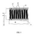
- FIG. 1there is shown a schematic representation of an electronic or opto-electronic device.
- the deviceis fabricated from an interpenetrating network of a nanostructured thin film and a metal, semiconductor, or insulator material forming a large interface area.
- the high surface to volume thin film materialconsisting of an array of nano-protrusions 13 separated by voids is first formed on a conductive substrate or a conductive layer 11 on a substrate 10 (electrode).
- the basic elements of the high surface to volume filmare nano-protrusions as an example. However various other morphologies are possible as long as the nano-scale basic elements each have a continuous charge conduction path to the substrate electrode.
- the void volumeis filled with an appropriate organic/inorganic metal, semiconductor or insulator inter-void material 12 .
- an appropriate electrode 14(or set of electrodes) is defined onto the inter-void material. Thereby each material (nanoprotrusions and matrix) is conformally connected to its own electrode. Contacts to electrodes 15 provide connection to the outside world.
- a wafer (p+Si) 20is a source (+) 21 .
- Al 26is a drain (0) 24 .
- Tri-p-tolylamide 23provides a gate ( ⁇ ) 22 .
- Silicon nano-protrusions (n-type) 25are shown in this embodiment.
- the nanostructured film materialis a comprised of nano-scale basic elements each with the attributes of (1) high surface to volume ratio and (2) electrical connectivity to the substrate electrode.
- the nano-scale basic elementse.g., nanowires, nanocolumns, etc.
- FIG. 1illustrates an example where the film consists of an array of protruding nanocolumns, nanowires, or nanotubes aligned nearly perpendicular to the substrate electrode.
- nano-building-elementscan also be in clusters of sub-elements (e.g., nanoparticles, nanofibers, etc.) that form various nanostructures such as regular nanocolumn or nanowire arrays or fractal coral-like morphologies.
- each elementcan be in the form of a single nanotube or nanowire or a chain of atoms/molecules (i.e., oriented giant molecules).
- the organic/inorganic based appropriate semiconductor, metal or insulator intra-void materialcan be introduced into the void matrix.
- the intra-void materialcan be applied into the high surface to volume film in liquid form, molten, as dissolved in a solvent or by electrochemical means.
- the intra-void materialcan be filled into the voids by exposing the high surface to volume film to the vapor of the intra-void material and subsequent capillary condensation of the vapor inside the voids.
- the intra-void materialoccupies the void network inside the solid porous film, it forms a nanostructured network. Hence each material interpenetrates each other with a nanostructured network creating a large interface area.
- the resulting composite nanostructureconsists of an interpenetrating network of a nanostructured thin film and a metal/semiconductor/ insulator material with a large interface.
- each materialhigh surface to volume film and intra-void material
- FIG. 1A representative illustration of this approach is given in FIG. 1 .
- Organic semiconductor materialsare also called molecular semiconductors since the building blocks are single organic molecules or conjugated polymer molecules.
- photoexcitationcreates electron-hole pairs which are strongly bound (e.g., approximately 0.4 eV in poly(p-phenylenevinylene)).
- Charge collectionrequires the separation of electron and hole into free carriers.
- An exciton(electron-hole pair) can efficiently be split at interfaces between materials with different electron and hole affinities and ionization potentials, where electron is captured by the higher electron affinity side and hole by the lower hole affinity side.
- the lifetime of excitonis short (100-1000 ps), so only excitons created within approximately 10 nm of the interface will ever reach it.
- charge collectiondirectly scales with the interface area, which must be large per unit of light penetrating cross sectional area.
- optimum charge collectionoccurs if continuous conduction pathways are provided to the electrodes for electrons and holes from the interfaces, where they are separated.
- an efficient charge separation and collection devicemay be fabricated from interpenetrating nanostructured thin films and organic semiconductors.
- the high electron affinity difference between inorganic semiconductors (approximately 4 eV) and most organic semiconductors (approximately 3 eV)ensures efficient charge separation at the interface as long as the band gap of the inorganic semiconductor is not smaller than that of the organic semiconductor by the electron affinity difference.
- the nanostructured thin film/organic interfacewill provide an interconnected and extremely large surface for efficient charge photogeneration, separation and collection.
- the interpenetrating network of both inorganic and organicwill provide continuous conduction pathways for electrons and holes to the electrodes. Also, if such a structure is operated with the two electrodes biased, the device will also function as a photodetector. If such a structure is operated under bias and if it is penetrated by adsorbed species, the device will function as a sensor if such penetration changes the device response.
- the nanocrystalshave continuous electrical conduction pathways down to the electrode as proposed in this invention, transport of electrons will not involve tunneling, and they will be transported efficiently by drift or diffusion from where they are photogenerated to where they are collected. Consequently, a higher quantum efficiency can be achieved.
- An attractive feature associated with the large interface formed by interpenetrating network of nanostructured thin films and organic/inorganic semiconductorsis that a very effective electrical contact can be made between the nanostructured film material and the intra-void material. Therefore, light emitting devices can be designed based on efficient carrier injection and subsequent radiative recombination or based on carrier excitation.
- the electron affinity or the hole affinity difference between the two materials at the interfacemay not be in favor of charge injection and rather impede the transport.
- a high band gap layere.g., silicon oxide, silicon nitride
- the conduction band edge (or the valence band edge) of the film materialcan be aligned with the lowest unoccupied molecular orbital (or the highest occupied molecular orbital) of the organic semiconductor material enabling an efficient carrier injection (i.e., by tunneling through the high band-gap material).
- Two conducting nanostructured layerscan be made to sandwich an insulating layer to form a charge capacitor with a high capacitance due to the high surface area of the two layers (electrodes).
- the insulating layershould be thin enough to enable electric fields at highly oblique angles between the two electrode surfaces so that the effective capacitor area is close to that of the interface.
- the insulating layershould also be thick enough to prevent significant charge (current) leakage across electrodes.
- a variety of structurescan be considered to fabricate such a capacitor device with the approach of this invention.
- the following procedurecan be taken: (1) deposition of a highly conductive and porous nanostructured Si thin film with an interconnected void volume (first electrode), (2) coating of the inner surface of the Si film with an oxide by oxidation (i.e., thermal, anodic, or plasma oxidation) or by molecular self-assembly (insulating layer), and (3) filling the void volume with a high conductivity organic semiconductor material conformally covering the oxide surface (second electrode).
- An organometalliccan also be used instead of the organic semiconductor material with a further step of annealing to convert it to a metal.
- the void volume of the film materialcan be filled with an organic insulator, which will planarize the film surface.
- a planar conductive layeris deposited on the organic layer as the second electrode.
- the deposited nanostructured porous filmcan be an insulator deposited on an electrode, or can be made an insulator after deposition by further processing (e.g., Si can be oxidized to obtain SiO 2 ).
- a conductive organic materialcan be applied on the insulating film filling the void volume to generate the second electrode, which will be nanostructured and with a large surface area.
- the nanostructured high surface to volume films of this inventionare ideal for forming ohmic-like contacts to materials systems, in general. This is because their high surface allows many points for carrier transfer.
- the high field that can exist at the nano-scale features of these filmscan give rise to locally very high electric fields and to tunneling.
- This ohmic contact role of these filmscan be combined with their ability to affix molecules to allow our films to serve as ohmic contacts in molecular electronics. This affixing and electrical contacting of molecules can be forced to take place in prescribed locations by patterning techniques and masking.
- a field effect devicecan be fabricated from the composite nanostructure described in this invention wherein the electric current through said nanoprotrusions of the porous film is regulated by varying the electric potential of the intra-void material surrounding the nanoprotrusions.
- the nanoprotrusionsmust be connected to a second electrode in addition to the electrode at their base for the flow of electric current and therefore the resulting device consists of three electrical contacts. Therefore, the nanoprotrusions serve as the channel and the electrodes they are connected to as source and drain, whereas at least a portion of the intra-void material serves as the gate of this field effect transistor.
- any currents between the gate and channel, source or drainwill be leakage currents and therefore must be minimized.
- Thiscan be achieved by isolating the conducting intra-void material from other regions with a high band-gap material layer at the interfaces.
- the nano-protrusionsare Si, their surface may be oxidized to insulate them from the filling material (gate) with an interfacial silicon oxide layer.
- self assembling moleculescan be attached to the interface to serve as the required insulator layer.
- Another approachwould be to use a highly doped high band-gap material for the filling material (gate).
- FIG. 2depicts an example device with Si nanoprotrusions and tri-p-tolylamine, a highly doped high band-gap material, as the filling material (gate).
- the gatewhen the gate is negatively biased it will invert the Si protrusions to be hole carriers and significantly enhance the hole current from source (p Si) to drain (Al) (turning on the transistor).
- the leakage hole currents from Si or Al to tri-p-tolylaminewill be impeded by the significant differences in ionization potentials at the interfaces (>1 eV).
- the leakage electron currents from tri-p-tolylamine to Si or Alwill be insignificant, since tri-p-tolylamine is a hole transport material and is depleted of electrons.
- a structure based on this concept of the electrically contacted high surface to volume film and intra-void material with its electrical contact(s) such as seen in FIG. 1can also be used as a chemical sensor. Sensing will occur when the species to be detected interact with the intra-void material thereby modifying its electrical or dielectric properties resulting in a change in the ac or dc behavior observed though the electrical contacts.
Landscapes
- Chemical & Material Sciences (AREA)
- Physics & Mathematics (AREA)
- Engineering & Computer Science (AREA)
- Nanotechnology (AREA)
- Inorganic Chemistry (AREA)
- Electromagnetism (AREA)
- Crystallography & Structural Chemistry (AREA)
- Optics & Photonics (AREA)
- Mathematical Physics (AREA)
- Theoretical Computer Science (AREA)
- Light Receiving Elements (AREA)
- Thin Film Transistor (AREA)
Abstract
Description
This application claims priority from U.S. Provisional Application No. 60/296,857, filed Jun. 8, 2001 and U.S. patent application, Ser. No. 10/144,456, filed on May 13, 2002, which is a Continuation-In-Part of U.S. patent application, Ser. No. 10/104,749, filed on Mar. 22, 2002, which is a Continuation of U.S. patent application, Ser. No. 09/580,105, filed on May 30, 2000, now U.S. Pat. No. 6,399,177.
1. Field of the Invention
The present invention generally relates to a novel production method for the production of electronic and opto-electronic devices from an interpenetrating network configuration of nano structured high surface to volume ratio porous thin films with organic/inorganic metal, semiconductor or insulator material positioned within the interconnected void volume of the nano structure.
2. Description of the Prior Art
Today nanoparticles are proposed for, and used for, providing a high surface area to volume ratio material. Besides the large surface area they provide, nanoparticles can be embedded in organic/inorganic semiconductor/insulator materials (nano composite systems) to obtain a high interface area that can be exploited in, for example, the following optoelectronic and electronic applications: (a) charge separation functions for such applications as photovoltaics and detectors; (b) charge injection functions for such applications as light emitting devices; (c) charge storage functions for capacitors; and (d) ohmic contact-like functions for such applications as contacting molecular electronic structures.
There are difficulties with nanoparticles, however. These include their handling and, for electronic and opto-electronic uses, they also include the question of how to achieve electrical contact. The present invention solves these two problems by using deposited nanostructured high surface to volume ratio materials. These materials allow a manageable high interface area which is easily contacted electrically.
In the present approach for making optoelectronic devices from nanoparticle composite systems isolated nanoparticles are diffused into a matrix of organic material. Ideally, each nanoparticle or nanoparticle surface must be electrically connected to the outside (by a set of electrodes) for electrical and opto-electronic function. This is best achieved if the nanoparticles are arranged so that they are interconnected to the electrodes providing continuous electrical pathways to these particles. However, in the present art with the use of isolated nanoparticles, these particles will often fail to make good electrical contacts even if the volume fraction of nanoparticles is made close to unity.
In this invention a different approach is proposed to avoid this problem. This approach involves formation of a thin film of a nanostructured high surface area to volume ratio material on an electrode substrate or a patterned set of electrodes on a substrate. The basic elements (building blocks) of this nanostructure are embedded in an interconnected void matrix with the attributes of high surface to volume ratio but with electrical connectivity to the substrate electrode. Once the interconnected void network of this film material is filled with a secondary material a composite is formed with high interface area. Furthermore, each component of the composite structure is conformally connected. Hence, any region of the composite system including the interface has continuous electrical connection to the outside.
A method of fabricating an electronic/optoelectronic device from an interpenetrating network of a nanostructured high surface area to volume ratio material and an organic/inorganic matrix material comprising the steps of: a) obtaining a high surface area to volume ratio film material onto an electrode substrate (or a patterned electrode substrate), such that any region of this film material is in electrical connectivity with the electrode substrate by virtue of the morphology. For example, the film material may comprise an array of nano and/or micro-protrusions electrically connected to the electrode substrate and separated by a void matrix; b) filling the void matrix of the high surface to volume film with an organic/inorganic solid or liquid material; and c) defining an electrode or set of electrodes onto the organic or inorganic intra-void material embedded in said void matrix.
The basic elements of the high surface area to volume film material can be selected from the group consisting of: nanotubes, nanorods, nanowires, nanocolumns or aggregates thereof, oriented molecules, chains of atoms, chains of molecules, fullerenes, nanoparticles, aggregates of nanoparticles, and any combinations thereof.
The organic/inorganic intra-void material is at least one selected from the group consisting of: organic semiconductor material, organic insulator material, inorganic semiconductor material, inorganic insulator material, conjugated polymers, metals, organometallics, self assembling molecular layers and any combinations thereof.
The high surface area to volume porous film is preferably deposited onto the conductive (electrode) substrate or on a patterned substrate by, for example, chemical vapor deposition, plasma-enhanced chemical vapor deposition, physical vapor deposition, or electrodeposition. Or it may be obtained by electrochemical etching.
The organic or inorganic intra-void material may be applied into the void matrix in liquid form, molten form, as dissolved in a solvent, or by electrochemical means. Additionally, the intra-void material may be embedded into the void matrix by exposing the film material to the vapor of the intra-void material, thus causing the vapor to condense inside the void matrix.
The interpenetrating network of nanostructured high surface area to volume ratio material and intra-void material may be used for fabricating a charge separation and collection device such as a chemical sensor, photodetector or a photovoltaic device.
The network may also be used for fabricating a charge injection device such as an electroluminescent device.
The interpenetrating network of nanostructured high surface area to volume ratio material and organic/inorganic intra-void material may also be used for fabricating a charge storage device (capacitor).
The nanostructured high surface area to volume ratio material may also be used as an ohmic-like contact to the intra-void material.
The interpenetrating network of nanostructured high surface area to volume ratio material and intra-void material may further be used to fabricate an electronic device in which the electronic current through the nano-scale basic elements of the film (charge transport paths) are regulated by the electric potential applied to the filling material surrounding the nano-scale basic elements or vice versa. This electronic device functions as a field effect-type transistor.
Other features and advantages of the present invention will be apparent from the following detailed description and from the claims.
The present invention is directed to a method for fabricating an interpenetrating network of a nanostructured high surface area to volume ratio material and an organic or inorganic intra-void material comprising: a) obtaining a high surface area to volume ratio film material onto an electrode substrate (or a patterned electrode substrate), such that any region of this film material is in electrical connectivity with the electrode substrate by virtue of the morphology. For example, the film material may comprise an array of nano and/or micro-protrusions electrically connected to the electrode substrate and separated by a void matrix; b) filling the void matrix of the high surface to volume film with an organic/inorganic solid or liquid material; and c) defining an electrode or set of electrodes onto the organic or inorganic intra-void material embedded in said void matrix.
The basic elements of the high surface area to volume film material can be selected from the group consisting of: nanotubes, nanorods, nanowires, nanocolumns or aggregates thereof, oriented molecules, chains of atoms, chains of molecules, fullerenes, nanoparticles, aggregates of nanoparticles, and any combinations thereof. The basic elements of the high surface area to volume film comprises a material selected from the group consisting of: silicon, silicon dioxide, germanium, germanium oxide, indium, gallium, cadmium, selenium, tellurium, and alloys and compounds thereof, carbon, hydrogen, semiconductors, insulators, metals, ceramics, polymers, other inorganic material, organic material, or any combinations thereof.
The organic/inorganic filling material may comprise a semiconductor, an insulator, a metal, an organometallic, a self assembling molecular layer, a conjugated polymer, and any combinations thereof.
The high surface area to volume porous film is preferably deposited onto the conductive (electrode) substrate or on a patterned substrate by, for example, chemical vapor deposition, plasma-enhanced chemical vapor deposition, physical vapor deposition, or electrodeposition. Or it may be obtained by electrochemical etching.
The organic or inorganic intra-void material may be applied into the void matrix in liquid form, molten form as dissolved in a solvent, or by electrochemical means. Additionally, the intra-void material may be embedded into the void matrix by exposing the film material to the vapor of the intra-void material, thus causing the vapor to condense inside the void matrix.
Referring now toFIG. 1 , there is shown a schematic representation of an electronic or opto-electronic device. The device is fabricated from an interpenetrating network of a nanostructured thin film and a metal, semiconductor, or insulator material forming a large interface area. The high surface to volume thin film material consisting of an array of nano-protrusions 13 separated by voids is first formed on a conductive substrate or aconductive layer 11 on a substrate10 (electrode). Here, the basic elements of the high surface to volume film are nano-protrusions as an example. However various other morphologies are possible as long as the nano-scale basic elements each have a continuous charge conduction path to the substrate electrode. Then the void volume is filled with an appropriate organic/inorganic metal, semiconductor or insulatorinter-void material 12. Finally, an appropriate electrode14 (or set of electrodes) is defined onto the inter-void material. Thereby each material (nanoprotrusions and matrix) is conformally connected to its own electrode. Contacts toelectrodes 15 provide connection to the outside world.
Referring toFIG. 2 , a wafer (p+Si)20 is a source (+)21.Al 26 is a drain (0)24. Tri-p-tolylamide 23 provides a gate (−)22. Silicon nano-protrusions (n-type)25 are shown in this embodiment.
In the devices of the present invention, the nanostructured film material is a comprised of nano-scale basic elements each with the attributes of (1) high surface to volume ratio and (2) electrical connectivity to the substrate electrode. The nano-scale basic elements (e.g., nanowires, nanocolumns, etc.) are separated by voids, or equivalently they are embedded in an interconnected void matrix.FIG. 1 illustrates an example where the film consists of an array of protruding nanocolumns, nanowires, or nanotubes aligned nearly perpendicular to the substrate electrode. These nano-building-elements can also be in clusters of sub-elements (e.g., nanoparticles, nanofibers, etc.) that form various nanostructures such as regular nanocolumn or nanowire arrays or fractal coral-like morphologies. Or, each element can be in the form of a single nanotube or nanowire or a chain of atoms/molecules (i.e., oriented giant molecules).
In the approach of this invention, after the formation of the film of nano-scale elements, the organic/inorganic based appropriate semiconductor, metal or insulator intra-void material can be introduced into the void matrix. Here, the intra-void material can be applied into the high surface to volume film in liquid form, molten, as dissolved in a solvent or by electrochemical means. Furthermore, the intra-void material can be filled into the voids by exposing the high surface to volume film to the vapor of the intra-void material and subsequent capillary condensation of the vapor inside the voids. Once the intra-void material occupies the void network inside the solid porous film, it forms a nanostructured network. Hence each material interpenetrates each other with a nanostructured network creating a large interface area.
To complete the fabrication of a chemical sensor, electronic or opto-electronic device, a step finally defining an appropriate electrode to the intra-void material would be undertaken. Thus, the resulting composite nanostructure consists of an interpenetrating network of a nanostructured thin film and a metal/semiconductor/ insulator material with a large interface. In this approach of this invention, each material (high surface to volume film and intra-void material) is conformally connected to its own electrode. A representative illustration of this approach is given in FIG.1.
The invention is further illustrated by the following examples which are intended for illustration and not for limitation of the scope thereof.
(Charge Separation and Photovoltaics)
Organic semiconductor materials are also called molecular semiconductors since the building blocks are single organic molecules or conjugated polymer molecules. In molecular semiconductors, photoexcitation creates electron-hole pairs which are strongly bound (e.g., approximately 0.4 eV in poly(p-phenylenevinylene)). Charge collection requires the separation of electron and hole into free carriers.
An exciton (electron-hole pair) can efficiently be split at interfaces between materials with different electron and hole affinities and ionization potentials, where electron is captured by the higher electron affinity side and hole by the lower hole affinity side. Unfortunately, the lifetime of exciton is short (100-1000 ps), so only excitons created within approximately 10 nm of the interface will ever reach it. Accordingly, charge collection directly scales with the interface area, which must be large per unit of light penetrating cross sectional area. Furthermore, optimum charge collection occurs if continuous conduction pathways are provided to the electrodes for electrons and holes from the interfaces, where they are separated.
Hence, an efficient charge separation and collection device may be fabricated from interpenetrating nanostructured thin films and organic semiconductors. For example, the high electron affinity difference between inorganic semiconductors (approximately 4 eV) and most organic semiconductors (approximately 3 eV) ensures efficient charge separation at the interface as long as the band gap of the inorganic semiconductor is not smaller than that of the organic semiconductor by the electron affinity difference. Furthermore, the nanostructured thin film/organic interface will provide an interconnected and extremely large surface for efficient charge photogeneration, separation and collection.
The interpenetrating network of both inorganic and organic will provide continuous conduction pathways for electrons and holes to the electrodes. Also, if such a structure is operated with the two electrodes biased, the device will also function as a photodetector. If such a structure is operated under bias and if it is penetrated by adsorbed species, the device will function as a sensor if such penetration changes the device response.
Our approach of a thin film of protrusions (of nanoparticles or clusters of nanoparticles) with high surface to volume ratio has many advantages over the use of individual nanoparticles, as is practiced in the art. For example, Greenham et al. have reported a photovoltaic device based on CdSe nanocrystals embedded in a matrix of a semiconductor polymer, poly(2-methoxy,5-(2′-ethyl-hexyloxy)-p-phenylenevinylene). Both materials are semiconductors with band-gaps of about 2 eV, but the electron affinity of the nanocrystals is much greater than that of the polymer. As a result, electron-hole pairs generated by photons (either in the nanocrystals or the polymer) rapidly separate with the hole residing on the polymer and the electron on the nanocrystals. Then, free holes move along the polymer phase (diffusion or drift), while free electrons hop (tunnel) from nanocrystal to nanocrystal until they are collected at electrodes.
In this device, the mechanism of electron transport being tunneling between nanocrystals (i.e., effectively a slow process) limits the collection efficiency of electrons. Slow transport of electrons also increases their probability of recombining with holes before being collected. As a result of this poor carrier collection, the highest quantum efficiency achievable with this discrete nanoparticle approach was only around 12% (i.e., 12% at 514 nm).
On the other hand, if the nanocrystals have continuous electrical conduction pathways down to the electrode as proposed in this invention, transport of electrons will not involve tunneling, and they will be transported efficiently by drift or diffusion from where they are photogenerated to where they are collected. Consequently, a higher quantum efficiency can be achieved.
(Charge Injection and Light Emitting Devices)
An attractive feature associated with the large interface formed by interpenetrating network of nanostructured thin films and organic/inorganic semiconductors is that a very effective electrical contact can be made between the nanostructured film material and the intra-void material. Therefore, light emitting devices can be designed based on efficient carrier injection and subsequent radiative recombination or based on carrier excitation.
On the other hand, the electron affinity or the hole affinity difference between the two materials at the interface may not be in favor of charge injection and rather impede the transport. In this situation, a high band gap layer (e.g., silicon oxide, silicon nitride), which is thin enough (i.e., 20-60 Å) for carriers to tunnel can be placed at the interface. Since the voltage drop and band bending will mostly occur across this high band-gap layer, the conduction band edge (or the valence band edge) of the film material can be aligned with the lowest unoccupied molecular orbital (or the highest occupied molecular orbital) of the organic semiconductor material enabling an efficient carrier injection (i.e., by tunneling through the high band-gap material).
(Charge Capacitors)
Two conducting nanostructured layers can be made to sandwich an insulating layer to form a charge capacitor with a high capacitance due to the high surface area of the two layers (electrodes). In this application, the insulating layer should be thin enough to enable electric fields at highly oblique angles between the two electrode surfaces so that the effective capacitor area is close to that of the interface. However, the insulating layer should also be thick enough to prevent significant charge (current) leakage across electrodes.
A variety of structures can be considered to fabricate such a capacitor device with the approach of this invention. As an example, the following procedure can be taken: (1) deposition of a highly conductive and porous nanostructured Si thin film with an interconnected void volume (first electrode), (2) coating of the inner surface of the Si film with an oxide by oxidation (i.e., thermal, anodic, or plasma oxidation) or by molecular self-assembly (insulating layer), and (3) filling the void volume with a high conductivity organic semiconductor material conformally covering the oxide surface (second electrode). An organometallic can also be used instead of the organic semiconductor material with a further step of annealing to convert it to a metal.
Additionally, only one of the electrodes could be made to have nanostructured surface (high surface area). This can simply be obtained as follows: after the step (1) as above, the void volume of the film material can be filled with an organic insulator, which will planarize the film surface. Then a planar conductive layer is deposited on the organic layer as the second electrode. Furthermore, the deposited nanostructured porous film can be an insulator deposited on an electrode, or can be made an insulator after deposition by further processing (e.g., Si can be oxidized to obtain SiO2). Then a conductive organic material can be applied on the insulating film filling the void volume to generate the second electrode, which will be nanostructured and with a large surface area.
(Ohmic-like Contacts)
The nanostructured high surface to volume films of this invention are ideal for forming ohmic-like contacts to materials systems, in general. This is because their high surface allows many points for carrier transfer. In addition the high field that can exist at the nano-scale features of these films can give rise to locally very high electric fields and to tunneling. This ohmic contact role of these films can be combined with their ability to affix molecules to allow our films to serve as ohmic contacts in molecular electronics. This affixing and electrical contacting of molecules can be forced to take place in prescribed locations by patterning techniques and masking.
(Field Effect Devices)
A field effect device can be fabricated from the composite nanostructure described in this invention wherein the electric current through said nanoprotrusions of the porous film is regulated by varying the electric potential of the intra-void material surrounding the nanoprotrusions. In this case, the nanoprotrusions must be connected to a second electrode in addition to the electrode at their base for the flow of electric current and therefore the resulting device consists of three electrical contacts. Therefore, the nanoprotrusions serve as the channel and the electrodes they are connected to as source and drain, whereas at least a portion of the intra-void material serves as the gate of this field effect transistor. While at least a portion of the intra-void material must be a good electrical conductor (gate), any currents between the gate and channel, source or drain will be leakage currents and therefore must be minimized. This can be achieved by isolating the conducting intra-void material from other regions with a high band-gap material layer at the interfaces. For example, if the nano-protrusions are Si, their surface may be oxidized to insulate them from the filling material (gate) with an interfacial silicon oxide layer. Alternatively, self assembling molecules can be attached to the interface to serve as the required insulator layer. Another approach would be to use a highly doped high band-gap material for the filling material (gate). This will ensure a uniform electric potential throughout the gate material, while the leakage currents will be minimized due to either band offsets or depletion of minority carriers in the gate material.FIG. 2 depicts an example device with Si nanoprotrusions and tri-p-tolylamine, a highly doped high band-gap material, as the filling material (gate). Here when the gate is negatively biased it will invert the Si protrusions to be hole carriers and significantly enhance the hole current from source (p Si) to drain (Al) (turning on the transistor). The leakage hole currents from Si or Al to tri-p-tolylamine will be impeded by the significant differences in ionization potentials at the interfaces (>1 eV). On the other hand, the leakage electron currents from tri-p-tolylamine to Si or Al will be insignificant, since tri-p-tolylamine is a hole transport material and is depleted of electrons.
Although the present invention describes in detail certain embodiments, it is understood that variations and modifications exist known to those skilled in the art that are within the invention. Accordingly, the present invention is intended to encompass all such alternatives, modifications and variations that are within the scope of the invention as set forth in the following claims.
(Chemical Sensors)
A structure based on this concept of the electrically contacted high surface to volume film and intra-void material with its electrical contact(s) such as seen inFIG. 1 can also be used as a chemical sensor. Sensing will occur when the species to be detected interact with the intra-void material thereby modifying its electrical or dielectric properties resulting in a change in the ac or dc behavior observed though the electrical contacts.
Claims (21)
1. An electronic or opto-electronic device comprising:
a first conductive layer;
a nanostructured high surface area to volume ratio film material disposed on said first conductive layer, such that nano-scale elements of said film material are disposed in an interconnected void matrix and wherein each said nano-scale element has electrical connectivity with the said first conductive layer;
an organic or inorganic intra-void material filled into said continuous void volume of said nanostructured high surface area to volume ratio film defining an interface between the intra-void material and each of the nano-scale elements; and
a second conductive layer electrode in contact with said intra-void material;
wherein charge separation, charge injection or charge storage occurs at said interface.
2. The electronic or opto-electronic device ofclaim 1 , wherein said first and second conductive layers are at least one material selected from the group consisting of: semiconductors, glasses, plastics, polymers, metals, ceramics, partially conducting insulators, organic materials, inorganic materials, or any combinations thereof.
3. The electronic or opto-electronic device ofclaim 1 , wherein said nano-scale elements are at least one selected from the group consisting of: nanotubes, nanorods, nanowires, nanocolumns or aggregates thereof, oriented molecules, chains of atoms, chains of molecules, nanoparticles, aggregates of nanoparticles, and any combinations thereof.
4. The electronic or opto-electronic device ofclaim 1 , wherein said organic and inorganic material is at least one selected from the group consisting of: organic semiconductor material, organic insulator material, inorganic semiconductor material, inorganic insulator material, conjugated polymers, metals, organometallics, self assembling molecular layers and any combinations thereof.
5. The electronic or opto-electronic device ofclaim 1 , wherein said electronic or opto-electronic device is selected from the group consisting of charge separation and photovoltaic devices, charge injection and electroluminescent devices; charge capacitor devices, ohmic-like contact devices, and field effect devices.
6. The electronic or opto-electronic device ofclaim 1 , wherein said nano-scale elements are formed of a material selected from the group consisting of: silicon, silicon dioxide, germanium, germanium oxide, indium, gallium, cadmium, selenium, tellurium, and alloys and compounds thereof, carbon, hydrogen, semiconductors, insulators, metals, ceramics, polymers, other inorganic material, organic material, or any combinations thereof.
7. The electronic or opto-electronic device ofclaim 1 , wherein said nano-scale elements have a diameter of between about 1 to 50 nm.
8. The electronic or opto-electronic device according toclaim 1 , wherein said nano-scale material is deposited.
9. The electronic or opto-electronic device according toclaim 8 , wherein said nano-scale material is formed by at least one process selected from the group consisting of: chemical vapor deposition, physical vapor deposition, electrochemical etching and electrode position.
10. The electronic or opto-electronic device according toclaim 1 , wherein said deposited nano-scale material is formed by means comprising use of a high-density plasma.
11. The electronic or opto-electronic device according toclaim 1 , wherein said electronic or opto-electronic device is a light emitting device and wherein a high band gap layer having a thickness of between about 20-60 Å is disposed between the interface between said nano-scale material and said an organic or inorganic intra-void material.
12. The electronic or opto-electronic device according toclaim 1 , wherein said nano-scale composition has a thickness greater than 10 nm.
13. The electronic or opto-electronic device according toclaim 1 , wherein said nano-scale elements are rod-like perturbations that are agglomerations of adjustably sized columnar-like clusters adhered to said first conductive layer.
14. The electronic or opto-electronic device according toclaim 1 , wherein the interface between said nano-scale material and said organic material provides an interconnected surface for charge photogeneration, separation and collection.
15. The electronic or opto-electronic device according toclaim 1 , wherein said organic or inorganic material provides a continuous conduction pathway for electrons and holes to said first and second conductive layers.
16. The electronic or opto-electronic device according toclaim 1 , wherein said first and second conductive layers are biased, whereby said device functions as a photodetector.
17. A charge capacitor comprising:
a first conductive layer;
a nano-scale composition comprising a plurality of polycrystalline or amorphous rod-like perturbations penetrating a continuous void, wherein said plurality of rod-like perturbations are uniformly orientated and adhered to said first conductive layer;
an organic or inorganic intra-void material disposed within continuous void of said nano-scale composition; and
a second conductive layer conformally covering said insulating material disposed within said continuous void of said nano-scale composition.
18. The charge capacitor according toclaim 17 , wherein said first conductive layer is silicon and said second conductive layer is either an organic semiconductor material or an organometallic material.
19. An electronic or opto-electronic device comprising:
a first conductive layer;
a nano-scale composition comprising a plurality of polycrystalline or amorphous rod-like perturbations penetrating a continuous void, wherein said plurality of rod-like perturbations are uniformly orientated and adhered to said first conductive layer;
an insulating material disposed within continuous void of said nano-scale composition; and
a second conductive layer conformally covering said insulating material disposed within said continuous void of said nano-scale composition.
20. The electronic of opto-electronic device ofclaim 19 , wherein the device is a charge capacitor.
21. The electronic or opto-electronic device according toclaim 1 , wherein said nano-scale composition has a thickness greater than 1 nm.
Priority Applications (4)
| Application Number | Priority Date | Filing Date | Title |
|---|---|---|---|
| US10/165,858US6919119B2 (en) | 2000-05-30 | 2002-06-08 | Electronic and opto-electronic devices fabricated from nanostructured high surface to volume ratio thin films |
| US11/080,066US7341774B2 (en) | 2000-05-30 | 2005-03-14 | Electronic and opto-electronic devices fabricated from nanostructured high surface to volume ratio thin films |
| US11/972,491US8294025B2 (en) | 2002-06-08 | 2008-01-10 | Lateral collection photovoltaics |
| US13/657,035US9634163B2 (en) | 2002-06-08 | 2012-10-22 | Lateral collection photovoltaics |
Applications Claiming Priority (5)
| Application Number | Priority Date | Filing Date | Title |
|---|---|---|---|
| US09/580,105US6399177B1 (en) | 1999-06-03 | 2000-05-30 | Deposited thin film void-column network materials |
| US29685701P | 2001-06-08 | 2001-06-08 | |
| US10/104,749US20020132101A1 (en) | 1999-06-03 | 2002-03-22 | Deposited thin film void-column network materials |
| US10/144,456US7122790B2 (en) | 2000-05-30 | 2002-05-13 | Matrix-free desorption ionization mass spectrometry using tailored morphology layer devices |
| US10/165,858US6919119B2 (en) | 2000-05-30 | 2002-06-08 | Electronic and opto-electronic devices fabricated from nanostructured high surface to volume ratio thin films |
Related Parent Applications (1)
| Application Number | Title | Priority Date | Filing Date |
|---|---|---|---|
| US10/144,456Continuation-In-PartUS7122790B2 (en) | 2000-05-30 | 2002-05-13 | Matrix-free desorption ionization mass spectrometry using tailored morphology layer devices |
Related Child Applications (2)
| Application Number | Title | Priority Date | Filing Date |
|---|---|---|---|
| US11/080,066Continuation-In-PartUS7341774B2 (en) | 2000-05-30 | 2005-03-14 | Electronic and opto-electronic devices fabricated from nanostructured high surface to volume ratio thin films |
| US11/080,066ContinuationUS7341774B2 (en) | 2000-05-30 | 2005-03-14 | Electronic and opto-electronic devices fabricated from nanostructured high surface to volume ratio thin films |
Publications (2)
| Publication Number | Publication Date |
|---|---|
| US20020192441A1 US20020192441A1 (en) | 2002-12-19 |
| US6919119B2true US6919119B2 (en) | 2005-07-19 |
Family
ID=34753852
Family Applications (2)
| Application Number | Title | Priority Date | Filing Date |
|---|---|---|---|
| US10/165,858Expired - Fee RelatedUS6919119B2 (en) | 2000-05-30 | 2002-06-08 | Electronic and opto-electronic devices fabricated from nanostructured high surface to volume ratio thin films |
| US11/080,066Expired - LifetimeUS7341774B2 (en) | 2000-05-30 | 2005-03-14 | Electronic and opto-electronic devices fabricated from nanostructured high surface to volume ratio thin films |
Family Applications After (1)
| Application Number | Title | Priority Date | Filing Date |
|---|---|---|---|
| US11/080,066Expired - LifetimeUS7341774B2 (en) | 2000-05-30 | 2005-03-14 | Electronic and opto-electronic devices fabricated from nanostructured high surface to volume ratio thin films |
Country Status (1)
| Country | Link |
|---|---|
| US (2) | US6919119B2 (en) |
Cited By (80)
| Publication number | Priority date | Publication date | Assignee | Title |
|---|---|---|---|---|
| US20050179052A1 (en)* | 2004-02-12 | 2005-08-18 | Yi Gyu C. | Heterojunction structure of nitride semiconductor and nano-device or an array thereof comprising same |
| US20050269576A1 (en)* | 2004-06-05 | 2005-12-08 | Samsung Electronics Co., Ltd. | Light-emitting device using nano size needle |
| US20060057354A1 (en)* | 2000-05-30 | 2006-03-16 | Penn State Research Foundation | Electronic and opto-electronic devices fabricated from nanostructured high surface to volume ratio thin films |
| US20060110618A1 (en)* | 2004-11-24 | 2006-05-25 | General Electric Company | Electrodes for photovoltaic cells and methods for manufacture thereof |
| US20060174934A1 (en)* | 2002-11-05 | 2006-08-10 | Nanosolar, Inc. | Optoelectronic device and frabrication method |
| US20060199313A1 (en)* | 2003-01-30 | 2006-09-07 | University Of Cape Town | Thin film semiconductor device and method of manufacturing a thin film semiconductor device |
| US20070102809A1 (en)* | 2003-06-25 | 2007-05-10 | Dubin Valery M | Methods of fabricating a composite carbon nanotube thermal interface device |
| WO2007062527A1 (en)* | 2005-11-30 | 2007-06-07 | The Governors Of The University Of Alberta | Organic columnar thin films |
| US20070139976A1 (en)* | 2005-06-30 | 2007-06-21 | Derochemont L P | Power management module and method of manufacture |
| US20070170535A1 (en)* | 2006-01-24 | 2007-07-26 | De Rochemont L Pierre | Photovoltaic devices with silicon dioxide encapsulation layer and method to make same |
| US20070171596A1 (en)* | 2006-01-20 | 2007-07-26 | Chacko Antony P | Electrode compositions containing carbon nanotubes for solid electrolyte capacitors |
| US7253017B1 (en)* | 2002-06-22 | 2007-08-07 | Nanosolar, Inc. | Molding technique for fabrication of optoelectronic devices |
| US20070194694A1 (en)* | 2006-02-17 | 2007-08-23 | Solexant Corp | Nanostructured electroluminescent device and display |
| US20080006883A1 (en)* | 2006-06-26 | 2008-01-10 | Matsushita Electric Industrial Co., Ltd. | Nanostructured integrated circuits with capacitors |
| US20080176030A1 (en)* | 2002-06-08 | 2008-07-24 | Fonash Stephen J | Lateral collection photovoltaics |
| US20090000663A1 (en)* | 2007-04-04 | 2009-01-01 | Sungkyunkwan University Foundation For Corporate Collaboration | Dye-sensitized solar cell and method of manufacturing the same |
| US20090050204A1 (en)* | 2007-08-03 | 2009-02-26 | Illuminex Corporation. | Photovoltaic device using nanostructured material |
| US20090085512A1 (en)* | 2007-09-27 | 2009-04-02 | Motorola, Inc. | Apparatus for charging a battery of a portable electronic device |
| US20090159131A1 (en)* | 2007-12-19 | 2009-06-25 | Honeywell International Inc. | Quantum dot solar cell with rigid bridge molecule |
| US20090159999A1 (en)* | 2007-12-19 | 2009-06-25 | Honeywell International Inc. | Quantum dot solar cell with electron rich anchor group |
| US20090159120A1 (en)* | 2007-12-19 | 2009-06-25 | Honeywell International Inc. | Quantum dot solar cell with conjugated bridge molecule |
| US20090159124A1 (en)* | 2007-12-19 | 2009-06-25 | Honeywell International Inc. | Solar cell hyperpolarizable absorber |
| US20090211634A1 (en)* | 2008-02-26 | 2009-08-27 | Honeywell International Inc. | Quantum dot solar cell |
| US20090217963A1 (en)* | 2008-02-29 | 2009-09-03 | Motorola, Inc. | Photovoltaic apparatus for charging a portable electronic device and method for making |
| US20090260682A1 (en)* | 2008-04-22 | 2009-10-22 | Honeywell International Inc. | Quantum dot solar cell |
| US20090260683A1 (en)* | 2008-04-22 | 2009-10-22 | Honeywell International Inc. | Quantum dot solar cell |
| US20090266411A1 (en)* | 2005-06-17 | 2009-10-29 | Illuminex Corporation | Photovoltaic wire |
| US20090283142A1 (en)* | 2008-05-13 | 2009-11-19 | Honeywell International Inc. | Quantum dot solar cell |
| US20100006148A1 (en)* | 2008-07-08 | 2010-01-14 | Honeywell International Inc. | Solar cell with porous insulating layer |
| US20100012191A1 (en)* | 2008-07-15 | 2010-01-21 | Honeywell International Inc. | Quantum dot solar cell |
| US20100012168A1 (en)* | 2008-07-18 | 2010-01-21 | Honeywell International | Quantum dot solar cell |
| US20100041177A1 (en)* | 2006-07-11 | 2010-02-18 | The Trustees Of The Princeton University | Controlled growth of larger heterojunction interface area for organic photosensitive devices |
| US20100193026A1 (en)* | 2009-02-04 | 2010-08-05 | Honeywell International Inc. | Quantum dot solar cell |
| US20100193768A1 (en)* | 2005-06-20 | 2010-08-05 | Illuminex Corporation | Semiconducting nanowire arrays for photovoltaic applications |
| US20100193025A1 (en)* | 2009-02-04 | 2010-08-05 | Honeywell International Inc. | Quantum dot solar cell |
| US7794828B1 (en)* | 2005-02-01 | 2010-09-14 | Hrl Laboratories, Llc | Directional and areal thermal control coating, using aligned metal oxide mesostructures |
| US20100258163A1 (en)* | 2009-04-14 | 2010-10-14 | Honeywell International Inc. | Thin-film photovoltaics |
| US20100275985A1 (en)* | 2009-04-30 | 2010-11-04 | Honeywell International Inc. | Electron collector and its application in photovoltaics |
| US20100313957A1 (en)* | 2009-06-12 | 2010-12-16 | Honeywell International Inc. | Quantum dot solar cells |
| US20100326499A1 (en)* | 2009-06-30 | 2010-12-30 | Honeywell International Inc. | Solar cell with enhanced efficiency |
| US20110021007A1 (en)* | 2006-01-24 | 2011-01-27 | De Rochemont L Pierre | Liquid chemical depostion apparatus and process and products therefrom |
| US20110023955A1 (en)* | 2007-06-26 | 2011-02-03 | Fonash Stephen J | Lateral collection photovoltaics |
| US20110108102A1 (en)* | 2009-11-06 | 2011-05-12 | Honeywell International Inc. | Solar cell with enhanced efficiency |
| US7956525B2 (en) | 2003-05-16 | 2011-06-07 | Nanomix, Inc. | Flexible nanostructure electronic devices |
| US20110139233A1 (en)* | 2009-12-11 | 2011-06-16 | Honeywell International Inc. | Quantum dot solar cell |
| US20110139248A1 (en)* | 2009-12-11 | 2011-06-16 | Honeywell International Inc. | Quantum dot solar cells and methods for manufacturing solar cells |
| US20110146777A1 (en)* | 2009-12-21 | 2011-06-23 | Honeywell International Inc. | Counter electrode for solar cell |
| US20110155233A1 (en)* | 2009-12-29 | 2011-06-30 | Honeywell International Inc. | Hybrid solar cells |
| US20110174364A1 (en)* | 2007-06-26 | 2011-07-21 | Honeywell International Inc. | nanostructured solar cell |
| US8178457B2 (en) | 2004-10-01 | 2012-05-15 | De Rochemont L Pierre | Ceramic antenna module and methods of manufacture thereof |
| US8264137B2 (en) | 2006-01-03 | 2012-09-11 | Samsung Electronics Co., Ltd. | Curing binder material for carbon nanotube electron emission cathodes |
| US8455757B2 (en) | 2008-08-20 | 2013-06-04 | Honeywell International Inc. | Solar cell with electron inhibiting layer |
| US8552708B2 (en) | 2010-06-02 | 2013-10-08 | L. Pierre de Rochemont | Monolithic DC/DC power management module with surface FET |
| US8715839B2 (en) | 2005-06-30 | 2014-05-06 | L. Pierre de Rochemont | Electrical components and method of manufacture |
| US20140126165A1 (en)* | 2012-11-06 | 2014-05-08 | Infineon Technologies Austria Ag | Packaged Nano-Structured Component and Method of Making a Packaged Nano-Structured Component |
| US8749054B2 (en) | 2010-06-24 | 2014-06-10 | L. Pierre de Rochemont | Semiconductor carrier with vertical power FET module |
| US8779489B2 (en) | 2010-08-23 | 2014-07-15 | L. Pierre de Rochemont | Power FET with a resonant transistor gate |
| US8779413B1 (en) | 2012-10-09 | 2014-07-15 | Sunpower Technologies Llc | Optoelectronic devices with all-inorganic colloidal nanostructured films |
| US8922347B1 (en) | 2009-06-17 | 2014-12-30 | L. Pierre de Rochemont | R.F. energy collection circuit for wireless devices |
| US8952858B2 (en) | 2009-06-17 | 2015-02-10 | L. Pierre de Rochemont | Frequency-selective dipole antennas |
| US9023493B2 (en) | 2010-07-13 | 2015-05-05 | L. Pierre de Rochemont | Chemically complex ablative max-phase material and method of manufacture |
| US9123768B2 (en) | 2010-11-03 | 2015-09-01 | L. Pierre de Rochemont | Semiconductor chip carriers with monolithically integrated quantum dot devices and method of manufacture thereof |
| US10782014B2 (en) | 2016-11-11 | 2020-09-22 | Habib Technologies LLC | Plasmonic energy conversion device for vapor generation |
| USD940149S1 (en) | 2017-06-08 | 2022-01-04 | Insulet Corporation | Display screen with a graphical user interface |
| USD977502S1 (en) | 2020-06-09 | 2023-02-07 | Insulet Corporation | Display screen with graphical user interface |
| US11857763B2 (en) | 2016-01-14 | 2024-01-02 | Insulet Corporation | Adjusting insulin delivery rates |
| US11865299B2 (en) | 2008-08-20 | 2024-01-09 | Insulet Corporation | Infusion pump systems and methods |
| US11929158B2 (en) | 2016-01-13 | 2024-03-12 | Insulet Corporation | User interface for diabetes management system |
| USD1020794S1 (en) | 2018-04-02 | 2024-04-02 | Bigfoot Biomedical, Inc. | Medication delivery device with icons |
| USD1024090S1 (en) | 2019-01-09 | 2024-04-23 | Bigfoot Biomedical, Inc. | Display screen or portion thereof with graphical user interface associated with insulin delivery |
| US11969579B2 (en) | 2017-01-13 | 2024-04-30 | Insulet Corporation | Insulin delivery methods, systems and devices |
| US12042630B2 (en) | 2017-01-13 | 2024-07-23 | Insulet Corporation | System and method for adjusting insulin delivery |
| US12064591B2 (en) | 2013-07-19 | 2024-08-20 | Insulet Corporation | Infusion pump system and method |
| US12076160B2 (en) | 2016-12-12 | 2024-09-03 | Insulet Corporation | Alarms and alerts for medication delivery devices and systems |
| US12097355B2 (en) | 2023-01-06 | 2024-09-24 | Insulet Corporation | Automatically or manually initiated meal bolus delivery with subsequent automatic safety constraint relaxation |
| US12106837B2 (en) | 2016-01-14 | 2024-10-01 | Insulet Corporation | Occlusion resolution in medication delivery devices, systems, and methods |
| US12318577B2 (en) | 2017-01-13 | 2025-06-03 | Insulet Corporation | System and method for adjusting insulin delivery |
| US12318594B2 (en) | 2016-05-26 | 2025-06-03 | Insulet Corporation | On-body interlock for drug delivery device |
| US12343502B2 (en) | 2017-01-13 | 2025-07-01 | Insulet Corporation | System and method for adjusting insulin delivery |
| US12383166B2 (en) | 2016-05-23 | 2025-08-12 | Insulet Corporation | Insulin delivery system and methods with risk-based set points |
Families Citing this family (79)
| Publication number | Priority date | Publication date | Assignee | Title |
|---|---|---|---|---|
| AU1311900A (en)* | 1998-10-09 | 2000-05-01 | Trustees Of Columbia University In The City Of New York, The | Solid-state photoelectric device |
| US6649824B1 (en)* | 1999-09-22 | 2003-11-18 | Canon Kabushiki Kaisha | Photoelectric conversion device and method of production thereof |
| EA003573B1 (en)* | 2001-06-29 | 2003-06-26 | Александр Михайлович Ильянок | Self-scanning flat display |
| US7777303B2 (en)* | 2002-03-19 | 2010-08-17 | The Regents Of The University Of California | Semiconductor-nanocrystal/conjugated polymer thin films |
| US7594982B1 (en) | 2002-06-22 | 2009-09-29 | Nanosolar, Inc. | Nanostructured transparent conducting electrode |
| US6946597B2 (en)* | 2002-06-22 | 2005-09-20 | Nanosular, Inc. | Photovoltaic devices fabricated by growth from porous template |
| US6852920B2 (en)* | 2002-06-22 | 2005-02-08 | Nanosolar, Inc. | Nano-architected/assembled solar electricity cell |
| GB0215150D0 (en)* | 2002-07-01 | 2002-08-07 | Univ Hull | Photoelectric cell |
| US6946851B2 (en)* | 2002-07-03 | 2005-09-20 | The Regents Of The University Of California | Carbon nanotube array based sensor |
| US7335908B2 (en)* | 2002-07-08 | 2008-02-26 | Qunano Ab | Nanostructures and methods for manufacturing the same |
| WO2004022637A2 (en)* | 2002-09-05 | 2004-03-18 | Nanosys, Inc. | Nanocomposites |
| US20050126628A1 (en)* | 2002-09-05 | 2005-06-16 | Nanosys, Inc. | Nanostructure and nanocomposite based compositions and photovoltaic devices |
| TW200425530A (en)* | 2002-09-05 | 2004-11-16 | Nanosys Inc | Nanostructure and nanocomposite based compositions and photovoltaic devices |
| GB2395059B (en)* | 2002-11-05 | 2005-03-16 | Imp College Innovations Ltd | Structured silicon anode |
| WO2004053464A1 (en)* | 2002-12-09 | 2004-06-24 | Rensselaer Polytechnic Institute | Embedded nanotube array sensor and method of making a nanotube polymer composite |
| US6833201B2 (en) | 2003-01-31 | 2004-12-21 | Clemson University | Nanostructured-doped compound for use in an EL element |
| TWI237112B (en)* | 2003-09-03 | 2005-08-01 | Hon Hai Prec Ind Co Ltd | Gas sensor |
| US6936761B2 (en)* | 2003-03-29 | 2005-08-30 | Nanosolar, Inc. | Transparent electrode, optoelectronic apparatus and devices |
| US7511217B1 (en) | 2003-04-19 | 2009-03-31 | Nanosolar, Inc. | Inter facial architecture for nanostructured optoelectronic devices |
| US7645934B1 (en) | 2003-04-29 | 2010-01-12 | Nanosolar, Inc. | Nanostructured layer and fabrication methods |
| US7605327B2 (en)* | 2003-05-21 | 2009-10-20 | Nanosolar, Inc. | Photovoltaic devices fabricated from nanostructured template |
| US7462774B2 (en)* | 2003-05-21 | 2008-12-09 | Nanosolar, Inc. | Photovoltaic devices fabricated from insulating nanostructured template |
| DE10325150A1 (en)* | 2003-05-31 | 2004-12-30 | Hahn-Meitner-Institut Berlin Gmbh | Parameterized semiconductor composite structure with integrated doping channels, process for the production and use thereof |
| US7329902B2 (en)* | 2003-06-11 | 2008-02-12 | Stmicroelectronics S.R.L. | IR-light emitters based on SWNT's (single walled carbon nanotubes), semiconducting SWNTs-light emitting diodes and lasers |
| WO2005017962A2 (en)* | 2003-08-04 | 2005-02-24 | Nanosys, Inc. | System and process for producing nanowire composites and electronic substrates therefrom |
| JP2007519594A (en) | 2003-12-18 | 2007-07-19 | クレムソン ユニヴァーシティー | Method for separating metallic single-walled carbon nanotubes from semiconducting single-walled carbon nanotubes |
| US7115304B2 (en)* | 2004-02-19 | 2006-10-03 | Nanosolar, Inc. | High throughput surface treatment on coiled flexible substrates |
| US7045205B1 (en) | 2004-02-19 | 2006-05-16 | Nanosolar, Inc. | Device based on coated nanoporous structure |
| US20090188695A1 (en)* | 2004-04-20 | 2009-07-30 | Koninklijke Phillips Electronics N.V. | Nanostructures and method for making such nanostructures |
| JP2005340167A (en)* | 2004-04-27 | 2005-12-08 | Enplas Corp | Manufacturing method of optical electrode substrate of dye-sensitized solar cell, optical electrode substrate of dye-sensitized solar cell, and dye-sensitized solar cell |
| GB0413310D0 (en)* | 2004-06-15 | 2004-07-14 | Koninkl Philips Electronics Nv | Nanowire semiconductor device |
| US8309843B2 (en)* | 2004-08-19 | 2012-11-13 | Banpil Photonics, Inc. | Photovoltaic cells based on nanoscale structures |
| US8558311B2 (en) | 2004-09-16 | 2013-10-15 | Nanosys, Inc. | Dielectrics using substantially longitudinally oriented insulated conductive wires |
| US8089152B2 (en)* | 2004-09-16 | 2012-01-03 | Nanosys, Inc. | Continuously variable graded artificial dielectrics using nanostructures |
| US20060060839A1 (en)* | 2004-09-22 | 2006-03-23 | Chandross Edwin A | Organic semiconductor composition |
| US7772487B1 (en) | 2004-10-16 | 2010-08-10 | Nanosolar, Inc. | Photovoltaic cell with enhanced energy transfer |
| US7494840B2 (en)* | 2004-10-21 | 2009-02-24 | Sharp Laboratories Of America, Inc. | Optical device with IrOx nanostructure electrode neural interface |
| US20060112983A1 (en)* | 2004-11-17 | 2006-06-01 | Nanosys, Inc. | Photoactive devices and components with enhanced efficiency |
| GB2421353A (en)* | 2004-12-14 | 2006-06-21 | Cambridge Display Tech Ltd | Method of preparing opto-electronic device |
| US7645933B2 (en)* | 2005-03-02 | 2010-01-12 | Wisconsin Alumni Research Foundation | Carbon nanotube Schottky barrier photovoltaic cell |
| US20060207647A1 (en) | 2005-03-16 | 2006-09-21 | General Electric Company | High efficiency inorganic nanorod-enhanced photovoltaic devices |
| DE102005015276B4 (en)* | 2005-03-26 | 2006-12-07 | Hahn-Meitner-Institut Berlin Gmbh | Device for cleaning liquids |
| KR100696362B1 (en) | 2005-04-01 | 2007-03-19 | 학교법인 포항공과대학교 | Oxide thin film structure containing nanorods and its manufacturing method |
| US20070059452A1 (en)* | 2005-09-13 | 2007-03-15 | Debe Mark K | Formation of nanostructured layers through continued screw dislocation growth |
| US20080020923A1 (en)* | 2005-09-13 | 2008-01-24 | Debe Mark K | Multilayered nanostructured films |
| KR20070035341A (en)* | 2005-09-27 | 2007-03-30 | 삼성전자주식회사 | Light-Emitting Device Containing Semiconductor Nanocrystalline Layer Filling Gaps and Manufacturing Method Thereof |
| US8314327B2 (en)* | 2005-11-06 | 2012-11-20 | Banpil Photonics, Inc. | Photovoltaic cells based on nano or micro-scale structures |
| US8816191B2 (en)* | 2005-11-29 | 2014-08-26 | Banpil Photonics, Inc. | High efficiency photovoltaic cells and manufacturing thereof |
| US8791359B2 (en)* | 2006-01-28 | 2014-07-29 | Banpil Photonics, Inc. | High efficiency photovoltaic cells |
| DE102006021940A1 (en)* | 2006-05-11 | 2007-11-22 | Forschungszentrum Karlsruhe Gmbh | Element, process for its preparation and its use |
| TWI300632B (en)* | 2006-05-25 | 2008-09-01 | Ind Tech Res Inst | Group-iii nitride vertical-rods substrate |
| US20080110486A1 (en)* | 2006-11-15 | 2008-05-15 | General Electric Company | Amorphous-crystalline tandem nanostructured solar cells |
| US8003883B2 (en)* | 2007-01-11 | 2011-08-23 | General Electric Company | Nanowall solar cells and optoelectronic devices |
| US20080264479A1 (en)* | 2007-04-25 | 2008-10-30 | Nanoco Technologies Limited | Hybrid Photovoltaic Cells and Related Methods |
| WO2009002876A1 (en)* | 2007-06-22 | 2008-12-31 | Washington State University Research Foundation | Hybrid structures for solar energy capture |
| US20100043874A1 (en)* | 2007-06-26 | 2010-02-25 | Honeywell International Inc. | Nanostructured solar cell |
| DE102007031600B4 (en)* | 2007-07-06 | 2015-10-15 | Helmholtz-Zentrum Berlin Für Materialien Und Energie Gmbh | Array of vertical UV light-emitting diodes and method for its production |
| KR20090058952A (en)* | 2007-12-05 | 2009-06-10 | 삼성전자주식회사 | Light emitting device using nanorods and manufacturing method thereof |
| CA2713910A1 (en)* | 2008-02-12 | 2009-08-20 | Michael Julian Brett | Photovoltaic device based on conformal coating of columnar structures |
| US20090266418A1 (en)* | 2008-02-18 | 2009-10-29 | Board Of Regents, The University Of Texas System | Photovoltaic devices based on nanostructured polymer films molded from porous template |
| CN102171873A (en)* | 2008-08-05 | 2011-08-31 | Sakti3有限公司 | Electrochemical cells containing functionally graded components |
| US8624105B2 (en)* | 2009-05-01 | 2014-01-07 | Synkera Technologies, Inc. | Energy conversion device with support member having pore channels |
| KR101087911B1 (en) | 2009-11-23 | 2011-11-30 | 한양대학교 산학협력단 | Organic-Inorganic Hybrid Solar Cell and Manufacturing Method Thereof |
| DE102011077706A1 (en) | 2010-06-17 | 2011-12-22 | Nextgen Solar, Llc | Bicontinuous, interpenetrating composite useful in photovoltaic device e.g. solar cell, comprises semiconducting organic phase, semiconducting particulate phase, p-n junctions at interfaces, and processing aid |
| WO2012051202A1 (en)* | 2010-10-11 | 2012-04-19 | The University Of Kansas | Multi wall carbon nanotube opto-electronic devices |
| KR101116250B1 (en) | 2011-02-01 | 2012-03-09 | 한국화학연구원 | Nanostructured inorganic-organic heterojunction solar cells and fabrication method thereof |
| TWI542062B (en)* | 2011-03-03 | 2016-07-11 | 日東電工股份有限公司 | Porous film for light-emitting elements |
| FR2977080B1 (en)* | 2011-06-22 | 2014-01-10 | Commissariat Energie Atomique | ORGANIC PHOTODIODE WITH AN ACTIVE ZONE HAVING MEANS TO PROMOTE THE COLLECTION AND CONDUCTION OF LOAD CARRIERS |
| CN102320549B (en)* | 2011-07-28 | 2014-05-28 | 北京大学 | Method for improving stress linearity of film |
| WO2013039914A1 (en) | 2011-09-12 | 2013-03-21 | Nitto Denko Corporation | Efficient organic light-emitting diodes and fabrication of the same |
| US9406824B2 (en)* | 2011-11-23 | 2016-08-02 | Quswami, Inc. | Nanopillar tunneling photovoltaic cell |
| WO2014000484A1 (en)* | 2012-06-29 | 2014-01-03 | 纳米新能源(唐山)有限责任公司 | Flexible display and anti-counterfeit unit and device using same |
| CN103513457B (en)* | 2012-06-29 | 2016-04-13 | 纳米新能源(唐山)有限责任公司 | Flexible liquid crystal display and comprise its handbag, bottle cap and intelligent cards |
| US10134566B2 (en) | 2013-07-24 | 2018-11-20 | 3M Innovative Properties Company | Method of making a nanostructure and nanostructured articles |
| KR20210151999A (en) | 2013-07-26 | 2021-12-14 | 쓰리엠 이노베이티브 프로퍼티즈 캄파니 | Method of making a nanostructure and nanostructured articles |
| JP2017510030A (en) | 2014-02-19 | 2017-04-06 | ザ・リージェンツ・オブ・ザ・ユニバーシティ・オブ・ミシガンThe Regents Of The University Of Michigan | Dendritic suppressed ion conductors from aramid nanofibers that withstand extreme battery conditions |
| CN104048999B (en)* | 2014-07-08 | 2018-03-27 | 苏州纳格光电科技有限公司 | Functional areas have the semiconductor gas sensor of roughness |
| US10304803B2 (en)* | 2016-05-05 | 2019-05-28 | Invensas Corporation | Nanoscale interconnect array for stacked dies |
| US10658349B1 (en)* | 2018-01-26 | 2020-05-19 | Facebook Technologies, Llc | Interconnect using embedded carbon nanofibers |
Citations (14)
| Publication number | Priority date | Publication date | Assignee | Title |
|---|---|---|---|---|
| US3972059A (en)* | 1973-12-28 | 1976-07-27 | International Business Machines Corporation | Dielectric diode, fabrication thereof, and charge store memory therewith |
| US5264722A (en) | 1992-06-12 | 1993-11-23 | The United States Of America As Represented By The Secretary Of The Navy | Nanochannel glass matrix used in making mesoscopic structures |
| US5562516A (en) | 1993-09-08 | 1996-10-08 | Silicon Video Corporation | Field-emitter fabrication using charged-particle tracks |
| US5567954A (en)* | 1992-06-30 | 1996-10-22 | The Secretary Of State For Defence In Her Brittanic Majesty's Government Of The United Kingdom Of Great Britain And Northern Ireland | Light emitting device with porous material |
| US5747180A (en) | 1995-05-19 | 1998-05-05 | University Of Notre Dame Du Lac | Electrochemical synthesis of quasi-periodic quantum dot and nanostructure arrays |
| US5879828A (en) | 1997-10-10 | 1999-03-09 | Minnesota Mining And Manufacturing Company | Membrane electrode assembly |
| US6038060A (en) | 1997-01-16 | 2000-03-14 | Crowley; Robert Joseph | Optical antenna array for harmonic generation, mixing and signal amplification |
| US6057637A (en) | 1996-09-13 | 2000-05-02 | The Regents Of The University Of California | Field emission electron source |
| WO2000074932A1 (en) | 1999-06-03 | 2000-12-14 | The Penn State Research Foundation | Deposited thin film void-column network materials |
| US6172902B1 (en)* | 1998-08-12 | 2001-01-09 | Ecole Polytechnique Federale De Lausanne (Epfl) | Non-volatile magnetic random access memory |
| US6185961B1 (en) | 1999-01-27 | 2001-02-13 | The United States Of America As Represented By The Secretary Of The Navy | Nanopost arrays and process for making same |
| US6213744B1 (en) | 1999-11-16 | 2001-04-10 | Ewan Choroszylow | Phased rotary displacement device |
| US6214195B1 (en) | 1998-09-14 | 2001-04-10 | Nanomaterials Research Corporation | Method and device for transforming chemical compositions |
| US6548836B1 (en)* | 1999-04-29 | 2003-04-15 | Massachusetts Institute Of Technology | Solid state light-emitting device |
Family Cites Families (125)
| Publication number | Priority date | Publication date | Assignee | Title |
|---|---|---|---|---|
| US3206831A (en)* | 1965-09-21 | Miniature photocells and method op making the same | ||
| US3037122A (en)* | 1958-07-23 | 1962-05-29 | West Pont Mfg Company | Multiple photocells |
| US3206832A (en)* | 1960-01-04 | 1965-09-21 | West Point Mfg Co | Miniature photocell array and method of making the same |
| US3069487A (en) | 1960-01-04 | 1962-12-18 | West Point Mfg Co | Miniature photocells and method of making the same |
| CA918297A (en)* | 1969-09-24 | 1973-01-02 | Tanimura Shigeru | Semiconductor device and method of making |
| US3969163A (en)* | 1974-09-19 | 1976-07-13 | Texas Instruments Incorporated | Vapor deposition method of forming low cost semiconductor solar cells including reconstitution of the reacted gases |
| US3984256A (en)* | 1975-04-25 | 1976-10-05 | Nasa | Photovoltaic cell array |
| US4080488A (en)* | 1976-11-11 | 1978-03-21 | Optel Corporation | Dye-titanium dioxide photogalvanic cell |
| DE2741954A1 (en) | 1977-09-17 | 1979-03-29 | Karl Hertel | Solar cell prodn. - by depositing semiconductor pn junctions in anodised aluminium pores during electron beam irradiation |
| JPS55125681U (en) | 1979-02-28 | 1980-09-05 | ||
| DE3013991A1 (en)* | 1980-04-11 | 1981-10-15 | Bayer Ag, 5090 Leverkusen | LARGE-SCALE PHOTOVOLTAIC CELL |
| US4436558A (en)* | 1980-12-15 | 1984-03-13 | The United States Of America As Represented By The United States Department Of Energy | Electrochemical photovoltaic cell having ternary alloy film |
| US4492743A (en)* | 1982-10-15 | 1985-01-08 | Standard Oil Company (Indiana) | Multilayer photoelectrodes and photovoltaic cells |
| JPS59125670U (en) | 1983-02-15 | 1984-08-24 | 石川島播磨重工業株式会社 | Piping support device |
| JPS59144177U (en) | 1983-03-17 | 1984-09-26 | トキコ株式会社 | air compressor |
| EP0179823B1 (en)* | 1984-04-30 | 1989-07-12 | Stiftung, R. E. | Process for the sensitization of an oxidoreduction photocalatyst, and photocatalyst thus obtained |
| DE8700578U1 (en)* | 1987-01-13 | 1988-11-10 | Hoegl, Helmut, Dr., 82049 Pullach | Solar cell device |
| US4872925A (en)* | 1987-10-29 | 1989-10-10 | Glasstech, Inc. | Photovoltaic cell fabrication method and panel made thereby |
| CH674596A5 (en)* | 1988-02-12 | 1990-06-15 | Sulzer Ag | |
| US5401587A (en) | 1990-03-27 | 1995-03-28 | Kabushiki Kaisha Toyota Chuo Kenkyusho | Anisotropic nanophase composite material and method of producing same |
| DE69115688T2 (en)* | 1990-04-17 | 1996-08-14 | Ecole Polytech | PHOTOVOLTAIC CELLS |
| US5178685A (en)* | 1991-06-11 | 1993-01-12 | Mobil Solar Energy Corporation | Method for forming solar cell contacts and interconnecting solar cells |
| JP3125332B2 (en)* | 1991-06-21 | 2001-01-15 | ソニー株式会社 | Quantum dot tunnel device, information processing device and information processing method using the same |
| US5505928A (en)* | 1991-11-22 | 1996-04-09 | The Regents Of University Of California | Preparation of III-V semiconductor nanocrystals |
| EP0613585A4 (en)* | 1991-11-22 | 1995-06-21 | Univ California | Semiconductor nanocrystals covalently bound to solid inorganic surfaces using self-assembled monolayers. |
| DE4207659A1 (en)* | 1992-03-11 | 1993-09-16 | Abb Patent Gmbh | METHOD FOR PRODUCING A PHOTOELECTROCHEMICAL CELL AND A CLEARLY PRODUCED CELL |
| CH686206A5 (en)* | 1992-03-26 | 1996-01-31 | Asulab Sa | Cellule photoelectrochimique regeneratrice transparent. |
| DE4221084A1 (en) | 1992-06-26 | 1994-01-05 | Esw Quinten Gmbh | Photovoltaic cell array - comprises series connected cell rows between two glass panes |
| IL102374A0 (en) | 1992-06-30 | 1993-01-14 | Yeda Res & Dev | Nanocrystalline cell |
| FR2694451B1 (en)* | 1992-07-29 | 1994-09-30 | Asulab Sa | Photovoltaic cell. |
| US5331183A (en)* | 1992-08-17 | 1994-07-19 | The Regents Of The University Of California | Conjugated polymer - acceptor heterojunctions; diodes, photodiodes, and photovoltaic cells |
| GB9217811D0 (en) | 1992-08-21 | 1992-10-07 | Graetzel Michael | Organic compounds |
| US5260957A (en)* | 1992-10-29 | 1993-11-09 | The Charles Stark Draper Laboratory, Inc. | Quantum dot Laser |
| US5293050A (en)* | 1993-03-25 | 1994-03-08 | International Business Machines Corporation | Semiconductor quantum dot light emitting/detecting devices |
| US6048616A (en)* | 1993-04-21 | 2000-04-11 | Philips Electronics N.A. Corp. | Encapsulated quantum sized doped semiconductor particles and method of manufacturing same |
| US5385614A (en)* | 1993-05-06 | 1995-01-31 | Photon Energy Inc. | Series interconnected photovoltaic cells and method for making same |
| DE9308513U1 (en) | 1993-05-25 | 1994-01-20 | Hoffmann, Thomas, 12559 Berlin | Arrangement for a series connection of photoelectrochemical (PEC) solar cells |
| EP0641029A3 (en)* | 1993-08-27 | 1998-01-07 | Twin Solar-Technik Entwicklungs-GmbH | Element for a photovoltaic solar cell and process of fabrication as well as its arrangement in a solar cell |
| US5728487A (en)* | 1993-12-29 | 1998-03-17 | Ecole Polytechnique Federale De Lausanne | Photoelectrochemical cell and electrolyte for this cell |
| FR2715508B1 (en)* | 1994-01-21 | 1996-03-29 | Renata Ag | Primary or secondary electrochemical generator with nanoparticulate electrode. |
| US5422489A (en)* | 1994-01-24 | 1995-06-06 | Bhargava; Rameshwar N. | Light emitting device |
| US5437736A (en)* | 1994-02-15 | 1995-08-01 | Cole; Eric D. | Semiconductor fiber solar cells and modules |
| US5454879A (en)* | 1994-03-17 | 1995-10-03 | Bolger; Stephen R. | Helically grown monolithic high voltage photovoltaic devices and method therefor |
| WO1995029924A1 (en) | 1994-05-02 | 1995-11-09 | Ecole Polytechnique Federale De Lausanne (Epfl) | Phosphonated polypyridyl compounds and their complexes |
| US5637156A (en)* | 1994-09-22 | 1997-06-10 | Semiconductor Energy Laboratory Co., Ltd. | Resin Composition and an electronic device using the same |
| DE69519384T2 (en) | 1994-09-29 | 2001-05-23 | British Telecomm | Optical fiber with quantum dots |
| AUPM996094A0 (en) | 1994-12-08 | 1995-01-05 | Pacific Solar Pty Limited | Multilayer solar cells with bypass diode protection |
| US5585640A (en) | 1995-01-11 | 1996-12-17 | Huston; Alan L. | Glass matrix doped with activated luminescent nanocrystalline particles |
| AU4936696A (en) | 1995-03-23 | 1996-10-08 | Ecole Polytechnique Federale De Lausanne | Method of manufacturing a module of photoelectrochemical cells with long-term stability |
| DE19514156A1 (en) | 1995-04-15 | 1996-10-24 | Heidelberger Druckmasch Ag | Photochemical cell |
| US5674325A (en)* | 1995-06-07 | 1997-10-07 | Photon Energy, Inc. | Thin film photovoltaic device and process of manufacture |
| US5690807A (en) | 1995-08-03 | 1997-11-25 | Massachusetts Institute Of Technology | Method for producing semiconductor particles |
| DE19533850A1 (en)* | 1995-09-13 | 1997-03-27 | Hoechst Ag | Photovoltaic cell |
| US6024807A (en)* | 1995-09-25 | 2000-02-15 | Ecole Polutechnique Federale De Lausanne | Process for manufacturing an electrode for an electrochemical device |
| WO1997016838A1 (en)* | 1995-10-31 | 1997-05-09 | Ecole Polytechnique Federale De Lausanne | A battery of photovoltaic cells and process for manufacturing the same |
| US5641362A (en)* | 1995-11-22 | 1997-06-24 | Ebara Solar, Inc. | Structure and fabrication process for an aluminum alloy junction self-aligned back contact silicon solar cell |
| US6036774A (en)* | 1996-02-26 | 2000-03-14 | President And Fellows Of Harvard College | Method of producing metal oxide nanorods |
| US5897945A (en)* | 1996-02-26 | 1999-04-27 | President And Fellows Of Harvard College | Metal oxide nanorods |
| EP0792688A1 (en)* | 1996-03-01 | 1997-09-03 | Dow Corning Corporation | Nanoparticles of silicon oxide alloys |
| EP0886804B1 (en)* | 1996-03-15 | 2001-11-21 | Ecole Polytechnique Féderale de Lausanne (EPFL) | Electrochromic or photoelectrochromic device |
| US5997832A (en) | 1997-03-07 | 1999-12-07 | President And Fellows Of Harvard College | Preparation of carbide nanorods |
| DE19711713A1 (en)* | 1997-03-20 | 1998-10-01 | Hoechst Ag | Photovoltaic cell |
| US6413489B1 (en)* | 1997-04-15 | 2002-07-02 | Massachusetts Institute Of Technology | Synthesis of nanometer-sized particles by reverse micelle mediated techniques |
| US6215060B1 (en)* | 1997-04-21 | 2001-04-10 | Canon Kabushiki Kaisha | Method for manufacturing a solar cell module |
| AU743120B2 (en)* | 1997-05-07 | 2002-01-17 | Ecole Polytechnique Federale De Lausanne | Metal complex photosensitizer and photovoltaic cell |
| DE69839541D1 (en)* | 1997-06-23 | 2008-07-10 | Sharp Kk | Organic photosensitive dyes containing photoelectric material and its production method |
| WO1998059428A1 (en)* | 1997-06-23 | 1998-12-30 | Micrilor, Inc. | Wireless communications system for transmitting and receiving data with increased data rates and robustness |
| US6013871A (en)* | 1997-07-02 | 2000-01-11 | Curtin; Lawrence F. | Method of preparing a photovoltaic device |
| US5881083A (en)* | 1997-07-03 | 1999-03-09 | The Regents Of The University Of California | Conjugated polymers as materials for solid state laser |
| JPH11144773A (en) | 1997-09-05 | 1999-05-28 | Fuji Photo Film Co Ltd | Photoelectric conversion element and photoregeneration type photoelectrochemical cell |
| US6322901B1 (en) | 1997-11-13 | 2001-11-27 | Massachusetts Institute Of Technology | Highly luminescent color-selective nano-crystalline materials |
| US5990479A (en) | 1997-11-25 | 1999-11-23 | Regents Of The University Of California | Organo Luminescent semiconductor nanocrystal probes for biological applications and process for making and using such probes |
| US5986206A (en) | 1997-12-10 | 1999-11-16 | Nanogram Corporation | Solar cell |
| GB9806066D0 (en)* | 1998-03-20 | 1998-05-20 | Cambridge Display Tech Ltd | Multilayer photovoltaic or photoconductive devices |
| US6501091B1 (en) | 1998-04-01 | 2002-12-31 | Massachusetts Institute Of Technology | Quantum dot white and colored light emitting diodes |
| US6175075B1 (en)* | 1998-04-21 | 2001-01-16 | Canon Kabushiki Kaisha | Solar cell module excelling in reliability |
| US6080690A (en)* | 1998-04-29 | 2000-06-27 | Motorola, Inc. | Textile fabric with integrated sensing device and clothing fabricated thereof |
| US5906004A (en)* | 1998-04-29 | 1999-05-25 | Motorola, Inc. | Textile fabric with integrated electrically conductive fibers and clothing fabricated thereof |
| JPH11312541A (en)* | 1998-04-30 | 1999-11-09 | Minolta Co Ltd | Solar cell |
| US6075203A (en)* | 1998-05-18 | 2000-06-13 | E. I. Du Pont Nemours And Company | Photovoltaic cells |
| US6121540A (en)* | 1998-06-30 | 2000-09-19 | Kabushiki Kaisha Toshiba | Composite material substrate for solar cells, and solar cell |
| US6077722A (en)* | 1998-07-14 | 2000-06-20 | Bp Solarex | Producing thin film photovoltaic modules with high integrity interconnects and dual layer contacts |
| JP2997773B1 (en)* | 1998-07-15 | 2000-01-11 | 工業技術院長 | Metal complexes, oxide semiconductor electrodes and solar cells useful as sensitizers |
| AU1311900A (en)* | 1998-10-09 | 2000-05-01 | Trustees Of Columbia University In The City Of New York, The | Solid-state photoelectric device |
| US6855202B2 (en) | 2001-11-30 | 2005-02-15 | The Regents Of The University Of California | Shaped nanocrystal particles and methods for making the same |
| EP1028475A1 (en) | 1999-02-09 | 2000-08-16 | Sony International (Europe) GmbH | Electronic device comprising a columnar discotic phase |
| JP3966638B2 (en)* | 1999-03-19 | 2007-08-29 | 株式会社東芝 | Multicolor dye-sensitized transparent semiconductor electrode member and production method thereof, multicolor dye-sensitized solar cell, and display element |
| AU2233900A (en)* | 1999-03-23 | 2000-09-28 | Kaneka Corporation | Photovoltaic module |
| DE19915223A1 (en)* | 1999-04-03 | 2000-10-05 | Forschungszentrum Juelich Gmbh | Photovoltaic solar cell and its manufacture by covalent growth of one phase, generating charge carrier pair |
| JP2000294306A (en) | 1999-04-06 | 2000-10-20 | Fuji Photo Film Co Ltd | Photoelectric converting element and photoelectric chemical battery |
| US6291763B1 (en)* | 1999-04-06 | 2001-09-18 | Fuji Photo Film Co., Ltd. | Photoelectric conversion device and photo cell |
| DE60027512T2 (en)* | 1999-08-04 | 2006-10-12 | Fuji Photo Film Co., Ltd., Minami-Ashigara | Electrolyte composition and photochemical cell |
| JP2001085076A (en)* | 1999-09-10 | 2001-03-30 | Fuji Photo Film Co Ltd | Photoelectric transducer and photocell |
| US6649824B1 (en) | 1999-09-22 | 2003-11-18 | Canon Kabushiki Kaisha | Photoelectric conversion device and method of production thereof |
| US6384321B1 (en)* | 1999-09-24 | 2002-05-07 | Kabushiki Kaisha Toshiba | Electrolyte composition, photosensitized solar cell using said electrolyte composition, and method of manufacturing photosensitized solar cell |
| ATE385609T1 (en) | 1999-09-29 | 2008-02-15 | Fujifilm Corp | ELECTROLYTE COMPOSITION, PHOTOELECTRIC CONVERSION DEVICE AND PHOTOELECTROCHEMICAL CELL |
| JP2001148491A (en)* | 1999-11-19 | 2001-05-29 | Fuji Xerox Co Ltd | Photoelectric conversion element |
| JP4414036B2 (en)* | 1999-12-27 | 2010-02-10 | シャープ株式会社 | Method for producing dye-sensitized solar cell |
| JP4477729B2 (en)* | 2000-01-19 | 2010-06-09 | シャープ株式会社 | Photoelectric conversion element and solar cell using the same |
| US6306736B1 (en)* | 2000-02-04 | 2001-10-23 | The Regents Of The University Of California | Process for forming shaped group III-V semiconductor nanocrystals, and product formed using process |
| US6225198B1 (en)* | 2000-02-04 | 2001-05-01 | The Regents Of The University Of California | Process for forming shaped group II-VI semiconductor nanocrystals, and product formed using process |
| US6270846B1 (en)* | 2000-03-02 | 2001-08-07 | Sandia Corporation | Method for making surfactant-templated, high-porosity thin films |
| EP1264375A2 (en) | 2000-03-14 | 2002-12-11 | Massachusetts Institute Of Technology | Optical amplifiers and lasers |
| US6919119B2 (en)* | 2000-05-30 | 2005-07-19 | The Penn State Research Foundation | Electronic and opto-electronic devices fabricated from nanostructured high surface to volume ratio thin films |
| EP1176646A1 (en)* | 2000-07-28 | 2002-01-30 | Ecole Polytechnique Féderale de Lausanne (EPFL) | Solid state heterojunction and solid state sensitized photovoltaic cell |
| ATE342573T1 (en)* | 2000-08-15 | 2006-11-15 | Fuji Photo Film Co Ltd | PHOTOELECTRIC CELL AND PRODUCTION METHOD |
| CN101798057A (en) | 2000-08-22 | 2010-08-11 | 哈佛学院董事会 | Doped elongated semiconductors, growing such semiconductors, devices including such semiconductors and fabricating such devices |
| US6576291B2 (en)* | 2000-12-08 | 2003-06-10 | Massachusetts Institute Of Technology | Preparation of nanocrystallites |
| US6677516B2 (en)* | 2001-01-29 | 2004-01-13 | Sharp Kabushiki Kaisha | Photovoltaic cell and process for producing the same |
| TW554388B (en) | 2001-03-30 | 2003-09-21 | Univ California | Methods of fabricating nanostructures and nanowires and devices fabricated therefrom |
| EP1428243A4 (en) | 2001-04-16 | 2008-05-07 | Bulent M Basol | METHOD OF FORMING A THIN LAYER OF SEMICONDUCTOR COMPOUND FOR THE MANUFACTURE OF AN ELECTRONIC DEVICE, AND THIN LAYER PRODUCED THEREBY |
| US7323635B2 (en)* | 2001-06-15 | 2008-01-29 | University Of Massachusetts | Photovoltaic cell |
| US7126054B2 (en)* | 2001-06-28 | 2006-10-24 | Kabushiki Kaisha Toshiba | Raw material kit for electrolytic composition, electrolytic composition, and dye-sensitized solar cell |
| US7190870B2 (en)* | 2001-09-17 | 2007-03-13 | Massachusetts Institute Of Technology | Semiconductor nanocrystal composite |
| US7777303B2 (en) | 2002-03-19 | 2010-08-17 | The Regents Of The University Of California | Semiconductor-nanocrystal/conjugated polymer thin films |
| US7259324B2 (en)* | 2001-12-05 | 2007-08-21 | Konarka Technologies, Inc. | Photovoltaic solar cell |
| WO2003084292A1 (en) | 2002-03-29 | 2003-10-09 | Massachusetts Institute Of Technology | Light emitting device including semiconductor nanocrystals |
| US6872645B2 (en) | 2002-04-02 | 2005-03-29 | Nanosys, Inc. | Methods of positioning and/or orienting nanostructures |
| US7291782B2 (en)* | 2002-06-22 | 2007-11-06 | Nanosolar, Inc. | Optoelectronic device and fabrication method |
| US20040003838A1 (en)* | 2002-07-05 | 2004-01-08 | Curtin Lawrence F. | Nano photovoltaic/solar cells |
| TW200425530A (en)* | 2002-09-05 | 2004-11-16 | Nanosys Inc | Nanostructure and nanocomposite based compositions and photovoltaic devices |
| WO2004022637A2 (en)* | 2002-09-05 | 2004-03-18 | Nanosys, Inc. | Nanocomposites |
| WO2004022714A2 (en)* | 2002-09-05 | 2004-03-18 | Nanosys, Inc. | Organic species that facilitate charge transfer to or from nanostructures |
| AU2003298998A1 (en)* | 2002-09-05 | 2004-04-08 | Nanosys, Inc. | Oriented nanostructures and methods of preparing |
| US6969897B2 (en)* | 2002-12-10 | 2005-11-29 | Kim Ii John | Optoelectronic devices employing fibers for light collection and emission |
- 2002
- 2002-06-08USUS10/165,858patent/US6919119B2/ennot_activeExpired - Fee Related
- 2005
- 2005-03-14USUS11/080,066patent/US7341774B2/ennot_activeExpired - Lifetime
Patent Citations (14)
| Publication number | Priority date | Publication date | Assignee | Title |
|---|---|---|---|---|
| US3972059A (en)* | 1973-12-28 | 1976-07-27 | International Business Machines Corporation | Dielectric diode, fabrication thereof, and charge store memory therewith |
| US5264722A (en) | 1992-06-12 | 1993-11-23 | The United States Of America As Represented By The Secretary Of The Navy | Nanochannel glass matrix used in making mesoscopic structures |
| US5567954A (en)* | 1992-06-30 | 1996-10-22 | The Secretary Of State For Defence In Her Brittanic Majesty's Government Of The United Kingdom Of Great Britain And Northern Ireland | Light emitting device with porous material |
| US5562516A (en) | 1993-09-08 | 1996-10-08 | Silicon Video Corporation | Field-emitter fabrication using charged-particle tracks |
| US5747180A (en) | 1995-05-19 | 1998-05-05 | University Of Notre Dame Du Lac | Electrochemical synthesis of quasi-periodic quantum dot and nanostructure arrays |
| US6057637A (en) | 1996-09-13 | 2000-05-02 | The Regents Of The University Of California | Field emission electron source |
| US6038060A (en) | 1997-01-16 | 2000-03-14 | Crowley; Robert Joseph | Optical antenna array for harmonic generation, mixing and signal amplification |
| US5879828A (en) | 1997-10-10 | 1999-03-09 | Minnesota Mining And Manufacturing Company | Membrane electrode assembly |
| US6172902B1 (en)* | 1998-08-12 | 2001-01-09 | Ecole Polytechnique Federale De Lausanne (Epfl) | Non-volatile magnetic random access memory |
| US6214195B1 (en) | 1998-09-14 | 2001-04-10 | Nanomaterials Research Corporation | Method and device for transforming chemical compositions |
| US6185961B1 (en) | 1999-01-27 | 2001-02-13 | The United States Of America As Represented By The Secretary Of The Navy | Nanopost arrays and process for making same |
| US6548836B1 (en)* | 1999-04-29 | 2003-04-15 | Massachusetts Institute Of Technology | Solid state light-emitting device |
| WO2000074932A1 (en) | 1999-06-03 | 2000-12-14 | The Penn State Research Foundation | Deposited thin film void-column network materials |
| US6213744B1 (en) | 1999-11-16 | 2001-04-10 | Ewan Choroszylow | Phased rotary displacement device |
Non-Patent Citations (8)
Cited By (130)
| Publication number | Priority date | Publication date | Assignee | Title |
|---|---|---|---|---|
| US20060057354A1 (en)* | 2000-05-30 | 2006-03-16 | Penn State Research Foundation | Electronic and opto-electronic devices fabricated from nanostructured high surface to volume ratio thin films |
| US7341774B2 (en)* | 2000-05-30 | 2008-03-11 | The Penn State Research Foundation | Electronic and opto-electronic devices fabricated from nanostructured high surface to volume ratio thin films |
| US9735148B2 (en) | 2002-02-19 | 2017-08-15 | L. Pierre de Rochemont | Semiconductor carrier with vertical power FET module |
| US8294025B2 (en) | 2002-06-08 | 2012-10-23 | Solarity, Llc | Lateral collection photovoltaics |
| US20080176030A1 (en)* | 2002-06-08 | 2008-07-24 | Fonash Stephen J | Lateral collection photovoltaics |
| US7253017B1 (en)* | 2002-06-22 | 2007-08-07 | Nanosolar, Inc. | Molding technique for fabrication of optoelectronic devices |
| US20060174934A1 (en)* | 2002-11-05 | 2006-08-10 | Nanosolar, Inc. | Optoelectronic device and frabrication method |
| US20060199313A1 (en)* | 2003-01-30 | 2006-09-07 | University Of Cape Town | Thin film semiconductor device and method of manufacturing a thin film semiconductor device |
| US8026565B2 (en)* | 2003-01-30 | 2011-09-27 | University Of Cape Town | Thin film semiconductor device comprising nanocrystalline silicon powder |
| US7956525B2 (en) | 2003-05-16 | 2011-06-07 | Nanomix, Inc. | Flexible nanostructure electronic devices |
| US8456074B2 (en) | 2003-05-16 | 2013-06-04 | Nanomix, Inc. | Flexible nanostructure electronic devices |
| US7476967B2 (en)* | 2003-06-25 | 2009-01-13 | Intel Corporation | Composite carbon nanotube thermal interface device |
| US20070102809A1 (en)* | 2003-06-25 | 2007-05-10 | Dubin Valery M | Methods of fabricating a composite carbon nanotube thermal interface device |
| US20050179052A1 (en)* | 2004-02-12 | 2005-08-18 | Yi Gyu C. | Heterojunction structure of nitride semiconductor and nano-device or an array thereof comprising same |
| US7700953B2 (en)* | 2004-06-05 | 2010-04-20 | Samsung Electronics Co., Ltd. | Light-emitting device using nano size needle |
| US20100155695A1 (en)* | 2004-06-05 | 2010-06-24 | Samsung Electronics Co., Ltd. | Light emitting device using nano size needle |
| US8217401B2 (en) | 2004-06-05 | 2012-07-10 | Samsung Electronics Co., Ltd. | Light emitting device using nano size needle |
| US20050269576A1 (en)* | 2004-06-05 | 2005-12-08 | Samsung Electronics Co., Ltd. | Light-emitting device using nano size needle |
| US8178457B2 (en) | 2004-10-01 | 2012-05-15 | De Rochemont L Pierre | Ceramic antenna module and methods of manufacture thereof |
| US8593819B2 (en) | 2004-10-01 | 2013-11-26 | L. Pierre de Rochemont | Ceramic antenna module and methods of manufacture thereof |
| US10673130B2 (en) | 2004-10-01 | 2020-06-02 | L. Pierre de Rochemont | Ceramic antenna module and methods of manufacture thereof |
| US9520649B2 (en) | 2004-10-01 | 2016-12-13 | L. Pierre de Rochemont | Ceramic antenna module and methods of manufacture thereof |
| US9882274B2 (en) | 2004-10-01 | 2018-01-30 | L. Pierre de Rochemont | Ceramic antenna module and methods of manufacture thereof |
| US20060110618A1 (en)* | 2004-11-24 | 2006-05-25 | General Electric Company | Electrodes for photovoltaic cells and methods for manufacture thereof |
| US7794828B1 (en)* | 2005-02-01 | 2010-09-14 | Hrl Laboratories, Llc | Directional and areal thermal control coating, using aligned metal oxide mesostructures |
| US20090266411A1 (en)* | 2005-06-17 | 2009-10-29 | Illuminex Corporation | Photovoltaic wire |
| US20100193768A1 (en)* | 2005-06-20 | 2010-08-05 | Illuminex Corporation | Semiconducting nanowire arrays for photovoltaic applications |
| US9905928B2 (en) | 2005-06-30 | 2018-02-27 | L. Pierre de Rochemont | Electrical components and method of manufacture |
| US10475568B2 (en) | 2005-06-30 | 2019-11-12 | L. Pierre De Rochemont | Power management module and method of manufacture |
| US8715839B2 (en) | 2005-06-30 | 2014-05-06 | L. Pierre de Rochemont | Electrical components and method of manufacture |
| US20070139976A1 (en)* | 2005-06-30 | 2007-06-21 | Derochemont L P | Power management module and method of manufacture |
| US8350657B2 (en) | 2005-06-30 | 2013-01-08 | Derochemont L Pierre | Power management module and method of manufacture |
| US20080259976A1 (en)* | 2005-11-30 | 2008-10-23 | The Governors Of The University Of Alberta | Organic Columnar Thin Films |
| WO2007062527A1 (en)* | 2005-11-30 | 2007-06-07 | The Governors Of The University Of Alberta | Organic columnar thin films |
| US8264137B2 (en) | 2006-01-03 | 2012-09-11 | Samsung Electronics Co., Ltd. | Curing binder material for carbon nanotube electron emission cathodes |
| US20070171596A1 (en)* | 2006-01-20 | 2007-07-26 | Chacko Antony P | Electrode compositions containing carbon nanotubes for solid electrolyte capacitors |
| US20070242412A1 (en)* | 2006-01-20 | 2007-10-18 | Chacko Antony P | Electrode compositions containing carbon nanotubes for solid electrolyte capacitors |
| US7348194B2 (en) | 2006-01-20 | 2008-03-25 | Kemet Electronics Corporation | Electrode compositions containing carbon nanotubes for solid electrolyte capacitors |
| US7763917B2 (en) | 2006-01-24 | 2010-07-27 | De Rochemont L Pierre | Photovoltaic devices with silicon dioxide encapsulation layer and method to make same |
| US8354294B2 (en) | 2006-01-24 | 2013-01-15 | De Rochemont L Pierre | Liquid chemical deposition apparatus and process and products therefrom |
| US20110021007A1 (en)* | 2006-01-24 | 2011-01-27 | De Rochemont L Pierre | Liquid chemical depostion apparatus and process and products therefrom |
| US20070170535A1 (en)* | 2006-01-24 | 2007-07-26 | De Rochemont L Pierre | Photovoltaic devices with silicon dioxide encapsulation layer and method to make same |
| US8715814B2 (en) | 2006-01-24 | 2014-05-06 | L. Pierre de Rochemont | Liquid chemical deposition apparatus and process and products therefrom |
| US20100320442A1 (en)* | 2006-02-17 | 2010-12-23 | Solexant Corp. | Nanostructured electroluminescent device and display |
| US20070194694A1 (en)* | 2006-02-17 | 2007-08-23 | Solexant Corp | Nanostructured electroluminescent device and display |
| US7800297B2 (en) | 2006-02-17 | 2010-09-21 | Solexant Corp. | Nanostructured electroluminescent device and display |
| US7554621B2 (en)* | 2006-06-26 | 2009-06-30 | Panasonic Corporation | Nanostructured integrated circuits with capacitors |
| US20080006883A1 (en)* | 2006-06-26 | 2008-01-10 | Matsushita Electric Industrial Co., Ltd. | Nanostructured integrated circuits with capacitors |
| US20100041177A1 (en)* | 2006-07-11 | 2010-02-18 | The Trustees Of The Princeton University | Controlled growth of larger heterojunction interface area for organic photosensitive devices |
| US20090000663A1 (en)* | 2007-04-04 | 2009-01-01 | Sungkyunkwan University Foundation For Corporate Collaboration | Dye-sensitized solar cell and method of manufacturing the same |
| US20110023955A1 (en)* | 2007-06-26 | 2011-02-03 | Fonash Stephen J | Lateral collection photovoltaics |
| US20110174364A1 (en)* | 2007-06-26 | 2011-07-21 | Honeywell International Inc. | nanostructured solar cell |
| US20090050204A1 (en)* | 2007-08-03 | 2009-02-26 | Illuminex Corporation. | Photovoltaic device using nanostructured material |
| US20090085512A1 (en)* | 2007-09-27 | 2009-04-02 | Motorola, Inc. | Apparatus for charging a battery of a portable electronic device |
| US7872442B2 (en) | 2007-09-27 | 2011-01-18 | Motorola Mobility, Inc. | Apparatus for charging a battery of a portable electronic device |
| US8106388B2 (en) | 2007-12-19 | 2012-01-31 | Honeywell International Inc. | Quantum dot solar cell with rigid bridge molecule |
| US20090159124A1 (en)* | 2007-12-19 | 2009-06-25 | Honeywell International Inc. | Solar cell hyperpolarizable absorber |
| US8710354B2 (en) | 2007-12-19 | 2014-04-29 | Honeywell International Inc. | Solar cell with hyperpolarizable absorber |
| US8089063B2 (en) | 2007-12-19 | 2012-01-03 | Honeywell International Inc. | Quantum dot solar cell with electron rich anchor group |
| US20090159131A1 (en)* | 2007-12-19 | 2009-06-25 | Honeywell International Inc. | Quantum dot solar cell with rigid bridge molecule |
| US20090159999A1 (en)* | 2007-12-19 | 2009-06-25 | Honeywell International Inc. | Quantum dot solar cell with electron rich anchor group |
| US20090159120A1 (en)* | 2007-12-19 | 2009-06-25 | Honeywell International Inc. | Quantum dot solar cell with conjugated bridge molecule |
| US8067763B2 (en) | 2007-12-19 | 2011-11-29 | Honeywell International Inc. | Quantum dot solar cell with conjugated bridge molecule |
| US20090211634A1 (en)* | 2008-02-26 | 2009-08-27 | Honeywell International Inc. | Quantum dot solar cell |
| US8288649B2 (en) | 2008-02-26 | 2012-10-16 | Honeywell International Inc. | Quantum dot solar cell |
| US20090217963A1 (en)* | 2008-02-29 | 2009-09-03 | Motorola, Inc. | Photovoltaic apparatus for charging a portable electronic device and method for making |
| US20090260682A1 (en)* | 2008-04-22 | 2009-10-22 | Honeywell International Inc. | Quantum dot solar cell |
| US20090260683A1 (en)* | 2008-04-22 | 2009-10-22 | Honeywell International Inc. | Quantum dot solar cell |
| US8373063B2 (en) | 2008-04-22 | 2013-02-12 | Honeywell International Inc. | Quantum dot solar cell |
| US8299355B2 (en) | 2008-04-22 | 2012-10-30 | Honeywell International Inc. | Quantum dot solar cell |
| US20090283142A1 (en)* | 2008-05-13 | 2009-11-19 | Honeywell International Inc. | Quantum dot solar cell |
| US8283561B2 (en) | 2008-05-13 | 2012-10-09 | Honeywell International Inc. | Quantum dot solar cell |
| US20100006148A1 (en)* | 2008-07-08 | 2010-01-14 | Honeywell International Inc. | Solar cell with porous insulating layer |
| US20100012191A1 (en)* | 2008-07-15 | 2010-01-21 | Honeywell International Inc. | Quantum dot solar cell |
| US8148632B2 (en) | 2008-07-15 | 2012-04-03 | Honeywell International Inc. | Quantum dot solar cell |
| US20100012168A1 (en)* | 2008-07-18 | 2010-01-21 | Honeywell International | Quantum dot solar cell |
| US11865299B2 (en) | 2008-08-20 | 2024-01-09 | Insulet Corporation | Infusion pump systems and methods |
| US8455757B2 (en) | 2008-08-20 | 2013-06-04 | Honeywell International Inc. | Solar cell with electron inhibiting layer |
| US12296139B2 (en) | 2008-08-20 | 2025-05-13 | Insulet Corporation | Infusion pump systems and methods |
| US20100193026A1 (en)* | 2009-02-04 | 2010-08-05 | Honeywell International Inc. | Quantum dot solar cell |
| US20100193025A1 (en)* | 2009-02-04 | 2010-08-05 | Honeywell International Inc. | Quantum dot solar cell |
| US8227687B2 (en) | 2009-02-04 | 2012-07-24 | Honeywell International Inc. | Quantum dot solar cell |
| US8227686B2 (en) | 2009-02-04 | 2012-07-24 | Honeywell International Inc. | Quantum dot solar cell |
| US20100258163A1 (en)* | 2009-04-14 | 2010-10-14 | Honeywell International Inc. | Thin-film photovoltaics |
| US20100275985A1 (en)* | 2009-04-30 | 2010-11-04 | Honeywell International Inc. | Electron collector and its application in photovoltaics |
| US8426728B2 (en) | 2009-06-12 | 2013-04-23 | Honeywell International Inc. | Quantum dot solar cells |
| US20100313957A1 (en)* | 2009-06-12 | 2010-12-16 | Honeywell International Inc. | Quantum dot solar cells |
| US8952858B2 (en) | 2009-06-17 | 2015-02-10 | L. Pierre de Rochemont | Frequency-selective dipole antennas |
| US11063365B2 (en) | 2009-06-17 | 2021-07-13 | L. Pierre de Rochemont | Frequency-selective dipole antennas |
| US9893564B2 (en) | 2009-06-17 | 2018-02-13 | L. Pierre de Rochemont | R.F. energy collection circuit for wireless devices |
| US9847581B2 (en) | 2009-06-17 | 2017-12-19 | L. Pierre de Rochemont | Frequency-selective dipole antennas |
| US8922347B1 (en) | 2009-06-17 | 2014-12-30 | L. Pierre de Rochemont | R.F. energy collection circuit for wireless devices |
| US20100326499A1 (en)* | 2009-06-30 | 2010-12-30 | Honeywell International Inc. | Solar cell with enhanced efficiency |
| US20110108102A1 (en)* | 2009-11-06 | 2011-05-12 | Honeywell International Inc. | Solar cell with enhanced efficiency |
| US20110139248A1 (en)* | 2009-12-11 | 2011-06-16 | Honeywell International Inc. | Quantum dot solar cells and methods for manufacturing solar cells |
| US20110139233A1 (en)* | 2009-12-11 | 2011-06-16 | Honeywell International Inc. | Quantum dot solar cell |
| US20110146777A1 (en)* | 2009-12-21 | 2011-06-23 | Honeywell International Inc. | Counter electrode for solar cell |
| US8372678B2 (en) | 2009-12-21 | 2013-02-12 | Honeywell International Inc. | Counter electrode for solar cell |
| US20110155233A1 (en)* | 2009-12-29 | 2011-06-30 | Honeywell International Inc. | Hybrid solar cells |
| US8552708B2 (en) | 2010-06-02 | 2013-10-08 | L. Pierre de Rochemont | Monolithic DC/DC power management module with surface FET |
| US8749054B2 (en) | 2010-06-24 | 2014-06-10 | L. Pierre de Rochemont | Semiconductor carrier with vertical power FET module |
| US10483260B2 (en) | 2010-06-24 | 2019-11-19 | L. Pierre de Rochemont | Semiconductor carrier with vertical power FET module |
| US9023493B2 (en) | 2010-07-13 | 2015-05-05 | L. Pierre de Rochemont | Chemically complex ablative max-phase material and method of manufacture |
| US10683705B2 (en) | 2010-07-13 | 2020-06-16 | L. Pierre de Rochemont | Cutting tool and method of manufacture |
| US8779489B2 (en) | 2010-08-23 | 2014-07-15 | L. Pierre de Rochemont | Power FET with a resonant transistor gate |
| US9123768B2 (en) | 2010-11-03 | 2015-09-01 | L. Pierre de Rochemont | Semiconductor chip carriers with monolithically integrated quantum dot devices and method of manufacture thereof |
| US10777409B2 (en) | 2010-11-03 | 2020-09-15 | L. Pierre de Rochemont | Semiconductor chip carriers with monolithically integrated quantum dot devices and method of manufacture thereof |
| US8779413B1 (en) | 2012-10-09 | 2014-07-15 | Sunpower Technologies Llc | Optoelectronic devices with all-inorganic colloidal nanostructured films |
| US20140126165A1 (en)* | 2012-11-06 | 2014-05-08 | Infineon Technologies Austria Ag | Packaged Nano-Structured Component and Method of Making a Packaged Nano-Structured Component |
| US9249014B2 (en)* | 2012-11-06 | 2016-02-02 | Infineon Technologies Austria Ag | Packaged nano-structured component and method of making a packaged nano-structured component |
| US12064591B2 (en) | 2013-07-19 | 2024-08-20 | Insulet Corporation | Infusion pump system and method |
| US11929158B2 (en) | 2016-01-13 | 2024-03-12 | Insulet Corporation | User interface for diabetes management system |
| US11857763B2 (en) | 2016-01-14 | 2024-01-02 | Insulet Corporation | Adjusting insulin delivery rates |
| US12303668B2 (en) | 2016-01-14 | 2025-05-20 | Insulet Corporation | Adjusting insulin delivery rates |
| US12303667B2 (en) | 2016-01-14 | 2025-05-20 | Insulet Corporation | Adjusting insulin delivery rates |
| US12106837B2 (en) | 2016-01-14 | 2024-10-01 | Insulet Corporation | Occlusion resolution in medication delivery devices, systems, and methods |
| US12383166B2 (en) | 2016-05-23 | 2025-08-12 | Insulet Corporation | Insulin delivery system and methods with risk-based set points |
| US12318594B2 (en) | 2016-05-26 | 2025-06-03 | Insulet Corporation | On-body interlock for drug delivery device |
| US10782014B2 (en) | 2016-11-11 | 2020-09-22 | Habib Technologies LLC | Plasmonic energy conversion device for vapor generation |
| US12076160B2 (en) | 2016-12-12 | 2024-09-03 | Insulet Corporation | Alarms and alerts for medication delivery devices and systems |
| US12042630B2 (en) | 2017-01-13 | 2024-07-23 | Insulet Corporation | System and method for adjusting insulin delivery |
| US12161841B2 (en) | 2017-01-13 | 2024-12-10 | Insulet Corporation | Insulin delivery methods, systems and devices |
| US11969579B2 (en) | 2017-01-13 | 2024-04-30 | Insulet Corporation | Insulin delivery methods, systems and devices |
| US12318577B2 (en) | 2017-01-13 | 2025-06-03 | Insulet Corporation | System and method for adjusting insulin delivery |
| US12343502B2 (en) | 2017-01-13 | 2025-07-01 | Insulet Corporation | System and method for adjusting insulin delivery |
| USD940149S1 (en) | 2017-06-08 | 2022-01-04 | Insulet Corporation | Display screen with a graphical user interface |
| USD1020794S1 (en) | 2018-04-02 | 2024-04-02 | Bigfoot Biomedical, Inc. | Medication delivery device with icons |
| USD1024090S1 (en) | 2019-01-09 | 2024-04-23 | Bigfoot Biomedical, Inc. | Display screen or portion thereof with graphical user interface associated with insulin delivery |
| USD977502S1 (en) | 2020-06-09 | 2023-02-07 | Insulet Corporation | Display screen with graphical user interface |
| US12097355B2 (en) | 2023-01-06 | 2024-09-24 | Insulet Corporation | Automatically or manually initiated meal bolus delivery with subsequent automatic safety constraint relaxation |
Also Published As
| Publication number | Publication date |
|---|---|
| US20060057354A1 (en) | 2006-03-16 |
| US20020192441A1 (en) | 2002-12-19 |
| US7341774B2 (en) | 2008-03-11 |
Similar Documents
| Publication | Publication Date | Title |
|---|---|---|
| US6919119B2 (en) | Electronic and opto-electronic devices fabricated from nanostructured high surface to volume ratio thin films | |
| US9634163B2 (en) | Lateral collection photovoltaics | |
| JP5487421B2 (en) | Transistor structure and manufacturing method thereof | |
| US7659165B2 (en) | Method of fabricating a field effect transistor | |
| US8450138B2 (en) | Three-dimensional bicontinuous heterostructures, method of making, and their application in quantum dot-polymer nanocomposite photodetectors and photovoltaics | |
| US20070158642A1 (en) | Active electronic devices with nanowire composite components | |
| US20100329964A1 (en) | Deposit and electrical devices comprising the same | |
| WO1995028742A1 (en) | Polymer grid triodes | |
| KR20060017826A (en) | Parameterized Semiconductor Compound Structures with Integrated Doping Channels, Fabrication Methods, and Applications of the Structures | |
| CN1189921A (en) | Tunnel effect device and manufacturing method thereof | |
| US20110079273A1 (en) | Photovoltaic devices | |
| Eisenhawer et al. | Increasing the efficiency of polymer solar cells by silicon nanowires | |
| US8785309B2 (en) | Spatial orientation of the carbon nanotubes in electrophoretic deposition process | |
| US8664657B2 (en) | Electrical circuit with a nanostructure and method for producing a contact connection of a nanostructure | |
| EP1952446A1 (en) | Method for forming interpenetrating networks of distinct materials and devices therefrom | |
| CN1209821C (en) | Composite quantum point device and a process for making it | |
| WO2002101352A2 (en) | Electronic and opto-electronic devices fabricated from nanostructured high surface to volume ratio thin films | |
| JP2004158709A (en) | Semiconductor device | |
| US6960782B2 (en) | Electronic devices with fullerene layers | |
| US20140216539A1 (en) | Interdigitated electrical contacts for low electronic mobility semiconductors | |
| WO2008086482A9 (en) | Lateral collection photovoltaics | |
| Martin et al. | A Few‐Monolayer Organic Rectifier | |
| Andleeb et al. | Potential Applications of Graphene | |
| Qu et al. | Conjugated polymers, fullerene C60, and carbon nanotubes for optoelectronic devices | |
| KR20100032990A (en) | Vertical transistor device |
Legal Events
| Date | Code | Title | Description |
|---|---|---|---|
| AS | Assignment | Owner name:PENN STATE RESEARCH FOUNDATION, THE, PENNSYLVANIA Free format text:ASSIGNMENT OF ASSIGNORS INTEREST;ASSIGNORS:KALKAN, ALI KAAN;FONASH, STEPHEN J.;REEL/FRAME:013192/0235 Effective date:20020730 | |
| FPAY | Fee payment | Year of fee payment:4 | |
| FEPP | Fee payment procedure | Free format text:PAYOR NUMBER ASSIGNED (ORIGINAL EVENT CODE: ASPN); ENTITY STATUS OF PATENT OWNER: SMALL ENTITY | |
| FPAY | Fee payment | Year of fee payment:8 | |
| REMI | Maintenance fee reminder mailed | ||
| LAPS | Lapse for failure to pay maintenance fees | ||
| STCH | Information on status: patent discontinuation | Free format text:PATENT EXPIRED DUE TO NONPAYMENT OF MAINTENANCE FEES UNDER 37 CFR 1.362 | |
| FP | Lapsed due to failure to pay maintenance fee | Effective date:20170719 |