US6918027B2 - System and method for in-system programming through an on-system JTAG bridge of programmable logic devices on multiple circuit boards of a system - Google Patents
System and method for in-system programming through an on-system JTAG bridge of programmable logic devices on multiple circuit boards of a systemDownload PDFInfo
- Publication number
- US6918027B2 US6918027B2US09/917,983US91798301AUS6918027B2US 6918027 B2US6918027 B2US 6918027B2US 91798301 AUS91798301 AUS 91798301AUS 6918027 B2US6918027 B2US 6918027B2
- Authority
- US
- United States
- Prior art keywords
- eeprom
- configuration
- processor
- coupled
- logic
- Prior art date
- Legal status (The legal status is an assumption and is not a legal conclusion. Google has not performed a legal analysis and makes no representation as to the accuracy of the status listed.)
- Expired - Lifetime, expires
Links
Images


Classifications
- G—PHYSICS
- G06—COMPUTING OR CALCULATING; COUNTING
- G06F—ELECTRIC DIGITAL DATA PROCESSING
- G06F15/00—Digital computers in general; Data processing equipment in general
- G06F15/76—Architectures of general purpose stored program computers
- G06F15/78—Architectures of general purpose stored program computers comprising a single central processing unit
- G06F15/7867—Architectures of general purpose stored program computers comprising a single central processing unit with reconfigurable architecture
Definitions
- the inventionis related to the art of providing configuration code information to programmable logic devices, including Field Programmable Gate Array (FPGA) devices in complex electronic system.
- FPGAField Programmable Gate Array
- the inventionrelates to methods and apparatus for programming FPGA code into EEPROM associated with FPGAs, or into EEPROM of FPGAs, through a central point in a system.
- Serial communications busses of the separate-clock-and-data typehave become commonly used for communication between integrated circuit components of a system.
- Serial links of this typeinclude the IIC (initially known as the Inter IC bus, now widely known as I2C) and SPI busses. Links of this type can be implemented without need of precision timing components at each integrated circuit on the bus and typically operate under control of at least one bus master.
- Serial EEPROMElectrical Erasable Programmable Read-Only Memory
- the IEEE 1149.1 serial buswas intended for testing of inactive systems by providing access from a tester to perform a boundary scan on each integrated circuit. The tester can thereby verify connectivity of the integrated circuits and verify that they are installed and interconnected correctly.
- the JTAG busprovides for interconnection of one or more integrated circuits in a chain, any of which may be addressed by the tester. Typically, multiple devices of a circuit board are interconnected into a JTAG chain.
- the JTAG bususes four wires. These include a serial data-in line, a serial data-out line, a clock line, and a test mode select line. Typically the data-out line of a first chip in a chain couples to the data-in line of a second chip of the chain, and the data-out line of the second chip couples to the data-in line of a third. The data-in and data-out lines of multiple chips are therefore coupled in a daisy-chain configuration.
- the IEEE 1152 busis a newer, enhanced, version of the 1149.1 JTAG bus. References herein to a JTAG bus are intended to include both the 1149.1 and 1152 variations.
- PLDsProgrammable Logic Devices
- PALsProgrammable Array Logic devices
- PLAsProgrammable Logic Arrays
- CPLDsComplex Programmable Logic Devices
- FPGAsField Programmable Gate Arrays
- PLDsare typically general-purpose devices that take on a system-specific function when a function-determining, or configuration, code is incorporated within them.
- PLDsmay store the function-determining code in fusible links, antifuses, EPROM cells, EEPROM cells including FLASH cells, or static RAM cells.
- PLD deviceswhich utilize static RAM cells to hold their function-determining code may be designed to automatically retrieve that code from an EEPROM on the same or different integrated circuit at system power-up.
- Many common FPGA devices available from Xilinx, Altera, Lucent, and Atmelare known as SRAM-based FPGAs because they store their codes in static RAM cells.
- FPGAs of this typeare known that can retrieve configuration code from an external EEPROM in either serial or parallel mode at system power-up. These devices are typically configured to automatically retrieve their configuration code on system power-up. FPGAs that retrieve configuration code in serial mode can be designed to use a custom serial bus designed for loading code into an FPGA, and can be designed to use a standard serial bus such as the IIC and SPI busses although many such devices use custom serial busses.
- serial busas used herein therefore is inclusive of IIC, SPI, and custom serial busses.
- FPGAsare also known that are capable of performing a checksum verification on their configuration code when they receive it from an EEPROM. These FPGAs generate an error signal when the checksum verification fails, indicating that their configuration code might not be correct.
- EEPROM devicesincluding but not limited to Xilinx XC18V00 series devices, can interconnect to the JTAG bus and may be erased and programmed with a configuration code over the JTAG bus. Further, it is known that these devices can be connected to an FPGA to provide configuration code to the FPGA. It is also known that some FPGA devices can also interconnect to a JTAG bus for test or configuration purposes.
- a portable programming devicemay connect to a JTAG bus of a board through an in-system configuration header on the board.
- the JTAG buscouples to at least one JTAG-configurable EEPROM on the board, that are in turn coupled to configure FPGAs on the board.
- a configuration systemis coupled to the JTAG bus through the header; and the system is placed in a configuration mode.
- Configuration codeis then written from the configuration system, through the header, and over the JTAG bus, into the EEPROM. Once the code is in the EEPROM, system power may be cycled; at which time the configuration code is transferred into the associated FPGA. This process is outlined in XILINX datasheet DS026 and other documents available from XILINX.
- the configuration systemis typically a notebook computer having configuration code for the FPGAs of the board.
- the configuration systemalso has suitable software and hardware for driving the JTAG bus of the board, together with knowledge of the JTAG bus configuration of the board.
- the prior configuration processalso poses difficulties when separate JTAG chains are used to load FPGA configuration code into EEPROMs of each board of a large system.
- the multiple circuit boards of large systemsare often not readily accessible for coupling of a configuration system to a configuration header without removing them from the system. Certain boards may be accessible, but only if one or more additional boards are first removed from the system. Physical access to a system by a technician also may require travel expense. In either case, substantial labor and system downtime may be required to update the FPGA configuration codes of all boards of a large system.
- Computer systemsmay have more than one data communications bus for different purposes.
- PCI busfor communications with peripheral interface cards, one or more processor busses interfacing to each processor, and busses of other types.
- Complex systemsmay also utilize serial busses for particular purposes.
- a complex computer systemmay use an IIC or SPI bus as a system management bus.
- a bus bridgeis a device for interconnecting busses of different types.
- a typical personal computerutilizes at least one bus bridge between parallel busses, coupling a processor bus to a PCI bus.
- a system management busmay provide an interface to system functions including, but not limited to, power supply voltage monitors, temperature sensors, fan controls, and fan speed monitors to a dedicated system management processor.
- the system management processormay in turn be interfaced through appropriate hardware, which may include one or more bus bridges, to other processors of the system.
- the system management processormay monitor system functions and determine if any system functions exceed limits. When limits are exceeded, the system management processor can protect the system by altering fan speeds, by instructing the system to operate in particular modes, including shutdown, or by other means known in the art.
- FPGAsmay be used for customized I/O functions interfacing CPUs of the system to other devices, for communications between CPUs, and to interface devices such as fans and temperature sensors to a system management bus.
- the present inventionis a system having multiple, interconnected circuit boards, of which more than one has at least one EEPROM coupled to provide configuration code to an FPGA.
- the EEPROM devices of each such boardare coupled into a JTAG chain, with a separate chain for each such board.
- the JTAG chains from each such boardare routed to a common configuration logic block.
- the common configuration logic blockprovides an interface between the multiple JTAG chains and a processor of the system, as well as selection circuitry such that the processor may address individual JTAG chains of the multiple JTAG chains.
- the common configuration logic blockis implemented with an FPGA that provides an interface between an IIC serial bus and multiple JTAG chains.
- the selection circuitryis also implemented in the FPGA.
- the IIC serial busis thereupon coupled through an IIC interface to the processor.
- a technicianinstructs the system to connect over a network, which may incorporate the Internet, to a computer serving a database of FPGA configuration codes for each JTAG chain of the system.
- the appropriate FPGA configuration codesare thereupon transferred to a memory system, which may incorporate disk memory, RAM memory, or both, associated with a processor of the system.
- the processorthereupon transfers the FPGA configuration codes through the common configuration logic into the EEPROM devices of each board.
- the IIC serial busis coupled to the processor through a system management subsystem, which may embody more than one processor.
- system management processors of the system management subsystemare coupled to enable triggering of a reload by each FPGA of FPGA configuration code from associated EEPROMs.
- the apparatus of the inventionis also suited for programming EEPROMs with FPGA configuration code from alternate sources such as a CDROM or DVD.
- the apparatus of the inventionis also suited for operation in a self-healing system wherein FPGAs recognize configuration load checksum errors.
- the system thereuponlocates suitable FPGA code, downloads it, and reprograms the EEPROM associated with the FPGA having the checksum error.
- FIG. 1is a block diagram of a prior art computer system having multiple JTAG chains on multiple boards, each board having a separate configuration header;
- FIG. 2is a block diagram of a computer system embodying the invention having multiple JTAG chains from multiple boards brought to a common configuration logic, having an interface to a processor of the system for programming EEPROMS over the multiple JTAG chains;
- FIG. 3is a detailed block diagram of the common configuration logic and system management subsystems of the system of FIG. 2 , embodying a JTAG to IIC bridge, with system management and host processors and showing connection to a database over a network;
- FIG. 4is a flowchart of a method of configuring FPGAs of a system through a common system-configuration logic
- FIG. 5is a detailed block diagram of a board of an embodiment of the invention, having a local system management processor coupled to receive error signals from FPGAs, a configuration header, and a board identification EEPROM, showing connectivity to system management processors and common configuration logic;
- FIG. 6is a detailed block diagram of a portion of a system management subsystem embodying the present invention.
- FIG. 7illustrates functions enabling self-healing of a system having corrupt FPGA code in accord with the invention
- FIG. 8is a further detailed block diagram of the common configuration logic of an embodiment of the invention.
- FIG. 9is a further detailed block diagram of status registers of the common configuration logic of an embodiment of the invention.
- a computer system as known in the artincorporates multiple circuit boards, such as Board A 100 ( FIG. 1 ) and Board B 102 embodying FPGAs 104 , 106 , 107 on the boards. There may be additional boards in the system, both with and without FPGAs, the various boards being coupled together 103 as components of the system.
- FPGA 104is coupled to a configuration EEPROM 108 , such that FPGA 104 receives its configuration code from EEPROM 108 when Board A 100 is powered-up.
- FPGA 106is coupled to a second configuration EEPROM 110 .
- Configuration EEPROMs 108 and 110are chained together in a JTAG chain 111 that is brought out to a configuration header 112 .
- a configuration system 114When it is desired to update configuration code of one or more of the FPGAs 104 or 106 on Board A 100 , a configuration system 114 is coupled through a configuration cable 116 to configuration header 112 . Configuration code may then be transferred from a memory system 118 of configuration system 114 through configuration cable 116 , configuration header 112 , over the JTAG bus 111 , into an EEPROM such as EEPROM 108 . Once this is accomplished, power may be cycled to cause FPGA 104 to load the updated configuration code from EEPROM 108 .
- the configuration cable 116is disconnected from configuration header 112 and coupled to an appropriate configuration header 120 of Board B, along an alternate configuration cable routing 122 .
- the processis then repeated to update one or more EEPROMs of EEPROMs 124 over a Board B JTAG bus 126 .
- the prior-art in-system FPGA configuration code update apparatus illustrated in FIG. 1requires physical access to each board of the system that is to be updated.
- the configuration cable 116must be connected to the appropriate configuration header of each board separately.
- a system 200there are several circuit boards, such as Board C 202 and Board D 204 , each having one or more FPGAs 206 , 208 , 210 and 211 .
- FPGAs 206 , 208 , 210 , and 211are of the SRAM-based type and are coupled to receive their configuration code from EEPROMs, such as EEPROMs 212 , 214 , and 216 .
- EEPROMs 212 and 214 of Board C 202are connected into a Board C JTAG bus 222
- the EEPROMs 216 of Board D 204are connected into a Board D JTAG bus 224 .
- Boards C 202 and D 204are further interconnected to a system management bus 226 , which may, but need not, connect to some of the FPGAs, such as FPGA 208 of Board C 202 and FPGA 211 of Board D 204 .
- Boards of the system, such as Boards C 202 and D 204are interconnected with additional system interconnect 227 for other purposes.
- Additional system interconnect 227may include apparatus for communicating between multiple processors of the system, between processors and peripheral devices, and other interconnect as required in a computer system.
- Board C JTAG bus 222 and board D JTAG bus 224are brought to a common configuration logic 228 , which may be located on another board such as Board E 230 .
- the common configuration logic 228embodies an IIC serial interface 232 that is connected to the system management bus 226 .
- System management bus 226is also connected to at least one system management subsystem 234 , which incorporates at least one processor having associated memory.
- System management subsystem 234is connected to at least one central processing unit (CPU) 236 of the computer system, which may have several CPUs.
- CPUcentral processing unit
- a particular embodiment of the computer systemhas sixteen CPUs, another embodiment has four CPUs.
- Each CPUsuch as CPU 236 located on Board F 245 , has associated memory 238 and is part of a partition that is capable of running an operating system such as Microsoft Windows, Linux, HP-Unix or other operating systems as known in the art.
- the CPUsmay be located on a board, such as Board F 245 , having an FPGA 239 coupled to receive configuration code from an EEPROM 240 , that is in turn coupled to a JTAG bus 246 accessible for programming from common configuration logic 228 .
- CPU 236is coupled to a network 241 , which may incorporate local area networks (LAN), firewalls, and wide area networks (WAN) such as the Internet.
- LANlocal area networks
- WANwide area networks
- server 242Also coupled to the network 241 is a server 242 having an FPGA configuration code database 244 .
- system management subsystem 234has a direct connection to the network 241 .
- common configuration logic 228has a selection register 300 that is addressable through IIC interface 232 .
- Selection register 300designates which of several JTAG ports, such as ports 304 , 306 , and 308 of common configuration logic 228 are active.
- a particular embodimenthas sixteen JTAG ports.
- JTAG engine 310accessible through IIC interface 232 that is capable of interpreting commands from the IIC interface 232 and manipulating the active JTAG port in obedience to these commands.
- the common configuration logic 228is therefore capable of operating as a multiple-channel JTAG to IIC bus bridge, as illustrated in FIG. 8 .
- System management subsystem 234has at least one processor, and in an embodiment has a hierarchy of processors, including primary system management processor 312 , and one or more secondary system management processors 314 . Each processor has associated memory, such as memory 316 , which may be embodied on the same integrated circuits as its associated processor; and each processor is coupled to communicate with the primary system management processor 312 .
- System management subsystem 234also has an interface 318 for communicating with a CPU 236 .
- Network 241has local area network (LAN) components 320 , firewalls 322 , and wide area network components (WAN) such as the Internet 324 .
- CPU 236is capable of coupling through network 241 to server 242 in a secure, encrypted, mode.
- a CPU 236executes a host FPGA update routine.
- CPU 236 of the system thereuponconnects 400 ( FIG. 4 , with reference to FIGS. 2 and 3 ) to the server 242 in secure mode and downloads 402 an updated FPGA configuration code file to memory 238 .
- Memory 238may incorporate disk memory and/or RAM memory as known in the art of computing systems.
- the FPGA configuration code fileis transferred 404 to memory 316 of the system management subsystem 234 . This transfer 404 may occur as a complete file transfer prior to initiation of EEPROM programming, or as a transfer of individual elements, or blocks, of the FPGA configuration code file.
- System CPU 236then starts 405 a FPGA configuration routine on a processor, such as primary processor 312 or local processor 314 , of the system management subsystem 234 .
- a processorsuch as primary processor 312 or local processor 314
- itruns on primary system management processor 312 , passing commands through a local processor 314 to the IIC interface 232 of common configuration logic 228 .
- a processorsuch as processor 312 , of the system management subsystem 234 connects 400 to the server 242 in secure mode and downloads 402 an updated FPGA configuration code file to memory 316 of the system management subsystem 234 .
- the processor 312 of the system management subsystemthen executes an FPGA configuration routine.
- the system management subsystem processor 312then checks 406 whether any optional configuration header 514 ( FIG. 5 , discussed below) is connected to a configuration system, and declares an error if it is so connected. Next, the system management subsystem processor 312 arbitrates as necessary to allocate 407 the common configuration logic 228 ; should another processor be using the common configuration logic 228 , system management subsystem processor 312 waits until the common configuration logic 228 is available. Allocation prevents any other system management subsystem processors, such as backup system management processor 528 ( FIG. 5 , discussed below) from accessing the same EEPROM while it is being programmed and thereby helps prevent code corruption. Allocation also prevents any other system management subsystem processors, such as backup system management processor 528 ( FIG. 5 , discussed below) from altering the state of the common configuration logic 228 , and thereby helps prevent disruption of transfers over the JTAG busses 222 or 224 .
- any other system management subsystem processorssuch as backup system management processor 528 ( FIG. 5 , discussed below) from alter
- the system management subsystem processor 312then initializes common configuration logic 228 , including purging any data remaining in FIFOs of the common configuration logic 228 , and sets 409 selection register 300 with an identity of the particular JTAG bus coupled to the EEPROMs to be programmed.
- the processor 312next addresses, through the common configuration logic 228 , the selected JTAG bus and determines 410 the JTAG bus configuration, including the number and types of devices on the bus. This is accomplished in part through using the JTAG “GET_DEVICE_ID” command, which returns an identification code indicative of the type of each device connected to the JTAG bus.
- This bus configurationincluding the identification codes, is compared 412 against information in the FPGA code file to ensure that the code is compatible with the targeted JTAG chain. Should the code be incompatible with the selected board and targeted JTAG chain, an error is declared 414 , and an error handler 424 may attempt to automatically locate and download an appropriate code file. These steps verify compatibility of the code file with the selected circuit board.
- board identification informationis read from an EEPROM 512 ( FIG. 5 ) located on each board.
- This EEPROMis added to a JTAG bus 510 on each board.
- This identification informationmay be used to verify compatibility of the code file with the board and targeted JTAG chain, to select appropriate FPGA code from among several FPGA codes contained within a code file, and to locate an appropriate FPGA code file in the FPGA code database 244 on server 242 .
- the system management subsystemAfter verifying compatibility of the code file, the system management subsystem erases 416 ( FIG. 4 , with reference to FIGS. 2 and 3 ) one or more EEPROMs, such as EEPROM 214 of the board that are attached to the selected JTAG bus 222 . More than one EEPROM may be erased should the FPGA code file contain code for more than one FPGA of the board. Then, the configuration system writes 418 new code information to the erased EEPROM(s) via JTAG chain 222 . Finally, the system management subsystem checks 420 for errors in the EEPROM writing process 418 , and declares an error 422 if any error occurred.
- an error handler 424may repeat steps 402 through 422 ; downloading a compatible FPGA configuration code file, transferring the file to the system management subsystem, erasing the EEPROMs, and writing the EEPROMs.
- the system management subsystem processorreleases 423 the common configuration logic 228 so it may be accessed by any other processors of the system management subsystem.
- the host FPGA update routinechecks 426 to see if any additional boards, or additional JTAG busses of the same board, are to be programmed. Appropriate steps, including steps of downloading FPGA code into the system management subsystem, erasing EEPROMs, and programming EEPROMs, are repeated as necessary for these additional boards or JTAG busses.
- the system 200may be power-cycled 428 which will cause each FPGA, such as FPGA 208 to load updated configuration code from the associated EEPROMs, such as EEPROM 212 .
- FPGAs having associated EEPROMs programmable in this waymay include FPGAs 239 on boards, such as Board F 245 , having system CPUs 236 .
- FPGAs having associated EEPROMs programmable in this waymay also include the common configuration logic 228 itself, which in an embodiment is implemented as an FPGA having associated configuration EEPROM 330 .
- one or more boards of the system 200may have a configuration header 514 coupled in parallel as an additional way of programming its FPGAs. In this way the board may be accessed for programming by a field service or factory refurbishment technician should it have been accidentally programmed with incorrect or defective FPGA configuration code.
- a backup configuration headerpermits repair of the system 200 should EEPROM 330 associated with the common configuration logic 228 be corrupted by a power failure during programming via JTAG D 335 .
- a board 500( FIG. 5 ) has a first FPGA 502 and a second FPGA 504 .
- FPGAs 502 and 504are coupled to receive their configuration code from EEPROMs 506 and 508 , which are coupled into JTAG bus 510 .
- Also coupled into the JTAG bus 510is a board identification EEPROM 512 , and a configuration header 514 .
- the JTAG bus 510is brought out of the board 500 to common configuration logic 516 of the system.
- Checksum error lines 518 and 520are brought from FPGAs 502 and 504 to a local management processor 522 which may or may not be located on the same board 500 .
- Local management processor 522is coupled to system management bus 524 .
- the system management bus 524is coupled to a primary system management processor 526 .
- a backup system management processor 528is provided in failover configuration with the primary system management processor to provide redundancy.
- the local management processoris also coupled to an FPGA reload command line 530 connected to each FPGA, including FPGAs 502 and 504 of the board 500 .
- the primary and backup system management processors 526 and 528each connect to at least one system CPU (not shown) of the system.
- the step of power cycling 428( FIG. 4 ) the system upon completion of programming EEPROMs is not necessary. This step is replaced with the steps of temporarily disabling system use of logic on the FPGAs, soft-booting the FPGAs associated with the reprogrammed EEPROMs to reload their configuration code, and re-enabling system use of logic on the FPGAs.
- a checksum errorwhen a checksum error is detected by an FPGA, such as FPGA 504 , it signals 702 ( FIG. 7 ) the system management subsystem. Signaling the system management subsystem may occur through connection of checksum error line 520 to a different FPGA of the system management subsystem, through custom logic or a gate array, or through an I/O line of a system management processor such as local system management processor 522 . Local system management processor 522 then signals an operating system running on a CPU, such as CPU 236 , of the system to request an update of the EEPROM 508 associated with the FPGA 504 that detected the error.
- a CPUsuch as FPGA 504
- updateproceeds 706 as previously discussed with reference to FIG. 4 , except that on completion of programming the EEPROMs, the associated FPGA is soft-booted 708 instead of power cycling the system. Soft-booting is accomplished by shutting down drivers or system management functions that use a particular FPGA, triggering a load of configuration code from the associated EEPROM into the FPGA, and restarting any drivers or system management functions that utilized the FPGA. It is therefore possible to update configuration code for at least some of the FPGAs of the system without completely shutting down the system.
- FPGAssuch as FPGA 600 ( FIG. 6 ) of a system management subsystem of a complex computer system are coupled to receive their configuration code from an EEPROM 602 .
- EEPROM 602is coupled to be programmable over a JTAG bus 604 from common configuration logic as heretofore discussed.
- the FPGA 600is coupled to an assortment of system management sensors and system management hardware, which may include but is not limited to fan speed sensors 606 , voltage monitors 608 , CPU clock speed selection circuitry 610 , CPU voltage selection circuitry 612 , tamper switches 614 , and temperature monitor circuitry 616 .
- FPGA 600embodies logic for communication between these system management sensors and hardware over an IIC system management bus 620 with a system management processor.
- FPGAs that receive their configuration code from EEPROMs capable of being in-system programmed in the manner herein discussedare used for routing of I/O information between I/O peripherals and particular system CPUs of the system.
- FPGAs that receive their configuration code from EEPROMs capable of being in-system programmed in the manner herein discussedare used for interprocessor communications between system CPUs.
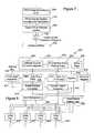
- the common configuration logic 228( FIG. 8 ) IIC interface 232 has a slave mode physical layer 800 and address decode and control registers 802 . These interface the IIC bus 226 to an internal, parallel, bus 804 . Two hundred fifty-six byte data-to-JTAG FIFO 806 and data-from-JTAG FIFO 808 are provided for buffering data transfers between the IIC and JTAG busses. Data can be transferred between IIC bus 226 and FIFOs 806 and 808 through IIC slave physical layer 800 .
- JTAG state machines 810enable single IIC commands to reset JTAG targets, read JTAG configuration, or transfer up to two hundred fifty six consecutive bytes between FIFOs 806 or 808 and a JTAG device through parallel-serial converter 812 or serial-parallel converter 814 according to the direction of the transfer.
- a simple bypass port 816allows for bypassing of the state machines 810 and FIFOs 806 and 808 in the event of logic error or need to perform unusual JTAG commands.
- Selection register 818is addressable through the IIC interface 232 .
- Selection register 818designates one of several JTAG ports 820 to be active at any time. This is done by instructing a multiplexor 822 to couple a specific data line from a JTAG port 820 to serial-parallel converter 814 ; and by designating which JTAG port 820 is to receive JTAG select lines from clock & select gating logic 824 .
- the common configuration logic 228also has a status register 826 , which includes error flags, FIFO dipsticks 900 and 902 (FIG. 9 ), FIFO empty flags 904 and 906 , and a configuration header connected flag 908 .
- the configuration header connected flag 908indicates whether any of the optional configuration headers, such as header 514 , is connected to a configuration system. If a configuration system is connected to a header 514 , the system management processor 526 identifies this when it checks 406 for a header connected, and will refuse to program EEPROMs to prevent accidental corruption of EEPROM contents.
- the FIFO empty flags 904 and 906are tested to ensure all transfers are complete when the system management subsystem processor 312 checks for errors 420 after writing code 418 to the EEPROMs
- the inventionhas been described with reference to a particular partitioning of functional elements among circuit boards of a computer system embodying the invention.
- the inventionis applicable to alternative partitionings of the system; there may be additional boards, or circuitry, illustrated as on separate boards, that may be combined, as necessary, for a particular embodiment.
- the common configuration logic illustrated as on Board E 230could be combined on a circuit board with the circuitry of Board D 204 .
Landscapes
- Engineering & Computer Science (AREA)
- Computer Hardware Design (AREA)
- Theoretical Computer Science (AREA)
- Physics & Mathematics (AREA)
- General Engineering & Computer Science (AREA)
- General Physics & Mathematics (AREA)
- Stored Programmes (AREA)
Abstract
Description
- 1. a configuration system must have knowledge of all devices in the chain in order to properly address any device on the chain; if a single chain is used the configuration system must have detailed knowledge of every board in the system.
- 2. large systems may, and often do, have slots permitting later addition or upgrade of peripheral devices, memory subsystems, processors, and other subsystems; additional circuitry would be required to avoid breaking a single chain at any empty slot.
- 3. large systems are often customized before shipment with a specific set of peripheral devices, memory subsystems, processors, and other devices; a single chain could require customized JTAG interface software for each system configuration.
- 4. access is faster to devices in short chains than to devices in long chains. A single board may, but need not, therefore embody more than one chain within the board.
Claims (8)
Priority Applications (3)
| Application Number | Priority Date | Filing Date | Title |
|---|---|---|---|
| US09/917,983US6918027B2 (en) | 2001-07-30 | 2001-07-30 | System and method for in-system programming through an on-system JTAG bridge of programmable logic devices on multiple circuit boards of a system |
| JP2002213352AJP2003058386A (en) | 2001-07-30 | 2002-07-23 | System and method for jtag bridge connection of programmable logic device on multiple circuit boards |
| EP02255295AEP1286355A3 (en) | 2001-07-30 | 2002-07-30 | System and method for in-system programming |
Applications Claiming Priority (1)
| Application Number | Priority Date | Filing Date | Title |
|---|---|---|---|
| US09/917,983US6918027B2 (en) | 2001-07-30 | 2001-07-30 | System and method for in-system programming through an on-system JTAG bridge of programmable logic devices on multiple circuit boards of a system |
Publications (2)
| Publication Number | Publication Date |
|---|---|
| US20030020512A1 US20030020512A1 (en) | 2003-01-30 |
| US6918027B2true US6918027B2 (en) | 2005-07-12 |
Family
ID=25439599
Family Applications (1)
| Application Number | Title | Priority Date | Filing Date |
|---|---|---|---|
| US09/917,983Expired - LifetimeUS6918027B2 (en) | 2001-07-30 | 2001-07-30 | System and method for in-system programming through an on-system JTAG bridge of programmable logic devices on multiple circuit boards of a system |
Country Status (3)
| Country | Link |
|---|---|
| US (1) | US6918027B2 (en) |
| EP (1) | EP1286355A3 (en) |
| JP (1) | JP2003058386A (en) |
Cited By (20)
| Publication number | Priority date | Publication date | Assignee | Title |
|---|---|---|---|---|
| US20030204807A1 (en)* | 2002-04-25 | 2003-10-30 | Tomofumi Watanabe | Data processor |
| US20040068330A1 (en)* | 2002-10-04 | 2004-04-08 | Ncr Corporation | Methods and apparatus for remote programming of field programmable gate arrays |
| US20040199748A1 (en)* | 2003-04-07 | 2004-10-07 | Zeev Sperber | Micro-operation un-lamination |
| US20050114473A1 (en)* | 2003-10-30 | 2005-05-26 | Ravid Guy | FPGA boot-up over a network |
| US20050246473A1 (en)* | 2004-04-28 | 2005-11-03 | Mehul Shah | Method for programming firmware hubs using service processors |
| US20060095731A1 (en)* | 2004-09-02 | 2006-05-04 | Yuval Bustan | Method and apparatus for avoiding read port assignment of a reorder buffer |
| US20060119384A1 (en)* | 2004-12-02 | 2006-06-08 | Altera Corporation | Techniques for combining volatile and non-volatile programmable logic on an integrated circuit |
| US20060212838A1 (en)* | 2005-02-09 | 2006-09-21 | Checksum, Llc | System and apparatus for in-system programming |
| US20070162972A1 (en)* | 2006-01-11 | 2007-07-12 | Sensory Networks, Inc. | Apparatus and method for processing of security capabilities through in-field upgrades |
| US7251804B1 (en) | 2004-10-01 | 2007-07-31 | Xilinx, Inc. | Structures and methods of overcoming localized defects in programmable integrated circuits by routing during the programming thereof |
| US7257654B1 (en)* | 2004-11-09 | 2007-08-14 | Advanced Micro Devices, Inc. | PCI bridge device configured for using JTAG scan for writing internal control registers and outputting debug state |
| US7284229B1 (en) | 2004-10-01 | 2007-10-16 | Xilinx, Inc. | Multiple bitstreams enabling the use of partially defective programmable integrated circuits while avoiding localized defects therein |
| US7287189B1 (en)* | 2003-06-25 | 2007-10-23 | Altera Corporation | I/O configuration and reconfiguration trigger through testing interface |
| US7412635B1 (en)* | 2004-10-01 | 2008-08-12 | Xilinx, Inc. | Utilizing multiple bitstreams to avoid localized defects in partially defective programmable integrated circuits |
| US7424655B1 (en) | 2004-10-01 | 2008-09-09 | Xilinx, Inc. | Utilizing multiple test bitstreams to avoid localized defects in partially defective programmable integrated circuits |
| US7619438B1 (en) | 2007-10-11 | 2009-11-17 | Xilinx, Inc. | Methods of enabling the use of a defective programmable device |
| US7810059B1 (en) | 2007-10-11 | 2010-10-05 | Xilinx, Inc. | Methods of enabling the validation of an integrated circuit adapted to receive one of a plurality of configuration bitstreams |
| US7853916B1 (en) | 2007-10-11 | 2010-12-14 | Xilinx, Inc. | Methods of using one of a plurality of configuration bitstreams for an integrated circuit |
| US8516176B1 (en) | 2012-10-11 | 2013-08-20 | Google Inc. | Gang programming of devices |
| US11100228B2 (en)* | 2018-10-25 | 2021-08-24 | Dell Products, L.P. | System and method to recover FPGA firmware over a sideband interface |
Families Citing this family (24)
| Publication number | Priority date | Publication date | Assignee | Title |
|---|---|---|---|---|
| US6678848B1 (en)* | 2000-12-21 | 2004-01-13 | Actel Corporation | Programming circuitry for configurable FPGA I/O |
| US6948147B1 (en)* | 2003-04-03 | 2005-09-20 | Xilinx, Inc. | Method and apparatus for configuring a programmable logic device using a master JTAG port |
| US7170315B2 (en) | 2003-07-31 | 2007-01-30 | Actel Corporation | Programmable system on a chip |
| US7190190B1 (en)* | 2004-01-09 | 2007-03-13 | Altera Corporation | Programmable logic device with on-chip nonvolatile user memory |
| US7019558B1 (en)* | 2004-07-14 | 2006-03-28 | Xilinx, Inc. | Conversion of configuration data to match communication protocol |
| DE602005021047D1 (en)* | 2005-01-21 | 2010-06-17 | Unltd Media Gmbh | A method of producing an impression of an audio signal |
| US7818584B1 (en) | 2005-01-25 | 2010-10-19 | Altera Corporation | One-time programmable memories for key storage |
| US7606362B1 (en) | 2005-01-25 | 2009-10-20 | Altera Corporation | FPGA configuration bitstream encryption using modified key |
| US20060242611A1 (en)* | 2005-04-07 | 2006-10-26 | Microsoft Corporation | Integrating programmable logic into personal computer (PC) architecture |
| GB2445303B (en)* | 2005-12-14 | 2008-08-20 | Dell Products Lp | System and method for configuring information handling system integrated circuits |
| US7693596B2 (en)* | 2005-12-14 | 2010-04-06 | Dell Products L.P. | System and method for configuring information handling system integrated circuits |
| US7636796B2 (en)* | 2006-09-15 | 2009-12-22 | Microsoft Corporation | Smart interconnect for modular multi-component embedded devices |
| US8712567B2 (en)* | 2006-12-22 | 2014-04-29 | Aviat U.S., Inc. | Manufactured product configuration |
| US8041444B2 (en) | 2006-12-22 | 2011-10-18 | Harris Stratex Networks Operating Corporation | Intelligent production station and production method |
| US7888965B2 (en)* | 2009-01-29 | 2011-02-15 | Texas Instruments Incorporated | Defining a default configuration for configurable circuitry in an integrated circuit |
| CN101621293B (en)* | 2009-07-23 | 2012-09-26 | 中兴通讯股份有限公司 | JTAG device and method for realizing JTAG data downloading through isolating circuit |
| CN102176128B (en)* | 2011-01-31 | 2012-10-31 | 黑龙江大学 | Two-stage interface combined MCU development board |
| CN102236572B (en)* | 2011-08-01 | 2013-10-09 | 华为技术有限公司 | A method and device for loading firmware |
| CN103577759B (en)* | 2012-08-09 | 2016-07-06 | 上海宝信软件股份有限公司 | A kind of data safe processing device based on non-security communication interface |
| DE102012217585B4 (en)* | 2012-09-27 | 2014-11-06 | Siemens Aktiengesellschaft | Method for automatic configuration of programmable devices, electronic assembly, x-ray detector and computed tomography system |
| US10089224B2 (en)* | 2013-03-15 | 2018-10-02 | The Boeing Company | Write caching using volatile shadow memory |
| CN104035803A (en)* | 2014-06-25 | 2014-09-10 | 浪潮(北京)电子信息产业有限公司 | Method, device and programmer for updating CPLD/FPGA firmware |
| US10331431B2 (en)* | 2015-11-17 | 2019-06-25 | Nlight, Inc. | Multiple laser module programming over internal communications bus of fiber laser |
| CN112416466B (en)* | 2020-12-02 | 2024-02-23 | 车智互联(北京)科技有限公司 | Application program loading method, mobile terminal and readable storage medium |
Citations (47)
| Publication number | Priority date | Publication date | Assignee | Title |
|---|---|---|---|---|
| US4914576A (en) | 1986-12-18 | 1990-04-03 | Bull Hn Information Systems Inc. | Apparatus and method of loading a control store memory of a central subsystem |
| US5101490A (en) | 1989-01-10 | 1992-03-31 | Bull Hn Information Systems Inc. | Peripheral device controller with an EEPROM with microinstructions for a RAM control store |
| US5343478A (en) | 1991-11-27 | 1994-08-30 | Ncr Corporation | Computer system configuration via test bus |
| US5425036A (en)* | 1992-09-18 | 1995-06-13 | Quickturn Design Systems, Inc. | Method and apparatus for debugging reconfigurable emulation systems |
| US5428800A (en)* | 1991-10-30 | 1995-06-27 | I-Cube, Inc. | Input/output (I/O) bidirectional buffer for interfacing I/O ports of a field programmable interconnection device with array ports of a cross-point switch |
| US5465056A (en)* | 1994-06-30 | 1995-11-07 | I-Cube, Inc. | Apparatus for programmable circuit and signal switching |
| US5477544A (en) | 1994-02-10 | 1995-12-19 | The United States Of America As Represented By The Secretary Of The Navy | Multi-port tester interface |
| US5761462A (en) | 1996-12-13 | 1998-06-02 | International Business Machines Corporation | Method and system for supporting peripheral component interconnect (PCI) peer-to-peer access across multiple PCI host bridges within a data-processing system |
| US5802268A (en) | 1994-11-22 | 1998-09-01 | Lucent Technologies Inc. | Digital processor with embedded eeprom memory |
| US5826048A (en) | 1997-01-31 | 1998-10-20 | Vlsi Technology, Inc. | PCI bus with reduced number of signals |
| US5864486A (en) | 1996-05-08 | 1999-01-26 | Lattice Semiconductor Corporation | Method and apparatus for in-system programming of a programmable logic device using a two-wire interface |
| US5894571A (en) | 1995-08-14 | 1999-04-13 | Dell U.S.A., L.P. | Process for configuring software in a build-to-order computer system |
| US5933614A (en) | 1996-12-31 | 1999-08-03 | Compaq Computer Corporation | Isolation of PCI and EISA masters by masking control and interrupt lines |
| US5935233A (en) | 1997-05-21 | 1999-08-10 | Micron Electronics, Inc. | Computer system with a switch interconnector for computer devices |
| US5970005A (en) | 1998-04-27 | 1999-10-19 | Ict, Inc. | Testing structure and method for high density PLDs which have flexible logic built-in blocks |
| US6031391A (en) | 1996-07-18 | 2000-02-29 | Altera Corporation | Configuration memory integrated circuit |
| US6044025A (en) | 1999-02-04 | 2000-03-28 | Xilinx, Inc. | PROM with built-in JTAG capability for configuring FPGAs |
| US6055632A (en) | 1997-09-25 | 2000-04-25 | Allen-Bradley Company, Llc | Method and apparatus for transferring firmware to a non-volatile memory of a programmable controller system |
| US6137738A (en) | 1999-11-30 | 2000-10-24 | Lucent Technologies, Inc. | Method for in-system programming of serially configured EEPROMS using a JTAG interface of a field programmable gate array |
| US6167358A (en) | 1997-12-19 | 2000-12-26 | Nowonder, Inc. | System and method for remotely monitoring a plurality of computer-based systems |
| US6167477A (en) | 1998-06-15 | 2000-12-26 | Sun Microsystems, Inc. | Computer system bridge employing a resource control mechanism with programmable registers to control resource allocation |
| US6198303B1 (en) | 1998-03-25 | 2001-03-06 | Altera Corporation | Configuration eprom with programmable logic |
| US6255849B1 (en) | 2000-02-04 | 2001-07-03 | Xilinx, Inc. | On-chip self-modification for PLDs |
| US6289406B1 (en) | 1998-11-06 | 2001-09-11 | Vlsi Technology, Inc. | Optimizing the performance of asynchronous bus bridges with dynamic transactions |
| US6314550B1 (en) | 1997-06-10 | 2001-11-06 | Altera Corporation | Cascaded programming with multiple-purpose pins |
| US6366973B1 (en) | 1999-05-03 | 2002-04-02 | 3Com Corporation | Slave interface circuit for providing communication between a peripheral component interconnect (PCI) domain and an advanced system bus (ASB) |
| US6401153B2 (en) | 1997-12-23 | 2002-06-04 | Intel Corporation | Mechanisms for converting interrupt request signals on address and data lines to interrupt message signals |
| US6405276B1 (en) | 1998-12-10 | 2002-06-11 | International Business Machines Corporation | Selectively flushing buffered transactions in a bus bridge |
| US20020070753A1 (en) | 1999-12-10 | 2002-06-13 | Diva Systems Corporation | Method and apparatus providing remote reprogramming of programmable logic devices using embedded JTAG physical layer and protocol |
| US6427198B1 (en) | 2000-02-15 | 2002-07-30 | International Business Machines Corporation | Method, system, and program for determining system configuration |
| US6430710B1 (en) | 1998-03-12 | 2002-08-06 | Hitachi, Ltd. | Data processing system with RAS data acquisition function |
| US6460108B1 (en) | 1999-03-31 | 2002-10-01 | Intel Corporation | Low cost data streaming mechanism |
| US6459297B1 (en) | 1999-09-20 | 2002-10-01 | Ag Communication Systems Corporation | System for programming field programmable devices |
| US6501682B2 (en) | 2000-07-12 | 2002-12-31 | Hitachi, Ltd. | Nonvolatile semiconductor memory device |
| US20030005207A1 (en) | 2001-06-29 | 2003-01-02 | Langendorf Brian K. | Virtual PCI device apparatus and method |
| US6526332B2 (en) | 2000-10-11 | 2003-02-25 | Sony Corporation | Robot control system and method for introducing robot control software |
| US6529989B1 (en) | 2000-05-03 | 2003-03-04 | Adaptec, Inc. | Intelligent expansion ROM sharing bus subsystem |
| US6567414B2 (en) | 1998-10-30 | 2003-05-20 | Intel Corporation | Method and apparatus for exiting a deadlock condition |
| US20030120974A1 (en) | 2000-09-14 | 2003-06-26 | Cadence Design Systems, Inc. | Programable multi-port memory bist with compact microcode |
| US6622206B1 (en) | 1999-06-11 | 2003-09-16 | International Business Machines Corporation | Method for controlling write cache transfer and disk unit |
| US6622246B1 (en) | 1999-11-12 | 2003-09-16 | Xerox Corporation | Method and apparatus for booting and upgrading firmware |
| US6629179B1 (en) | 2000-07-31 | 2003-09-30 | Adaptec, Inc. | Message signaled interrupt generating device and method |
| US6636927B1 (en) | 1999-09-24 | 2003-10-21 | Adaptec, Inc. | Bridge device for transferring data using master-specific prefetch sizes |
| US6651225B1 (en)* | 1997-05-02 | 2003-11-18 | Axis Systems, Inc. | Dynamic evaluation logic system and method |
| US6658508B1 (en) | 2000-01-31 | 2003-12-02 | Koninklijke Philips Electronics N.V. | Expansion module with external bus for personal digital assistant and design method therefor |
| US6658519B1 (en) | 2000-07-28 | 2003-12-02 | International Business Machines Corporation | Bus bridge with embedded input/output (I/O) and transaction tracing capabilities |
| US6691205B2 (en) | 2001-03-05 | 2004-02-10 | M-Systems Flash Disk Pioneers Ltd. | Method for using RAM buffers with simultaneous accesses in flash based storage systems |
- 2001
- 2001-07-30USUS09/917,983patent/US6918027B2/ennot_activeExpired - Lifetime
- 2002
- 2002-07-23JPJP2002213352Apatent/JP2003058386A/enactivePending
- 2002-07-30EPEP02255295Apatent/EP1286355A3/ennot_activeWithdrawn
Patent Citations (48)
| Publication number | Priority date | Publication date | Assignee | Title |
|---|---|---|---|---|
| US4914576A (en) | 1986-12-18 | 1990-04-03 | Bull Hn Information Systems Inc. | Apparatus and method of loading a control store memory of a central subsystem |
| US5101490A (en) | 1989-01-10 | 1992-03-31 | Bull Hn Information Systems Inc. | Peripheral device controller with an EEPROM with microinstructions for a RAM control store |
| US5428800A (en)* | 1991-10-30 | 1995-06-27 | I-Cube, Inc. | Input/output (I/O) bidirectional buffer for interfacing I/O ports of a field programmable interconnection device with array ports of a cross-point switch |
| US5343478A (en) | 1991-11-27 | 1994-08-30 | Ncr Corporation | Computer system configuration via test bus |
| US5425036A (en)* | 1992-09-18 | 1995-06-13 | Quickturn Design Systems, Inc. | Method and apparatus for debugging reconfigurable emulation systems |
| US5477544A (en) | 1994-02-10 | 1995-12-19 | The United States Of America As Represented By The Secretary Of The Navy | Multi-port tester interface |
| US5465056A (en)* | 1994-06-30 | 1995-11-07 | I-Cube, Inc. | Apparatus for programmable circuit and signal switching |
| US5802268A (en) | 1994-11-22 | 1998-09-01 | Lucent Technologies Inc. | Digital processor with embedded eeprom memory |
| US5894571A (en) | 1995-08-14 | 1999-04-13 | Dell U.S.A., L.P. | Process for configuring software in a build-to-order computer system |
| US5864486A (en) | 1996-05-08 | 1999-01-26 | Lattice Semiconductor Corporation | Method and apparatus for in-system programming of a programmable logic device using a two-wire interface |
| US6031391A (en) | 1996-07-18 | 2000-02-29 | Altera Corporation | Configuration memory integrated circuit |
| US6614259B2 (en) | 1996-07-18 | 2003-09-02 | Altera Corporation | Configuration memory integrated circuit |
| US5761462A (en) | 1996-12-13 | 1998-06-02 | International Business Machines Corporation | Method and system for supporting peripheral component interconnect (PCI) peer-to-peer access across multiple PCI host bridges within a data-processing system |
| US5933614A (en) | 1996-12-31 | 1999-08-03 | Compaq Computer Corporation | Isolation of PCI and EISA masters by masking control and interrupt lines |
| US5826048A (en) | 1997-01-31 | 1998-10-20 | Vlsi Technology, Inc. | PCI bus with reduced number of signals |
| US6651225B1 (en)* | 1997-05-02 | 2003-11-18 | Axis Systems, Inc. | Dynamic evaluation logic system and method |
| US5935233A (en) | 1997-05-21 | 1999-08-10 | Micron Electronics, Inc. | Computer system with a switch interconnector for computer devices |
| US6314550B1 (en) | 1997-06-10 | 2001-11-06 | Altera Corporation | Cascaded programming with multiple-purpose pins |
| US6055632A (en) | 1997-09-25 | 2000-04-25 | Allen-Bradley Company, Llc | Method and apparatus for transferring firmware to a non-volatile memory of a programmable controller system |
| US6167358A (en) | 1997-12-19 | 2000-12-26 | Nowonder, Inc. | System and method for remotely monitoring a plurality of computer-based systems |
| US6401153B2 (en) | 1997-12-23 | 2002-06-04 | Intel Corporation | Mechanisms for converting interrupt request signals on address and data lines to interrupt message signals |
| US6430710B1 (en) | 1998-03-12 | 2002-08-06 | Hitachi, Ltd. | Data processing system with RAS data acquisition function |
| US6198303B1 (en) | 1998-03-25 | 2001-03-06 | Altera Corporation | Configuration eprom with programmable logic |
| US5970005A (en) | 1998-04-27 | 1999-10-19 | Ict, Inc. | Testing structure and method for high density PLDs which have flexible logic built-in blocks |
| US6167477A (en) | 1998-06-15 | 2000-12-26 | Sun Microsystems, Inc. | Computer system bridge employing a resource control mechanism with programmable registers to control resource allocation |
| US6567414B2 (en) | 1998-10-30 | 2003-05-20 | Intel Corporation | Method and apparatus for exiting a deadlock condition |
| US6289406B1 (en) | 1998-11-06 | 2001-09-11 | Vlsi Technology, Inc. | Optimizing the performance of asynchronous bus bridges with dynamic transactions |
| US6405276B1 (en) | 1998-12-10 | 2002-06-11 | International Business Machines Corporation | Selectively flushing buffered transactions in a bus bridge |
| US6044025A (en) | 1999-02-04 | 2000-03-28 | Xilinx, Inc. | PROM with built-in JTAG capability for configuring FPGAs |
| US6460108B1 (en) | 1999-03-31 | 2002-10-01 | Intel Corporation | Low cost data streaming mechanism |
| US6366973B1 (en) | 1999-05-03 | 2002-04-02 | 3Com Corporation | Slave interface circuit for providing communication between a peripheral component interconnect (PCI) domain and an advanced system bus (ASB) |
| US6622206B1 (en) | 1999-06-11 | 2003-09-16 | International Business Machines Corporation | Method for controlling write cache transfer and disk unit |
| US6459297B1 (en) | 1999-09-20 | 2002-10-01 | Ag Communication Systems Corporation | System for programming field programmable devices |
| US6636927B1 (en) | 1999-09-24 | 2003-10-21 | Adaptec, Inc. | Bridge device for transferring data using master-specific prefetch sizes |
| US6622246B1 (en) | 1999-11-12 | 2003-09-16 | Xerox Corporation | Method and apparatus for booting and upgrading firmware |
| US6137738A (en) | 1999-11-30 | 2000-10-24 | Lucent Technologies, Inc. | Method for in-system programming of serially configured EEPROMS using a JTAG interface of a field programmable gate array |
| US20020070753A1 (en) | 1999-12-10 | 2002-06-13 | Diva Systems Corporation | Method and apparatus providing remote reprogramming of programmable logic devices using embedded JTAG physical layer and protocol |
| US6658508B1 (en) | 2000-01-31 | 2003-12-02 | Koninklijke Philips Electronics N.V. | Expansion module with external bus for personal digital assistant and design method therefor |
| US6255849B1 (en) | 2000-02-04 | 2001-07-03 | Xilinx, Inc. | On-chip self-modification for PLDs |
| US6427198B1 (en) | 2000-02-15 | 2002-07-30 | International Business Machines Corporation | Method, system, and program for determining system configuration |
| US6529989B1 (en) | 2000-05-03 | 2003-03-04 | Adaptec, Inc. | Intelligent expansion ROM sharing bus subsystem |
| US6501682B2 (en) | 2000-07-12 | 2002-12-31 | Hitachi, Ltd. | Nonvolatile semiconductor memory device |
| US6658519B1 (en) | 2000-07-28 | 2003-12-02 | International Business Machines Corporation | Bus bridge with embedded input/output (I/O) and transaction tracing capabilities |
| US6629179B1 (en) | 2000-07-31 | 2003-09-30 | Adaptec, Inc. | Message signaled interrupt generating device and method |
| US20030120974A1 (en) | 2000-09-14 | 2003-06-26 | Cadence Design Systems, Inc. | Programable multi-port memory bist with compact microcode |
| US6526332B2 (en) | 2000-10-11 | 2003-02-25 | Sony Corporation | Robot control system and method for introducing robot control software |
| US6691205B2 (en) | 2001-03-05 | 2004-02-10 | M-Systems Flash Disk Pioneers Ltd. | Method for using RAM buffers with simultaneous accesses in flash based storage systems |
| US20030005207A1 (en) | 2001-06-29 | 2003-01-02 | Langendorf Brian K. | Virtual PCI device apparatus and method |
Non-Patent Citations (4)
| Title |
|---|
| Beer, Iian, et al., "Establishing PCI Compliance Using Formal Verification: A Case Study," Mar. 28-31, 1995, IEEE 14th Annual International Phoenix Conference on Computers And Communications, p. 373-377. |
| Dehon, Andre, et al., "Reconfigurable Computing: What, Why And Implications For Design Automation," 1999, ACM Pres, p. 610-615. |
| Keahey, "Programming Of Flash With ICT Rights And Responsibilities", IEE, pp. 711-717, 2000. |
| XILINX: "XC18V00 Series Of In-System Programmable Configuration PROMs" DS026 (v2.8), Jun. 11, 2001, pp. 1-18. |
Cited By (32)
| Publication number | Priority date | Publication date | Assignee | Title |
|---|---|---|---|---|
| US7475325B2 (en) | 2002-04-25 | 2009-01-06 | Sanyo Electric Co., Ltd. | Data processor |
| US7020825B2 (en)* | 2002-04-25 | 2006-03-28 | Sanyo Electric Co., Ltd. | Data processor with serial transfer of control program |
| US20060085722A1 (en)* | 2002-04-25 | 2006-04-20 | Tomofumi Watanabe | Data processor |
| US20030204807A1 (en)* | 2002-04-25 | 2003-10-30 | Tomofumi Watanabe | Data processor |
| US20040068330A1 (en)* | 2002-10-04 | 2004-04-08 | Ncr Corporation | Methods and apparatus for remote programming of field programmable gate arrays |
| US20040199748A1 (en)* | 2003-04-07 | 2004-10-07 | Zeev Sperber | Micro-operation un-lamination |
| US7206921B2 (en)* | 2003-04-07 | 2007-04-17 | Intel Corporation | Micro-operation un-lamination |
| US7287189B1 (en)* | 2003-06-25 | 2007-10-23 | Altera Corporation | I/O configuration and reconfiguration trigger through testing interface |
| US20050114473A1 (en)* | 2003-10-30 | 2005-05-26 | Ravid Guy | FPGA boot-up over a network |
| US7136952B2 (en)* | 2004-04-28 | 2006-11-14 | International Business Machines Corporation | Method for programming firmware hubs using service processors |
| US20050246473A1 (en)* | 2004-04-28 | 2005-11-03 | Mehul Shah | Method for programming firmware hubs using service processors |
| US20060095731A1 (en)* | 2004-09-02 | 2006-05-04 | Yuval Bustan | Method and apparatus for avoiding read port assignment of a reorder buffer |
| US8117580B1 (en) | 2004-10-01 | 2012-02-14 | Xilinx, Inc. | Multiple bitstreams enabling the use of partially defective programmable integrated circuits while avoiding localized defects therein |
| US7849435B1 (en) | 2004-10-01 | 2010-12-07 | Xilinx, Inc. | Utilizing multiple test bitstreams to avoid localized defects in partially defective programmable integrated circuits |
| US7620863B1 (en) | 2004-10-01 | 2009-11-17 | Xilinx, Inc. | Utilizing multiple test bitstreams to avoid localized defects in partially defective programmable integrated circuits |
| US7251804B1 (en) | 2004-10-01 | 2007-07-31 | Xilinx, Inc. | Structures and methods of overcoming localized defects in programmable integrated circuits by routing during the programming thereof |
| US7284229B1 (en) | 2004-10-01 | 2007-10-16 | Xilinx, Inc. | Multiple bitstreams enabling the use of partially defective programmable integrated circuits while avoiding localized defects therein |
| US7412635B1 (en)* | 2004-10-01 | 2008-08-12 | Xilinx, Inc. | Utilizing multiple bitstreams to avoid localized defects in partially defective programmable integrated circuits |
| US7424655B1 (en) | 2004-10-01 | 2008-09-09 | Xilinx, Inc. | Utilizing multiple test bitstreams to avoid localized defects in partially defective programmable integrated circuits |
| US7257654B1 (en)* | 2004-11-09 | 2007-08-14 | Advanced Micro Devices, Inc. | PCI bridge device configured for using JTAG scan for writing internal control registers and outputting debug state |
| US20060119384A1 (en)* | 2004-12-02 | 2006-06-08 | Altera Corporation | Techniques for combining volatile and non-volatile programmable logic on an integrated circuit |
| US7242218B2 (en)* | 2004-12-02 | 2007-07-10 | Altera Corporation | Techniques for combining volatile and non-volatile programmable logic on an integrated circuit |
| US20090138841A1 (en)* | 2005-02-09 | 2009-05-28 | Checksum, Llc | System and apparatus for in-system programming |
| US7802021B2 (en) | 2005-02-09 | 2010-09-21 | Checksum, Llc | System and apparatus for in-system programming |
| US20060212838A1 (en)* | 2005-02-09 | 2006-09-21 | Checksum, Llc | System and apparatus for in-system programming |
| US20070162972A1 (en)* | 2006-01-11 | 2007-07-12 | Sensory Networks, Inc. | Apparatus and method for processing of security capabilities through in-field upgrades |
| US7619438B1 (en) | 2007-10-11 | 2009-11-17 | Xilinx, Inc. | Methods of enabling the use of a defective programmable device |
| US7810059B1 (en) | 2007-10-11 | 2010-10-05 | Xilinx, Inc. | Methods of enabling the validation of an integrated circuit adapted to receive one of a plurality of configuration bitstreams |
| US7853916B1 (en) | 2007-10-11 | 2010-12-14 | Xilinx, Inc. | Methods of using one of a plurality of configuration bitstreams for an integrated circuit |
| US8516176B1 (en) | 2012-10-11 | 2013-08-20 | Google Inc. | Gang programming of devices |
| US8825934B2 (en) | 2012-10-11 | 2014-09-02 | Google Inc. | Gang programming of devices |
| US11100228B2 (en)* | 2018-10-25 | 2021-08-24 | Dell Products, L.P. | System and method to recover FPGA firmware over a sideband interface |
Also Published As
| Publication number | Publication date |
|---|---|
| EP1286355A2 (en) | 2003-02-26 |
| US20030020512A1 (en) | 2003-01-30 |
| EP1286355A3 (en) | 2004-05-06 |
| JP2003058386A (en) | 2003-02-28 |
Similar Documents
| Publication | Publication Date | Title |
|---|---|---|
| US6918027B2 (en) | System and method for in-system programming through an on-system JTAG bridge of programmable logic devices on multiple circuit boards of a system | |
| US6883109B2 (en) | Method for accessing scan chains and updating EEPROM-resident FPGA code through a system management processor and JTAG bus | |
| CN107493685B (en) | Reprogramming a port controller via its own external port | |
| US20040225783A1 (en) | Bus to multiple jtag bus bridge | |
| US7676694B2 (en) | Managing system components | |
| US6463550B1 (en) | Computer system implementing fault detection and isolation using unique identification codes stored in non-volatile memory | |
| US5805882A (en) | Computer system and method for replacing obsolete or corrupt boot code contained within reprogrammable memory with new boot code supplied from an external source through a data port | |
| US5878256A (en) | Method and apparatus for providing updated firmware in a data processing system | |
| US8943302B2 (en) | Method of flashing bios using service processor and computer system using the same | |
| US4794558A (en) | Microprocessor having self-programmed eprom | |
| US20030023793A1 (en) | Method and apparatus for in-system programming through a common connection point of programmable logic devices on multiple circuit boards of a system | |
| CN103477296A (en) | Apparatus for configuring a programmable logic device from a BIOS PROM | |
| JPH0863340A (en) | Method and equipment for communication of configuration information of system in network | |
| US9946552B2 (en) | System and method for detecting redundant array of independent disks (RAID) controller state from baseboard management controller (BMC) | |
| CN115344308A (en) | Safe boot device and method | |
| US7080164B2 (en) | Peripheral device having a programmable identification configuration register | |
| EP0029855B1 (en) | Microcomputer with mpu-programmable eprom | |
| US11334359B2 (en) | Systems and methods for management of dynamic devices | |
| WO2000025208A1 (en) | Processor system with fail safe bios configuration | |
| Trujilho et al. | Dependable I2C communication with FPGA | |
| US6865693B1 (en) | System and method for debugging multiprocessor systems | |
| US7089358B2 (en) | Identifying and controlling different types of MROMB hardware | |
| CA2392503A1 (en) | Computer module and motherboard | |
| CN120803547A (en) | FPGA configuration method, system and storage medium | |
| GB2356715A (en) | Single board computer module |
Legal Events
| Date | Code | Title | Description |
|---|---|---|---|
| AS | Assignment | Owner name:HEWLETT-PACKARD COMPANY, COLORADO Free format text:ASSIGNMENT OF ASSIGNORS INTEREST;ASSIGNORS:MANTEY, PAUL;ERICKSON, MIKE;MACIOROWSKI, DAVID;REEL/FRAME:012491/0916;SIGNING DATES FROM 20010717 TO 20010723 | |
| AS | Assignment | Owner name:HEWLETT-PACKARD DEVELOPMENT COMPANY L.P., TEXAS Free format text:ASSIGNMENT OF ASSIGNORS INTEREST;ASSIGNOR:HEWLETT-PACKARD COMPANY;REEL/FRAME:014061/0492 Effective date:20030926 Owner name:HEWLETT-PACKARD DEVELOPMENT COMPANY L.P.,TEXAS Free format text:ASSIGNMENT OF ASSIGNORS INTEREST;ASSIGNOR:HEWLETT-PACKARD COMPANY;REEL/FRAME:014061/0492 Effective date:20030926 | |
| STCF | Information on status: patent grant | Free format text:PATENTED CASE | |
| FPAY | Fee payment | Year of fee payment:4 | |
| REMI | Maintenance fee reminder mailed | ||
| FPAY | Fee payment | Year of fee payment:8 | |
| SULP | Surcharge for late payment | Year of fee payment:7 | |
| AS | Assignment | Owner name:HEWLETT PACKARD ENTERPRISE DEVELOPMENT LP, TEXAS Free format text:ASSIGNMENT OF ASSIGNORS INTEREST;ASSIGNOR:HEWLETT-PACKARD DEVELOPMENT COMPANY, L.P.;REEL/FRAME:037079/0001 Effective date:20151027 | |
| REMI | Maintenance fee reminder mailed | ||
| FPAY | Fee payment | Year of fee payment:12 | |
| SULP | Surcharge for late payment | Year of fee payment:11 | |
| AS | Assignment | Owner name:VALTRUS INNOVATIONS LIMITED, IRELAND Free format text:ASSIGNMENT OF ASSIGNORS INTEREST;ASSIGNOR:OT PATENT ESCROW, LLC;REEL/FRAME:060005/0600 Effective date:20220504 |