US6916728B2 - Method for forming a semiconductor structure through epitaxial growth - Google Patents
Method for forming a semiconductor structure through epitaxial growthDownload PDFInfo
- Publication number
- US6916728B2 US6916728B2US10/328,923US32892302AUS6916728B2US 6916728 B2US6916728 B2US 6916728B2US 32892302 AUS32892302 AUS 32892302AUS 6916728 B2US6916728 B2US 6916728B2
- Authority
- US
- United States
- Prior art keywords
- layer
- dielectric material
- semiconductor
- semiconductor layer
- anchor portion
- Prior art date
- Legal status (The legal status is an assumption and is not a legal conclusion. Google has not performed a legal analysis and makes no representation as to the accuracy of the status listed.)
- Expired - Lifetime
Links
Images


Classifications
- B—PERFORMING OPERATIONS; TRANSPORTING
- B81—MICROSTRUCTURAL TECHNOLOGY
- B81C—PROCESSES OR APPARATUS SPECIALLY ADAPTED FOR THE MANUFACTURE OR TREATMENT OF MICROSTRUCTURAL DEVICES OR SYSTEMS
- B81C1/00—Manufacture or treatment of devices or systems in or on a substrate
- B81C1/00436—Shaping materials, i.e. techniques for structuring the substrate or the layers on the substrate
- B81C1/00444—Surface micromachining, i.e. structuring layers on the substrate
- B81C1/00468—Releasing structures
- B81C1/00476—Releasing structures removing a sacrificial layer
- B—PERFORMING OPERATIONS; TRANSPORTING
- B81—MICROSTRUCTURAL TECHNOLOGY
- B81B—MICROSTRUCTURAL DEVICES OR SYSTEMS, e.g. MICROMECHANICAL DEVICES
- B81B2201/00—Specific applications of microelectromechanical systems
- B81B2201/02—Sensors
- B81B2201/0228—Inertial sensors
- B81B2201/025—Inertial sensors not provided for in B81B2201/0235 - B81B2201/0242
- B—PERFORMING OPERATIONS; TRANSPORTING
- B81—MICROSTRUCTURAL TECHNOLOGY
- B81B—MICROSTRUCTURAL DEVICES OR SYSTEMS, e.g. MICROMECHANICAL DEVICES
- B81B2203/00—Basic microelectromechanical structures
- B81B2203/03—Static structures
- B81B2203/0307—Anchors
- B—PERFORMING OPERATIONS; TRANSPORTING
- B81—MICROSTRUCTURAL TECHNOLOGY
- B81C—PROCESSES OR APPARATUS SPECIALLY ADAPTED FOR THE MANUFACTURE OR TREATMENT OF MICROSTRUCTURAL DEVICES OR SYSTEMS
- B81C2201/00—Manufacture or treatment of microstructural devices or systems
- B81C2201/01—Manufacture or treatment of microstructural devices or systems in or on a substrate
- B81C2201/0101—Shaping material; Structuring the bulk substrate or layers on the substrate; Film patterning
- B81C2201/0102—Surface micromachining
- B81C2201/0105—Sacrificial layer
- B81C2201/0109—Sacrificial layers not provided for in B81C2201/0107 - B81C2201/0108
- Y—GENERAL TAGGING OF NEW TECHNOLOGICAL DEVELOPMENTS; GENERAL TAGGING OF CROSS-SECTIONAL TECHNOLOGIES SPANNING OVER SEVERAL SECTIONS OF THE IPC; TECHNICAL SUBJECTS COVERED BY FORMER USPC CROSS-REFERENCE ART COLLECTIONS [XRACs] AND DIGESTS
- Y10—TECHNICAL SUBJECTS COVERED BY FORMER USPC
- Y10S—TECHNICAL SUBJECTS COVERED BY FORMER USPC CROSS-REFERENCE ART COLLECTIONS [XRACs] AND DIGESTS
- Y10S438/00—Semiconductor device manufacturing: process
- Y10S438/977—Thinning or removal of substrate
Definitions
- the present inventionrelates generally to microfabrication techniques, and more particularly to methods for making semiconductor structures such as MEMS devices.
- MEMSMicroElectroMechanical Systems
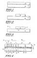
- FIGS. 1-3illustrate a conventional method for creating a MEMS structure on an SOI wafer.
- a silicon wafer substrate 15is provided having a silicon dioxide sacrificial layer 13 disposed thereon.
- a layer of active single crystal silicon 11is disposed over the sacrificial layer.
- the layer of active single-crystal siliconis then masked, patterned and selectively etched to yield the structure shown in FIG. 2 , after which the sacrificial layer is partially removed by selective chemical etching to release the structure.
- the released MEMS structure 12has a cantilevered portion 17 formed of Si and an anchor portion 19 formed of SiO 2 .
- a second trenchis created exterior to the first trench which extends through at least the silicon layer and exposes at least a portion of the second region of the sacrificial layer.
- the second region of the sacrificial layeris then contacted, by way of the second trench, with a chemical etching solution which is adapted to etch the sacrificial layer and which is selective to the first material. Since the material disposed in the first trench acts as a barrier to the etch, the timing of the etch is no longer critical, and MEMS structures may be produced through this approach which have anchor portions that do not vary significantly from one batch to another. Consequently, the anchor perimeter can be minimized, thereby minimizing parasitic capacitance and resulting in a reduction in die size.
- O'Brien et al.relies on deep reactive ion etching (RIE) of both the device silicon and the sacrificial layer to form the anchor portion of the device.
- RIEdeep reactive ion etching
- the etch rate of the sacrificial layer at the bottom of a deep and narrow trench extending all the way through the device layeris rather slow.
- a wet etchcould be used to etch the portion of the sacrificial layer at the bottom of the trench, the undercut typically caused by such an etch would result in undesirable void formation in the anchor area during backfill of the trench.
- the approach of O'Brien et al.also results in a device in which the anchor material is a different material than the single crystal silicon used in the device layer, which makes it more difficult to integrate with CMOS devices and other such structures.
- the present inventionrelates to a method for creating a semiconductor structure such as a MEMS structure.
- an articlewhich comprises a substrate and a single crystal semiconductor layer (such as, for example, single crystal silicon) and which has a sacrificial layer comprising a first dielectric material disposed between the substrate and the semiconductor layer.
- An openingis created which extends through the semiconductor layer and the sacrificial layer and which exposes a portion of the substrate.
- An anchor portionis then formed in the opening.
- the anchor portioncomprises a second dielectric material, and may comprise at least a first and second layer, wherein the first layer comprises the second dielectric material, and wherein the second layer comprises a material which is preferably conductive, such as polysilicon.
- the second dielectric materialis preferably silicon nitride, and even more preferably silicon rich silicon nitride, and is preferably diverse from the first dielectric material.
- the step of forming the anchor portionmay comprise the steps of depositing the second dielectric material over the semiconductor layer such that the opening is filled, and etching the second dielectric material down to the semiconductor layer.
- the semiconductor layeris then epitaxially grown to a suitable device thickness, thereby forming a device layer.
- the device layerpreferably covers the anchor portion, and the surface of the device layer preferably comprises single crystal silicon.
- the methodmay further comprise the steps of forming a semiconductor structure from the device layer, and removing at least a portion of the sacrificial layer, thereby releasing the semiconductor structure.
- the step of removing at least a portion of the sacrificial layermay include the steps of creating a second opening which exposes a portion of the sacrificial layer, and contacting the sacrificial layer, by way of the second opening, with an etchant (such as an aqueous solution of HF) which is selective to the material of the anchor portion.
- the released semiconductor structuremay be a MEMS structure, and may comprise an anchor area, a proof mass area, a moving finger, and a fixed finger.
- a method for creating a semiconductor structuresuch as a MEMS structure.
- an articlewhich comprises a substrate and a single crystal semiconductor layer and which has a sacrificial layer comprising a first dielectric material which is disposed between the substrate and the semiconductor layer.
- An anchor portionis then formed which comprises a second dielectric material.
- the second dielectric materialis preferably silicon nitride, and even more preferably is silicon rich silicon nitride.
- the anchor portionis in contact with the substrate and extends through the semiconductor layer and the sacrificial layer.
- the semiconductor layeris then epitaxially grown to a suitable device thickness, thereby forming a device layer.
- the device layerpreferably covers the anchor portion and has a surface which comprises single crystal silicon.
- a semiconductor structureis then formed in the device layer, and at least a portion of the sacrificial layer is removed with an etchant.
- the etchantwhich may comprise an aqueous HF solution, is preferably selective to the second dielectric material.
- a method for creating a semiconductor structuresuch as a MEMS structure.
- an articlewhich comprises a substrate and a single crystal semiconductor layer and which has a sacrificial layer comprising a dielectric material which is disposed between the substrate and the semiconductor layer.
- a first trenchis created which extends through the semiconductor layer and the sacrificial layer.
- Silicon nitrideis then deposited into the first trench, and a semiconductor structure is formed in the semiconductor layer.
- a second trenchis then created which contacts the sacrificial layer, and the sacrificial layer is contacted by way of the second trench with a solution that etches the sacrificial layer and that is selective to silicon nitride and to the semiconductor layer.
- an inertial sensorin yet another aspect, includes an anchor comprising a base having at least one support structure depending therefrom which is in contact with the substrate.
- the support structurecomprises silicon nitride, and may comprise a plurality of concentric walls comprising silicon nitride, the walls having a portion of silicon oxide disposed between them.
- the portion of the base directly overlying the support structurecomprises single crystal silicon.
- the sensorhas a proof mass supported by the anchor portion, and the proof mass has a first set of spaced-apart, elongated fingers projecting therefrom.
- the sensoralso includes a second set of spaced-apart, elongated fingers, and further includes a spring which connects the proof mass to the base of the anchor such that the first and second set of fingers interdigitate.
- FIGS. 1-3are illustrations of a prior art method for making a MEMS structure
- FIG. 4is an illustration of a MEMS device made in accordance with the teachings herein;
- FIGS. 5-10are illustrations depicting the methodology used to achieve the device of FIG. 4 ;
- FIG. 11is an illustration of a MEMS device made in accordance with the teachings herein.
- epitaxy growthrefers to a process whereby an article is placed in a reactor and subjected to conditions in which single crystal silicon will grow on any exposed single crystal surfaces of the device. The process may also result in the growth, at least initially, of polycrystalline silicon on exposed surfaces of the device which are polycrystalline in nature.
- an anchor portion of a MEMS device or other semiconductor structuremay be formed without the need for reactive ion etching of the sacrificial layer at the bottom of a trench extending through the device layer thickness. This may be accomplished by forming the part of the anchor portion that extends through the sacrificial layer, before total device layer thickness is achieved.
- the anchor portionmay be at least partially formed in an SOI wafer comprising a substrate and a thin single crystal semiconductor layer and having a sacrificial layer comprising a first dielectric material disposed between the substrate and the semiconductor layer. After the anchor portion is formed, the thin single crystal semiconductor layer may be grown to the desired device thickness.
- a MEMS device or other semiconductor structuremay be formed on a substrate, and particularly from an SOI wafer, such that the perimeter of the anchor portion of the structure (and hence the wafer size) can be minimized, is not affected by variations in etch rates, and does not vary significantly from one product batch to another, by protecting the anchor portion during release by one or more materials which are resistant to the etch used to achieve release of the structure.
- SOI devicefor example, this may be accomplished by forming the anchor portion of the structure at least partially out of an anchor material such as silicon nitride, and then releasing the structure with a release agent, such as an aqueous solution of HF, that is selective to the anchor material.
- anchor sizeis not affected by variations in etch rates, and does not vary significantly from one product batch to another. Consequently, there is no need to factor variations in etch rates into the anchor size. Therefore, anchor size may be minimized, thus reducing the overall size of the device.
- the reduction in anchor sizealso has the benefit of reducing parasitic capacitance.
- FIGS. 4-10The methodologies described herein may be understood with reference to FIGS. 4-10 .
- the devicedepicted in these figuresis a hypothetical MEMS device, the relevant features of which have been consolidated into a single cross-section so that the effect of each processing step on these features will be evident from a single figure. It is to be understood, however, that in an actual MEMS device, these features may not all appear in any single cross-section of the device.
- FIG. 11illustrates a design for an actual MEMS device that may be made in accordance with the methodologies described herein.
- FIG. 4illustrates a MEMS device 51 made in accordance with the teachings herein.
- the deviceis created on a substrate comprising a silicon wafer 53 , a sacrificial layer 55 and a single crystal semiconductor layer 57 , and has an anchor portion 59 and a suspended portion 61 .
- the anchor portion in the particular device depictedis equipped with a plurality of nitride anchors 63 .
- the devicehas an epitaxially grown device layer 65 which is epitaxial polysilicon in the areas 67 over the nitride anchors, and which is single crystal silicon 69 elsewhere.
- the area 67may also consist essentially of single crystal silicon if the epitaxial overgrowth is made to occur laterally. This may occur, for example, if the rate of growth of single crystal silicon growing vertically and laterally from the portions of the semiconductor layer 105 adjacent to the nitride anchors 109 is greater than the rate of growth of polysilicon growing vertically from the nitride anchors 109 . It is desirable for the area 67 to be single crystal silicon because the resulting surface will typically be planar. By contrast, if the polysilicon in the areas over the nitride anchors is allowed to grow to the surface of the device layer, a non-planar surface may result. A non-planar surface is undesirable in that the fine line lithography commonly used to develop surface features on the device has limited depth focus.
- the deviceis equipped with a proof mass area 71 , at least one moving finger 73 , at least one fixed finger 75 , and a spring suspension 77 . Release of the structure is accomplished through the creation of horizontal trench 79 by introducing an etchant into vertical trenches 81 , 83 , 85 , 87 , 89 , 91 , 93 and 95 .
- FIGS. 5-10illustrate the methodology used to achieve the structure depicted in FIG. 4 .
- the processbegins with an SOI wafer 101 which has a silicon dioxide sacrificial layer 103 disposed thereon, and a thin semiconductor layer 105 , preferably comprising active single-crystalline silicon, disposed on the buried oxide layer.
- the thin semiconductor layeris preferably less than 10 microns thick, more preferably less than 7 microns thick, and most preferably within the range of about 0.1 to about 0.5 microns thick.
- a thin oxide layer(not shown) may be disposed on top of the semiconductor layer 105 .
- the waferis then patterned and etched as shown in FIG.
- the etching used to define the trenches 107is typically a reactive ion etch (RIE) and is carefully controlled to achieve trenches having openings of predetermined size.
- RIEreactive ion etch
- a layer of anchor material 109is then deposited over the structure.
- the thickness of the anchor materialis controlled to completely fill the trenches.
- the use of silicon rich silicon nitride as the anchor materialis advantageous herein because this material has very low stress.
- relatively thick layers (about 1 micron) of silicon rich silicon nitridecan be deposited, if so desired, without cracking or delamination.
- silicon rich silicon nitridehas a very low etch rate, compared to that of typical sacrificial oxide layers, in HF solutions (about 80 ⁇ /min in 49% HF solutions) commonly used to release MEMS structures on SOI wafers.
- the amount of undercut of the nitride anchoris very small compared to the undercut of the sacrificial layer.
- the anchor materialmay be deposited as at least a first and second layer, wherein the first layer comprises a first material such as silicon nitride, and wherein the second layer comprises a second material, such as polysilicon, which is diverse from the first material.
- the layer of anchor material 109is then etched down to the semiconductor layer 105 .
- the etch used in this stepis preferably either a wet etch or a partial RIE. If a partial RIE is used, it is preferably followed by a wet etch so as to minimize damage to the semiconductor layer.
- a thin oxide layermay be added to the top of the semiconductor layer in the structure of FIG. 6 prior to the formation of the trenches 107 therein, and this thin oxide layer may be used as an etch stop in the etch used to remove the layer of anchor material 109 in FIG. 8 .
- the thin oxide layermay then be stripped with a wet etch, thus avoiding any damage to the underlying semiconductor layer 105 .
- a layer of silicon 111is epitaxially grown over the device to the desired device thickness.
- the anchor material 109seeds the growth of polysilicon
- the underlying semiconductor layer 105seeds the growth of single crystal silicon.
- the layer of silicon over the anchor portionmay also be grown as single crystal silicon if the epitaxial overgrowth is made to occur laterally from portions of the semiconductor layer 105 adjacent to the anchor material at a faster rate than the epitaxial growth of polysilicon seeded by the anchor material 109 .
- FIG. 10depicts the completed structure prior to release.
- Deep RIEis used to create a series of trenches 117 , 119 , 121 , 123 , 125 , 127 , 129 , and 131 which extend down to the sacrificial layer 103 and which define the anchor portion 133 and the suspended portion 135 of the device.
- the suspended portion of the deviceconsists of a spring suspension 137 and a proof mass area 143 .
- the fixed finger 139 and the moving finger 141may also be released. Release of the structure may then be achieved through an oxide etch of the sacrificial layer to achieve the structure shown in FIG. 4 . This oxide etch may be achieved, for example, with an aqueous HF solution. Since the anchor material is chosen to be resistant to the oxide etch, the perimeter of the anchor portion of the structure (and hence the wafer size) can be minimized, is not affected by variations in etch rates, and does not vary significantly from one product batch to another.
- FIG. 11illustrates one possible design for a MEMS device (in this case, an accelerometer) that can be made using the methodologies described herein, it being understood that a wide variety of other designs and devices are achievable with these methodologies.
- the device 200has a proof mass area 203 with a suspended portion 205 and an anchored portion 207 .
- the anchored portionis attached to a substrate (not shown) by a plurality of proof mass anchors 209 .
- the suspended portionhas a plurality of etch holes 211 therein and is equipped with a plurality of moving fingers 213 .
- Each of the moving fingersis disposed between first 215 and second 217 fixed fingers, which are anchored by first 219 and second 221 sets of anchor fingers, respectively.
- a spring 223is disposed between the suspended portion and the anchored portion of the device.
- etchantsmay be used in the methodologies described herein. The choice of etchants will depend on various factors, such as the composition of the substrate, sacrificial layer or semiconductor layer, the composition of components or features present on the article at the time of etch, and the selectivity of a prospective etch.
- the etchantis an aqueous HF solution, although the etchant may also be HF with various concentrations of acetic acid. These materials may be used as aqueous or organic solvent based solutions, and the solutions may be buffered. In some applications, vapor phase HF may also be used to effect release of the semiconductor structure.
- Methodshave been provided herein for producing a MEMS structure on a substrate, and particularly on an SOI wafer, in which the suspended portion of the structure is protected during release by one or more materials which are resistant to the etch used to achieve release of the structure.
- the anchor portion of the structuremay likewise comprise one or more materials which are resistant to the etch used to achieve release of the structure.
Landscapes
- Engineering & Computer Science (AREA)
- Manufacturing & Machinery (AREA)
- Microelectronics & Electronic Packaging (AREA)
- Micromachines (AREA)
- Pressure Sensors (AREA)
Abstract
Description
Claims (41)
Priority Applications (1)
| Application Number | Priority Date | Filing Date | Title |
|---|---|---|---|
| US10/328,923US6916728B2 (en) | 2002-12-23 | 2002-12-23 | Method for forming a semiconductor structure through epitaxial growth |
Applications Claiming Priority (1)
| Application Number | Priority Date | Filing Date | Title |
|---|---|---|---|
| US10/328,923US6916728B2 (en) | 2002-12-23 | 2002-12-23 | Method for forming a semiconductor structure through epitaxial growth |
Publications (2)
| Publication Number | Publication Date |
|---|---|
| US20040119125A1 US20040119125A1 (en) | 2004-06-24 |
| US6916728B2true US6916728B2 (en) | 2005-07-12 |
Family
ID=32594622
Family Applications (1)
| Application Number | Title | Priority Date | Filing Date |
|---|---|---|---|
| US10/328,923Expired - LifetimeUS6916728B2 (en) | 2002-12-23 | 2002-12-23 | Method for forming a semiconductor structure through epitaxial growth |
Country Status (1)
| Country | Link |
|---|---|
| US (1) | US6916728B2 (en) |
Cited By (8)
| Publication number | Priority date | Publication date | Assignee | Title |
|---|---|---|---|---|
| US20060081929A1 (en)* | 2004-10-20 | 2006-04-20 | Samsung Electronics Co., Ltd. | Silicon-on-insulator substrate, fabricating method thereof, and method for fabricating floating structure using the same |
| US20060207968A1 (en)* | 2005-03-08 | 2006-09-21 | Mumbauer Paul D | Selective etching of oxides from substrates |
| US20060281214A1 (en)* | 2005-06-13 | 2006-12-14 | Chilcott Dan W | Method of making a soi silicon structure |
| US7531424B1 (en)* | 2005-05-03 | 2009-05-12 | Discera, Inc. | Vacuum wafer-level packaging for SOI-MEMS devices |
| EP2138453A1 (en) | 2008-06-23 | 2009-12-30 | Commissariat a L'Energie Atomique | Method for manufacturing an electromechanical structure comprising at least one mechanical reinforcement post |
| US20100233882A1 (en)* | 2009-03-11 | 2010-09-16 | Honeywell International Inc. | Single silicon-on-insulator (soi) wafer accelerometer fabrication |
| US8648432B2 (en)* | 2011-11-28 | 2014-02-11 | Texas Instruments Deutschland Gmbh | Fully embedded micromechanical device, system on chip and method for manufacturing the same |
| CN104609359A (en)* | 2013-11-05 | 2015-05-13 | 中芯国际集成电路制造(上海)有限公司 | Method for forming capacitance MEMS inertial sensor |
Families Citing this family (11)
| Publication number | Priority date | Publication date | Assignee | Title |
|---|---|---|---|---|
| US7585744B2 (en)* | 2003-12-08 | 2009-09-08 | Freescale Semiconductor, Inc. | Method of forming a seal for a semiconductor device |
| US7288464B2 (en) | 2005-04-11 | 2007-10-30 | Hewlett-Packard Development Company, L.P. | MEMS packaging structure and methods |
| US20060234412A1 (en)* | 2005-04-19 | 2006-10-19 | Hewlett-Packard Development Company, L.P. Intellectual Property Administration | MEMS release methods |
| FR2923475B1 (en)* | 2007-11-09 | 2009-12-18 | Commissariat Energie Atomique | METHOD FOR MAKING A SUSPENDED MEMBRANE DEVICE |
| WO2009125422A1 (en)* | 2008-04-11 | 2009-10-15 | Indian Institute Of Science | A sub-threshold forced plate fet sensor for sensing inertial displacements, a method and system thereof |
| TWI360516B (en)* | 2008-05-09 | 2012-03-21 | Pixart Imaging Inc | In-plane sensor and method for making same |
| US9735062B1 (en)* | 2016-06-03 | 2017-08-15 | International Business Machines Corporation | Defect reduction in channel silicon germanium on patterned silicon |
| US10167191B2 (en)* | 2017-04-04 | 2019-01-01 | Kionix, Inc. | Method for manufacturing a micro electro-mechanical system |
| US11180366B2 (en)* | 2020-03-23 | 2021-11-23 | General Electric Company | Methods for forming a MEMS device layer on an active device layer and devices formed thereby |
| DE102020114347B3 (en)* | 2020-05-28 | 2021-10-28 | Infineon Technologies Ag | MEMS devices with spring element and comb drive and related manufacturing processes |
| US11661337B2 (en)* | 2020-10-19 | 2023-05-30 | Taiwan Semiconductor Manufacturing Company, Ltd. | Comb electrode release process for MEMS structure |
Citations (12)
| Publication number | Priority date | Publication date | Assignee | Title |
|---|---|---|---|---|
| US5258097A (en) | 1992-11-12 | 1993-11-02 | Ford Motor Company | Dry-release method for sacrificial layer microstructure fabrication |
| US5310450A (en) | 1991-07-06 | 1994-05-10 | Robert Bosch Gmbh | Method of making an acceleration sensor |
| US5576250A (en) | 1992-12-28 | 1996-11-19 | Commissariat A L'energie Atomique | Process for the production of accelerometers using silicon on insulator technology |
| US5616514A (en) | 1993-06-03 | 1997-04-01 | Robert Bosch Gmbh | Method of fabricating a micromechanical sensor |
| US5616523A (en) | 1993-05-06 | 1997-04-01 | Robert Bosch Gmbh | Method of manufacturing sensor |
| US5750420A (en) | 1995-07-21 | 1998-05-12 | Commissariat A L'energie Atomique | Method for manufacturing a structure with a useful layer held at a distance from a substrate by abutments, and for detaching such a layer |
| US5937275A (en) | 1995-07-21 | 1999-08-10 | Robert Bosch Gmbh | Method of producing acceleration sensors |
| US5959208A (en) | 1995-02-08 | 1999-09-28 | Robert Bosch GmbH | Acceleration sensor |
| US6030850A (en) | 1995-10-11 | 2000-02-29 | Robert Bosch Gmbh | Method for manufacturing a sensor |
| US6401536B1 (en) | 2000-02-11 | 2002-06-11 | Motorola, Inc. | Acceleration sensor and method of manufacture |
| US6524878B2 (en)* | 1999-01-21 | 2003-02-25 | Alps Electric Co., Ltd. | Microactuator, method for making the same, and magnetic head unit and magnetic recording apparatus using the same |
| US20030060051A1 (en)* | 2001-09-26 | 2003-03-27 | Kretschmann Robert J. | Method for constructing an isolate microelectromechanical system (MEMS) device using surface fabrication techniques |
- 2002
- 2002-12-23USUS10/328,923patent/US6916728B2/ennot_activeExpired - Lifetime
Patent Citations (13)
| Publication number | Priority date | Publication date | Assignee | Title |
|---|---|---|---|---|
| US5310450A (en) | 1991-07-06 | 1994-05-10 | Robert Bosch Gmbh | Method of making an acceleration sensor |
| US5258097A (en) | 1992-11-12 | 1993-11-02 | Ford Motor Company | Dry-release method for sacrificial layer microstructure fabrication |
| US5576250A (en) | 1992-12-28 | 1996-11-19 | Commissariat A L'energie Atomique | Process for the production of accelerometers using silicon on insulator technology |
| US5616523A (en) | 1993-05-06 | 1997-04-01 | Robert Bosch Gmbh | Method of manufacturing sensor |
| US5616514A (en) | 1993-06-03 | 1997-04-01 | Robert Bosch Gmbh | Method of fabricating a micromechanical sensor |
| US5959208A (en) | 1995-02-08 | 1999-09-28 | Robert Bosch GmbH | Acceleration sensor |
| US6055858A (en) | 1995-02-10 | 2000-05-02 | Robert Bosch Gmbh | Acceleration sensor |
| US5937275A (en) | 1995-07-21 | 1999-08-10 | Robert Bosch Gmbh | Method of producing acceleration sensors |
| US5750420A (en) | 1995-07-21 | 1998-05-12 | Commissariat A L'energie Atomique | Method for manufacturing a structure with a useful layer held at a distance from a substrate by abutments, and for detaching such a layer |
| US6030850A (en) | 1995-10-11 | 2000-02-29 | Robert Bosch Gmbh | Method for manufacturing a sensor |
| US6524878B2 (en)* | 1999-01-21 | 2003-02-25 | Alps Electric Co., Ltd. | Microactuator, method for making the same, and magnetic head unit and magnetic recording apparatus using the same |
| US6401536B1 (en) | 2000-02-11 | 2002-06-11 | Motorola, Inc. | Acceleration sensor and method of manufacture |
| US20030060051A1 (en)* | 2001-09-26 | 2003-03-27 | Kretschmann Robert J. | Method for constructing an isolate microelectromechanical system (MEMS) device using surface fabrication techniques |
Non-Patent Citations (2)
| Title |
|---|
| James M. Bustillo, Robert T. Howe, "Surface Micromachining for Microelectromechanical Systems", Proceedings of the IEEE, vol. 86, No. 8 (Aug. 1998). |
| U.S. Appl. No. 10/238,062, filed Sep. 9, 2002, O'Brien et al. |
Cited By (14)
| Publication number | Priority date | Publication date | Assignee | Title |
|---|---|---|---|---|
| US20060081929A1 (en)* | 2004-10-20 | 2006-04-20 | Samsung Electronics Co., Ltd. | Silicon-on-insulator substrate, fabricating method thereof, and method for fabricating floating structure using the same |
| US7208800B2 (en)* | 2004-10-20 | 2007-04-24 | Samsung Electronics Co., Ltd. | Silicon-on-insulator substrate, fabricating method thereof, and method for fabricating floating structure using the same |
| US7431853B2 (en)* | 2005-03-08 | 2008-10-07 | Primaxx, Inc. | Selective etching of oxides from substrates |
| US20060207968A1 (en)* | 2005-03-08 | 2006-09-21 | Mumbauer Paul D | Selective etching of oxides from substrates |
| US7531424B1 (en)* | 2005-05-03 | 2009-05-12 | Discera, Inc. | Vacuum wafer-level packaging for SOI-MEMS devices |
| US7160751B2 (en)* | 2005-06-13 | 2007-01-09 | Delphi Technologies, Inc. | Method of making a SOI silicon structure |
| US20060281214A1 (en)* | 2005-06-13 | 2006-12-14 | Chilcott Dan W | Method of making a soi silicon structure |
| EP2138453A1 (en) | 2008-06-23 | 2009-12-30 | Commissariat a L'Energie Atomique | Method for manufacturing an electromechanical structure comprising at least one mechanical reinforcement post |
| US10290721B2 (en) | 2008-06-23 | 2019-05-14 | Commissariat A L'energie Atomique Et Aux Energies Alternatives | Method of fabricating an electromechanical structure including at least one mechanical reinforcing pillar |
| US20100233882A1 (en)* | 2009-03-11 | 2010-09-16 | Honeywell International Inc. | Single silicon-on-insulator (soi) wafer accelerometer fabrication |
| US8057690B2 (en)* | 2009-03-11 | 2011-11-15 | Honeywell International Inc. | Single silicon-on-insulator (SOI) wafer accelerometer fabrication |
| US8648432B2 (en)* | 2011-11-28 | 2014-02-11 | Texas Instruments Deutschland Gmbh | Fully embedded micromechanical device, system on chip and method for manufacturing the same |
| CN104609359A (en)* | 2013-11-05 | 2015-05-13 | 中芯国际集成电路制造(上海)有限公司 | Method for forming capacitance MEMS inertial sensor |
| CN104609359B (en)* | 2013-11-05 | 2016-03-16 | 中芯国际集成电路制造(上海)有限公司 | The formation method of capacitive MEMS inertial sensor |
Also Published As
| Publication number | Publication date |
|---|---|
| US20040119125A1 (en) | 2004-06-24 |
Similar Documents
| Publication | Publication Date | Title |
|---|---|---|
| US6916728B2 (en) | Method for forming a semiconductor structure through epitaxial growth | |
| US6770506B2 (en) | Release etch method for micromachined sensors | |
| US7122395B2 (en) | Method of forming semiconductor devices through epitaxy | |
| US6913941B2 (en) | SOI polysilicon trench refill perimeter oxide anchor scheme | |
| EP1043770B1 (en) | Formation of buried cavities in a monocrystalline semiconductor wafer and a wafer | |
| US7507669B2 (en) | Gap tuning for surface micromachined structures in an epitaxial reactor | |
| EP1049157B1 (en) | Process for manufacturing buried channels and cavities in semiconductor wafers | |
| EP0683921B1 (en) | Microstructures and single mask, single-crystal process for fabrication thereof | |
| EP1716072B1 (en) | Integrated getter area for wafer level encapsulated microelectromechanical systems | |
| JP3493068B2 (en) | Acceleration sensor made of crystalline material and method for manufacturing this acceleration sensor | |
| KR100434537B1 (en) | Multi layer wafer with thick sacrificial layer and fabricating method thereof | |
| US7981715B2 (en) | MEMS/NEMS structure comprising a partially monocrystalline anchor and method for manufacturing same | |
| KR100348177B1 (en) | Isolation Method for Single Crystalline Silicon Micro Machining using Deep Trench Dielectric Layer | |
| US6413793B1 (en) | Method of forming protrusions on single crystal silicon structures built on silicon-on-insulator wafers | |
| WO2002090244A2 (en) | Microstructure devices, methods of forming a microstructure device and a method of forming a mems device | |
| KR20010072390A (en) | Micromechanical sensor and corresponding production method | |
| JP2001507289A (en) | Method of making suspension element with micro-machined structure | |
| EP1846321B1 (en) | Method of fabricating a silicon-on-insulator structure |
Legal Events
| Date | Code | Title | Description |
|---|---|---|---|
| AS | Assignment | Owner name:MOTOROLA, INC.,, ILLINOIS Free format text:ASSIGNMENT OF ASSIGNORS INTEREST;ASSIGNORS:GOGOI, BISHNU;ROOP, RAYMOND M.;REEL/FRAME:014120/0173 Effective date:20030512 | |
| AS | Assignment | Owner name:FREESCALE SEMICONDUCTOR, INC., TEXAS Free format text:ASSIGNMENT OF ASSIGNORS INTEREST;ASSIGNOR:MOTOROLA, INC;REEL/FRAME:015360/0718 Effective date:20040404 Owner name:FREESCALE SEMICONDUCTOR, INC.,TEXAS Free format text:ASSIGNMENT OF ASSIGNORS INTEREST;ASSIGNOR:MOTOROLA, INC;REEL/FRAME:015360/0718 Effective date:20040404 | |
| STCF | Information on status: patent grant | Free format text:PATENTED CASE | |
| AS | Assignment | Owner name:CITIBANK, N.A. AS COLLATERAL AGENT, NEW YORK Free format text:SECURITY AGREEMENT;ASSIGNORS:FREESCALE SEMICONDUCTOR, INC.;FREESCALE ACQUISITION CORPORATION;FREESCALE ACQUISITION HOLDINGS CORP.;AND OTHERS;REEL/FRAME:018855/0129 Effective date:20061201 Owner name:CITIBANK, N.A. AS COLLATERAL AGENT,NEW YORK Free format text:SECURITY AGREEMENT;ASSIGNORS:FREESCALE SEMICONDUCTOR, INC.;FREESCALE ACQUISITION CORPORATION;FREESCALE ACQUISITION HOLDINGS CORP.;AND OTHERS;REEL/FRAME:018855/0129 Effective date:20061201 | |
| FEPP | Fee payment procedure | Free format text:PAYOR NUMBER ASSIGNED (ORIGINAL EVENT CODE: ASPN); ENTITY STATUS OF PATENT OWNER: LARGE ENTITY | |
| FPAY | Fee payment | Year of fee payment:4 | |
| AS | Assignment | Owner name:CITIBANK, N.A., AS COLLATERAL AGENT,NEW YORK Free format text:SECURITY AGREEMENT;ASSIGNOR:FREESCALE SEMICONDUCTOR, INC.;REEL/FRAME:024397/0001 Effective date:20100413 Owner name:CITIBANK, N.A., AS COLLATERAL AGENT, NEW YORK Free format text:SECURITY AGREEMENT;ASSIGNOR:FREESCALE SEMICONDUCTOR, INC.;REEL/FRAME:024397/0001 Effective date:20100413 | |
| FPAY | Fee payment | Year of fee payment:8 | |
| AS | Assignment | Owner name:CITIBANK, N.A., AS NOTES COLLATERAL AGENT, NEW YORK Free format text:SECURITY AGREEMENT;ASSIGNOR:FREESCALE SEMICONDUCTOR, INC.;REEL/FRAME:030633/0424 Effective date:20130521 Owner name:CITIBANK, N.A., AS NOTES COLLATERAL AGENT, NEW YOR Free format text:SECURITY AGREEMENT;ASSIGNOR:FREESCALE SEMICONDUCTOR, INC.;REEL/FRAME:030633/0424 Effective date:20130521 | |
| AS | Assignment | Owner name:CITIBANK, N.A., AS NOTES COLLATERAL AGENT, NEW YORK Free format text:SECURITY AGREEMENT;ASSIGNOR:FREESCALE SEMICONDUCTOR, INC.;REEL/FRAME:031591/0266 Effective date:20131101 Owner name:CITIBANK, N.A., AS NOTES COLLATERAL AGENT, NEW YOR Free format text:SECURITY AGREEMENT;ASSIGNOR:FREESCALE SEMICONDUCTOR, INC.;REEL/FRAME:031591/0266 Effective date:20131101 | |
| AS | Assignment | Owner name:FREESCALE SEMICONDUCTOR, INC., TEXAS Free format text:PATENT RELEASE;ASSIGNOR:CITIBANK, N.A., AS COLLATERAL AGENT;REEL/FRAME:037354/0225 Effective date:20151207 Owner name:FREESCALE SEMICONDUCTOR, INC., TEXAS Free format text:PATENT RELEASE;ASSIGNOR:CITIBANK, N.A., AS COLLATERAL AGENT;REEL/FRAME:037356/0553 Effective date:20151207 Owner name:FREESCALE SEMICONDUCTOR, INC., TEXAS Free format text:PATENT RELEASE;ASSIGNOR:CITIBANK, N.A., AS COLLATERAL AGENT;REEL/FRAME:037356/0143 Effective date:20151207 | |
| AS | Assignment | Owner name:MORGAN STANLEY SENIOR FUNDING, INC., MARYLAND Free format text:ASSIGNMENT AND ASSUMPTION OF SECURITY INTEREST IN PATENTS;ASSIGNOR:CITIBANK, N.A.;REEL/FRAME:037486/0517 Effective date:20151207 | |
| AS | Assignment | Owner name:MORGAN STANLEY SENIOR FUNDING, INC., MARYLAND Free format text:ASSIGNMENT AND ASSUMPTION OF SECURITY INTEREST IN PATENTS;ASSIGNOR:CITIBANK, N.A.;REEL/FRAME:037518/0292 Effective date:20151207 | |
| AS | Assignment | Owner name:NORTH STAR INNOVATIONS INC., CALIFORNIA Free format text:ASSIGNMENT OF ASSIGNORS INTEREST;ASSIGNOR:FREESCALE SEMICONDUCTOR, INC.;REEL/FRAME:037694/0264 Effective date:20151002 | |
| AS | Assignment | Owner name:NXP, B.V., F/K/A FREESCALE SEMICONDUCTOR, INC., NETHERLANDS Free format text:RELEASE BY SECURED PARTY;ASSIGNOR:MORGAN STANLEY SENIOR FUNDING, INC.;REEL/FRAME:040925/0001 Effective date:20160912 Owner name:NXP, B.V., F/K/A FREESCALE SEMICONDUCTOR, INC., NE Free format text:RELEASE BY SECURED PARTY;ASSIGNOR:MORGAN STANLEY SENIOR FUNDING, INC.;REEL/FRAME:040925/0001 Effective date:20160912 | |
| AS | Assignment | Owner name:NXP B.V., NETHERLANDS Free format text:RELEASE BY SECURED PARTY;ASSIGNOR:MORGAN STANLEY SENIOR FUNDING, INC.;REEL/FRAME:040928/0001 Effective date:20160622 | |
| FPAY | Fee payment | Year of fee payment:12 | |
| AS | Assignment | Owner name:MORGAN STANLEY SENIOR FUNDING, INC., MARYLAND Free format text:CORRECTIVE ASSIGNMENT TO CORRECT THE REMOVE PATENTS 8108266 AND 8062324 AND REPLACE THEM WITH 6108266 AND 8060324 PREVIOUSLY RECORDED ON REEL 037518 FRAME 0292. ASSIGNOR(S) HEREBY CONFIRMS THE ASSIGNMENT AND ASSUMPTION OF SECURITY INTEREST IN PATENTS;ASSIGNOR:CITIBANK, N.A.;REEL/FRAME:041703/0536 Effective date:20151207 | |
| AS | Assignment | Owner name:SHENZHEN XINGUODU TECHNOLOGY CO., LTD., CHINA Free format text:CORRECTIVE ASSIGNMENT TO CORRECT THE TO CORRECT THE APPLICATION NO. FROM 13,883,290 TO 13,833,290 PREVIOUSLY RECORDED ON REEL 041703 FRAME 0536. ASSIGNOR(S) HEREBY CONFIRMS THE THE ASSIGNMENT AND ASSUMPTION OF SECURITYINTEREST IN PATENTS.;ASSIGNOR:MORGAN STANLEY SENIOR FUNDING, INC.;REEL/FRAME:048734/0001 Effective date:20190217 | |
| AS | Assignment | Owner name:MORGAN STANLEY SENIOR FUNDING, INC., MARYLAND Free format text:CORRECTIVE ASSIGNMENT TO CORRECT THE REMOVE APPLICATION11759915 AND REPLACE IT WITH APPLICATION 11759935 PREVIOUSLY RECORDED ON REEL 037486 FRAME 0517. ASSIGNOR(S) HEREBY CONFIRMS THE ASSIGNMENT AND ASSUMPTION OF SECURITYINTEREST IN PATENTS;ASSIGNOR:CITIBANK, N.A.;REEL/FRAME:053547/0421 Effective date:20151207 | |
| AS | Assignment | Owner name:NXP B.V., NETHERLANDS Free format text:CORRECTIVE ASSIGNMENT TO CORRECT THE REMOVEAPPLICATION 11759915 AND REPLACE IT WITH APPLICATION11759935 PREVIOUSLY RECORDED ON REEL 040928 FRAME 0001. ASSIGNOR(S) HEREBY CONFIRMS THE RELEASE OF SECURITYINTEREST;ASSIGNOR:MORGAN STANLEY SENIOR FUNDING, INC.;REEL/FRAME:052915/0001 Effective date:20160622 | |
| AS | Assignment | Owner name:NXP, B.V. F/K/A FREESCALE SEMICONDUCTOR, INC., NETHERLANDS Free format text:CORRECTIVE ASSIGNMENT TO CORRECT THE REMOVEAPPLICATION 11759915 AND REPLACE IT WITH APPLICATION11759935 PREVIOUSLY RECORDED ON REEL 040925 FRAME 0001. ASSIGNOR(S) HEREBY CONFIRMS THE RELEASE OF SECURITYINTEREST;ASSIGNOR:MORGAN STANLEY SENIOR FUNDING, INC.;REEL/FRAME:052917/0001 Effective date:20160912 |