US6916717B2 - Method for growing a monocrystalline oxide layer and for fabricating a semiconductor device on a monocrystalline substrate - Google Patents
Method for growing a monocrystalline oxide layer and for fabricating a semiconductor device on a monocrystalline substrateDownload PDFInfo
- Publication number
- US6916717B2 US6916717B2US10/137,383US13738302AUS6916717B2US 6916717 B2US6916717 B2US 6916717B2US 13738302 AUS13738302 AUS 13738302AUS 6916717 B2US6916717 B2US 6916717B2
- Authority
- US
- United States
- Prior art keywords
- layer
- monocrystalline
- substrate
- oxide
- temperature
- Prior art date
- Legal status (The legal status is an assumption and is not a legal conclusion. Google has not performed a legal analysis and makes no representation as to the accuracy of the status listed.)
- Expired - Lifetime, expires
Links
Images


Classifications
- C—CHEMISTRY; METALLURGY
- C30—CRYSTAL GROWTH
- C30B—SINGLE-CRYSTAL GROWTH; UNIDIRECTIONAL SOLIDIFICATION OF EUTECTIC MATERIAL OR UNIDIRECTIONAL DEMIXING OF EUTECTOID MATERIAL; REFINING BY ZONE-MELTING OF MATERIAL; PRODUCTION OF A HOMOGENEOUS POLYCRYSTALLINE MATERIAL WITH DEFINED STRUCTURE; SINGLE CRYSTALS OR HOMOGENEOUS POLYCRYSTALLINE MATERIAL WITH DEFINED STRUCTURE; AFTER-TREATMENT OF SINGLE CRYSTALS OR A HOMOGENEOUS POLYCRYSTALLINE MATERIAL WITH DEFINED STRUCTURE; APPARATUS THEREFOR
- C30B25/00—Single-crystal growth by chemical reaction of reactive gases, e.g. chemical vapour-deposition growth
- C30B25/02—Epitaxial-layer growth
- C30B25/18—Epitaxial-layer growth characterised by the substrate
- H—ELECTRICITY
- H01—ELECTRIC ELEMENTS
- H01L—SEMICONDUCTOR DEVICES NOT COVERED BY CLASS H10
- H01L21/00—Processes or apparatus adapted for the manufacture or treatment of semiconductor or solid state devices or of parts thereof
- H01L21/02—Manufacture or treatment of semiconductor devices or of parts thereof
- H01L21/02104—Forming layers
- H01L21/02107—Forming insulating materials on a substrate
- H01L21/02225—Forming insulating materials on a substrate characterised by the process for the formation of the insulating layer
- H01L21/0226—Forming insulating materials on a substrate characterised by the process for the formation of the insulating layer formation by a deposition process
- H01L21/02263—Forming insulating materials on a substrate characterised by the process for the formation of the insulating layer formation by a deposition process deposition from the gas or vapour phase
- H01L21/02271—Forming insulating materials on a substrate characterised by the process for the formation of the insulating layer formation by a deposition process deposition from the gas or vapour phase deposition by decomposition or reaction of gaseous or vapour phase compounds, i.e. chemical vapour deposition
- H—ELECTRICITY
- H01—ELECTRIC ELEMENTS
- H01L—SEMICONDUCTOR DEVICES NOT COVERED BY CLASS H10
- H01L21/00—Processes or apparatus adapted for the manufacture or treatment of semiconductor or solid state devices or of parts thereof
- H01L21/02—Manufacture or treatment of semiconductor devices or of parts thereof
- H01L21/02104—Forming layers
- H01L21/02107—Forming insulating materials on a substrate
- H01L21/02296—Forming insulating materials on a substrate characterised by the treatment performed before or after the formation of the layer
- H01L21/02318—Forming insulating materials on a substrate characterised by the treatment performed before or after the formation of the layer post-treatment
- H—ELECTRICITY
- H01—ELECTRIC ELEMENTS
- H01L—SEMICONDUCTOR DEVICES NOT COVERED BY CLASS H10
- H01L21/00—Processes or apparatus adapted for the manufacture or treatment of semiconductor or solid state devices or of parts thereof
- H01L21/02—Manufacture or treatment of semiconductor devices or of parts thereof
- H01L21/02104—Forming layers
- H01L21/02365—Forming inorganic semiconducting materials on a substrate
- H01L21/02367—Substrates
- H01L21/0237—Materials
- H01L21/02373—Group 14 semiconducting materials
- H01L21/02381—Silicon, silicon germanium, germanium
- H—ELECTRICITY
- H01—ELECTRIC ELEMENTS
- H01L—SEMICONDUCTOR DEVICES NOT COVERED BY CLASS H10
- H01L21/00—Processes or apparatus adapted for the manufacture or treatment of semiconductor or solid state devices or of parts thereof
- H01L21/02—Manufacture or treatment of semiconductor devices or of parts thereof
- H01L21/02104—Forming layers
- H01L21/02365—Forming inorganic semiconducting materials on a substrate
- H01L21/02518—Deposited layers
- H01L21/02521—Materials
- H01L21/02551—Group 12/16 materials
- H01L21/02554—Oxides
- H—ELECTRICITY
- H01—ELECTRIC ELEMENTS
- H01L—SEMICONDUCTOR DEVICES NOT COVERED BY CLASS H10
- H01L21/00—Processes or apparatus adapted for the manufacture or treatment of semiconductor or solid state devices or of parts thereof
- H01L21/02—Manufacture or treatment of semiconductor devices or of parts thereof
- H01L21/02104—Forming layers
- H01L21/02365—Forming inorganic semiconducting materials on a substrate
- H01L21/02518—Deposited layers
- H01L21/02587—Structure
- H01L21/0259—Microstructure
- H01L21/02598—Microstructure monocrystalline
- H—ELECTRICITY
- H01—ELECTRIC ELEMENTS
- H01L—SEMICONDUCTOR DEVICES NOT COVERED BY CLASS H10
- H01L21/00—Processes or apparatus adapted for the manufacture or treatment of semiconductor or solid state devices or of parts thereof
- H01L21/02—Manufacture or treatment of semiconductor devices or of parts thereof
- H01L21/04—Manufacture or treatment of semiconductor devices or of parts thereof the devices having potential barriers, e.g. a PN junction, depletion layer or carrier concentration layer
- H01L21/18—Manufacture or treatment of semiconductor devices or of parts thereof the devices having potential barriers, e.g. a PN junction, depletion layer or carrier concentration layer the devices having semiconductor bodies comprising elements of Group IV of the Periodic Table or AIIIBV compounds with or without impurities, e.g. doping materials
- H01L21/30—Treatment of semiconductor bodies using processes or apparatus not provided for in groups H01L21/20 - H01L21/26
- H01L21/324—Thermal treatment for modifying the properties of semiconductor bodies, e.g. annealing, sintering
- H—ELECTRICITY
- H01—ELECTRIC ELEMENTS
- H01L—SEMICONDUCTOR DEVICES NOT COVERED BY CLASS H10
- H01L21/00—Processes or apparatus adapted for the manufacture or treatment of semiconductor or solid state devices or of parts thereof
- H01L21/02—Manufacture or treatment of semiconductor devices or of parts thereof
- H01L21/02104—Forming layers
- H01L21/02107—Forming insulating materials on a substrate
- H01L21/02109—Forming insulating materials on a substrate characterised by the type of layer, e.g. type of material, porous/non-porous, pre-cursors, mixtures or laminates
- H01L21/02112—Forming insulating materials on a substrate characterised by the type of layer, e.g. type of material, porous/non-porous, pre-cursors, mixtures or laminates characterised by the material of the layer
- H01L21/02172—Forming insulating materials on a substrate characterised by the type of layer, e.g. type of material, porous/non-porous, pre-cursors, mixtures or laminates characterised by the material of the layer the material containing at least one metal element, e.g. metal oxides, metal nitrides, metal oxynitrides or metal carbides
- H01L21/02197—Forming insulating materials on a substrate characterised by the type of layer, e.g. type of material, porous/non-porous, pre-cursors, mixtures or laminates characterised by the material of the layer the material containing at least one metal element, e.g. metal oxides, metal nitrides, metal oxynitrides or metal carbides the material having a perovskite structure, e.g. BaTiO3
- H—ELECTRICITY
- H01—ELECTRIC ELEMENTS
- H01L—SEMICONDUCTOR DEVICES NOT COVERED BY CLASS H10
- H01L21/00—Processes or apparatus adapted for the manufacture or treatment of semiconductor or solid state devices or of parts thereof
- H01L21/02—Manufacture or treatment of semiconductor devices or of parts thereof
- H01L21/02104—Forming layers
- H01L21/02365—Forming inorganic semiconducting materials on a substrate
- H01L21/02436—Intermediate layers between substrates and deposited layers
- H01L21/02439—Materials
- H01L21/02488—Insulating materials
- H—ELECTRICITY
- H01—ELECTRIC ELEMENTS
- H01L—SEMICONDUCTOR DEVICES NOT COVERED BY CLASS H10
- H01L21/00—Processes or apparatus adapted for the manufacture or treatment of semiconductor or solid state devices or of parts thereof
- H01L21/02—Manufacture or treatment of semiconductor devices or of parts thereof
- H01L21/02104—Forming layers
- H01L21/02365—Forming inorganic semiconducting materials on a substrate
- H01L21/02436—Intermediate layers between substrates and deposited layers
- H01L21/02494—Structure
- H01L21/02496—Layer structure
- H01L21/02505—Layer structure consisting of more than two layers
- H—ELECTRICITY
- H01—ELECTRIC ELEMENTS
- H01L—SEMICONDUCTOR DEVICES NOT COVERED BY CLASS H10
- H01L21/00—Processes or apparatus adapted for the manufacture or treatment of semiconductor or solid state devices or of parts thereof
- H01L21/02—Manufacture or treatment of semiconductor devices or of parts thereof
- H01L21/02104—Forming layers
- H01L21/02365—Forming inorganic semiconducting materials on a substrate
- H01L21/02436—Intermediate layers between substrates and deposited layers
- H01L21/02494—Structure
- H01L21/02513—Microstructure
- H—ELECTRICITY
- H01—ELECTRIC ELEMENTS
- H01L—SEMICONDUCTOR DEVICES NOT COVERED BY CLASS H10
- H01L21/00—Processes or apparatus adapted for the manufacture or treatment of semiconductor or solid state devices or of parts thereof
- H01L21/02—Manufacture or treatment of semiconductor devices or of parts thereof
- H01L21/02104—Forming layers
- H01L21/02365—Forming inorganic semiconducting materials on a substrate
- H01L21/02518—Deposited layers
- H01L21/02521—Materials
Definitions
- This inventionrelates generally to method for fabricating semiconductor structures and devices, and more specifically to a method for growing a monocrystalline oxide layer on a monocrystalline substrate and to a method for fabricating semiconductor structures and devices that include such an oxide layer.
- Semiconductor devicesoften include multiple layers of conductive, insulating, and semiconductive layers. Often, the desirable properties of such layers improve with the crystallinity of the layer. For example, the electron mobility and band gap of semiconductive layers improves as the crystallinity of the layer increases. Similarly, the free electron concentration of conductive layers and the electron charge displacement and electron energy recoverability of insulative or dielectric films improves as the crystallinity of these layers increases.
- a variety of semiconductor devicescould advantageously be fabricated in or using that film at a low cost compared to the cost of fabricating such devices beginning with a bulk wafer of the monocrystalline material or in an epitaxial film of such material on a bulk wafer of the same material.
- a thin film of high quality monocrystalline materialcould be realized beginning with a bulk wafer such as a silicon wafer, an integrated device structure could be achieved that took advantage of the best properties of both the silicon and the high quality monocrystalline material.
- FIGS. 1-4illustrate schematically, in cross section, device structures in accordance with various embodiments of the invention
- FIG. 5illustrates graphically the relationship between maximum attainable film thickness and lattice mismatch between a host crystal and a grown crystalline overlayer
- FIG. 6illustrates a high resolution Transmission Electron Micrograph of a structure including a monocrystalline accommodating buffer layer
- FIG. 7illustrates an x-ray diffraction spectrum of a structure including a monocrystalline accommodating buffer layer
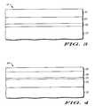
- FIG. 8illustrates a high resolution Transmission Electron Micrograph of a structure including an amorphous oxide layer
- FIG. 9illustrates an x-ray diffraction spectrum of a structure including an amorphous oxide layer
- FIGS. 10-13illustrate schematically, in cross-section, the formation of a device structure in accordance with another embodiment of the invention.
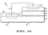
- FIG. 14illustrates schematically, in cross-section, the formation of a device structure in accordance with still another embodiment of the invention.
- FIG. 1illustrates schematically, in cross section, a portion of a semiconductor structure 20 in accordance with an embodiment of the invention.
- Semiconductor structure 20includes a monocrystalline substrate 22 , accommodating buffer layer 24 comprising a monocrystalline material, and a monocrystalline material layer 26 .
- the term “monocrystalline”shall have the meaning commonly used within the semiconductor industry.
- the termshall refer to materials that are a single crystal or that are substantially a single crystal and shall include those materials having a relatively small number of defects such as dislocations and the like as are commonly found in substrates of silicon or germanium or mixtures of silicon and germanium and epitaxial layers of such materials commonly used in the semiconductor industry.
- structure 20also includes an amorphous intermediate layer 28 positioned between substrate 22 and accommodating buffer layer 24 .
- Structure 20may also include a template layer 30 between the accommodating buffer layer and monocrystalline material layer 26 .
- the template layerhelps to initiate the growth of the monocrystalline material layer on the accommodating buffer layer.
- the amorphous intermediate layerhelps to relieve the strain in the accommodating buffer layer and, by doing so, aids in the growth of a high crystalline quality accommodating buffer layer.
- Substrate 22is a monocrystalline semiconductor or compound semiconductor wafer, preferably of large diameter.
- the wafercan be of, for example, a material from Group IV of the periodic table.
- Group IV semiconductor materialsinclude silicon, germanium, mixed silicon and germanium, mixed silicon and carbon, mixed silicon, germanium and carbon, and the like.
- substrate 22is a wafer containing silicon or germanium, and most preferably is a high quality monocrystalline silicon wafer as used in the semiconductor industry.
- Substrate 22may also include an epitaxial layer (not illustrated) to facilitate the fabrication of semiconductor devices as will be explained more fully below.
- Accommodating buffer layer 24is preferably a monocrystalline oxide or nitride material epitaxially grown on the underlying substrate.
- amorphous intermediate layer 28is grown on substrate 22 at the interface between substrate 22 and the growing accommodating buffer layer by the oxidation of substrate 22 during the growth of layer 24 .
- the amorphous intermediate layerserves to relieve strain that might otherwise occur in the monocrystalline accommodating buffer layer as a result of differences in the lattice constants of the substrate and the buffer layer.
- lattice constantrefers to the distance between atoms of a cell measured in the plane of the surface. If such strain is not relieved by the amorphous intermediate layer, the strain may cause defects in the crystalline structure of the accommodating buffer layer.
- monocrystalline material layer 26which may comprise a semiconductor material, a compound semiconductor material, a monocrystalline oxide layer, or another type of material such as a metal or a non-metal.
- Accommodating buffer layer 24is preferably a monocrystalline oxide or nitride material selected for its crystalline compatibility with the underlying substrate and with the overlying material layer.
- the materialcould be an oxide or nitride having a lattice structure closely matched to the substrate and to the subsequently applied monocrystalline material layer.
- Materials that are suitable for the accommodating buffer layerinclude metal oxides such as the alkaline earth metal/transition metal oxides such as alkaline earth metal titanates, alkaline earth metal zirconates, alkaline earth metal hafnates, alkaline earth metal tantalates, alkaline earth metal ruthenates, alkaline earth metal niobates, alkaline earth metal vanadates, alkaline earth metal tin-based perovskites, lanthanum aluminate, lanthanum scandium oxide, gadolinium oxide, other perovskite oxide materials, and other monocrystalline metal oxides.
- the alkaline earth metal/transition metal oxidessuch as alkaline earth metal titanates, alkaline earth metal zirconates, alkaline earth metal hafnates, alkaline earth metal tantalates, alkaline earth metal ruthenates, alkaline earth metal niobates, alkaline earth metal vanadates, alkaline earth metal tin-based perovskites,
- nitridessuch as gallium nitride, aluminum nitride, and boron nitride may also be used for the accommodating buffer layer.
- Most of these materialsare insulators, although strontium ruthenate, for example, is a conductor.
- these materialsare metal oxides or metal nitrides, and more particularly, these metal oxide or nitrides typically, although not necessarily, include at least two different metallic elements. In some specific applications, the metal oxides or nitrides may include three or more different metallic elements.
- Amorphous interface layer 28is preferably an oxide formed by the oxidation of the surface of substrate 22 , and more preferably is composed of a silicon oxide.
- the thickness of layer 28is sufficient to relieve strain attributed to mismatches between the lattice constants of substrate 22 and accommodating buffer layer 24 .
- layer 28has a thickness in the range of approximately 0.5-5 nanometers (nm). As will be explained more fully below, in certain applications the thickness of the amorphous layer should be minimized, especially during the initial stages of the growth of the monocrystalline buffer layer.
- the material for monocrystalline material layer 26can be selected, as necessary, for a particular structure or application.
- the monocrystalline material of layer 26may comprise a compound semiconductor which can be selected, as needed for a particular semiconductor structure, from any of the Group IIIA and VA elements (III-V semiconductor compounds), mixed III-V compounds, Group II (A or B) and VIA elements (II-VI semiconductor compounds), mixed II-VI compounds, Group IV and VI elements (IV-VI semiconductor compounds), mixed IV-VI compounds, Group IV element (Group IV semiconductors), and mixed Group IV compounds.
- Examplesinclude gallium arsenide (GaAs), gallium indium arsenide (GaInAs), gallium aluminum arsenide (GaAlAs), indium phosphide (InP), cadmium sulfide (CdS), cadmium mercury telluride (CdHgTe), zinc selenide (ZnSe), zinc sulfur selenide (ZnSSe), lead selenide (PbSe), lead telluride (PbTe), lead sulfide selenide (PbSSe), silicon (Si), germanium (Ge), silicon germanium (SiGe), silicon germanium carbide (SiGeC), and the like.
- monocrystalline material layer 26may also comprise other semiconductor materials, monocrystalline oxides, metals, or non-metal materials which are used in the formation of semiconductor structures, devices and/or integrated circuits.
- template layer 30has a thickness ranging from about 1 to about 10 monolayers.
- a monolayer of a perovskite oxide, such as SrTiO 3is defined as a layer of such an oxide having a thickness of its unit cell length along the growth direction.
- a monolayer of one of its components, such as a monolayer of Sris defined as the equivalent amount of atoms of this type, in this case the Sr atoms, contained in a monolayer of such an oxide.
- the templatemay also incorporate a wetting layer which helps to initiate high quality two dimensional crystalline growth.
- FIG. 2illustrates, in cross section, a portion of a semiconductor structure 40 in accordance with a further embodiment of the invention.
- Structure 40is similar to the previously described semiconductor structure 20 , except that an additional buffer layer 32 is positioned between accommodating buffer layer 24 and monocrystalline material layer 26 .
- the additional buffer layeris positioned between template layer 30 and the overlying layer of monocrystalline material.
- the additional buffer layerformed of a semiconductor or compound semiconductor material when the monocrystalline material layer 26 comprises a semiconductor or compound semiconductor material, serves to provide a lattice compensation when the lattice constant of the accommodating buffer layer cannot be adequately matched to the overlying monocrystalline semiconductor or compound semiconductor material layer.
- semiconductor structure 31includes, in accordance with a further embodiment of the invention, a monocrystalline semiconductor substrate 22 , amorphous intermediate layer 28 , accommodating buffer layer 24 , and overlying layer 33 .
- the overlying layermay or may not be monocrystalline.
- layer 33may be polycrystalline silicon used for the fabrication of a gate electrode.
- Accommodating buffer layer 24in such embodiment, could be used as a gate dielectric of the field effect transistor.
- layer 24is not an “accommodating buffer” as that term is used elsewhere in this disclosure, i.e., a monocrystalline layer providing an accommodation of underlying and overlying crystal lattice constants; but for sake of consistency, any monocrystalline layer grown overlying substrate 22 will be referred to by that term.
- FIG. 4schematically illustrates, in cross section, a portion of a semiconductor structure 34 in accordance with another exemplary embodiment of the invention.
- Structure 34is similar to structure 20 , except that structure 34 includes an amorphous layer 36 , rather than accommodating buffer layer 24 and amorphous interface layer 28 , and an additional monocrystalline layer 38 .
- amorphous layer 36may be formed by first forming an accommodating buffer layer and an amorphous interface layer in a similar manner to that described above. Monocrystalline layer 38 is then formed (by epitaxial growth) overlying the monocrystalline accommodating buffer layer. The accommodating buffer layer then optionally may be exposed to an anneal process to convert at least a portion of the monocrystalline accommodating buffer layer to an amorphous layer.
- Amorphous layer 36 formed in this mannercomprises materials from both the accommodating buffer and interface layers, which amorphous layers may or may not amalgamate. Thus, layer 36 may comprise one or two amorphous layers. Formation of amorphous layer 36 between substrate 22 and additional monocrystalline layer 26 (subsequent to layer 38 formation) relieves stresses between layers 22 and 38 and provides a true compliant substrate for subsequent processing—e.g., monocrystalline material layer 26 formation.
- Additional monocrystalline layer 38may include any of the materials described throughout this application in connection with either of monocrystalline material layer 26 or additional buffer layer 32 .
- layer 38may include monocrystalline Group IV or monocrystalline compound semiconductor materials.
- additional monocrystalline layer 38serves as an anneal cap during layer 36 formation and as a template for subsequent monocrystalline layer 26 formation. Accordingly, layer 38 is preferably thick enough to provide a suitable template for layer 26 growth (at least one monolayer) and thin enough to allow layer 38 to form as a substantially defect free monocrystalline material layer.
- additional monocrystalline layer 38comprises monocrystalline material (e.g., a material discussed above in connection with monocrystalline layer 26 ) that is thick enough to allow the formation of devices therein.
- monocrystalline materiale.g., a material discussed above in connection with monocrystalline layer 26
- a semiconductor structure in accordance with the present inventiondoes not include monocrystalline material layer 26 .
- the semiconductor structure in accordance with this embodimentincludes only one monocrystalline layer disposed above amorphous oxide layer 36 .
- monocrystalline substrate 22is a silicon substrate oriented in the (100) direction.
- the silicon substratecan be, for example, a silicon substrate as is commonly used in making complementary metal oxide semiconductor (CMOS) integrated circuits having a diameter of about 200-300 mm.
- accommodating buffer layer 24is a monocrystalline layer of Sr z Ba 1 ⁇ z TiO 3 where z ranges from 0 to 1 and the amorphous intermediate layer is a layer of silicon oxide (SiO x ) formed at the interface between the silicon substrate and the accommodating buffer layer. The value of z is selected to obtain one or more lattice constants closely matched to corresponding lattice constants of the underlying substrate and subsequently formed layer 26 .
- the accommodating buffer layercan have a thickness of about 2 to about 100 nanometers (nm) and preferably has a thickness of about 5 nm. In general, it is desired to have an accommodating buffer layer thick enough to isolate the monocrystalline material layer 26 from the substrate to obtain the desired electrical and optical properties. Layers thicker than 100 nm usually provide little additional benefit while increasing cost unnecessarily; however, thicker layers may be fabricated if needed.
- the amorphous intermediate layer of silicon oxidecan have a thickness of about 0.5-5 nm, and preferably a thickness of about 1 to 2 nm.
- monocrystalline material layer 26is a compound semiconductor layer of gallium arsenide (GaAs) or aluminum gallium arsenide (AlGaAs) having a thickness of about 1 nm to about 100 micrometers ( ⁇ m) and preferably having a thickness of about 0.5 ⁇ m to 10 ⁇ m. The thickness generally depends on the application for which the layer is being prepared. To facilitate the epitaxial growth of the gallium arsenide or aluminum gallium arsenide on the monocrystalline oxide, the oxide layer is capped with a template layer.
- GaAsgallium arsenide
- AlGaAsaluminum gallium arsenide
- the template layeris preferably 0.5-10 monolayers of Ti—As, Ti—O—As, Ti—O—Ga, Sr—O—As, Sr—Ga—O, or Sr—Al—O.
- 0.5-2 monolayers of Ti—As or Ti—O—Ashave been found effective to successfully grow GaAs layers.
- the template layercan also include a wetting layer on its upper surface. As explained more fully below, the wetting layer is formed of a material that changes the surface energy of the accommodating buffer layer to aid in the monocrystalline growth of the overlying layer.
- Suitable materials for the wetting layerinclude, for example, metals, intermetallics, and metal oxides having a cubic crystalline structure. Examples of such materials include NiAl, FeAl, CoAl, Ni, Co, Fe, Cu, Ag, Au, Ir, Rh, Pt, Pd, Rb, Cs, CoO, FeO, Cu 2 O, Rb 2 O 3 , Cs 2 O 3 , and NiO.
- the thickness of the wetting layeris preferably 0.5-5.0 monolayers.
- monocrystalline substrate 22is a silicon substrate as described above.
- the accommodating buffer layeris a monocrystalline oxide of strontium or barium zirconate or hafnate in a cubic or orthorhombic phase with an amorphous intermediate layer of silicon oxide formed at the interface between the silicon substrate and the accommodating buffer layer.
- the accommodating buffer layercan have a thickness of about 2-100 nm and preferably has a thickness of at least 4 nm to ensure adequate crystalline and surface quality and is formed of a monocrystalline SrZrO 3 , BaZrO 3 , SrHfO 3 , BaSnO 3 or BaHfO 3 .
- the accommodating buffer layercan be a monocrystalline oxide layer of BaZrO 3 grown at a temperature of about 700 degrees C.
- the lattice structure of the resulting crystalline oxideexhibits a 45 degree rotation with respect to the substrate silicon lattice structure.
- an accommodating buffer layer formed of these zirconate or hafnate materialsis suitable for the growth of a monocrystalline material layer which comprises compound semiconductor materials in the indium phosphide (InP) system.
- the compound semiconductor materialcan be, for example, indium phosphide (InP), indium gallium arsenide (InGaAs), aluminum indium arsenide, (AlInAs), or aluminum gallium indium arsenide phosphide (AlGaInAsP), having a thickness of about 1.0 nm to 10 ⁇ m.
- a suitable template for this structureis about 0.5-10 monolayers of one of a material M—N or a material M—O—N, wherein M is selected from at least one of Zr, Hf, Ti, Sr, and Ba and N is selected from at least one of As, P, Ga, Al, and In.
- the templateis about 0.5-2 monolayers of one of these materials.
- the surfaceis terminated with 0.5-2 monolayers of zirconium followed by deposition of 0.5-2 monolayers of arsenic to form a Zr—As template.
- the template layermay be completed with an appropriate wetting layer to facilitate the two dimensional monocrystalline growth of a subsequent layer.
- a monocrystalline layer of the compound semiconductor material from the indium phosphide systemis then grown on the template layer.
- the resulting lattice structure of the compound semiconductor materialexhibits a 45 degree rotation with respect to the accommodating buffer layer lattice structure and a lattice mismatch to (100) InP of less than 2.5%, and preferably less than about 1.0%.
- a structureis provided that is suitable for the growth of an epitaxial film of a monocrystalline material comprising a II-VI material overlying a silicon substrate.
- the substrateis preferably a silicon wafer as described above.
- a suitable accommodating buffer layer materialis Sr x Ba 1 ⁇ x TiO 3 , where x ranges from 0 to 1, having a thickness of about 2-100 nm and preferably a thickness of about 3-10 nm.
- the monocrystalline II-VI compound semiconductor material grown epitaxially overlying the accommodating buffer layercan be, for example, zinc selenide (ZnSe) or zinc sulfur selenide (ZnSSe).
- a suitable template for this material systemincludes 0.5-10 monolayers of zinc-oxygen (Zn—O) followed by 0.5-2 monolayers of an excess of zinc followed by the selenidation of zinc on the surface.
- a templatecan be, for example, 0.5-10 monolayers of strontium-sulfur (Sr—S) followed by the ZnSSe.
- the templatecan also include an appropriate wetting layer.
- This embodiment of the inventionis an example of structure 40 illustrated in FIG. 2 .
- Substrate 22 , accommodating buffer layer 24 , and monocrystalline material layer 26can be similar to those described in example 1.
- an additional buffer layer 32serves to alleviate any strains that might result from a mismatch between the crystal lattice of the accommodating buffer layer and the lattice of the overlying monocrystalline material.
- Buffer layer 32can be a layer of germanium or a strain compensated superlattice of GaAs, aluminum gallium arsenide (AlGaAs), indium gallium phosphide (InGaP), aluminum gallium phosphide (AlGaP), indium gallium arsenide (InGaAs), aluminum indium phosphide (AlInP), gallium arsenide phosphide (GaAsP), or indium gallium phosphide (InGaP).
- buffer layer 32includes a GaAs x P 1 ⁇ x superlattice, wherein the value of x ranges from 0 to 1.
- buffer layer 32includes an In y Ga 1 ⁇ y P superlattice, wherein the value of y ranges from 0 to 1.
- the lattice constantis varied from bottom to top across the superlattice to create a match between lattice constants of the underlying oxide and the overlying monocrystalline material which, in this example, is a compound semiconductor material.
- the compositions of other compound semiconductor materials, such as those listed above,may also be similarly varied to manipulate the lattice constant of layer 32 in a like manner.
- the superlatticecan have a thickness of about 50-500 nm and preferably has a thickness of about 100-200 nm.
- the superlattice periodcan have a thickness of about 2-15 nm, preferably, 2-10 nm.
- the template for this structurecan be the same of that described in Example 1.
- buffer layer 32can be a layer of monocrystalline germanium having a thickness of 1-50 nm and preferably having a thickness of about 2-20 nm.
- a template layer of either germanium-strontium (Ge—Sr) or germanium-titanium (Ge—Ti) having a thickness of about 0.5-2 monolayerscan be used as a nucleating site for the subsequent growth of the monocrystalline germanium layer.
- the formation of the accommodating buffer layeris capped with either 0.5-1 monolayer of strontium or 0.5-1 monolayer of titanium to act as a nucleating site for the subsequent deposition of the monocrystalline germanium.
- the layer of strontium or titaniumprovides a nucleating site to which the first monolayer of germanium can bond.
- the same wetting agents described above in Example 1can be used to initiate high quality two dimensional growth of the germanium layer.
- Substrate material 22 , accommodating buffer layer 24 , monocrystalline material layer 26 and template layer 30can be the same as those described above in Example 2.
- additional buffer layer 32is inserted between the accommodating buffer layer and the overlying monocrystalline material layer.
- the buffer layera further monocrystalline material which, in this example, comprises a semiconductor material, can be, for example, a graded layer of indium gallium arsenide (InGaAs) or indium aluminum arsenide (InAlAs).
- additional buffer layer 32includes InGaAs in which the indium in the composition varies from 0 to about 50%.
- the additional buffer layer 32preferably has a thickness of about 10-30 nm. Varying the composition of the buffer layer from GaAs to InGaAs serves to provide a lattice match between the underlying monocrystalline oxide material and the overlying layer of monocrystalline material which in this example is a compound semiconductor material. Such a buffer layer is especially advantageous if there is a lattice mismatch between accommodating buffer layer 24 and monocrystalline material layer 26 .
- Substrate material 22is, for example, a monocrystalline silicon wafer as commonly used in the semiconductor industry for the fabrication of semiconductor devices and integrated circuits. Depending on the device or integrated circuit to be fabricated, the wafer may be a bulk wafer or it may be a bulk wafer having an epitaxial silicon layer formed on the top surface thereof. Impurity doped regions may be formed in the substrate as, for example, source and drain regions of a field effect transistor.
- Amorphous intermediate layer 28is a silicon oxide formed by the oxidation of the surface of the silicon substrate.
- Accommodating buffer layer 24is a monocrystalline layer of strontium titanate having an initial thickness of 1-10 monolayers, and preferably an initial thickness of 3-6 monolayers.
- Layer 33 formed overlying the accommodating buffer layeris a layer of polycrystalline silicon from which a gate electrode of the field effect transistor will be formed.
- the layer of strontium titanateserves as a gate dielectric of the transistor.
- layer 33can be a layer of monocrystalline strontium zirconate to form a so called “medium k” dielectric of the transistor.
- a gate electrodewould then be formed overlying the strontium zirconate dielectric layer. In the fabrication of semiconductor structure 31 , it may be advantageous to minimize the thickness of amorphous intermediate layer 28 .
- the amorphous intermediate layeris one component of the gate dielectric of the field effect transistor, and it is usually desirable to minimize that dielectric thickness. Additionally, the silicon oxide that forms the amorphous intermediate layer is also a relatively “low k” dielectric and is thus to be minimized.
- Substrate material 22 , template layer 30 , and monocrystalline material layer 26may be the same as those described above in connection with example 1.
- Amorphous layer 36is an amorphous oxide layer which is suitably formed of a combination of amorphous intermediate layer materials (e.g., layer 28 materials as described above) and accommodating buffer layer materials (e.g., layer 24 materials as described above).
- amorphous layer 36may include a combination of SiO x and Sr z Ba 1 ⁇ z TiO 3 (where z ranges from 0 to 1) which combine or mix, at least partially, during an anneal process to form amorphous oxide layer 36 .
- amorphous layer 36may vary from application to application and may depend on such factors as desired insulating properties of layer 36 , type of monocrystalline material comprising layer 26 , and the like. In accordance with one exemplary aspect of the present embodiment, layer 36 thickness is about 1 nm to about 100 nm, preferably about 1-10 nm, and more preferably about 3-5 nm.
- Layer 38comprises a monocrystalline material that can be grown epitaxially over a monocrystalline oxide material such as the material used to form accommodating buffer layer 24 .
- layer 38includes the same materials as those comprising layer 26 .
- layer 38also includes GaAs.
- layer 38may include materials different from those used to form layer 26 .
- layer 38if formed to a thickness of about 1 nm to about 500 nm.
- substrate 22is a monocrystalline substrate such as, for example, a monocrystalline silicon or gallium arsenide substrate.
- the crystalline structure of the monocrystalline substrateis characterized by a lattice constant and by a lattice orientation.
- accommodating buffer layer 24is also a monocrystalline material and the lattice of that monocrystalline material is characterized by a lattice constant and a crystal orientation.
- the lattice constants of the accommodating buffer layer and the monocrystalline substratemust be substantially equal or, alternatively, must be such that upon rotation of one crystal orientation with respect to the other crystal orientation, a substantial match in lattice constants is achieved.
- the terms “substantially equal” and “substantial match”mean that there is sufficient similarity between the lattice constants to permit the growth of a high quality crystalline layer on the underlying layer.
- FIG. 5illustrates graphically the relationship of the achievable thickness of a grown crystal layer of high crystalline quality as a function of the mismatch between the lattice constants of the host crystal and the grown crystal.
- Curve 42illustrates the boundary of high crystalline quality material. The area to the right of curve 42 represents layers that have a large number of defects. With no lattice mismatch, it is theoretically possible to grow an infinitely thick, high quality epitaxial layer on the host crystal. As the mismatch in lattice constants increases, the thickness of achievable, high quality crystalline layer decreases rapidly. As a reference point, for example, if the lattice constants between the host crystal and the grown layer are mismatched by more than about 2%, monocrystalline epitaxial layers in excess of about 20 nm cannot be achieved.
- substrate 22is a (100) oriented monocrystalline silicon wafer and accommodating buffer layer 24 is a layer of strontium barium titanate.
- Substantial matching of lattice constants between these two materialsis achieved by suitably choosing the ratio of strontium to barium and by rotating the crystal orientation of the titanate material by 45° with respect to the crystal orientation of the silicon substrate wafer.
- the inclusion in the structure of amorphous interface layer 28a silicon oxide layer in this example, if it is of sufficient thickness, serves to reduce strain in the monocrystalline titanate layer that might result from any mismatch in the lattice constants of the host silicon wafer and the grown titanate layer.
- a high quality, thick, monocrystalline titanate layeris achievable.
- layer 26is a layer of epitaxially grown monocrystalline material and that crystalline material is also characterized by a crystal lattice constant and a crystal orientation.
- the lattice constant of layer 26differs from the lattice constant of substrate 22 .
- the accommodating buffer layermust be of high crystalline quality.
- substantial matching between the crystal lattice constant of the host crystal, in this case, the monocrystalline accommodating buffer layer, and the grown crystalis desired.
- this substantial matching of lattice constantsis achieved as a result of rotation of the crystal orientation of the grown crystal with respect to the orientation of the host crystal.
- the grown crystalis gallium arsenide, aluminum gallium arsenide, zinc selenide, or zinc sulfur selenide and the accommodating buffer layer is monocrystalline Sr x Ba 1 ⁇ x TiO 3
- substantial matching of crystal lattice constants of the two materialsis achieved by a suitable choice for x and by rotating the crystal orientation of the grown layer by 45° with respect to the orientation of the host monocrystalline oxide.
- the host materialis a strontium or barium zirconate or a strontium or barium hafnate or barium tin oxide and the compound semiconductor layer is indium phosphide or gallium indium arsenide or aluminum indium arsenide
- substantial matching of crystal lattice constantscan be achieved proper choice of the host oxide material and by rotating the orientation of the grown crystal layer by 45° with respect to the host oxide crystal.
- a crystalline semiconductor buffer layer between the host oxide and the grown monocrystalline material layercan be used to reduce strain in the grown monocrystalline material layer that might result from small differences in lattice constants. Better crystalline quality in the grown monocrystalline material layer can thereby be achieved.
- the following exampleillustrates a process, in accordance with one embodiment of the invention, for fabricating a semiconductor structure such as the structures depicted in FIGS. 1-4 .
- the processstarts by providing a monocrystalline semiconductor substrate comprising silicon or germanium.
- the semiconductor substrateis a silicon wafer having a (100) orientation.
- the substrateis oriented on axis or, if desired, up to 8° off axis towards any desired crystallographic direction.
- At least a portion of the semiconductor substratehas a bare surface, although other portions of the substrate may encompass other structures.
- the term “bare” in this contextmeans that the surface in that portion of the substrate has been cleaned to remove any oxides, contaminants, or other foreign material.
- bare siliconis highly reactive and readily forms a native oxide.
- the term “bare”is intended to encompass such a native oxide.
- a thin silicon oxideis then intentionally grown on the semiconductor substrate.
- the thin silicon oxideis grown immediately prior to the formation of the monocrystalline accommodating buffer layer, and can be grown by thermal or chemical oxidation of the silicon surface.
- the thin silicon oxideis grown by exposing the substrate surface to an ultraviolet (UV) lamp in the presence of ozone for a time period of up to about 20 minutes.
- UVultraviolet
- the semiconductor substratecan be exposed to an rf or an ECR oxygen plasma. During such treatment the temperature of the substrate is maintained at a temperature of between 100° C. and 600° C. with an oxygen partial pressure of 10 ⁇ 5 to 10 ⁇ 8 millibar (mbar).
- the thin silicon oxidecan be grown by exposing the substrate to an ozone ambient at an elevated temperature in the same processing apparatus, such as a molecular beam epitaxial (MBE) reactor, used for the subsequent deposition of the accommodating buffer layer.
- MBEmolecular beam epitaxial
- the native and/or grown oxide layermust first be removed to expose the crystalline structure of the underlying substrate.
- the following processis preferably carried out by molecular beam epitaxy, although other epitaxial processes may also be used in accordance with the present invention.
- the native oxidecan be removed by first depositing a thin layer (preferably 1-3 monolayers) of strontium, barium, a combination of strontium and barium, or other alkaline earth metals or combinations of alkaline earth metals onto the substrate in an MBE apparatus. In the case where strontium is used, the substrate is then heated to a temperature above 700° C. to cause the strontium to react with the native silicon oxide layer.
- the strontiumserves to reduce the silicon oxide to leave a silicon oxide-free surface.
- the resultant surfacemay exhibit an ordered 2 ⁇ 1 structure. If an ordered (2 ⁇ 1) reconstruction has not been achieved at this stage of the process, the structure may be exposed to additional strontium until an ordered (2 ⁇ 1) reconstruction is obtained.
- the ordered 2 ⁇ 1 reconstructionforms a template for the ordered growth of an overlying layer of a monocrystalline oxide.
- the templateprovides the necessary chemical and physical properties to nucleate the crystalline growth of an overlying layer.
- the native silicon oxidecan be converted and the substrate surface can be prepared for the growth of a monocrystalline oxide layer by depositing an alkaline earth metal oxide, such as strontium oxide, strontium barium oxide, or barium oxide, onto the substrate surface by MBE at a low temperature and by subsequently heating the structure to a temperature of above 700° C. At this temperature a solid state reaction takes place between the strontium oxide and the native silicon oxide causing the reduction of the native silicon oxide and leaving an ordered 2 ⁇ 1 reconstruction on the substrate surface. If an ordered (2 ⁇ 1) reconstruction has not been achieved at this stage of the process, the structure may be exposed to additional strontium until an ordered (2 ⁇ 1) reconstruction is obtained.
- an alkaline earth metal oxidesuch as strontium oxide, strontium barium oxide, or barium oxide
- a monocrystalline oxide layer on the substratecan begin. This growth is accomplished in the same apparatus, preferably an MBE reactor, as is the surface preparation. During the growth of the monocrystalline oxide layer overlying the monocrystalline silicon substrate, reactants, including oxygen, are introduced to the MBE reactor. Under proper conditions the reactants react at the silicon surface to grow the desired monocrystalline oxide. Because of the presence of the oxygen, however, a competing reaction, that of oxidizing the silicon substrate, can also occur.
- the growth processshould be controlled to suppress the competing reaction of the oxygen with the silicon substrate, a reaction that causes oxidation of the silicon substrate and disrupts the ordered two dimensional growth of the monocrystalline oxide layer.
- a layer of amorphous oxide underlying the monocrystalline oxide layermay be desirable for reducing strain in the monocrystalline oxide layer, that amorphous layer must be grown after the monocrystalline growth has been sufficiently initiated.
- the ordered two dimensional growth of a high quality monocrystalline oxide layersuch as a layer of monocrystalline strontium titanate, overlying an oxidizable monocrystalline substrate, such as a silicon substrate, can be accomplished by the following process.
- the processsuppresses the oxidation of the substrate material (i.e., in the case of a silicon substrate, oxidation of the silicon substrate to grow an amorphous silicon oxide layer) while allowing the oxidation of strontium and titanium to grow monocrystalline strontium titanate.
- the substrateis cooled to a temperature between room temperature and about 400° C., and preferably to a temperature of about 300° C.
- the initial growth of the strontium titanate monocrystalline layerwill take place at this lowered temperature.
- the oxidation of strontium and titanium to form strontium titanateis favored over the oxidation of the silicon substrate.
- the higher the temperaturethe greater the oxidation rate of both the silicon oxide and the strontium titanate components.
- the higher the partial pressure of oxygen in the reactorthe greater the oxidation rate of both the silicon substrate and the strontium titanate components strontium and titanium.
- the temperature selectedshould be as high as possible without incurring deleterious amounts of silicon oxidation.
- oxygenis introduced into the reactor to establish a partial pressure of oxygen in the reactor of between about 2 ⁇ 10 ⁇ 8 mbar and about 3 ⁇ 10 ⁇ 7 mbar.
- the exact pressure selectedwill depend on some physical parameters of the reactor such as the size of the reactor chamber and the reactor pumping capacity.
- the partial pressure selectedshould be high enough to grow stoichiometric strontium titanate but not too high to cause significant oxidation of Si.
- the strontium and titanium shutters of the MBE reactorare then opened to introduce strontium and titanium to the reaction.
- the ratio of strontium and titaniumis adjusted to approximately 1:1 to grow stoichiometric strontium titanate.
- the shuttersare closed and the oxygen flow is terminated to reduce the oxygen partial pressure in the reactor chamber to less than about 5 ⁇ 10 ⁇ 9 mbar.
- the 1-3 monolayers of strontium titanateform on the silicon surface as an ordered two dimensional monocrystalline layer without significant oxidation of the silicon surface. Grown at 300° C., the order parameter of the strontium titanate layer is not high. That is, the film, although monocrystalline, is not of high crystalline quality.
- the temperature of the substrateis then raised to about 500-750° C. and preferably to about 650° C. to anneal the monocrystalline strontium titanate layer and to thereby improve the crystalline quality of the layer.
- the titanate layerbecomes much more ordered.
- the ordering of the layercan be monitored in real time, preferably by observing RHEED patterns from the surface.
- the substrateis maintained at the elevated temperature until the intensity of the RHEED pattern begins to flatten out. This indicates that the ordering of the monocrystalline strontium titanate layer has saturated.
- the anneal at the elevated temperaturepreferably less than 15 minutes, is terminated after the saturation is observed. Following the annealing process, the temperature of the substrate is again reduced and the growth process is initiated again.
- the growth temperaturecan be raised, for example to 400° C.
- oxygenis again introduced into the reactor chamber and the partial pressure of oxygen is set to a value equal to or greater than the partial pressure maintained during the previous deposition.
- the titanium and strontium shuttersare opened and an additional 1-3 monolayers of monocrystalline strontium titanate is grown overlying the silicon substrate.
- the additional strontium titanatecan then be annealed, as above, to improve the crystallinity of the layer.
- the steps of growth followed by annealcan be repeated to increase the thickness of the monocrystalline oxide layer.
- a monocrystalline strontium titanate layer having a thickness greater than about 5 monolayershas been grown on the silicon substrate, the silicon substrate will be sufficiently isolated from the reactants and additional monocrystalline strontium titanate (if additional strontium titanate is necessary for the device structure being fabricated) can be grown at a higher temperature.
- additional strontium titanatecan be grown at a temperature between about 550° C. and about 950° C. and preferably at a temperature greater than about 650° C.
- the partial pressure of oxygencan be increased above the initial minimum value to cause the growth of an amorphous silicon oxide layer at the interface between the monocrystalline silicon substrate and the monocrystalline strontium titanate layer.
- This silicon oxidation stepmay be applied either during or after the growth of the strontium titanate layer.
- the growth of the silicon oxide layerresults from the diffusion of oxygen through the strontium titanate layer to the interface where the oxygen reacts with silicon at the surface of the underlying substrate. Strain that otherwise might exist in the strontium titanate layer because of the small mismatch in lattice constant between the silicon substrate and the growing crystal is relieved in the amorphous silicon oxide intermediate layer.
- a processhas been disclosed for growing a high quality monocrystalline strontium titanate layer on a silicon substrate.
- Other monocrystalline oxides, and specifically metal oxidescan be grown on monocrystalline substrates in similar manner by oxidizing the metal without oxidizing the underlying substrate.
- Thisincludes a series oxides such as SrZrO 3 , BaTiO 3 , Pb(Zr, Ti)O 3 , (Pb, La)(Zr, Ti)O 3 , LaAlO 3 , SrRuO 3 , YBCO, CeO 2 , ZrO 2 , and MgO etc.
- the principles of initiating growth at a low temperature to prevent the oxidization of the substrate and then anneal without the presence of the oxidant to improve the crystallinity at a small film thicknesscan be applied to any other oxides on any oxidizable substrates.
- the oxidantsare not limited to oxygen but can be any other reactants that oxidize the substrate, such as O 3 , H 2 O, N 2 O, N 2 , F 2 , Cl 2 , etc.
- the monocrystalline oxide grown in this manner overlying a monocrystalline substratecan be used as a starting material for many device structures.
- a monocrystalline oxide such as strontium titanatemay be used by itself as a high dielectric constant (“high k”) insulator of a field effect transistor.
- high khigh dielectric constant
- Other field effect devicesmay be formed in which the strontium titanate layer is used as an accommodating buffer layer for the growth of a medium k dielectric such as monocrystalline strontium zirconate.
- Monocrystalline strontium zirconateis difficult to grow on monocrystalline silicon, but can be grown on strontium titanate by a MBE process or by a sol-gel process.
- the monocrystalline strontium titanate layercan also be used as an accommodating buffer layer for forming other monocrystalline insulator layers such as PZT, PLZT, conducting layers such as SrRuO 3 , (La, Sr)CoO 3 , superconducting layers such as YBCO, BSCCO, binary oxides such as MgO, ZrO 2 , and even thick layers of strontium titanate. All of these can be formed on the monocrystalline strontium titanate by MBE, CBE, CVD, PVD, PLD, sol-gel process or by one of the other epitaxial growth processes described elsewhere in this disclosure. Other processes in which a monocrystalline accommodating buffer layer is formed on a monocrystalline substrate and a monocrystalline layer is formed on that accommodating buffer layer are described below in greater detail.
- the monocrystalline strontium titanatemay be capped by a template layer that is conducive to the subsequent growth of an epitaxial layer of a desired monocrystalline material.
- the MBE growth of the strontium titanate monocrystalline layercan be capped by terminating the growth with 0.5-2 monolayers of titanium, 0.5-2 monolayers of titanium-oxygen or with 0.5-2 monolayers of strontium-oxygen.
- arsenicis deposited to form a Ti—As bond, a Ti—O—As bond or a Sr—O—As bond.
- galliumis subsequently introduced to the reaction with the arsenic to form gallium arsenide.
- galliumcan be deposited on the capping layer to form a Sr—O—Ga bond, a Ti—Ga bond, or a Ti—O—Ga bond, and arsenic is subsequently introduced with the gallium to form the GaAs.
- the template layerbefore growth of the GaAs layer, is enhanced by adding a wetting layer to the top thereof. Without the wetting layer, three dimensional growth of the compound semiconductor layer often occurs at the initial nucleation stage. The occurrence of three dimensional growth is due to low surface and interface energies associated with the oxide (in this example strontium titanate) surface. Oxides are typically chemically and energetically more stable than metals and most electronic materials such as GaAs. The three dimensional growth results in the spotty localized growth of discrete GaAs patches. Upon further growth the patches may grow together, but not as a monocrystalline layer.
- a wetting layeris epitaxially grown on the upper surface of the accommodating buffer layer to raise the surface energy at the surface of the oxide layer.
- Useful wetting agentsinclude materials having a cubic crystalline structure selected from the group of metals, intermetallics, and metal oxides. Representative materials meeting these criteria include NiAl, FeAl, CoAl, Ni, Co, Fe, Cu, Ag, Au, Ir, Rh, Pt, Pd, Rb, Cs, CoO, FeO, Cu 2 O, Rb 2 O 3 , Cs 2 O 3 , and NiO.
- the selected wetting agentis deposited to a thickness of 0.5-5.0 monolayers on and as part of the template layer in the same process apparatus used for the deposition of the accommodating buffer layer.
- the accommodating buffer layeris strontium titanate, barium titanate, or barium stontium titanate and the desired monocrystalline compound semiconductor layer is GaAs or AlGaAs
- 0.5-5.0 monolayers of NiAlform a suitable wetting layer.
- the deposition of the NiAlis initiated with the deposition of Ni.
- FIG. 6is a high resolution Transmission Electron Micrograph (TEM) of semiconductor material manufactured in accordance with one embodiment of the present invention.
- Single crystal SrTiO 3 accommodating buffer layer 24was grown epitaxially on silicon substrate 22 .
- amorphous interfacial layer 28was formed which relieves strain due to lattice mismatch.
- GaAs compound semiconductor layer 26was then grown epitaxially using template layer 30 .
- FIG. 7illustrates an x-ray diffraction spectrum taken on a structure including GaAs monocrystalline layer 26 grown on silicon substrate 22 using accommodating buffer layer 24 .
- the peaks in the spectrumindicate that both accommodating buffer layer 24 and GaAs compound semiconductor layer 26 are single crystal and (100) orientated.
- the structure illustrated in FIG. 2can be formed by the process discussed above with the addition of an additional buffer layer deposition step.
- the additional buffer layer 32is formed overlying the template layer before the deposition of the monocrystalline material layer.
- the buffer layeris a monocrystalline material comprising a compound semiconductor superlattice, such a superlattice can be deposited, for example by MBE, on the template, including a wetting layer, as described above.
- the buffer layeris a monocrystalline material layer comprising a layer of germanium
- the process aboveis modified to cap the strontium titanate monocrystalline layer with a final layer of either strontium or titanium and then depositing a wetting layer formed of one of the wetting agents described above.
- the germanium buffer layerthen can be deposited directly on this template/wetting layer.
- Structure 34may be formed by growing an accommodating buffer layer 24 , forming an amorphous oxide layer 28 over substrate 22 , and growing semiconductor layer 38 over the accommodating buffer layer, as described above.
- the accommodating buffer layer and the amorphous oxide layerare then exposed to an anneal process sufficient to change the crystalline structure of the accommodating buffer layer from monocrystalline to amorphous, thereby forming an amorphous layer such that the combination of the amorphous oxide layer and the now amorphous accommodating buffer layer form a single amorphous oxide layer 36 .
- Layer 26is then subsequently grown over layer 38 .
- the anneal processmay be carried out subsequent to growth of layer 26 .
- layer 36is formed by exposing substrate 22 , the accommodating buffer layer, the amorphous oxide layer, and monocrystalline layer 38 to a rapid thermal anneal process with a peak temperature of about 700° C. to about 1000° C. and a process time of about 5 seconds to about 20 minutes.
- a rapid thermal anneal processwith a peak temperature of about 700° C. to about 1000° C. and a process time of about 5 seconds to about 20 minutes.
- suitable anneal processesmay be employed to convert the accommodating buffer layer to an amorphous layer in accordance with the present invention.
- laser annealing, electron beam annealing, or “conventional” thermal annealing processesmay be used to form layer 36 .
- an overpressure of one or more constituents of layer 38may be required to prevent degradation of that layer during the anneal process.
- the anneal environmentpreferably includes an overpressure of arsenic to mitigate degradation of layer 38 .
- layer 38 of structure 34may include any materials suitable for either of layers 32 or 26 . Accordingly, any deposition or growth methods described in connection with either layer 32 or 26 , may be employed to deposit layer 38 .
- FIG. 8is a high resolution TEM of semiconductor material manufactured in accordance with the embodiment of the invention illustrated in FIG. 4 .
- a single crystal SrTiO 3 accommodating buffer layerwas grown epitaxially on silicon substrate 22 .
- an amorphous interfacial layerwas formed as described above.
- additional monocrystalline layer 38comprising a compound semiconductor layer of GaAs was formed above the accommodating buffer layer and the accommodating buffer layer was exposed to an anneal process to form amorphous oxide layer 36 .
- FIG. 9illustrates an x-ray diffraction spectrum taken on a structure including additional monocrystalline layer 38 comprising a GaAs compound semiconductor layer and amorphous oxide layer 36 formed on silicon substrate 22 .
- the peaks in the spectrumindicate that GaAs compound semiconductor layer 38 is single crystal and (100) orientated and the lack of peaks around 40 to 50 degrees indicates that layer 36 is amorphous.
- the process described aboveillustrates a process for forming a semiconductor structure including a silicon substrate, an overlying oxide layer, and a monocrystalline material layer comprising a gallium arsenide compound semiconductor layer by the process of molecular beam epitaxy.
- the processcan also be carried out by the process of chemical vapor deposition (CVD), metal organic chemical vapor deposition (MOCVD), migration enhanced epitaxy (MEE), atomic layer epitaxy (ALE), physical vapor deposition (PVD), chemical solution deposition (CSD), pulsed laser deposition (PLD), or the like.
- CVDchemical vapor deposition
- MOCVDmetal organic chemical vapor deposition
- MEEmigration enhanced epitaxy
- ALEatomic layer epitaxy
- PVDphysical vapor deposition
- CSSDchemical solution deposition
- PLDpulsed laser deposition
- monocrystalline accommodating buffer layerssuch as alkaline earth metal titanates, zirconates, hafnates, tantalates, vanadates, ruthenates, and niobates, alkaline earth metal tin-based perovskites, other perovskites, lanthanum aluminate, lanthanum scandium oxide, gadolinium oxide, and other metal oxides can also be grown.
- other monocrystalline material layerscomprising other III-V, II-VI, and IV-VI monocrystalline compound semiconductors, semiconductors, metals and non-metals can be deposited overlying the monocrystalline oxide accommodating buffer layer.
- each of the variations of monocrystalline material layer and monocrystalline oxide accommodating buffer layeruses an appropriate template for initiating the growth of the monocrystalline material layer.
- the accommodating buffer layeris an alkaline earth metal zirconate
- the oxidecan be capped by a thin layer of zirconium.
- the deposition of zirconiumcan be followed by the deposition of arsenic or phosphorus to react with the zirconium as a precursor to depositing indium gallium arsenide, indium aluminum arsenide, or indium phosphide respectively.
- the monocrystalline oxide accommodating buffer layeris an alkaline earth metal hafnate, the oxide layer can be capped by a thin layer of hafnium.
- hafniumis followed by the deposition of arsenic or phosphorous to react with the hafnium as a precursor to the growth of an indium gallium arsenide, indium aluminum arsenide, or indium phosphide layer, respectively.
- strontium titanatecan be capped with a layer of strontium or strontium and oxygen and barium titanate can be capped with a layer of barium or barium and oxygen.
- Each of these depositionscan be followed by the deposition of arsenic or phosphorus to react with the capping material to form a template for the deposition of a monocrystalline material layer comprising compound semiconductors such as indium gallium arsenide, indium aluminum arsenide, or indium phosphide.
- a monocrystalline material layercomprising compound semiconductors such as indium gallium arsenide, indium aluminum arsenide, or indium phosphide.
- high quality two dimensional growth of the monocrystalline material layers overlying the monocrystalline oxide accommodating buffer layercan be promoted by incorporating an appropriate wetting layer into the template layer.
- the wetting layerdeposited to a thickness of 0.5-5.0 monolayers in the same apparatus used for the deposition or growth of the monocrystalline material layer, serves to alter the surface energy of the monocrystalline oxide.
- the accommodating buffer layeris SrTiO 3 and the monocrystalline material layer is GaAs
- the monocrystalline material layeris GaAs
- the following relationshipmust be satisfied: ⁇ STO >( ⁇ INT + ⁇ GaAs ) where the surface energy of the monocrystalline SrTiO 3 accommodating buffer oxide layer must be greater than the energy of the interface between the accommodating buffer layer and the GaAs layer added to the surface energy of the GaAs layer.
- a wetting layerformed, for example from epitaxially grown NiAl, increases the surface energy of the monocrystalline oxide layer and also shifts the crystalline structure of the template to a diamond-like structure that is in compliance with the GaAs layer.
- a wetting agent containing template layeraids in the formation of a compliant substrate for the monolithic integration of various material layers including those comprised of Group III-V compounds to form high quality semiconductor structures, devices and integrated circuits.
- a wetting agent containing templatemay be used for the monolithic integration of a monocrystalline material layer such as a layer comprising germanium to form high efficiency photocells.
- FIGS. 10-13the formation of a device structure in accordance with still another embodiment of the invention is illustrated in cross-section.
- This embodimentutilizes the formation of a compliant substrate which relies on the epitaxial growth of single crystal oxides on silicon followed by the epitaxial growth of single crystal silicon onto the oxide.
- An accommodating buffer layer 74such as a monocrystalline oxide layer is first grown on a substrate layer 72 , such as silicon, with an amorphous interface layer 78 as illustrated in FIG. 10 .
- Monocrystalline oxide layer 74may be comprised of any of those materials previously discussed with reference to layer 24 in FIGS. 1-4
- amorphous interface layer 78is preferably comprised of any of those materials previously described with reference to the layer 28 illustrated in FIGS. 1-4 .
- Substrate 72although preferably silicon, may also comprise any of those materials previously described with reference to substrate 22 in FIGS. 1-4 .
- a silicon layer 81is deposited over monocrystalline oxide layer 74 via MBE, CVD, MOCVD, MEE, ALE, PVD, CSD, PLD, and the like as illustrated in FIG. 11 with a thickness of a few tens of nanometers but preferably with a thickness of about 5 nm.
- Monocrystalline oxide layer 74preferably has a thickness of about 2 to 10 nm.
- Rapid thermal annealingis then conducted in the presence of a carbon source such as acetylene or methane, for example at a temperature within a range of about 800° C. to 1000° C., to form capping layer 82 and amorphous silicate layer 86 .
- a carbon sourcesuch as acetylene or methane
- Other suitable carbon sourcesmay also be used.
- the purpose of the rapid thermal annealing step in the presence of a carbon sourceis to amorphize monocrystalline oxide layer 74 and to convert that monocrystalline layer into an amorphous silicate layer 86 .
- the rapid thermal annealingalso serves to carbonize the topmost portion of silicon layer 81 to form capping layer 82 .
- the capping layeris a silicon carbide (SiC) layer as illustrated in FIG. 12 .
- the formation of amorphous layer 86is similar to the formation of layer 36 illustrated in FIG. 4 and may comprise any of those materials described with reference to layer 36 in FIG. 4 .
- a compound semiconductor layer 96such as gallium nitride (GaN) is grown over the SiC surface by MBE, CVD, MOCVD, MEE, ALE, PVD, CSD, PLD, or the like to form a high quality compound semiconductor material for device formation as illustrated in FIG. 13 . More specifically, the deposition of GaN and GaN based systems such as GaInN and AlGaN will result in the formation of dislocation nets confined at the silicon/amorphous region.
- the resulting nitride containing compound semiconductor materialmay comprise elements from groups III, IV and V of the periodic table and is defect free.
- this embodiment of the inventionpossesses a one step formation of the compliant substrate containing a SiC top surface and an amorphous layer on a Si surface. More specifically, this embodiment of the invention uses an intermediate single crystal oxide layer that is amorphized to form a silicate layer which adsorbs the strain between the layers. Moreover, unlike past use of a SiC substrate, this embodiment of the invention is not limited by wafer size which has usually been less than 50 mm in diameter for prior art SiC substrates.
- nitride containing semiconductor compounds containing group III-V nitrides and silicon devicescan be used for high temperature and high power RF applications and optoelectronics.
- GaN systemshave particular use in the photonic industry for the blue/green and UV light sources and detection.
- High brightness light emitting diodes (LEDs) and lasersmay also be formed within the GaN system.
- FIG. 14illustrates schematically, in cross section, a device structure 50 in accordance with a further embodiment of the invention.
- Device structure 50includes a monocrystalline semiconductor substrate 52 , preferably a monocrystalline silicon wafer. In some applications substrate 52 may also include an epitaxial silicon layer 51 .
- Monocrystalline semiconductor substrate 52includes two regions, 53 and 57 .
- An electrical semiconductor component generally indicated by the dashed line 56is formed, at least partially, in region 53 .
- Electrical component 56can be a resistor, a capacitor, an active semiconductor component such as a diode or a transistor or an integrated circuit such as a CMOS integrated circuit.
- electrical semiconductor component 56can be a CMOS integrated circuit configured to perform digital signal processing or another function for which silicon integrated circuits are well suited.
- the electrical semiconductor component in region 53can be formed by conventional semiconductor processing as well known and widely practiced in the semiconductor industry.
- a layer of insulating material 59such as a layer of silicon dioxide or the like may overlie electrical semiconductor component 56 .
- Insulating material 59 and any other layers that may have been formed or deposited during the processing of semiconductor component 56 in region 53are removed from the surface of region 57 to provide a bare silicon surface in that region.
- bare silicon surfacesare highly reactive and a native silicon oxide layer can quickly form on the bare surface.
- a layer of barium or barium and oxygenis deposited onto the native oxide layer on the surface of region 57 and is reacted with the oxidized surface to reduce the native oxide and to form a first template layer (not shown).
- a monocrystalline oxide layer 65is formed overlying the template layer by a process of molecular beam epitaxy.
- Reactants including barium, titanium and oxygenare reacted on the template layer to form a monocrystalline barium titanante layer in a manner similar to that discussed in detail above.
- the partial pressure of oxygen in the MBE reactor chamberis then increased to provide an overpressure of oxygen and to allow oxygen to diffuse through the growing monocrystalline oxide layer.
- the oxygen diffusing through the barium titanate layerreacts with silicon at the surface of region 57 to form an amorphous layer of silicon oxide 62 on second region 57 at the interface between silicon substrate 52 and monocrystalline oxide layer 65 .
- Layers 65 and 62may be subject to an annealing process as described above in connection with FIG. 4 to form a single amorphous accommodating layer.
- the step of depositing monocrystalline oxide layer 65is terminated by depositing a second template layer 64 , which can be 0.5-10 monolayers of titanium, barium, barium and oxygen, or titanium and oxygen.
- a layer 66 of a monocrystalline compound semiconductor materialis then deposited overlying second template layer 64 by a process of molecular beam epitaxy in a manner similar to that described in detail above.
- the deposition of layer 66is initiated by depositing a layer of arsenic onto template 64 . This initial step is followed by depositing gallium and arsenic to form monocrystalline gallium arsenide 66 .
- strontiumcan be substituted for barium in the above example.
- a semiconductor componentis formed in compound semiconductor layer 66 .
- Semiconductor component 68can be formed by processing steps conventionally used in the fabrication of gallium arsenide or other III-V compound semiconductor material devices.
- Semiconductor component 68can be any active or passive component, and preferably is a semiconductor laser, light emitting diode, photodetector, heterojunction bipolar transistor (HBT), high frequency MESFET, or other component that utilizes and takes advantage of the physical properties of compound semiconductor materials.
- HBTheterojunction bipolar transistor
- a metallic conductor schematically indicated by the line 70can be formed to electrically couple device 68 and device 56 , thus implementing an integrated device that includes at least one component formed in silicon substrate 52 and one device formed in monocrystalline compound semiconductor material layer 66 .
- illustrative structure 50has been described as a structure formed on a silicon substrate 52 and having a barium (or strontium) titanate layer 65 and a gallium arsenide layer 66 , similar devices can be fabricated using other substrates, other monocrystalline oxide layers and other compound semiconductor layers as described elsewhere in this disclosure.
- the present inventionincludes structures and methods for fabricating material layers which form semiconductor structures, devices and integrated circuits including other layers such as metal and non-metal layers. More specifically, the invention includes structures and methods for forming a compliant substrate which is used in the fabrication of semiconductor structures, devices and integrated circuits and the material layers suitable for fabricating those structures, devices, and integrated circuits.
- a monocrystalline semiconductor or compound semiconductor wafercan be used in forming monocrystalline material layers over the wafer.
- the waferis essentially a “handle” wafer used during the fabrication of semiconductor electrical components within a monocrystalline layer overlying the wafer. Therefore, electrical components can be formed within semiconductor material layers formed over large diameter wafers such as wafers having diameters of 200 millimeters or more.
- a relatively inexpensive “handle” waferovercomes the fragile nature of compound semiconductor or other monocrystalline material wafers by placing them over a relatively more durable and easy to fabricate base material. Therefore, an integrated circuit can be formed such that all electrical components, and particularly all active electronic devices, can be formed within or using the monocrystalline material layer even though the substrate itself may include a monocrystalline semiconductor material. Fabrication costs for compound semiconductor devices and other devices employing non-silicon monocrystalline materials should decrease because larger substrates can be processed more economically and more readily compared to the relatively smaller and more fragile substrates (e.g. conventional compound semiconductor wafers).
Landscapes
- Engineering & Computer Science (AREA)
- Physics & Mathematics (AREA)
- Condensed Matter Physics & Semiconductors (AREA)
- General Physics & Mathematics (AREA)
- Manufacturing & Machinery (AREA)
- Computer Hardware Design (AREA)
- Microelectronics & Electronic Packaging (AREA)
- Power Engineering (AREA)
- Chemical & Material Sciences (AREA)
- Chemical Kinetics & Catalysis (AREA)
- Crystallography & Structural Chemistry (AREA)
- Materials Engineering (AREA)
- General Chemical & Material Sciences (AREA)
- Metallurgy (AREA)
- Organic Chemistry (AREA)
- Recrystallisation Techniques (AREA)
- Formation Of Insulating Films (AREA)
- Semiconductor Lasers (AREA)
- Crystals, And After-Treatments Of Crystals (AREA)
Abstract
Description
δSTO>(δINT+δGaAs)
where the surface energy of the monocrystalline SrTiO3accommodating buffer oxide layer must be greater than the energy of the interface between the accommodating buffer layer and the GaAs layer added to the surface energy of the GaAs layer. A wetting layer, formed, for example from epitaxially grown NiAl, increases the surface energy of the monocrystalline oxide layer and also shifts the crystalline structure of the template to a diamond-like structure that is in compliance with the GaAs layer.
Claims (25)
Priority Applications (6)
| Application Number | Priority Date | Filing Date | Title |
|---|---|---|---|
| US10/137,383US6916717B2 (en) | 2002-05-03 | 2002-05-03 | Method for growing a monocrystalline oxide layer and for fabricating a semiconductor device on a monocrystalline substrate |
| CNB038101661ACN100359648C (en) | 2002-05-03 | 2003-04-24 | Method for growing single crystal oxide having semiconductor device thereon |
| JP2004502342AJP2005524977A (en) | 2002-05-03 | 2003-04-24 | Single crystal oxide with semiconductor element mounted on it |
| KR10-2004-7017683AKR20040108771A (en) | 2002-05-03 | 2003-04-24 | Method of growing monocrystalline oxide having a semiconductor device thereon |
| AU2003231131AAU2003231131A1 (en) | 2002-05-03 | 2003-04-24 | Method of growing monocrystalline oxide having a semiconductor device thereon |
| PCT/US2003/013008WO2003094218A2 (en) | 2002-05-03 | 2003-04-24 | Method of growing monocrystalline oxide having a semiconductor device thereon |
Applications Claiming Priority (1)
| Application Number | Priority Date | Filing Date | Title |
|---|---|---|---|
| US10/137,383US6916717B2 (en) | 2002-05-03 | 2002-05-03 | Method for growing a monocrystalline oxide layer and for fabricating a semiconductor device on a monocrystalline substrate |
Publications (2)
| Publication Number | Publication Date |
|---|---|
| US20030207589A1 US20030207589A1 (en) | 2003-11-06 |
| US6916717B2true US6916717B2 (en) | 2005-07-12 |
Family
ID=29269077
Family Applications (1)
| Application Number | Title | Priority Date | Filing Date |
|---|---|---|---|
| US10/137,383Expired - LifetimeUS6916717B2 (en) | 2002-05-03 | 2002-05-03 | Method for growing a monocrystalline oxide layer and for fabricating a semiconductor device on a monocrystalline substrate |
Country Status (6)
| Country | Link |
|---|---|
| US (1) | US6916717B2 (en) |
| JP (1) | JP2005524977A (en) |
| KR (1) | KR20040108771A (en) |
| CN (1) | CN100359648C (en) |
| AU (1) | AU2003231131A1 (en) |
| WO (1) | WO2003094218A2 (en) |
Cited By (13)
| Publication number | Priority date | Publication date | Assignee | Title |
|---|---|---|---|---|
| US20050020036A1 (en)* | 2003-07-25 | 2005-01-27 | Rohm Co., Ltd. | Method of fabricating a compound semiconductor layer |
| US20060011129A1 (en)* | 2004-07-14 | 2006-01-19 | Atomic Energy Council - Institute Of Nuclear Energy Research | Method for fabricating a compound semiconductor epitaxial wafer |
| US20070164839A1 (en)* | 2004-06-14 | 2007-07-19 | Matsushita Electric Industrial Co., Ltd. | Electric machine signal selecting element |
| US20080181557A1 (en)* | 2007-01-31 | 2008-07-31 | Shih-Yuan Wang | Apparatus and method for subterranean distribution of optical signals |
| US20090045437A1 (en)* | 2007-08-15 | 2009-02-19 | Northrop Grumman Space & Mission Systems Corp. | Method and apparatus for forming a semi-insulating transition interface |
| US20090160040A1 (en)* | 2007-12-21 | 2009-06-25 | The Royal Institution For The Advancement Of Learning/Mcgill University | Low temperature ceramic microelectromechanical structures |
| US20120000528A1 (en)* | 2010-07-02 | 2012-01-05 | Tim Dennis | Method of fabricating a solar cell with a tunnel dielectric layer |
| US8420455B2 (en) | 2010-05-12 | 2013-04-16 | International Business Machines Corporation | Generation of multiple diameter nanowire field effect transistors |
| US8445337B2 (en) | 2010-05-12 | 2013-05-21 | International Business Machines Corporation | Generation of multiple diameter nanowire field effect transistors |
| US8519479B2 (en) | 2010-05-12 | 2013-08-27 | International Business Machines Corporation | Generation of multiple diameter nanowire field effect transistors |
| WO2020069312A1 (en)* | 2018-09-28 | 2020-04-02 | The Penn State Research Foundation | Method of growing crystalline layers on amorphous substrates using two-dimensional and atomic layer seeds |
| US11037782B1 (en)* | 2017-07-28 | 2021-06-15 | Comptek Solutions Oy | Heterostructure semiconductor device and manufacturing method |
| US11226507B2 (en)* | 2019-10-29 | 2022-01-18 | Psiquantum, Corp. | Method and system for formation of stabilized tetragonal barium titanate |
Families Citing this family (19)
| Publication number | Priority date | Publication date | Assignee | Title |
|---|---|---|---|---|
| JP4155795B2 (en)* | 2002-10-31 | 2008-09-24 | 住友電気工業株式会社 | Method for forming oxide high-temperature superconductor thin film on substrate via intermediate layer |
| DE10352655A1 (en)* | 2003-11-11 | 2005-06-30 | Universität Augsburg | Heteroepitaxial layer and process for its preparation |
| US20060103299A1 (en)* | 2004-11-15 | 2006-05-18 | The Hong Kong University Of Science And Technology | Polycrystalline silicon as an electrode for a light emitting diode & method of making the same |
| KR100741968B1 (en) | 2004-11-23 | 2007-07-23 | 삼성에스디아이 주식회사 | Organic electroluminescent display device and manufacturing method thereof |
| JP4189386B2 (en)* | 2005-01-27 | 2008-12-03 | ローム株式会社 | Method for growing nitride semiconductor crystal layer and method for producing nitride semiconductor light emitting device |
| WO2006099171A2 (en)* | 2005-03-11 | 2006-09-21 | The Arizona Boar Of Regents, A Body Corporate Acting On Behalf Of Arizona State University | NOVEL GeSiSn-BASED COMPOUNDS, TEMPLATES, AND SEMICONDUCTOR STRUCTURES |
| KR100780169B1 (en)* | 2005-07-26 | 2007-11-27 | 페-쳉 종 | Semiconductor Barrier Grain Boundary Insulation Structure for Forming Capacitor and Manufacturing Method Thereof |
| KR101316947B1 (en)* | 2005-11-01 | 2013-10-15 | 메사추세츠 인스티튜트 오브 테크놀로지 | Monolithically integrated semiconductor materials and devices |
| JP5196224B2 (en)* | 2006-08-04 | 2013-05-15 | 株式会社ナノテコ | Method for manufacturing light emitting device |
| US7892964B2 (en)* | 2007-02-14 | 2011-02-22 | Micron Technology, Inc. | Vapor deposition methods for forming a metal-containing layer on a substrate |
| FR2921200B1 (en)* | 2007-09-18 | 2009-12-18 | Centre Nat Rech Scient | EPITAXIC MONOLITHIC SEMICONDUCTOR HETEROSTRUCTURES AND PROCESS FOR THEIR MANUFACTURE |
| JP5267271B2 (en)* | 2009-03-26 | 2013-08-21 | セイコーエプソン株式会社 | Semiconductor substrate manufacturing method and semiconductor substrate |
| US7915645B2 (en) | 2009-05-28 | 2011-03-29 | International Rectifier Corporation | Monolithic vertically integrated composite group III-V and group IV semiconductor device and method for fabricating same |
| FR2955707B1 (en)* | 2010-01-27 | 2012-03-23 | Commissariat Energie Atomique | METHOD FOR PRODUCING A PHOTOVOLTAIC CELL WITH SURFACE PREPARATION OF A CRYSTALLINE SILICON SUBSTRATE |
| FR2955702B1 (en) | 2010-01-27 | 2012-01-27 | Commissariat Energie Atomique | PHOTOVOLTAIC CELL COMPRISING A THIN SILICON CRYSTALLINE OXIDE PASSIVATION FILM AND METHOD OF MAKING SAME |
| CN102779838A (en)* | 2011-05-13 | 2012-11-14 | 中国科学院微电子研究所 | Silicon-based tensile strain substrate structure and preparation method thereof |
| US8796121B1 (en)* | 2013-11-19 | 2014-08-05 | Translucent, Inc. | Stress mitigating amorphous SiO2 interlayer |
| KR102276296B1 (en)* | 2018-12-10 | 2021-07-13 | 한양대학교 산학협력단 | Method for preparing single crystal layer, structure having the single crystal layer, and semiconductor device having the structure |
| WO2023200688A2 (en)* | 2022-04-11 | 2023-10-19 | Board Of Regents, The University Of Texas System | Gallium-oxide-on-silicon (gaoxs) |
Citations (685)
| Publication number | Priority date | Publication date | Assignee | Title |
|---|---|---|---|---|
| US3617951A (en) | 1968-11-21 | 1971-11-02 | Western Microwave Lab Inc | Broadband circulator or isolator of the strip line or microstrip type |
| US3670213A (en) | 1969-05-24 | 1972-06-13 | Tokyo Shibaura Electric Co | Semiconductor photosensitive device with a rare earth oxide compound forming a rectifying junction |
| GB1319311A (en) | 1970-06-04 | 1973-06-06 | North American Rockwell | Epitaxial composite and method of making |
| US3758199A (en) | 1971-11-22 | 1973-09-11 | Sperry Rand Corp | Piezoelectrically actuated light deflector |
| US3766370A (en) | 1971-05-14 | 1973-10-16 | Hewlett Packard Co | Elementary floating point cordic function processor and shifter |
| US3802967A (en) | 1971-08-27 | 1974-04-09 | Rca Corp | Iii-v compound on insulating substrate and its preparation and use |
| US3818451A (en) | 1972-03-15 | 1974-06-18 | Motorola Inc | Light-emitting and light-receiving logic array |
| US3914137A (en) | 1971-10-06 | 1975-10-21 | Motorola Inc | Method of manufacturing a light coupled monolithic circuit by selective epitaxial deposition |
| US3935031A (en) | 1973-05-07 | 1976-01-27 | New England Institute, Inc. | Photovoltaic cell with enhanced power output |
| US4006989A (en) | 1972-10-02 | 1977-02-08 | Raytheon Company | Laser gyroscope |
| JPS5289070U (en) | 1976-12-29 | 1977-07-02 | ||
| JPS5288354A (en) | 1976-01-20 | 1977-07-23 | Matsushita Electric Ind Co Ltd | Optical waveguide device |
| JPS52135684U (en) | 1975-10-22 | 1977-10-15 | ||
| US4084130A (en) | 1974-01-18 | 1978-04-11 | Texas Instruments Incorporated | Laser for integrated optical circuits |
| US4120588A (en) | 1976-07-12 | 1978-10-17 | Erik Chaum | Multiple path configuration for a laser interferometer |
| US4146297A (en) | 1978-01-16 | 1979-03-27 | Bell Telephone Laboratories, Incorporated | Tunable optical waveguide directional coupler filter |
| JPS54134554U (en) | 1978-03-10 | 1979-09-18 | ||
| US4174422A (en) | 1977-12-30 | 1979-11-13 | International Business Machines Corporation | Growing epitaxial films when the misfit between film and substrate is large |
| US4174504A (en) | 1978-01-25 | 1979-11-13 | United Technologies Corporation | Apparatus and method for cavity dumping a Q-switched laser |
| US4177094A (en) | 1977-09-16 | 1979-12-04 | U.S. Philips Corporation | Method of treating a monocrystalline body utilizing a measuring member consisting of a monocrystalline layer and an adjoining substratum of different index of refraction |
| JPS5587424U (en) | 1978-12-13 | 1980-06-17 | ||
| US4242595A (en) | 1978-07-27 | 1980-12-30 | University Of Southern California | Tunnel diode load for ultra-fast low power switching circuits |
| US4284329A (en) | 1978-01-03 | 1981-08-18 | Raytheon Company | Laser gyroscope system |
| US4289920A (en) | 1980-06-23 | 1981-09-15 | International Business Machines Corporation | Multiple bandgap solar cell on transparent substrate |
| US4297656A (en) | 1979-03-23 | 1981-10-27 | Harris Corporation | Plural frequency oscillator employing multiple fiber-optic delay line |
| US4298247A (en) | 1979-04-04 | 1981-11-03 | Quantel S.A. | Thick optical element having a variable curvature |
| US4378259A (en) | 1979-12-28 | 1983-03-29 | Mitsubishi Monsanto Chemical Co. | Method for producing mixed crystal wafer using special temperature control for preliminary gradient and constant layer deposition suitable for fabricating light-emitting diode |
| JPS5875868U (en) | 1981-11-18 | 1983-05-23 | ダイハツ工業株式会社 | Automobile door unlocking device |
| US4392297A (en) | 1980-11-20 | 1983-07-12 | Spire Corporation | Process of making thin film high efficiency solar cells |
| US4398342A (en) | 1981-04-14 | 1983-08-16 | International Standard Electric Corporation | Method of making a Hall effect device |
| US4404265A (en) | 1969-10-01 | 1983-09-13 | Rockwell International Corporation | Epitaxial composite and method of making |
| JPS58213412A (en) | 1982-06-04 | 1983-12-12 | Hitachi Ltd | Semiconductor device and its manufacturing method |
| US4424589A (en) | 1980-04-11 | 1984-01-03 | Coulter Systems Corporation | Flat bed scanner system and method |
| US4439014A (en) | 1981-11-13 | 1984-03-27 | Mcdonnell Douglas Corporation | Low voltage electro-optic modulator |
| US4442590A (en) | 1980-11-17 | 1984-04-17 | Ball Corporation | Monolithic microwave integrated circuit with integral array antenna |
| JPS5966183U (en) | 1982-10-25 | 1984-05-02 | アロカ株式会社 | Radiation measuring device |
| US4447116A (en) | 1981-04-09 | 1984-05-08 | International Standard Electric Corporation | Controllable electro-optical modulator/phase shifter using an integrated optical interferometer |
| JPS5973498U (en) | 1982-11-08 | 1984-05-18 | 日立造船株式会社 | shield tunneling machine |
| US4452720A (en) | 1980-06-04 | 1984-06-05 | Teijin Limited | Fluorescent composition having the ability to change wavelengths of light, shaped article of said composition as a light wavelength converting element and device for converting optical energy to electrical energy using said element |
| US4459325A (en) | 1980-11-06 | 1984-07-10 | Tokyo Shibaura Denki Kabushiki Kaisha | Semiconductor device and method for manufacturing the same |
| JPS5944004B2 (en) | 1978-05-12 | 1984-10-26 | 井関農機株式会社 | Root digging device using vibrating subsoiler |
| US4482422A (en) | 1982-02-26 | 1984-11-13 | Rca Corporation | Method for growing a low defect monocrystalline layer on a mask |
| US4482906A (en) | 1982-06-30 | 1984-11-13 | International Business Machines Corporation | Gallium aluminum arsenide integrated circuit structure using germanium |
| US4484332A (en) | 1982-06-02 | 1984-11-20 | The United States Of America As Represented By The Secretary Of The Air Force | Multiple double heterojunction buried laser device |
| US4503540A (en) | 1981-04-22 | 1985-03-05 | Hitachi, Ltd. | Phase-locked semiconductor laser device |
| US4523211A (en) | 1982-03-16 | 1985-06-11 | Futaba Denshi Kogyo Kabushiki Kaisha | Semiconductor device |
| US4525871A (en) | 1982-02-03 | 1985-06-25 | Massachusetts Institute Of Technology | High speed optoelectronic mixer |
| JPS60210018A (en) | 1984-04-03 | 1985-10-22 | Nec Corp | Thin film piezoelectric oscillator |
| JPS60212018A (en) | 1984-04-04 | 1985-10-24 | Nec Corp | Surface acoustic wave substrate and its manufacture |
| JPS60161635U (en) | 1984-04-06 | 1985-10-26 | 三菱自動車工業株式会社 | vehicle ashtray |
| JPS6163015U (en) | 1984-10-01 | 1986-04-28 | ||
| US4594000A (en) | 1983-04-04 | 1986-06-10 | Ball Corporation | Method and apparatus for optically measuring distance and velocity |
| JPS61108187U (en) | 1984-12-19 | 1986-07-09 | ||
| JPS6136981Y2 (en) | 1979-03-13 | 1986-10-27 | ||
| US4626878A (en) | 1981-12-11 | 1986-12-02 | Sanyo Electric Co., Ltd. | Semiconductor optical logical device |
| US4629821A (en) | 1984-08-16 | 1986-12-16 | Polaroid Corporation | Photovoltaic cell |
| US4661176A (en) | 1985-02-27 | 1987-04-28 | The United States Of America As Represented By The Secretary Of The Air Force | Process for improving the quality of epitaxial silicon films grown on insulating substrates utilizing oxygen ion conductor substrates |
| US4667212A (en) | 1984-09-03 | 1987-05-19 | Kabushiki Kaisha Toshiba | Integrated optical and electric circuit device |
| US4667088A (en) | 1981-11-02 | 1987-05-19 | Kramer Kane N | Portable data processing and storage system |
| US4681982A (en) | 1985-05-08 | 1987-07-21 | Mitsubishi Denki Kabushiki Kaisha | Light-electricity conversion semiconductor device |
| US4695120A (en) | 1985-09-26 | 1987-09-22 | The United States Of America As Represented By The Secretary Of The Army | Optic-coupled integrated circuits |
| JPS62245205A (en) | 1986-04-17 | 1987-10-26 | Nec Corp | Thin film optical waveguide and its production |
| US4723321A (en) | 1986-11-07 | 1988-02-02 | American Telephone And Telegraph Company, At&T Bell Laboratories | Techniques for cross-polarization cancellation in a space diversity radio system |
| GB2152315B (en) | 1983-12-09 | 1988-02-17 | Clarion Co Ltd | Surface acoustic wave device |
| US4748485A (en) | 1985-03-21 | 1988-05-31 | Hughes Aircraft Company | Opposed dual-gate hybrid structure for three-dimensional integrated circuits |
| US4756007A (en) | 1984-03-08 | 1988-07-05 | Codex Corporation | Adaptive communication rate modem |
| JPS63131104U (en) | 1987-02-18 | 1988-08-26 | ||
| JPS6334994Y2 (en) | 1983-01-14 | 1988-09-16 | ||
| US4773063A (en) | 1984-11-13 | 1988-09-20 | University Of Delaware | Optical wavelength division multiplexing/demultiplexing system |
| US4772929A (en) | 1987-01-09 | 1988-09-20 | Sprague Electric Company | Hall sensor with integrated pole pieces |
| US4774205A (en) | 1986-06-13 | 1988-09-27 | Massachusetts Institute Of Technology | Monolithic integration of silicon and gallium arsenide devices |
| US4777613A (en) | 1986-04-01 | 1988-10-11 | Motorola Inc. | Floating point numeric data processor |
| JPS63289812A (en) | 1987-05-21 | 1988-11-28 | Ricoh Co Ltd | semiconductor laminate |
| JPS63198365U (en) | 1987-06-04 | 1988-12-21 | ||
| US4793872A (en) | 1986-03-07 | 1988-12-27 | Thomson-Csf | III-V Compound heteroepitaxial 3-D semiconductor structures utilizing superlattices |
| US4801184A (en) | 1987-06-15 | 1989-01-31 | Eastman Kodak Company | Integrated optical read/write head and apparatus incorporating same |
| US4802182A (en) | 1987-11-05 | 1989-01-31 | Xerox Corporation | Monolithic two dimensional waveguide coupled cavity laser/modulator |
| US4804866A (en) | 1986-03-24 | 1989-02-14 | Matsushita Electric Works, Ltd. | Solid state relay |
| JPS6452329A (en) | 1987-08-22 | 1989-02-28 | Sumitomo Electric Industries | Superconductor |
| US4815084A (en) | 1987-05-20 | 1989-03-21 | Spectra Diode Laboratories, Inc. | Semiconductor laser with integrated optical elements |
| JPS6450575U (en) | 1987-09-24 | 1989-03-29 | ||
| US4843609A (en) | 1986-12-26 | 1989-06-27 | Matsushita Electric Industrial Co., Ltd. | Optical integrated circuit for heterodyne detection |
| US4841775A (en) | 1985-09-06 | 1989-06-27 | Yokogawa Electric Corporation | Vibratory transducer |
| US4845044A (en) | 1987-07-29 | 1989-07-04 | Murata Manufacturing Co., Ltd. | Producing a compound semiconductor device on an oxygen implanted silicon substrate |
| JPH01102435U (en) | 1987-12-26 | 1989-07-11 | ||
| US4846926A (en) | 1985-08-26 | 1989-07-11 | Ford Aerospace & Communications Corporation | HcCdTe epitaxially grown on crystalline support |
| JPH01179411A (en) | 1988-01-08 | 1989-07-17 | Nec Corp | Iii-v compound semiconductor vapor growth method |
| US4855249A (en) | 1985-11-18 | 1989-08-08 | Nagoya University | Process for growing III-V compound semiconductors on sapphire using a buffer layer |
| JPH01196809A (en) | 1988-02-02 | 1989-08-08 | Fujitsu Ltd | Semiconductor device |
| US4866489A (en) | 1986-07-22 | 1989-09-12 | Matsushita Electric Industrial Co., Ltd. | Semiconductor device |
| US4868376A (en) | 1987-05-15 | 1989-09-19 | Smartcard International Inc. | Intelligent portable interactive personal data system |
| US4872046A (en) | 1986-01-24 | 1989-10-03 | University Of Illinois | Heterojunction semiconductor device with <001> tilt |
| US4876208A (en) | 1987-01-30 | 1989-10-24 | Yellowstone Diagnostics Corporation | Diffraction immunoassay apparatus and method |
| US4876218A (en) | 1987-09-29 | 1989-10-24 | Oy Nokia Ab | Method of growing GaAs films on Si or GaAs substrates using ale |
| US4876219A (en) | 1988-03-04 | 1989-10-24 | Fujitsu Limited | Method of forming a heteroepitaxial semiconductor thin film using amorphous buffer layers |
| US4882300A (en) | 1987-10-12 | 1989-11-21 | Agency Of Industrial Science And Technology | Method of forming single crystalline magnesia spinel film |
| JPH01294594A (en) | 1988-05-23 | 1989-11-28 | Toshiba Corp | Molecular beam epitaxial growth equipment |
| US4885376A (en) | 1987-10-13 | 1989-12-05 | Iowa State University Research Foundation, Inc. | New types of organometallic reagents and catalysts for asymmetric synthesis |
| US4888202A (en) | 1986-07-31 | 1989-12-19 | Nippon Telegraph And Telephone Corporation | Method of manufacturing thin compound oxide film and apparatus for manufacturing thin oxide film |
| US4889402A (en) | 1988-08-31 | 1989-12-26 | American Telephone And Telegraph Company, At&T Bell Laboratories | Electro-optic polarization modulation in multi-electrode waveguides |
| US4891091A (en) | 1986-07-14 | 1990-01-02 | Gte Laboratories Incorporated | Method of epitaxially growing compound semiconductor materials |
| US4896194A (en) | 1987-07-08 | 1990-01-23 | Nec Corporation | Semiconductor device having an integrated circuit formed on a compound semiconductor layer |
| US4901133A (en) | 1986-04-02 | 1990-02-13 | Texas Instruments Incorporated | Multilayer semi-insulating film for hermetic wafer passivation and method for making same |
| US4910164A (en) | 1988-07-27 | 1990-03-20 | Texas Instruments Incorporated | Method of making planarized heterostructures using selective epitaxial growth |
| US4912087A (en) | 1988-04-15 | 1990-03-27 | Ford Motor Company | Rapid thermal annealing of superconducting oxide precursor films on Si and SiO2 substrates |
| US4928154A (en) | 1985-09-03 | 1990-05-22 | Daido Tokushuko Kabushiki Kaisha | Epitaxial gallium arsenide semiconductor on silicon substrate with gallium phosphide and superlattice intermediate layers |
| US4934777A (en) | 1989-03-21 | 1990-06-19 | Pco, Inc. | Cascaded recirculating transmission line without bending loss limitations |
| US4952420A (en) | 1988-10-12 | 1990-08-28 | Advanced Dielectric Technologies, Inc. | Vapor deposition patterning method |
| US4959702A (en) | 1989-10-05 | 1990-09-25 | Motorola, Inc. | Si-GaP-Si heterojunction bipolar transistor (HBT) on Si substrate |
| US4963949A (en) | 1988-09-30 | 1990-10-16 | The United States Of America As Represented Of The United States Department Of Energy | Substrate structures for InP-based devices |
| US4965649A (en) | 1988-12-23 | 1990-10-23 | Ford Aerospace Corporation | Manufacture of monolithic infrared focal plane arrays |
| JPH0251220B2 (en) | 1983-06-09 | 1990-11-06 | Daikin Ind Ltd | |
| US4981714A (en) | 1987-12-14 | 1991-01-01 | Sharp Kabushiki Kaisha | Method of producing ferroelectric LiNb1-31 x Tax O3 0<x<1) thin film by activated evaporation |
| US4984043A (en) | 1989-03-02 | 1991-01-08 | Thunderbird Technologies, Inc. | Fermi threshold field effect transistor |
| EP0412002A1 (en) | 1989-08-01 | 1991-02-06 | Thomson-Csf | Process for heteroepitaxy |
| US4999842A (en) | 1989-03-01 | 1991-03-12 | At&T Bell Laboratories | Quantum well vertical cavity laser |
| US5018816A (en) | 1990-06-11 | 1991-05-28 | Amp Incorporated | Optical delay switch and variable delay system |
| JPH03149882A (en) | 1989-11-07 | 1991-06-26 | Nippon Telegr & Teleph Corp <Ntt> | Field effect transistor |
| US5028563A (en) | 1989-02-24 | 1991-07-02 | Laser Photonics, Inc. | Method for making low tuning rate single mode PbTe/PbEuSeTe buried heterostructure tunable diode lasers and arrays |
| US5028976A (en) | 1986-10-17 | 1991-07-02 | Canon Kabushiki Kaisha | Complementary MOS integrated circuit device |
| JPH03171617A (en) | 1989-11-29 | 1991-07-25 | Nec Corp | Epitaxial growth method of iii-v compound semiconductor on silicon substrate |
| JPH03188619A (en) | 1989-12-18 | 1991-08-16 | Nec Corp | Method for heteroepitaxially growing iii-v group compound semiconductor on different kind of substrate |
| JPH0341783Y2 (en) | 1985-12-27 | 1991-09-02 | ||
| US5051790A (en) | 1989-12-22 | 1991-09-24 | David Sarnoff Research Center, Inc. | Optoelectronic interconnections for integrated circuits |
| EP0247722B1 (en) | 1986-05-19 | 1991-09-25 | BRITISH TELECOMMUNICATIONS public limited company | Homodyne interconnections of integrated circuits |
| JPH0346384Y2 (en) | 1984-02-28 | 1991-09-30 | ||
| US5053835A (en) | 1988-02-16 | 1991-10-01 | Oki Electric Industry Co., Ltd. | Inp semiconductor thin film on si |
| US5055445A (en) | 1989-09-25 | 1991-10-08 | Litton Systems, Inc. | Method of forming oxidic high Tc superconducting materials on substantially lattice matched monocrystalline substrates utilizing liquid phase epitaxy |
| US5055835A (en) | 1987-08-05 | 1991-10-08 | British Railways Board | Track to train communication systems |
| US5057694A (en) | 1989-03-15 | 1991-10-15 | Matsushita Electric Works, Ltd. | Optoelectronic relay circuit having charging path formed by a switching transistor and a rectifying diode |
| US5060031A (en) | 1990-09-18 | 1991-10-22 | Motorola, Inc | Complementary heterojunction field effect transistor with an anisotype N+ ga-channel devices |
| US5063081A (en) | 1988-11-14 | 1991-11-05 | I-Stat Corporation | Method of manufacturing a plurality of uniform microfabricated sensing devices having an immobilized ligand receptor |
| US5063166A (en) | 1988-04-29 | 1991-11-05 | Sri International | Method of forming a low dislocation density semiconductor device |
| EP0455526A1 (en) | 1990-04-13 | 1991-11-06 | Thomson-Csf | Process for adaptation between two crystallized semiconductor materials, and semiconductor device |
| US5067809A (en) | 1989-06-09 | 1991-11-26 | Oki Electric Industry Co., Ltd. | Opto-semiconductor device and method of fabrication of the same |
| US5073981A (en) | 1988-01-22 | 1991-12-17 | At&T Bell Laboratories | Optical communication by injection-locking to a signal which modulates an optical carrier |
| US5075743A (en) | 1989-06-06 | 1991-12-24 | Cornell Research Foundation, Inc. | Quantum well optical device on silicon |
| US5081062A (en) | 1987-08-27 | 1992-01-14 | Prahalad Vasudev | Monolithic integration of silicon on insulator and gallium arsenide semiconductor technologies |
| US5081519A (en) | 1990-01-19 | 1992-01-14 | Mitsubishi Denki Kabushiki Kaisha | Semiconductor device |
| US5087829A (en) | 1988-12-07 | 1992-02-11 | Hitachi, Ltd. | High speed clock distribution system |
| US5103494A (en) | 1989-07-18 | 1992-04-07 | Alcatel N.V. | Optoelectronic arrangement |
| US5116461A (en) | 1991-04-22 | 1992-05-26 | Motorola, Inc. | Method for fabricating an angled diffraction grating |
| US5119448A (en) | 1990-09-21 | 1992-06-02 | Tacan Corporation | Modular micro-optical systems and method of making such systems |
| US5122852A (en) | 1990-04-23 | 1992-06-16 | Bell Communications Research, Inc. | Grafted-crystal-film integrated optics and optoelectronic devices |
| WO1992010875A1 (en) | 1990-12-04 | 1992-06-25 | Iowa State University Research Foundation, Inc. | High frequency oscillator comprising cointegrated thin film resonator and active device |
| US5127067A (en) | 1990-09-10 | 1992-06-30 | Westinghouse Electric Corp. | Local area network with star topology and ring protocol |
| US5130762A (en) | 1990-11-20 | 1992-07-14 | Amp Incorporated | Integrated quantum well feedback structure |
| US5132648A (en) | 1990-06-08 | 1992-07-21 | Rockwell International Corporation | Large array MMIC feedthrough |
| US5140387A (en) | 1985-11-08 | 1992-08-18 | Lockheed Missiles & Space Company, Inc. | Semiconductor device in which gate region is precisely aligned with source and drain regions |
| US5140651A (en) | 1991-06-27 | 1992-08-18 | The United States Of America As Represented By The Secretary Of The Air Force | Semiconductive guided-wave programmable optical delay lines using electrooptic fabry-perot elements |
| US5143854A (en) | 1989-06-07 | 1992-09-01 | Affymax Technologies N.V. | Large scale photolithographic solid phase synthesis of polypeptides and receptor binding screening thereof |
| US5144409A (en) | 1990-09-05 | 1992-09-01 | Yale University | Isotopically enriched semiconductor devices |
| US5148504A (en) | 1991-10-16 | 1992-09-15 | At&T Bell Laboratories | Optical integrated circuit designed to operate by use of photons |
| EP0483993A3 (en) | 1990-10-29 | 1992-09-23 | Hughes Aircraft Company | Integrated optics gyroscope sensor |
| US5155658A (en) | 1992-03-05 | 1992-10-13 | Bell Communications Research, Inc. | Crystallographically aligned ferroelectric films usable in memories and method of crystallographically aligning perovskite films |
| US5159413A (en) | 1990-04-20 | 1992-10-27 | Eaton Corporation | Monolithic integrated circuit having compound semiconductor layer epitaxially grown on ceramic substrate |
| US5163118A (en) | 1986-11-10 | 1992-11-10 | The United States Of America As Represented By The Secretary Of The Air Force | Lattice mismatched hetrostructure optical waveguide |
| US5166761A (en) | 1991-04-01 | 1992-11-24 | Midwest Research Institute | Tunnel junction multiple wavelength light-emitting diodes |
| US5173474A (en) | 1990-04-18 | 1992-12-22 | Xerox Corporation | Silicon substrate having an epitaxial superconducting layer thereon and method of making same |
| US5173835A (en) | 1991-10-15 | 1992-12-22 | Motorola, Inc. | Voltage variable capacitor |
| EP0309270B1 (en) | 1987-09-25 | 1992-12-30 | Matsushita Electric Industrial Co., Ltd. | Microwave oscillator |
| US5181085A (en) | 1991-04-03 | 1993-01-19 | Samsung Electronics Co., Ltd. | Compound semiconductor device with bipolar transistor and laser diode |
| US5185589A (en) | 1991-05-17 | 1993-02-09 | Westinghouse Electric Corp. | Microwave film bulk acoustic resonator and manifolded filter bank |
| US5188976A (en) | 1990-07-13 | 1993-02-23 | Hitachi, Ltd. | Manufacturing method of non-volatile semiconductor memory device |
| US5191625A (en) | 1991-04-10 | 1993-03-02 | Telefonaktiebolaget L M Ericsson | Terminal for a frequency divided, optical communication system |
| US5194397A (en) | 1991-06-05 | 1993-03-16 | International Business Machines Corporation | Method for controlling interfacial oxide at a polycrystalline/monocrystalline silicon interface |
| US5194917A (en) | 1990-08-27 | 1993-03-16 | Standard Elektrik Lorenz Aktiengesellschaft | Fiber-optic gyroscope integrated on a silicon substrate |
| US5198269A (en) | 1989-04-24 | 1993-03-30 | Battelle Memorial Institute | Process for making sol-gel deposited ferroelectric thin films insensitive to their substrates |
| WO1993007647A1 (en) | 1991-10-01 | 1993-04-15 | Asea Brown Boveri Ab | A monolithic optocoupler |
| US5208182A (en) | 1991-11-12 | 1993-05-04 | Kopin Corporation | Dislocation density reduction in gallium arsenide on silicon heterostructures |
| US5210763A (en) | 1989-10-09 | 1993-05-11 | The Secretary Of State For Defence In Her Britannic Majecty's Government Of The United Kingdom Of Great Britain And Northern Ireland | Oscillator |
| US5216729A (en) | 1991-11-18 | 1993-06-01 | Harmonic Lightwaves, Inc. | Active alignment system for laser to fiber coupling |
| US5216359A (en) | 1991-01-18 | 1993-06-01 | University Of North Carolina | Electro-optical method and apparatus for testing integrated circuits |
| JPH05152529A (en) | 1991-11-29 | 1993-06-18 | Oki Electric Ind Co Ltd | Semiconductor device |
| JPH05150143A (en) | 1991-11-27 | 1993-06-18 | Sumitomo Electric Ind Ltd | Optical connector with built-in circuit |
| US5221367A (en) | 1988-08-03 | 1993-06-22 | International Business Machines, Corp. | Strained defect-free epitaxial mismatched heterostructures and method of fabrication |
| US5225031A (en) | 1991-04-10 | 1993-07-06 | Martin Marietta Energy Systems, Inc. | Process for depositing an oxide epitaxially onto a silicon substrate and structures prepared with the process |
| US5227196A (en) | 1989-02-16 | 1993-07-13 | Semiconductor Energy Laboratory Co., Ltd. | Method of forming a carbon film on a substrate made of an oxide material |
| US5238877A (en) | 1992-04-30 | 1993-08-24 | The United States Of America As Represented By The Secretary Of The Navy | Conformal method of fabricating an optical waveguide on a semiconductor substrate |
| JPH05221800A (en) | 1992-02-12 | 1993-08-31 | Sumitomo Cement Co Ltd | Ceramic superlattice |
| JPH05232307A (en) | 1992-02-18 | 1993-09-10 | Sony Magnescale Inc | Production of diffraction grating |
| US5244818A (en) | 1992-04-08 | 1993-09-14 | Georgia Tech Research Corporation | Processes for lift-off of thin film materials and for the fabrication of three dimensional integrated circuits |
| JPH05238894A (en) | 1991-09-06 | 1993-09-17 | Eastman Kodak Co | Improved superconductive layer on monocrystalline substrate and method for preparing the same |
| JPH05243525A (en) | 1992-02-26 | 1993-09-21 | Seiki Daimon | Semiconductor device and manufacture thereof |
| US5248564A (en) | 1992-12-09 | 1993-09-28 | Bell Communications Research, Inc. | C-axis perovskite thin films grown on silicon dioxide |
| JPH05291299A (en) | 1992-04-13 | 1993-11-05 | Hitachi Ltd | Formation of metallic electrode |
| US5260394A (en) | 1989-03-20 | 1993-11-09 | Idemitsu Kosan Co., Ltd. | Styrene copolymer and process for production thereof |
| US5262659A (en) | 1992-08-12 | 1993-11-16 | United Technologies Corporation | Nyquist frequency bandwidth hact memory |
| US5266355A (en) | 1992-06-18 | 1993-11-30 | Eastman Kodak Company | Chemical vapor deposition of metal oxide films |
| US5268327A (en) | 1984-04-27 | 1993-12-07 | Advanced Energy Fund Limited Partnership | Epitaxial compositions |
| JPH0586477B2 (en) | 1985-08-30 | 1993-12-13 | Hitachi Ltd | |
| US5270298A (en) | 1992-03-05 | 1993-12-14 | Bell Communications Research, Inc. | Cubic metal oxide thin film epitaxially grown on silicon |
| JPH0548072Y2 (en) | 1987-11-25 | 1993-12-20 | ||
| US5280013A (en) | 1991-07-05 | 1994-01-18 | Conductus, Inc. | Method of preparing high temperature superconductor films on opposite sides of a substrate |
| US5281834A (en) | 1990-08-31 | 1994-01-25 | Motorola, Inc. | Non-silicon and silicon bonded structure and method of manufacture |
| US5283462A (en) | 1991-11-04 | 1994-02-01 | Motorola, Inc. | Integrated distributed inductive-capacitive network |
| US5286985A (en) | 1988-11-04 | 1994-02-15 | Texas Instruments Incorporated | Interface circuit operable to perform level shifting between a first type of device and a second type of device |
| US5293050A (en) | 1993-03-25 | 1994-03-08 | International Business Machines Corporation | Semiconductor quantum dot light emitting/detecting devices |
| US5306649A (en) | 1991-07-26 | 1994-04-26 | Avantek, Inc. | Method for producing a fully walled emitter-base structure in a bipolar transistor |
| US5310707A (en) | 1990-03-28 | 1994-05-10 | Superconductivity Research Laboratory International | Substrate material for the preparation of oxide superconductors |
| US5312765A (en) | 1991-06-28 | 1994-05-17 | Hughes Aircraft Company | Method of fabricating three dimensional gallium arsenide microelectronic device |
| US5313058A (en) | 1990-11-09 | 1994-05-17 | Thomson-Csf | Semiconductor optoelectronic detector |
| US5314547A (en) | 1992-09-28 | 1994-05-24 | General Motors Corporation | Rare earth slab doping of group III-V compounds |
| US5315128A (en) | 1993-04-30 | 1994-05-24 | At&T Bell Laboratories | Photodetector with a resonant cavity |
| US5323023A (en) | 1992-12-02 | 1994-06-21 | Xerox Corporation | Epitaxial magnesium oxide as a buffer layer on (111) tetrahedral semiconductors |
| EP0514018A3 (en) | 1991-04-24 | 1994-06-29 | At & T Corp | Method for making low defect density semiconductor heterostructure and devices made thereby |
| US5326721A (en) | 1992-05-01 | 1994-07-05 | Texas Instruments Incorporated | Method of fabricating high-dielectric constant oxides on semiconductors using a GE buffer layer |
| EP0342937B1 (en) | 1988-05-17 | 1994-07-27 | Fujitsu Limited | Manufacturing a semiconductor wafer having a III-V group semiconductor compound layer on a silicon substrate |
| US5334556A (en) | 1993-03-23 | 1994-08-02 | Texas Instruments Incorporated | Method for improving gate oxide integrity using low temperature oxidation during source/drain anneal |
| EP0581239A3 (en) | 1992-07-31 | 1994-08-17 | Hughes Aircraft Co | Strained interband resonant tunneling negative resistance diode |
| JPH06232126A (en) | 1993-02-03 | 1994-08-19 | Nippon Telegr & Teleph Corp <Ntt> | Composite semiconductor circuit device and manufacturing method thereof |
| JPH0669490B2 (en) | 1984-07-23 | 1994-09-07 | カビ・フアーマシア・アー・ベー | Implant for preventing adhesion between body tissues and method for producing the same |
| EP0331338B1 (en) | 1988-03-03 | 1994-09-14 | AT&T Corp. | Subassemblies for optoelectronic hybrid integrated circuits |
| US5352926A (en) | 1993-01-04 | 1994-10-04 | Motorola, Inc. | Flip chip package and method of making |
| JPH06291299A (en) | 1992-02-28 | 1994-10-18 | Matsushita Electric Ind Co Ltd | Hybrid integrated circuit and manufacturing method thereof |
| US5357122A (en) | 1991-09-05 | 1994-10-18 | Sony Corporation | Three-dimensional optical-electronic integrated circuit device with raised sections |
| US5356509A (en) | 1992-10-16 | 1994-10-18 | Astropower, Inc. | Hetero-epitaxial growth of non-lattice matched semiconductors |
| US5358925A (en) | 1990-04-18 | 1994-10-25 | Board Of Trustees Of The Leland Stanford Junior University | Silicon substrate having YSZ epitaxial barrier layer and an epitaxial superconducting layer |
| US5362998A (en) | 1990-09-19 | 1994-11-08 | Hitachi Ltd. | Composite circuit of bipolar transistors and MOS transistors and semiconductor integrated circuit device using the same |
| US5362972A (en) | 1990-04-20 | 1994-11-08 | Hitachi, Ltd. | Semiconductor device using whiskers |
| US5365477A (en) | 1992-06-16 | 1994-11-15 | The United States Of America As Represented By The Secretary Of The Navy | Dynamic random access memory device |
| JPH06334168A (en) | 1993-03-26 | 1994-12-02 | Hitachi Ltd | Semiconductor element |
| US5371621A (en) | 1993-08-23 | 1994-12-06 | Unisys Corporation | Self-routing multi-stage photonic interconnect |
| US5371734A (en) | 1993-01-29 | 1994-12-06 | Digital Ocean, Inc. | Medium access control protocol for wireless network |
| US5372992A (en) | 1989-11-07 | 1994-12-13 | Sumitomo Electric Industries, Ltd. | Superconducting thin film |
| US5373166A (en) | 1993-01-11 | 1994-12-13 | International Business Machines Corporation | Modulated strain heterostructure light emitting device |
| EP0630057A2 (en) | 1993-06-17 | 1994-12-21 | Shin-Etsu Handotai Company Limited | A semiconductor device with optical waveguides to achieve signal transmission using optical means |
| EP0602568A3 (en) | 1992-12-17 | 1994-12-28 | Eastman Kodak Co | A multilayer structure having a (111)-oriented buffer layer. |
| US5387811A (en) | 1991-01-25 | 1995-02-07 | Nec Corporation | Composite semiconductor device with a particular bipolar structure |
| US5391515A (en) | 1988-10-28 | 1995-02-21 | Texas Instruments Incorporated | Capped anneal |
| US5393352A (en) | 1992-05-01 | 1995-02-28 | Texas Instruments Incorporated | Pb/Bi-containing high-dielectric constant oxides using a non-P/Bi-containing perovskite as a buffer layer |
| US5394489A (en) | 1993-07-27 | 1995-02-28 | At&T Corp. | Wavelength division multiplexed optical communication transmitters |
| US5395663A (en) | 1990-08-24 | 1995-03-07 | Kawasaki Jukogyo Kabushiki Kaisha | Process for producing a perovskite film by irradiating a target of the perovskite with a laser beam and simultaneously irradiating the substrate upon which the perovskite is deposited with a laser beam |
| US5397428A (en) | 1991-12-20 | 1995-03-14 | The University Of North Carolina At Chapel Hill | Nucleation enhancement for chemical vapor deposition of diamond |
| US5399898A (en) | 1992-07-17 | 1995-03-21 | Lsi Logic Corporation | Multi-chip semiconductor arrangements using flip chip dies |
| US5404581A (en) | 1991-07-25 | 1995-04-04 | Nec Corporation | Microwave . millimeter wave transmitting and receiving module |
| US5406202A (en) | 1991-12-21 | 1995-04-11 | Deutsche Itt Industries Gmbh | Offset-compensated hall sensor having plural hall detectors having different geometrical orientations and having switchable directions |
| US5405802A (en) | 1992-01-31 | 1995-04-11 | Canon Kabushiki Kaisha | Process of fabricating a semiconductor substrate |
| US5410622A (en) | 1992-08-21 | 1995-04-25 | Sharp Kabushiki Kaisha | Optical integrated circuit having light detector |
| US5418216A (en) | 1990-11-30 | 1995-05-23 | Fork; David K. | Superconducting thin films on epitaxial magnesium oxide grown on silicon |
| US5418389A (en) | 1992-11-09 | 1995-05-23 | Mitsubishi Chemical Corporation | Field-effect transistor with perovskite oxide channel |
| US5420102A (en) | 1993-03-12 | 1995-05-30 | Neocera, Inc. | Superconducting films on alkaline earth fluoride substrate with multiple buffer layers |
| US5427988A (en) | 1993-06-09 | 1995-06-27 | The United States Of America As Represented By The Secretary Of The Army | Ceramic ferroelectric composite material - BSTO-MgO |
| US5436759A (en) | 1994-06-14 | 1995-07-25 | The Regents Of The University Of California | Cross-talk free, low-noise optical amplifier |
| US5438584A (en) | 1992-09-22 | 1995-08-01 | Xerox Corporation | Dual polarization laser diode with quaternary material system |
| US5442561A (en) | 1992-05-12 | 1995-08-15 | Nippon Telegraph And Telephone Corporation | Production management system and its application method |
| US5441577A (en) | 1991-03-07 | 1995-08-15 | Mitsubishi Denki Kabushiki Kaisha | Thin film solar cell and production method therefor |
| US5442191A (en) | 1990-09-05 | 1995-08-15 | Yale University | Isotopically enriched semiconductor devices |
| US5444016A (en) | 1993-06-25 | 1995-08-22 | Abrokwah; Jonathan K. | Method of making ohmic contacts to a complementary III-V semiconductor device |
| US5446719A (en) | 1992-02-05 | 1995-08-29 | Sharp Kabushiki Kaisha | Optical information reproducing apparatus |
| US5450812A (en) | 1993-07-30 | 1995-09-19 | Martin Marietta Energy Systems, Inc. | Process for growing a film epitaxially upon an oxide surface and structures formed with the process |
| US5452118A (en) | 1993-04-20 | 1995-09-19 | Spire Corporation | Optical heterodyne receiver for fiber optic communications system |
| US5453727A (en) | 1991-07-16 | 1995-09-26 | Asahi Kasai Kogyo Kabushiki Kaisha | Semiconductor sensors and method for fabricating the same |
| US5466631A (en) | 1991-10-11 | 1995-11-14 | Canon Kabushiki Kaisha | Method for producing semiconductor articles |
| US5473047A (en) | 1994-10-11 | 1995-12-05 | Motorola, Inc. | Soluble precursor to poly (cyanoterephthalydene) and method of preparation |
| US5477363A (en) | 1994-03-16 | 1995-12-19 | Fujitsu Limited | Optical switching device |
| US5479317A (en) | 1994-10-05 | 1995-12-26 | Bell Communications Research, Inc. | Ferroelectric capacitor heterostructure and method of making same |
| US5478653A (en) | 1994-04-04 | 1995-12-26 | Guenzer; Charles S. | Bismuth titanate as a template layer for growth of crystallographically oriented silicon |
| US5479033A (en) | 1994-05-27 | 1995-12-26 | Sandia Corporation | Complementary junction heterostructure field-effect transistor |
| US5480829A (en) | 1993-06-25 | 1996-01-02 | Motorola, Inc. | Method of making a III-V complementary heterostructure device with compatible non-gold ohmic contacts |
| US5481102A (en) | 1994-03-31 | 1996-01-02 | Hazelrigg, Jr.; George A. | Micromechanical/microelectromechanical identification devices and methods of fabrication and encoding thereof |
| US5482003A (en) | 1991-04-10 | 1996-01-09 | Martin Marietta Energy Systems, Inc. | Process for depositing epitaxial alkaline earth oxide onto a substrate and structures prepared with the process |
| US5484664A (en) | 1988-04-27 | 1996-01-16 | Fujitsu Limited | Hetero-epitaxially grown compound semiconductor substrate |
| US5486406A (en) | 1994-11-07 | 1996-01-23 | Motorola | Green-emitting organometallic complexes for use in light emitting devices |
| US5491461A (en) | 1994-05-09 | 1996-02-13 | General Motors Corporation | Magnetic field sensor on elemental semiconductor substrate with electric field reduction means |
| US5492859A (en) | 1992-01-31 | 1996-02-20 | Canon Kk | Method for producing semiconductor device substrate by bonding a porous layer and an amorphous layer |
| US5494711A (en) | 1993-01-12 | 1996-02-27 | Murata Manufacturing Co., Ltd. | Method of preparing InSb thin film |
| EP0538611B1 (en) | 1991-10-24 | 1996-03-13 | Daimler-Benz Aktiengesellschaft | Multilayered composition with a single crystal beta-silicon carbide layer |
| US5504183A (en) | 1994-09-12 | 1996-04-02 | Motorola | Organometallic fluorescent complex polymers for light emitting applications |
| US5504035A (en) | 1989-08-28 | 1996-04-02 | Lsi Logic Corporation | Process for solder ball interconnecting a semiconductor device to a substrate using a noble metal foil embedded interposer substrate |
| US5508554A (en) | 1993-08-26 | 1996-04-16 | Hitachi, Ltd. | Semicoductor device having defect type compound layer between single crystal substrate and single crystal growth layer |
| US5511238A (en) | 1987-06-26 | 1996-04-23 | Texas Instruments Incorporated | Monolithic microwave transmitter/receiver |
| US5510665A (en) | 1989-03-03 | 1996-04-23 | E. F. Johnson Company | Optoelectronic active circuit element |
| US5512773A (en) | 1993-12-23 | 1996-04-30 | U.S. Philips Corporation | Switching element with memory provided with Schottky tunnelling barrier |
| US5514484A (en) | 1992-11-05 | 1996-05-07 | Fuji Xerox Co., Ltd. | Oriented ferroelectric thin film |
| US5515047A (en) | 1992-12-29 | 1996-05-07 | Hitachi, Ltd. | Converter, offset adjustor, and portable communication terminal unit |
| US5514904A (en) | 1993-08-26 | 1996-05-07 | Kabushiki Kaisha Toshiba | Semiconductor device with monocrystalline gate insulating film |
| US5515810A (en) | 1994-03-23 | 1996-05-14 | Kabushiki Kaisha Toshiba | Method and apparatus for manufacturing semi-insulation GaAs monocrystal |
| US5516725A (en) | 1992-03-17 | 1996-05-14 | Wisconsin Alumni Research Foundation | Process for preparing schottky diode contacts with predetermined barrier heights |
| US5519235A (en) | 1994-11-18 | 1996-05-21 | Bell Communications Research, Inc. | Polycrystalline ferroelectric capacitor heterostructure employing hybrid electrodes |
| US5523602A (en) | 1993-09-06 | 1996-06-04 | Hitachi, Ltd. | Multi-layered structure having single crystalline semiconductor film formed on insulator |
| US5528057A (en) | 1993-05-28 | 1996-06-18 | Omron Corporation | Semiconductor luminous element with light reflection and focusing configuration |
| US5528209A (en) | 1995-04-27 | 1996-06-18 | Hughes Aircraft Company | Monolithic microwave integrated circuit and method |
| US5528414A (en) | 1994-05-05 | 1996-06-18 | Lots Technology | Two dimensional electro-optic modulator array |
| US5528067A (en) | 1995-05-08 | 1996-06-18 | Hughes Aircraft Company | Magnetic field detection |
| US5530235A (en) | 1995-02-16 | 1996-06-25 | Xerox Corporation | Interactive contents revealing storage device |
| US5538941A (en) | 1994-02-28 | 1996-07-23 | University Of Maryland | Superconductor/insulator metal oxide hetero structure for electric field tunable microwave device |
| US5540785A (en) | 1991-06-28 | 1996-07-30 | International Business Machines Corporation | Fabrication of defect free silicon on an insulating substrate |
| US5541422A (en) | 1993-12-10 | 1996-07-30 | U.S. Philips Corporation | Tunnel diode with several permanent switching states |
| US5548141A (en) | 1994-04-18 | 1996-08-20 | Texas Instruments Incorporated | Bipolar transistor having a self emitter contact aligned |
| US5549977A (en) | 1993-11-18 | 1996-08-27 | Lucent Technologies Inc. | Article comprising magnetoresistive material |
| US5552547A (en) | 1995-02-13 | 1996-09-03 | Shi; Song Q. | Organometallic complexes with built-in fluorescent dyes for use in light emitting devices |
| US5551238A (en) | 1995-08-23 | 1996-09-03 | Prueitt; Melvin L. | Hydro-air renewable power system |
| US5559368A (en) | 1994-08-30 | 1996-09-24 | The Regents Of The University Of California | Dynamic threshold voltage mosfet having gate to body connection for ultra-low voltage operation |
| US5561305A (en) | 1994-02-16 | 1996-10-01 | The United States Of America As Represented By The Secretary Of The Army | Method and apparatus for performing internal device structure analysis of a dual channel transistor by multiple-frequency Schubnikov-de Haas analysis |
| US5570226A (en) | 1991-04-26 | 1996-10-29 | Fuji Xerox Co., Ltd. | Optical link amplifier and a wavelength multiplex laser oscillator |
| US5569953A (en) | 1991-02-19 | 1996-10-29 | Fujitsu Limited | Semiconductor device having an isolation region enriched in oxygen |
| US5572052A (en) | 1992-07-24 | 1996-11-05 | Mitsubishi Denki Kabushiki Kaisha | Electronic device using zirconate titanate and barium titanate ferroelectrics in insulating layer |
| US5574296A (en) | 1990-08-24 | 1996-11-12 | Minnesota Mining And Manufacturing Company | Doping of IIB-VIA semiconductors during molecular beam epitaxy electromagnetic radiation transducer having p-type ZnSe layer |
| US5574589A (en) | 1995-01-09 | 1996-11-12 | Lucent Technologies Inc. | Self-amplified networks |
| US5574744A (en) | 1995-02-03 | 1996-11-12 | Motorola | Optical coupler |
| US5576879A (en) | 1994-01-14 | 1996-11-19 | Fuji Xerox Co., Ltd. | Composite optical modulator |
| US5578162A (en) | 1993-06-25 | 1996-11-26 | Lucent Technologies Inc. | Integrated composite semiconductor devices and method for manufacture thereof |
| US5585167A (en) | 1992-05-18 | 1996-12-17 | Matsushita Electric Industrial Co., Ltd. | Thin-film conductor and method of fabricating the same |
| US5585288A (en) | 1990-07-16 | 1996-12-17 | Raytheon Company | Digital MMIC/analog MMIC structures and process |
| US5588995A (en) | 1993-06-01 | 1996-12-31 | Midwest Research Institute | System for monitoring the growth of crystalline films on stationary substrates |
| US5589284A (en) | 1994-08-01 | 1996-12-31 | Texas Instruments Incorporated | Electrodes comprising conductive perovskite-seed layers for perovskite dielectrics |
| US5593069A (en) | 1994-05-06 | 1997-01-14 | Minnesota Mining And Manufacturing Company | Aerosol valves with movable agitator |
| US5596214A (en) | 1994-05-30 | 1997-01-21 | Nec Corporation | Non-volatile semiconductor memory device having a metal-insulator-semiconductor gate structure and method for fabricating the same |
| US5596205A (en) | 1993-07-12 | 1997-01-21 | Peregrine Semiconductor Corporation | High-frequency wireless communication system on a single ultrathin silicon on sapphire chip |
| US5602418A (en) | 1992-08-07 | 1997-02-11 | Asahi Kasei Kogyo Kabushiki Kaisha | Nitride based semiconductor device and manufacture thereof |
| US5603764A (en) | 1994-01-07 | 1997-02-18 | Sumitomo Chemical Company, Limited | Process for crystal growth of III-V group compound semiconductor |
| US5606184A (en) | 1995-05-04 | 1997-02-25 | Motorola, Inc. | Heterostructure field effect device having refractory ohmic contact directly on channel layer and method for making |
| US5608046A (en) | 1990-07-27 | 1997-03-04 | Isis Pharmaceuticals, Inc. | Conjugated 4'-desmethyl nucleoside analog compounds |
| JPH0967193A (en) | 1995-08-31 | 1997-03-11 | Sumitomo Metal Mining Co Ltd | Method of manufacturing ferroelectric thin film |
| US5610744A (en) | 1995-02-16 | 1997-03-11 | Board Of Trustees Of The University Of Illinois | Optical communications and interconnection networks having opto-electronic switches and direct optical routers |
| US5614739A (en) | 1995-06-02 | 1997-03-25 | Motorola | HIGFET and method |
| JPH0982913A (en) | 1995-09-13 | 1997-03-28 | Toshiba Corp | Method for manufacturing semiconductor memory device |
| US5619051A (en) | 1994-06-27 | 1997-04-08 | Nec Corporation | Semiconductor nonvolatile memory cell |
| US5621227A (en) | 1995-07-18 | 1997-04-15 | Discovery Semiconductors, Inc. | Method and apparatus for monolithic optoelectronic integrated circuit using selective epitaxy |
| US5623552A (en) | 1994-01-21 | 1997-04-22 | Cardguard International, Inc. | Self-authenticating identification card with fingerprint identification |
| US5623439A (en) | 1994-06-01 | 1997-04-22 | Fujitsu Limited | Ferroelectric memory device |
| US5629534A (en) | 1994-03-23 | 1997-05-13 | Nippondenso Co., Ltd. | Semiconductor device |
| US5633724A (en) | 1995-08-29 | 1997-05-27 | Hewlett-Packard Company | Evanescent scanning of biochemical array |
| US5635433A (en) | 1995-09-11 | 1997-06-03 | The United States Of America As Represented By The Secretary Of The Army | Ceramic ferroelectric composite material-BSTO-ZnO |
| US5635453A (en) | 1994-12-23 | 1997-06-03 | Neocera, Inc. | Superconducting thin film system using a garnet substrate |
| US5640267A (en) | 1994-03-02 | 1997-06-17 | Sharp Kabushiki Kaisha | Optical apparatus |
| EP0392714B1 (en) | 1989-04-12 | 1997-06-18 | Mitsubishi Denki Kabushiki Kaisha | A semiconductor laser device |
| US5642371A (en) | 1993-03-12 | 1997-06-24 | Kabushiki Kaisha Toshiba | Optical transmission apparatus |
| EP0614256B1 (en) | 1993-03-01 | 1997-08-06 | AT&T Corp. | Tunable surface emitting semiconductor laser |
| US5656382A (en) | 1993-11-04 | 1997-08-12 | Fuji Xerox Co., Ltd. | Oriented conductive film and process for preparing the same |
| US5659180A (en) | 1995-11-13 | 1997-08-19 | Motorola | Heterojunction interband tunnel diodes with improved P/V current ratios |
| US5661112A (en) | 1987-07-24 | 1997-08-26 | Hatta; Shinichiro | Superconductor |
| DE19607107A1 (en) | 1996-02-26 | 1997-08-28 | Sel Alcatel Ag | Light conductor to opto-electronic component coupling apparatus for optical communications |
| US5666376A (en) | 1991-11-08 | 1997-09-09 | University Of New Mexico | Electro-optical device |
| US5667586A (en) | 1995-01-30 | 1997-09-16 | International Business Machines Corporation | Method for forming a single crystal semiconductor on a substrate |
| US5668048A (en) | 1994-03-04 | 1997-09-16 | Fujitsu Limited | Method of making a semiconductor device utilizing crystal orientation dependence of impurity concentration |
| US5670798A (en) | 1995-03-29 | 1997-09-23 | North Carolina State University | Integrated heterostructures of Group III-V nitride semiconductor materials including epitaxial ohmic contact non-nitride buffer layer and methods of fabricating same |
| US5670800A (en) | 1994-08-25 | 1997-09-23 | Fujitsu Limited | Semiconductor device and method for fabricating the same |
| US5674366A (en) | 1992-12-01 | 1997-10-07 | Matsushita Electric Industrial Co., Ltd. | Method and apparatus for fabrication of dielectric thin film |
| US5674813A (en) | 1993-11-04 | 1997-10-07 | Sumitomo Electric Industries, Ltd. | Process for preparing layered structure including oxide super conductor thin film |
| US5679947A (en) | 1993-08-25 | 1997-10-21 | Sony Corporation | Optical device having a light emitter and a photosensor on the same optical axis |
| US5679965A (en) | 1995-03-29 | 1997-10-21 | North Carolina State University | Integrated heterostructures of Group III-V nitride semiconductor materials including epitaxial ohmic contact, non-nitride buffer layer and methods of fabricating same |
| US5682046A (en) | 1993-08-12 | 1997-10-28 | Fujitsu Limited | Heterojunction bipolar semiconductor device and its manufacturing method |
| DE19712496A1 (en) | 1996-03-26 | 1997-10-30 | Mitsubishi Materials Corp | Piezoelectric thin-film component |
| US5684302A (en) | 1993-07-15 | 1997-11-04 | Siemens Aktiengesellschaft | Pyrodetector element having a pyroelectric layer produced by oriented growth, and method for the fabrication of the element |
| US5686741A (en) | 1993-06-18 | 1997-11-11 | Fujitsu, Ltd. | Compound semiconductor device on silicon substrate and method of manufacturing the same |
| US5689123A (en) | 1994-04-07 | 1997-11-18 | Sdl, Inc. | III-V aresenide-nitride semiconductor materials and devices |
| US5693140A (en) | 1993-07-30 | 1997-12-02 | Lockheed Martin Energy Systems, Inc. | Process for growing a film epitaxially upon a MgO surface |
| WO1997045827A1 (en) | 1996-05-28 | 1997-12-04 | The Trustees Of Columbia University In The City Of New York | Crystallization processing of semiconductor film regions on a substrate, and devices made therewith |
| US5719417A (en) | 1996-11-27 | 1998-02-17 | Advanced Technology Materials, Inc. | Ferroelectric integrated circuit structure |
| US5725641A (en) | 1996-10-30 | 1998-03-10 | Macleod; Cheryl A. | Lightfast inks for ink-jet printing |
| US5729641A (en) | 1996-05-30 | 1998-03-17 | Sdl, Inc. | Optical device employing edge-coupled waveguide geometry |
| US5729394A (en) | 1996-01-24 | 1998-03-17 | Hewlett-Packard Company | Multi-direction optical data port |
| US5731220A (en) | 1994-09-30 | 1998-03-24 | Texas Instruments Incorporated | Method of making barium strontium titanate (BST) thin film by erbium donor doping |
| US5734672A (en) | 1996-08-06 | 1998-03-31 | Cutting Edge Optronics, Inc. | Smart laser diode array assembly and operating method using same |
| US5733641A (en) | 1996-05-31 | 1998-03-31 | Xerox Corporation | Buffered substrate for semiconductor devices |
| US5735949A (en) | 1990-09-13 | 1998-04-07 | Forschungszentrum Julich Gmbh | Method of producing electronic, electrooptical and optical components |
| US5741724A (en) | 1996-12-27 | 1998-04-21 | Motorola | Method of growing gallium nitride on a spinel substrate |
| US5745631A (en) | 1996-01-26 | 1998-04-28 | Irvine Sensors Corporation | Self-aligning optical beam system |
| US5753300A (en) | 1995-06-19 | 1998-05-19 | Northwestern University | Oriented niobate ferroelectric thin films for electrical and optical devices and method of making such films |
| US5754319A (en) | 1995-09-21 | 1998-05-19 | Alcatel N.V. | Optical amplifier combiner arrangement and method for upstream transmission realized thereby |
| US5753928A (en) | 1993-09-30 | 1998-05-19 | Siemens Components, Inc. | Monolithic optical emitter-detector |
| US5754714A (en) | 1994-09-17 | 1998-05-19 | Kabushiki Kaisha Toshiba | Semiconductor optical waveguide device, optical control type optical switch, and wavelength conversion device |
| US5753934A (en) | 1995-08-04 | 1998-05-19 | Tok Corporation | Multilayer thin film, substrate for electronic device, electronic device, and preparation of multilayer oxide thin film |
| US5760427A (en) | 1994-12-05 | 1998-06-02 | Nec Corporation | High electron mobility transistor with an improved interface between donor and schottky layers |
| US5760740A (en) | 1995-08-08 | 1998-06-02 | Lucent Technologies, Inc. | Apparatus and method for electronic polarization correction |
| US5760426A (en) | 1995-12-11 | 1998-06-02 | Mitsubishi Denki Kabushiki Kaisha | Heteroepitaxial semiconductor device including silicon substrate, GaAs layer and GaN layer #13 |
| US5764676A (en) | 1996-09-26 | 1998-06-09 | Xerox Corporation | Transversely injected multiple wavelength diode laser array formed by layer disordering |
| US5767543A (en) | 1996-09-16 | 1998-06-16 | Motorola, Inc. | Ferroelectric semiconductor device having a layered ferroelectric structure |
| US5770887A (en) | 1993-10-08 | 1998-06-23 | Mitsubishi Cable Industries, Ltd. | GaN single crystal |
| WO1998020606A3 (en) | 1996-10-25 | 1998-06-25 | Superconducting Core Technolog | Tunable dielectric flip chip varactors |
| US5772758A (en) | 1994-12-29 | 1998-06-30 | California Institute Of Technology | Near real-time extraction of deposition and pre-deposition characteristics from rotating substrates and control of a deposition apparatus in near real-time |
| US5776621A (en) | 1992-12-25 | 1998-07-07 | Fuji Xerox Co., Ltd. | Oriented ferroelectric thin film element |
| US5778116A (en) | 1997-01-23 | 1998-07-07 | Tomich; John L. | Photonic home area network fiber/power insertion apparatus |
| US5777762A (en) | 1995-06-06 | 1998-07-07 | Canon Kabushiki Kaisha | Network system for performing bidirectional transmission, and node device and transmission control method used in the system |
| US5778018A (en) | 1994-10-13 | 1998-07-07 | Nec Corporation | VCSELs (vertical-cavity surface emitting lasers) and VCSEL-based devices |
| US5777350A (en) | 1994-12-02 | 1998-07-07 | Nichia Chemical Industries, Ltd. | Nitride semiconductor light-emitting device |
| US5776359A (en) | 1994-10-18 | 1998-07-07 | Symyx Technologies | Giant magnetoresistive cobalt oxide compounds |
| US5780311A (en) | 1992-06-17 | 1998-07-14 | Harris Corporation | bonded wafer processing |
| US5790583A (en) | 1995-05-25 | 1998-08-04 | Northwestern University | Photonic-well Microcavity light emitting devices |
| US5789733A (en) | 1996-09-20 | 1998-08-04 | Motorola, Inc. | Smart card with contactless optical interface |
| US5789845A (en) | 1994-11-24 | 1998-08-04 | Mitsubishi Denki Kabushiki Kaisha | Film bulk acoustic wave device |
| US5792679A (en) | 1993-08-30 | 1998-08-11 | Sharp Microelectronics Technology, Inc. | Method for forming silicon-germanium/Si/silicon dioxide heterostructure using germanium implant |
| US5792569A (en) | 1996-03-19 | 1998-08-11 | International Business Machines Corporation | Magnetic devices and sensors based on perovskite manganese oxide materials |
| US5796648A (en) | 1995-12-11 | 1998-08-18 | Kabushiki Kaisha Toshiba | Nonvolatile semiconductor memory device and method for manufacturing same |
| US5801072A (en) | 1996-03-14 | 1998-09-01 | Lsi Logic Corporation | Method of packaging integrated circuits |
| US5807440A (en) | 1995-06-20 | 1998-09-15 | Semiconductor Energy Laboratory Co., Ltd. | Photovoltaic device |
| US5810923A (en) | 1994-08-17 | 1998-09-22 | Tdk Corporation | Method for forming oxide thin film and the treatment of silicon substrate |
| US5812272A (en) | 1997-01-30 | 1998-09-22 | Hewlett-Packard Company | Apparatus and method with tiled light source array for integrated assay sensing |
| JPH10256154A (en) | 1997-03-06 | 1998-09-25 | Mitsubishi Electric Corp | Semiconductor heterostructure, method of manufacturing the same, and semiconductor device |
| US5814583A (en) | 1987-07-06 | 1998-09-29 | Sumitomo Electric Industries, Ltd. | Superconducting thin film and a method for preparing the same |
| JPH10269842A (en) | 1997-03-27 | 1998-10-09 | Toshiba Corp | Conductive oxide thin film, thin film capacitor and magnetoresistive element |
| US5825799A (en) | 1995-05-25 | 1998-10-20 | Northwestern University | Microcavity semiconductor laser |
| US5827755A (en) | 1991-08-02 | 1998-10-27 | Canon Kabushiki Kaisha | Liquid crystal image display unit and method for fabricating semiconductor optical member |
| US5830270A (en) | 1996-08-05 | 1998-11-03 | Lockheed Martin Energy Systems, Inc. | CaTiO3 Interfacial template structure on semiconductor-based material and the growth of electroceramic thin-films in the perovskite class |
| US5831960A (en) | 1997-07-17 | 1998-11-03 | Motorola, Inc. | Integrated vertical cavity surface emitting laser pair for high density data storage and method of fabrication |
| EP0875922A1 (en) | 1997-04-03 | 1998-11-04 | France Telecom | Etching-free technology for integration of components |
| US5833603A (en) | 1996-03-13 | 1998-11-10 | Lipomatrix, Inc. | Implantable biosensing transponder |
| US5834362A (en) | 1994-12-14 | 1998-11-10 | Fujitsu Limited | Method of making a device having a heteroepitaxial substrate |
| JPH10303396A (en) | 1997-02-27 | 1998-11-13 | Toshiba Corp | Semiconductor memory device and method of manufacturing the same |
| US5838035A (en) | 1995-06-28 | 1998-11-17 | Bell Communications Research, Inc. | Barrier layer for ferroelectric capacitor integrated on silicon |
| US5838053A (en) | 1996-09-19 | 1998-11-17 | Raytheon Ti Systems, Inc. | Method of forming a cadmium telluride/silicon structure |
| US5844260A (en) | 1992-10-09 | 1998-12-01 | Fujitsu Limited | Compound semiconductor device constructed on a heteroepitaxial substrate |
| JPH10321943A (en) | 1997-05-15 | 1998-12-04 | Tokyo Inst Of Technol | Thin color display device using vertical cavity surface emitting laser device having single color emission spectrum |
| US5846846A (en) | 1994-11-28 | 1998-12-08 | Electronics And Telecommunications Research Institute | Method for making a superconducting field-effect device with grain boundary channel |
| US5852687A (en) | 1997-07-09 | 1998-12-22 | Trw Inc. | Integrated optical time delay unit |
| US5857049A (en) | 1997-05-05 | 1999-01-05 | Lucent Technologies, Inc., | Precision alignment of optoelectronic devices |
| US5858814A (en) | 1996-07-17 | 1999-01-12 | Lucent Technologies Inc. | Hybrid chip and method therefor |
| US5861966A (en) | 1995-12-27 | 1999-01-19 | Nynex Science & Technology, Inc. | Broad band optical fiber telecommunications network |
| US5863326A (en) | 1996-07-03 | 1999-01-26 | Cermet, Inc. | Pressurized skull crucible for crystal growth using the Czochralski technique |
| US5864171A (en) | 1995-03-30 | 1999-01-26 | Kabushiki Kaisha Toshiba | Semiconductor optoelectric device and method of manufacturing the same |
| US5869845A (en) | 1997-06-26 | 1999-02-09 | Texas Instruments Incorporated | Resonant tunneling memory |
| US5872493A (en) | 1997-03-13 | 1999-02-16 | Nokia Mobile Phones, Ltd. | Bulk acoustic wave (BAW) filter having a top portion that includes a protective acoustic mirror |
| EP0494514B1 (en) | 1991-01-10 | 1999-02-17 | AT&T Corp. | Articles and systems comprising optically communicating logic elements |
| US5873977A (en) | 1994-09-02 | 1999-02-23 | Sharp Kabushiki Kaisha | Dry etching of layer structure oxides |
| US5874860A (en) | 1996-02-06 | 1999-02-23 | Motorola, Inc. | High frequency amplifier and control |
| US5878175A (en) | 1994-04-15 | 1999-03-02 | Fuji Photo Film Co., Ltd. | Electro-optical waveguide element with reduced DC drift phenomena |
| US5880452A (en) | 1990-11-15 | 1999-03-09 | Geo Labs, Inc. | Laser based PCMCIA data collection system with automatic triggering for portable applications and method of use |
| US5879956A (en) | 1995-12-27 | 1999-03-09 | Lg Semicon Co., Ltd. | Method of forming a perovskite structure semiconductor capacitor |
| US5883996A (en) | 1995-09-29 | 1999-03-16 | Motorola, Inc. | Electronic component for aligning a light transmitting structure |
| US5882948A (en) | 1996-06-07 | 1999-03-16 | Picolight, Inc. | Method for fabricating a semiconductor device |
| US5883564A (en) | 1994-04-18 | 1999-03-16 | General Motors Corporation | Magnetic field sensor having high mobility thin indium antimonide active layer on thin aluminum indium antimonide buffer layer |
| US5886867A (en) | 1995-03-21 | 1999-03-23 | Northern Telecom Limited | Ferroelectric dielectric for integrated circuit applications at microwave frequencies |
| WO1999014797A1 (en) | 1997-09-15 | 1999-03-25 | Cornell Research Foundation, Inc. | Compliant universal substrates for epitaxial growth |
| WO1999014804A1 (en) | 1997-09-16 | 1999-03-25 | Massachusetts Institute Of Technology | CO-PLANAR Si AND Ge COMPOSITE SUBSTRATE AND METHOD OF PRODUCING SAME |
| US5889296A (en) | 1994-11-15 | 1999-03-30 | Fujitsu Limited | Semiconductor optical device and an optical processing system that uses such a semiconductor optical system |
| US5896476A (en) | 1996-06-24 | 1999-04-20 | Trw Inc. | Optical loop signal processing using reflection mechanisms |
| WO1999019546A1 (en) | 1997-10-10 | 1999-04-22 | Cornell Research Foundation, Inc. | Methods for growing defect-free heteroepitaxial layers |
| US5905571A (en) | 1995-08-30 | 1999-05-18 | Sandia Corporation | Optical apparatus for forming correlation spectrometers and optical processors |
| JPH11135614A (en) | 1997-10-29 | 1999-05-21 | Nec Corp | Manufacture of semiconductor device |
| US5907792A (en) | 1997-08-25 | 1999-05-25 | Motorola,Inc. | Method of forming a silicon nitride layer |
| EP0600668B1 (en) | 1992-12-03 | 1999-06-09 | Pilkington Plc | Photochromic compounds |
| US5912068A (en) | 1996-12-05 | 1999-06-15 | The Regents Of The University Of California | Epitaxial oxides on amorphous SiO2 on single crystal silicon |
| EP0926739A1 (en) | 1997-12-24 | 1999-06-30 | Texas Instruments Incorporated | A structure of and method for forming a mis field effect transistor |
| US5919522A (en) | 1995-03-31 | 1999-07-06 | Advanced Technology Materials, Inc. | Growth of BaSrTiO3 using polyamine-based precursors |
| US5919515A (en)* | 1995-08-25 | 1999-07-06 | Tdk Corporation | Ferroelectric thin film, electric device and method for preparing ferroelectric thin film |
| US5926496A (en) | 1995-05-25 | 1999-07-20 | Northwestern University | Semiconductor micro-resonator device |
| US5926493A (en) | 1997-05-20 | 1999-07-20 | Sdl, Inc. | Optical semiconductor device with diffraction grating structure |
| EP0619263B1 (en) | 1993-04-05 | 1999-07-21 | Kone Corporation | Compensating rope arrangement for an elevator |
| US5937115A (en) | 1997-02-12 | 1999-08-10 | Foster-Miller, Inc. | Switchable optical components/structures and methods for the fabrication thereof |
| US5937285A (en) | 1997-05-23 | 1999-08-10 | Motorola, Inc. | Method of fabricating submicron FETs with low temperature group III-V material |
| US5937274A (en) | 1995-01-31 | 1999-08-10 | Hitachi, Ltd. | Fabrication method for AlGaIn NPAsSb based devices |
| JPH11238683A (en) | 1998-02-20 | 1999-08-31 | Asahi Chem Ind Co Ltd | Manufacture of compound semiconductor film |
| US5948161A (en) | 1994-03-25 | 1999-09-07 | Mitsubishi Denki Kabushiki Kaisha | Method of fabricating a semiconductor device and method of cleaning a crystalline semiconductor surface |
| EP0711853B1 (en) | 1994-04-08 | 1999-09-08 | Japan Energy Corporation | Method for growing gallium nitride compound semiconductor crystal, and gallium nitride compound semiconductor device |
| US5953468A (en) | 1996-11-01 | 1999-09-14 | Mendez R&D Associates | Scalable, quantized, delay-line array based on nested, generalized spirals |
| US5955591A (en) | 1993-05-12 | 1999-09-21 | Imbach; Jean-Louis | Phosphotriester oligonucleotides, amidites and method of preparation |
| JPH11260835A (en) | 1997-07-11 | 1999-09-24 | Tdk Corp | Substrates for electronic devices |
| US5959308A (en) | 1988-07-25 | 1999-09-28 | Texas Instruments Incorporated | Epitaxial layer on a heterointerface |
| US5959879A (en) | 1997-06-09 | 1999-09-28 | Samsung Electronics Co., Ltd. | Ferroelectric memory devices having well region word lines and methods of operating same |
| US5962069A (en) | 1997-07-25 | 1999-10-05 | Symetrix Corporation | Process for fabricating layered superlattice materials and AB03 type metal oxides without exposure to oxygen at high temperatures |
| US5963291A (en) | 1997-07-21 | 1999-10-05 | Chorum Technologies Inc. | Optical attenuator using polarization modulation and a feedback controller |
| US5966323A (en) | 1997-12-18 | 1999-10-12 | Motorola, Inc. | Low switching field magnetoresistive tunneling junction for high density arrays |
| US5976953A (en) | 1993-09-30 | 1999-11-02 | Kopin Corporation | Three dimensional processor using transferred thin film circuits |
| US5977567A (en) | 1998-01-06 | 1999-11-02 | Lightlogic, Inc. | Optoelectronic assembly and method of making the same |
| US5981976A (en) | 1996-12-05 | 1999-11-09 | Showa Denko K.K. | Epitaxial wafer for AlGaInP light-emitting diode |
| US5981980A (en) | 1996-04-22 | 1999-11-09 | Sony Corporation | Semiconductor laminating structure |
| US5987011A (en) | 1996-08-30 | 1999-11-16 | Chai-Keong Toh | Routing method for Ad-Hoc mobile networks |
| US5985404A (en) | 1996-08-28 | 1999-11-16 | Tdk Corporation | Recording medium, method of making, and information processing apparatus |
| US5987196A (en) | 1997-11-06 | 1999-11-16 | Micron Technology, Inc. | Semiconductor structure having an optical signal path in a substrate and method for forming the same |
| US5984190A (en) | 1997-05-15 | 1999-11-16 | Micron Technology, Inc. | Method and apparatus for identifying integrated circuits |
| US5990495A (en) | 1995-08-25 | 1999-11-23 | Kabushiki Kaisha Toshiba | Semiconductor light-emitting element and method for manufacturing the same |
| US5995528A (en) | 1996-03-29 | 1999-11-30 | Fuji Photo Film Co., Ltd. | Semiconductor laser |
| US5995359A (en) | 1994-06-18 | 1999-11-30 | U.S. Philips Corporation | Electronic component and method of manufacturing same |
| US5998819A (en) | 1996-03-19 | 1999-12-07 | Sharp Kabushiki Kaisha | Thin ferroelectric film element having a multi-layered thin ferroelectric film and method for manufacturing the same |
| US5997638A (en) | 1990-03-23 | 1999-12-07 | International Business Machines Corporation | Localized lattice-mismatch-accomodation dislocation network epitaxy |
| US5998781A (en) | 1997-04-30 | 1999-12-07 | Sandia Corporation | Apparatus for millimeter-wave signal generation |
| JPH11340542A (en) | 1998-05-27 | 1999-12-10 | Sanyo Electric Co Ltd | Magnetoresistance effect device |
| US6002375A (en) | 1997-09-02 | 1999-12-14 | Motorola, Inc. | Multi-substrate radio-frequency circuit |
| FR2779843A1 (en) | 1998-06-16 | 1999-12-17 | Busless Computers | Serial multi port memory component comprising RAM memory bank assemblies for use in computer |
| US6008762A (en) | 1997-03-31 | 1999-12-28 | Qualcomm Incorporated | Folded quarter-wave patch antenna |
| US6011646A (en) | 1998-02-20 | 2000-01-04 | The Regents Of The Unviersity Of California | Method to adjust multilayer film stress induced deformation of optics |
| US6011641A (en) | 1995-07-06 | 2000-01-04 | Korea Advanced Institute Of Science And Technology | Wavelength insensitive passive polarization converter employing electro-optic polymer waveguides |
| US6013553A (en) | 1997-07-24 | 2000-01-11 | Texas Instruments Incorporated | Zirconium and/or hafnium oxynitride gate dielectric |
| EP0884767A3 (en) | 1997-06-13 | 2000-01-26 | André Strittmatter | Method of epitaxy of gallium nitride on silicon substrates |
| US6020222A (en) | 1997-12-16 | 2000-02-01 | Advanced Micro Devices, Inc. | Silicon oxide insulator (SOI) semiconductor having selectively linked body |
| US6022410A (en) | 1998-09-01 | 2000-02-08 | Motorola, Inc. | Alkaline-earth metal silicides on silicon |
| US6023082A (en) | 1996-08-05 | 2000-02-08 | Lockheed Martin Energy Research Corporation | Strain-based control of crystal anisotropy for perovskite oxides on semiconductor-based material |
| US6022140A (en) | 1996-05-07 | 2000-02-08 | Braun Thermoscan | Enhanced protective lens cover for an infrared thermometer |
| US6022963A (en) | 1995-12-15 | 2000-02-08 | Affymetrix, Inc. | Synthesis of oligonucleotide arrays using photocleavable protecting groups |
| US6022671A (en) | 1997-03-11 | 2000-02-08 | Lightwave Microsystems Corporation | Method of making optical interconnects with hybrid construction |
| WO2000006612A1 (en) | 1998-07-28 | 2000-02-10 | Stepan Company | Antimicrobial polymer latexes derived from unsaturated quaternary ammonium compounds and antimicrobial coatings, sealants, adhesives and elastomers produced from such latexes |
| US6028853A (en) | 1996-06-07 | 2000-02-22 | Telefonaktiebolaget Lm Ericsson | Method and arrangement for radio communication |
| JP2000068466A (en) | 1999-07-01 | 2000-03-03 | Seiko Epson Corp | Semiconductor storage device |
| US6039803A (en) | 1996-06-28 | 2000-03-21 | Massachusetts Institute Of Technology | Utilization of miscut substrates to improve relaxed graded silicon-germanium and germanium layers on silicon |
| EP0661561B1 (en) | 1993-12-27 | 2000-03-29 | Hitachi, Ltd. | Integrated device comprising pair of optical waveguides |
| US6048751A (en) | 1993-06-25 | 2000-04-11 | Lucent Technologies Inc. | Process for manufacture of composite semiconductor devices |
| US6049110A (en) | 1996-06-26 | 2000-04-11 | Nec Corporation | Body driven SOI-MOS field effect transistor |
| US6049702A (en) | 1997-12-04 | 2000-04-11 | Rockwell Science Center, Llc | Integrated passive transceiver section |
| US6051858A (en) | 1996-07-26 | 2000-04-18 | Symetrix Corporation | Ferroelectric/high dielectric constant integrated circuit and method of fabricating same |
| US6051874A (en) | 1998-04-01 | 2000-04-18 | Citizen Watch Co., Ltd. | Diode formed in a surface silicon layer on an SOI substrate |
| US6055179A (en) | 1998-05-19 | 2000-04-25 | Canon Kk | Memory device utilizing giant magnetoresistance effect |
| US6058131A (en) | 1997-11-17 | 2000-05-02 | E-Tek Dynamics, Inc. | Wavelength stabilization of laser source using fiber Bragg grating feedback |
| US6059895A (en) | 1997-04-30 | 2000-05-09 | International Business Machines Corporation | Strained Si/SiGe layers on insulator |
| EP0964453A3 (en) | 1998-06-08 | 2000-05-10 | Lucent Technologies Inc. | Article comprising an oxide layer on a GaAs-Based semiconductor body, and method of making the article |
| US6064092A (en) | 1995-06-13 | 2000-05-16 | Samsung Electronics Co., Ltd. | Semiconductor-on-insulator substrates containing electrically insulating mesas |
| US6064783A (en) | 1994-05-25 | 2000-05-16 | Congdon; Philip A. | Integrated laser and coupled waveguide |
| US6064078A (en) | 1998-05-22 | 2000-05-16 | Xerox Corporation | Formation of group III-V nitride films on sapphire substrates with reduced dislocation densities |
| EP1001468A1 (en) | 1998-11-12 | 2000-05-17 | Lucent Technologies Inc. | Rare earth oxide layer on a GaAs- or GaN-based semiconductor body |
| EP0957522A3 (en) | 1998-05-13 | 2000-05-17 | Matsushita Electric Industrial Co., Ltd. | Semiconductor memory device and method for fabricating the same |
| GB2335792B (en) | 1998-03-26 | 2000-05-31 | Murata Manufacturing Co | Opto-electronic integrated circuit |
| WO2000033363A1 (en) | 1998-11-30 | 2000-06-08 | Nova Crystals, Inc. | Method for joining dissimilar semiconductor wafers |
| US6078717A (en) | 1997-07-22 | 2000-06-20 | Fuji Xerox Co., Ltd. | Opical waveguide device |
| US6080378A (en) | 1996-09-05 | 2000-06-27 | Kabushiki Kaisha Kobe Seiko Sho | Diamond films and methods for manufacturing diamond films |
| US6083697A (en) | 1996-11-14 | 2000-07-04 | Affymetrix, Inc. | Chemical amplification for the synthesis of patterned arrays |
| WO2000016378A3 (en) | 1998-09-15 | 2000-07-06 | Univ Singapore | Method of fabricating group-iii nitride-based semiconductor device |
| US6087681A (en) | 1994-08-08 | 2000-07-11 | Rohm Co., Ltd. | GaN semiconductor light emitting device having a group III-V substrate |
| US6088216A (en) | 1995-04-28 | 2000-07-11 | International Business Machines Corporation | Lead silicate based capacitor structures |
| US6093302A (en) | 1998-01-05 | 2000-07-25 | Combimatrix Corporation | Electrochemical solid phase synthesis |
| US6096584A (en) | 1997-03-05 | 2000-08-01 | International Business Machines Corporation | Silicon-on-insulator and CMOS-on-SOI double film fabrication process with a coplanar silicon and isolation layer and adding a second silicon layer on one region |
| US6100578A (en) | 1997-08-29 | 2000-08-08 | Sony Corporation | Silicon-based functional matrix substrate and optical integrated oxide device |
| US6103403A (en) | 1997-05-15 | 2000-08-15 | University Of Kentucky Research Foundation Intellectual Property Development | Clathrate structure for electronic and electro-optic applications |
| US6103008A (en) | 1998-07-30 | 2000-08-15 | Ut-Battelle, Llc | Silicon-integrated thin-film structure for electro-optic applications |
| WO2000048239A1 (en) | 1999-02-10 | 2000-08-17 | Nova Crystals, Inc | Heteroepitaxial growth with thermal expansion- and lattice-mismatch |
| US6107653A (en) | 1997-06-24 | 2000-08-22 | Massachusetts Institute Of Technology | Controlling threading dislocation densities in Ge on Si using graded GeSi layers and planarization |
| US6108125A (en) | 1996-01-12 | 2000-08-22 | Nec Corporation | Optical regenerative repeater |
| US6107721A (en) | 1999-07-27 | 2000-08-22 | Tfr Technologies, Inc. | Piezoelectric resonators on a differentially offset reflector |
| US6110840A (en) | 1998-02-17 | 2000-08-29 | Motorola, Inc. | Method of passivating the surface of a Si substrate |
| US6110813A (en) | 1997-04-04 | 2000-08-29 | Matsushita Electric Industrial Co., Ltd. | Method for forming an ohmic electrode |
| US6114996A (en) | 1997-03-31 | 2000-09-05 | Qualcomm Incorporated | Increased bandwidth patch antenna |
| US6113690A (en) | 1998-06-08 | 2000-09-05 | Motorola, Inc. | Method of preparing crystalline alkaline earth metal oxides on a Si substrate |
| US6113225A (en) | 1997-01-24 | 2000-09-05 | Seiko Epson Corporation | Ink jet type recording head |
| US6121647A (en) | 1996-06-26 | 2000-09-19 | Tdk Corporation | Film structure, electronic device, recording medium, and process of preparing ferroelectric thin films |
| US6121642A (en) | 1998-07-20 | 2000-09-19 | International Business Machines Corporation | Junction mott transition field effect transistor (JMTFET) and switch for logic and memory applications |
| US6128178A (en) | 1998-07-20 | 2000-10-03 | International Business Machines Corporation | Very thin film capacitor for dynamic random access memory (DRAM) |
| JP2000278085A (en) | 1999-03-24 | 2000-10-06 | Yamaha Corp | Surface acoustic wave element |
| EP1043426A1 (en) | 1999-03-22 | 2000-10-11 | Motorola, Inc. | Method for fabricating a semiconductor structure having a single atomic layer with alkaline earth metal metal, oxygen and silicon at the interface between a silicon substrate and a single crystal oxide layer |
| EP1043427A1 (en) | 1999-03-22 | 2000-10-11 | Motorola, Inc. | Semiconductor structure having a crystalline alkaline earth metal oxide interface between silicon and a single crystal oxide layer |
| EP1043765A1 (en) | 1998-10-29 | 2000-10-11 | Matsushita Electric Industrial Co., Ltd. | Thin film forming method, and semiconductor light emitting device manufacturing method |
| US6134114A (en) | 1998-02-20 | 2000-10-17 | Stocko Metallwarenfabriken Henkels Und Sohn Gmbh & Co | Vertically assembled chip card reader |
| US6137603A (en) | 1996-10-15 | 2000-10-24 | Nec Corporation | Optical network, optical division and insertion node and recovery system from network failure |
| US6136666A (en) | 1998-06-30 | 2000-10-24 | Hyundai Electronics Industries Co., Ltd. | Method for fabricating silicon-on-insulator wafer |
| DE10017137A1 (en) | 1999-04-14 | 2000-10-26 | Siemens Ag | Novel silicon structure, used for solar cells or LCD TFTs, comprises a crystalline textured silicon thin film over a biaxially textured lattice-matched diffusion barrier buffer layer on a thermal expansion-matched inert substrate |
| US6140746A (en) | 1995-04-03 | 2000-10-31 | Seiko Epson Corporation | Piezoelectric thin film, method for producing the same, and ink jet recording head using the thin film |
| US6139483A (en) | 1993-07-27 | 2000-10-31 | Texas Instruments Incorporated | Method of forming lateral resonant tunneling devices |
| US6143072A (en) | 1999-04-06 | 2000-11-07 | Ut-Battelle, Llc | Generic process for preparing a crystalline oxide upon a group IV semiconductor substrate |
| US6143366A (en) | 1998-12-24 | 2000-11-07 | Lu; Chung Hsin | High-pressure process for crystallization of ceramic films at low temperatures |
| WO1999063580A3 (en) | 1998-05-29 | 2000-11-09 | Massachusetts Inst Technology | Compound semiconductor structure with lattice and polarity matched heteroepitaxial layers |
| US6146906A (en) | 1998-09-16 | 2000-11-14 | Nec Corporation | DC magnetron sputtering method for manufacturing electrode of ferroelectric capacitor |
| US6150239A (en) | 1997-05-31 | 2000-11-21 | Max Planck Society | Method for the transfer of thin layers monocrystalline material onto a desirable substrate |
| EP0964259A4 (en) | 1997-02-28 | 2000-11-22 | Asahi Kasei Denshi Kk | Magnetic sensor |
| US6153010A (en) | 1997-04-11 | 2000-11-28 | Nichia Chemical Industries Ltd. | Method of growing nitride semiconductors, nitride semiconductor substrate and nitride semiconductor device |
| US6153454A (en) | 1997-07-09 | 2000-11-28 | Advanced Micro Devices, Inc. | Convex device with selectively doped channel |
| US6156581A (en) | 1994-01-27 | 2000-12-05 | Advanced Technology Materials, Inc. | GaN-based devices using (Ga, AL, In)N base layers |
| JP2000349278A (en) | 1999-06-02 | 2000-12-15 | Hitachi Cable Ltd | III-V compound semiconductor crystal |
| JP2000351692A (en) | 1999-06-11 | 2000-12-19 | Toshiba Ceramics Co Ltd | Si wafer for growing GaN semiconductor crystal, wafer for GaN light emitting device using the same, and method of manufacturing the same |
| US6174755B1 (en) | 1997-08-20 | 2001-01-16 | Micron Technology, Inc. | Methods of forming SOI insulator layers and methods of forming transistor devices |
| US6175497B1 (en) | 1998-09-30 | 2001-01-16 | World Wiser Electronics Inc. | Thermal vias-provided cavity-down IC package structure |
| US6175555B1 (en) | 1997-02-24 | 2001-01-16 | At&T Wireless Svcs. Inc. | Transmit/receive compensation |
| US6173474B1 (en) | 1999-01-08 | 2001-01-16 | Fantom Technologies Inc. | Construction of a vacuum cleaner head |
| EP1069606A2 (en) | 1999-07-15 | 2001-01-17 | Motorola Inc. | Method for fabricating a semiconductor structure with reduced leakage current destiny |
| WO2001004943A1 (en) | 1999-07-07 | 2001-01-18 | Matsushita Electric Industrial Co., Ltd. | Multilayered body, method for fabricating multilayered body, and semiconductor device |
| US6180486B1 (en) | 1999-02-16 | 2001-01-30 | International Business Machines Corporation | Process of fabricating planar and densely patterned silicon-on-insulator structure |
| US6181920B1 (en) | 1997-10-20 | 2001-01-30 | Ericsson Inc. | Transmitter that selectively polarizes a radio wave |
| US6180252B1 (en) | 1996-08-12 | 2001-01-30 | Energenius, Inc. | Semiconductor supercapacitor system, method for making same and articles produced therefrom |
| US6184044B1 (en) | 1997-12-10 | 2001-02-06 | Nec Corporation | Thin film capacitor including perovskite-type oxide layers having columnar structure and granular structure |
| US6191011B1 (en) | 1998-09-28 | 2001-02-20 | Ag Associates (Israel) Ltd. | Selective hemispherical grain silicon deposition |
| US6198119B1 (en) | 1996-03-13 | 2001-03-06 | Hitachi, Ltd. | Ferroelectric element and method of producing the same |
| US6197503B1 (en) | 1997-11-26 | 2001-03-06 | Ut-Battelle, Llc | Integrated circuit biochip microsystem containing lens |
| WO2001016395A1 (en) | 1999-08-31 | 2001-03-08 | Micron Technology, Inc. | Titanium containing dielectric films and methods of forming same |
| US6204525B1 (en) | 1997-09-22 | 2001-03-20 | Murata Manufacturing Co., Ltd. | Ferroelectric thin film device and method of producing the same |
| US6204737B1 (en) | 1998-06-02 | 2001-03-20 | Nokia Mobile Phones, Ltd | Piezoelectric resonator structures with a bending element performing a voltage controlled switching function |
| US6211096B1 (en) | 1997-03-21 | 2001-04-03 | Lsi Logic Corporation | Tunable dielectric constant oxide and method of manufacture |
| US6210988B1 (en) | 1999-01-15 | 2001-04-03 | The Regents Of The University Of California | Polycrystalline silicon germanium films for forming micro-electromechanical systems |
| US6222654B1 (en) | 1997-08-04 | 2001-04-24 | Lucent Technologies, Inc. | Optical node system for a ring architecture and method thereof |
| US6225051B1 (en) | 1996-04-16 | 2001-05-01 | Haruo Sugiyama | Method of detecting solid cancer cells and tissue atypia and method of testing tissues for use in bone marrow transplantation and peripheral blood stem cell transplantation |
| US6224669B1 (en) | 2000-09-14 | 2001-05-01 | Motorola, Inc. | Method for fabricating a semiconductor structure having a crystalline alkaline earth metal oxide interface with silicon |
| WO2001033585A1 (en) | 1999-11-05 | 2001-05-10 | Oxxel Oxide Electronics Technology, Inc. | Synthesis and magnetoresistance test system using double-perovskite samples for preparation of a magnetoresistance device |
| US6232910B1 (en) | 1998-02-20 | 2001-05-15 | Amerigon, Inc. | High performance vehicle radar system |
| US6232242B1 (en) | 1997-03-25 | 2001-05-15 | Rohm Co., Ltd. | Method of forming a crystalline insulation layer on a silicon substrate |
| US6233435B1 (en) | 1997-10-14 | 2001-05-15 | Telecommunications Equipment Corporation | Multi-function interactive communications system with circularly/elliptically polarized signal transmission and reception |
| US6235145B1 (en) | 1995-11-13 | 2001-05-22 | Micron Technology, Inc. | System for wafer cleaning |
| WO2001037330A1 (en) | 1999-11-12 | 2001-05-25 | Japan Science And Technology Corporation | Method for stabilizing oxide-semiconductor interface by using group 5 element and stabilized semiconductor |
| US6238946B1 (en) | 1999-08-17 | 2001-05-29 | International Business Machines Corporation | Process for fabricating single crystal resonant devices that are compatible with integrated circuit processing |
| US6239449B1 (en) | 1998-05-05 | 2001-05-29 | National Research Council Of Canada | Quantum dot infrared photodetectors (QDIP) |
| US6239012B1 (en) | 1998-01-27 | 2001-05-29 | Micron Technology, Inc. | Vertically mountable semiconductor device and methods |
| US6242686B1 (en) | 1998-06-12 | 2001-06-05 | Sharp Kabushiki Kaisha | Photovoltaic device and process for producing the same |
| US6248621B1 (en) | 1997-12-15 | 2001-06-19 | Texas Instruments Incorporated | Method of growing high-quality crystalline silicon quantum wells for RTD structures |
| US6252261B1 (en) | 1998-09-30 | 2001-06-26 | Nec Corporation | GaN crystal film, a group III element nitride semiconductor wafer and a manufacturing process therefor |
| US6256426B1 (en) | 1998-12-08 | 2001-07-03 | Alcatel | Semiconductor phase modulator |
| US6253649B1 (en) | 1998-12-18 | 2001-07-03 | Yugenkaisha Shinjo Seisakusho | Screw with a recessed head and a driver bit engageable therewith |
| US6255198B1 (en) | 1998-11-24 | 2001-07-03 | North Carolina State University | Methods of fabricating gallium nitride microelectronic layers on silicon layers and gallium nitride microelectronic structures formed thereby |
| JP2001196892A (en) | 2000-01-11 | 2001-07-19 | Seiko Epson Corp | Surface acoustic wave device |
| US6265749B1 (en) | 1997-10-14 | 2001-07-24 | Advanced Micro Devices, Inc. | Metal silicide transistor gate spaced from a semiconductor substrate by a ceramic gate dielectric having a high dielectric constant |
| US6268269B1 (en) | 1999-12-30 | 2001-07-31 | United Microelectronics Corp. | Method for fabricating an oxide layer on silicon with carbon ions introduced at the silicon/oxide interface in order to reduce hot carrier effects |
| US6271619B1 (en) | 1997-05-13 | 2001-08-07 | Mitsubishi Denki Kabushiki Kaisha | Piezoelectric thin film device |
| US6275122B1 (en) | 1999-08-17 | 2001-08-14 | International Business Machines Corporation | Encapsulated MEMS band-pass filter for integrated circuits |
| WO2001059820A1 (en) | 2000-02-10 | 2001-08-16 | Motorola, Inc. | Semiconductor structure |
| US20010013313A1 (en) | 2000-02-10 | 2001-08-16 | Motorola, Inc. | Apparatus for fabricating semiconductor structures and method of forming the structures |
| US6278138B1 (en) | 1998-08-28 | 2001-08-21 | Sony Corporation | Silicon-based functional matrix substrate and optical integrated oxide device |
| US6278137B1 (en) | 1994-09-01 | 2001-08-21 | Mitsubishi Chemical Corporation | Semiconductor light-emitting devices |
| US6277436B1 (en) | 1997-11-26 | 2001-08-21 | Advanced Technology Materials, Inc. | Liquid delivery MOCVD process for deposition of high frequency dielectric materials |
| US6278523B1 (en) | 1998-02-13 | 2001-08-21 | Centre National De La Recherche Scientifique-Cnrs | Optical sensor on a silicon substrate and application for the in situ measurement of a fluorescent marker in the small bronchia |
| US6278541B1 (en) | 1997-01-10 | 2001-08-21 | Lasor Limited | System for modulating a beam of electromagnetic radiation |
| US20010020278A1 (en) | 2000-03-06 | 2001-09-06 | Tatsuya Saito | Phase-controlled source synchronous interface circuit |
| US6291319B1 (en) | 1999-12-17 | 2001-09-18 | Motorola, Inc. | Method for fabricating a semiconductor structure having a stable crystalline interface with silicon |
| US6297842B1 (en) | 1994-09-27 | 2001-10-02 | Oki Data Corporation | Organic electroluminescent light-emitting array and optical head assembly |
| US6297598B1 (en) | 2001-02-20 | 2001-10-02 | Harvatek Corp. | Single-side mounted light emitting diode module |
| US6300615B1 (en) | 1998-08-31 | 2001-10-09 | Canon Kabushiki Kaisha | Photoelectric conversion apparatus |
| US6306668B1 (en) | 1999-09-23 | 2001-10-23 | Ut-Battelle, Llc | Control method and system for use when growing thin-films on semiconductor-based materials |
| US6307996B1 (en) | 1997-11-06 | 2001-10-23 | Fuji Xerox Co. Ltd. | Optical waveguide device and manufacturing method thereof |
| US20010036142A1 (en) | 2000-03-03 | 2001-11-01 | Kadowaki Shin-Ichi | Optical pick-up head and information recording/reproducing apparatus |
| US6312819B1 (en) | 1999-05-26 | 2001-11-06 | The Regents Of The University Of California | Oriented conductive oxide electrodes on SiO2/Si and glass |
| US6313486B1 (en) | 2000-06-15 | 2001-11-06 | Board Of Regents, The University Of Texas System | Floating gate transistor having buried strained silicon germanium channel layer |
| US6316832B1 (en) | 1997-11-17 | 2001-11-13 | Canon Kabushiki Kaisha | Moldless semiconductor device and photovoltaic device module making use of the same |
| US6316785B1 (en) | 1998-10-15 | 2001-11-13 | Kabushiki Kaisha Toshiba | Nitride-compound semiconductor device |
| US6320238B1 (en) | 1996-12-23 | 2001-11-20 | Agere Systems Guardian Corp. | Gate structure for integrated circuit fabrication |
| US6319730B1 (en) | 1999-07-15 | 2001-11-20 | Motorola, Inc. | Method of fabricating a semiconductor structure including a metal oxide interface |
| US6326637B1 (en) | 1999-10-18 | 2001-12-04 | International Business Machines Corporation | Antiferromagnetically exchange-coupled structure for magnetic tunnel junction device |
| US6326667B1 (en) | 1999-09-09 | 2001-12-04 | Kabushiki Kaisha Toshiba | Semiconductor devices and methods for producing semiconductor devices |
| US6326645B1 (en) | 1998-09-04 | 2001-12-04 | Murata Manufacturing Co., Ltd. | Semiconductor photonic device |
| WO2002001648A1 (en) | 2000-06-28 | 2002-01-03 | Motorola, Inc. | Semiconductor structure, device, circuit, and process |
| WO2002003480A1 (en) | 2000-06-30 | 2002-01-10 | Motorola, Inc. | Hybrid ic with accommodating layer |
| WO2002003113A1 (en) | 2000-06-30 | 2002-01-10 | Motorola, Inc. | Integrated circuits with optical signal propagation |
| WO2002003467A1 (en) | 2000-06-30 | 2002-01-10 | Motorola, Inc. | Vertically-stacked integrated circuits with wide bandwidth ports |
| JP2002009366A (en) | 2000-06-21 | 2002-01-11 | Canon Inc | Ferromagnetic tunnel effect element and magnetic memory using the ferromagnetic tunnel effect element |
| US6338756B2 (en) | 1998-06-30 | 2002-01-15 | Seh America, Inc. | In-situ post epitaxial treatment process |
| US6339664B1 (en) | 1998-02-20 | 2002-01-15 | British Technology Group Intercorporate Licensing Limited | Wavelength division multiplexing |
| US20020006245A1 (en) | 2000-07-11 | 2002-01-17 | Yoshinobu Kubota | Optical circuit |
| US6340788B1 (en) | 1999-12-02 | 2002-01-22 | Hughes Electronics Corporation | Multijunction photovoltaic cells and panels using a silicon or silicon-germanium active substrate cell for space and terrestrial applications |
| US20020008234A1 (en) | 2000-06-28 | 2002-01-24 | Motorola, Inc. | Mixed-signal semiconductor structure, device including the structure, and methods of forming the device and the structure |
| US6343171B1 (en) | 1998-10-09 | 2002-01-29 | Fujitsu Limited | Systems based on opto-electronic substrates with electrical and optical interconnections and methods for making |
| US6341851B1 (en) | 1996-10-29 | 2002-01-29 | Matsushita Electric Industrial Company, Ltd. | Ink jet recording apparatus including a pressure chamber and pressure applying means |
| WO2002009160A2 (en) | 2000-07-24 | 2002-01-31 | Motorola, Inc. | Piezoelectric structures for acoustic wave devices and manufacturing processes |
| US6345424B1 (en) | 1992-04-23 | 2002-02-12 | Seiko Epson Corporation | Production method for forming liquid spray head |
| US6348373B1 (en) | 2000-03-29 | 2002-02-19 | Sharp Laboratories Of America, Inc. | Method for improving electrical properties of high dielectric constant films |
| EP0777379B1 (en) | 1995-11-21 | 2002-02-20 | STMicroelectronics S.r.l. | Adaptive optical sensor |
| US20020021855A1 (en) | 2000-07-21 | 2002-02-21 | Radiant Photonics, Inc. | Apparatus and method for rebroadcasting signals in an optical backplane bus system |
| US6355945B1 (en) | 1998-07-06 | 2002-03-12 | Murata Manufacturing Co., Ltd. | Semiconductor optical device and optoelectronic integrated circuit device including a ZnO buffer layer |
| US20020030246A1 (en) | 2000-06-28 | 2002-03-14 | Motorola, Inc. | Structure and method for fabricating semiconductor structures and devices not lattice matched to the substrate |
| US6359330B1 (en) | 1998-05-25 | 2002-03-19 | Alcatel | Optoelectronic module and method for stabilizing its temperature |
| US6362017B1 (en) | 1990-02-28 | 2002-03-26 | Toyoda Gosei Co., Ltd. | Light-emitting semiconductor device using gallium nitride group compound |
| US6362558B1 (en) | 1999-12-24 | 2002-03-26 | Kansai Research Institute | Piezoelectric element, process for producing the same and ink jet recording head |
| EP1054442A3 (en) | 1999-05-21 | 2002-04-03 | Toyoda Gosei Co., Ltd. | Method for growing epitaxial group III nitride compound semiconductors on silicon |
| US6367699B2 (en) | 1996-07-11 | 2002-04-09 | Intermec Ip Corp. | Method and apparatus for utilizing specular light to image low contrast symbols |
| US6372813B1 (en) | 1999-06-25 | 2002-04-16 | Motorola | Methods and compositions for attachment of biomolecules to solid supports, hydrogels, and hydrogel arrays |
| US6372356B1 (en) | 1998-06-04 | 2002-04-16 | Xerox Corporation | Compliant substrates for growing lattice mismatched films |
| US6376337B1 (en) | 1997-11-10 | 2002-04-23 | Nanodynamics, Inc. | Epitaxial SiOx barrier/insulation layer |
| WO2002033385A2 (en) | 2000-10-19 | 2002-04-25 | Motorola, Inc. | Biochip excitation and analysis structure |
| US6389209B1 (en) | 1999-09-07 | 2002-05-14 | Agere Systems Optoelectronics Guardian Corp. | Strain free planar optical waveguides |
| US6393167B1 (en) | 1998-07-31 | 2002-05-21 | Monica K. Davis | Fast, environmentally-stable fiber switches using a Sagnac interferometer |
| US6392253B1 (en) | 1998-08-10 | 2002-05-21 | Arjun J. Saxena | Semiconductor device with single crystal films grown on arrayed nucleation sites on amorphous and/or non-single crystal surfaces |
| EP0993027A4 (en) | 1997-03-28 | 2002-05-29 | Sharp Kk | PROCESS FOR MANUFACTURING SEMICONDUCTOR COMPOUNDS |
| US6404027B1 (en)* | 2000-02-07 | 2002-06-11 | Agere Systems Guardian Corp. | High dielectric constant gate oxides for silicon-based devices |
| US20020072245A1 (en) | 2000-12-08 | 2002-06-13 | Motorola, Inc. | Pyroelectric device on a monocrystalline semiconductor substrate and process for fabricating same |
| US20020076878A1 (en) | 2000-12-19 | 2002-06-20 | Won Seok-Jun | Method for manufacturing capacitor of semiconductor memory device by two-step thermal treatment |
| US6410947B1 (en) | 1999-05-19 | 2002-06-25 | Sony Corporation | Semiconductor device and process of production of same |
| US6411756B2 (en) | 1996-08-04 | 2002-06-25 | Chiaro Networks, Ltd. | Ultra-fast tunable optical filters |
| WO2002008806A3 (en) | 2000-07-21 | 2002-06-27 | Motorola Inc | Monolithic optical system |
| US20020079578A1 (en) | 2000-12-26 | 2002-06-27 | Nec Corporation | Semiconductor device having exposed adhesive sheet and method for manufacturing the same |
| WO2002050879A1 (en) | 2000-12-18 | 2002-06-27 | Motorola, Inc. | Semiconductor structure including a monocrystalline film |
| US6415140B1 (en) | 2000-04-28 | 2002-07-02 | Bae Systems Aerospace Inc. | Null elimination in a space diversity antenna system |
| US6417059B2 (en) | 2000-01-10 | 2002-07-09 | International Business Machines Corporation | Process for forming a silicon-germanium base of a heterojunction bipolar transistor |
| EP0852416B1 (en) | 1995-09-18 | 2002-07-10 | Hitachi, Ltd. | Semiconductor material, method of producing the semiconductor material, and semiconductor device |
| US6419849B1 (en) | 1999-03-25 | 2002-07-16 | Seiko Epson Corporation | Method for manufacturing piezoelectric material |
| US6427066B1 (en) | 2000-06-30 | 2002-07-30 | Motorola, Inc. | Apparatus and method for effecting communications among a plurality of remote stations |
| US6432546B1 (en) | 2000-07-24 | 2002-08-13 | Motorola, Inc. | Microelectronic piezoelectric structure and method of forming the same |
| US6438281B1 (en) | 1999-03-30 | 2002-08-20 | Toppan Printing Co., Ltd. | Optical wiring layer, optoelectric wiring substrate, mounted substrate, and methods for manufacturing the same |
| US6445724B2 (en) | 2000-02-23 | 2002-09-03 | Sarnoff Corporation | Master oscillator vertical emission laser |
| US6452232B1 (en) | 1998-12-03 | 2002-09-17 | Sharp Kabushiki Kaisha | Semiconductor device having SOI structure and manufacturing method thereof |
| US20020131675A1 (en) | 2001-03-19 | 2002-09-19 | General Instrument Corporation | Time slot tunable all-optical packet data routing switch |
| US20020140012A1 (en) | 2001-03-30 | 2002-10-03 | Motorola, Inc. | Semiconductor structures and devices for detecting far-infrared light and methods for fabricating same |
| US6462360B1 (en) | 2001-08-06 | 2002-10-08 | Motorola, Inc. | Integrated gallium arsenide communications systems |
| US6461927B1 (en) | 2001-02-23 | 2002-10-08 | Hitachi, Ltd. | Semiconductor device and method of producing the same |
| US20020145168A1 (en) | 2001-02-05 | 2002-10-10 | International Business Machines Corporation | Method for forming dielectric stack without interfacial layer |
| EP0860913B1 (en) | 1997-02-10 | 2002-11-20 | Motorola, Inc. | Long wavelength light emitting vertical cavity surface emitting laser and method of fabrication |
| US20020179000A1 (en) | 2000-02-23 | 2002-12-05 | Ho-Yang Lee | Method for single crystal growth of perovskite oxides |
| WO2002099885A1 (en) | 2001-05-30 | 2002-12-12 | Motorola, Inc. | Radio frequency semiconductor structure |
| US6496469B1 (en) | 1999-09-27 | 2002-12-17 | Kabushiki Kaisha Toshiba | Integrated unit, optical pickup, and optical recording medium drive device |
| US6498358B1 (en) | 2001-07-20 | 2002-12-24 | Motorola, Inc. | Structure and method for fabricating an electro-optic system having an electrochromic diffraction grating |
| US20020195610A1 (en) | 2001-06-20 | 2002-12-26 | Motorola, Inc. | Structure and method for fabricating a semiconductor device with a side interconnect |
| US6501121B1 (en)* | 2000-11-15 | 2002-12-31 | Motorola, Inc. | Semiconductor structure |
| US6504189B1 (en) | 1998-07-21 | 2003-01-07 | Fujitsu Quantum Devices Limited | Semiconductor device having a microstrip line |
| EP1035759A3 (en) | 1999-03-11 | 2003-02-12 | Lucent Technologies Inc. | Edge-mountable integrated circuit package and method of attaching the same to a printed wiring board |
| US6524651B2 (en) | 2001-01-26 | 2003-02-25 | Battelle Memorial Institute | Oxidized film structure and method of making epitaxial metal oxide structure |
| WO2002011254A3 (en) | 2000-07-31 | 2003-07-31 | Motorola Inc | Widely tunable laser structure |
| EP0999600A3 (en) | 1998-11-03 | 2003-08-13 | Lockheed Martin Corporation | Multi-band infrared photodetector |
| EP0861669B1 (en) | 1997-02-21 | 2003-10-29 | Target S.r.l. | Disposable pediatric set |
| WO2003012874A3 (en) | 2001-07-25 | 2004-01-08 | Motorola Inc | Monolithic semiconductor-piezoelectric and electro-acoustic charge transport devices |
| EP1109212A3 (en) | 1999-12-17 | 2004-03-24 | Motorola, Inc. | Semiconductor structure having a crystalline alkaline earth metal silicon nitride/oxide interface with silicon |
| EP1037272A4 (en) | 1997-06-19 | 2004-07-28 | Asahi Chemical Ind | SILICON-ON-INSULATOR (SOI) SUBSTRATE AND PROCESS FOR PRODUCING THE SAME, SEMICONDUCTOR DEVICE, AND MANUFACTURING METHOD |
| EP0810666B1 (en) | 1996-05-30 | 2004-08-25 | Oki Electric Industry Co., Ltd. | Non-volatile semiconductor memory cell and method for production thereof |
| EP1089338A3 (en) | 1999-07-29 | 2005-03-23 | STMicroelectronics, Inc. | CMOS circuit of GaAs/Ge on Si substrate |
| EP1085319B1 (en) | 1999-09-13 | 2005-06-01 | Interuniversitair Micro-Elektronica Centrum Vzw | A device for detecting an analyte in a sample based on organic materials |
Family Cites Families (6)
| Publication number | Priority date | Publication date | Assignee | Title |
|---|---|---|---|---|
| US6151240A (en)* | 1995-06-01 | 2000-11-21 | Sony Corporation | Ferroelectric nonvolatile memory and oxide multi-layered structure |
| JP3188179B2 (en)* | 1995-09-26 | 2001-07-16 | シャープ株式会社 | Method of manufacturing ferroelectric thin film element and method of manufacturing ferroelectric memory element |
| CN1140914C (en)* | 2000-07-14 | 2004-03-03 | 摩托罗拉公司 | Method for mfg. semioconductor structure having crystalline alkaline earth metal oxide interface with silicon |
| CN1217036C (en)* | 2000-07-21 | 2005-08-31 | 飞思卡尔半导体公司 | Method for preparing crystalline alkaline earth metal oxide on silicon substrate |
| CN1449458A (en)* | 2000-07-24 | 2003-10-15 | 摩托罗拉公司 | Thin-film metallic oxide structure and process for fabricating same |
| US6590236B1 (en)* | 2000-07-24 | 2003-07-08 | Motorola, Inc. | Semiconductor structure for use with high-frequency signals |
- 2002
- 2002-05-03USUS10/137,383patent/US6916717B2/ennot_activeExpired - Lifetime
- 2003
- 2003-04-24WOPCT/US2003/013008patent/WO2003094218A2/enactiveApplication Filing
- 2003-04-24AUAU2003231131Apatent/AU2003231131A1/ennot_activeAbandoned
- 2003-04-24KRKR10-2004-7017683Apatent/KR20040108771A/ennot_activeWithdrawn
- 2003-04-24CNCNB038101661Apatent/CN100359648C/ennot_activeExpired - Fee Related
- 2003-04-24JPJP2004502342Apatent/JP2005524977A/ennot_activeWithdrawn
Patent Citations (726)
| Publication number | Priority date | Publication date | Assignee | Title |
|---|---|---|---|---|
| US3617951A (en) | 1968-11-21 | 1971-11-02 | Western Microwave Lab Inc | Broadband circulator or isolator of the strip line or microstrip type |
| US3670213A (en) | 1969-05-24 | 1972-06-13 | Tokyo Shibaura Electric Co | Semiconductor photosensitive device with a rare earth oxide compound forming a rectifying junction |
| US4404265A (en) | 1969-10-01 | 1983-09-13 | Rockwell International Corporation | Epitaxial composite and method of making |
| GB1319311A (en) | 1970-06-04 | 1973-06-06 | North American Rockwell | Epitaxial composite and method of making |
| US3766370A (en) | 1971-05-14 | 1973-10-16 | Hewlett Packard Co | Elementary floating point cordic function processor and shifter |
| US3802967A (en) | 1971-08-27 | 1974-04-09 | Rca Corp | Iii-v compound on insulating substrate and its preparation and use |
| US3914137A (en) | 1971-10-06 | 1975-10-21 | Motorola Inc | Method of manufacturing a light coupled monolithic circuit by selective epitaxial deposition |
| US3758199A (en) | 1971-11-22 | 1973-09-11 | Sperry Rand Corp | Piezoelectrically actuated light deflector |
| US3818451A (en) | 1972-03-15 | 1974-06-18 | Motorola Inc | Light-emitting and light-receiving logic array |
| US4006989A (en) | 1972-10-02 | 1977-02-08 | Raytheon Company | Laser gyroscope |
| US3935031A (en) | 1973-05-07 | 1976-01-27 | New England Institute, Inc. | Photovoltaic cell with enhanced power output |
| US4084130A (en) | 1974-01-18 | 1978-04-11 | Texas Instruments Incorporated | Laser for integrated optical circuits |
| JPS52135684U (en) | 1975-10-22 | 1977-10-15 | ||
| JPS5288354A (en) | 1976-01-20 | 1977-07-23 | Matsushita Electric Ind Co Ltd | Optical waveguide device |
| US4120588A (en) | 1976-07-12 | 1978-10-17 | Erik Chaum | Multiple path configuration for a laser interferometer |
| JPS5289070U (en) | 1976-12-29 | 1977-07-02 | ||
| US4177094A (en) | 1977-09-16 | 1979-12-04 | U.S. Philips Corporation | Method of treating a monocrystalline body utilizing a measuring member consisting of a monocrystalline layer and an adjoining substratum of different index of refraction |
| US4174422A (en) | 1977-12-30 | 1979-11-13 | International Business Machines Corporation | Growing epitaxial films when the misfit between film and substrate is large |
| US4284329A (en) | 1978-01-03 | 1981-08-18 | Raytheon Company | Laser gyroscope system |
| US4146297A (en) | 1978-01-16 | 1979-03-27 | Bell Telephone Laboratories, Incorporated | Tunable optical waveguide directional coupler filter |
| US4174504A (en) | 1978-01-25 | 1979-11-13 | United Technologies Corporation | Apparatus and method for cavity dumping a Q-switched laser |
| JPS54134554U (en) | 1978-03-10 | 1979-09-18 | ||
| JPS5944004B2 (en) | 1978-05-12 | 1984-10-26 | 井関農機株式会社 | Root digging device using vibrating subsoiler |
| US4242595A (en) | 1978-07-27 | 1980-12-30 | University Of Southern California | Tunnel diode load for ultra-fast low power switching circuits |
| JPS5587424U (en) | 1978-12-13 | 1980-06-17 | ||
| JPS6136981Y2 (en) | 1979-03-13 | 1986-10-27 | ||
| US4297656A (en) | 1979-03-23 | 1981-10-27 | Harris Corporation | Plural frequency oscillator employing multiple fiber-optic delay line |
| US4298247A (en) | 1979-04-04 | 1981-11-03 | Quantel S.A. | Thick optical element having a variable curvature |
| US4378259A (en) | 1979-12-28 | 1983-03-29 | Mitsubishi Monsanto Chemical Co. | Method for producing mixed crystal wafer using special temperature control for preliminary gradient and constant layer deposition suitable for fabricating light-emitting diode |
| US4424589A (en) | 1980-04-11 | 1984-01-03 | Coulter Systems Corporation | Flat bed scanner system and method |
| US4452720A (en) | 1980-06-04 | 1984-06-05 | Teijin Limited | Fluorescent composition having the ability to change wavelengths of light, shaped article of said composition as a light wavelength converting element and device for converting optical energy to electrical energy using said element |
| US4289920A (en) | 1980-06-23 | 1981-09-15 | International Business Machines Corporation | Multiple bandgap solar cell on transparent substrate |
| US4459325A (en) | 1980-11-06 | 1984-07-10 | Tokyo Shibaura Denki Kabushiki Kaisha | Semiconductor device and method for manufacturing the same |
| US4442590A (en) | 1980-11-17 | 1984-04-17 | Ball Corporation | Monolithic microwave integrated circuit with integral array antenna |
| US4392297A (en) | 1980-11-20 | 1983-07-12 | Spire Corporation | Process of making thin film high efficiency solar cells |
| US4447116A (en) | 1981-04-09 | 1984-05-08 | International Standard Electric Corporation | Controllable electro-optical modulator/phase shifter using an integrated optical interferometer |
| US4398342A (en) | 1981-04-14 | 1983-08-16 | International Standard Electric Corporation | Method of making a Hall effect device |
| US4503540A (en) | 1981-04-22 | 1985-03-05 | Hitachi, Ltd. | Phase-locked semiconductor laser device |
| US4667088A (en) | 1981-11-02 | 1987-05-19 | Kramer Kane N | Portable data processing and storage system |
| US4439014A (en) | 1981-11-13 | 1984-03-27 | Mcdonnell Douglas Corporation | Low voltage electro-optic modulator |
| JPS5875868U (en) | 1981-11-18 | 1983-05-23 | ダイハツ工業株式会社 | Automobile door unlocking device |
| US4626878A (en) | 1981-12-11 | 1986-12-02 | Sanyo Electric Co., Ltd. | Semiconductor optical logical device |
| US4525871A (en) | 1982-02-03 | 1985-06-25 | Massachusetts Institute Of Technology | High speed optoelectronic mixer |
| US4482422A (en) | 1982-02-26 | 1984-11-13 | Rca Corporation | Method for growing a low defect monocrystalline layer on a mask |
| US4523211A (en) | 1982-03-16 | 1985-06-11 | Futaba Denshi Kogyo Kabushiki Kaisha | Semiconductor device |
| US4484332A (en) | 1982-06-02 | 1984-11-20 | The United States Of America As Represented By The Secretary Of The Air Force | Multiple double heterojunction buried laser device |
| JPS58213412A (en) | 1982-06-04 | 1983-12-12 | Hitachi Ltd | Semiconductor device and its manufacturing method |
| US4482906A (en) | 1982-06-30 | 1984-11-13 | International Business Machines Corporation | Gallium aluminum arsenide integrated circuit structure using germanium |
| JPS5966183U (en) | 1982-10-25 | 1984-05-02 | アロカ株式会社 | Radiation measuring device |
| JPS5973498U (en) | 1982-11-08 | 1984-05-18 | 日立造船株式会社 | shield tunneling machine |
| JPS6334994Y2 (en) | 1983-01-14 | 1988-09-16 | ||
| US4594000A (en) | 1983-04-04 | 1986-06-10 | Ball Corporation | Method and apparatus for optically measuring distance and velocity |
| JPH0251220B2 (en) | 1983-06-09 | 1990-11-06 | Daikin Ind Ltd | |
| GB2152315B (en) | 1983-12-09 | 1988-02-17 | Clarion Co Ltd | Surface acoustic wave device |
| JPH0346384Y2 (en) | 1984-02-28 | 1991-09-30 | ||
| US4756007A (en) | 1984-03-08 | 1988-07-05 | Codex Corporation | Adaptive communication rate modem |
| JPS60210018A (en) | 1984-04-03 | 1985-10-22 | Nec Corp | Thin film piezoelectric oscillator |
| JPS60212018A (en) | 1984-04-04 | 1985-10-24 | Nec Corp | Surface acoustic wave substrate and its manufacture |
| JPS60161635U (en) | 1984-04-06 | 1985-10-26 | 三菱自動車工業株式会社 | vehicle ashtray |
| US5268327A (en) | 1984-04-27 | 1993-12-07 | Advanced Energy Fund Limited Partnership | Epitaxial compositions |
| JPH0669490B2 (en) | 1984-07-23 | 1994-09-07 | カビ・フアーマシア・アー・ベー | Implant for preventing adhesion between body tissues and method for producing the same |
| US4629821A (en) | 1984-08-16 | 1986-12-16 | Polaroid Corporation | Photovoltaic cell |
| US4667212A (en) | 1984-09-03 | 1987-05-19 | Kabushiki Kaisha Toshiba | Integrated optical and electric circuit device |
| JPS6163015U (en) | 1984-10-01 | 1986-04-28 | ||
| US4773063A (en) | 1984-11-13 | 1988-09-20 | University Of Delaware | Optical wavelength division multiplexing/demultiplexing system |
| JPS61108187U (en) | 1984-12-19 | 1986-07-09 | ||
| US4661176A (en) | 1985-02-27 | 1987-04-28 | The United States Of America As Represented By The Secretary Of The Air Force | Process for improving the quality of epitaxial silicon films grown on insulating substrates utilizing oxygen ion conductor substrates |
| US4748485A (en) | 1985-03-21 | 1988-05-31 | Hughes Aircraft Company | Opposed dual-gate hybrid structure for three-dimensional integrated circuits |
| US4681982A (en) | 1985-05-08 | 1987-07-21 | Mitsubishi Denki Kabushiki Kaisha | Light-electricity conversion semiconductor device |
| US4846926A (en) | 1985-08-26 | 1989-07-11 | Ford Aerospace & Communications Corporation | HcCdTe epitaxially grown on crystalline support |
| JPH0586477B2 (en) | 1985-08-30 | 1993-12-13 | Hitachi Ltd | |
| US4928154A (en) | 1985-09-03 | 1990-05-22 | Daido Tokushuko Kabushiki Kaisha | Epitaxial gallium arsenide semiconductor on silicon substrate with gallium phosphide and superlattice intermediate layers |
| US4963508A (en) | 1985-09-03 | 1990-10-16 | Daido Tokushuko Kabushiki Kaisha | Method of making an epitaxial gallium arsenide semiconductor wafer using a strained layer superlattice |
| US4841775A (en) | 1985-09-06 | 1989-06-27 | Yokogawa Electric Corporation | Vibratory transducer |
| US4695120A (en) | 1985-09-26 | 1987-09-22 | The United States Of America As Represented By The Secretary Of The Army | Optic-coupled integrated circuits |
| US5140387A (en) | 1985-11-08 | 1992-08-18 | Lockheed Missiles & Space Company, Inc. | Semiconductor device in which gate region is precisely aligned with source and drain regions |
| US4855249A (en) | 1985-11-18 | 1989-08-08 | Nagoya University | Process for growing III-V compound semiconductors on sapphire using a buffer layer |
| JPH0341783Y2 (en) | 1985-12-27 | 1991-09-02 | ||
| US4872046A (en) | 1986-01-24 | 1989-10-03 | University Of Illinois | Heterojunction semiconductor device with <001> tilt |
| US4793872A (en) | 1986-03-07 | 1988-12-27 | Thomson-Csf | III-V Compound heteroepitaxial 3-D semiconductor structures utilizing superlattices |
| US4804866A (en) | 1986-03-24 | 1989-02-14 | Matsushita Electric Works, Ltd. | Solid state relay |
| US4777613A (en) | 1986-04-01 | 1988-10-11 | Motorola Inc. | Floating point numeric data processor |
| US4901133A (en) | 1986-04-02 | 1990-02-13 | Texas Instruments Incorporated | Multilayer semi-insulating film for hermetic wafer passivation and method for making same |
| JPS62245205A (en) | 1986-04-17 | 1987-10-26 | Nec Corp | Thin film optical waveguide and its production |
| EP0247722B1 (en) | 1986-05-19 | 1991-09-25 | BRITISH TELECOMMUNICATIONS public limited company | Homodyne interconnections of integrated circuits |
| EP0250171B1 (en) | 1986-06-13 | 1992-11-11 | Massachusetts Institute Of Technology | Compound semiconductor devices |
| US4774205A (en) | 1986-06-13 | 1988-09-27 | Massachusetts Institute Of Technology | Monolithic integration of silicon and gallium arsenide devices |
| US4891091A (en) | 1986-07-14 | 1990-01-02 | Gte Laboratories Incorporated | Method of epitaxially growing compound semiconductor materials |
| US4866489A (en) | 1986-07-22 | 1989-09-12 | Matsushita Electric Industrial Co., Ltd. | Semiconductor device |
| US4888202A (en) | 1986-07-31 | 1989-12-19 | Nippon Telegraph And Telephone Corporation | Method of manufacturing thin compound oxide film and apparatus for manufacturing thin oxide film |
| US5028976A (en) | 1986-10-17 | 1991-07-02 | Canon Kabushiki Kaisha | Complementary MOS integrated circuit device |
| US4723321A (en) | 1986-11-07 | 1988-02-02 | American Telephone And Telegraph Company, At&T Bell Laboratories | Techniques for cross-polarization cancellation in a space diversity radio system |
| US5163118A (en) | 1986-11-10 | 1992-11-10 | The United States Of America As Represented By The Secretary Of The Air Force | Lattice mismatched hetrostructure optical waveguide |
| US4843609A (en) | 1986-12-26 | 1989-06-27 | Matsushita Electric Industrial Co., Ltd. | Optical integrated circuit for heterodyne detection |
| US4772929A (en) | 1987-01-09 | 1988-09-20 | Sprague Electric Company | Hall sensor with integrated pole pieces |
| US4876208A (en) | 1987-01-30 | 1989-10-24 | Yellowstone Diagnostics Corporation | Diffraction immunoassay apparatus and method |
| JPS63131104U (en) | 1987-02-18 | 1988-08-26 | ||
| US4868376A (en) | 1987-05-15 | 1989-09-19 | Smartcard International Inc. | Intelligent portable interactive personal data system |
| US4815084A (en) | 1987-05-20 | 1989-03-21 | Spectra Diode Laboratories, Inc. | Semiconductor laser with integrated optical elements |
| JPS63289812A (en) | 1987-05-21 | 1988-11-28 | Ricoh Co Ltd | semiconductor laminate |
| JPS63198365U (en) | 1987-06-04 | 1988-12-21 | ||
| US4801184A (en) | 1987-06-15 | 1989-01-31 | Eastman Kodak Company | Integrated optical read/write head and apparatus incorporating same |
| US5511238A (en) | 1987-06-26 | 1996-04-23 | Texas Instruments Incorporated | Monolithic microwave transmitter/receiver |
| US5814583A (en) | 1987-07-06 | 1998-09-29 | Sumitomo Electric Industries, Ltd. | Superconducting thin film and a method for preparing the same |
| US4896194A (en) | 1987-07-08 | 1990-01-23 | Nec Corporation | Semiconductor device having an integrated circuit formed on a compound semiconductor layer |
| US5661112A (en) | 1987-07-24 | 1997-08-26 | Hatta; Shinichiro | Superconductor |
| EP0300499B2 (en) | 1987-07-24 | 1998-08-19 | Matsushita Electric Industrial Co., Ltd. | Composite superconductor layer |
| US4845044A (en) | 1987-07-29 | 1989-07-04 | Murata Manufacturing Co., Ltd. | Producing a compound semiconductor device on an oxygen implanted silicon substrate |
| US5055835A (en) | 1987-08-05 | 1991-10-08 | British Railways Board | Track to train communication systems |
| JPS6452329A (en) | 1987-08-22 | 1989-02-28 | Sumitomo Electric Industries | Superconductor |
| US5081062A (en) | 1987-08-27 | 1992-01-14 | Prahalad Vasudev | Monolithic integration of silicon on insulator and gallium arsenide semiconductor technologies |
| JPS6450575U (en) | 1987-09-24 | 1989-03-29 | ||
| EP0309270B1 (en) | 1987-09-25 | 1992-12-30 | Matsushita Electric Industrial Co., Ltd. | Microwave oscillator |
| US4876218A (en) | 1987-09-29 | 1989-10-24 | Oy Nokia Ab | Method of growing GaAs films on Si or GaAs substrates using ale |
| US4882300A (en) | 1987-10-12 | 1989-11-21 | Agency Of Industrial Science And Technology | Method of forming single crystalline magnesia spinel film |
| US4885376A (en) | 1987-10-13 | 1989-12-05 | Iowa State University Research Foundation, Inc. | New types of organometallic reagents and catalysts for asymmetric synthesis |
| US4802182A (en) | 1987-11-05 | 1989-01-31 | Xerox Corporation | Monolithic two dimensional waveguide coupled cavity laser/modulator |
| JPH0548072Y2 (en) | 1987-11-25 | 1993-12-20 | ||
| US4981714A (en) | 1987-12-14 | 1991-01-01 | Sharp Kabushiki Kaisha | Method of producing ferroelectric LiNb1-31 x Tax O3 0<x<1) thin film by activated evaporation |
| JPH01102435U (en) | 1987-12-26 | 1989-07-11 | ||
| JPH01179411A (en) | 1988-01-08 | 1989-07-17 | Nec Corp | Iii-v compound semiconductor vapor growth method |
| US5073981A (en) | 1988-01-22 | 1991-12-17 | At&T Bell Laboratories | Optical communication by injection-locking to a signal which modulates an optical carrier |
| JPH01196809A (en) | 1988-02-02 | 1989-08-08 | Fujitsu Ltd | Semiconductor device |
| US5053835A (en) | 1988-02-16 | 1991-10-01 | Oki Electric Industry Co., Ltd. | Inp semiconductor thin film on si |
| EP0331338B1 (en) | 1988-03-03 | 1994-09-14 | AT&T Corp. | Subassemblies for optoelectronic hybrid integrated circuits |
| EP0331467B1 (en) | 1988-03-04 | 1994-09-14 | Fujitsu Limited | Method of forming semiconductor thin film |
| US4876219A (en) | 1988-03-04 | 1989-10-24 | Fujitsu Limited | Method of forming a heteroepitaxial semiconductor thin film using amorphous buffer layers |
| US4912087A (en) | 1988-04-15 | 1990-03-27 | Ford Motor Company | Rapid thermal annealing of superconducting oxide precursor films on Si and SiO2 substrates |
| US5484664A (en) | 1988-04-27 | 1996-01-16 | Fujitsu Limited | Hetero-epitaxially grown compound semiconductor substrate |
| US5063166A (en) | 1988-04-29 | 1991-11-05 | Sri International | Method of forming a low dislocation density semiconductor device |
| EP0342937B1 (en) | 1988-05-17 | 1994-07-27 | Fujitsu Limited | Manufacturing a semiconductor wafer having a III-V group semiconductor compound layer on a silicon substrate |
| JPH01294594A (en) | 1988-05-23 | 1989-11-28 | Toshiba Corp | Molecular beam epitaxial growth equipment |
| US5959308A (en) | 1988-07-25 | 1999-09-28 | Texas Instruments Incorporated | Epitaxial layer on a heterointerface |
| US4910164A (en) | 1988-07-27 | 1990-03-20 | Texas Instruments Incorporated | Method of making planarized heterostructures using selective epitaxial growth |
| US5221367A (en) | 1988-08-03 | 1993-06-22 | International Business Machines, Corp. | Strained defect-free epitaxial mismatched heterostructures and method of fabrication |
| US4889402A (en) | 1988-08-31 | 1989-12-26 | American Telephone And Telegraph Company, At&T Bell Laboratories | Electro-optic polarization modulation in multi-electrode waveguides |
| US4963949A (en) | 1988-09-30 | 1990-10-16 | The United States Of America As Represented Of The United States Department Of Energy | Substrate structures for InP-based devices |
| US4952420A (en) | 1988-10-12 | 1990-08-28 | Advanced Dielectric Technologies, Inc. | Vapor deposition patterning method |
| US5391515A (en) | 1988-10-28 | 1995-02-21 | Texas Instruments Incorporated | Capped anneal |
| US5286985A (en) | 1988-11-04 | 1994-02-15 | Texas Instruments Incorporated | Interface circuit operable to perform level shifting between a first type of device and a second type of device |
| US5063081A (en) | 1988-11-14 | 1991-11-05 | I-Stat Corporation | Method of manufacturing a plurality of uniform microfabricated sensing devices having an immobilized ligand receptor |
| US5087829A (en) | 1988-12-07 | 1992-02-11 | Hitachi, Ltd. | High speed clock distribution system |
| US4965649A (en) | 1988-12-23 | 1990-10-23 | Ford Aerospace Corporation | Manufacture of monolithic infrared focal plane arrays |
| US5227196A (en) | 1989-02-16 | 1993-07-13 | Semiconductor Energy Laboratory Co., Ltd. | Method of forming a carbon film on a substrate made of an oxide material |
| US5028563A (en) | 1989-02-24 | 1991-07-02 | Laser Photonics, Inc. | Method for making low tuning rate single mode PbTe/PbEuSeTe buried heterostructure tunable diode lasers and arrays |
| US4999842A (en) | 1989-03-01 | 1991-03-12 | At&T Bell Laboratories | Quantum well vertical cavity laser |
| US4984043A (en) | 1989-03-02 | 1991-01-08 | Thunderbird Technologies, Inc. | Fermi threshold field effect transistor |
| US5510665A (en) | 1989-03-03 | 1996-04-23 | E. F. Johnson Company | Optoelectronic active circuit element |
| US5057694A (en) | 1989-03-15 | 1991-10-15 | Matsushita Electric Works, Ltd. | Optoelectronic relay circuit having charging path formed by a switching transistor and a rectifying diode |
| US5260394A (en) | 1989-03-20 | 1993-11-09 | Idemitsu Kosan Co., Ltd. | Styrene copolymer and process for production thereof |
| US4934777A (en) | 1989-03-21 | 1990-06-19 | Pco, Inc. | Cascaded recirculating transmission line without bending loss limitations |
| EP0392714B1 (en) | 1989-04-12 | 1997-06-18 | Mitsubishi Denki Kabushiki Kaisha | A semiconductor laser device |
| US5198269A (en) | 1989-04-24 | 1993-03-30 | Battelle Memorial Institute | Process for making sol-gel deposited ferroelectric thin films insensitive to their substrates |
| US5075743A (en) | 1989-06-06 | 1991-12-24 | Cornell Research Foundation, Inc. | Quantum well optical device on silicon |
| US5143854A (en) | 1989-06-07 | 1992-09-01 | Affymax Technologies N.V. | Large scale photolithographic solid phase synthesis of polypeptides and receptor binding screening thereof |
| US5067809A (en) | 1989-06-09 | 1991-11-26 | Oki Electric Industry Co., Ltd. | Opto-semiconductor device and method of fabrication of the same |
| US5103494A (en) | 1989-07-18 | 1992-04-07 | Alcatel N.V. | Optoelectronic arrangement |
| US5141894A (en) | 1989-08-01 | 1992-08-25 | Thomson-Csf | Method for the manufacture, by epitaxy, of monocrystalline layers of materials with different lattice parameters |
| EP0412002A1 (en) | 1989-08-01 | 1991-02-06 | Thomson-Csf | Process for heteroepitaxy |
| US5504035A (en) | 1989-08-28 | 1996-04-02 | Lsi Logic Corporation | Process for solder ball interconnecting a semiconductor device to a substrate using a noble metal foil embedded interposer substrate |
| US5055445A (en) | 1989-09-25 | 1991-10-08 | Litton Systems, Inc. | Method of forming oxidic high Tc superconducting materials on substantially lattice matched monocrystalline substrates utilizing liquid phase epitaxy |
| US4959702A (en) | 1989-10-05 | 1990-09-25 | Motorola, Inc. | Si-GaP-Si heterojunction bipolar transistor (HBT) on Si substrate |
| US5210763A (en) | 1989-10-09 | 1993-05-11 | The Secretary Of State For Defence In Her Britannic Majecty's Government Of The United Kingdom Of Great Britain And Northern Ireland | Oscillator |
| JPH03149882A (en) | 1989-11-07 | 1991-06-26 | Nippon Telegr & Teleph Corp <Ntt> | Field effect transistor |
| US5372992A (en) | 1989-11-07 | 1994-12-13 | Sumitomo Electric Industries, Ltd. | Superconducting thin film |
| JPH03171617A (en) | 1989-11-29 | 1991-07-25 | Nec Corp | Epitaxial growth method of iii-v compound semiconductor on silicon substrate |
| JPH03188619A (en) | 1989-12-18 | 1991-08-16 | Nec Corp | Method for heteroepitaxially growing iii-v group compound semiconductor on different kind of substrate |
| US5051790A (en) | 1989-12-22 | 1991-09-24 | David Sarnoff Research Center, Inc. | Optoelectronic interconnections for integrated circuits |
| US5081519A (en) | 1990-01-19 | 1992-01-14 | Mitsubishi Denki Kabushiki Kaisha | Semiconductor device |
| US6362017B1 (en) | 1990-02-28 | 2002-03-26 | Toyoda Gosei Co., Ltd. | Light-emitting semiconductor device using gallium nitride group compound |
| US5997638A (en) | 1990-03-23 | 1999-12-07 | International Business Machines Corporation | Localized lattice-mismatch-accomodation dislocation network epitaxy |
| US5310707A (en) | 1990-03-28 | 1994-05-10 | Superconductivity Research Laboratory International | Substrate material for the preparation of oxide superconductors |
| EP0455526A1 (en) | 1990-04-13 | 1991-11-06 | Thomson-Csf | Process for adaptation between two crystallized semiconductor materials, and semiconductor device |
| US5173474A (en) | 1990-04-18 | 1992-12-22 | Xerox Corporation | Silicon substrate having an epitaxial superconducting layer thereon and method of making same |
| US5358925A (en) | 1990-04-18 | 1994-10-25 | Board Of Trustees Of The Leland Stanford Junior University | Silicon substrate having YSZ epitaxial barrier layer and an epitaxial superconducting layer |
| US5159413A (en) | 1990-04-20 | 1992-10-27 | Eaton Corporation | Monolithic integrated circuit having compound semiconductor layer epitaxially grown on ceramic substrate |
| US5356831A (en) | 1990-04-20 | 1994-10-18 | Eaton Corporation | Method of making a monolithic integrated circuit having compound semiconductor layer epitaxially grown on ceramic substrate |
| US5362972A (en) | 1990-04-20 | 1994-11-08 | Hitachi, Ltd. | Semiconductor device using whiskers |
| US5122852A (en) | 1990-04-23 | 1992-06-16 | Bell Communications Research, Inc. | Grafted-crystal-film integrated optics and optoelectronic devices |
| US5132648A (en) | 1990-06-08 | 1992-07-21 | Rockwell International Corporation | Large array MMIC feedthrough |
| US5018816A (en) | 1990-06-11 | 1991-05-28 | Amp Incorporated | Optical delay switch and variable delay system |
| US5188976A (en) | 1990-07-13 | 1993-02-23 | Hitachi, Ltd. | Manufacturing method of non-volatile semiconductor memory device |
| US5585288A (en) | 1990-07-16 | 1996-12-17 | Raytheon Company | Digital MMIC/analog MMIC structures and process |
| US5608046A (en) | 1990-07-27 | 1997-03-04 | Isis Pharmaceuticals, Inc. | Conjugated 4'-desmethyl nucleoside analog compounds |
| US5574296A (en) | 1990-08-24 | 1996-11-12 | Minnesota Mining And Manufacturing Company | Doping of IIB-VIA semiconductors during molecular beam epitaxy electromagnetic radiation transducer having p-type ZnSe layer |
| US5395663A (en) | 1990-08-24 | 1995-03-07 | Kawasaki Jukogyo Kabushiki Kaisha | Process for producing a perovskite film by irradiating a target of the perovskite with a laser beam and simultaneously irradiating the substrate upon which the perovskite is deposited with a laser beam |
| US5194917A (en) | 1990-08-27 | 1993-03-16 | Standard Elektrik Lorenz Aktiengesellschaft | Fiber-optic gyroscope integrated on a silicon substrate |
| US5281834A (en) | 1990-08-31 | 1994-01-25 | Motorola, Inc. | Non-silicon and silicon bonded structure and method of manufacture |
| US5442191A (en) | 1990-09-05 | 1995-08-15 | Yale University | Isotopically enriched semiconductor devices |
| US5144409A (en) | 1990-09-05 | 1992-09-01 | Yale University | Isotopically enriched semiconductor devices |
| US5127067A (en) | 1990-09-10 | 1992-06-30 | Westinghouse Electric Corp. | Local area network with star topology and ring protocol |
| US5735949A (en) | 1990-09-13 | 1998-04-07 | Forschungszentrum Julich Gmbh | Method of producing electronic, electrooptical and optical components |
| US5060031A (en) | 1990-09-18 | 1991-10-22 | Motorola, Inc | Complementary heterojunction field effect transistor with an anisotype N+ ga-channel devices |
| US5362998A (en) | 1990-09-19 | 1994-11-08 | Hitachi Ltd. | Composite circuit of bipolar transistors and MOS transistors and semiconductor integrated circuit device using the same |
| US5119448A (en) | 1990-09-21 | 1992-06-02 | Tacan Corporation | Modular micro-optical systems and method of making such systems |
| EP0483993A3 (en) | 1990-10-29 | 1992-09-23 | Hughes Aircraft Company | Integrated optics gyroscope sensor |
| US5313058A (en) | 1990-11-09 | 1994-05-17 | Thomson-Csf | Semiconductor optoelectronic detector |
| US5880452A (en) | 1990-11-15 | 1999-03-09 | Geo Labs, Inc. | Laser based PCMCIA data collection system with automatic triggering for portable applications and method of use |
| US5130762A (en) | 1990-11-20 | 1992-07-14 | Amp Incorporated | Integrated quantum well feedback structure |
| US5418216A (en) | 1990-11-30 | 1995-05-23 | Fork; David K. | Superconducting thin films on epitaxial magnesium oxide grown on silicon |
| WO1992010875A1 (en) | 1990-12-04 | 1992-06-25 | Iowa State University Research Foundation, Inc. | High frequency oscillator comprising cointegrated thin film resonator and active device |
| EP0494514B1 (en) | 1991-01-10 | 1999-02-17 | AT&T Corp. | Articles and systems comprising optically communicating logic elements |
| US5216359A (en) | 1991-01-18 | 1993-06-01 | University Of North Carolina | Electro-optical method and apparatus for testing integrated circuits |
| US5387811A (en) | 1991-01-25 | 1995-02-07 | Nec Corporation | Composite semiconductor device with a particular bipolar structure |
| US5569953A (en) | 1991-02-19 | 1996-10-29 | Fujitsu Limited | Semiconductor device having an isolation region enriched in oxygen |
| US5441577A (en) | 1991-03-07 | 1995-08-15 | Mitsubishi Denki Kabushiki Kaisha | Thin film solar cell and production method therefor |
| US5166761A (en) | 1991-04-01 | 1992-11-24 | Midwest Research Institute | Tunnel junction multiple wavelength light-emitting diodes |
| US5181085A (en) | 1991-04-03 | 1993-01-19 | Samsung Electronics Co., Ltd. | Compound semiconductor device with bipolar transistor and laser diode |
| US5482003A (en) | 1991-04-10 | 1996-01-09 | Martin Marietta Energy Systems, Inc. | Process for depositing epitaxial alkaline earth oxide onto a substrate and structures prepared with the process |
| US5191625A (en) | 1991-04-10 | 1993-03-02 | Telefonaktiebolaget L M Ericsson | Terminal for a frequency divided, optical communication system |
| US5225031A (en) | 1991-04-10 | 1993-07-06 | Martin Marietta Energy Systems, Inc. | Process for depositing an oxide epitaxially onto a silicon substrate and structures prepared with the process |
| US5116461A (en) | 1991-04-22 | 1992-05-26 | Motorola, Inc. | Method for fabricating an angled diffraction grating |
| EP0514018A3 (en) | 1991-04-24 | 1994-06-29 | At & T Corp | Method for making low defect density semiconductor heterostructure and devices made thereby |
| US5570226A (en) | 1991-04-26 | 1996-10-29 | Fuji Xerox Co., Ltd. | Optical link amplifier and a wavelength multiplex laser oscillator |
| US5185589A (en) | 1991-05-17 | 1993-02-09 | Westinghouse Electric Corp. | Microwave film bulk acoustic resonator and manifolded filter bank |
| US5194397A (en) | 1991-06-05 | 1993-03-16 | International Business Machines Corporation | Method for controlling interfacial oxide at a polycrystalline/monocrystalline silicon interface |
| US5140651A (en) | 1991-06-27 | 1992-08-18 | The United States Of America As Represented By The Secretary Of The Air Force | Semiconductive guided-wave programmable optical delay lines using electrooptic fabry-perot elements |
| US5540785A (en) | 1991-06-28 | 1996-07-30 | International Business Machines Corporation | Fabrication of defect free silicon on an insulating substrate |
| US5312765A (en) | 1991-06-28 | 1994-05-17 | Hughes Aircraft Company | Method of fabricating three dimensional gallium arsenide microelectronic device |
| US5280013A (en) | 1991-07-05 | 1994-01-18 | Conductus, Inc. | Method of preparing high temperature superconductor films on opposite sides of a substrate |
| US5453727A (en) | 1991-07-16 | 1995-09-26 | Asahi Kasai Kogyo Kabushiki Kaisha | Semiconductor sensors and method for fabricating the same |
| US5404581A (en) | 1991-07-25 | 1995-04-04 | Nec Corporation | Microwave . millimeter wave transmitting and receiving module |
| US5306649A (en) | 1991-07-26 | 1994-04-26 | Avantek, Inc. | Method for producing a fully walled emitter-base structure in a bipolar transistor |
| US5827755A (en) | 1991-08-02 | 1998-10-27 | Canon Kabushiki Kaisha | Liquid crystal image display unit and method for fabricating semiconductor optical member |
| US5357122A (en) | 1991-09-05 | 1994-10-18 | Sony Corporation | Three-dimensional optical-electronic integrated circuit device with raised sections |
| JPH05238894A (en) | 1991-09-06 | 1993-09-17 | Eastman Kodak Co | Improved superconductive layer on monocrystalline substrate and method for preparing the same |
| WO1993007647A1 (en) | 1991-10-01 | 1993-04-15 | Asea Brown Boveri Ab | A monolithic optocoupler |
| US5466631A (en) | 1991-10-11 | 1995-11-14 | Canon Kabushiki Kaisha | Method for producing semiconductor articles |
| US5173835A (en) | 1991-10-15 | 1992-12-22 | Motorola, Inc. | Voltage variable capacitor |
| US5148504A (en) | 1991-10-16 | 1992-09-15 | At&T Bell Laboratories | Optical integrated circuit designed to operate by use of photons |
| EP0538611B1 (en) | 1991-10-24 | 1996-03-13 | Daimler-Benz Aktiengesellschaft | Multilayered composition with a single crystal beta-silicon carbide layer |
| US5283462A (en) | 1991-11-04 | 1994-02-01 | Motorola, Inc. | Integrated distributed inductive-capacitive network |
| US5666376A (en) | 1991-11-08 | 1997-09-09 | University Of New Mexico | Electro-optical device |
| US5208182A (en) | 1991-11-12 | 1993-05-04 | Kopin Corporation | Dislocation density reduction in gallium arsenide on silicon heterostructures |
| US5216729A (en) | 1991-11-18 | 1993-06-01 | Harmonic Lightwaves, Inc. | Active alignment system for laser to fiber coupling |
| JPH05150143A (en) | 1991-11-27 | 1993-06-18 | Sumitomo Electric Ind Ltd | Optical connector with built-in circuit |
| JPH05152529A (en) | 1991-11-29 | 1993-06-18 | Oki Electric Ind Co Ltd | Semiconductor device |
| US5397428A (en) | 1991-12-20 | 1995-03-14 | The University Of North Carolina At Chapel Hill | Nucleation enhancement for chemical vapor deposition of diamond |
| US5406202A (en) | 1991-12-21 | 1995-04-11 | Deutsche Itt Industries Gmbh | Offset-compensated hall sensor having plural hall detectors having different geometrical orientations and having switchable directions |
| US5492859A (en) | 1992-01-31 | 1996-02-20 | Canon Kk | Method for producing semiconductor device substrate by bonding a porous layer and an amorphous layer |
| US5405802A (en) | 1992-01-31 | 1995-04-11 | Canon Kabushiki Kaisha | Process of fabricating a semiconductor substrate |
| US5446719A (en) | 1992-02-05 | 1995-08-29 | Sharp Kabushiki Kaisha | Optical information reproducing apparatus |
| JPH05221800A (en) | 1992-02-12 | 1993-08-31 | Sumitomo Cement Co Ltd | Ceramic superlattice |
| JPH05232307A (en) | 1992-02-18 | 1993-09-10 | Sony Magnescale Inc | Production of diffraction grating |
| JPH05243525A (en) | 1992-02-26 | 1993-09-21 | Seiki Daimon | Semiconductor device and manufacture thereof |
| JPH06291299A (en) | 1992-02-28 | 1994-10-18 | Matsushita Electric Ind Co Ltd | Hybrid integrated circuit and manufacturing method thereof |
| WO1994003908A1 (en) | 1992-03-05 | 1994-02-17 | Bell Communications Research, Inc. | Cubic metal oxide thin film epitaxially grown on silicon |
| US5270298A (en) | 1992-03-05 | 1993-12-14 | Bell Communications Research, Inc. | Cubic metal oxide thin film epitaxially grown on silicon |
| US5155658A (en) | 1992-03-05 | 1992-10-13 | Bell Communications Research, Inc. | Crystallographically aligned ferroelectric films usable in memories and method of crystallographically aligning perovskite films |
| US5516725A (en) | 1992-03-17 | 1996-05-14 | Wisconsin Alumni Research Foundation | Process for preparing schottky diode contacts with predetermined barrier heights |
| US5244818A (en) | 1992-04-08 | 1993-09-14 | Georgia Tech Research Corporation | Processes for lift-off of thin film materials and for the fabrication of three dimensional integrated circuits |
| JPH05291299A (en) | 1992-04-13 | 1993-11-05 | Hitachi Ltd | Formation of metallic electrode |
| US6345424B1 (en) | 1992-04-23 | 2002-02-12 | Seiko Epson Corporation | Production method for forming liquid spray head |
| US5238877A (en) | 1992-04-30 | 1993-08-24 | The United States Of America As Represented By The Secretary Of The Navy | Conformal method of fabricating an optical waveguide on a semiconductor substrate |
| US5326721A (en) | 1992-05-01 | 1994-07-05 | Texas Instruments Incorporated | Method of fabricating high-dielectric constant oxides on semiconductors using a GE buffer layer |
| US5393352A (en) | 1992-05-01 | 1995-02-28 | Texas Instruments Incorporated | Pb/Bi-containing high-dielectric constant oxides using a non-P/Bi-containing perovskite as a buffer layer |
| US5825055A (en) | 1992-05-01 | 1998-10-20 | Texas Instruments Incorporated | Fabricating high-dielectric constant oxides on semiconductors using a GE buffer layer |
| US5650646A (en) | 1992-05-01 | 1997-07-22 | Texas Instruments Incorporated | Pb/Bi-containing high-dielectric constant oxides using a non-Pb/Bi-containing perovskite as a buffer layer |
| US5473171A (en) | 1992-05-01 | 1995-12-05 | Texas Instruments Incorporated | High-dielectric constant oxides on semiconductors using a Ge buffer layer |
| US5442561A (en) | 1992-05-12 | 1995-08-15 | Nippon Telegraph And Telephone Corporation | Production management system and its application method |
| US5585167A (en) | 1992-05-18 | 1996-12-17 | Matsushita Electric Industrial Co., Ltd. | Thin-film conductor and method of fabricating the same |
| US5365477A (en) | 1992-06-16 | 1994-11-15 | The United States Of America As Represented By The Secretary Of The Navy | Dynamic random access memory device |
| US5780311A (en) | 1992-06-17 | 1998-07-14 | Harris Corporation | bonded wafer processing |
| US5266355A (en) | 1992-06-18 | 1993-11-30 | Eastman Kodak Company | Chemical vapor deposition of metal oxide films |
| US5399898A (en) | 1992-07-17 | 1995-03-21 | Lsi Logic Corporation | Multi-chip semiconductor arrangements using flip chip dies |
| US5572052A (en) | 1992-07-24 | 1996-11-05 | Mitsubishi Denki Kabushiki Kaisha | Electronic device using zirconate titanate and barium titanate ferroelectrics in insulating layer |
| EP0581239A3 (en) | 1992-07-31 | 1994-08-17 | Hughes Aircraft Co | Strained interband resonant tunneling negative resistance diode |
| EP0607435B1 (en) | 1992-08-07 | 1999-11-03 | Asahi Kasei Kogyo Kabushiki Kaisha | Nitride based semiconductor device and manufacture thereof |
| US5602418A (en) | 1992-08-07 | 1997-02-11 | Asahi Kasei Kogyo Kabushiki Kaisha | Nitride based semiconductor device and manufacture thereof |
| US5262659A (en) | 1992-08-12 | 1993-11-16 | United Technologies Corporation | Nyquist frequency bandwidth hact memory |
| US5410622A (en) | 1992-08-21 | 1995-04-25 | Sharp Kabushiki Kaisha | Optical integrated circuit having light detector |
| US5438584A (en) | 1992-09-22 | 1995-08-01 | Xerox Corporation | Dual polarization laser diode with quaternary material system |
| US5314547A (en) | 1992-09-28 | 1994-05-24 | General Motors Corporation | Rare earth slab doping of group III-V compounds |
| US5844260A (en) | 1992-10-09 | 1998-12-01 | Fujitsu Limited | Compound semiconductor device constructed on a heteroepitaxial substrate |
| US5356509A (en) | 1992-10-16 | 1994-10-18 | Astropower, Inc. | Hetero-epitaxial growth of non-lattice matched semiconductors |
| US5514484A (en) | 1992-11-05 | 1996-05-07 | Fuji Xerox Co., Ltd. | Oriented ferroelectric thin film |
| US5418389A (en) | 1992-11-09 | 1995-05-23 | Mitsubishi Chemical Corporation | Field-effect transistor with perovskite oxide channel |
| US5674366A (en) | 1992-12-01 | 1997-10-07 | Matsushita Electric Industrial Co., Ltd. | Method and apparatus for fabrication of dielectric thin film |
| US5323023A (en) | 1992-12-02 | 1994-06-21 | Xerox Corporation | Epitaxial magnesium oxide as a buffer layer on (111) tetrahedral semiconductors |
| EP0600668B1 (en) | 1992-12-03 | 1999-06-09 | Pilkington Plc | Photochromic compounds |
| US5248564A (en) | 1992-12-09 | 1993-09-28 | Bell Communications Research, Inc. | C-axis perovskite thin films grown on silicon dioxide |
| EP0602568A3 (en) | 1992-12-17 | 1994-12-28 | Eastman Kodak Co | A multilayer structure having a (111)-oriented buffer layer. |
| US5776621A (en) | 1992-12-25 | 1998-07-07 | Fuji Xerox Co., Ltd. | Oriented ferroelectric thin film element |
| US5515047A (en) | 1992-12-29 | 1996-05-07 | Hitachi, Ltd. | Converter, offset adjustor, and portable communication terminal unit |
| US5352926A (en) | 1993-01-04 | 1994-10-04 | Motorola, Inc. | Flip chip package and method of making |
| US5373166A (en) | 1993-01-11 | 1994-12-13 | International Business Machines Corporation | Modulated strain heterostructure light emitting device |
| US5494711A (en) | 1993-01-12 | 1996-02-27 | Murata Manufacturing Co., Ltd. | Method of preparing InSb thin film |
| US5371734A (en) | 1993-01-29 | 1994-12-06 | Digital Ocean, Inc. | Medium access control protocol for wireless network |
| JPH06232126A (en) | 1993-02-03 | 1994-08-19 | Nippon Telegr & Teleph Corp <Ntt> | Composite semiconductor circuit device and manufacturing method thereof |
| EP0614256B1 (en) | 1993-03-01 | 1997-08-06 | AT&T Corp. | Tunable surface emitting semiconductor laser |
| US5642371A (en) | 1993-03-12 | 1997-06-24 | Kabushiki Kaisha Toshiba | Optical transmission apparatus |
| US5420102A (en) | 1993-03-12 | 1995-05-30 | Neocera, Inc. | Superconducting films on alkaline earth fluoride substrate with multiple buffer layers |
| US5334556A (en) | 1993-03-23 | 1994-08-02 | Texas Instruments Incorporated | Method for improving gate oxide integrity using low temperature oxidation during source/drain anneal |
| US5293050A (en) | 1993-03-25 | 1994-03-08 | International Business Machines Corporation | Semiconductor quantum dot light emitting/detecting devices |
| JPH06334168A (en) | 1993-03-26 | 1994-12-02 | Hitachi Ltd | Semiconductor element |
| EP0619263B1 (en) | 1993-04-05 | 1999-07-21 | Kone Corporation | Compensating rope arrangement for an elevator |
| US5452118A (en) | 1993-04-20 | 1995-09-19 | Spire Corporation | Optical heterodyne receiver for fiber optic communications system |
| US5315128A (en) | 1993-04-30 | 1994-05-24 | At&T Bell Laboratories | Photodetector with a resonant cavity |
| US5955591A (en) | 1993-05-12 | 1999-09-21 | Imbach; Jean-Louis | Phosphotriester oligonucleotides, amidites and method of preparation |
| US5528057A (en) | 1993-05-28 | 1996-06-18 | Omron Corporation | Semiconductor luminous element with light reflection and focusing configuration |
| US5588995A (en) | 1993-06-01 | 1996-12-31 | Midwest Research Institute | System for monitoring the growth of crystalline films on stationary substrates |
| US5427988A (en) | 1993-06-09 | 1995-06-27 | The United States Of America As Represented By The Secretary Of The Army | Ceramic ferroelectric composite material - BSTO-MgO |
| EP0630057A2 (en) | 1993-06-17 | 1994-12-21 | Shin-Etsu Handotai Company Limited | A semiconductor device with optical waveguides to achieve signal transmission using optical means |
| US5686741A (en) | 1993-06-18 | 1997-11-11 | Fujitsu, Ltd. | Compound semiconductor device on silicon substrate and method of manufacturing the same |
| US5578162A (en) | 1993-06-25 | 1996-11-26 | Lucent Technologies Inc. | Integrated composite semiconductor devices and method for manufacture thereof |
| US5480829A (en) | 1993-06-25 | 1996-01-02 | Motorola, Inc. | Method of making a III-V complementary heterostructure device with compatible non-gold ohmic contacts |
| US6048751A (en) | 1993-06-25 | 2000-04-11 | Lucent Technologies Inc. | Process for manufacture of composite semiconductor devices |
| US5444016A (en) | 1993-06-25 | 1995-08-22 | Abrokwah; Jonathan K. | Method of making ohmic contacts to a complementary III-V semiconductor device |
| US5596205A (en) | 1993-07-12 | 1997-01-21 | Peregrine Semiconductor Corporation | High-frequency wireless communication system on a single ultrathin silicon on sapphire chip |
| US5684302A (en) | 1993-07-15 | 1997-11-04 | Siemens Aktiengesellschaft | Pyrodetector element having a pyroelectric layer produced by oriented growth, and method for the fabrication of the element |
| US5394489A (en) | 1993-07-27 | 1995-02-28 | At&T Corp. | Wavelength division multiplexed optical communication transmitters |
| US6139483A (en) | 1993-07-27 | 2000-10-31 | Texas Instruments Incorporated | Method of forming lateral resonant tunneling devices |
| US5450812A (en) | 1993-07-30 | 1995-09-19 | Martin Marietta Energy Systems, Inc. | Process for growing a film epitaxially upon an oxide surface and structures formed with the process |
| US5693140A (en) | 1993-07-30 | 1997-12-02 | Lockheed Martin Energy Systems, Inc. | Process for growing a film epitaxially upon a MgO surface |
| US5682046A (en) | 1993-08-12 | 1997-10-28 | Fujitsu Limited | Heterojunction bipolar semiconductor device and its manufacturing method |
| US5371621A (en) | 1993-08-23 | 1994-12-06 | Unisys Corporation | Self-routing multi-stage photonic interconnect |
| US5679947A (en) | 1993-08-25 | 1997-10-21 | Sony Corporation | Optical device having a light emitter and a photosensor on the same optical axis |
| US5508554A (en) | 1993-08-26 | 1996-04-16 | Hitachi, Ltd. | Semicoductor device having defect type compound layer between single crystal substrate and single crystal growth layer |
| US5514904A (en) | 1993-08-26 | 1996-05-07 | Kabushiki Kaisha Toshiba | Semiconductor device with monocrystalline gate insulating film |
| US5792679A (en) | 1993-08-30 | 1998-08-11 | Sharp Microelectronics Technology, Inc. | Method for forming silicon-germanium/Si/silicon dioxide heterostructure using germanium implant |
| US5523602A (en) | 1993-09-06 | 1996-06-04 | Hitachi, Ltd. | Multi-layered structure having single crystalline semiconductor film formed on insulator |
| US5753928A (en) | 1993-09-30 | 1998-05-19 | Siemens Components, Inc. | Monolithic optical emitter-detector |
| US5976953A (en) | 1993-09-30 | 1999-11-02 | Kopin Corporation | Three dimensional processor using transferred thin film circuits |
| US5770887A (en) | 1993-10-08 | 1998-06-23 | Mitsubishi Cable Industries, Ltd. | GaN single crystal |
| US5656382A (en) | 1993-11-04 | 1997-08-12 | Fuji Xerox Co., Ltd. | Oriented conductive film and process for preparing the same |
| US5674813A (en) | 1993-11-04 | 1997-10-07 | Sumitomo Electric Industries, Ltd. | Process for preparing layered structure including oxide super conductor thin film |
| US5549977A (en) | 1993-11-18 | 1996-08-27 | Lucent Technologies Inc. | Article comprising magnetoresistive material |
| US5541422A (en) | 1993-12-10 | 1996-07-30 | U.S. Philips Corporation | Tunnel diode with several permanent switching states |
| US5512773A (en) | 1993-12-23 | 1996-04-30 | U.S. Philips Corporation | Switching element with memory provided with Schottky tunnelling barrier |
| EP0661561B1 (en) | 1993-12-27 | 2000-03-29 | Hitachi, Ltd. | Integrated device comprising pair of optical waveguides |
| US5603764A (en) | 1994-01-07 | 1997-02-18 | Sumitomo Chemical Company, Limited | Process for crystal growth of III-V group compound semiconductor |
| US5576879A (en) | 1994-01-14 | 1996-11-19 | Fuji Xerox Co., Ltd. | Composite optical modulator |
| US5623552A (en) | 1994-01-21 | 1997-04-22 | Cardguard International, Inc. | Self-authenticating identification card with fingerprint identification |
| US6156581A (en) | 1994-01-27 | 2000-12-05 | Advanced Technology Materials, Inc. | GaN-based devices using (Ga, AL, In)N base layers |
| US5561305A (en) | 1994-02-16 | 1996-10-01 | The United States Of America As Represented By The Secretary Of The Army | Method and apparatus for performing internal device structure analysis of a dual channel transistor by multiple-frequency Schubnikov-de Haas analysis |
| US5538941A (en) | 1994-02-28 | 1996-07-23 | University Of Maryland | Superconductor/insulator metal oxide hetero structure for electric field tunable microwave device |
| US5640267A (en) | 1994-03-02 | 1997-06-17 | Sharp Kabushiki Kaisha | Optical apparatus |
| US5668048A (en) | 1994-03-04 | 1997-09-16 | Fujitsu Limited | Method of making a semiconductor device utilizing crystal orientation dependence of impurity concentration |
| US5477363A (en) | 1994-03-16 | 1995-12-19 | Fujitsu Limited | Optical switching device |
| US5629534A (en) | 1994-03-23 | 1997-05-13 | Nippondenso Co., Ltd. | Semiconductor device |
| US5515810A (en) | 1994-03-23 | 1996-05-14 | Kabushiki Kaisha Toshiba | Method and apparatus for manufacturing semi-insulation GaAs monocrystal |
| US5948161A (en) | 1994-03-25 | 1999-09-07 | Mitsubishi Denki Kabushiki Kaisha | Method of fabricating a semiconductor device and method of cleaning a crystalline semiconductor surface |
| US5481102A (en) | 1994-03-31 | 1996-01-02 | Hazelrigg, Jr.; George A. | Micromechanical/microelectromechanical identification devices and methods of fabrication and encoding thereof |
| US5556463A (en) | 1994-04-04 | 1996-09-17 | Guenzer; Charles S. | Crystallographically oriented growth of silicon over a glassy substrate |
| US5478653A (en) | 1994-04-04 | 1995-12-26 | Guenzer; Charles S. | Bismuth titanate as a template layer for growth of crystallographically oriented silicon |
| US5689123A (en) | 1994-04-07 | 1997-11-18 | Sdl, Inc. | III-V aresenide-nitride semiconductor materials and devices |
| EP0711853B1 (en) | 1994-04-08 | 1999-09-08 | Japan Energy Corporation | Method for growing gallium nitride compound semiconductor crystal, and gallium nitride compound semiconductor device |
| US5878175A (en) | 1994-04-15 | 1999-03-02 | Fuji Photo Film Co., Ltd. | Electro-optical waveguide element with reduced DC drift phenomena |
| US5883564A (en) | 1994-04-18 | 1999-03-16 | General Motors Corporation | Magnetic field sensor having high mobility thin indium antimonide active layer on thin aluminum indium antimonide buffer layer |
| US5548141A (en) | 1994-04-18 | 1996-08-20 | Texas Instruments Incorporated | Bipolar transistor having a self emitter contact aligned |
| US5528414A (en) | 1994-05-05 | 1996-06-18 | Lots Technology | Two dimensional electro-optic modulator array |
| US5593069A (en) | 1994-05-06 | 1997-01-14 | Minnesota Mining And Manufacturing Company | Aerosol valves with movable agitator |
| US5491461A (en) | 1994-05-09 | 1996-02-13 | General Motors Corporation | Magnetic field sensor on elemental semiconductor substrate with electric field reduction means |
| EP0682266B1 (en) | 1994-05-09 | 2001-08-29 | Delphi Technologies, Inc. | Magnetic field sensor |
| US6064783A (en) | 1994-05-25 | 2000-05-16 | Congdon; Philip A. | Integrated laser and coupled waveguide |
| US5479033A (en) | 1994-05-27 | 1995-12-26 | Sandia Corporation | Complementary junction heterostructure field-effect transistor |
| US5596214A (en) | 1994-05-30 | 1997-01-21 | Nec Corporation | Non-volatile semiconductor memory device having a metal-insulator-semiconductor gate structure and method for fabricating the same |
| US5623439A (en) | 1994-06-01 | 1997-04-22 | Fujitsu Limited | Ferroelectric memory device |
| US5436759A (en) | 1994-06-14 | 1995-07-25 | The Regents Of The University Of California | Cross-talk free, low-noise optical amplifier |
| US5995359A (en) | 1994-06-18 | 1999-11-30 | U.S. Philips Corporation | Electronic component and method of manufacturing same |
| US5619051A (en) | 1994-06-27 | 1997-04-08 | Nec Corporation | Semiconductor nonvolatile memory cell |
| US5589284A (en) | 1994-08-01 | 1996-12-31 | Texas Instruments Incorporated | Electrodes comprising conductive perovskite-seed layers for perovskite dielectrics |
| US6087681A (en) | 1994-08-08 | 2000-07-11 | Rohm Co., Ltd. | GaN semiconductor light emitting device having a group III-V substrate |
| US5828080A (en) | 1994-08-17 | 1998-10-27 | Tdk Corporation | Oxide thin film, electronic device substrate and electronic device |
| US5810923A (en) | 1994-08-17 | 1998-09-22 | Tdk Corporation | Method for forming oxide thin film and the treatment of silicon substrate |
| US5670800A (en) | 1994-08-25 | 1997-09-23 | Fujitsu Limited | Semiconductor device and method for fabricating the same |
| US5559368A (en) | 1994-08-30 | 1996-09-24 | The Regents Of The University Of California | Dynamic threshold voltage mosfet having gate to body connection for ultra-low voltage operation |
| US6278137B1 (en) | 1994-09-01 | 2001-08-21 | Mitsubishi Chemical Corporation | Semiconductor light-emitting devices |
| US5873977A (en) | 1994-09-02 | 1999-02-23 | Sharp Kabushiki Kaisha | Dry etching of layer structure oxides |
| US5504183A (en) | 1994-09-12 | 1996-04-02 | Motorola | Organometallic fluorescent complex polymers for light emitting applications |
| US5754714A (en) | 1994-09-17 | 1998-05-19 | Kabushiki Kaisha Toshiba | Semiconductor optical waveguide device, optical control type optical switch, and wavelength conversion device |
| US6297842B1 (en) | 1994-09-27 | 2001-10-02 | Oki Data Corporation | Organic electroluminescent light-emitting array and optical head assembly |
| US5731220A (en) | 1994-09-30 | 1998-03-24 | Texas Instruments Incorporated | Method of making barium strontium titanate (BST) thin film by erbium donor doping |
| US5479317A (en) | 1994-10-05 | 1995-12-26 | Bell Communications Research, Inc. | Ferroelectric capacitor heterostructure and method of making same |
| US5473047A (en) | 1994-10-11 | 1995-12-05 | Motorola, Inc. | Soluble precursor to poly (cyanoterephthalydene) and method of preparation |
| US5778018A (en) | 1994-10-13 | 1998-07-07 | Nec Corporation | VCSELs (vertical-cavity surface emitting lasers) and VCSEL-based devices |
| US5776359A (en) | 1994-10-18 | 1998-07-07 | Symyx Technologies | Giant magnetoresistive cobalt oxide compounds |
| US5486406A (en) | 1994-11-07 | 1996-01-23 | Motorola | Green-emitting organometallic complexes for use in light emitting devices |
| US5889296A (en) | 1994-11-15 | 1999-03-30 | Fujitsu Limited | Semiconductor optical device and an optical processing system that uses such a semiconductor optical system |
| US5519235A (en) | 1994-11-18 | 1996-05-21 | Bell Communications Research, Inc. | Polycrystalline ferroelectric capacitor heterostructure employing hybrid electrodes |
| US5789845A (en) | 1994-11-24 | 1998-08-04 | Mitsubishi Denki Kabushiki Kaisha | Film bulk acoustic wave device |
| US5846846A (en) | 1994-11-28 | 1998-12-08 | Electronics And Telecommunications Research Institute | Method for making a superconducting field-effect device with grain boundary channel |
| US5777350A (en) | 1994-12-02 | 1998-07-07 | Nichia Chemical Industries, Ltd. | Nitride semiconductor light-emitting device |
| US5760427A (en) | 1994-12-05 | 1998-06-02 | Nec Corporation | High electron mobility transistor with an improved interface between donor and schottky layers |
| US5834362A (en) | 1994-12-14 | 1998-11-10 | Fujitsu Limited | Method of making a device having a heteroepitaxial substrate |
| US5635453A (en) | 1994-12-23 | 1997-06-03 | Neocera, Inc. | Superconducting thin film system using a garnet substrate |
| US5772758A (en) | 1994-12-29 | 1998-06-30 | California Institute Of Technology | Near real-time extraction of deposition and pre-deposition characteristics from rotating substrates and control of a deposition apparatus in near real-time |
| US5574589A (en) | 1995-01-09 | 1996-11-12 | Lucent Technologies Inc. | Self-amplified networks |
| US5667586A (en) | 1995-01-30 | 1997-09-16 | International Business Machines Corporation | Method for forming a single crystal semiconductor on a substrate |
| US5937274A (en) | 1995-01-31 | 1999-08-10 | Hitachi, Ltd. | Fabrication method for AlGaIn NPAsSb based devices |
| US5574744A (en) | 1995-02-03 | 1996-11-12 | Motorola | Optical coupler |
| US5552547A (en) | 1995-02-13 | 1996-09-03 | Shi; Song Q. | Organometallic complexes with built-in fluorescent dyes for use in light emitting devices |
| US5610744A (en) | 1995-02-16 | 1997-03-11 | Board Of Trustees Of The University Of Illinois | Optical communications and interconnection networks having opto-electronic switches and direct optical routers |
| US5530235A (en) | 1995-02-16 | 1996-06-25 | Xerox Corporation | Interactive contents revealing storage device |
| US5886867A (en) | 1995-03-21 | 1999-03-23 | Northern Telecom Limited | Ferroelectric dielectric for integrated circuit applications at microwave frequencies |
| US6046464A (en) | 1995-03-29 | 2000-04-04 | North Carolina State University | Integrated heterostructures of group III-V nitride semiconductor materials including epitaxial ohmic contact comprising multiple quantum well |
| US5679965A (en) | 1995-03-29 | 1997-10-21 | North Carolina State University | Integrated heterostructures of Group III-V nitride semiconductor materials including epitaxial ohmic contact, non-nitride buffer layer and methods of fabricating same |
| US5670798A (en) | 1995-03-29 | 1997-09-23 | North Carolina State University | Integrated heterostructures of Group III-V nitride semiconductor materials including epitaxial ohmic contact non-nitride buffer layer and methods of fabricating same |
| US5864171A (en) | 1995-03-30 | 1999-01-26 | Kabushiki Kaisha Toshiba | Semiconductor optoelectric device and method of manufacturing the same |
| US5919522A (en) | 1995-03-31 | 1999-07-06 | Advanced Technology Materials, Inc. | Growth of BaSrTiO3 using polyamine-based precursors |
| US6140746A (en) | 1995-04-03 | 2000-10-31 | Seiko Epson Corporation | Piezoelectric thin film, method for producing the same, and ink jet recording head using the thin film |
| US5528209A (en) | 1995-04-27 | 1996-06-18 | Hughes Aircraft Company | Monolithic microwave integrated circuit and method |
| US6088216A (en) | 1995-04-28 | 2000-07-11 | International Business Machines Corporation | Lead silicate based capacitor structures |
| US6090659A (en) | 1995-04-28 | 2000-07-18 | International Business Machines Corporation | Lead silicate based capacitor structures |
| US5606184A (en) | 1995-05-04 | 1997-02-25 | Motorola, Inc. | Heterostructure field effect device having refractory ohmic contact directly on channel layer and method for making |
| US5528067A (en) | 1995-05-08 | 1996-06-18 | Hughes Aircraft Company | Magnetic field detection |
| US5825799A (en) | 1995-05-25 | 1998-10-20 | Northwestern University | Microcavity semiconductor laser |
| US5790583A (en) | 1995-05-25 | 1998-08-04 | Northwestern University | Photonic-well Microcavity light emitting devices |
| US5926496A (en) | 1995-05-25 | 1999-07-20 | Northwestern University | Semiconductor micro-resonator device |
| US5614739A (en) | 1995-06-02 | 1997-03-25 | Motorola | HIGFET and method |
| US5777762A (en) | 1995-06-06 | 1998-07-07 | Canon Kabushiki Kaisha | Network system for performing bidirectional transmission, and node device and transmission control method used in the system |
| US6064092A (en) | 1995-06-13 | 2000-05-16 | Samsung Electronics Co., Ltd. | Semiconductor-on-insulator substrates containing electrically insulating mesas |
| US6208453B1 (en) | 1995-06-19 | 2001-03-27 | Northwestern University | Oriented niobate ferroelectric thin films for electrical and optical devices |
| US5753300A (en) | 1995-06-19 | 1998-05-19 | Northwestern University | Oriented niobate ferroelectric thin films for electrical and optical devices and method of making such films |
| US5807440A (en) | 1995-06-20 | 1998-09-15 | Semiconductor Energy Laboratory Co., Ltd. | Photovoltaic device |
| US5838035A (en) | 1995-06-28 | 1998-11-17 | Bell Communications Research, Inc. | Barrier layer for ferroelectric capacitor integrated on silicon |
| US6011641A (en) | 1995-07-06 | 2000-01-04 | Korea Advanced Institute Of Science And Technology | Wavelength insensitive passive polarization converter employing electro-optic polymer waveguides |
| US5621227A (en) | 1995-07-18 | 1997-04-15 | Discovery Semiconductors, Inc. | Method and apparatus for monolithic optoelectronic integrated circuit using selective epitaxy |
| US5801105A (en) | 1995-08-04 | 1998-09-01 | Tdk Corporation | Multilayer thin film, substrate for electronic device, electronic device, and preparation of multilayer oxide thin film |
| US5753934A (en) | 1995-08-04 | 1998-05-19 | Tok Corporation | Multilayer thin film, substrate for electronic device, electronic device, and preparation of multilayer oxide thin film |
| US5760740A (en) | 1995-08-08 | 1998-06-02 | Lucent Technologies, Inc. | Apparatus and method for electronic polarization correction |
| US5551238A (en) | 1995-08-23 | 1996-09-03 | Prueitt; Melvin L. | Hydro-air renewable power system |
| US5919515A (en)* | 1995-08-25 | 1999-07-06 | Tdk Corporation | Ferroelectric thin film, electric device and method for preparing ferroelectric thin film |
| US5990495A (en) | 1995-08-25 | 1999-11-23 | Kabushiki Kaisha Toshiba | Semiconductor light-emitting element and method for manufacturing the same |
| US5633724A (en) | 1995-08-29 | 1997-05-27 | Hewlett-Packard Company | Evanescent scanning of biochemical array |
| US5905571A (en) | 1995-08-30 | 1999-05-18 | Sandia Corporation | Optical apparatus for forming correlation spectrometers and optical processors |
| JPH0967193A (en) | 1995-08-31 | 1997-03-11 | Sumitomo Metal Mining Co Ltd | Method of manufacturing ferroelectric thin film |
| US5635433A (en) | 1995-09-11 | 1997-06-03 | The United States Of America As Represented By The Secretary Of The Army | Ceramic ferroelectric composite material-BSTO-ZnO |
| JPH0982913A (en) | 1995-09-13 | 1997-03-28 | Toshiba Corp | Method for manufacturing semiconductor memory device |
| EP0852416B1 (en) | 1995-09-18 | 2002-07-10 | Hitachi, Ltd. | Semiconductor material, method of producing the semiconductor material, and semiconductor device |
| US5754319A (en) | 1995-09-21 | 1998-05-19 | Alcatel N.V. | Optical amplifier combiner arrangement and method for upstream transmission realized thereby |
| US5883996A (en) | 1995-09-29 | 1999-03-16 | Motorola, Inc. | Electronic component for aligning a light transmitting structure |
| US5659180A (en) | 1995-11-13 | 1997-08-19 | Motorola | Heterojunction interband tunnel diodes with improved P/V current ratios |
| US6235145B1 (en) | 1995-11-13 | 2001-05-22 | Micron Technology, Inc. | System for wafer cleaning |
| EP0777379B1 (en) | 1995-11-21 | 2002-02-20 | STMicroelectronics S.r.l. | Adaptive optical sensor |
| US5760426A (en) | 1995-12-11 | 1998-06-02 | Mitsubishi Denki Kabushiki Kaisha | Heteroepitaxial semiconductor device including silicon substrate, GaAs layer and GaN layer #13 |
| US5796648A (en) | 1995-12-11 | 1998-08-18 | Kabushiki Kaisha Toshiba | Nonvolatile semiconductor memory device and method for manufacturing same |
| US6022963A (en) | 1995-12-15 | 2000-02-08 | Affymetrix, Inc. | Synthesis of oligonucleotide arrays using photocleavable protecting groups |
| US5879956A (en) | 1995-12-27 | 1999-03-09 | Lg Semicon Co., Ltd. | Method of forming a perovskite structure semiconductor capacitor |
| US6194753B1 (en) | 1995-12-27 | 2001-02-27 | Hyundai Electronics Industries Co., Ltd. | Method of forming a perovskite structure semiconductor capacitor |
| US5861966A (en) | 1995-12-27 | 1999-01-19 | Nynex Science & Technology, Inc. | Broad band optical fiber telecommunications network |
| US6108125A (en) | 1996-01-12 | 2000-08-22 | Nec Corporation | Optical regenerative repeater |
| US5729394A (en) | 1996-01-24 | 1998-03-17 | Hewlett-Packard Company | Multi-direction optical data port |
| US5745631A (en) | 1996-01-26 | 1998-04-28 | Irvine Sensors Corporation | Self-aligning optical beam system |
| US5874860A (en) | 1996-02-06 | 1999-02-23 | Motorola, Inc. | High frequency amplifier and control |
| DE19607107A1 (en) | 1996-02-26 | 1997-08-28 | Sel Alcatel Ag | Light conductor to opto-electronic component coupling apparatus for optical communications |
| US5833603A (en) | 1996-03-13 | 1998-11-10 | Lipomatrix, Inc. | Implantable biosensing transponder |
| US6198119B1 (en) | 1996-03-13 | 2001-03-06 | Hitachi, Ltd. | Ferroelectric element and method of producing the same |
| US5801072A (en) | 1996-03-14 | 1998-09-01 | Lsi Logic Corporation | Method of packaging integrated circuits |
| US5998819A (en) | 1996-03-19 | 1999-12-07 | Sharp Kabushiki Kaisha | Thin ferroelectric film element having a multi-layered thin ferroelectric film and method for manufacturing the same |
| US5792569A (en) | 1996-03-19 | 1998-08-11 | International Business Machines Corporation | Magnetic devices and sensors based on perovskite manganese oxide materials |
| DE19712496A1 (en) | 1996-03-26 | 1997-10-30 | Mitsubishi Materials Corp | Piezoelectric thin-film component |
| US5995528A (en) | 1996-03-29 | 1999-11-30 | Fuji Photo Film Co., Ltd. | Semiconductor laser |
| US6225051B1 (en) | 1996-04-16 | 2001-05-01 | Haruo Sugiyama | Method of detecting solid cancer cells and tissue atypia and method of testing tissues for use in bone marrow transplantation and peripheral blood stem cell transplantation |
| US5981980A (en) | 1996-04-22 | 1999-11-09 | Sony Corporation | Semiconductor laminating structure |
| US6022140A (en) | 1996-05-07 | 2000-02-08 | Braun Thermoscan | Enhanced protective lens cover for an infrared thermometer |
| WO1997045827A1 (en) | 1996-05-28 | 1997-12-04 | The Trustees Of Columbia University In The City Of New York | Crystallization processing of semiconductor film regions on a substrate, and devices made therewith |
| US5729641A (en) | 1996-05-30 | 1998-03-17 | Sdl, Inc. | Optical device employing edge-coupled waveguide geometry |
| EP0810666B1 (en) | 1996-05-30 | 2004-08-25 | Oki Electric Industry Co., Ltd. | Non-volatile semiconductor memory cell and method for production thereof |
| US5733641A (en) | 1996-05-31 | 1998-03-31 | Xerox Corporation | Buffered substrate for semiconductor devices |
| US6028853A (en) | 1996-06-07 | 2000-02-22 | Telefonaktiebolaget Lm Ericsson | Method and arrangement for radio communication |
| US5882948A (en) | 1996-06-07 | 1999-03-16 | Picolight, Inc. | Method for fabricating a semiconductor device |
| US5896476A (en) | 1996-06-24 | 1999-04-20 | Trw Inc. | Optical loop signal processing using reflection mechanisms |
| US6049110A (en) | 1996-06-26 | 2000-04-11 | Nec Corporation | Body driven SOI-MOS field effect transistor |
| US6121647A (en) | 1996-06-26 | 2000-09-19 | Tdk Corporation | Film structure, electronic device, recording medium, and process of preparing ferroelectric thin films |
| US6039803A (en) | 1996-06-28 | 2000-03-21 | Massachusetts Institute Of Technology | Utilization of miscut substrates to improve relaxed graded silicon-germanium and germanium layers on silicon |
| US5863326A (en) | 1996-07-03 | 1999-01-26 | Cermet, Inc. | Pressurized skull crucible for crystal growth using the Czochralski technique |
| US6367699B2 (en) | 1996-07-11 | 2002-04-09 | Intermec Ip Corp. | Method and apparatus for utilizing specular light to image low contrast symbols |
| US5858814A (en) | 1996-07-17 | 1999-01-12 | Lucent Technologies Inc. | Hybrid chip and method therefor |
| US6051858A (en) | 1996-07-26 | 2000-04-18 | Symetrix Corporation | Ferroelectric/high dielectric constant integrated circuit and method of fabricating same |
| US6411756B2 (en) | 1996-08-04 | 2002-06-25 | Chiaro Networks, Ltd. | Ultra-fast tunable optical filters |
| WO1998005807A8 (en) | 1996-08-05 | 2001-06-21 | Lockheed Martin Energy Res Cor | CaTiO3 INTERFACIAL TEMPLATE STRUCTURE ON SUPERCONDUCTOR |
| US5830270A (en) | 1996-08-05 | 1998-11-03 | Lockheed Martin Energy Systems, Inc. | CaTiO3 Interfacial template structure on semiconductor-based material and the growth of electroceramic thin-films in the perovskite class |
| US6023082A (en) | 1996-08-05 | 2000-02-08 | Lockheed Martin Energy Research Corporation | Strain-based control of crystal anisotropy for perovskite oxides on semiconductor-based material |
| US5734672A (en) | 1996-08-06 | 1998-03-31 | Cutting Edge Optronics, Inc. | Smart laser diode array assembly and operating method using same |
| US6180252B1 (en) | 1996-08-12 | 2001-01-30 | Energenius, Inc. | Semiconductor supercapacitor system, method for making same and articles produced therefrom |
| US5985404A (en) | 1996-08-28 | 1999-11-16 | Tdk Corporation | Recording medium, method of making, and information processing apparatus |
| US5987011A (en) | 1996-08-30 | 1999-11-16 | Chai-Keong Toh | Routing method for Ad-Hoc mobile networks |
| US6080378A (en) | 1996-09-05 | 2000-06-27 | Kabushiki Kaisha Kobe Seiko Sho | Diamond films and methods for manufacturing diamond films |
| US5767543A (en) | 1996-09-16 | 1998-06-16 | Motorola, Inc. | Ferroelectric semiconductor device having a layered ferroelectric structure |
| US5888296A (en) | 1996-09-16 | 1999-03-30 | Motorola, Inc. | Method for making a ferroelectric semiconductor device and a layered structure |
| US5838053A (en) | 1996-09-19 | 1998-11-17 | Raytheon Ti Systems, Inc. | Method of forming a cadmium telluride/silicon structure |
| US5789733A (en) | 1996-09-20 | 1998-08-04 | Motorola, Inc. | Smart card with contactless optical interface |
| US5764676A (en) | 1996-09-26 | 1998-06-09 | Xerox Corporation | Transversely injected multiple wavelength diode laser array formed by layer disordering |
| US6137603A (en) | 1996-10-15 | 2000-10-24 | Nec Corporation | Optical network, optical division and insertion node and recovery system from network failure |
| WO1998020606A3 (en) | 1996-10-25 | 1998-06-25 | Superconducting Core Technolog | Tunable dielectric flip chip varactors |
| US6341851B1 (en) | 1996-10-29 | 2002-01-29 | Matsushita Electric Industrial Company, Ltd. | Ink jet recording apparatus including a pressure chamber and pressure applying means |
| US5725641A (en) | 1996-10-30 | 1998-03-10 | Macleod; Cheryl A. | Lightfast inks for ink-jet printing |
| US5953468A (en) | 1996-11-01 | 1999-09-14 | Mendez R&D Associates | Scalable, quantized, delay-line array based on nested, generalized spirals |
| US6083697A (en) | 1996-11-14 | 2000-07-04 | Affymetrix, Inc. | Chemical amplification for the synthesis of patterned arrays |
| US5719417A (en) | 1996-11-27 | 1998-02-17 | Advanced Technology Materials, Inc. | Ferroelectric integrated circuit structure |
| US5981976A (en) | 1996-12-05 | 1999-11-09 | Showa Denko K.K. | Epitaxial wafer for AlGaInP light-emitting diode |
| US5912068A (en) | 1996-12-05 | 1999-06-15 | The Regents Of The University Of California | Epitaxial oxides on amorphous SiO2 on single crystal silicon |
| US6320238B1 (en) | 1996-12-23 | 2001-11-20 | Agere Systems Guardian Corp. | Gate structure for integrated circuit fabrication |
| US5741724A (en) | 1996-12-27 | 1998-04-21 | Motorola | Method of growing gallium nitride on a spinel substrate |
| US6278541B1 (en) | 1997-01-10 | 2001-08-21 | Lasor Limited | System for modulating a beam of electromagnetic radiation |
| US5778116A (en) | 1997-01-23 | 1998-07-07 | Tomich; John L. | Photonic home area network fiber/power insertion apparatus |
| US6113225A (en) | 1997-01-24 | 2000-09-05 | Seiko Epson Corporation | Ink jet type recording head |
| US5812272A (en) | 1997-01-30 | 1998-09-22 | Hewlett-Packard Company | Apparatus and method with tiled light source array for integrated assay sensing |
| EP0860913B1 (en) | 1997-02-10 | 2002-11-20 | Motorola, Inc. | Long wavelength light emitting vertical cavity surface emitting laser and method of fabrication |
| US5937115A (en) | 1997-02-12 | 1999-08-10 | Foster-Miller, Inc. | Switchable optical components/structures and methods for the fabrication thereof |
| EP0861669B1 (en) | 1997-02-21 | 2003-10-29 | Target S.r.l. | Disposable pediatric set |
| US6175555B1 (en) | 1997-02-24 | 2001-01-16 | At&T Wireless Svcs. Inc. | Transmit/receive compensation |
| JPH10303396A (en) | 1997-02-27 | 1998-11-13 | Toshiba Corp | Semiconductor memory device and method of manufacturing the same |
| EP0964259A4 (en) | 1997-02-28 | 2000-11-22 | Asahi Kasei Denshi Kk | Magnetic sensor |
| US6096584A (en) | 1997-03-05 | 2000-08-01 | International Business Machines Corporation | Silicon-on-insulator and CMOS-on-SOI double film fabrication process with a coplanar silicon and isolation layer and adding a second silicon layer on one region |
| JPH10256154A (en) | 1997-03-06 | 1998-09-25 | Mitsubishi Electric Corp | Semiconductor heterostructure, method of manufacturing the same, and semiconductor device |
| US6022671A (en) | 1997-03-11 | 2000-02-08 | Lightwave Microsystems Corporation | Method of making optical interconnects with hybrid construction |
| US5872493A (en) | 1997-03-13 | 1999-02-16 | Nokia Mobile Phones, Ltd. | Bulk acoustic wave (BAW) filter having a top portion that includes a protective acoustic mirror |
| US6211096B1 (en) | 1997-03-21 | 2001-04-03 | Lsi Logic Corporation | Tunable dielectric constant oxide and method of manufacture |
| US6232242B1 (en) | 1997-03-25 | 2001-05-15 | Rohm Co., Ltd. | Method of forming a crystalline insulation layer on a silicon substrate |
| JPH10269842A (en) | 1997-03-27 | 1998-10-09 | Toshiba Corp | Conductive oxide thin film, thin film capacitor and magnetoresistive element |
| EP0993027A4 (en) | 1997-03-28 | 2002-05-29 | Sharp Kk | PROCESS FOR MANUFACTURING SEMICONDUCTOR COMPOUNDS |
| US6114996A (en) | 1997-03-31 | 2000-09-05 | Qualcomm Incorporated | Increased bandwidth patch antenna |
| US6008762A (en) | 1997-03-31 | 1999-12-28 | Qualcomm Incorporated | Folded quarter-wave patch antenna |
| EP0875922A1 (en) | 1997-04-03 | 1998-11-04 | France Telecom | Etching-free technology for integration of components |
| US6110813A (en) | 1997-04-04 | 2000-08-29 | Matsushita Electric Industrial Co., Ltd. | Method for forming an ohmic electrode |
| US6153010A (en) | 1997-04-11 | 2000-11-28 | Nichia Chemical Industries Ltd. | Method of growing nitride semiconductors, nitride semiconductor substrate and nitride semiconductor device |
| US6059895A (en) | 1997-04-30 | 2000-05-09 | International Business Machines Corporation | Strained Si/SiGe layers on insulator |
| US5998781A (en) | 1997-04-30 | 1999-12-07 | Sandia Corporation | Apparatus for millimeter-wave signal generation |
| US5857049A (en) | 1997-05-05 | 1999-01-05 | Lucent Technologies, Inc., | Precision alignment of optoelectronic devices |
| US6271619B1 (en) | 1997-05-13 | 2001-08-07 | Mitsubishi Denki Kabushiki Kaisha | Piezoelectric thin film device |
| JPH10321943A (en) | 1997-05-15 | 1998-12-04 | Tokyo Inst Of Technol | Thin color display device using vertical cavity surface emitting laser device having single color emission spectrum |
| US6103403A (en) | 1997-05-15 | 2000-08-15 | University Of Kentucky Research Foundation Intellectual Property Development | Clathrate structure for electronic and electro-optic applications |
| US5984190A (en) | 1997-05-15 | 1999-11-16 | Micron Technology, Inc. | Method and apparatus for identifying integrated circuits |
| US5926493A (en) | 1997-05-20 | 1999-07-20 | Sdl, Inc. | Optical semiconductor device with diffraction grating structure |
| US5937285A (en) | 1997-05-23 | 1999-08-10 | Motorola, Inc. | Method of fabricating submicron FETs with low temperature group III-V material |
| US6150239A (en) | 1997-05-31 | 2000-11-21 | Max Planck Society | Method for the transfer of thin layers monocrystalline material onto a desirable substrate |
| US5959879A (en) | 1997-06-09 | 1999-09-28 | Samsung Electronics Co., Ltd. | Ferroelectric memory devices having well region word lines and methods of operating same |
| EP0884767A3 (en) | 1997-06-13 | 2000-01-26 | André Strittmatter | Method of epitaxy of gallium nitride on silicon substrates |
| EP1037272A4 (en) | 1997-06-19 | 2004-07-28 | Asahi Chemical Ind | SILICON-ON-INSULATOR (SOI) SUBSTRATE AND PROCESS FOR PRODUCING THE SAME, SEMICONDUCTOR DEVICE, AND MANUFACTURING METHOD |
| US6107653A (en) | 1997-06-24 | 2000-08-22 | Massachusetts Institute Of Technology | Controlling threading dislocation densities in Ge on Si using graded GeSi layers and planarization |
| US5869845A (en) | 1997-06-26 | 1999-02-09 | Texas Instruments Incorporated | Resonant tunneling memory |
| US5852687A (en) | 1997-07-09 | 1998-12-22 | Trw Inc. | Integrated optical time delay unit |
| US6153454A (en) | 1997-07-09 | 2000-11-28 | Advanced Micro Devices, Inc. | Convex device with selectively doped channel |
| JPH11260835A (en) | 1997-07-11 | 1999-09-24 | Tdk Corp | Substrates for electronic devices |
| US6045626A (en) | 1997-07-11 | 2000-04-04 | Tdk Corporation | Substrate structures for electronic devices |
| US5831960A (en) | 1997-07-17 | 1998-11-03 | Motorola, Inc. | Integrated vertical cavity surface emitting laser pair for high density data storage and method of fabrication |
| US5963291A (en) | 1997-07-21 | 1999-10-05 | Chorum Technologies Inc. | Optical attenuator using polarization modulation and a feedback controller |
| US6078717A (en) | 1997-07-22 | 2000-06-20 | Fuji Xerox Co., Ltd. | Opical waveguide device |
| US6013553A (en) | 1997-07-24 | 2000-01-11 | Texas Instruments Incorporated | Zirconium and/or hafnium oxynitride gate dielectric |
| US6291866B1 (en) | 1997-07-24 | 2001-09-18 | Texas Instruments Incorporated | Zirconium and/or hafnium oxynitride gate dielectric |
| US5962069A (en) | 1997-07-25 | 1999-10-05 | Symetrix Corporation | Process for fabricating layered superlattice materials and AB03 type metal oxides without exposure to oxygen at high temperatures |
| US6222654B1 (en) | 1997-08-04 | 2001-04-24 | Lucent Technologies, Inc. | Optical node system for a ring architecture and method thereof |
| US6174755B1 (en) | 1997-08-20 | 2001-01-16 | Micron Technology, Inc. | Methods of forming SOI insulator layers and methods of forming transistor devices |
| US5907792A (en) | 1997-08-25 | 1999-05-25 | Motorola,Inc. | Method of forming a silicon nitride layer |
| US6229159B1 (en) | 1997-08-29 | 2001-05-08 | Sony Corporation | Silicon-based functional matrix substrate and optical integrated oxide device |
| US6100578A (en) | 1997-08-29 | 2000-08-08 | Sony Corporation | Silicon-based functional matrix substrate and optical integrated oxide device |
| US6002375A (en) | 1997-09-02 | 1999-12-14 | Motorola, Inc. | Multi-substrate radio-frequency circuit |
| WO1999014797A1 (en) | 1997-09-15 | 1999-03-25 | Cornell Research Foundation, Inc. | Compliant universal substrates for epitaxial growth |
| WO1999014804A1 (en) | 1997-09-16 | 1999-03-25 | Massachusetts Institute Of Technology | CO-PLANAR Si AND Ge COMPOSITE SUBSTRATE AND METHOD OF PRODUCING SAME |
| US5981400A (en) | 1997-09-18 | 1999-11-09 | Cornell Research Foundation, Inc. | Compliant universal substrate for epitaxial growth |
| US6204525B1 (en) | 1997-09-22 | 2001-03-20 | Murata Manufacturing Co., Ltd. | Ferroelectric thin film device and method of producing the same |
| US20010055820A1 (en) | 1997-09-22 | 2001-12-27 | Murata Manufacturing Co., Ltd. | Ferroelectric thin film device and method of producing the same |
| WO1999019546A1 (en) | 1997-10-10 | 1999-04-22 | Cornell Research Foundation, Inc. | Methods for growing defect-free heteroepitaxial layers |
| US6184144B1 (en) | 1997-10-10 | 2001-02-06 | Cornell Research Foundation, Inc. | Methods for growing defect-free heteroepitaxial layers |
| US6233435B1 (en) | 1997-10-14 | 2001-05-15 | Telecommunications Equipment Corporation | Multi-function interactive communications system with circularly/elliptically polarized signal transmission and reception |
| US6265749B1 (en) | 1997-10-14 | 2001-07-24 | Advanced Micro Devices, Inc. | Metal silicide transistor gate spaced from a semiconductor substrate by a ceramic gate dielectric having a high dielectric constant |
| US6181920B1 (en) | 1997-10-20 | 2001-01-30 | Ericsson Inc. | Transmitter that selectively polarizes a radio wave |
| JPH11135614A (en) | 1997-10-29 | 1999-05-21 | Nec Corp | Manufacture of semiconductor device |
| US6307996B1 (en) | 1997-11-06 | 2001-10-23 | Fuji Xerox Co. Ltd. | Optical waveguide device and manufacturing method thereof |
| US5987196A (en) | 1997-11-06 | 1999-11-16 | Micron Technology, Inc. | Semiconductor structure having an optical signal path in a substrate and method for forming the same |
| US6376337B1 (en) | 1997-11-10 | 2002-04-23 | Nanodynamics, Inc. | Epitaxial SiOx barrier/insulation layer |
| US6058131A (en) | 1997-11-17 | 2000-05-02 | E-Tek Dynamics, Inc. | Wavelength stabilization of laser source using fiber Bragg grating feedback |
| US6316832B1 (en) | 1997-11-17 | 2001-11-13 | Canon Kabushiki Kaisha | Moldless semiconductor device and photovoltaic device module making use of the same |
| US6197503B1 (en) | 1997-11-26 | 2001-03-06 | Ut-Battelle, Llc | Integrated circuit biochip microsystem containing lens |
| US6277436B1 (en) | 1997-11-26 | 2001-08-21 | Advanced Technology Materials, Inc. | Liquid delivery MOCVD process for deposition of high frequency dielectric materials |
| US6049702A (en) | 1997-12-04 | 2000-04-11 | Rockwell Science Center, Llc | Integrated passive transceiver section |
| US6184044B1 (en) | 1997-12-10 | 2001-02-06 | Nec Corporation | Thin film capacitor including perovskite-type oxide layers having columnar structure and granular structure |
| US6248621B1 (en) | 1997-12-15 | 2001-06-19 | Texas Instruments Incorporated | Method of growing high-quality crystalline silicon quantum wells for RTD structures |
| US6020222A (en) | 1997-12-16 | 2000-02-01 | Advanced Micro Devices, Inc. | Silicon oxide insulator (SOI) semiconductor having selectively linked body |
| US5966323A (en) | 1997-12-18 | 1999-10-12 | Motorola, Inc. | Low switching field magnetoresistive tunneling junction for high density arrays |
| EP0926739A1 (en) | 1997-12-24 | 1999-06-30 | Texas Instruments Incorporated | A structure of and method for forming a mis field effect transistor |
| US6093302A (en) | 1998-01-05 | 2000-07-25 | Combimatrix Corporation | Electrochemical solid phase synthesis |
| US5977567A (en) | 1998-01-06 | 1999-11-02 | Lightlogic, Inc. | Optoelectronic assembly and method of making the same |
| US6239012B1 (en) | 1998-01-27 | 2001-05-29 | Micron Technology, Inc. | Vertically mountable semiconductor device and methods |
| US6278523B1 (en) | 1998-02-13 | 2001-08-21 | Centre National De La Recherche Scientifique-Cnrs | Optical sensor on a silicon substrate and application for the in situ measurement of a fluorescent marker in the small bronchia |
| US6110840A (en) | 1998-02-17 | 2000-08-29 | Motorola, Inc. | Method of passivating the surface of a Si substrate |
| JPH11238683A (en) | 1998-02-20 | 1999-08-31 | Asahi Chem Ind Co Ltd | Manufacture of compound semiconductor film |
| US6339664B1 (en) | 1998-02-20 | 2002-01-15 | British Technology Group Intercorporate Licensing Limited | Wavelength division multiplexing |
| US6134114A (en) | 1998-02-20 | 2000-10-17 | Stocko Metallwarenfabriken Henkels Und Sohn Gmbh & Co | Vertically assembled chip card reader |
| US6011646A (en) | 1998-02-20 | 2000-01-04 | The Regents Of The Unviersity Of California | Method to adjust multilayer film stress induced deformation of optics |
| US6232910B1 (en) | 1998-02-20 | 2001-05-15 | Amerigon, Inc. | High performance vehicle radar system |
| GB2335792B (en) | 1998-03-26 | 2000-05-31 | Murata Manufacturing Co | Opto-electronic integrated circuit |
| US6051874A (en) | 1998-04-01 | 2000-04-18 | Citizen Watch Co., Ltd. | Diode formed in a surface silicon layer on an SOI substrate |
| US6239449B1 (en) | 1998-05-05 | 2001-05-29 | National Research Council Of Canada | Quantum dot infrared photodetectors (QDIP) |
| EP0957522A3 (en) | 1998-05-13 | 2000-05-17 | Matsushita Electric Industrial Co., Ltd. | Semiconductor memory device and method for fabricating the same |
| US6055179A (en) | 1998-05-19 | 2000-04-25 | Canon Kk | Memory device utilizing giant magnetoresistance effect |
| US6064078A (en) | 1998-05-22 | 2000-05-16 | Xerox Corporation | Formation of group III-V nitride films on sapphire substrates with reduced dislocation densities |
| US6359330B1 (en) | 1998-05-25 | 2002-03-19 | Alcatel | Optoelectronic module and method for stabilizing its temperature |
| JPH11340542A (en) | 1998-05-27 | 1999-12-10 | Sanyo Electric Co Ltd | Magnetoresistance effect device |
| WO1999063580A3 (en) | 1998-05-29 | 2000-11-09 | Massachusetts Inst Technology | Compound semiconductor structure with lattice and polarity matched heteroepitaxial layers |
| US6204737B1 (en) | 1998-06-02 | 2001-03-20 | Nokia Mobile Phones, Ltd | Piezoelectric resonator structures with a bending element performing a voltage controlled switching function |
| US6372356B1 (en) | 1998-06-04 | 2002-04-16 | Xerox Corporation | Compliant substrates for growing lattice mismatched films |
| US6113690A (en) | 1998-06-08 | 2000-09-05 | Motorola, Inc. | Method of preparing crystalline alkaline earth metal oxides on a Si substrate |
| EP0964453A3 (en) | 1998-06-08 | 2000-05-10 | Lucent Technologies Inc. | Article comprising an oxide layer on a GaAs-Based semiconductor body, and method of making the article |
| US6242686B1 (en) | 1998-06-12 | 2001-06-05 | Sharp Kabushiki Kaisha | Photovoltaic device and process for producing the same |
| FR2779843A1 (en) | 1998-06-16 | 1999-12-17 | Busless Computers | Serial multi port memory component comprising RAM memory bank assemblies for use in computer |
| US6136666A (en) | 1998-06-30 | 2000-10-24 | Hyundai Electronics Industries Co., Ltd. | Method for fabricating silicon-on-insulator wafer |
| US6338756B2 (en) | 1998-06-30 | 2002-01-15 | Seh America, Inc. | In-situ post epitaxial treatment process |
| US6355945B1 (en) | 1998-07-06 | 2002-03-12 | Murata Manufacturing Co., Ltd. | Semiconductor optical device and optoelectronic integrated circuit device including a ZnO buffer layer |
| US6121642A (en) | 1998-07-20 | 2000-09-19 | International Business Machines Corporation | Junction mott transition field effect transistor (JMTFET) and switch for logic and memory applications |
| US6128178A (en) | 1998-07-20 | 2000-10-03 | International Business Machines Corporation | Very thin film capacitor for dynamic random access memory (DRAM) |
| US6504189B1 (en) | 1998-07-21 | 2003-01-07 | Fujitsu Quantum Devices Limited | Semiconductor device having a microstrip line |
| WO2000006612A1 (en) | 1998-07-28 | 2000-02-10 | Stepan Company | Antimicrobial polymer latexes derived from unsaturated quaternary ammonium compounds and antimicrobial coatings, sealants, adhesives and elastomers produced from such latexes |
| US6103008A (en) | 1998-07-30 | 2000-08-15 | Ut-Battelle, Llc | Silicon-integrated thin-film structure for electro-optic applications |
| US6393167B1 (en) | 1998-07-31 | 2002-05-21 | Monica K. Davis | Fast, environmentally-stable fiber switches using a Sagnac interferometer |
| US6392253B1 (en) | 1998-08-10 | 2002-05-21 | Arjun J. Saxena | Semiconductor device with single crystal films grown on arrayed nucleation sites on amorphous and/or non-single crystal surfaces |
| US6278138B1 (en) | 1998-08-28 | 2001-08-21 | Sony Corporation | Silicon-based functional matrix substrate and optical integrated oxide device |
| US6300615B1 (en) | 1998-08-31 | 2001-10-09 | Canon Kabushiki Kaisha | Photoelectric conversion apparatus |
| US6022410A (en) | 1998-09-01 | 2000-02-08 | Motorola, Inc. | Alkaline-earth metal silicides on silicon |
| US6326645B1 (en) | 1998-09-04 | 2001-12-04 | Murata Manufacturing Co., Ltd. | Semiconductor photonic device |
| WO2000016378A3 (en) | 1998-09-15 | 2000-07-06 | Univ Singapore | Method of fabricating group-iii nitride-based semiconductor device |
| US6146906A (en) | 1998-09-16 | 2000-11-14 | Nec Corporation | DC magnetron sputtering method for manufacturing electrode of ferroelectric capacitor |
| US6191011B1 (en) | 1998-09-28 | 2001-02-20 | Ag Associates (Israel) Ltd. | Selective hemispherical grain silicon deposition |
| US6252261B1 (en) | 1998-09-30 | 2001-06-26 | Nec Corporation | GaN crystal film, a group III element nitride semiconductor wafer and a manufacturing process therefor |
| US6175497B1 (en) | 1998-09-30 | 2001-01-16 | World Wiser Electronics Inc. | Thermal vias-provided cavity-down IC package structure |
| US6343171B1 (en) | 1998-10-09 | 2002-01-29 | Fujitsu Limited | Systems based on opto-electronic substrates with electrical and optical interconnections and methods for making |
| US6316785B1 (en) | 1998-10-15 | 2001-11-13 | Kabushiki Kaisha Toshiba | Nitride-compound semiconductor device |
| EP1043765A1 (en) | 1998-10-29 | 2000-10-11 | Matsushita Electric Industrial Co., Ltd. | Thin film forming method, and semiconductor light emitting device manufacturing method |
| EP0999600A3 (en) | 1998-11-03 | 2003-08-13 | Lockheed Martin Corporation | Multi-band infrared photodetector |
| EP1001468A1 (en) | 1998-11-12 | 2000-05-17 | Lucent Technologies Inc. | Rare earth oxide layer on a GaAs- or GaN-based semiconductor body |
| US6255198B1 (en) | 1998-11-24 | 2001-07-03 | North Carolina State University | Methods of fabricating gallium nitride microelectronic layers on silicon layers and gallium nitride microelectronic structures formed thereby |
| WO2000033363A1 (en) | 1998-11-30 | 2000-06-08 | Nova Crystals, Inc. | Method for joining dissimilar semiconductor wafers |
| US6452232B1 (en) | 1998-12-03 | 2002-09-17 | Sharp Kabushiki Kaisha | Semiconductor device having SOI structure and manufacturing method thereof |
| US6256426B1 (en) | 1998-12-08 | 2001-07-03 | Alcatel | Semiconductor phase modulator |
| US6253649B1 (en) | 1998-12-18 | 2001-07-03 | Yugenkaisha Shinjo Seisakusho | Screw with a recessed head and a driver bit engageable therewith |
| US6143366A (en) | 1998-12-24 | 2000-11-07 | Lu; Chung Hsin | High-pressure process for crystallization of ceramic films at low temperatures |
| US6173474B1 (en) | 1999-01-08 | 2001-01-16 | Fantom Technologies Inc. | Construction of a vacuum cleaner head |
| US6210988B1 (en) | 1999-01-15 | 2001-04-03 | The Regents Of The University Of California | Polycrystalline silicon germanium films for forming micro-electromechanical systems |
| WO2000048239A1 (en) | 1999-02-10 | 2000-08-17 | Nova Crystals, Inc | Heteroepitaxial growth with thermal expansion- and lattice-mismatch |
| US6180486B1 (en) | 1999-02-16 | 2001-01-30 | International Business Machines Corporation | Process of fabricating planar and densely patterned silicon-on-insulator structure |
| EP1035759A3 (en) | 1999-03-11 | 2003-02-12 | Lucent Technologies Inc. | Edge-mountable integrated circuit package and method of attaching the same to a printed wiring board |
| EP1043427A1 (en) | 1999-03-22 | 2000-10-11 | Motorola, Inc. | Semiconductor structure having a crystalline alkaline earth metal oxide interface between silicon and a single crystal oxide layer |
| US6248459B1 (en) | 1999-03-22 | 2001-06-19 | Motorola, Inc. | Semiconductor structure having a crystalline alkaline earth metal oxide interface with silicon |
| EP1043426A1 (en) | 1999-03-22 | 2000-10-11 | Motorola, Inc. | Method for fabricating a semiconductor structure having a single atomic layer with alkaline earth metal metal, oxygen and silicon at the interface between a silicon substrate and a single crystal oxide layer |
| US6241821B1 (en) | 1999-03-22 | 2001-06-05 | Motorola, Inc. | Method for fabricating a semiconductor structure having a crystalline alkaline earth metal oxide interface with silicon |
| US6538359B1 (en) | 1999-03-24 | 2003-03-25 | Yamaha Corporation | Surface acoustic wave device |
| JP2000278085A (en) | 1999-03-24 | 2000-10-06 | Yamaha Corp | Surface acoustic wave element |
| US6419849B1 (en) | 1999-03-25 | 2002-07-16 | Seiko Epson Corporation | Method for manufacturing piezoelectric material |
| US6438281B1 (en) | 1999-03-30 | 2002-08-20 | Toppan Printing Co., Ltd. | Optical wiring layer, optoelectric wiring substrate, mounted substrate, and methods for manufacturing the same |
| US6143072A (en) | 1999-04-06 | 2000-11-07 | Ut-Battelle, Llc | Generic process for preparing a crystalline oxide upon a group IV semiconductor substrate |
| DE10017137A1 (en) | 1999-04-14 | 2000-10-26 | Siemens Ag | Novel silicon structure, used for solar cells or LCD TFTs, comprises a crystalline textured silicon thin film over a biaxially textured lattice-matched diffusion barrier buffer layer on a thermal expansion-matched inert substrate |
| US6410947B1 (en) | 1999-05-19 | 2002-06-25 | Sony Corporation | Semiconductor device and process of production of same |
| EP1054442A3 (en) | 1999-05-21 | 2002-04-03 | Toyoda Gosei Co., Ltd. | Method for growing epitaxial group III nitride compound semiconductors on silicon |
| US6312819B1 (en) | 1999-05-26 | 2001-11-06 | The Regents Of The University Of California | Oriented conductive oxide electrodes on SiO2/Si and glass |
| JP2000349278A (en) | 1999-06-02 | 2000-12-15 | Hitachi Cable Ltd | III-V compound semiconductor crystal |
| JP2000351692A (en) | 1999-06-11 | 2000-12-19 | Toshiba Ceramics Co Ltd | Si wafer for growing GaN semiconductor crystal, wafer for GaN light emitting device using the same, and method of manufacturing the same |
| US6372813B1 (en) | 1999-06-25 | 2002-04-16 | Motorola | Methods and compositions for attachment of biomolecules to solid supports, hydrogels, and hydrogel arrays |
| JP2000068466A (en) | 1999-07-01 | 2000-03-03 | Seiko Epson Corp | Semiconductor storage device |
| WO2001004943A1 (en) | 1999-07-07 | 2001-01-18 | Matsushita Electric Industrial Co., Ltd. | Multilayered body, method for fabricating multilayered body, and semiconductor device |
| EP1069606A2 (en) | 1999-07-15 | 2001-01-17 | Motorola Inc. | Method for fabricating a semiconductor structure with reduced leakage current destiny |
| US6319730B1 (en) | 1999-07-15 | 2001-11-20 | Motorola, Inc. | Method of fabricating a semiconductor structure including a metal oxide interface |
| EP1069605A3 (en) | 1999-07-15 | 2004-03-10 | Motorola Inc. | Method for fabricating a semiconductor structure including a metal oxide interface with silicon |
| US6107721A (en) | 1999-07-27 | 2000-08-22 | Tfr Technologies, Inc. | Piezoelectric resonators on a differentially offset reflector |
| EP1089338A3 (en) | 1999-07-29 | 2005-03-23 | STMicroelectronics, Inc. | CMOS circuit of GaAs/Ge on Si substrate |
| US6238946B1 (en) | 1999-08-17 | 2001-05-29 | International Business Machines Corporation | Process for fabricating single crystal resonant devices that are compatible with integrated circuit processing |
| US6391674B2 (en) | 1999-08-17 | 2002-05-21 | International Business Machines Corporation | Process for fabricating single crystal resonant devices that are compatible with integrated circuit processing |
| US6275122B1 (en) | 1999-08-17 | 2001-08-14 | International Business Machines Corporation | Encapsulated MEMS band-pass filter for integrated circuits |
| WO2001016395A1 (en) | 1999-08-31 | 2001-03-08 | Micron Technology, Inc. | Titanium containing dielectric films and methods of forming same |
| US6389209B1 (en) | 1999-09-07 | 2002-05-14 | Agere Systems Optoelectronics Guardian Corp. | Strain free planar optical waveguides |
| US6326667B1 (en) | 1999-09-09 | 2001-12-04 | Kabushiki Kaisha Toshiba | Semiconductor devices and methods for producing semiconductor devices |
| EP1085319B1 (en) | 1999-09-13 | 2005-06-01 | Interuniversitair Micro-Elektronica Centrum Vzw | A device for detecting an analyte in a sample based on organic materials |
| US6306668B1 (en) | 1999-09-23 | 2001-10-23 | Ut-Battelle, Llc | Control method and system for use when growing thin-films on semiconductor-based materials |
| US6496469B1 (en) | 1999-09-27 | 2002-12-17 | Kabushiki Kaisha Toshiba | Integrated unit, optical pickup, and optical recording medium drive device |
| US6326637B1 (en) | 1999-10-18 | 2001-12-04 | International Business Machines Corporation | Antiferromagnetically exchange-coupled structure for magnetic tunnel junction device |
| WO2001033585A1 (en) | 1999-11-05 | 2001-05-10 | Oxxel Oxide Electronics Technology, Inc. | Synthesis and magnetoresistance test system using double-perovskite samples for preparation of a magnetoresistance device |
| WO2001037330A1 (en) | 1999-11-12 | 2001-05-25 | Japan Science And Technology Corporation | Method for stabilizing oxide-semiconductor interface by using group 5 element and stabilized semiconductor |
| US6340788B1 (en) | 1999-12-02 | 2002-01-22 | Hughes Electronics Corporation | Multijunction photovoltaic cells and panels using a silicon or silicon-germanium active substrate cell for space and terrestrial applications |
| US6291319B1 (en) | 1999-12-17 | 2001-09-18 | Motorola, Inc. | Method for fabricating a semiconductor structure having a stable crystalline interface with silicon |
| EP1109212A3 (en) | 1999-12-17 | 2004-03-24 | Motorola, Inc. | Semiconductor structure having a crystalline alkaline earth metal silicon nitride/oxide interface with silicon |
| US6362558B1 (en) | 1999-12-24 | 2002-03-26 | Kansai Research Institute | Piezoelectric element, process for producing the same and ink jet recording head |
| US6268269B1 (en) | 1999-12-30 | 2001-07-31 | United Microelectronics Corp. | Method for fabricating an oxide layer on silicon with carbon ions introduced at the silicon/oxide interface in order to reduce hot carrier effects |
| US6417059B2 (en) | 2000-01-10 | 2002-07-09 | International Business Machines Corporation | Process for forming a silicon-germanium base of a heterojunction bipolar transistor |
| JP2001196892A (en) | 2000-01-11 | 2001-07-19 | Seiko Epson Corp | Surface acoustic wave device |
| US6404027B1 (en)* | 2000-02-07 | 2002-06-11 | Agere Systems Guardian Corp. | High dielectric constant gate oxides for silicon-based devices |
| US6392257B1 (en) | 2000-02-10 | 2002-05-21 | Motorola Inc. | Semiconductor structure, semiconductor device, communicating device, integrated circuit, and process for fabricating the same |
| US20020047143A1 (en) | 2000-02-10 | 2002-04-25 | Motorola, Inc. | Semiconductor structure, semiconductor device, communicating device, integrated circuit, and process for fabricating the same |
| US20020047123A1 (en) | 2000-02-10 | 2002-04-25 | Motorola, Inc. | Semiconductor structure, semiconductor device, communicating device, integrated circuit, and process for fabricating the same |
| US20010013313A1 (en) | 2000-02-10 | 2001-08-16 | Motorola, Inc. | Apparatus for fabricating semiconductor structures and method of forming the structures |
| WO2001059820A1 (en) | 2000-02-10 | 2001-08-16 | Motorola, Inc. | Semiconductor structure |
| WO2001059837A1 (en) | 2000-02-10 | 2001-08-16 | Motorola Inc. | Integrated circuit |
| WO2001059821A1 (en) | 2000-02-10 | 2001-08-16 | Motorola Inc. | A process for forming a semiconductor structure |
| WO2001059814A2 (en) | 2000-02-10 | 2001-08-16 | Motorola, Inc. | Semiconductor structure |
| US6445724B2 (en) | 2000-02-23 | 2002-09-03 | Sarnoff Corporation | Master oscillator vertical emission laser |
| US20020179000A1 (en) | 2000-02-23 | 2002-12-05 | Ho-Yang Lee | Method for single crystal growth of perovskite oxides |
| US20010036142A1 (en) | 2000-03-03 | 2001-11-01 | Kadowaki Shin-Ichi | Optical pick-up head and information recording/reproducing apparatus |
| US20010020278A1 (en) | 2000-03-06 | 2001-09-06 | Tatsuya Saito | Phase-controlled source synchronous interface circuit |
| US6348373B1 (en) | 2000-03-29 | 2002-02-19 | Sharp Laboratories Of America, Inc. | Method for improving electrical properties of high dielectric constant films |
| US6415140B1 (en) | 2000-04-28 | 2002-07-02 | Bae Systems Aerospace Inc. | Null elimination in a space diversity antenna system |
| US6313486B1 (en) | 2000-06-15 | 2001-11-06 | Board Of Regents, The University Of Texas System | Floating gate transistor having buried strained silicon germanium channel layer |
| JP2002009366A (en) | 2000-06-21 | 2002-01-11 | Canon Inc | Ferromagnetic tunnel effect element and magnetic memory using the ferromagnetic tunnel effect element |
| WO2002001648A1 (en) | 2000-06-28 | 2002-01-03 | Motorola, Inc. | Semiconductor structure, device, circuit, and process |
| US20020008234A1 (en) | 2000-06-28 | 2002-01-24 | Motorola, Inc. | Mixed-signal semiconductor structure, device including the structure, and methods of forming the device and the structure |
| US20020030246A1 (en) | 2000-06-28 | 2002-03-14 | Motorola, Inc. | Structure and method for fabricating semiconductor structures and devices not lattice matched to the substrate |
| US6427066B1 (en) | 2000-06-30 | 2002-07-30 | Motorola, Inc. | Apparatus and method for effecting communications among a plurality of remote stations |
| WO2002003113A1 (en) | 2000-06-30 | 2002-01-10 | Motorola, Inc. | Integrated circuits with optical signal propagation |
| WO2002003467A1 (en) | 2000-06-30 | 2002-01-10 | Motorola, Inc. | Vertically-stacked integrated circuits with wide bandwidth ports |
| WO2002003480A1 (en) | 2000-06-30 | 2002-01-10 | Motorola, Inc. | Hybrid ic with accommodating layer |
| US6410941B1 (en) | 2000-06-30 | 2002-06-25 | Motorola, Inc. | Reconfigurable systems using hybrid integrated circuits with optical ports |
| US6477285B1 (en) | 2000-06-30 | 2002-11-05 | Motorola, Inc. | Integrated circuits with optical signal propagation |
| US20020006245A1 (en) | 2000-07-11 | 2002-01-17 | Yoshinobu Kubota | Optical circuit |
| US20020021855A1 (en) | 2000-07-21 | 2002-02-21 | Radiant Photonics, Inc. | Apparatus and method for rebroadcasting signals in an optical backplane bus system |
| WO2002008806A3 (en) | 2000-07-21 | 2002-06-27 | Motorola Inc | Monolithic optical system |
| US6432546B1 (en) | 2000-07-24 | 2002-08-13 | Motorola, Inc. | Microelectronic piezoelectric structure and method of forming the same |
| WO2002009160A2 (en) | 2000-07-24 | 2002-01-31 | Motorola, Inc. | Piezoelectric structures for acoustic wave devices and manufacturing processes |
| WO2002011254A3 (en) | 2000-07-31 | 2003-07-31 | Motorola Inc | Widely tunable laser structure |
| US6224669B1 (en) | 2000-09-14 | 2001-05-01 | Motorola, Inc. | Method for fabricating a semiconductor structure having a crystalline alkaline earth metal oxide interface with silicon |
| WO2002033385A2 (en) | 2000-10-19 | 2002-04-25 | Motorola, Inc. | Biochip excitation and analysis structure |
| US6501121B1 (en)* | 2000-11-15 | 2002-12-31 | Motorola, Inc. | Semiconductor structure |
| WO2002047127A2 (en) | 2000-12-08 | 2002-06-13 | Motorola, Inc. | Pyroelectric device on a monocrystalline semiconductor substrate |
| US20020072245A1 (en) | 2000-12-08 | 2002-06-13 | Motorola, Inc. | Pyroelectric device on a monocrystalline semiconductor substrate and process for fabricating same |
| WO2002050879A1 (en) | 2000-12-18 | 2002-06-27 | Motorola, Inc. | Semiconductor structure including a monocrystalline film |
| US20020076878A1 (en) | 2000-12-19 | 2002-06-20 | Won Seok-Jun | Method for manufacturing capacitor of semiconductor memory device by two-step thermal treatment |
| US20020079578A1 (en) | 2000-12-26 | 2002-06-27 | Nec Corporation | Semiconductor device having exposed adhesive sheet and method for manufacturing the same |
| US6524651B2 (en) | 2001-01-26 | 2003-02-25 | Battelle Memorial Institute | Oxidized film structure and method of making epitaxial metal oxide structure |
| US20020145168A1 (en) | 2001-02-05 | 2002-10-10 | International Business Machines Corporation | Method for forming dielectric stack without interfacial layer |
| US6297598B1 (en) | 2001-02-20 | 2001-10-02 | Harvatek Corp. | Single-side mounted light emitting diode module |
| US6461927B1 (en) | 2001-02-23 | 2002-10-08 | Hitachi, Ltd. | Semiconductor device and method of producing the same |
| US20020131675A1 (en) | 2001-03-19 | 2002-09-19 | General Instrument Corporation | Time slot tunable all-optical packet data routing switch |
| US20020140012A1 (en) | 2001-03-30 | 2002-10-03 | Motorola, Inc. | Semiconductor structures and devices for detecting far-infrared light and methods for fabricating same |
| WO2002099885A1 (en) | 2001-05-30 | 2002-12-12 | Motorola, Inc. | Radio frequency semiconductor structure |
| US20020195610A1 (en) | 2001-06-20 | 2002-12-26 | Motorola, Inc. | Structure and method for fabricating a semiconductor device with a side interconnect |
| US6498358B1 (en) | 2001-07-20 | 2002-12-24 | Motorola, Inc. | Structure and method for fabricating an electro-optic system having an electrochromic diffraction grating |
| WO2003012874A3 (en) | 2001-07-25 | 2004-01-08 | Motorola Inc | Monolithic semiconductor-piezoelectric and electro-acoustic charge transport devices |
| US6462360B1 (en) | 2001-08-06 | 2002-10-08 | Motorola, Inc. | Integrated gallium arsenide communications systems |
Non-Patent Citations (192)
| Title |
|---|
| "Holy Grail Motorola Claims High-Yield GaAs Breakthrough"; Micromagazine.com ; pp. 1-3; (no date available). |
| "Motorola Develops New Super-Fast Chip"; USA Today; Sep. 4, 2001. |
| "Technical Analysis of Qualcomm QCP-800 Portable Cellular Phone (Transmitter Circuitry)," Talus Corporation, Qualcomm QCP-800 Technical Analysis Report, Dec. 10, 1996, pp. 5-8. |
| "Epitaxial 3d Structure Using Mixed Spinels," IBM Technical Bulletin, vol. 30, No. 3, Aug. 1987, p. 1271. |
| "GaInAs Superconducting FET," IBM Technical Bulletin, vol. 36, No. 8, Aug. 1993, p. 655-656. |
| "Integration of GaAs on Si Using a Spinel Buffer Layer", IBM Technical Bulletin, vol. 30, No. 6, Nov. 1987, p. 365. |
| A. Mansingh et al., "Surface Acoustic Wave Propagation in PZT/YBCO/SrTiO<SUB>3 </SUB>Epitaxial Heterostructures," Ferroelectric, vol. 224, pp. 175-282, 1999. |
| A. Mansingh et al., "Surface Acoustic Wave Propagation in PZT/YBCO/SrTiO3 Epitaxial Heterostructures," Ferroelectric, vol. 224, pp. 175-282, 1999. |
| A.J. Moulson et al.; "Electroceramics Materials Properties Applications"; Chapman & Hall; pp. 366-369. |
| A.K. Sharma et al.; "Integration of Pb(Zr0.52Ti0.48)O3 epilayers with SI by domain epitaxy"; Applied Physics Letters, vol. 76, No. 11; Mar. 13, 2000; pp. 1458-1460. |
| A.Y Wu et al.; "Highly Oriented (Pb,La)(Zr,Ti)O3 Thin Films on Amorphous Substrates"; IEEE, 1992; pp. 301-304. |
| Abhay M. Joshi et al., "Monolithic InGaAs-on-silicon Wave Infrared Detector Arrays," Intn. Society for Optical Engineering, vol. 2999, pp. 211-224. |
| Alex Chediak et al; "Integration of GaAs/Si with Buffer Layers and Its Impact on Device Integration"; TiCS 4, Prof. Sands. MSE 225, Apr. 12, 2002; pp. 1-5. |
| Antonio Mecozzi, et al.; "The Roles of Semiconductor Optical Amplifiers in Optical Networks"; Optics & Photonics News; Mar. 2001; pp. 37-42. |
| Arnold Leitner et al; "Pulsed Laser Deposition of Superconducting Strontium Titanate Thin-Films"; ; Session K11-Thin Films and Borocarbides; Mixed Session, Wednesday Afternoon; Mar. 19, 1997; Room 1202 B, Conv. Center (Abstract). |
| B.A. Block, et al; "Photoluminescence properties of Er3-doped BaTiO3 thin films"; Appl. Phys. Lett. 65 (1), Jul. 4, 1994, pp. 25-27. |
| Bang-Hung Tsao et al; "Sputtered Barium Titanate and Barium Strontium Titanate Films for Capacitor Applications"; Applications of Ferroelectrics, 2000; Proceedings of the 2000 12th International Symposium on vol. 2; pp. 837-840. |
| Ben G. Streetman; "Solid State Electronic Devices"; 1990, Prentice Hall; Third Edition; pp. 320-322. |
| Brian A. Floyd, et al.; "The projected Power Consumption of a Wireless Clock Distribution System and Comparison to Conventional Distribution Systems"; IEEE, 1999; pp. IITC99-249-IITC99-250. |
| Bruley et al., "Nanostructure and Chemistry of a (100)MgO/(100) GaAs Interface," Appl. Phys. Lett, 65(5), Aug. 1994, pp. 564-566. |
| C. Donn et al.; "A 16-Element, K-Band Monolithic Active Receive Phased Array Antenna"; Antennas and Propagation Society International Symposium, 1988; pp. 188-191, vol. 1; Jun. 6-10, 1988. |
| C. Martinez; "Epitaxial Metallic Nanostructures on GaAs"; Surface Science; vol. 482-485; pp. 910-915; 2001. |
| C. Y. Hung et al; "Piezoelectrically Induced stress tuning of electro-optic devices"; 320 Applied Physics Letters; 59 Dec. 30, 1991 No. 27, New York, US. |
| C.J. Palmstrom et al.; "Stable and Epitaxial Contacts to III-V Compound Semiconductors"; Contacts to Semiconductors Fundamentals and Technology; Noyles Publications, 1993, pp. 67-150. |
| Carlin et al., Impact of GaAs Buffer Thickness on Electronic Quality of GaAs Grown on Graded Ge/GeSi/Si Substrates, Appl. Phys. Letter, vol. 76, No. 14, Apr. 2000, pp. 1884-1888. |
| Charles Kittel: "Introduction to Solid State Physics"; John Wiley & Sons, Inc. Fifth Edition: pp. 415. |
| Chenning Hu et al.; Solar Cells From Basics to Advanced Systems; McGraw-Hill Book Company; 1983. |
| Chyuan-Wei Chen et al: "Liquid-phase epitaxial growth and characterization of InGaAsP layers grown on GaAsP substrates for application to orange light-emitting diodes"; 931 Journal of Applied Physics; 77 Jan. 15, 1999, No. 2; Woodbury, NY, US; pp. 905-909. |
| Clem et al., "Investigation of PZT//LSCO//PI//Aerogel Thin Film Composites for Uncooled Pyroelectric IR Detectors," Mat. Res. Soc. Symp. Proc., vol. 541, pp. 661-666, 1999. |
| Cuomo et al., "Substrate Effect on the Superconductivity of YBe2Cu3O7 Thin Films," AIP Conference 1988, pp. 141-148. |
| D.A. Francis, et al.; "A single-chip linear optic amplifier"; OFC, 2001; Mar. 17-22, 2001. |
| D.E. Aspnes, et al.; "Steps on (001) sillicon surfaces"; J. Vac. Sci. Technol. B, vol. 5, No. 4, Jul/Aug 1987; pp. 939-944. |
| D.M. Newns, et al.; "Mott transition field effect transistor"; Applied Physics Letters, vol. 73, No. 6, Aug. 10, 1998; pp. 780-782. |
| Don. W. Shaw; "Epitaxial GaAs on Si: Progress and Potential Applications"; Mat. Res. Soc. Symp. Proc.; pp. 15-30; 1987. |
| Douglas B. Chrisey, et al; Pulsed Laser Deposition of Thin Films; pp. 273-285. |
| Douglas J. Hamilton et al.; "Basic Integrated Circuit Engineering"; pp. 2; 1975. |
| Dwight C. Streit et al; "High Reliability GaAs-AIGaAs HBT's by MBE with Be Base Doping and InGaAs Emitter Contacts"; 8179 Ieee Electron Device Letters; 12(1991) Sep., No. 9, New York, US. |
| F.M. Buffer, et al.; "Strain-dependence of electron transport in bulk Si and deep-submicron MOSFET's" Computatural Electronics, 2000, Book of Abstracts, IWCE Glasgow 2000, 7<SUP>th </SUP>Int'l Workshop on, pp. 64-65. |
| F.M. Buffer, et al.; "Strain-dependence of electron transport in bulk Si and deep-submicron MOSFET's" Computatural Electronics, 2000, Book of Abstracts, IWCE Glasgow 2000, 7th Int'l Workshop on, pp. 64-65. |
| Farrow et al., "Heteroepitaxy of Dissimilar Materials," Mat. Res. Soc. Symposium Proceedings, vol. 221, pp. 29-34, Apr. 29-May 2, 1991. |
| Fathimulla et al.; "Monolithic Integration of InGaAs/InAlAs MODFETs and RTDs on InP-bonded-to Si Substrate"; Fourth International Conference on Indium Phosphide and Related Materials, Newport, RI, USA; Apr. 21-24, 1992 ; pp. 167-170; XP000341253; IEEE, New York, NY, USA; ISBN: 0-7803-0522-1. |
| Fork et al., "Epitaxial MgO on Si(001) for Y-Ba-Cu-O Thin Film Growth by Pulsed Laser Deposition," Appl. Phys. Lett., 58(20), May 20, 1991, pp. 2294-2296. |
| G. H. Jin, et al.; "PLZT Film Waveguide Mach-Zehinder Electrooptic Modulator"; Journal of Lightwave Technology, vol. 18, No. 6. Jun. 2000; pp.807-812. |
| G. Passiopoulos, et al.; "V-Band Single Chip, Direct Carrier BPSK Modulation Transmitter with Integrated Patch Antenna"; 1998 IEEE MTT-S Digest; pp. 305-308. |
| G. Vogg et al.; "Epitaxial alloy films of zinti-phase Ca(Si1-xGex)2"; Journal of Crystal Growth 223 (2001); pp. 573-576. |
| G.J.M. Dormans, et al.; "PbTiO/3/Thin Films Grown by Organometallic Chemical Vapour Deposition"; Third International Symposium on Integrated Ferroelectrics; Apr. 3-5, 1991 (Abstract). |
| Gentex Corporate Website; Photoelectronic Smoke Detectors-How They Work; 2001. |
| Gerald B. Stringfellow; "Organometallic Vapor-Phase Epitaxy; Theory and Practice"; Departments of Materials Science and Engineering and Electrical Engineering, University of Utah; Academic Press, 1989. |
| Gilbert Lecarpentier et al.; "High Accuracy Machine Automated Assembly for Opto Electronics"; 2000 Electronic Components and Technology Conference; pp. 1-4. |
| Gunapala et al., "Bound-To-Quasi-Bound Quantam-Well Infrared Photodetectors," NASA Tech Brief, vol. 22, No. 9, Sep. 1998. |
| H. Ishiwara et al., "Epitaxial Growth of Perovskite Type Oxide Films on Substrates"; Materials Research Symposium Proceedings, vol. 220, pp. 595-600, Apr. 29-May 3, 1991. |
| H. Nagata, "A Preliminary Consideration of the Growth Behaviour of CeO<SUB>2</SUB>, SrTIO<SUB>3 </SUB>and SrVO<SUB>3 </SUB>Films on Si Substrate," Thin Solid Films, 224, 1993, pp. 1-3. |
| H. Nagata, "A Preliminary Consideration of the Growth Behaviour of CeO2, SrTIO3 and SrVO3 Films on Si Substrate," Thin Solid Films, 224, 1993, pp. 1-3. |
| H. Ohkubo et al.; "Fabrication of High Quality Perovskite Oxide Films by Lateral Epitaxy Verified with RHEED Oscillation"; 2419A Int. Conf. on Solid State Devices & Materials, Tsukuba, Aug. 26-28, 1992 : pp. 457-459. |
| H. Shichijo, et al.; "GaAs MESFET and Si CMOS Cointegration and Circuit Techniques"; 1988 IEEE; GaAs IC Symposium-239-242. |
| H. Shichijo, et al.; "Monolithic Process for Co-Integration of GaAs and Silicon Circuits"; 1988 IEEE; pp. 776-781. |
| H. Takashi et al.; "Arrayed-Waveguide Grating for Wavelength Division Multi/Demultiplexer With Nanometre REsolution"; Electronics Letters; vol. 26., No. 2, Jan. 18th, 1990. |
| H. Wang et al.; "GaAs/GaAlAs Power HBTs for Mobile Communications"; Microwave Symposium Digest; 1993 IEEE; vol. 2.; pp. 549-552. |
| Hideaki Adachi et al.; "Sputtering Preparation of Ferroelectric PLZT Thin Films and Their Opical Applications"; IEEE Transactions of Ultrasonics, Ferroelectrics and Frequency Control, vol. 38, No. 6, Nov. 1991. |
| Himpsel et al., "Dialectrics on Semiconductors," Materials Science and Engineering, B1(1988), pp. 9-13. |
| Hisashi Shichijo, et al.; "Co-integration of GaAs MESFET and Si CMOS Circuits"; IEEE Electron Device Letters, vol. 9, No. 9, Sep. 1988; pp. 444-446. |
| Ishiwara et al., "Heteroepitaxy on Silicon: Fundamentals, Structure, and Devices," Mat. Res. Soc., Symposium Proceedings, vol. 116, pp. 369-374, Apr. 5-8, 1988. |
| J. Piprek; "Heat Flow Analysis of Long-Wvelength VCSELs with Various DBR Materials"; University of Deleware, Materials Science, Newark, DE, 19716-3106; Oct. 31, 1994; pp. 286-287. |
| J. R. Busch et al ; "Linear Electro-Optic Response in Sol-Gel PZT Planar Waveguide"; Electronics Letters: Aug. 13, 1992; vol. 28 No. 17; pp. 1591-1692. |
| J.F. Kang et al., "Epitaxial Growth of CeO<SUB>2</SUB>(100) Films on Si(100) Substrates by Dual Ion Beams Reactive Sputtering," Solid State Communications, vol. 108, No. 4, pp. 225-227, 1998. |
| J.F. Kang et al., "Epitaxial Growth of CeO2(100) Films on Si(100) Substrates by Dual Ion Beams Reactive Sputtering," Solid State Communications, vol. 108, No. 4, pp. 225-227, 1998. |
| J.K. Abrokawah, et al.; "A Manufacturable High-Speed Low-Power Complementary GaAs Process"; Extended Abstracts of the 1994 International Conference on Solid State Devices and Materials, Yokohama, pp. 592-594. |
| J.K. Abrokwah, et al.; "A Manufacturable Complementary GaAs Process"; GaAs IC Symposium, IEEE, 1993; pp. 127-130. |
| J.M. Daughton et al.; "Applications of Spin Dependent Transport Materials"; J. Phys. D. Appl. Phys. 32(1999) R169-R177. |
| James Schellenberg, et al.; "Low-Loss, Planar Monolithic Baluns for K/Ka-Band Applications"; 1999 IEEE MTT-S Digest; pp. 1733-1736. |
| Jayshri Sabarainathat, et al.; "Submicron three-dimensional infrared GaAs/Al<SUB>x</SUB>O<SUB>y</SUB>-based photonic crystal using single-step epitaxial growth"; Applied Physics Letters, vol. 78, No. 20, May 14, 2001; pp.3024-3026. |
| Jayshri Sabarainathat, et al.; "Submicron three-dimensional infrared GaAs/AlxOy-based photonic crystal using single-step epitaxial growth"; Applied Physics Letters, vol. 78, No. 20, May 14, 2001; pp.3024-3026. |
| Jeffrey B. Cassady, et al.; "A Hybrid 6H-SiC Temperature Sensor Operational from 25 C to 500 C"; IEEE Transactions on Components, Packaging, and Manufacturing Technology-Part A, vol. 19, No. 3, Sep. 1996, pp. 416-422. |
| Jo-Ey Wong, et al., "An Electrostatically-Actuated MEMS Switch for Power Applications"; IEEE, 2000; pp. 633-638. |
| John D. Joannopoulos, et al.; "Molding the Flow of Light"; Photonic Crystals; Princeton University Press, 1995. |
| Jong-Gul Yoon; "Growth of Ferroelectric LINbO3 Thin Film on MgO-Buffered SI by the Sol-Gel Method"; Journal of the Korean Physical Society (Proc. Suppl.); vol. 29, Nov. 1998: pp. S648-S651. |
| Joseph W. Goodman et al; "Optical Interconnections For VLSI Systems"; Proceedings of the IEEE, vol. 72, No. 7 Jul. 1984. |
| K. Eisenbeiser; "Field Effect Transistors with SrTiO3 Gate Dielectric on Si"; Applied Physics Letters; vol. 76, No. 10; Mar. 6, 2000; pp. 1324-1328. |
| K. Nashimoto et al; "Patterning of Nb, LaOnZr, TiO3 Waveguides for Fabricating Micro-Optics Using Wet Etching and Solid-Phase Epitaxy"; Applied Physics Letters; vol. 75, No. 8; Aug. 23, 1999; pp. 1054-1056. |
| K. Screenivas et al., "Surface Acoustic Wave Propagation on Lead Zirconate Titanate Thin Films," Appl. Phys. Lett. 52 (9), Feb. 29, 1998, pp. 709-711. |
| Kado et al., "Heteroepitaxial Growth of SrO Films on Si Substrates," J. Appl. Phys., 61(6), Mar. 15, 1987, pp. 2398-2400. |
| Katherine Derbyshire; "Prospects Bright for Optoelectronics Volume, Cost Drive Manufacturing for Optical Applications"; Semiconductor Magazine; vol. 3, No. 3; Mar. 2002. |
| Keiichi Sakuno et al; "A 3.5W HBT MMIC Power Amplifier Module for Mobile Communications"; IEEE 1994; Microwave and Millimeter-Wave Monolithic Circuits Symposium; pp. 63-68. |
| Kevin J. Chen et al; "A Novel Ultrafast Device: Resonant Tunneling High Electron Mobility Transistor"; Electron Devices Meetingk 1996; IEEE Hong Kong; Jun. 29, 1996; pp. 60-63, XP010210167. |
| Kihong Kim, et al, "On-Chip Wireless Interconnection with Integrated Antennas"; 2000 IEEE; pp. 20.2.1-20.3.4. |
| Kirk-Othmer Encyclopedia of Chemical Technology; Fourth Edition, vol. 12; Fuel Resources to Heat Stabilizers; A Wiley-Interscience Publication; John Wiley & Sons. |
| Kiyoko Kato et al, ; "Reduction of dislocations in InGaAas layer on GaAs using epitaxial lateral overgrowth"; 2300 Journal of Crystal Growth 115 (1991) pp. 174-179; Dec. 1991. |
| Kurt EisenBeiser, et al.; "Metamorphic InAiAs/InGaAs Enhancement Mode HEMT's on GaAs Substrates"; IEEE Electron Device Letters, vol. 20, No. 10, Oct. 1999; pp. 507-509. |
| L. Fan et al.; "Dynaamic Beam Switching of Vertical-Cavity Surface-Emitting Lasers with Integrated Optical Beam Routers"; IEEE Photonics Technology Letters; vol. 9, No. 4; Apr. 4, 1997; pp. 505-507. |
| Ladislav Pust et al.; "Temperature Dependance of the Magnetization Reversal in Co(fcc)-BN-Co(poly hcp) Structures"; Journal of Applied Physics; vol. 85, No. 8, Apr. 1999; pp. 5765-5767. |
| Li et al., "Epitaxial La <SUB>0.67</SUB>Sr<SUB>0.33</SUB>MnO<SUB>3 </SUB>Magnetic Tunnel Junctions," J. Appl. Phys. 81(8), Apr. 15, 1997, pp. 5509-5511. |
| Li et al., "Epitaxial La 0.67Sr0.33MnO3 Magnetic Tunnel Junctions," J. Appl. Phys. 81(8), Apr. 15, 1997, pp. 5509-5511. |
| Lin Li; "Ferroelectric/Superconductor Heterostructures"; Materials Science and Engineering: 29 (2000) pp. 153-181. |
| Lori Vallgra; "Motorola Lays GaAs on SI Wafer"; AsiaBizTech: Nov. 2001pp. 1-3. |
| Lucent Technologies, Inc. "Arrayed Waveguide Grating Multiplexer/Demultiplexer"; Jan. 2000; 4 pages. |
| M. Rotter et al., "Nonlinear Acoustoelectric Interactions in GaAs/LiNbO<SUB>3 </SUB>Structures", Applied Physics Letters, vol. 75(7), Aug. 16, 1999, pp. 965-967. |
| M. Rotter et al., "Single Chip Fused Hybrids for Acousto-Electric and Acousto-Optic Applications," 1997 Applied Physics Letters, vol. 70(16), Apr. 21, 1997, pp. 2097-2099. |
| M. Rotter et al., "Nonlinear Acoustoelectric Interactions in GaAs/LiNbO3 Structures", Applied Physics Letters, vol. 75(7), Aug. 16, 1999, pp. 965-967. |
| M. Schreck et al. ; "Diamond/Ir/SrTi03: A material combination for improved heteroepitaxial diamond films"; Applied Physics Letters: vol. 74, No. 5; Feb. 1, 1999; pp. 650-652. |
| M. Schreiter, et al.; "Sputtering of Self-Polarized PZT Films for IR-Detector Arrays"; 1998 IEEE; pp. 181-185. |
| M.A. Herman, et al.; "Molecular Beam Epitaxy Fundamentals and Current Status"; Springer-Verlag Berlin Heidelberg, 1989, 1996. |
| M.E. Hawley; et al; "Microstructural Study of Colossal Magneto-Resistive Films As a Function of Growth Temperature, As Deposited and Annealed"; 401, 1996; pp. 531-536. |
| M.R. Wilson et al.; GaAs-On-Si: A GaAs IC Manufacturer's Perspective; GaAs IC Symposium, IEEE, 1988; pp. 243-246. |
| Man Fai Ng et al; "Heteroepitaxial growth of lanthanum aluminate films derived from mixed metal nitrates"; Journal of Materials Research; vol. 12, No. 5; pp. 1306. |
| Mau-Chung Frank Chang, et al.; "RF/Wireless Interconnect for Inter- and Intra-Chip Communications"; Proceedings of the IEEE, vol. 89, No. 4, Apr. 2001; pp. 456-466. |
| Mckee et al., "BaSi2 and Thin Film Alkaline Earth Silicides on Silicon," Appl. Phys. Lett., 63(20), Nov. 1993, pp. 2818-2820. |
| McKee et al., "Crystalline Oxides on Silicon: The First Five Monolayers," Physical Review Letters, vol. 81, No. 14, Oct. 1998, pp. 3014-3017. |
| McKee et al., "Molecular Beam Epitaxy Growth of Epitaxial Barium Silicide, Barium Oxide, and Barium Titanate on Silicon," 1991 American Institute of Physics, pp. 782-784, Aug. 13, 1991. |
| Mckee et al., "Surface Structures and the Orthorhombic Transformation of Thin Film BaSi2 on Silicon," Mat. Res. Soc. Symp. Proc., vol. 221, pp. 131-136,. |
| McKee et al., "The MBE Growth and Optical Quality of BaTiO3 Thin Films on MgO," Mat. Res. Soc. Symp. Proc., vol. 341, Apr. 1994, pp. 309-314. |
| Mikami et al., "Formation of Si Epi/MgO-Ai<SUB>2</SUB>O<SUB>3</SUB>EPI./SiO<SUB>3</SUB>/Si and its Epitaxial Film Quality," Fundamental Research Laboratories and Microelectronics Laboratories, pp. 31-34, 1983. |
| Mikami et al., "Formation of Si Epi/MgO-Ai2O3EPI./SiO3/Si and its Epitaxial Film Quality," Fundamental Research Laboratories and Microelectronics Laboratories, pp. 31-34, 1983. |
| Mitsubishi Semiconductors Press Release (GaAs FET's) Nov. 8, 1999; pp. 1-2. |
| Moon et al., "Growth of Crystalline SrTiO3 Films on Si Substrates Using Thin Fluoride Buffer Layers and Their Electrical Properties," Jpn. J. of Appl. Phys., vol. 33, (1994), pp. 5911-5916. |
| Moon et al., "Roles of Buffer Layers In Epitaxial Growth of SrTiO3 Films on Silicon Substrates," Japan J of Appl. Phys., vol. 33, Mar. 1994, pp. 1472-1477. |
| Mori et al., "Epitaxial Growth of SrTiO3 Films on Si(100) Substrates Using a Focused Electron Beam Evaporation Method," Jpn. J. of Appl. Phys., vol. 30, No. 8A, Aug. 1991, pp. L1415-L1417. |
| Myung Bok Lee; "Formation and Characterization of Epitaxial TiO2 and BaTiO3/TiO2 Films on Si Substrate"; Japan Journal Applied Physics Letters; vol. 34; 1995; pp. 808-811. |
| Myung Bok Lee; "Heteroepitaxial Growth of BaTio3 Films on Si by Pulsed Laser Deposition"; Applied Physics Letters; Mar. 12, 1995; pp. 1331-1333. |
| Nagata et al., "Heteroepitaxial Growth of CeO<SUB>2</SUB>(001) Films on Si(001) Substrates by Pulsed Laser Deposition in Ultrahigh Vacuum," Jpn. Jour. Appl. Phys., vol. 30, No. 68, Jun. 1991, pp. L1136-L1138. |
| Nagata et al., "Heteroepitaxial Growth of CeO2(001) Films on Si(001) Substrates by Pulsed Laser Deposition in Ultrahigh Vacuum," Jpn. Jour. Appl. Phys., vol. 30, No. 68, Jun. 1991, pp. L1136-L1138. |
| Nakagawara et al., Effects of Buffer Layers in Epitaxial Growth of SrTiO<SUB>3 </SUB>Thin Film on SI(100), J. Appl. Physics., 78(12), Dec. 15, 1995, pp. 7226-7230. |
| Nakagawara et al., Effects of Buffer Layers in Epitaxial Growth of SrTiO3 Thin Film on SI(100), J. Appl. Physics., 78(12), Dec. 15, 1995, pp. 7226-7230. |
| O.J. Painter et al; "Room Temperature Photonic Crystal Defect Lasers at Near-Infrared Wavelengths in InGaAsp"; Journal of Lightwave Technology, vol. 17, No. 11; Nov. 1999. |
| O'Donnell et al., "Colossal Magnetoresistance Magnetic Tunnel Junctions Grown by Molecular-Beam Epitaxy," Appl. Physics Letters, vol. 76, No. 14, Apr. 3, 2000, pp. 1914-1916. |
| P. Mackowiak et al.; "Some aspects of designing an efficient nitride VCSEL resonator"; J. Phys. D: Appl. Phys. 34(2001); pp. 954-958. |
| P.A. Langjahr et al.; "Epitaxial Growth and Structure of Cubic and Pseudocubic Perovskite Films on Perovskite Substrates"; Mat. Res. Soc. Symp. Proc., vol. 401; 1995 Materials Research Society; pp. 109-114. |
| P.J. Borrelli et al.; "Compositional and Structural Properties of Sputtered PLZT Thin Films"; Ferroelectric Thin Films II Symposium; Dec. 2-4, 1991 (Abstract). |
| Peter S. Guilfoyle, et al.; "Optoelectronic Architecture for High-Speed Switching and Processing Applications"; 1998 The Photonics Design and Applications Handbook; pp. H-399-H-406. |
| Peter Weiss; "Speed demon gets hooked on silicon"; Science News Online; Sep. 15, 2001; pp. 1-3. |
| Philip Ball; "The Next Generation of Optical Fibers"; Technology Review, May 2001; pp. 55-61. |
| Pierret, R.F.; "1/J-FET and MESFET"; Field Effect Devices; MA, Addison-Wesley; 1990; pp. 9-22. |
| Q.-Y. Tong et al.; "IOS-a new type of materials combination for system-on-a chip preparation"; 1999 IEEE International SOI Conference, Oct. 1999; pp. 104-105. |
| R. Droopad et al.; "Development of high dielectric constant epitaxial oxides on silicon by molecular beam epitaxy"; Materials Science and Engineering B87 (2001); pp. 292-296. |
| R. Droopdad et al; "Epitaxial Oxide Films on Silicon: Growth, Modeling and Device Properties"; Mat. Res. Soc. Symp. Proc. vol. 619; 2000 Materials Research Society; pp. 155-165. |
| R. Houdre et al., "Properties of GaAs on Si Grown by Molecular Beam Epitaxy," Solid State and Materials Sciences, vol. 16, Issue 2, 1990, pp. 91-114. |
| R. Ramesh; "Ferroelectric La-Sr-Co-O/Pb-Zr-Ti-O/La-Sr-Co-O Heterostructures on Silicon via Template Growth"; 320 Applied Physics Letters; 63(1998); Dec. 27; No. 26; pp. 3592-3594. |
| R.A. Morgan et al., "Vertical-Cavity Surface-Emitting Lasers Come of Age," SPIE, vol. 2683, pp. 18-29. |
| R.D. Vispute; "High quality optoelectronic grade epitaxial AlN films on -Al<SUB>2</SUB>O<SUB>3</SUB>, Si and 6H-SiC by pulsed laser deposition"; Thin Solid Films 299 (1997), pp. 94-103. |
| R.D. Vispute; "High quality optoelectronic grade epitaxial AlN films on -Al2O3, Si and 6H-SiC by pulsed laser deposition"; Thin Solid Films 299 (1997), pp. 94-103. |
| R.J. Matyi et al; "Selected Area Heteroepitaxial Growth of GaAs on Silicon for Advanced Device Structures"; 2194 Thin Solid Films: 181 Dec. 10, 1989; No. 1; pp. 213-225. |
| Ranu Nayak et al; "Enhanced acousto-optic diffraction efficiency in a symmetric SrRiO3/BaTiO3/SrTiO3 thin-film heterostructure"; Nov. 1, 2000; vol. 39, No. 31; Applied Optics; pp. 5847-5853. |
| Ranu Nayak et al; "Studies on acousto-optical interaction in SrTiO3/BaTiO3/SrTiO3 epitaxial thin film heterostructures"; J. Phys. D: Appl. Phys. 32 (1999) 380-387. |
| Ringel et al., "Epitaxial Integration of III-V Materials and Devices with Si Using Graded GeSi Buffers," 27<SUP>th </SUP>International Symposium on Compound Semiconductors, Oct. 2000. |
| Ringel et al., "Epitaxial Integration of III-V Materials and Devices with Si Using Graded GeSi Buffers," 27th International Symposium on Compound Semiconductors, Oct. 2000. |
| Ronald W. Waynant, et al.; "Optoelectronic Integrated Circuits"; Electro-Optics Handbook, McGraw-Hill, Inc., 1994; Chapter Twenty Seven. |
| S. Matthews et al., "Ferroelectric Field Effect Transistor Based on Epitaxial Perovskite Heterostructures", Science, vol. 276, Apr. 11, 1997, pp. 238-240. |
| S.A. Chambers et al.; "Epitaxial Growth and Properties of Ferromagnetic Co-Doped TiO2 Anatase", Applied Physics Letters; vol. 79, No. 21; Nov. 19, 2001; pp. 3467-3469. |
| S.A. Chambers et al; "Band Discontinuities at Epitaxial SrTiO3/Si(001) Heterojunctions"; Applied Physics Letters; vol. 77, No. 11; Sep. 11, 2000; pp. 1662-1664. |
| S.F. Fang et al., "Gallium Aresenide and Other Compound Semiconductors on Silicon," J. Appl. Phys., 68(7), Oct. 1, 1990, pp. R31-R58. |
| S.K. Tewksbury et al.; "Cointegration of Optoelectronics and Submicron CMOS"; Wafer Scale Integration; 1993; Proceedings, Fifth Annual IEEE; Jan. 29, 1993; pp. 358-367. |
| S.N. Subbarao et al.; "Monolithic PIN Photodetector and FET Amplifier on GaAs-os-Si"; IEEE; GaAs IC Symposium-163-166; 1989. |
| S.S. Lu, et al.; "Piezoelectric field effect transistor (PEFET) using In<SUB>0.2</SUB>Ga<SUB>0.8</SUB>As/Ai<SUB>0.35</SUB>Ga<SUB>0.6</SUB>As/GaAs Strained layer structure on (111)B GaAs substrate"; Electronics Letters, 12<SUP>th </SUP>Ma 1994, vol. 30, No. 10; pp. 823-825. |
| S.S. Lu, et al.; "Piezoelectric field effect transistor (PEFET) using In0.2Ga0.8As/Ai0.35Ga0.6As/GaAs Strained layer structure on (111)B GaAs substrate"; Electronics Letters, 12th Ma 1994, vol. 30, No. 10; pp. 823-825. |
| Shogo Imada et al; "Epitaxial Growth of Ferroelectric YmnO3 Thin Films on Si (111) Substrates by Molecular Beam Epitaxy"; Jpn. J. Appl. Phys. vol. 37 (1998); pp. 6497-6501; Part 1, No. 12A, Dec. 1998. |
| Stephen A. Mass; "Microwave Mixers"; Second Edition; 2pp. |
| Suzuki et al., "A Proposal of Epitaxial Oxide Thin Film Structures For Future Oxide Electronics," Materials Science and Engineering B41, (1996), pp. 166-173. |
| T. Asano et al., "An Epitaxial Si/Insulator/Si Structure Prepared by Vacuum Deposition of CaF<SUB>2 </SUB>and Silicon," Thin Solid Films, vol. 93 (1982), pp. 143-150. |
| T. Asano et al., "An Epitaxial Si/Insulator/Si Structure Prepared by Vacuum Deposition of CaF2 and Silicon," Thin Solid Films, vol. 93 (1982), pp. 143-150. |
| T. Chikyow et al., "Reaction and Regrowth Control of CeO<SUB>2 </SUB>on Si(111) Surface for the Silicon-On-Insulator Structure," Appl. Phys. Lett., vol. 65, No. 8, Aug. 22, 1994, pp. 1030-1032. |
| T. Chikyow et al., "Reaction and Regrowth Control of CeO2 on Si(111) Surface for the Silicon-On-Insulator Structure," Appl. Phys. Lett., vol. 65, No. 8, Aug. 22, 1994, pp. 1030-1032. |
| T. Kanniainen et al.; "Growth of Dielectric 1hfo2/Ta205 Thin Film Nanolaminate Capacitors By Atomic Layer Epitaxy"; Electrochemical Society Proceedings, U.S. Electrochemical Society; Pennington, N.J.; Aug. 31, 1997; pp. 36-46. |
| T. Mizuno et al., "Electron and Hole Mobility Enhancement in Strained-Si MOSFET's on SiGe-on-Insulator Substrates Fabricated by SIMOX Technology"; IEEE Electron Device Letters, vol 21. No. 5, May 2000; pp. 230-232. |
| T. Warren Weeks, et al.; "GaN thin films deposited via organometallic vapor phase epitaxy on (6H)-SIC(0001) using high-temperature monocrystalline AlN buffer layers" 320 Applied Physics Letters, vol. 67, No. 3, Jul 17, 1995, ppl401-403. |
| T.A. Langdo et al.; "High Quality Ge on Si by Epitaxial Necking"; Applied Physics Letters; vol. 76, No. 25; pp. 3700-3702; Jun. 19, 2000. |
| Takeshi Obata; "Tunneling Magnetoresistance at Up to 270 K in La0.2Sr0.2MnO3SrTiO3/La0.8Sr0.2MnO3 Junctions with 1.6-nm-Thick Barriers"; Applied Physics Letters; vol. 74, No. 2; Jan. 11, 1999; pp. 290-292. |
| Tambo et al., Molecular Beam Epitaxy Growth of SrTiO3 Films on Si(100)-2x1 with SrO Buffer Layer, Jpn. J. Appl. Phys., vol. 37, 1998, pp. 4454-4459. |
| The Electronics Industry Report; Prismark; 2001; pp. 111-120. |
| Thomas F. Krauss, et al.; "Photonic crystals in the optical regime-past, present and future"; Progress in Quantam Electronics 23 (1999) 51-96. |
| Timothy E. Glassman et al.; "Evidence for Cooperative Oxidation of MoCVD Precursors Used in BaxSr1-xTiO3 Film Growth"; Mat. Res. Soc. Symp. Proc. vol. 446, 1997 Materials Research Society; pp. 321-326. |
| Tomonori Nagashima, et al.; "Three-Terminal Tandem Solar Cells With a Back-Contact Type Bottom Cell" Higashifuji Technical Center, Toyota Motor Corporation; 4 pages. |
| Umesh K. Mishra et al; "Oxide Based Compound Semiconductor Electronics"; Electron Devices Meeting; 1997; Technical Digest, International; Washington, D.C.; Dec. 7-10, 1997; pp. 545-548. |
| V. Bornand et al.; "Deposition of LITaO3 thin films by pyrasol process"; Thin Solid Films 304 (1997); pp. 239-244. |
| V. Kaushik et al.; "Device Characteristics of Crystalline Epitaxial Oxides on Silicon"; Device Research Conference, 2000; Conference Digest 58th DRC; pp. 17-21; Jun. 19-20, 2000. |
| W. F. Egelhoff et al., "Optimizing GMR Spin Valves: The Outlook for Improved Properties", 1998 Int'l Non Volatile Memory Technology Conference, pp. 34-37. |
| W. Zhu et al. ; "Oriented diamond films grown on nickel substrates"; 320 Applied Physics Lectures; 63 Sep. 1993, No. 12, Woodbury, NY, US; pp. 1640-1642. |
| Wang et al., "Processing and Performance of Piezoelectric Films", Univ. Of MD, Wilcoxon Research Col, and Motorola Labs, May 11, 2000. |
| Wang et al.; "Depletion-Mode GaAs MOSFETs with Negligible Drain Current Drift and Hysteresis"; Electron Devices Meeting, 1998, IEDM '98 Technical Digest; pp. 67-70. |
| Wei Zhang et al.: "Stress Effect and Enhanced Magnetoresistance in Le0.67Ca0.33MnO3-a Films"; Physical Review, B. Condensed Matter; American Institute of Physics; vol. 58, No. 21, Part 1; Dec. 1, 1998; pp. 14143-14146. |
| Wei Zhang et al.; "Enhanced Magnetoresistance in La-Ca-Mn-O Films on Si Substrates Using YbaCuO/CeO2 Heterostructures"; Physica C; vol. 282-287, No. 2003; Aug. 1, 1997; pp. 1231-1232. |
| Wen-Ching Shih et al.; "Theoretical Investigation of the SAW Properties of Ferroelectric Film Composite Structures"; IEEE Transactions of Ultrasonics, Ferroelectrics, and Frequency Control; vol. 45, No. 2; Mar. 1998, pp. 305-316. |
| Wenhua Zhu et al.; "Molecular Beam Epitaxy on GaAs on Si-on-Insulator"; 320 Applied Physics Letters 59 Jul. 6, 1991 No. 2; pp. 210-212. |
| Xiong et al., "Oxide Defined GaAs Vertical-Cavity Surface-Emitting Lasers on Si Substrates," IEEE Photonics Technology Letters, vol. 12, No. 2, Feb. 2000, pp. 110-112. |
| Y. Kitano et al.; "Thin film crystal growth of BaZrO3 at low oxygen partial pressure"; Journal of Crystal Growth 243 (2002): pp. 164-169. |
| Y. Ota et al.; "Application of Heterojunction FET to Power Amplifier for Cellular Telephone"; Electronics Letters May 26th, 1994; vol. 30, No. 11; pp. 906-907. |
| Y. Q. Xu, et al.; "(Mu, Sb) dropped-Pb (Zr, Ti)03 infrared detector arrays"; Journal of Applied Physics; vol. 88, No. 2; Jul. 15, 2000; pp. 1004-1007. |
| Yodo et al., GaAs Heteroepitaxial Growth on Si Substrates with Thin Si Interlayers In situ Annealed at High Temperatures, 8257b Journal of Vacuum Science & Technology, May/Jun. 1995, vol. 13, No. 3, pp. 1000-1005. |
| Yoshihiro Yokota et al.; "Cathodoluminescence of boron-doped heteroepitaxial diamond films on platinum"; Diamond and Related Materials Aug. 1999; pp. 1587-1591. |
| Yuji Matsumoto et al.; "Room-Temperature Ferromagnetism in Transparent Transition Metal-Doped Titanium Dioxide"; Science; Feb. 2, 2001; vol. 291; pp. 854-856. |
| Z. Yu, et al.; "Epitaxial oxide thin films on Si(001)"; J. Vac. Sci. Technol. B, vol. 18, No. 4, Jul/Aug 2000; pp. 2139-2145. |
| Z.H. Zhu, et al, "Growth of InGaAs multi-quantam wells at 1.3 m wavelength on GaAs compliant substrates"; Applied Physics Letters, vol. 72, No. 20, May 18, 1998, pp. 2598-2600. |
| Zhu Dazhong et al.; "Design of ZnO/SiO2/Si Monolithic Integrated Programmable SAW Filter"; Proceedings of Fifth International Conference on Solid-State and Integrated Circuit Technology; Oct. 21-23, 1998; pp. 826-829. |
| Zogg et al., "Progress in Compound-Semiconductor-on-Silicon-Heteroepitaxy with Fluoride Buffer Layers," J. Electrochem Soc., vol. 136, No. 3, Mar. 1998, pp. 775-779. |
Cited By (27)
| Publication number | Priority date | Publication date | Assignee | Title |
|---|---|---|---|---|
| US7132351B2 (en)* | 2003-07-25 | 2006-11-07 | Rohm Co., Ltd. | Method of fabricating a compound semiconductor layer |
| US20050020036A1 (en)* | 2003-07-25 | 2005-01-27 | Rohm Co., Ltd. | Method of fabricating a compound semiconductor layer |
| US7551044B2 (en)* | 2004-06-14 | 2009-06-23 | Panasonic Corporation | Electric machine signal selecting element |
| US20070164839A1 (en)* | 2004-06-14 | 2007-07-19 | Matsushita Electric Industrial Co., Ltd. | Electric machine signal selecting element |
| US20060011129A1 (en)* | 2004-07-14 | 2006-01-19 | Atomic Energy Council - Institute Of Nuclear Energy Research | Method for fabricating a compound semiconductor epitaxial wafer |
| US20080181557A1 (en)* | 2007-01-31 | 2008-07-31 | Shih-Yuan Wang | Apparatus and method for subterranean distribution of optical signals |
| US7639912B2 (en) | 2007-01-31 | 2009-12-29 | Hewlett-Packard Development Company, L.P. | Apparatus and method for subterranean distribution of optical signals |
| US20090045437A1 (en)* | 2007-08-15 | 2009-02-19 | Northrop Grumman Space & Mission Systems Corp. | Method and apparatus for forming a semi-insulating transition interface |
| US20090160040A1 (en)* | 2007-12-21 | 2009-06-25 | The Royal Institution For The Advancement Of Learning/Mcgill University | Low temperature ceramic microelectromechanical structures |
| WO2009079780A1 (en)* | 2007-12-21 | 2009-07-02 | The Royal Institution For The Advancement Of Learning/Mcgill University | Low temperature ceramic microelectromechanical structures |
| US8071411B2 (en) | 2007-12-21 | 2011-12-06 | The Royal Institution For The Advancement Of Learning/Mcgill University | Low temperature ceramic microelectromechanical structures |
| US9728619B2 (en) | 2010-05-12 | 2017-08-08 | International Business Machines Corporation | Generation of multiple diameter nanowire field effect transistors |
| US8673698B2 (en) | 2010-05-12 | 2014-03-18 | International Business Machines Corporation | Generation of multiple diameter nanowire field effect transistors |
| US8420455B2 (en) | 2010-05-12 | 2013-04-16 | International Business Machines Corporation | Generation of multiple diameter nanowire field effect transistors |
| US8445337B2 (en) | 2010-05-12 | 2013-05-21 | International Business Machines Corporation | Generation of multiple diameter nanowire field effect transistors |
| US8519479B2 (en) | 2010-05-12 | 2013-08-27 | International Business Machines Corporation | Generation of multiple diameter nanowire field effect transistors |
| US8334161B2 (en)* | 2010-07-02 | 2012-12-18 | Sunpower Corporation | Method of fabricating a solar cell with a tunnel dielectric layer |
| US8709851B2 (en) | 2010-07-02 | 2014-04-29 | Sunpower Corporation | Method of fabricating a solar cell with a tunnel dielectric layer |
| US9112066B2 (en) | 2010-07-02 | 2015-08-18 | Sunpower Corporation | Method of fabricating a solar cell with a tunnel dielectric layer |
| US9537030B2 (en) | 2010-07-02 | 2017-01-03 | Sunpower Corporation | Method of fabricating a solar cell with a tunnel dielectric layer |
| US20120000528A1 (en)* | 2010-07-02 | 2012-01-05 | Tim Dennis | Method of fabricating a solar cell with a tunnel dielectric layer |
| US11037782B1 (en)* | 2017-07-28 | 2021-06-15 | Comptek Solutions Oy | Heterostructure semiconductor device and manufacturing method |
| WO2020069312A1 (en)* | 2018-09-28 | 2020-04-02 | The Penn State Research Foundation | Method of growing crystalline layers on amorphous substrates using two-dimensional and atomic layer seeds |
| US11551929B2 (en) | 2018-09-28 | 2023-01-10 | The Penn State Research Foundation | Method of growing crystalline layers on amorphous substrates using two-dimensional and atomic layer seeds |
| US11226507B2 (en)* | 2019-10-29 | 2022-01-18 | Psiquantum, Corp. | Method and system for formation of stabilized tetragonal barium titanate |
| US11892715B2 (en) | 2019-10-29 | 2024-02-06 | Psiquantum, Corp. | Engineered electro-optic devices |
| US12321053B2 (en) | 2019-10-29 | 2025-06-03 | Psiquantum, Corp. | Engineered electro-optic devices |
Also Published As
| Publication number | Publication date |
|---|---|
| WO2003094218A3 (en) | 2004-01-22 |
| CN1650407A (en) | 2005-08-03 |
| WO2003094218A2 (en) | 2003-11-13 |
| AU2003231131A1 (en) | 2003-11-17 |
| AU2003231131A8 (en) | 2003-11-17 |
| CN100359648C (en) | 2008-01-02 |
| JP2005524977A (en) | 2005-08-18 |
| KR20040108771A (en) | 2004-12-24 |
| US20030207589A1 (en) | 2003-11-06 |
Similar Documents
| Publication | Publication Date | Title |
|---|---|---|
| US6916717B2 (en) | Method for growing a monocrystalline oxide layer and for fabricating a semiconductor device on a monocrystalline substrate | |
| US7105866B2 (en) | Heterojunction tunneling diodes and process for fabricating same | |
| US6638838B1 (en) | Semiconductor structure including a partially annealed layer and method of forming the same | |
| US6583034B2 (en) | Semiconductor structure including a compliant substrate having a graded monocrystalline layer and methods for fabricating the structure and semiconductor devices including the structure | |
| US6673646B2 (en) | Growth of compound semiconductor structures on patterned oxide films and process for fabricating same | |
| US6559471B2 (en) | Quantum well infrared photodetector and method for fabricating same | |
| US7211852B2 (en) | Structure and method for fabricating GaN devices utilizing the formation of a compliant substrate | |
| US20030013223A1 (en) | Structure and method for fabricating semiconductor structures and devices utilizing the formation of a compliant III-V arsenide nitride substrate used to form the same | |
| US20040069991A1 (en) | Perovskite cuprate electronic device structure and process | |
| US6667196B2 (en) | Method for real-time monitoring and controlling perovskite oxide film growth and semiconductor structure formed using the method | |
| US20020195599A1 (en) | Low-defect semiconductor structure, device including the structure and method for fabricating structure and device | |
| US6638872B1 (en) | Integration of monocrystalline oxide devices with fully depleted CMOS on non-silicon substrates | |
| US20030015704A1 (en) | Structure and process for fabricating semiconductor structures and devices utilizing the formation of a compliant substrate for materials used to form the same including intermediate surface cleaning | |
| US20030089921A1 (en) | Structure and method for fabricating semiconductor structures and devices utilizing the formation of a compliant substrate having a niobium concentration | |
| US6589856B2 (en) | Method and apparatus for controlling anti-phase domains in semiconductor structures and devices | |
| US20030020114A1 (en) | Metal-insulator-transition field-effect transistor utilizing a compliant substrate and method for fabricating same | |
| US20020003239A1 (en) | Semiconductor structure and device including a carbon film and method of forming the same | |
| US20030082833A1 (en) | Method for fabricating semiconductor structures utilizing the formation of a compliant substrate | |
| US20020000584A1 (en) | Semiconductor structure and device including a monocrystalline conducting layer and method for fabricating the same | |
| US20030019423A1 (en) | Structure and method for fabricating semiconductor structures and devices utilizing the formation of a compliant gallium nitride substrate | |
| US20030012965A1 (en) | Structure and method for fabricating semiconductor structures and devices utilizing the formation of a compliant substrate comprising an oxygen-doped compound semiconductor layer | |
| US20030020068A1 (en) | Structure and method for integrating compound semiconductor structures and devices utilizing the formation of a compliant substrate for materials used to form the same | |
| US20030015725A1 (en) | Structure and method for fabricating semiconductor structures and devices utilizing the formation of a compliant substrate and ion beam assisted deposition for materials used to form the same | |
| US20020167070A1 (en) | Hybrid semiconductor structure and device | |
| US20020180049A1 (en) | Structure and method for fabricating semiconductor devices |
Legal Events
| Date | Code | Title | Description |
|---|---|---|---|
| AS | Assignment | Owner name:THOUGHTBEAM, INC., TEXAS Free format text:ASSIGNMENT OF ASSIGNORS INTEREST;ASSIGNORS:LI, HAO;DROOPAD, RAVINDRANATH;MARSHALL, DANIEL S.;AND OTHERS;REEL/FRAME:012863/0725;SIGNING DATES FROM 20020422 TO 20020425 | |
| AS | Assignment | Owner name:MOTOROLA, INC., ILLINOIS Free format text:ASSIGNMENT OF ASSIGNORS INTEREST;ASSIGNOR:THOUGHTBEAM, INC.;REEL/FRAME:013984/0772 Effective date:20030417 | |
| AS | Assignment | Owner name:FREESCALE SEMICONDUCTOR, INC., TEXAS Free format text:ASSIGNMENT OF ASSIGNORS INTEREST;ASSIGNOR:MOTOROLA, INC;REEL/FRAME:015360/0718 Effective date:20040404 Owner name:FREESCALE SEMICONDUCTOR, INC.,TEXAS Free format text:ASSIGNMENT OF ASSIGNORS INTEREST;ASSIGNOR:MOTOROLA, INC;REEL/FRAME:015360/0718 Effective date:20040404 | |
| STCF | Information on status: patent grant | Free format text:PATENTED CASE | |
| AS | Assignment | Owner name:CITIBANK, N.A. AS COLLATERAL AGENT, NEW YORK Free format text:SECURITY AGREEMENT;ASSIGNORS:FREESCALE SEMICONDUCTOR, INC.;FREESCALE ACQUISITION CORPORATION;FREESCALE ACQUISITION HOLDINGS CORP.;AND OTHERS;REEL/FRAME:018855/0129 Effective date:20061201 Owner name:CITIBANK, N.A. AS COLLATERAL AGENT, NEW YORK Free format text:SECURITY AGREEMENT;ASSIGNORS:FREESCALE SEMICONDUCTOR, INC.;FREESCALE ACQUISITION CORPORATION;FREESCALE ACQUISITION HOLDINGS CORP.;AND OTHERS;REEL/FRAME:018855/0129C Effective date:20061201 Owner name:CITIBANK, N.A. AS COLLATERAL AGENT,NEW YORK Free format text:SECURITY AGREEMENT;ASSIGNORS:FREESCALE SEMICONDUCTOR, INC.;FREESCALE ACQUISITION CORPORATION;FREESCALE ACQUISITION HOLDINGS CORP.;AND OTHERS;REEL/FRAME:018855/0129 Effective date:20061201 | |
| CC | Certificate of correction | ||
| FEPP | Fee payment procedure | Free format text:PAYER NUMBER DE-ASSIGNED (ORIGINAL EVENT CODE: RMPN); ENTITY STATUS OF PATENT OWNER: LARGE ENTITY Free format text:PAYOR NUMBER ASSIGNED (ORIGINAL EVENT CODE: ASPN); ENTITY STATUS OF PATENT OWNER: LARGE ENTITY | |
| FPAY | Fee payment | Year of fee payment:4 | |
| AS | Assignment | Owner name:CITIBANK, N.A., AS COLLATERAL AGENT,NEW YORK Free format text:SECURITY AGREEMENT;ASSIGNOR:FREESCALE SEMICONDUCTOR, INC.;REEL/FRAME:024397/0001 Effective date:20100413 Owner name:CITIBANK, N.A., AS COLLATERAL AGENT, NEW YORK Free format text:SECURITY AGREEMENT;ASSIGNOR:FREESCALE SEMICONDUCTOR, INC.;REEL/FRAME:024397/0001 Effective date:20100413 | |
| FPAY | Fee payment | Year of fee payment:8 | |
| AS | Assignment | Owner name:CITIBANK, N.A., AS NOTES COLLATERAL AGENT, NEW YORK Free format text:SECURITY AGREEMENT;ASSIGNOR:FREESCALE SEMICONDUCTOR, INC.;REEL/FRAME:030633/0424 Effective date:20130521 Owner name:CITIBANK, N.A., AS NOTES COLLATERAL AGENT, NEW YOR Free format text:SECURITY AGREEMENT;ASSIGNOR:FREESCALE SEMICONDUCTOR, INC.;REEL/FRAME:030633/0424 Effective date:20130521 | |
| AS | Assignment | Owner name:CITIBANK, N.A., AS NOTES COLLATERAL AGENT, NEW YORK Free format text:SECURITY AGREEMENT;ASSIGNOR:FREESCALE SEMICONDUCTOR, INC.;REEL/FRAME:031591/0266 Effective date:20131101 Owner name:CITIBANK, N.A., AS NOTES COLLATERAL AGENT, NEW YOR Free format text:SECURITY AGREEMENT;ASSIGNOR:FREESCALE SEMICONDUCTOR, INC.;REEL/FRAME:031591/0266 Effective date:20131101 | |
| AS | Assignment | Owner name:FREESCALE SEMICONDUCTOR, INC., TEXAS Free format text:PATENT RELEASE;ASSIGNOR:CITIBANK, N.A., AS COLLATERAL AGENT;REEL/FRAME:037356/0143 Effective date:20151207 Owner name:FREESCALE SEMICONDUCTOR, INC., TEXAS Free format text:PATENT RELEASE;ASSIGNOR:CITIBANK, N.A., AS COLLATERAL AGENT;REEL/FRAME:037354/0225 Effective date:20151207 Owner name:FREESCALE SEMICONDUCTOR, INC., TEXAS Free format text:PATENT RELEASE;ASSIGNOR:CITIBANK, N.A., AS COLLATERAL AGENT;REEL/FRAME:037356/0553 Effective date:20151207 | |
| AS | Assignment | Owner name:MORGAN STANLEY SENIOR FUNDING, INC., MARYLAND Free format text:ASSIGNMENT AND ASSUMPTION OF SECURITY INTEREST IN PATENTS;ASSIGNOR:CITIBANK, N.A.;REEL/FRAME:037486/0517 Effective date:20151207 | |
| AS | Assignment | Owner name:MORGAN STANLEY SENIOR FUNDING, INC., MARYLAND Free format text:ASSIGNMENT AND ASSUMPTION OF SECURITY INTEREST IN PATENTS;ASSIGNOR:CITIBANK, N.A.;REEL/FRAME:037518/0292 Effective date:20151207 | |
| AS | Assignment | Owner name:MORGAN STANLEY SENIOR FUNDING, INC., MARYLAND Free format text:SUPPLEMENT TO THE SECURITY AGREEMENT;ASSIGNOR:FREESCALE SEMICONDUCTOR, INC.;REEL/FRAME:039138/0001 Effective date:20160525 | |
| AS | Assignment | Owner name:NXP, B.V., F/K/A FREESCALE SEMICONDUCTOR, INC., NETHERLANDS Free format text:RELEASE BY SECURED PARTY;ASSIGNOR:MORGAN STANLEY SENIOR FUNDING, INC.;REEL/FRAME:040925/0001 Effective date:20160912 Owner name:NXP, B.V., F/K/A FREESCALE SEMICONDUCTOR, INC., NE Free format text:RELEASE BY SECURED PARTY;ASSIGNOR:MORGAN STANLEY SENIOR FUNDING, INC.;REEL/FRAME:040925/0001 Effective date:20160912 | |
| AS | Assignment | Owner name:NXP B.V., NETHERLANDS Free format text:RELEASE BY SECURED PARTY;ASSIGNOR:MORGAN STANLEY SENIOR FUNDING, INC.;REEL/FRAME:040928/0001 Effective date:20160622 | |
| FPAY | Fee payment | Year of fee payment:12 | |
| AS | Assignment | Owner name:NXP USA, INC., TEXAS Free format text:MERGER;ASSIGNOR:FREESCALE SEMICONDUCTOR, INC.;REEL/FRAME:041144/0363 Effective date:20161107 | |
| AS | Assignment | Owner name:MORGAN STANLEY SENIOR FUNDING, INC., MARYLAND Free format text:CORRECTIVE ASSIGNMENT TO CORRECT THE REMOVE PATENTS 8108266 AND 8062324 AND REPLACE THEM WITH 6108266 AND 8060324 PREVIOUSLY RECORDED ON REEL 037518 FRAME 0292. ASSIGNOR(S) HEREBY CONFIRMS THE ASSIGNMENT AND ASSUMPTION OF SECURITY INTEREST IN PATENTS;ASSIGNOR:CITIBANK, N.A.;REEL/FRAME:041703/0536 Effective date:20151207 | |
| AS | Assignment | Owner name:SHENZHEN XINGUODU TECHNOLOGY CO., LTD., CHINA Free format text:CORRECTIVE ASSIGNMENT TO CORRECT THE TO CORRECT THE APPLICATION NO. FROM 13,883,290 TO 13,833,290 PREVIOUSLY RECORDED ON REEL 041703 FRAME 0536. ASSIGNOR(S) HEREBY CONFIRMS THE THE ASSIGNMENT AND ASSUMPTION OF SECURITYINTEREST IN PATENTS.;ASSIGNOR:MORGAN STANLEY SENIOR FUNDING, INC.;REEL/FRAME:048734/0001 Effective date:20190217 | |
| AS | Assignment | Owner name:NXP B.V., NETHERLANDS Free format text:RELEASE BY SECURED PARTY;ASSIGNOR:MORGAN STANLEY SENIOR FUNDING, INC.;REEL/FRAME:050744/0097 Effective date:20190903 | |
| AS | Assignment | Owner name:MORGAN STANLEY SENIOR FUNDING, INC., MARYLAND Free format text:CORRECTIVE ASSIGNMENT TO CORRECT THE REMOVE APPLICATION11759915 AND REPLACE IT WITH APPLICATION 11759935 PREVIOUSLY RECORDED ON REEL 037486 FRAME 0517. ASSIGNOR(S) HEREBY CONFIRMS THE ASSIGNMENT AND ASSUMPTION OF SECURITYINTEREST IN PATENTS;ASSIGNOR:CITIBANK, N.A.;REEL/FRAME:053547/0421 Effective date:20151207 | |
| AS | Assignment | Owner name:NXP B.V., NETHERLANDS Free format text:CORRECTIVE ASSIGNMENT TO CORRECT THE REMOVEAPPLICATION 11759915 AND REPLACE IT WITH APPLICATION11759935 PREVIOUSLY RECORDED ON REEL 040928 FRAME 0001. ASSIGNOR(S) HEREBY CONFIRMS THE RELEASE OF SECURITYINTEREST;ASSIGNOR:MORGAN STANLEY SENIOR FUNDING, INC.;REEL/FRAME:052915/0001 Effective date:20160622 | |
| AS | Assignment | Owner name:NXP, B.V. F/K/A FREESCALE SEMICONDUCTOR, INC., NETHERLANDS Free format text:CORRECTIVE ASSIGNMENT TO CORRECT THE REMOVEAPPLICATION 11759915 AND REPLACE IT WITH APPLICATION11759935 PREVIOUSLY RECORDED ON REEL 040925 FRAME 0001. ASSIGNOR(S) HEREBY CONFIRMS THE RELEASE OF SECURITYINTEREST;ASSIGNOR:MORGAN STANLEY SENIOR FUNDING, INC.;REEL/FRAME:052917/0001 Effective date:20160912 |