US6916679B2 - Methods of and device for encapsulation and termination of electronic devices - Google Patents
Methods of and device for encapsulation and termination of electronic devicesDownload PDFInfo
- Publication number
- US6916679B2 US6916679B2US10/215,190US21519002AUS6916679B2US 6916679 B2US6916679 B2US 6916679B2US 21519002 AUS21519002 AUS 21519002AUS 6916679 B2US6916679 B2US 6916679B2
- Authority
- US
- United States
- Prior art keywords
- layer
- electrochemical device
- bonding
- laminate
- encapsulated
- Prior art date
- Legal status (The legal status is an assumption and is not a legal conclusion. Google has not performed a legal analysis and makes no representation as to the accuracy of the status listed.)
- Expired - Lifetime, expires
Links
Images


Classifications
- H—ELECTRICITY
- H01—ELECTRIC ELEMENTS
- H01M—PROCESSES OR MEANS, e.g. BATTERIES, FOR THE DIRECT CONVERSION OF CHEMICAL ENERGY INTO ELECTRICAL ENERGY
- H01M6/00—Primary cells; Manufacture thereof
- H01M6/40—Printed batteries, e.g. thin film batteries
- H—ELECTRICITY
- H01—ELECTRIC ELEMENTS
- H01L—SEMICONDUCTOR DEVICES NOT COVERED BY CLASS H10
- H01L24/00—Arrangements for connecting or disconnecting semiconductor or solid-state bodies; Methods or apparatus related thereto
- H01L24/01—Means for bonding being attached to, or being formed on, the surface to be connected, e.g. chip-to-package, die-attach, "first-level" interconnects; Manufacturing methods related thereto
- H—ELECTRICITY
- H01—ELECTRIC ELEMENTS
- H01M—PROCESSES OR MEANS, e.g. BATTERIES, FOR THE DIRECT CONVERSION OF CHEMICAL ENERGY INTO ELECTRICAL ENERGY
- H01M10/00—Secondary cells; Manufacture thereof
- H01M10/04—Construction or manufacture in general
- H01M10/0436—Small-sized flat cells or batteries for portable equipment
- H—ELECTRICITY
- H01—ELECTRIC ELEMENTS
- H01M—PROCESSES OR MEANS, e.g. BATTERIES, FOR THE DIRECT CONVERSION OF CHEMICAL ENERGY INTO ELECTRICAL ENERGY
- H01M50/00—Constructional details or processes of manufacture of the non-active parts of electrochemical cells other than fuel cells, e.g. hybrid cells
- H01M50/10—Primary casings; Jackets or wrappings
- H01M50/116—Primary casings; Jackets or wrappings characterised by the material
- H01M50/117—Inorganic material
- H01M50/119—Metals
- H—ELECTRICITY
- H01—ELECTRIC ELEMENTS
- H01M—PROCESSES OR MEANS, e.g. BATTERIES, FOR THE DIRECT CONVERSION OF CHEMICAL ENERGY INTO ELECTRICAL ENERGY
- H01M50/00—Constructional details or processes of manufacture of the non-active parts of electrochemical cells other than fuel cells, e.g. hybrid cells
- H01M50/10—Primary casings; Jackets or wrappings
- H01M50/116—Primary casings; Jackets or wrappings characterised by the material
- H01M50/124—Primary casings; Jackets or wrappings characterised by the material having a layered structure
- H01M50/126—Primary casings; Jackets or wrappings characterised by the material having a layered structure comprising three or more layers
- H—ELECTRICITY
- H01—ELECTRIC ELEMENTS
- H01M—PROCESSES OR MEANS, e.g. BATTERIES, FOR THE DIRECT CONVERSION OF CHEMICAL ENERGY INTO ELECTRICAL ENERGY
- H01M50/00—Constructional details or processes of manufacture of the non-active parts of electrochemical cells other than fuel cells, e.g. hybrid cells
- H01M50/10—Primary casings; Jackets or wrappings
- H01M50/172—Arrangements of electric connectors penetrating the casing
- H—ELECTRICITY
- H01—ELECTRIC ELEMENTS
- H01M—PROCESSES OR MEANS, e.g. BATTERIES, FOR THE DIRECT CONVERSION OF CHEMICAL ENERGY INTO ELECTRICAL ENERGY
- H01M50/00—Constructional details or processes of manufacture of the non-active parts of electrochemical cells other than fuel cells, e.g. hybrid cells
- H01M50/10—Primary casings; Jackets or wrappings
- H01M50/183—Sealing members
- H01M50/186—Sealing members characterised by the disposition of the sealing members
- H—ELECTRICITY
- H01—ELECTRIC ELEMENTS
- H01M—PROCESSES OR MEANS, e.g. BATTERIES, FOR THE DIRECT CONVERSION OF CHEMICAL ENERGY INTO ELECTRICAL ENERGY
- H01M50/00—Constructional details or processes of manufacture of the non-active parts of electrochemical cells other than fuel cells, e.g. hybrid cells
- H01M50/10—Primary casings; Jackets or wrappings
- H01M50/183—Sealing members
- H01M50/19—Sealing members characterised by the material
- H01M50/191—Inorganic material
- H—ELECTRICITY
- H01—ELECTRIC ELEMENTS
- H01M—PROCESSES OR MEANS, e.g. BATTERIES, FOR THE DIRECT CONVERSION OF CHEMICAL ENERGY INTO ELECTRICAL ENERGY
- H01M50/00—Constructional details or processes of manufacture of the non-active parts of electrochemical cells other than fuel cells, e.g. hybrid cells
- H01M50/50—Current conducting connections for cells or batteries
- H01M50/543—Terminals
- H01M50/547—Terminals characterised by the disposition of the terminals on the cells
- H01M50/55—Terminals characterised by the disposition of the terminals on the cells on the same side of the cell
- H—ELECTRICITY
- H01—ELECTRIC ELEMENTS
- H01M—PROCESSES OR MEANS, e.g. BATTERIES, FOR THE DIRECT CONVERSION OF CHEMICAL ENERGY INTO ELECTRICAL ENERGY
- H01M50/00—Constructional details or processes of manufacture of the non-active parts of electrochemical cells other than fuel cells, e.g. hybrid cells
- H01M50/50—Current conducting connections for cells or batteries
- H01M50/543—Terminals
- H01M50/552—Terminals characterised by their shape
- H—ELECTRICITY
- H01—ELECTRIC ELEMENTS
- H01M—PROCESSES OR MEANS, e.g. BATTERIES, FOR THE DIRECT CONVERSION OF CHEMICAL ENERGY INTO ELECTRICAL ENERGY
- H01M10/00—Secondary cells; Manufacture thereof
- H01M10/05—Accumulators with non-aqueous electrolyte
- H01M10/052—Li-accumulators
- H—ELECTRICITY
- H01—ELECTRIC ELEMENTS
- H01M—PROCESSES OR MEANS, e.g. BATTERIES, FOR THE DIRECT CONVERSION OF CHEMICAL ENERGY INTO ELECTRICAL ENERGY
- H01M10/00—Secondary cells; Manufacture thereof
- H01M10/05—Accumulators with non-aqueous electrolyte
- H01M10/058—Construction or manufacture
- H01M10/0585—Construction or manufacture of accumulators having only flat construction elements, i.e. flat positive electrodes, flat negative electrodes and flat separators
- H—ELECTRICITY
- H01—ELECTRIC ELEMENTS
- H01M—PROCESSES OR MEANS, e.g. BATTERIES, FOR THE DIRECT CONVERSION OF CHEMICAL ENERGY INTO ELECTRICAL ENERGY
- H01M50/00—Constructional details or processes of manufacture of the non-active parts of electrochemical cells other than fuel cells, e.g. hybrid cells
- H01M50/10—Primary casings; Jackets or wrappings
- H01M50/116—Primary casings; Jackets or wrappings characterised by the material
- H01M50/124—Primary casings; Jackets or wrappings characterised by the material having a layered structure
- H—ELECTRICITY
- H01—ELECTRIC ELEMENTS
- H01M—PROCESSES OR MEANS, e.g. BATTERIES, FOR THE DIRECT CONVERSION OF CHEMICAL ENERGY INTO ELECTRICAL ENERGY
- H01M6/00—Primary cells; Manufacture thereof
- H01M6/14—Cells with non-aqueous electrolyte
- H01M6/18—Cells with non-aqueous electrolyte with solid electrolyte
- Y—GENERAL TAGGING OF NEW TECHNOLOGICAL DEVELOPMENTS; GENERAL TAGGING OF CROSS-SECTIONAL TECHNOLOGIES SPANNING OVER SEVERAL SECTIONS OF THE IPC; TECHNICAL SUBJECTS COVERED BY FORMER USPC CROSS-REFERENCE ART COLLECTIONS [XRACs] AND DIGESTS
- Y02—TECHNOLOGIES OR APPLICATIONS FOR MITIGATION OR ADAPTATION AGAINST CLIMATE CHANGE
- Y02E—REDUCTION OF GREENHOUSE GAS [GHG] EMISSIONS, RELATED TO ENERGY GENERATION, TRANSMISSION OR DISTRIBUTION
- Y02E60/00—Enabling technologies; Technologies with a potential or indirect contribution to GHG emissions mitigation
- Y02E60/10—Energy storage using batteries
- Y—GENERAL TAGGING OF NEW TECHNOLOGICAL DEVELOPMENTS; GENERAL TAGGING OF CROSS-SECTIONAL TECHNOLOGIES SPANNING OVER SEVERAL SECTIONS OF THE IPC; TECHNICAL SUBJECTS COVERED BY FORMER USPC CROSS-REFERENCE ART COLLECTIONS [XRACs] AND DIGESTS
- Y02—TECHNOLOGIES OR APPLICATIONS FOR MITIGATION OR ADAPTATION AGAINST CLIMATE CHANGE
- Y02P—CLIMATE CHANGE MITIGATION TECHNOLOGIES IN THE PRODUCTION OR PROCESSING OF GOODS
- Y02P70/00—Climate change mitigation technologies in the production process for final industrial or consumer products
- Y02P70/50—Manufacturing or production processes characterised by the final manufactured product
Definitions
- the present inventionrelates to a novel method for production of and an apparatus for encapsulation and termination of devices, including electronic or electrochemical device.
- the present inventionprovides, for example, for electrochemical devices, such as, for example, thin-film batteries with sensitive chemistries that can survive environmental exposure while providing external electrical contact to the internal cell chemistry.
- the method of packaging of the present inventionmay include bonding one or more protective multi-layer laminates to the environmentally sensitive surfaces of an electronic device.
- the present inventioncan provide the advantage of avoiding or reducing entrapped air beneath the laminates.
- Li-ion batteriesOne category of encapsulated electrochemical devices includes lithium-ion (“Li-ion”) batteries.
- Li-ion batteriesOne standard structure used to encapsulate solid-state Li-ion batteries incorporates a parylene/copper multi-layer. Although such structures may be somewhat impermeable under standard ambient conditions, they are poor protectors when exposed to elevated temperature and humidity.
- Another encapsulation method for Li-ion thin-film batteriesentails the use of a multi-layer bag and a bonding adhesive or thermal plastic that is edge-sealed to produce a closed bag enclosure. In these types of enclosures the bonding adhesive or thermal plastic is the weak point. More importantly, the gas in such a sealed bag may expand at elevated temperatures resulting in a seam breach. Transport of such a sealed bag to a high altitude may create a similar risk of seam breach due to differential pressure bag expansion.
- Lithium batterieshave been available with a liquid electrolyte for some time. However, lithium batteries have only recently been manufactured in a solid-state configuration. Among the challenges of producing such solid-state batteries is creating a product with a long functional life.
- the present inventionrelates to the design and manufacture of and includes a novel high-capacity solid-state encapsulated electrochemical device and cell termination device and means as are, for example, disclosed.
- One embodiment of the present inventioncan survive and continue to provide environmental protection for more than two weeks at 85° C./85% relative humidity to, for example, electrochemical device materials, such as lithium.
- An example of an electrochemical devicemay be a power device such as, for example, a thin-film battery.
- Other encapsulated electrochemical devicesmay be, for example, solid-state batteries and photovoltaic cells, superconducting devices, synthetic multi-functional materials, as well as, fiber reinforced composite material applications.
- the present inventionenables, for example, electrochemical power devices with sensitive chemistries to survive environmental exposure while providing external electrical contact to the internal cell chemistry.
- the packaging approach of the present inventionmay include bonding one or more protective multi-layer laminates to the environmentally sensitive surfaces of the electronic device. The avoidance of entrapped air beneath the laminate may be one advantage of the present invention.
- An embodiment of the present inventionmay employ terminations or contacts that are bonded and exit, or are exposed, either through an edge seam or a cut opening of an encapsulated dual or single-sided laminate structure, or through an underlying substrate by way of a metallic via (metal-filled through-hole).
- the ability to encapsulate lithium in an electrochemical power device, for example, a thin-film batteryhas heretofore been accomplished primarily through simple edge sealing. This “bagging” process creates an air pocket that expands at high temperatures, or differential pressures, thus risking seam breach with resultant cell failure.
- One advantage of the present inventionis that seam failure can be avoided by bonding laminate materials to a significant portion of the battery surface.
- the product life span of the present inventionmay be expected to exceed the life span of current products, such as, for example, the typical three-year life span of current lithium products.
- a barriermay, pursuant to an embodiment of the present invention, be placed between these sensitive materials and the ambient atmosphere.
- the entrapment of air within the packagemay advantageously be minimized during processing. This technique may provide the additional advantage of preventing the buildup of internal pressure caused by thermal gaseous expansion or a differential pressure change once the package has been closed.
- One approach pursuant to an embodiment of the present invention to avoid entrapment of air within the package during the lamination processmay include bonding a multi-layered laminate material to the entire or a substantial portion of the surface of the electronic device. This approach may add to the seal length of the cell. Furthermore, this approach may avoid a point failure that exposes the internal cell pocket of a typical bag-sealed, edge-crimped style enclosure to the environment. Employing this method may add robustness to the package. Moreover, the full or substantial portion approach of surface bonding should enhance the environmental resistance of the sealed system.
- a preferred multi-layered laminate of the present inventionmay contain a metal layer such as, for example, aluminum.
- a metal layersuch as, for example, aluminum.
- Other materials that may also be usedare, for example, copper, stainless steel, titanium, nickel, chromium, silver, gold, indium, magnesium, and calcium.
- a multi-layered laminate containing a non-porous glass layermay provide similar protection.
- a metal layer used as the barrier layer in the multi-layered laminatemay provide a convenient, yet undesirable, shorting path for the cell. Accordingly, the present invention in certain embodiments may employ various means to address this potential shorting.
- the encapsulantmay be a thermal adhesive and consequently an insulator. During the encapsulant thermal lamination process, the bond layer may extrude out from beneath the barrier layer, thus naturally insulating the edges of the barrier layer from providing a shorting path.
- the top layer of the laminate materialsmay also be a slip type film that may provide basic mechanical protection for the barrier layer.
- the manner of connecting the electronic device of an embodiment of the present invention to an electrical circuitshould be considered when providing a contact means to a cell that is to be isolated from the environment.
- One approach for embodiments of electrochemical devices of the present inventionmay be to use wire-bonding.
- wire-bondingFor example, aluminum, gold, and copper may be used for wire-bonding.
- Other techniques for bonding that may be used in embodiments of the present inventionare, for example, using conductive adhesive, conductive epoxy, conductive ink, and cured conductor composition paste, and further techniques such as, for example, spot welding, soldering, and ultrasonic bonding of metals.
- the battery structure of an embodiment of the present inventionmay be fabricated by layering materials upon a prepared substrate.
- the substrate materialsmay include, but are not limited to, ceramic, plastic, or metallic materials.
- the conductive nature of the substratemay be considered when selecting the contact and the encapsulation materials.
- Deposition of a material on a surface of an embodiment of an electrochemical device of the present inventionmay be contained to a specific area through several techniques.
- Deposition techniquesthat may be used in various embodiments of the present invention include, for example, shadow-masking, screen printing, material removal, or full area coverage.
- One embodiment of the present inventionmay be an encapsulated electrochemical apparatus having a device having a first surface and a first laminate, wherein the laminate may be bonded to a substantial portion of the first surface.
- a further embodiment of the present inventionmay be an apparatus further having a second surface and a second laminate layer, wherein the second laminate layer may be bonded to the second surface of the device.
- the first and the second laminate layersmay be connected.
- Another embodiment of the present inventionmay be an apparatus having a thin-film electrochemical device.
- laminate layersmay be connected by techniques such as embossing, crimping, and fusing.
- the devicemay be selected from a group consisting of a battery, for example, a lithium battery, and a solar cell.
- the apparatusmay further have one or more thin-film layers formed on a prepared substrate on the device.
- the apparatusmay further have a bonded contact attached to the device.
- the contactmay be bonded to a substrate on the device with a conductor composition paste.
- the first laminate layermay have a pre-cut opening corresponding to the location of a contact.
- the apparatusmay have a via through the substrate on the device.
- the apparatusmay further have a contact connected to the via on the device.
- the contactmay be located on a second surface of the device.
- the substratemay be of a material selected from a group consisting of a ceramic, a plastic, and a metal.
- the first laminate layer on the devicemay be a multi-layered laminate.
- the first laminate layer on the devicemay be a metal layer.
- the metal layer on the devicemay be a material selected from a group consisting of aluminum, copper, stainless steel, titanium, nickel, chromium, silver, gold, barrier layer, indium, magnesium, and calcium.
- the first laminate layer on the devicemay be a slip-type film layer.
- the first laminate layer on the devicemay be bonded to the first surface by electrical bonding.
- the bondingmay be achieved by a technique such as wire-bonding, using conductive adhesive, using conductive epoxy, using conductive ink, using cured conductor composition paste, spot welding, soldering, and ultrasonic bonding of metals.
- the conductormay extend through an edge seal of the first laminate layer.
- a conductormay be electrically bonded to the contact on the device.
- the first surface of the devicemay be planar.
- the bondingmay be to a substantial portion of the first surface and may be a full planar surface bonding.
- the first laminate layer on the devicemay comprise one or more sublayers selected from a group consisting of a sealant layer for thermal or adhesive bonding, a tie layer, a metallic layer, a plastic layer, and a glass barrier layer.
- the laminate layer on the devicemay be bonded by a technique selected from a group consisting of compressive force lamination, elevated temperature lamination, roll lamination, and vacuum bag lamination.
- the first laminate layer on the devicemay be adapted to comprise an aperture.
- the apparatusmay further comprise a mechanical connector affixed to the first surface of the device.
- the apparatusmay comprise a contact attached to the device.
- the contactmay be a metal contact.
- the contactmay further be formed by deposition to the substrate of the device.
- the apparatusmay further comprise a first contact connected to a second contact attached to the device.
- the first contactmay be a metal contact.
- the second contactmay be a bonded contact.
- the apparatusmay further comprise a copper-coated polyimide element tack-bonded to the contact.
- the copper-coated polyimide elementmay be tack-bonded with conductive ink.
- the first laminate layeris adapted to cover the ink and the copper-coated polyimide.
- the apparatusmay further comprise an adhesive backed conductive metal tape affixed to the first surface of the device.
- the apparatusmay comprise an over-layer laminate bonded to the device.
- the apparatusmay comprise an outer encapsulant affixed to the surface further encapsulating the device.
- the outer encapsulant materialmay be selected from a group consisting of ceramic, plastic, and metal.
- the encapsulated devicemay contain less than about 50 percent encapsulated gas per unit volume. Preferably the encapsulated device may contain less than about 10 percent encapsulated gas per unit volume. Yet more preferably, the encapsulated device may contain less than about 1 percent encapsulated gas per unit volume. Certain embodiments (as exemplified by FIGS. 1-6 ) have been demonstrated to contain negligible amounts of encapsulated gas. Indeed, by using the method of the current invention employing a lamination technique performed in an evacuated environment, embodiments of the apparatus of the present invention have been produced in which no encapsulated gas was detectable.
- One embodiment of the present inventionmay be a method for producing an encapsulated electrochemical device having the steps of providing an electrochemical device, providing a first laminate layer, and bonding the first laminate layer to a substantial portion of a first surface of the electrochemical device.
- the methodcomprises the steps of providing a second laminate layer and bonding the second laminate layer to a second surface of the device.
- This embodimentmay further comprise a step of connecting the first and the second laminate layers.
- the step of connectingmay be accomplished by a technique selected from a group consisting of embossing, crimping, and fusing.
- one or more thin-film layersmay be formed on a prepared substrate.
- One embodiment of the present inventionmay comprise the step of attaching a bonded contact to the device.
- the step of attachingmay comprise selectively coating a substrate with a conductor composition paste.
- a further embodiment of the present inventioncomprises the step of providing the first laminate layer with a pre-cut opening corresponding to the location of a contact.
- Another embodiment of the present inventioncomprise the step of providing a via through the substrate. This embodiment may further comprise the step of connecting a contact to the via.
- One embodiment of the present inventionmay comprise locating the contact on a second surface of the device.
- the substratecomprises a material selected from a group consisting of a ceramic, a plastic, and a metal.
- a first laminate layermay comprise a multi-layered laminate.
- the first laminate layercomprises a metal layer.
- the metal layermay comprise a material selected from a group consisting of aluminum, copper, stainless steel, titanium, nickel, chromium, silver, gold, barrier layer, indium, magnesium, and calcium.
- the first laminate layermay comprise a slip-type film layer.
- the step of bonding the first laminate layermay comprise electrical bonding.
- the bondingcomprises a technique selected from a group consisting of wire-bonding, using conductive adhesive, using conductive epoxy, using conductive ink, using cured conductor composition paste, spot welding, soldering, and ultrasonic bonding of metals.
- the methodmay further comprise the step of electrically bonding a conductor to the contact.
- the step of electrically bondingmay comprise the step of extending the conductor through an edge seal of the first laminate layer.
- the first surfacemay be planar.
- the step of electrically bondingmay comprise full planar surface bonding to a substantial portion of a first surface of the device.
- the first laminate layermay comprise one or more layers selected from a group consisting of a sealant layer for thermal or adhesive bonding, a tie layer, a metallic layer, a plastic layer, a glass barrier layer, and an enhanced quality layer.
- the step of bondingmay be accomplished by a technique selected from a group consisting of compressive force lamination, elevated temperature lamination, roll lamination, heated roll, and vacuum bag lamination.
- the first laminate layermay be adapted to comprise an aperture prior to being bonded to the device.
- One embodiment of the present inventionmay further comprise the step of affixing a mechanical connector to the first surface.
- Another embodiment of the present inventionmay further comprise the step of providing a contact attached to the device.
- the contactmay be a metal contact.
- This embodimentmay further comprise the step of attaching the contact to the device by deposition of a material on the first surface of the device.
- One embodiment of the present inventioncomprises connecting a first contact to a second contact of the device.
- the first contactmay be a metal contact.
- the second contactmay be a bonded contact.
- the methodfurther comprises the step of tack-bonding a copper-coated polyimide element to the contact.
- the step of tack-bonding the polyimide elementmay be accomplished by tack-bonding with conductive ink.
- This embodimentmay further comprise the step of adapting the first laminate layer to cover the ink and the copper-coated polyimide element.
- Another embodiment of the present inventioncomprises the step of affixing an adhesive backed conductive metal tape to the first surface.
- One embodiment of the present inventioncomprises providing an over-layer laminate to the first surface of the device.
- a further embodimentcomprises affixing an outer encapsulant material to the surface, further encapsulating the device.
- the outer encapsulant materialmay be selected from a group consisting of ceramic, plastic, and metal.
- the encapsulated devicemay include less than about 50 percent encapsulated gas per unit volume. Preferably the encapsulated device may include less than about 10 percent encapsulated gas per unit volume. Yet more preferably, the encapsulated device may include less than about 1 percent encapsulated gas per unit volume.
- a further embodiment of the present inventioncomprises the steps of providing exposure for the contact through pre-cut openings in the laminate layer and providing wire-bonding means to the contact.
- the step of bondingmay further comprise the step of overlaying the first laminate layer with a conformal material during at least a portion of the step of bonding.
- the step of bondingmay comprise displacing air by using compliant sheet materials on the opposite side of the first laminate from the device during at least a portion of the step of bonding.
- the step of bondingmay further comprise displacing air by using a vacuum laminator during at least a portion of the step of bonding.
- the step of bondingmay further comprise monitoring shorting by depression control.
- the step of monitoring shortingcomprises the steps of monitoring the amount of pressure applied, monitoring the temperature at which the process is performed, monitoring the conformity of the compressive surface, and monitoring the amount of time for which these forces are applied.
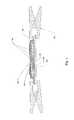
- FIG. 1is a side view cutaway diagram of an embodiment of the present invention including a deposited metallic contact with mechanical termination.
- FIG. 2is a side view cutaway diagram of an embodiment of the present invention including a deposited metallic contact with conductive adhesive-backed metallic tape termination.
- FIG. 3is a side view cutaway diagram of an embodiment of the present invention including a deposited metallic contact with conductive adhesive-backed metallic tape termination and dual-sided laminate structure.
- FIG. 4is a side view cutaway diagram of an embodiment of the present invention including a deposited metallic contact with conductive ink tack-bonding copper-coated polyimide.
- FIG. 5is a side view cutaway diagram of an embodiment of the present invention including a wire-bondable metallic contact pad.
- FIG. 6is a side view cutaway diagram of an embodiment of the present invention including a metallic via (through-hole) with back-side wire-bond-able metallic contact pad.
- a substrate ( 100 )is provided that may include a number of material, such as, for example, metal, ceramic, or plastic.
- additional layers of materialmay be provided to protect the electrochemical device. As described herein, such additional layers may be considered to be a part of the substrate ( 100 ).
- a cathode current collector (ccc)( 200 ) may be deposited upon the substrate ( 100 ).
- This ccc layermay include a metal from the group Co, Au, Ni, and Ag, or any conductor that is non-alloying with lithium.
- the ccc layersmay be deposited onto a surface using techniques such as DC sputtering or evaporation under vacuum.
- a cathodic electrode ( 300 )may be deposited over a substantial portion of the ccc layer ( 200 ).
- a material used as a cathodic electrode that may be used in the present inventionis an amorphous lithium cobalt dioxide (“LiCoO 2 ”).
- Methods of the LiCoO 2 vacuum depositionthat may be used in embodiments of the present invention may include, for example, RF sputtering.
- the LiCoO 2 cathodic electrode ( 300 )may be annealed by crystallization. Crystallization annealing may be achieved by, for example, cycling the substrate to approximately 700° C. through a gradual heating and cooling furnace process. Other means of producing the desired crystalline structure of the cathodic electrode may also be utilized.
- a metallic contact layer ( 400 )may also be isolated from previously deposited layers of the electronic device of an embodiment of the present invention for later contact to the anode.
- This metallic contact layer ( 400 )may include, for example, a metal from the group Co, Au, Ni, and Ag, or any conductor that is non-alloying with lithium.
- an electrolytic layer ( 500 )may also be deposited on the device.
- the order of deposition of contact layer ( 400 ) and electrolytic layer ( 500 )is not important.
- This electrolytic layer ( 500 ), preferably a lithium phosphorous oxynitride,is preferably deposited to substantially or approximately cover the entire ccc ( 200 ) and cathodic electrode ( 300 ) layers, and a substantial portion of the remaining surface area of the electronic device. This electrolyte coverage may extend such that subsequent metal depositions overlay it.
- RF sputteringis one preferred method of vacuum deposition of the electrolyte.
- an anode current collector (acc) ( 600 )may be deposited over a portion of the electrolytic layer ( 500 ) as depicted in FIG. 1 .
- This layermay be positioned directly above the cathode ( 300 ) region with an additional deposited tab opposed to the ccc ( 200 ) and an extension that makes contact with the metallic contact layer ( 400 ).
- This acc layermay comprise several materials including, for example, lithium.
- Methods of vacuum deposition of this layer on the appropriate surfacemay include, for example, DC sputtering or evaporation.
- a multi-layer laminate ( 700 )may be bonded to the surface of the exemplary electronic device configurations set forth above.
- This multi-layer laminate ( 700 )may include one or more of the following types of layers: sealant layer for thermal or adhesive bonding, tie layer, metallic layer, plastic or glass barrier layer, or a slip layer for outside damage protection. Bonding may be achieved by using several means including, for example, compressive force and elevated temperature in a roll laminator or vacuum bag laminator. Openings for access to the contact area may be pre-cut in the multi-layer laminate structure prior to bonding.
- a metal layerWhen a metal layer is included in the laminate of an embodiment of the present invention, it may be desirable to control the amount of depression in the laminate structure, such that shorting through the laminate does not occur. Depression control, especially at the edges, may depend on the amount of pressure applied, the temperature at which the process is performed, the conformity of the compressive surface, and the amount of time for which these forces are applied.
- a conformal materialmay be overlaid upon the multi-layer laminate structure of an embodiment of the present invention to displace air during processing.
- FIG. 1illustrates one embodiment of the present invention employing deposited metal contacts and a mechanical termination on an exemplary thin-film battery.
- a multi-layer laminate ( 700 )may be bonded to the surface of the battery with pre-cut openings over the deposited metal contact areas.
- the extended ccc ( 200 ) and the metallic contact layer ( 400 )may not have been atomically bonded to the substrate such that robust wire-bonding may be produced.
- a mechanical connector ( 800 )may be affixed to the surface of the battery. With metallic substrates, however, it may be desirable to take care when affixing a mechanical connector to avoid damaging any insulating layers.
- FIG. 2illustrates another embodiment of the present invention employing deposited metal contacts, a conductive adhesive backed metal tape, and an over-layer laminate.
- a multi-layer laminate ( 700 )may be bonded to the surface of a battery with pre-cut openings over the deposited metal contacts.
- the extended ccc ( 200 ) and the metallic contact layer ( 400 )may not have been atomically bonded to the substrate such that robust wire-bonding may be produced.
- an adhesive backed conductor tape ( 900 )may be affixed to the surface. Any such adhesive-backed conductor tape may be used including, for example, 3M 1181 EMI Shielding Tape.
- An outer encapsulant ( 1000 )may be applied to enhance the prolonged adhesion of the adhesive-backed conductor tape ( 900 ).
- the outer encapsulant layer ( 1000 )may be the same material as the multi-layer laminate ( 700 ). It may, however, be advantageous to use a simpler, more economical structure.
- FIG. 3illustrates another embodiment of the present invention employing deposited metal contacts, a conductive adhesive backed metal tape, and an over-layer laminate applied to both sides of a battery.
- a multi-layer laminate ( 700 )may be bonded to the surface of the battery with pre-cut openings over the deposited metal contacts.
- the extended ccc ( 200 ) and the metallic contact layer ( 400 )may not have been atomically bonded to the substrate so that robust wire-bonding may be produced.
- an adhesive backed conductor tape ( 900 )may be affixed to the surface. Any such adhesive-backed conductor tape may be used, including, for example, 3M 1181 EMI Shielding Tape.
- An outer encapsulant ( 1000 )may then be applied to ensure the prolonged adhesion of the adhesive-backed conductor tape ( 900 ).
- the outer encapsulant ( 1000 )may be the same material as the multi-layer laminate ( 700 ).
- a more robust packagemay be achieved by bonding to the battery surface, as described previously, and then embossing or crimping (for example thermally) the outer edges of the opposed outer encapsulant ( 1000 ) films.
- embossing or crimpingfor example thermally the outer edges of the opposed outer encapsulant ( 1000 ) films.
- caremay be taken to ensure that excessive pressure does not short to the adhesive-backed conductor tape ( 900 ) leads of the cell.
- Proper material-selection factory crimp parametersmay be utilized without cell shorting.
- the adhesive bond layer of the laminatemay also act as an insulator for the leads.
- FIG. 4illustrates yet another embodiment of the present invention employing deposited metal contacts, a copper-coated polyimide conductor strip tack-bonded with conductive ink, and the multi-layer laminate structure extended to provide strain relief or the contact.
- copper-coated polyimide ( 1100 )may be tack-bonded to the deposited metal contacts with conductive ink ( 1200 ).
- a multi-layer laminate ( 700 )may be bonded to the surface of the battery and may extend over the ink ( 1200 ) and copper-coated polyimide ( 1100 ) bond site to provide strain relief to the leads.
- FIG. 5illustrates an additional embodiment of the present invention employing deposited metal contacts contacting pre-deposited atomically bonded contacts.
- the substrate ( 100 )may be selectively coated with a conductor composition paste that may be treated to provide an atomically bonded contact ( 1300 ).
- a multi-layer laminate ( 700 )may be bonded to the surface of a battery.
- the multi-layer laminate(s)may have pre-cut openings over the atomically bonded contacts. Such contacts that are left exposed through the openings in the multi-layered laminate may be wire-bonded without further preparation.
- FIG. 6illustrates yet another embodiment of the present invention employing deposited metal contacts contacting pre-deposited metal-filled conductive through-holes.
- the deposited contactsmay contact atomically bonded contacts on the opposite side of a battery.
- the substrate ( 100 )may be prepared with holes that may be filled with metal paste, then fired to provide a conductive through path or via ( 1400 ).
- the substrate ( 100 )may be selectively coated with a conductor composition paste that may be treated to provide an atomically bonded contact ( 1300 ) on the opposite side of the substrate ( 100 ) from the deposited cell.
- a multi-layer laminate ( 700 )may be bonded to the top surface of the battery. Here, extensive pressure may be applied along the edges and there may be little risk of shorting.
Landscapes
- Chemical & Material Sciences (AREA)
- Chemical Kinetics & Catalysis (AREA)
- Electrochemistry (AREA)
- General Chemical & Material Sciences (AREA)
- Engineering & Computer Science (AREA)
- Manufacturing & Machinery (AREA)
- Inorganic Chemistry (AREA)
- Computer Hardware Design (AREA)
- Microelectronics & Electronic Packaging (AREA)
- Power Engineering (AREA)
- Connection Of Batteries Or Terminals (AREA)
- Sealing Battery Cases Or Jackets (AREA)
Abstract
Description
Claims (46)
Priority Applications (12)
| Application Number | Priority Date | Filing Date | Title |
|---|---|---|---|
| US10/215,190US6916679B2 (en) | 2002-08-09 | 2002-08-09 | Methods of and device for encapsulation and termination of electronic devices |
| US11/374,282US20080003496A1 (en) | 2002-08-09 | 2005-06-15 | Electrochemical apparatus with barrier layer protected substrate |
| US11/209,536US8021778B2 (en) | 2002-08-09 | 2005-08-23 | Electrochemical apparatus with barrier layer protected substrate |
| US11/561,277US8445130B2 (en) | 2002-08-09 | 2006-11-17 | Hybrid thin-film battery |
| US11/687,032US8236443B2 (en) | 2002-08-09 | 2007-03-16 | Metal film encapsulation |
| US12/111,388US8394522B2 (en) | 2002-08-09 | 2008-04-29 | Robust metal film encapsulation |
| US12/179,701US8431264B2 (en) | 2002-08-09 | 2008-07-25 | Hybrid thin-film battery |
| US12/545,662US7993773B2 (en) | 2002-08-09 | 2009-08-21 | Electrochemical apparatus with barrier layer protected substrate |
| US12/545,683US8535396B2 (en) | 2002-08-09 | 2009-08-21 | Electrochemical apparatus with barrier layer protected substrate |
| US12/545,673US9793523B2 (en) | 2002-08-09 | 2009-08-21 | Electrochemical apparatus with barrier layer protected substrate |
| US12/764,180US8404376B2 (en) | 2002-08-09 | 2010-04-21 | Metal film encapsulation |
| US14/191,069US9634296B2 (en) | 2002-08-09 | 2014-02-26 | Thin film battery on an integrated circuit or circuit board and method thereof |
Applications Claiming Priority (1)
| Application Number | Priority Date | Filing Date | Title |
|---|---|---|---|
| US10/215,190US6916679B2 (en) | 2002-08-09 | 2002-08-09 | Methods of and device for encapsulation and termination of electronic devices |
Related Parent Applications (1)
| Application Number | Title | Priority Date | Filing Date |
|---|---|---|---|
| US11/687,032DivisionUS8236443B2 (en) | 2002-08-09 | 2007-03-16 | Metal film encapsulation |
Related Child Applications (1)
| Application Number | Title | Priority Date | Filing Date |
|---|---|---|---|
| US11/374,282Continuation-In-PartUS20080003496A1 (en) | 2002-08-09 | 2005-06-15 | Electrochemical apparatus with barrier layer protected substrate |
Publications (2)
| Publication Number | Publication Date |
|---|---|
| US20040029311A1 US20040029311A1 (en) | 2004-02-12 |
| US6916679B2true US6916679B2 (en) | 2005-07-12 |
Family
ID=31494819
Family Applications (1)
| Application Number | Title | Priority Date | Filing Date |
|---|---|---|---|
| US10/215,190Expired - LifetimeUS6916679B2 (en) | 2002-08-09 | 2002-08-09 | Methods of and device for encapsulation and termination of electronic devices |
Country Status (1)
| Country | Link |
|---|---|
| US (1) | US6916679B2 (en) |
Cited By (62)
| Publication number | Priority date | Publication date | Assignee | Title |
|---|---|---|---|---|
| US20040214079A1 (en)* | 2003-04-22 | 2004-10-28 | Simburger Edward J. | Integrated thin film battery and circuit module |
| US20070238019A1 (en)* | 2004-08-03 | 2007-10-11 | Commissariat A L'energie Atomique | Microbattery Comprising Through-Connections and Production Method Thereof |
| WO2007106910A3 (en)* | 2006-03-16 | 2008-06-19 | Infinite Power Solution | Metal film encapsulation |
| US20090130563A1 (en)* | 2002-11-05 | 2009-05-21 | Mino Green | Structured silicon anode |
| US7557433B2 (en) | 2004-10-25 | 2009-07-07 | Mccain Joseph H | Microelectronic device with integrated energy source |
| US20100090655A1 (en)* | 2008-10-08 | 2010-04-15 | Keating Joseph A | Environmentally-Powered Wireless Sensor Module |
| US20100151324A1 (en)* | 2006-01-23 | 2010-06-17 | Mino Green | Method of fabricating fibres composed of silicon or a silicon-based material and their use in lithium rechargeable batteries |
| US20100178565A1 (en)* | 2007-07-17 | 2010-07-15 | Mino Green | Method of fabricating structured particles composed of silicon or a silicon-based material and their use in lithium rechargeable batteries |
| US20100190057A1 (en)* | 2007-07-17 | 2010-07-29 | Mino Green | Method |
| US20100196760A1 (en)* | 2007-07-17 | 2010-08-05 | Mino Green | Production |
| US20100291431A1 (en)* | 2009-05-13 | 2010-11-18 | Front Edge Technology, Inc. | Thin film battery with protective packaging |
| US20110033967A1 (en)* | 2006-06-04 | 2011-02-10 | Markus Lutz | Methods for trapping charge in a microelectromechanical system and microelectromechanical system employing same |
| US7959769B2 (en) | 2004-12-08 | 2011-06-14 | Infinite Power Solutions, Inc. | Deposition of LiCoO2 |
| US7993773B2 (en) | 2002-08-09 | 2011-08-09 | Infinite Power Solutions, Inc. | Electrochemical apparatus with barrier layer protected substrate |
| US8021778B2 (en) | 2002-08-09 | 2011-09-20 | Infinite Power Solutions, Inc. | Electrochemical apparatus with barrier layer protected substrate |
| US8062708B2 (en) | 2006-09-29 | 2011-11-22 | Infinite Power Solutions, Inc. | Masking of and material constraint for depositing battery layers on flexible substrates |
| US8197781B2 (en) | 2006-11-07 | 2012-06-12 | Infinite Power Solutions, Inc. | Sputtering target of Li3PO4 and method for producing same |
| US8236443B2 (en) | 2002-08-09 | 2012-08-07 | Infinite Power Solutions, Inc. | Metal film encapsulation |
| US8260203B2 (en) | 2008-09-12 | 2012-09-04 | Infinite Power Solutions, Inc. | Energy device with integral conductive surface for data communication via electromagnetic energy and method thereof |
| US8268488B2 (en) | 2007-12-21 | 2012-09-18 | Infinite Power Solutions, Inc. | Thin film electrolyte for thin film batteries |
| US8350519B2 (en) | 2008-04-02 | 2013-01-08 | Infinite Power Solutions, Inc | Passive over/under voltage control and protection for energy storage devices associated with energy harvesting |
| US8394522B2 (en) | 2002-08-09 | 2013-03-12 | Infinite Power Solutions, Inc. | Robust metal film encapsulation |
| US8404376B2 (en) | 2002-08-09 | 2013-03-26 | Infinite Power Solutions, Inc. | Metal film encapsulation |
| US8431264B2 (en) | 2002-08-09 | 2013-04-30 | Infinite Power Solutions, Inc. | Hybrid thin-film battery |
| US8445130B2 (en) | 2002-08-09 | 2013-05-21 | Infinite Power Solutions, Inc. | Hybrid thin-film battery |
| US8461636B2 (en) | 2006-01-26 | 2013-06-11 | Universität Linz | Ferroic sensor having tini-film field-effect transistor and ferroic layer applied to substrate |
| US8475955B2 (en) | 2005-03-25 | 2013-07-02 | Front Edge Technology, Inc. | Thin film battery with electrical connector connecting battery cells |
| US8518581B2 (en) | 2008-01-11 | 2013-08-27 | Inifinite Power Solutions, Inc. | Thin film encapsulation for thin film batteries and other devices |
| US8585918B2 (en) | 2006-01-23 | 2013-11-19 | Nexeon Ltd. | Method of etching a silicon-based material |
| US8599572B2 (en) | 2009-09-01 | 2013-12-03 | Infinite Power Solutions, Inc. | Printed circuit board with integrated thin film battery |
| US8636876B2 (en) | 2004-12-08 | 2014-01-28 | R. Ernest Demaray | Deposition of LiCoO2 |
| US8679674B2 (en) | 2005-03-25 | 2014-03-25 | Front Edge Technology, Inc. | Battery with protective packaging |
| US8728285B2 (en) | 2003-05-23 | 2014-05-20 | Demaray, Llc | Transparent conductive oxides |
| US8753724B2 (en) | 2012-09-26 | 2014-06-17 | Front Edge Technology Inc. | Plasma deposition on a partially formed battery through a mesh screen |
| US8772174B2 (en) | 2010-04-09 | 2014-07-08 | Nexeon Ltd. | Method of fabricating structured particles composed of silicon or silicon-based material and their use in lithium rechargeable batteries |
| US8864954B2 (en) | 2011-12-23 | 2014-10-21 | Front Edge Technology Inc. | Sputtering lithium-containing material with multiple targets |
| US8865340B2 (en) | 2011-10-20 | 2014-10-21 | Front Edge Technology Inc. | Thin film battery packaging formed by localized heating |
| US8906523B2 (en) | 2008-08-11 | 2014-12-09 | Infinite Power Solutions, Inc. | Energy device with integral collector surface for electromagnetic energy harvesting and method thereof |
| US8932759B2 (en) | 2008-10-10 | 2015-01-13 | Nexeon Ltd. | Method of fabricating structured particles composed of silicon or a silicon-based material |
| US8945774B2 (en) | 2010-06-07 | 2015-02-03 | Nexeon Ltd. | Additive for lithium ion rechageable battery cells |
| US8962183B2 (en) | 2009-05-07 | 2015-02-24 | Nexeon Limited | Method of making silicon anode material for rechargeable cells |
| CN104679975A (en)* | 2012-12-26 | 2015-06-03 | 迪士尼企业公司 | Unlocking content and/or effectuating modifications in virtual space instances presented via multiple computing platforms |
| US9077000B2 (en) | 2012-03-29 | 2015-07-07 | Front Edge Technology, Inc. | Thin film battery and localized heat treatment |
| US9184438B2 (en) | 2008-10-10 | 2015-11-10 | Nexeon Ltd. | Method of fabricating structured particles composed of silicon or a silicon-based material and their use in lithium rechargeable batteries |
| US9252426B2 (en) | 2007-05-11 | 2016-02-02 | Nexeon Limited | Silicon anode for a rechargeable battery |
| US9257695B2 (en) | 2012-03-29 | 2016-02-09 | Front Edge Technology, Inc. | Localized heat treatment of battery component films |
| US9334557B2 (en) | 2007-12-21 | 2016-05-10 | Sapurast Research Llc | Method for sputter targets for electrolyte films |
| US9356320B2 (en) | 2012-10-15 | 2016-05-31 | Front Edge Technology Inc. | Lithium battery having low leakage anode |
| US9608272B2 (en) | 2009-05-11 | 2017-03-28 | Nexeon Limited | Composition for a secondary battery cell |
| US9634296B2 (en) | 2002-08-09 | 2017-04-25 | Sapurast Research Llc | Thin film battery on an integrated circuit or circuit board and method thereof |
| US9647263B2 (en) | 2010-09-03 | 2017-05-09 | Nexeon Limited | Electroactive material |
| US9853292B2 (en) | 2009-05-11 | 2017-12-26 | Nexeon Limited | Electrode composition for a secondary battery cell |
| US9871248B2 (en) | 2010-09-03 | 2018-01-16 | Nexeon Limited | Porous electroactive material |
| US9887429B2 (en) | 2011-12-21 | 2018-02-06 | Front Edge Technology Inc. | Laminated lithium battery |
| US9905895B2 (en) | 2012-09-25 | 2018-02-27 | Front Edge Technology, Inc. | Pulsed mode apparatus with mismatched battery |
| US9911696B2 (en)* | 2007-07-09 | 2018-03-06 | Micron Technology, Inc. | Packaged semiconductor assemblies and methods for manufacturing such assemblies |
| US9922185B2 (en) | 2012-12-26 | 2018-03-20 | Disney Enterprises, Inc. | Linking token detection at a single computing platform with a user identification to effectuate modifications in virtual space instances presented via multiple computing platforms |
| US10008739B2 (en) | 2015-02-23 | 2018-06-26 | Front Edge Technology, Inc. | Solid-state lithium battery with electrolyte |
| US20200136102A1 (en)* | 2018-10-25 | 2020-04-30 | Samsung Electronics Co., Ltd. | Secondary battery removably attachable to power module, and electronic apparatus including the same |
| US10680277B2 (en) | 2010-06-07 | 2020-06-09 | Sapurast Research Llc | Rechargeable, high-density electrochemical device |
| US10957886B2 (en) | 2018-03-14 | 2021-03-23 | Front Edge Technology, Inc. | Battery having multilayer protective casing |
| US11322787B2 (en) | 2019-11-18 | 2022-05-03 | International Business Machines Corporation | Encapsulating in-situ energy storage device with cathode contact |
Families Citing this family (44)
| Publication number | Priority date | Publication date | Assignee | Title |
|---|---|---|---|---|
| ES2350350T3 (en)* | 2004-07-02 | 2011-01-21 | Konarka Technologies, Inc. | ORGANIC PHOTOVOLTAIC COMPONENT WITH ENCAPSULATION. |
| US8732004B1 (en) | 2004-09-22 | 2014-05-20 | Experian Information Solutions, Inc. | Automated analysis of data to generate prospect notifications based on trigger events |
| US7792732B2 (en) | 2004-10-29 | 2010-09-07 | American Express Travel Related Services Company, Inc. | Using commercial share of wallet to rate investments |
| US7524577B2 (en)* | 2005-09-06 | 2009-04-28 | Oak Ridge Micro-Energy, Inc. | Long life thin film battery and method therefor |
| US20080221971A1 (en)* | 2005-10-24 | 2008-09-11 | Megdal Myles G | Using commercial share of wallet to rate business prospects |
| US20080243680A1 (en)* | 2005-10-24 | 2008-10-02 | Megdal Myles G | Method and apparatus for rating asset-backed securities |
| US20080033852A1 (en)* | 2005-10-24 | 2008-02-07 | Megdal Myles G | Computer-based modeling of spending behaviors of entities |
| US20080221973A1 (en)* | 2005-10-24 | 2008-09-11 | Megdal Myles G | Using commercial share of wallet to rate investments |
| US20080228541A1 (en)* | 2005-10-24 | 2008-09-18 | Megdal Myles G | Using commercial share of wallet in private equity investments |
| US20080228540A1 (en)* | 2005-10-24 | 2008-09-18 | Megdal Myles G | Using commercial share of wallet to compile marketing company lists |
| JP5300187B2 (en)* | 2006-09-07 | 2013-09-25 | 三洋電機株式会社 | Pack battery charged by magnetic induction |
| US8036979B1 (en) | 2006-10-05 | 2011-10-11 | Experian Information Solutions, Inc. | System and method for generating a finance attribute from tradeline data |
| US8606626B1 (en) | 2007-01-31 | 2013-12-10 | Experian Information Solutions, Inc. | Systems and methods for providing a direct marketing campaign planning environment |
| US8606666B1 (en) | 2007-01-31 | 2013-12-10 | Experian Information Solutions, Inc. | System and method for providing an aggregation tool |
| WO2008100441A2 (en)* | 2007-02-09 | 2008-08-21 | Cymbet Corporation | Charging systems and methods |
| FR2925227B1 (en)* | 2007-12-12 | 2009-11-27 | Commissariat Energie Atomique | ENCASPULATED LITHIUM ELECTROCHEMICAL DEVICE. |
| KR101831401B1 (en)* | 2010-01-26 | 2018-02-23 | 사임베트 코퍼레이션 | Battery arrays, construction and method |
| US9652802B1 (en) | 2010-03-24 | 2017-05-16 | Consumerinfo.Com, Inc. | Indirect monitoring and reporting of a user's credit data |
| EP2754194B1 (en) | 2011-09-07 | 2018-12-12 | 24M Technologies, Inc. | Semi-solid electrode cell having a porous current collector and methods of manufacture |
| KR101305660B1 (en)* | 2011-10-17 | 2013-09-09 | 엘지이노텍 주식회사 | Solar cell module and method of fabricating the same |
| FR2987173A1 (en)* | 2012-02-17 | 2013-08-23 | St Microelectronics Tours Sas | METHOD FOR PRODUCING A MICROBATTERY |
| US9178200B2 (en)* | 2012-05-18 | 2015-11-03 | 24M Technologies, Inc. | Electrochemical cells and methods of manufacturing the same |
| US9401501B2 (en) | 2012-05-18 | 2016-07-26 | 24M Technologies, Inc. | Electrochemical cells and methods of manufacturing the same |
| US20140199572A1 (en)* | 2013-01-17 | 2014-07-17 | Sensormatic Electronics, LLC | Film-based battery holder |
| FR3010832B1 (en) | 2013-09-16 | 2017-12-15 | Commissariat Energie Atomique | PROCESS FOR PRODUCING LITHIUM MICROBATTERIUM |
| US10262362B1 (en) | 2014-02-14 | 2019-04-16 | Experian Information Solutions, Inc. | Automatic generation of code for attributes |
| CN106463658A (en) | 2014-06-23 | 2017-02-22 | 肖特股份有限公司 | Electric storage system including sheet-like discontinuous element, sheet-like discontinuous element, manufacturing method and application thereof |
| US9793522B2 (en)* | 2014-08-13 | 2017-10-17 | Verily Life Sciences Llc | Sealed solid state battery |
| ES2975858T3 (en) | 2014-10-13 | 2024-07-16 | 24M Tech Inc | Systems and methods of charging and forming batteries in series |
| KR102286337B1 (en)* | 2014-10-17 | 2021-08-04 | 쓰리엠 이노베이티브 프로퍼티즈 컴파니 | Emi shielding structure and thermal pad, and electronic circuit board assembly including the same |
| KR102793671B1 (en) | 2014-11-05 | 2025-04-10 | 24엠 테크놀로지즈, 인크. | Electrochemical cells having semi-solid electrodes and methods of manufacturing the same |
| WO2016087311A2 (en) | 2014-12-01 | 2016-06-09 | Schott Ag | Electrical storage system comprising a sheet-type discrete element, discrete sheet-type element, method for the production thereof and use thereof |
| US10445152B1 (en) | 2014-12-19 | 2019-10-15 | Experian Information Solutions, Inc. | Systems and methods for dynamic report generation based on automatic modeling of complex data structures |
| WO2016205663A1 (en) | 2015-06-18 | 2016-12-22 | 24M Technologies, Inc. | Single pouch battery cells and methods of manufacture |
| US9821541B2 (en)* | 2015-07-14 | 2017-11-21 | uBeam Inc. | Laminate material bonding |
| US9728494B2 (en) | 2015-09-24 | 2017-08-08 | Verily Life Sciences Llc | Body-mountable device with a common substrate for electronics and battery |
| US20170301892A1 (en)* | 2016-04-14 | 2017-10-19 | Applied Materials, Inc. | Multilayer thin film device encapsulation using soft and pliable layer first |
| FR3078200B1 (en)* | 2018-02-16 | 2020-03-20 | Commissariat A L'energie Atomique Et Aux Energies Alternatives | PROCESS FOR MANUFACTURING A POSITIVE ELECTRODE FOR ANY SOLID LITHIUM MICROBATTERY |
| US20210091372A1 (en)* | 2019-09-23 | 2021-03-25 | International Business Machines Corporation | High capacity compact lithium thin film battery |
| CN112993450B (en)* | 2019-12-18 | 2023-06-09 | 卡西欧计算机株式会社 | Lithium battery, lithium battery module and electronic equipment |
| US11742525B2 (en) | 2020-02-07 | 2023-08-29 | 24M Technologies, Inc. | Divided energy electrochemical cell systems and methods of producing the same |
| US12381277B2 (en) | 2020-06-17 | 2025-08-05 | 24M Technologies, Inc. | Electrochemical cells with flame retardant mechanism and methods of producing the same |
| DE102020209181A1 (en) | 2020-07-22 | 2022-01-27 | Robert Bosch Gesellschaft mit beschränkter Haftung | Battery module and method of manufacturing the same |
| CN112490492A (en)* | 2020-11-27 | 2021-03-12 | 珠海冠宇动力电池有限公司 | Lithium ion battery and manufacturing method thereof |
Citations (39)
| Publication number | Priority date | Publication date | Assignee | Title |
|---|---|---|---|---|
| US4127424A (en)* | 1976-12-06 | 1978-11-28 | Ses, Incorporated | Photovoltaic cell array |
| US4481265A (en)* | 1982-06-11 | 1984-11-06 | Hitachi, Ltd. | Photovoltaic-storage battery device |
| JPS6068558A (en) | 1983-09-26 | 1985-04-19 | Hitachi Ltd | All solid state thin film lithium battery |
| US4555456A (en) | 1983-05-26 | 1985-11-26 | Hitachi, Ltd. | Cathode structure for thin film battery |
| US4740431A (en)* | 1986-12-22 | 1988-04-26 | Spice Corporation | Integrated solar cell and battery |
| US5110696A (en) | 1990-11-09 | 1992-05-05 | Bell Communications Research | Rechargeable lithiated thin film intercalation electrode battery |
| US5171413A (en) | 1991-09-16 | 1992-12-15 | Tufts University | Methods for manufacturing solid state ionic devices |
| US5338625A (en) | 1992-07-29 | 1994-08-16 | Martin Marietta Energy Systems, Inc. | Thin film battery and method for making same |
| US5411592A (en) | 1994-06-06 | 1995-05-02 | Ovonic Battery Company, Inc. | Apparatus for deposition of thin-film, solid state batteries |
| US5445906A (en) | 1994-08-03 | 1995-08-29 | Martin Marietta Energy Systems, Inc. | Method and system for constructing a rechargeable battery and battery structures formed with the method |
| US5470396A (en)* | 1994-04-12 | 1995-11-28 | Amoco Corporation | Solar cell module package and method for its preparation |
| US5512389A (en) | 1994-11-02 | 1996-04-30 | Dasgupta; Sankar | Rechargeable non-aqueous thin film lithium battery |
| US5552242A (en) | 1993-11-19 | 1996-09-03 | Ovonic Battery Company, Inc. | Solid state battery using a hydrogenated silicon nitride electrolyte |
| US5561004A (en) | 1994-02-25 | 1996-10-01 | Bates; John B. | Packaging material for thin film lithium batteries |
| US5599355A (en) | 1993-08-20 | 1997-02-04 | Nagasubramanian; Ganesan | Method for forming thin composite solid electrolyte film for lithium batteries |
| US5645960A (en) | 1995-05-19 | 1997-07-08 | The United States Of America As Represented By The Secretary Of The Air Force | Thin film lithium polymer battery |
| US5705293A (en) | 1997-01-09 | 1998-01-06 | Lockheed Martin Energy Research Corporation | Solid state thin film battery having a high temperature lithium alloy anode |
| US5755940A (en) | 1994-06-13 | 1998-05-26 | Mitsui Petrochemical Industries, Ltd. | Lithium ionic conducting glass thin film and carbon dioxide sensor comprising the glass thin film |
| WO1998047196A1 (en) | 1997-04-16 | 1998-10-22 | Lockheed Martin Energy Systems, Inc. | Silicon-tin oxynitride glassy composition and use as anode for lithium-ion battery |
| US5834137A (en) | 1995-10-06 | 1998-11-10 | Midwest Research Institute | Thin film method of conducting lithium-ions |
| US5895731A (en) | 1997-05-15 | 1999-04-20 | Nelson E. Smith | Thin-film lithium battery and process |
| US5961672A (en) | 1994-02-16 | 1999-10-05 | Moltech Corporation | Stabilized anode for lithium-polymer batteries |
| US6030421A (en)* | 1997-04-23 | 2000-02-29 | Hydro-Quebec | Ultra thin solid state lithium batteries and process of preparing same |
| US6045942A (en)* | 1997-12-15 | 2000-04-04 | Avery Dennison Corporation | Low profile battery and method of making same |
| US6080508A (en) | 1998-03-06 | 2000-06-27 | Electrofuel Inc. | Packaging assembly for a lithium battery |
| US6120890A (en) | 1997-12-12 | 2000-09-19 | Seagate Technology, Inc. | Magnetic thin film medium comprising amorphous sealing layer for reduced lithium migration |
| WO2000060682A1 (en) | 1999-04-02 | 2000-10-12 | Excellatron Solid State, Llc | Thin lithium film battery |
| US6168884B1 (en) | 1999-04-02 | 2001-01-02 | Lockheed Martin Energy Research Corporation | Battery with an in-situ activation plated lithium anode |
| US6175075B1 (en)* | 1998-04-21 | 2001-01-16 | Canon Kabushiki Kaisha | Solar cell module excelling in reliability |
| WO2001017052A2 (en) | 1999-09-02 | 2001-03-08 | Lithium Power Technologies, Inc. | All-solid-state electrochemical device and method of manufacturing |
| US6280875B1 (en) | 1999-03-24 | 2001-08-28 | Teledyne Technologies Incorporated | Rechargeable battery structure with metal substrate |
| US6323416B1 (en)* | 1996-09-12 | 2001-11-27 | Canon Kabushiki Kaisha | Solar cell module |
| US6369316B1 (en)* | 1998-07-03 | 2002-04-09 | ISOVOLTA Österreichische Isolierstoffwerke Aktiengesellschaft | Photovoltaic module and method for producing same |
| US6376027B1 (en) | 2000-05-01 | 2002-04-23 | Korea Advanced Institute Of Science And Technology | Method for crystallizing lithium transition metal oxide thin film by plasma treatment |
| US6380477B1 (en)* | 1999-03-26 | 2002-04-30 | Lawrence F. Curtin | Method of making photovoltaic device |
| US6413285B1 (en)* | 1999-11-01 | 2002-07-02 | Polyplus Battery Company | Layered arrangements of lithium electrodes |
| US20030029493A1 (en)* | 2000-03-09 | 2003-02-13 | Albert Plessing | Method for producing photovoltaic thin film module |
| US20030091904A1 (en)* | 1999-06-28 | 2003-05-15 | Lithium Power Technologies, Inc. | Ionically conductive polymer electrolytes |
| US20030109903A1 (en)* | 2001-12-12 | 2003-06-12 | Epic Biosonics Inc. | Low profile subcutaneous enclosure |
Family Cites Families (1)
| Publication number | Priority date | Publication date | Assignee | Title |
|---|---|---|---|---|
| US5690703A (en)* | 1996-03-15 | 1997-11-25 | Valence Technology, Inc | Apparatus and method of preparing electrochemical cells |
- 2002
- 2002-08-09USUS10/215,190patent/US6916679B2/ennot_activeExpired - Lifetime
Patent Citations (45)
| Publication number | Priority date | Publication date | Assignee | Title |
|---|---|---|---|---|
| US4127424A (en)* | 1976-12-06 | 1978-11-28 | Ses, Incorporated | Photovoltaic cell array |
| US4481265A (en)* | 1982-06-11 | 1984-11-06 | Hitachi, Ltd. | Photovoltaic-storage battery device |
| US4555456A (en) | 1983-05-26 | 1985-11-26 | Hitachi, Ltd. | Cathode structure for thin film battery |
| JPS6068558A (en) | 1983-09-26 | 1985-04-19 | Hitachi Ltd | All solid state thin film lithium battery |
| US4740431A (en)* | 1986-12-22 | 1988-04-26 | Spice Corporation | Integrated solar cell and battery |
| US5110696A (en) | 1990-11-09 | 1992-05-05 | Bell Communications Research | Rechargeable lithiated thin film intercalation electrode battery |
| US5171413A (en) | 1991-09-16 | 1992-12-15 | Tufts University | Methods for manufacturing solid state ionic devices |
| US5512147A (en) | 1992-07-29 | 1996-04-30 | Martin Marietta Energy Systems, Inc. | Method of making an electrolyte for an electrochemical cell |
| US6218049B1 (en) | 1992-07-29 | 2001-04-17 | Ut-Battelle, Llc | Cathode for an electrochemical cell |
| US5338625A (en) | 1992-07-29 | 1994-08-16 | Martin Marietta Energy Systems, Inc. | Thin film battery and method for making same |
| US5567210A (en) | 1992-07-29 | 1996-10-22 | Martin Marietta Energy Systems, Inc. | Method for making an electrochemical cell |
| US5599355A (en) | 1993-08-20 | 1997-02-04 | Nagasubramanian; Ganesan | Method for forming thin composite solid electrolyte film for lithium batteries |
| US5552242A (en) | 1993-11-19 | 1996-09-03 | Ovonic Battery Company, Inc. | Solid state battery using a hydrogenated silicon nitride electrolyte |
| US5961672A (en) | 1994-02-16 | 1999-10-05 | Moltech Corporation | Stabilized anode for lithium-polymer batteries |
| US5561004A (en) | 1994-02-25 | 1996-10-01 | Bates; John B. | Packaging material for thin film lithium batteries |
| US5470396A (en)* | 1994-04-12 | 1995-11-28 | Amoco Corporation | Solar cell module package and method for its preparation |
| US5411592A (en) | 1994-06-06 | 1995-05-02 | Ovonic Battery Company, Inc. | Apparatus for deposition of thin-film, solid state batteries |
| US5755940A (en) | 1994-06-13 | 1998-05-26 | Mitsui Petrochemical Industries, Ltd. | Lithium ionic conducting glass thin film and carbon dioxide sensor comprising the glass thin film |
| US5445906A (en) | 1994-08-03 | 1995-08-29 | Martin Marietta Energy Systems, Inc. | Method and system for constructing a rechargeable battery and battery structures formed with the method |
| US5512389A (en) | 1994-11-02 | 1996-04-30 | Dasgupta; Sankar | Rechargeable non-aqueous thin film lithium battery |
| US5645960A (en) | 1995-05-19 | 1997-07-08 | The United States Of America As Represented By The Secretary Of The Air Force | Thin film lithium polymer battery |
| US5834137A (en) | 1995-10-06 | 1998-11-10 | Midwest Research Institute | Thin film method of conducting lithium-ions |
| US20010054437A1 (en)* | 1996-09-12 | 2001-12-27 | Ayako Komori | Solar cell module |
| US6323416B1 (en)* | 1996-09-12 | 2001-11-27 | Canon Kabushiki Kaisha | Solar cell module |
| US5705293A (en) | 1997-01-09 | 1998-01-06 | Lockheed Martin Energy Research Corporation | Solid state thin film battery having a high temperature lithium alloy anode |
| WO1998047196A1 (en) | 1997-04-16 | 1998-10-22 | Lockheed Martin Energy Systems, Inc. | Silicon-tin oxynitride glassy composition and use as anode for lithium-ion battery |
| US6030421A (en)* | 1997-04-23 | 2000-02-29 | Hydro-Quebec | Ultra thin solid state lithium batteries and process of preparing same |
| US5895731A (en) | 1997-05-15 | 1999-04-20 | Nelson E. Smith | Thin-film lithium battery and process |
| US6120890A (en) | 1997-12-12 | 2000-09-19 | Seagate Technology, Inc. | Magnetic thin film medium comprising amorphous sealing layer for reduced lithium migration |
| US6045942A (en)* | 1997-12-15 | 2000-04-04 | Avery Dennison Corporation | Low profile battery and method of making same |
| US6080508A (en) | 1998-03-06 | 2000-06-27 | Electrofuel Inc. | Packaging assembly for a lithium battery |
| US6175075B1 (en)* | 1998-04-21 | 2001-01-16 | Canon Kabushiki Kaisha | Solar cell module excelling in reliability |
| US6369316B1 (en)* | 1998-07-03 | 2002-04-09 | ISOVOLTA Österreichische Isolierstoffwerke Aktiengesellschaft | Photovoltaic module and method for producing same |
| US6280875B1 (en) | 1999-03-24 | 2001-08-28 | Teledyne Technologies Incorporated | Rechargeable battery structure with metal substrate |
| US6380477B1 (en)* | 1999-03-26 | 2002-04-30 | Lawrence F. Curtin | Method of making photovoltaic device |
| US6242129B1 (en) | 1999-04-02 | 2001-06-05 | Excellatron Solid State, Llc | Thin lithium film battery |
| US6168884B1 (en) | 1999-04-02 | 2001-01-02 | Lockheed Martin Energy Research Corporation | Battery with an in-situ activation plated lithium anode |
| WO2000060682A1 (en) | 1999-04-02 | 2000-10-12 | Excellatron Solid State, Llc | Thin lithium film battery |
| US20030091904A1 (en)* | 1999-06-28 | 2003-05-15 | Lithium Power Technologies, Inc. | Ionically conductive polymer electrolytes |
| WO2001017052A2 (en) | 1999-09-02 | 2001-03-08 | Lithium Power Technologies, Inc. | All-solid-state electrochemical device and method of manufacturing |
| US6664006B1 (en)* | 1999-09-02 | 2003-12-16 | Lithium Power Technologies, Inc. | All-solid-state electrochemical device and method of manufacturing |
| US6413285B1 (en)* | 1999-11-01 | 2002-07-02 | Polyplus Battery Company | Layered arrangements of lithium electrodes |
| US20030029493A1 (en)* | 2000-03-09 | 2003-02-13 | Albert Plessing | Method for producing photovoltaic thin film module |
| US6376027B1 (en) | 2000-05-01 | 2002-04-23 | Korea Advanced Institute Of Science And Technology | Method for crystallizing lithium transition metal oxide thin film by plasma treatment |
| US20030109903A1 (en)* | 2001-12-12 | 2003-06-12 | Epic Biosonics Inc. | Low profile subcutaneous enclosure |
Cited By (94)
| Publication number | Priority date | Publication date | Assignee | Title |
|---|---|---|---|---|
| US8535396B2 (en) | 2002-08-09 | 2013-09-17 | Infinite Power Solutions, Inc. | Electrochemical apparatus with barrier layer protected substrate |
| US8394522B2 (en) | 2002-08-09 | 2013-03-12 | Infinite Power Solutions, Inc. | Robust metal film encapsulation |
| US8404376B2 (en) | 2002-08-09 | 2013-03-26 | Infinite Power Solutions, Inc. | Metal film encapsulation |
| US9793523B2 (en) | 2002-08-09 | 2017-10-17 | Sapurast Research Llc | Electrochemical apparatus with barrier layer protected substrate |
| US8431264B2 (en) | 2002-08-09 | 2013-04-30 | Infinite Power Solutions, Inc. | Hybrid thin-film battery |
| US8236443B2 (en) | 2002-08-09 | 2012-08-07 | Infinite Power Solutions, Inc. | Metal film encapsulation |
| US8445130B2 (en) | 2002-08-09 | 2013-05-21 | Infinite Power Solutions, Inc. | Hybrid thin-film battery |
| US9634296B2 (en) | 2002-08-09 | 2017-04-25 | Sapurast Research Llc | Thin film battery on an integrated circuit or circuit board and method thereof |
| US8021778B2 (en) | 2002-08-09 | 2011-09-20 | Infinite Power Solutions, Inc. | Electrochemical apparatus with barrier layer protected substrate |
| US7993773B2 (en) | 2002-08-09 | 2011-08-09 | Infinite Power Solutions, Inc. | Electrochemical apparatus with barrier layer protected substrate |
| US7842535B2 (en) | 2002-11-05 | 2010-11-30 | Nexeon Ltd. | Structured silicon anode |
| US8017430B2 (en) | 2002-11-05 | 2011-09-13 | Nexeon Ltd. | Structured silicon anode |
| US20090130563A1 (en)* | 2002-11-05 | 2009-05-21 | Mino Green | Structured silicon anode |
| US8384058B2 (en) | 2002-11-05 | 2013-02-26 | Nexeon Ltd. | Structured silicon anode |
| US7683359B2 (en) | 2002-11-05 | 2010-03-23 | Nexeon Ltd. | Structured silicon anode |
| US20110107590A1 (en)* | 2002-11-05 | 2011-05-12 | Nexeon Limited | Structured silicon anode |
| US7045246B2 (en)* | 2003-04-22 | 2006-05-16 | The Aerospace Corporation | Integrated thin film battery and circuit module |
| US20040214079A1 (en)* | 2003-04-22 | 2004-10-28 | Simburger Edward J. | Integrated thin film battery and circuit module |
| US8728285B2 (en) | 2003-05-23 | 2014-05-20 | Demaray, Llc | Transparent conductive oxides |
| US9099410B2 (en) | 2003-10-13 | 2015-08-04 | Joseph H. McCain | Microelectronic device with integrated energy source |
| US9413405B2 (en) | 2003-10-13 | 2016-08-09 | Joseph H. McCain | Microelectronic device with integrated energy source |
| US20070238019A1 (en)* | 2004-08-03 | 2007-10-11 | Commissariat A L'energie Atomique | Microbattery Comprising Through-Connections and Production Method Thereof |
| US7811702B2 (en)* | 2004-08-03 | 2010-10-12 | Commissariat à l'Energie Atomique | Microbattery comprising through-connections and production method thereof |
| US7557433B2 (en) | 2004-10-25 | 2009-07-07 | Mccain Joseph H | Microelectronic device with integrated energy source |
| US7959769B2 (en) | 2004-12-08 | 2011-06-14 | Infinite Power Solutions, Inc. | Deposition of LiCoO2 |
| US8636876B2 (en) | 2004-12-08 | 2014-01-28 | R. Ernest Demaray | Deposition of LiCoO2 |
| US8475955B2 (en) | 2005-03-25 | 2013-07-02 | Front Edge Technology, Inc. | Thin film battery with electrical connector connecting battery cells |
| US8679674B2 (en) | 2005-03-25 | 2014-03-25 | Front Edge Technology, Inc. | Battery with protective packaging |
| EP2426753A1 (en) | 2005-06-15 | 2012-03-07 | Infinite Power Solutions, Inc. | Electrochemical apparatus with barrier layer protected substrate |
| US8101298B2 (en) | 2006-01-23 | 2012-01-24 | Nexeon Ltd. | Method of fabricating fibres composed of silicon or a silicon-based material and their use in lithium rechargeable batteries |
| US9583762B2 (en) | 2006-01-23 | 2017-02-28 | Nexeon Limited | Method of fabricating fibres composed of silicon or a silicon-based material and their use in lithium rechargeable batteries |
| US20100151324A1 (en)* | 2006-01-23 | 2010-06-17 | Mino Green | Method of fabricating fibres composed of silicon or a silicon-based material and their use in lithium rechargeable batteries |
| US8597831B2 (en) | 2006-01-23 | 2013-12-03 | Nexeon Ltd. | Method of fabricating fibres composed of silicon or a silicon-based material and their use in lithium rechargeable batteries |
| US8585918B2 (en) | 2006-01-23 | 2013-11-19 | Nexeon Ltd. | Method of etching a silicon-based material |
| US8461636B2 (en) | 2006-01-26 | 2013-06-11 | Universität Linz | Ferroic sensor having tini-film field-effect transistor and ferroic layer applied to substrate |
| WO2007106910A3 (en)* | 2006-03-16 | 2008-06-19 | Infinite Power Solution | Metal film encapsulation |
| US20110033967A1 (en)* | 2006-06-04 | 2011-02-10 | Markus Lutz | Methods for trapping charge in a microelectromechanical system and microelectromechanical system employing same |
| US8343790B2 (en)* | 2006-06-04 | 2013-01-01 | Robert Bosch Gmbh | Methods for trapping charge in a microelectromechanical system and microelectromechanical system employing same |
| US8766706B2 (en) | 2006-06-04 | 2014-07-01 | Robert Bosch Gmbh | Methods for trapping charge in a microelectromechanical system and microelectromechanical system employing same |
| US8062708B2 (en) | 2006-09-29 | 2011-11-22 | Infinite Power Solutions, Inc. | Masking of and material constraint for depositing battery layers on flexible substrates |
| US8197781B2 (en) | 2006-11-07 | 2012-06-12 | Infinite Power Solutions, Inc. | Sputtering target of Li3PO4 and method for producing same |
| US9871249B2 (en) | 2007-05-11 | 2018-01-16 | Nexeon Limited | Silicon anode for a rechargeable battery |
| US9252426B2 (en) | 2007-05-11 | 2016-02-02 | Nexeon Limited | Silicon anode for a rechargeable battery |
| US9911696B2 (en)* | 2007-07-09 | 2018-03-06 | Micron Technology, Inc. | Packaged semiconductor assemblies and methods for manufacturing such assemblies |
| US10622308B2 (en) | 2007-07-09 | 2020-04-14 | Micron Technology, Inc. | Packaged semiconductor assemblies and methods for manufacturing such assemblies |
| US8642211B2 (en) | 2007-07-17 | 2014-02-04 | Nexeon Limited | Electrode including silicon-comprising fibres and electrochemical cells including the same |
| US20100196760A1 (en)* | 2007-07-17 | 2010-08-05 | Mino Green | Production |
| US20100190057A1 (en)* | 2007-07-17 | 2010-07-29 | Mino Green | Method |
| US9871244B2 (en) | 2007-07-17 | 2018-01-16 | Nexeon Limited | Method of fabricating structured particles composed of silicon or a silicon-based material and their use in lithium rechargeable batteries |
| US8940437B2 (en) | 2007-07-17 | 2015-01-27 | Nexeon Limited | Method of fabricating structured particles composed of silicon or a silicon-based material and their use in lithium rechargeable batteries |
| US9012079B2 (en) | 2007-07-17 | 2015-04-21 | Nexeon Ltd | Electrode comprising structured silicon-based material |
| US8870975B2 (en) | 2007-07-17 | 2014-10-28 | Nexeon Ltd. | Method of fabricating structured particles composed of silicon or a silicon-based material and their use in lithium rechargeable batteries |
| US20100178565A1 (en)* | 2007-07-17 | 2010-07-15 | Mino Green | Method of fabricating structured particles composed of silicon or a silicon-based material and their use in lithium rechargeable batteries |
| US9334557B2 (en) | 2007-12-21 | 2016-05-10 | Sapurast Research Llc | Method for sputter targets for electrolyte films |
| US8268488B2 (en) | 2007-12-21 | 2012-09-18 | Infinite Power Solutions, Inc. | Thin film electrolyte for thin film batteries |
| US8518581B2 (en) | 2008-01-11 | 2013-08-27 | Inifinite Power Solutions, Inc. | Thin film encapsulation for thin film batteries and other devices |
| US9786873B2 (en) | 2008-01-11 | 2017-10-10 | Sapurast Research Llc | Thin film encapsulation for thin film batteries and other devices |
| US9029012B2 (en) | 2008-01-11 | 2015-05-12 | Sapurast Research Llc | Thin film encapsulation for thin film batteries and other devices |
| US8350519B2 (en) | 2008-04-02 | 2013-01-08 | Infinite Power Solutions, Inc | Passive over/under voltage control and protection for energy storage devices associated with energy harvesting |
| US8906523B2 (en) | 2008-08-11 | 2014-12-09 | Infinite Power Solutions, Inc. | Energy device with integral collector surface for electromagnetic energy harvesting and method thereof |
| US8260203B2 (en) | 2008-09-12 | 2012-09-04 | Infinite Power Solutions, Inc. | Energy device with integral conductive surface for data communication via electromagnetic energy and method thereof |
| US20100090655A1 (en)* | 2008-10-08 | 2010-04-15 | Keating Joseph A | Environmentally-Powered Wireless Sensor Module |
| US8508193B2 (en) | 2008-10-08 | 2013-08-13 | Infinite Power Solutions, Inc. | Environmentally-powered wireless sensor module |
| US9184438B2 (en) | 2008-10-10 | 2015-11-10 | Nexeon Ltd. | Method of fabricating structured particles composed of silicon or a silicon-based material and their use in lithium rechargeable batteries |
| US8932759B2 (en) | 2008-10-10 | 2015-01-13 | Nexeon Ltd. | Method of fabricating structured particles composed of silicon or a silicon-based material |
| US8962183B2 (en) | 2009-05-07 | 2015-02-24 | Nexeon Limited | Method of making silicon anode material for rechargeable cells |
| US9553304B2 (en) | 2009-05-07 | 2017-01-24 | Nexeon Limited | Method of making silicon anode material for rechargeable cells |
| US9853292B2 (en) | 2009-05-11 | 2017-12-26 | Nexeon Limited | Electrode composition for a secondary battery cell |
| US9608272B2 (en) | 2009-05-11 | 2017-03-28 | Nexeon Limited | Composition for a secondary battery cell |
| US10050275B2 (en) | 2009-05-11 | 2018-08-14 | Nexeon Limited | Binder for lithium ion rechargeable battery cells |
| US20100291431A1 (en)* | 2009-05-13 | 2010-11-18 | Front Edge Technology, Inc. | Thin film battery with protective packaging |
| US9532453B2 (en) | 2009-09-01 | 2016-12-27 | Sapurast Research Llc | Printed circuit board with integrated thin film battery |
| US8599572B2 (en) | 2009-09-01 | 2013-12-03 | Infinite Power Solutions, Inc. | Printed circuit board with integrated thin film battery |
| US8772174B2 (en) | 2010-04-09 | 2014-07-08 | Nexeon Ltd. | Method of fabricating structured particles composed of silicon or silicon-based material and their use in lithium rechargeable batteries |
| US10680277B2 (en) | 2010-06-07 | 2020-06-09 | Sapurast Research Llc | Rechargeable, high-density electrochemical device |
| US8945774B2 (en) | 2010-06-07 | 2015-02-03 | Nexeon Ltd. | Additive for lithium ion rechageable battery cells |
| US9368836B2 (en) | 2010-06-07 | 2016-06-14 | Nexeon Ltd. | Additive for lithium ion rechargeable battery cells |
| US9947920B2 (en) | 2010-09-03 | 2018-04-17 | Nexeon Limited | Electroactive material |
| US9871248B2 (en) | 2010-09-03 | 2018-01-16 | Nexeon Limited | Porous electroactive material |
| US9647263B2 (en) | 2010-09-03 | 2017-05-09 | Nexeon Limited | Electroactive material |
| US8865340B2 (en) | 2011-10-20 | 2014-10-21 | Front Edge Technology Inc. | Thin film battery packaging formed by localized heating |
| US9887429B2 (en) | 2011-12-21 | 2018-02-06 | Front Edge Technology Inc. | Laminated lithium battery |
| US8864954B2 (en) | 2011-12-23 | 2014-10-21 | Front Edge Technology Inc. | Sputtering lithium-containing material with multiple targets |
| US9077000B2 (en) | 2012-03-29 | 2015-07-07 | Front Edge Technology, Inc. | Thin film battery and localized heat treatment |
| US9257695B2 (en) | 2012-03-29 | 2016-02-09 | Front Edge Technology, Inc. | Localized heat treatment of battery component films |
| US9905895B2 (en) | 2012-09-25 | 2018-02-27 | Front Edge Technology, Inc. | Pulsed mode apparatus with mismatched battery |
| US8753724B2 (en) | 2012-09-26 | 2014-06-17 | Front Edge Technology Inc. | Plasma deposition on a partially formed battery through a mesh screen |
| US9356320B2 (en) | 2012-10-15 | 2016-05-31 | Front Edge Technology Inc. | Lithium battery having low leakage anode |
| US9922185B2 (en) | 2012-12-26 | 2018-03-20 | Disney Enterprises, Inc. | Linking token detection at a single computing platform with a user identification to effectuate modifications in virtual space instances presented via multiple computing platforms |
| CN104679975A (en)* | 2012-12-26 | 2015-06-03 | 迪士尼企业公司 | Unlocking content and/or effectuating modifications in virtual space instances presented via multiple computing platforms |
| US10008739B2 (en) | 2015-02-23 | 2018-06-26 | Front Edge Technology, Inc. | Solid-state lithium battery with electrolyte |
| US10957886B2 (en) | 2018-03-14 | 2021-03-23 | Front Edge Technology, Inc. | Battery having multilayer protective casing |
| US20200136102A1 (en)* | 2018-10-25 | 2020-04-30 | Samsung Electronics Co., Ltd. | Secondary battery removably attachable to power module, and electronic apparatus including the same |
| US11322787B2 (en) | 2019-11-18 | 2022-05-03 | International Business Machines Corporation | Encapsulating in-situ energy storage device with cathode contact |
Also Published As
| Publication number | Publication date |
|---|---|
| US20040029311A1 (en) | 2004-02-12 |
Similar Documents
| Publication | Publication Date | Title |
|---|---|---|
| US6916679B2 (en) | Methods of and device for encapsulation and termination of electronic devices | |
| US9634296B2 (en) | Thin film battery on an integrated circuit or circuit board and method thereof | |
| CA2263457C (en) | Packaging assembly for a lithium battery | |
| JP3767151B2 (en) | Thin battery | |
| JP3121195B2 (en) | Battery package using flexible polymer film having inorganic material deposition layer and method of manufacturing the same | |
| CN101443937B (en) | Thin film battery on an integrated circuit or circuit board and method thereof | |
| US20070202395A1 (en) | Metal film encapsulation | |
| JP3941917B2 (en) | Electric double layer capacitor manufacturing method and electric double layer capacitor | |
| JPH09288996A (en) | Non-aqueous electrolyte battery | |
| EP1667251B1 (en) | Cell coated with film and manufacturing method thereof | |
| KR100789062B1 (en) | Lead wire for nonaqueous electrolyte battery and nonaqueous electrolyte battery | |
| US6790557B2 (en) | Li-ion and/or Li-ion polymer battery with shielded leads | |
| US7235112B2 (en) | Micro-battery fabrication process including formation of an electrode on a metal strip, cold compression and removal of the metal strip | |
| JP2004356009A (en) | Electrochemical cell | |
| US8404376B2 (en) | Metal film encapsulation | |
| JP3379417B2 (en) | Enclosure bag for non-aqueous electrolyte batteries | |
| JPH11354087A (en) | Non-aqueous electrolyte battery | |
| JP2010033888A (en) | Lead wire for nonaqueous electrolyte battery and nonaqueous electrolyte battery | |
| EP1997176B1 (en) | Metal film encapsulation | |
| JP3562129B2 (en) | Encapsulation bags and lead wires for non-aqueous electrolyte batteries | |
| JP3781510B2 (en) | Battery and manufacturing method thereof | |
| JP2000311666A (en) | Method for improving airtightness by processing connecting lead of electrochemical battery and airtightly sealed electrochemical battery thereby | |
| CN101978529A (en) | Galvanic element having film seal | |
| JPH08287889A (en) | Thin macromolecule solid electrolyte battery and manufacture thereof | |
| JP2001052661A (en) | Enclosure bag for non-aqueous electrolyte batteries |
Legal Events
| Date | Code | Title | Description |
|---|---|---|---|
| AS | Assignment | Owner name:INFINITE POWER SOLUTIONS, INC., COLORADO Free format text:ASSIGNMENT OF ASSIGNORS INTEREST;ASSIGNORS:SNYDER, SHAWN W.;BHAT, PAWAN K.;JAISWAL, SHEFALI;REEL/FRAME:013454/0149 Effective date:20021031 | |
| AS | Assignment | Owner name:DOW CORNING ENTERPRISES INC., MICHIGAN Free format text:SECURITY AGREEMENT;ASSIGNOR:INFINITE POWER SYSTEMS INC;REEL/FRAME:014441/0062 Effective date:20030815 | |
| AS | Assignment | Owner name:TFB, INC., ARIZONA Free format text:CHANGE OF NAME;ASSIGNOR:INFINITE POWER SOLUTIONS, INC.;REEL/FRAME:016541/0745 Effective date:20050414 Owner name:INFINITE POWER SOLUTIONS, INC., COLORADO Free format text:ASSIGNMENT OF ASSIGNORS INTEREST;ASSIGNOR:TFB, INC.;REEL/FRAME:016542/0010 Effective date:20050413 | |
| CC | Certificate of correction | ||
| AS | Assignment | Owner name:INFINITE POWER SOLUTIONS, INC., COLORADO Free format text:RELEASE BY SECURED PARTY;ASSIGNOR:DOW CORNING ENTERPRISES, INC.;REEL/FRAME:016937/0549 Effective date:20051219 | |
| FEPP | Fee payment procedure | Free format text:PAYOR NUMBER ASSIGNED (ORIGINAL EVENT CODE: ASPN); ENTITY STATUS OF PATENT OWNER: LARGE ENTITY Free format text:PAT HOLDER NO LONGER CLAIMS SMALL ENTITY STATUS, ENTITY STATUS SET TO UNDISCOUNTED (ORIGINAL EVENT CODE: STOL); ENTITY STATUS OF PATENT OWNER: LARGE ENTITY Free format text:PAYER NUMBER DE-ASSIGNED (ORIGINAL EVENT CODE: RMPN); ENTITY STATUS OF PATENT OWNER: LARGE ENTITY | |
| FEPP | Fee payment procedure | Free format text:PETITION RELATED TO MAINTENANCE FEES FILED (ORIGINAL EVENT CODE: PMFP); ENTITY STATUS OF PATENT OWNER: LARGE ENTITY | |
| REMI | Maintenance fee reminder mailed | ||
| REIN | Reinstatement after maintenance fee payment confirmed | ||
| FP | Lapsed due to failure to pay maintenance fee | Effective date:20090712 | |
| FEPP | Fee payment procedure | Free format text:PETITION RELATED TO MAINTENANCE FEES DISMISSED (ORIGINAL EVENT CODE: PMFS); ENTITY STATUS OF PATENT OWNER: LARGE ENTITY | |
| FEPP | Fee payment procedure | Free format text:PETITION RELATED TO MAINTENANCE FEES FILED (ORIGINAL EVENT CODE: PMFP); ENTITY STATUS OF PATENT OWNER: LARGE ENTITY | |
| FEPP | Fee payment procedure | Free format text:PETITION RELATED TO MAINTENANCE FEES FILED (ORIGINAL EVENT CODE: PMFP); ENTITY STATUS OF PATENT OWNER: LARGE ENTITY | |
| FEPP | Fee payment procedure | Free format text:PETITION RELATED TO MAINTENANCE FEES GRANTED (ORIGINAL EVENT CODE: PMFG); ENTITY STATUS OF PATENT OWNER: LARGE ENTITY Free format text:PETITION RELATED TO MAINTENANCE FEES DISMISSED (ORIGINAL EVENT CODE: PMFS); ENTITY STATUS OF PATENT OWNER: LARGE ENTITY | |
| AS | Assignment | Owner name:LAMINAR DIRECT CAPITAL, L.L.C., AS COLLATERAL AGEN Free format text:GRANT OF PATENT SECURITY INTEREST;ASSIGNOR:INFINITE POWER SOLUTIONS, INC.;REEL/FRAME:023870/0904 Effective date:20100129 | |
| FPAY | Fee payment | Year of fee payment:4 | |
| SULP | Surcharge for late payment | ||
| PRDP | Patent reinstated due to the acceptance of a late maintenance fee | Effective date:20100806 | |
| AS | Assignment | Owner name:INFINITE POWER SOLUTIONS, INC., COLORADO Free format text:RELEASE OF SECURITY INTEREST IN PATENTS;ASSIGNOR:LAMINAR DIRECT CAPITAL, L.L.C., AS COLLATERAL AGENT;REEL/FRAME:024804/0064 Effective date:20100804 | |
| STCF | Information on status: patent grant | Free format text:PATENTED CASE | |
| FPAY | Fee payment | Year of fee payment:8 | |
| AS | Assignment | Owner name:FEENEX, INC., COLORADO Free format text:CHANGE OF NAME;ASSIGNOR:INFINITE POWER SOLUTIONS, INC.;REEL/FRAME:034192/0790 Effective date:20130503 | |
| AS | Assignment | Owner name:SAPURAST RESEARCH LLC, DELAWARE Free format text:ASSIGNMENT OF ASSIGNORS INTEREST;ASSIGNOR:FEENEX, INC.;REEL/FRAME:034298/0730 Effective date:20140910 | |
| FPAY | Fee payment | Year of fee payment:12 |